WO2024141889A1 - 電子機器 - Google Patents
電子機器 Download PDFInfo
- Publication number
- WO2024141889A1 WO2024141889A1 PCT/IB2023/063068 IB2023063068W WO2024141889A1 WO 2024141889 A1 WO2024141889 A1 WO 2024141889A1 IB 2023063068 W IB2023063068 W IB 2023063068W WO 2024141889 A1 WO2024141889 A1 WO 2024141889A1
- Authority
- WO
- WIPO (PCT)
- Prior art keywords
- transistor
- display device
- insulator
- display
- light
- Prior art date
- Legal status (The legal status is an assumption and is not a legal conclusion. Google has not performed a legal analysis and makes no representation as to the accuracy of the status listed.)
- Ceased
Links
Images































Classifications
-
- G—PHYSICS
- G02—OPTICS
- G02B—OPTICAL ELEMENTS, SYSTEMS OR APPARATUS
- G02B27/00—Optical systems or apparatus not provided for by any of the groups G02B1/00 - G02B26/00, G02B30/00
- G02B27/02—Viewing or reading apparatus
-
- H—ELECTRICITY
- H04—ELECTRIC COMMUNICATION TECHNIQUE
- H04N—PICTORIAL COMMUNICATION, e.g. TELEVISION
- H04N13/00—Stereoscopic video systems; Multi-view video systems; Details thereof
- H04N13/30—Image reproducers
- H04N13/332—Displays for viewing with the aid of special glasses or head-mounted displays [HMD]
- H04N13/344—Displays for viewing with the aid of special glasses or head-mounted displays [HMD] with head-mounted left-right displays
-
- H—ELECTRICITY
- H04—ELECTRIC COMMUNICATION TECHNIQUE
- H04N—PICTORIAL COMMUNICATION, e.g. TELEVISION
- H04N5/00—Details of television systems
- H04N5/64—Constructional details of receivers, e.g. cabinets or dust covers
-
- H—ELECTRICITY
- H10—SEMICONDUCTOR DEVICES; ELECTRIC SOLID-STATE DEVICES NOT OTHERWISE PROVIDED FOR
- H10K—ORGANIC ELECTRIC SOLID-STATE DEVICES
- H10K59/00—Integrated devices, or assemblies of multiple devices, comprising at least one organic light-emitting element covered by group H10K50/00
- H10K59/10—OLED displays
- H10K59/12—Active-matrix OLED [AMOLED] displays
-
- H—ELECTRICITY
- H10—SEMICONDUCTOR DEVICES; ELECTRIC SOLID-STATE DEVICES NOT OTHERWISE PROVIDED FOR
- H10K—ORGANIC ELECTRIC SOLID-STATE DEVICES
- H10K59/00—Integrated devices, or assemblies of multiple devices, comprising at least one organic light-emitting element covered by group H10K50/00
- H10K59/90—Assemblies of multiple devices comprising at least one organic light-emitting element
- H10K59/95—Assemblies of multiple devices comprising at least one organic light-emitting element wherein all light-emitting elements are organic, e.g. assembled OLED displays
Definitions
- One aspect of the present invention relates to a semiconductor device.
- One aspect of the present invention relates to a display device.
- One aspect of the present invention relates to an electronic device equipped with a display device.
- one embodiment of the present invention is not limited to the above technical field.
- Examples of technical fields of one embodiment of the present invention disclosed in this specification and the like include display devices, light-emitting devices, power storage devices, memory devices, electronic devices, lighting devices, input devices, input/output devices, driving methods thereof, and manufacturing methods thereof.
- the HMD is configured so that the user can view an image that is displayed on a display device and is enlarged by optical components or the like.
- the inclusion of optical components may result in an increase in the size of the housing, or the user may easily see the pixels and feel a strong sense of graininess, so there is a demand for high-definition and compact display devices.
- an HMD with fine pixels has been disclosed by using transistors that can be driven at high speed (see Patent Document 1).
- Semiconductor devices that can be used in electronic devices such as VR devices, AR devices, and wearable devices, and in particular display panels using such semiconductor devices, are required to have as large a screen as possible while keeping manufacturing costs down.
- an object of one embodiment of the present invention is to provide a novel semiconductor device, display device, or electronic device.
- an object of one embodiment of the present invention is to provide a semiconductor device, display device, or electronic device in which the screen size is optimized.
- an object of one embodiment of the present invention is to provide a semiconductor device, display device, or electronic device in which color mixing between pixels is reduced while achieving high definition.
- an object of one embodiment of the present invention is to provide a semiconductor device, display device, or electronic device in which power consumption is reduced.
- an object of one embodiment of the present invention is to provide a lightweight semiconductor device, display device, or electronic device.
- an object of one embodiment of the present invention is to provide a semiconductor device, display device, or electronic device with excellent drawing processing capability.
- One embodiment of the present invention is an electronic device having a lens and a display device.
- the lens is provided at a position where light from the display device passes through.
- the display device has a display portion and a transistor.
- the display portion has a light-emitting device.
- the transistor is located below the light-emitting device.
- the size of the display portion is 1.0 inch or more and 2.5 inches or less in diagonal.
- the transistor has an oxide semiconductor in a channel formation region. The driving of the light-emitting device is controlled by the transistor.
- Another embodiment of the present invention is an electronic device having a lens and a display device.
- the lens is provided at a position where light from the display device passes through.
- the display device has a display portion and a transistor.
- the display portion has a light-emitting device.
- the transistor is located below the light-emitting device.
- the size of the display portion is 1.0 inch or more and 2.5 inches or less in diagonal.
- the transistor has an oxide semiconductor in a channel formation region.
- the light-emitting device is an organic EL element, and the driving of the organic EL element is controlled by the transistor.
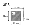
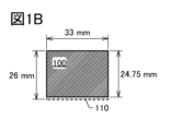
- 1A to 1F are diagrams for explaining the size of a display section and an exposure area.
- 2A and 2B are diagrams for explaining an example of the number of chips obtained from a Si wafer.
- 3A and 3B are diagrams for explaining an example of the number of chips obtained from a Si wafer.
- 4A and 4B are diagrams for explaining an example of the number of chips obtained from a Si wafer.
- 5A and 5B are diagrams illustrating a configuration example of a semiconductor device.
- 6A and 6B are diagrams illustrating an example of the configuration of an electronic device.
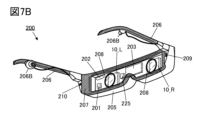
- 7A and 7B are diagrams illustrating an example of the configuration of an electronic device.
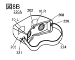
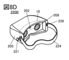
- 8A to 8D are diagrams illustrating examples of the configuration of an electronic device.
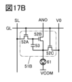
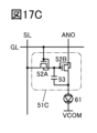
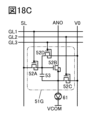
- FIGS. 18A to 18D are diagrams illustrating examples of the configuration of a pixel circuit.
- FIG. 19 is a timing chart illustrating a method of driving the display device.
- Fig. 20A is a block diagram illustrating an example of the configuration of a pixel
- Fig. 20B is a diagram illustrating an example of the configuration of a pixel circuit.
- 21A and 21B are diagrams illustrating a configuration example of a display device.
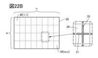
- 22A to 22D are diagrams illustrating a configuration example of a display device.
- 23A to 23C are diagrams illustrating a configuration example of a display device.
- FIG. 24 is a block diagram illustrating an example of the configuration of a display device.
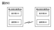
- 25A to 25C are diagrams showing configuration examples of a display device and a display system.
- film and “layer” can be interchanged depending on the circumstances.
- conductive layer can be changed to the term “conductive film.”
- insulating film can be changed to the term “insulating layer.”
- source and drain may be interchangeable when transistors of different polarity are used, or when the direction of current changes during circuit operation. For this reason, in this specification, the terms “source” and “drain” can be used interchangeably.
- electrically connected includes cases where a connection is made via "something that has some kind of electrical action.”
- something that has some kind of electrical action is not particularly limited as long as it allows for the transmission and reception of electrical signals between the connected objects.
- something that has some kind of electrical action includes electrodes or wiring, as well as switching elements such as transistors, resistive elements, coils, capacitive elements, and other elements with various functions.
- the normally-on characteristic refers to a state in which a channel exists and current flows through the transistor even when no voltage is applied to the gate.
- the normally-off characteristic refers to a state in which no current flows through the transistor when no potential is applied to the gate or when a ground potential is applied to the gate.
- a tapered shape refers to a shape in which at least a portion of the side of the structure is inclined with respect to the substrate surface or the surface to be formed.
- the side of the structure, the substrate surface, and the surface to be formed do not necessarily need to be completely flat, and may be approximately planar with a slight curvature, or approximately planar with fine irregularities.
- SIMS secondary ion mass spectrometry
- XPS X-ray photoelectron spectroscopy
- SIMS is suitable when the content of the target element is high (e.g., 0.5 atomic% or more, or 1 atomic% or more).
- SIMS is suitable when the content of the target element is low (e.g., 0.5 atomic% or less, or 1 atomic% or less).
- a device fabricated using a metal mask or FMM fine metal mask, high-definition metal mask
- a device with an MM (metal mask) structure a device with an MML (metal maskless) structure.
- SBS Side By Side
- the SBS structure allows the materials and configuration to be optimized for each light-emitting device, which increases the freedom of material and configuration selection and makes it easier to improve brightness and reliability.
- holes or electrons may be referred to as "carriers".
- the hole injection layer or electron injection layer may be referred to as the "carrier injection layer”
- the hole transport layer or electron transport layer may be referred to as the “carrier transport layer”
- the hole block layer or electron block layer may be referred to as the "carrier block layer”.
- the above-mentioned carrier injection layer, carrier transport layer, and carrier block layer may not be clearly distinguishable.
- one layer may have two or three functions among the carrier injection layer, carrier transport layer, and carrier block layer.
- a light-emitting device has an EL layer between a pair of electrodes.
- the EL layer has at least a light-emitting layer.
- the layers (also called functional layers) that the EL layer has include a light-emitting layer, a carrier injection layer (hole injection layer and electron injection layer), a carrier transport layer (hole transport layer and electron transport layer), and a carrier block layer (hole block layer and electron block layer).
- a light-receiving device also called a light-receiving element
- one of the pair of electrodes may be referred to as a pixel electrode, and the other as a common electrode.
- the display unit can support various screen ratios, for example, 1:1 (square), 4:3, 16:9, and 16:10.
- the external shape of the display unit can have various configurations, such as a square, rectangle, or circle.
- the size of the semiconductor device 100 can be determined based on the exposure area 110 of the exposure device, thereby making it possible to manufacture the semiconductor device at an optimal manufacturing cost.
- the exposure device may be a stepper or a scanner.
- examples of the wavelength of the light source that can be used in the exposure device include 13 nm (EUV (Extreme Ultra Violet)), 157 nm (F 2 ), 193 nm (ArF), 248 nm (KrF), 308 nm (XeCl), 365 nm (i-line), and 436 nm (g-line).
- the explanation will be given using the exposure area 120 of the exposure device, the semiconductor device 100 which is a semiconductor device provided inside the exposure area 120, the sealing area 122 which is a region provided between the semiconductor device 100 and the exposure area 120, the terminal area 126 which is a region provided on one side of the exposure area 120, and the chip exterior area 124 which is a region that is not used when the chip is taken out from the Si wafer.
- the semiconductor device 100 corresponds to the display unit
- the exposure area 120 corresponds to the outer shape of the chip.
- a marker area or the like may be provided in the sealing area 122.
- Figures 4A and 4B each show an example in which a sealing region 122 with a width of 1 mm is provided inside an exposure region 120 of 23 mm x 25 mm. Note that the configuration of the sealing region 122 is the same as that shown in Figures 2A and 2B. In this case, the diagonal size of the semiconductor device 100 is approximately 1.2 inches, and the aspect ratio is 1:1 (hereinafter referred to as 1.2 inches (1:1)).
- 44 1.2 inch (1:1) chips can be extracted from a ⁇ 8 inch Si wafer
- 104 1.2 inch (1:1) chips can be extracted from a ⁇ 12 inch Si wafer.
- the area of the ⁇ 8 inch Si wafer is taken as 100%
- the area outside the chip 124 shown in FIG. 4A is 19%.
- the area outside the chip 124 shown in FIG. 4B is 15%.
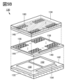
- Fig. 5A and Fig. 5B are perspective views illustrating a semiconductor device of one embodiment of the present invention.
- a display unit 136 capable of displaying at a resolution of so-called super high vision (also called “8K resolution”, “8K4K”, or “8K”).
- super high vision also called "8K resolution”, “8K4K”, or “8K”
- the display unit 136 can support a variety of screen ratios, such as 1:1 (square), 4:3, 16:9, and 16:10.
- FIG. 5B shows a perspective view that illustrates the configuration of each layer provided between substrate 132 and substrate 134.
- a layer 142 is provided over the substrate 132.
- the layer 142 includes a driver circuit 150, a functional circuit 152, and an input/output circuit 154.
- a transistor having silicon in a channel formation region also referred to as an "Si transistor” or “SiFET” or a transistor having an oxide semiconductor in a channel formation region (also referred to as an "OS transistor” or “OSFET”) can be used.
- Si transistor Si transistor
- OS transistor oxide semiconductor in a channel formation region
- a transistor having polycrystalline silicon in a channel formation region may be provided in layer 142.
- Low temperature polysilicon LTPS: Low Temperature Poly Silicon
- LTPS transistor a transistor having LTPS in a channel formation region is also called an "LTPS transistor.”
- the driver circuit 150 has, for example, a gate driver circuit, a source driver circuit, and the like.
- the driver circuit 150 may have an arithmetic circuit, a memory circuit, a power supply circuit, and the like.
- the gate driver circuit, the source driver circuit, and other circuits can be arranged overlapping the display portion 136, the width of the non-display area (also called a frame) present on the periphery of the display portion 136 of the semiconductor device 130 can be made extremely narrow compared to the case where these circuits and the display portion 136 are arranged side by side, and the semiconductor device 130 can be made smaller.
- the functional circuit 152 has, for example, the function of an application processor for controlling each circuit in the semiconductor device 130 and generating signals for controlling each circuit.
- the functional circuit 152 may also have a circuit for correcting image data such as an accelerator such as a CPU or GPU.
- the functional circuit 152 may also have an LVDS (Low Voltage Differential Signaling) circuit that functions as an interface for receiving image data from outside the semiconductor device 130, a MIPI (Mobile Industry Processor Interface) circuit, and a D/A (Digital to Analog) conversion circuit.
- the functional circuit 152 may also have a circuit for compressing and expanding image data, a power supply circuit, etc.
- a layer 144 is provided over the layer 142.
- the layer 144 has a pixel circuit group 158 including a plurality of pixel circuits 156.
- the layer 144 may include an OS transistor.
- the pixel circuit 156 may include an OS transistor. Note that the layer 144 can be stacked over the layer 142.
- the pixel circuit 156 may be configured with multiple types of transistors using different semiconductor materials.
- the transistors may be provided in different layers for each type of transistor.
- the Si transistors and the OS transistors may be provided in a stacked state. By providing the transistors in a stacked state, the area occupied by the pixel circuit 156 is reduced. Therefore, the resolution of the semiconductor device 130 can be improved.
- LTPO a configuration in which LTPS transistors and OS transistors are combined may be referred to as LTPO.
- Layer 146 is provided on layer 144.
- Substrate 134 is provided on layer 146.
- Substrate 134 is preferably a light-transmitting substrate or a layer made of a light-transmitting material.
- Layer 146 is provided with a plurality of light-emitting devices 160.
- layer 146 can be configured to be stacked on layer 144.
- organic electroluminescence elements also called organic EL elements
- light-emitting devices 160 are not limited to this, and for example, inorganic EL elements made of inorganic materials can be used.
- “organic EL elements” and “inorganic EL elements” may be collectively referred to as "EL elements”.
- Light-emitting devices 160 may have inorganic compounds such as quantum dots.
- quantum dots can be used in the light-emitting layer to function as a light-emitting material.
- the semiconductor device 130 of one embodiment of the present invention can have a stacked structure of the light-emitting device 160, the pixel circuit 156, the driver circuit 150, and the functional circuit 152, and therefore the aperture ratio of the pixel (effective display area ratio) can be extremely high.
- the aperture ratio of the pixel can be 40% or more and less than 100%, preferably 50% or more and 95% or less, and more preferably 60% or more and 95% or less.
- the pixel circuits 156 can be arranged at an extremely high density, and the resolution of the pixel can be extremely high.
- pixels with a resolution of 1000 ppi or more, 2000 ppi or more, preferably 3000 ppi or more, more preferably 5000 ppi or more, and even more preferably 6000 ppi or more, and 10000 ppi or less, 20000 ppi or less, or 30000 ppi or less.
- a resolution of 1000 ppi or more and 10000 ppi or less is preferable.
- Such a semiconductor device 130 has extremely high resolution, it can be suitably used in VR devices such as head-mounted displays, or in glasses-type AR devices. For example, even in a configuration in which the display unit of the semiconductor device 130 is viewed through an optical component such as a lens, the semiconductor device 130 has an extremely high-resolution display unit, so that even if the display unit is enlarged with a lens, the pixels are not visible, and a highly immersive display can be achieved.
- This embodiment can be implemented by combining at least a portion of it with other embodiments described in this specification.
- Embodiment 2 In this embodiment, an electronic device and a display device according to one embodiment of the present invention will be described.
- the embodiment of the present invention can be suitably used for, for example, a wearable electronic device for VR or AR.
- FIG. 6A shows a perspective view of a glasses-type electronic device 200 as an example of a wearable electronic device.
- a pair of display devices 10 (a display device 10_L and a display device 10_R), a motion detection unit 201, a gaze detection unit 202, a calculation unit 203, and a communication unit 204 are provided in a housing 205.
- FIG. 6B is a block diagram of electronic device 200 of FIG. 6A.
- electronic device 200 has display device 10_L, display device 10_R, motion detection unit 201, gaze detection unit 202, calculation unit 203, and communication unit 204, and transmits and receives various signals between them via bus wiring BW.
- Display device 10_L and display device 10_R each have multiple pixels 230, drive circuit 30, and function circuit 40.
- One pixel 230 includes one light-emitting element 61 and one pixel circuit 51.
- display device 10_L and display device 10_R each include multiple light-emitting elements 61 and multiple pixel circuits 51.
- the motion detection unit 201 has a function of detecting the movement of the housing 205, that is, the movement of the head of the user wearing the electronic device 200.
- the motion detection unit 201 may use, for example, a motion sensor using MEMS technology.
- a motion sensor using MEMS technology.
- a three-axis motion sensor or a six-axis motion sensor may be used.
- Information regarding the movement of the housing 205 detected by the motion detection unit 201 may be referred to as first information or motion information.
- the gaze detection unit 202 has a function of acquiring information about the user's gaze. Specifically, it has a function of detecting the user's gaze.
- the user's gaze may be acquired by an eye tracking method such as the Pupil Center Corneal Reflection method or the Bright/Dark Pupil Effect method. Alternatively, it may be acquired by an eye tracking method using a laser or ultrasonic waves. Alternatively, the user's gaze may be detected by using an imaging element such as an image sensor. Examples of image sensors include a CMOS (Complementary Metal Oxide Semiconductor) image sensor and a CCD (Charge Coupled Device) image sensor.
- CMOS Complementary Metal Oxide Semiconductor
- CCD Charge Coupled Device
- the calculation unit 203 has a function of performing drawing processing (calculation processing of image data) according to the movement of the housing 205.
- the drawing processing according to the movement of the housing 205 in the calculation unit 203 is performed using the first information and image data input from the outside via the communication unit 204.
- 360-degree omnidirectional image data can be used as the image data.
- the 360-degree omnidirectional image data may be, for example, image data captured by an omnidirectional camera (omnidirectional camera, 360° camera), or may be image data generated by computer graphics or the like.
- the calculation unit 203 has a function of converting the 360-degree omnidirectional image data according to the first information into image data that can be displayed on the display device 10_L and the display device 10_R.
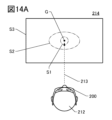
- the calculation unit 203 also has a function of using the second information to determine the size and shape of multiple areas to be set on the display unit of each of the display devices 10_L and 10_R. Specifically, the calculation unit 203 calculates a gaze point on the display unit according to the second information, and sets a first area S1 to a third area S3, etc. (described later) on the display unit based on the gaze point.
- calculation unit 203 in addition to a central processing unit (CPU: Central Processing Unit), other microprocessors such as a DSP (Digital Signal Processor) and a GPU (Graphics Processing Unit) can be used alone or in combination. These microprocessors may also be realized by a PLD (Programmable Logic Device) such as an FPGA (Field Programmable Gate Array) or an FPAA (Field Programmable Analog Array).
- CPU Central Processing Unit
- DSP Digital Signal Processor
- GPU Graphics Processing Unit
- PLD Programmable Logic Device
- FPGA Field Programmable Gate Array
- FPAA Field Programmable Analog Array
- the calculation unit 203 performs various data processing and program control by interpreting and executing commands from various programs using the processor.
- the programs that can be executed by the processor may be stored in a memory area of the processor, or may be stored in a separately provided storage unit.
- the storage unit for example, a storage device using non-volatile storage elements such as flash memory, MRAM (Magnetoresistive Random Access Memory), PRAM (Phase change RAM), ReRAM (Resistive RAM), and FeRAM (Ferroelectric RAM), or a storage device using volatile storage elements such as DRAM (Dynamic RAM) and SRAM (Static RAM) may be used.
- the communication unit 204 has the function of communicating with external devices wirelessly or via wires to obtain various data such as image data.
- the communication unit 204 may be provided with, for example, a high-frequency circuit (RF circuit) and transmit and receive RF signals.
- the high-frequency circuit is a circuit that converts between electromagnetic signals and electrical signals in a frequency band determined by the legislation of each country, and uses the electromagnetic signals to communicate wirelessly with other communication devices.
- communication standards such as LTE (Long Term Evolution), GSM (Global System for Mobile Communication: registered trademark), EDGE (Enhanced Data Rates for GSM Evolution), CDMA2000 (Code Division Multiple Access 2000), WCDMA (Wideband Code Division Multiple Access: registered trademark), or IEEE communication standard specifications such as Wi-Fi (registered trademark), Bluetooth (registered trademark), and ZigBee (registered trademark) can be used as communication protocols or communication technologies.
- LTE Long Term Evolution
- GSM Global System for Mobile Communication: registered trademark
- EDGE Enhanced Data Rates for GSM Evolution
- CDMA2000 Code Division Multiple Access 2000
- WCDMA Wideband Code Division Multiple Access: registered trademark
- IEEE communication standard specifications such as Wi-Fi (registered trademark), Bluetooth (registered trademark), and ZigBee (registered trademark)
- 3G third generation mobile communication system
- 4G fourth generation mobile communication system
- 5G fifth generation mobile communication system defined by the International Telecommunications Union (ITU)
- ITU International Telecommunications Union
- the communication unit 204 may also have external ports such as a terminal for connecting to a LAN (Local Area Network), a terminal for receiving digital broadcasts, and a terminal for connecting an AC adapter.
- a terminal for connecting to a LAN Local Area Network
- a terminal for receiving digital broadcasts and a terminal for connecting an AC adapter.
- the display device 10_L and the display device 10_R each have a plurality of light-emitting elements 61, a plurality of pixel circuits 51, a drive circuit 30, and a function circuit 40.
- the pixel circuit 51 has a function of controlling the light emission of the light-emitting elements 61.
- the drive circuit 30 has a function of controlling the pixel circuit 51.
- the information on the multiple regions in the display unit of the display device 10 determined by the calculation unit 203 is used for driving the display unit 10 to provide different resolutions for each region.
- the functional circuit 40 has a function of controlling the drive circuit 30 to provide a high-resolution display in regions close to the gaze point, and to provide a low-resolution display in regions far from the gaze point.
- the function of outputting a control signal for the drive circuit 30 can be separated from the calculation unit 203 and performed by the functional circuit 40. Therefore, the load is not concentrated on one calculation unit, and the load on the calculation unit can be suppressed. Therefore, it is possible to reduce the power consumption overall.
- the electronic device 200 may also be provided with a sensor 225.
- the sensor 225 may have a function of acquiring information on one or more of the user's vision, hearing, touch, taste, and smell. More specifically, the sensor 225 may have a function of detecting or measuring information on one or more of force, displacement, position, speed, acceleration, angular velocity, rotation speed, distance, light, magnetism, temperature, sound, time, electric field, current, voltage, power, radiation, humidity, gradient, vibration, odor, and infrared light.
- the electronic device 200 may be provided with one or more sensors 225.
- the electronic device may further include an earphone 206A.
- the earphone 206A includes a communication unit (not shown) and has a wireless communication function.
- the earphone 206A can output audio data using the wireless communication function.
- the earphone 206A may also include a vibration mechanism in order to function as a bone conduction earphone.
- the user can see one display device per eye. This makes it possible to display high-resolution images even when performing 3D display using parallax.
- the display device 10 is curved in an arc shape roughly centered on the user's eye. This makes it possible for the user to see more natural images because the distance from the user's eye to the display surface of the display device 10 is constant.
- the user's eyes can be configured to be positioned in the normal direction to the display surface of the display device 10, so that the effect can be essentially ignored, especially in the horizontal direction, making it possible to display more realistic images.
- the display device 10 can display two images, one for the right eye and one for the left eye, side by side in two areas, one on the left and one on the right. This makes it possible to display a stereoscopic image using binocular parallax.
- FIG. 9A is a perspective view of a display device 10A that can be used with the display devices 10_L and 10_R shown in FIGS. 6A and 6B.
- the transistor 21 can be, for example, a transistor having single crystal silicon in the channel formation region (also called a "c-Si transistor"). This is preferable because it allows the on-current of the transistor to be increased and allows the circuit in the layer 20 to be driven at high speed.
- a Si transistor can be formed by microfabrication so that the channel length is 3 nm or more and 10 nm or less, it is possible to form the display device 10A in which a CPU, an accelerator such as a GPU, an application processor, etc. are integrated with the display unit.
- transistors using polycrystalline silicon such as low-temperature polysilicon may be applied to layer 20.
- OS transistors may be provided in layer 20 as necessary.
- a thin-film transistor using a thin film as a semiconductor in which a channel is formed such as a Poly-Si transistor, an LTPS transistor, or an OS transistor
- an insulating substrate that is less expensive than a semiconductor substrate can be used as the substrate.
- a bendable display device can be obtained.
- the function circuit 40 the pixel circuit group 55 including a plurality of pixel circuits 51, etc., please refer to the above description.
- the diagonal size of the display unit 13 can be 0.1 inches or more and 5.0 inches or less, preferably 0.5 inches or more and 2.0 inches or less, and more preferably 1 inch or more and 1.7 inches or less.
- the diagonal size of the display unit 13 can be 1.5 inches or close to 1.5 inches.
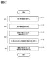
- the gaze point G When the gaze 213 of the user 212 moves, the gaze point G also moves. Therefore, the first area S1 and the second area S2 also move. For example, when the amount of change in the gaze 213 exceeds a certain amount, it is determined that the gaze 213 has moved. In other words, when the amount of change in the gaze point G exceeds a certain amount, it is determined that the gaze point G has moved. Also, when the amount of change in the gaze 213 falls below a certain amount, it is determined that the movement of the gaze 213 has stopped, and the first area S1 to the third area S3 are determined. In other words, when the amount of change in the gaze point G falls below a certain amount, it is determined that the movement of the gaze point G has stopped, and the first area S1 to the third area S3 are determined.
- the pixel circuit 51A shown in FIG. 17A includes a transistor 52A, a transistor 52B, and a capacitor 53.
- FIG. 17A also shows a light-emitting element 61 connected to the pixel circuit 51A.
- the pixel circuit 51A is electrically connected to wiring SL, wiring GL, wiring ANO, and wiring VCOM.
- the pixel circuit 51A has a configuration in which the transistor 52C is removed from the pixel circuit 51 shown in FIG. 16A, and wiring GL1 and wiring GL2 are replaced with wiring GL.
- the pixel circuit 51I shown in FIG. 20B has a transistor 52w, a transistor 52A, a transistor 52B, a transistor 52C, a capacitance 53s, and a capacitance 53w.
- the transistor 52A and the capacitance 53w form a memory circuit MEM.
- FIG. 20B also shows a light-emitting element 61 connected to the pixel circuit 51I.
- node NM the node to which the other electrode of capacitance 53w, one of the source or drain of transistor 52A, the gate of transistor 52B, and one electrode of capacitance 53s are connected.
- node NA the node to which the other electrode of capacitance 53s, one of the source or drain of transistor 52B, one of the source or drain of transistor 52C, and one electrode of light-emitting element 61 are connected.
- the gate of transistor 52w is electrically connected to wiring GL1.
- the gate of transistor 52C is electrically connected to wiring GL1.
- the gate of transistor 52A is electrically connected to wiring GL2.
- the other of the source and drain of transistor 52w is electrically connected to wiring SL1.
- the other of the source and drain of transistor 52C is electrically connected to wiring V0.
- the other of the source and drain of transistor 52A is electrically connected to wiring SL2.
- wirings SL1 and SL2 may be collectively referred to as wirings SL. Therefore, the number of wirings SL is not limited to one, and may be multiple.
- the display device 10B has a pixel circuit group 55 including a plurality of pixel circuits 51 (not shown) and a drive circuit 30 stacked on top of each other.
- the pixel circuit group 55 is divided into a plurality of sections 59
- the drive circuit 30 is divided into a plurality of sections 39.
- Each of the plurality of sections 39 has a source driver circuit 31 and a gate driver circuit 33.
- the input/output circuit 252 outputs information photoelectrically converted by the light receiving element to the function circuit 40.
- Lowering the drive frequency can reduce the power consumption of the display device.
- lowering the drive frequency also reduces the display quality.
- the display quality when displaying moving images is reduced.
- by making the second drive frequency lower than the first drive frequency it is possible to reduce the power consumption in areas where the user's visibility is low, while suppressing the substantial degradation of the display quality.
- the first drive frequency may be 30 Hz or more and 500 Hz or less, preferably 60 Hz or more and 500 Hz or less.
- the second drive frequency is preferably equal to or less than the first drive frequency, more preferably equal to or less than 1/2 the first drive frequency, and even more preferably equal to or less than 1/5 the first drive frequency.
- the area farther from the first area 29A may be set as the third area 29C (see FIG. 23C), and the drive frequency (also referred to as the "third drive frequency") of the sub-display units 19 included in the third area 29C may be set lower than that of the second area 29B.
- the third drive frequency is preferably equal to or lower than the second drive frequency, more preferably equal to or lower than 1/2 the second drive frequency, and even more preferably equal to or lower than 1/5 the second drive frequency.
- the image data in areas other than the first area 29A may be rewritten at the same drive frequency as the first area 29A, and if it is determined that the amount of change is within the certain amount, the drive frequency in areas other than the first area 29A may be reduced. Furthermore, if it is determined that the amount of change in the gaze point G is small, the drive frequency in areas other than the first area 29A may be further reduced.
- the second drive frequency and the third drive frequency must both be an integer division of the first drive frequency.
- image data temporary storage unit 263 and the frame memory 253 may be flash memory, MRAM, PRAM, ReRAM, FeRAM, DRAM, or SRAM. Further, the image data temporary storage unit 263 and the frame memory 253 may be DOSRAM (registered trademark), NOSRAM (registered trademark), or the like.
- each of the multiple sections 39 has a source driver circuit 31, a gate driver circuit 33, a timing generation circuit 251, and an input/output circuit 252.
- the timing generation circuit 251 in section 39[1,1] is shown as timing generation circuit 251[1,1].
- the input/output circuit 252 in section 39[1,1] is shown as input/output circuit 252[1,1].
- the image information input unit 261 receives image data to be displayed on the display unit 13 and operating parameters of the display device 10B from the outside.
- the clock signal input unit 262 receives a clock signal from the outside.
- the clock signal is also supplied to the internal clock signal generation unit 265 via the clock signal input unit 262.
- the image data input via the image information input unit 261 is supplied to the image data temporary storage unit 263.
- the operation parameters input via the image information input unit 261 are supplied to the operation parameter setting unit 264.
- the image data temporary storage unit 263 holds the supplied image data and supplies the image data to the image processing unit 266 in synchronization with an internal clock signal. Therefore, the image data temporary storage unit 263 is also a type of frame memory. By providing the image data temporary storage unit 263, it is possible to eliminate the discrepancy between the timing at which image data is supplied from the outside and the timing at which the image data is processed inside the display device 10B.
- the image processing unit 266 has a function of performing arithmetic processing of the image data stored in the image data temporary storage unit 263. For example, it has a function of performing contrast adjustment, brightness adjustment, and gamma correction of the image data.
- the image processing unit 266 also has a function of dividing the image data stored in the image data temporary storage unit 263 for each sub-display unit 19.
- the image processing unit 266 also has the function of reading out image data stored in each of the multiple frame memories 253, performing arithmetic processing on the image data, and writing the processed image data back to the frame memory 253. For example, when a still image is displayed on the display unit 13, it is possible to adjust brightness, contrast, and the like by performing arithmetic processing on the image data stored in some or all of the multiple frame memories 253.
- the memory controller 267 has a function of controlling the operation of each of the multiple frame memories 253.
- the image data divided for each sub-display unit 19 by the image processing unit 266 is stored in each of the multiple frame memories 253.
- the multiple frame memories 253 have a function of supplying image data to the sections 39 in response to a read request signal (read) from the corresponding section 39.
- the storage device 41 may be used instead of the frame memory 253.
- the image data divided for each sub-display unit 19 may be stored in the storage device 41.
- the frame memory 253 may also be provided in a device other than the functional circuit 40.
- the frame memory 253 may also be provided in a semiconductor device other than the display device 10B.
- the image displayed in the first area 29A may be subjected to the above-mentioned upconversion process.
- the display quality can be improved.
- the image displayed in an area other than the first area 29A may be subjected to the above-mentioned upconversion process.
- the actual decrease in display quality when the drive frequency in an area other than the first area 29A is reduced can be reduced.
- the source driver circuit writes image data to all pixels in one row simultaneously while the gate driver circuit selects the pixels in one row.
- the source driver circuit needs to write image data to 4000 pixels while the gate driver circuit selects the pixels in one row.
- the frame frequency is 120 Hz
- the time for one frame is approximately 8.3 msec. Therefore, the gate driver circuit needs to select 2000 rows of pixels in approximately 8.3 msec, and the time for selecting one row of pixels, that is, the time for writing image data per pixel, is approximately 4.17 ⁇ sec.
- the higher the resolution of the display section and the higher the frame frequency the more difficult it becomes to ensure sufficient time for rewriting image data.
- the display unit 13 is divided into four in the row direction, so the length of the wiring SL that electrically connects the source driver circuit and the pixel circuit is reduced to one-quarter. As a result, the resistance value and parasitic capacitance of the wiring SL are each reduced to one-quarter, and the time required to write (rewrite) image data can be shortened.
- the display unit 13 is divided into eight in the column direction, so the length of the wiring GL that electrically connects the gate driver circuit and the pixel circuit is reduced to one-eighth.
- the resistance value and parasitic capacitance of the wiring GL are each reduced to one-eighth, improving signal degradation and delay and making it easier to ensure the time required for rewriting image data.
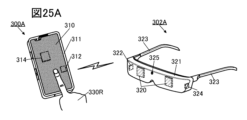
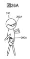
- the user can use intuitive gesture operations to manipulate images (also called data objects) displayed on the display unit 320 of the second display device 302A as if they were real objects.
- images also called data objects
- the user may register specific gesture operations in advance on the second display device 302A and link them to specific processes.
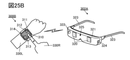
- FIG. 25B An example of a configuration different from that shown in FIG. 25A will be explained using FIG. 25B.
- the first display device 300A shown in FIG. 25A has a function as a so-called mobile information terminal (typically a smartphone, etc.), and the first display device 300B shown in FIG. 25B has a function as a so-called wristwatch-type mobile information terminal.
- the first display device 300A and the first display device 300B have at least one or both of a calling function and a time display function.
- the second display device 302A has a function to display content of augmented reality (AR), virtual reality (VR), substitutional reality (SR), or mixed reality (MR).
- AR augmented reality
- VR virtual reality
- SR substitutional reality
- MR mixed reality
- the first display device 300A has a period during which the display unit does not display anything, and during this period, it functions as an input/output unit (e.g., a controller) for the second display device 302A.
- an input/output unit e.g., a controller
- the display system that is one embodiment of the present invention can reduce power consumption.
- the display unit 310 and the display unit 320 each have a display function.
- a liquid crystal display device a light-emitting device including an organic EL
- a light-emitting device including a light-emitting diode such as a micro LED
- productivity and light-emitting efficiency are taken into consideration, it is preferable to use a light-emitting device including an organic EL as the display unit 310 and the display unit 320.
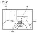
- FIG. 26B shows an example of image 340 shown in FIG. 26A and displayed in the field of view of user 330 in a room.
- image information 341 is shown superimposed on an image of the actual interior scenery, such as the floor, walls, and doors.
- image information 341 is part of the image displayed on the display unit of first display device 300A.
- user 330 can also operate first display device 300A (e.g., a smartphone) paired with second display device 302A.
- second display device 302A recognizes this movement as a gesture operation and makes the shape of image information 341 changeable.
- image information 341 is deformed so as to shrink, as shown in FIG. 26D.
- image information 341 can be enlarged.
- image information 341 can also be moved or rotated following the movement of left hand 330L and right hand 330R. Image information 341 may also be scrolled.
- step S01 the operation starts.
- the first display device 300A is in an activated state (a state in which operation is possible), and the second display device 302A is in a powered-on state.
- the pixel density of the display unit differs between the first display device 300A and the second display device 302A, it is preferable to display the second image on the second display device 302A after performing image processing such as up-conversion or down-conversion on the first image so that the image has an optimal size when displayed on the display unit 320 of the second display device 302A, rather than displaying the first image as is.
- step S05 information is transmitted from the second display device 302A to the first display device 300A.
- the information includes a code indicating that the display of the first image has been completed.
- the second display device 302A detects a gesture movement by the user using a detection unit included in the second display device 302A, and obtains gesture information corresponding to the gesture movement. If the second display device 302A has multiple detection units, the gesture movement is detected by all or two or more of the multiple detection units. This makes it possible to detect three-dimensional position information of multiple objects with higher accuracy, thereby enabling input by complex gesture operations.
- step S08 the second display device 302A executes various processes based on the gesture information. For example, image processing can be performed on the image information displayed on the display unit 320 of the second display device 302A, and the image information after image processing can be displayed on the display unit 320.
- Step S09 corresponds to, for example, removing the second display device 302A, turning off the power of the first display device 300A or the second display device 302A, or canceling the pairing between the first display device 300A and the second display device 302A.
- an insulator 420 and an insulator 422 are stacked in this order from the substrate 410 side.
- the insulator 598 is an insulator having barrier properties against one or more selected from hydrogen, oxygen, and water, similar to the insulator 592.
- the insulator 599 is an insulator having a relatively low dielectric constant, similar to the insulator 594, in order to reduce the parasitic capacitance that occurs between wirings.
- the insulator 599 functions as an interlayer insulating film and a planarizing film.
- the display device 600A employs an SBS structure.
- the SBS structure allows the materials and configuration to be optimized for each light-emitting device, allowing greater freedom in the selection of materials and configurations, making it easier to improve brightness and reliability.
- layer 613a is formed so as to cover the upper and side surfaces of conductor 611a.
- layer 613b is formed so as to cover the upper and side surfaces of conductor 611b.
- layer 613c is formed so as to cover the upper and side surfaces of conductor 611c. Therefore, the entire area in which conductors 611a, 611b, and 611c are provided can be used as the light-emitting areas of light-emitting device 650R, light-emitting device 650G, and light-emitting device 650B, thereby increasing the aperture ratio of the pixel.
- the insulator 627 can be formed using a wet film formation method such as spin coating, dipping, spray coating, inkjet, dispensing, screen printing, offset printing, doctor knife method, slit coating, roll coating, curtain coating, or knife coating.
- a wet film formation method such as spin coating, dipping, spray coating, inkjet, dispensing, screen printing, offset printing, doctor knife method, slit coating, roll coating, curtain coating, or knife coating.
- the insulator 627 is formed at a temperature lower than the heat resistance temperature of the EL layer.
- the substrate temperature when forming the insulator 627 is typically 200°C or less, preferably 180°C or less, more preferably 160°C or less, more preferably 150°C or less, and more preferably 140°C or less.
- the upper surface of the insulator 627 preferably has a convex curved shape.
- the convex curved shape of the upper surface of the insulator 627 is preferably a shape that bulges gently toward the center.
- it is preferable that the convex curved portion at the center of the upper surface of the insulator 627 is smoothly connected to the tapered portion at the end of the side surface.
- one end of the insulator 627 overlaps with the conductor 611a that functions as a pixel electrode, and the other end of the insulator 627 overlaps with the conductor 611b that functions as a pixel electrode.
- the end of the insulator 627 can be formed on a flat or approximately flat region of the layer 613a (layer 613b). Therefore, it becomes relatively easy to process the tapered shape of the insulator 627 as described above.
- the display device of this embodiment has an area where the distance between two adjacent island-shaped EL layers is 1 ⁇ m or less, preferably an area where the distance is 0.5 ⁇ m (500 nm) or less, and more preferably an area where the distance is 100 nm or less. In this way, by narrowing the distance between each light-emitting device, a display device with high definition and large aperture ratio can be provided.
- a protective layer 631 is provided on the light-emitting device 650.
- the protective layer 631 is a film that functions as a passivation film that protects the light-emitting device 650.
- impurities such as water and oxygen are prevented from entering the light-emitting device, and the reliability of the light-emitting device 650 can be improved.
- aluminum oxide, silicon nitride, or silicon oxynitride can be used for the protective layer 631.
- Display device 600A is a top emission type. Light emitted by the light emitting device is emitted towards substrate 610. For this reason, it is preferable to use a material that is highly transparent to visible light for substrate 610. For example, a substrate that is highly transparent to visible light may be selected for substrate 610 from among the substrates that can be used for substrate 410.
- the pixel electrode contains a material that reflects visible light
- the opposing electrode (common electrode 615) contains a material that transmits visible light.
- the display device of one embodiment of the present invention may be a bottom emission type in which light emitted from a light-emitting device is emitted toward the substrate 410, rather than a top emission type.
- a substrate that has high transparency to visible light may be selected as the substrate 410.
- the element layer 630 of the display device 600A in FIG. 28 includes a transistor MTCK, but this is not limited thereto.
- the structure of the transistor included in the display device of one embodiment of the present invention is not particularly limited.
- One or more types of transistors can be used in the display device of one embodiment of the present invention.
- the transistor MTCK shown in FIG. 31, the transistor MTCK2 shown in FIG. 32, and the transistor 800 shown in FIG. 33 can be used.
- the display device of one embodiment of the present invention can include one or both of an OS transistor and a Si transistor.
- FIG. 29 shows a cross-sectional view of the display device 600B.
- the display device 600B can be a flexible display device (also called a flexible display) by using flexible substrates for the substrate 501 and the substrate 610.
- the substrate 501 is attached to the insulating layer 505 by an adhesive layer 503.
- the substrate 610 is attached to the protective layer 631 by an adhesive layer 607. An example of a method for manufacturing a flexible device will be described later in this embodiment.
- the element layer 660 of the display device 600B differs from the element layer 660 of the display device 600A mainly in that the same configuration is applied to the layers 613a, 613b, and 613c, and further in that the colored layers 628R, 628G, and 628B are provided.
- the light emitted by light-emitting device 650R is extracted as red light to the outside of display device 600B via colored layer 628R.
- the light emitted by light-emitting device 650G is extracted as green light to the outside of display device 600B via colored layer 628G.
- the light emitted by light-emitting device 650B is extracted as blue light to the outside of display device 600B via colored layer 628B.
- tandem structure for a light-emitting device that emits white light.
- An example of the configuration of a light-emitting device with a tandem structure will be described in detail in embodiment 5.
- the light-emitting devices 650R, 650G, and 650B shown in FIG. 29 emit blue light.
- the layers 613a, 613b, and 613c each have one or more light-emitting layers that emit blue light.
- the blue light emitted by the light-emitting device 650B can be extracted.
- a color conversion layer is provided between the light-emitting device 650R and the colored layer 628R and between the light-emitting device 650G and the colored layer 628G, so that the blue light emitted by the light-emitting device 650R or the light-emitting device 650G can be converted into light with a longer wavelength, and red or green light can be extracted.
- the colored layer absorbs light other than the desired color, and the color purity of the light that the subpixel emits can be increased.
- the colored layers are colored layers that selectively transmit light in a specific wavelength range and absorb light in other wavelength ranges.
- a red (R) color filter that transmits light in the red wavelength range
- a green (G) color filter that transmits light in the green wavelength range
- a blue (B) color filter that transmits light in the blue wavelength range
- R red
- G green
- B blue
- metal materials, resin materials, pigments, and dyes can be used.
- the colored layers are formed at the desired positions by a printing method, an inkjet method, an etching method using photolithography, or the like.
- Display device 600B differs from display device 600A in that it does not have element layer 620 but has element layer 635.
- Element layer 635 has the same configuration as element layer 630.
- At least a part of the transistors in the element layer 635 is electrically connected to the conductive layer or the transistors in the element layer 630 via plugs, wiring, etc. Note that a wiring layer 670 may be provided between the element layer 630 and the element layer 635.
- the element layer 635 is provided with one or both of a pixel circuit and a driver circuit of a display device.
- element layer 630 and element layer 635 an example in which two element layers having OS transistors are stacked (element layer 630 and element layer 635) is shown, but the number of stacked element layers is not limited to this, and may be three or more layers.
- the bottom layer is used for the driver circuit (either or both of the gate driver and source driver) of the display device
- the top layer is used for the pixel circuit of the display device
- the layers located between are used for the pixel circuit or driver circuit, respectively.
- Si transistors are typically formed on single crystal Si wafers, making it difficult to make them flexible.
- FIG. 21 when a display device is constructed using only OS transistors without using Si transistors, a flexible configuration can be made using a relatively simple manufacturing process.
- FIG. 30 shows a cross-sectional view of the display device 600C.
- the element layer 660 of the display device 600C has a similar configuration to the element layer 660 of the display device 600B, so a detailed description will be omitted.
- the element layer 630 and the element layer 635 of the display device 600C each have a plurality of transistors MTCK and a plurality of transistors MTCK2.
- the transistor MTCK has an extremely small channel length and can have a large channel width, and can achieve a high on-current.
- the transistor MTCK2 has an extremely small channel width and can have a large channel length, and can achieve a moderate on-current, making design easy.
- the transistor MTCK2 can share part of the manufacturing process with the transistor MTCK, and can be manufactured separately on the same substrate.
- the transistor MTCK2 can be applied as a drive transistor for controlling the current flowing through a light-emitting device, and the transistor MTCK can be applied as a transistor that functions as a switch.
- element layer 630 and element layer 635 are not limited to the above configuration.
- element layer 635 may be provided on element layer 630, that is, a drive circuit for the display device may be provided on a pixel circuit for the display device.
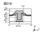
- FIG. 31A to 31C show an example of a semiconductor device (e.g., a pixel circuit or a driving circuit) including a transistor MTCK.
- FIG. 31A shows a schematic plan view of the transistor MTCK.
- FIG. 31B is a schematic cross-sectional view corresponding to the portion of the dashed line A1-A2 shown in FIG. 31A, and is also a schematic cross-sectional view of the transistor MTCK.
- FIG. 31C is a schematic cross-sectional view corresponding to the portion of the dashed line A3-A4 shown in FIG. 31A, and is also a schematic cross-sectional view of the transistor MTCK.
- the direction of the dashed line A1-A2 is the X direction
- the direction of the dashed line A3-A4 is the Y direction.
- the direction perpendicular to the X direction and the Y direction is the Z direction.
- the X direction and the Y direction can be perpendicular to each other.
- the definitions of the X direction, the Y direction, and the Z direction may be the same or different in the following drawings.
- the right side may be called the X direction, the left side the -X direction, the upper side the Y direction, and the lower side the -Y direction.
- the conductor ME1 is provided as a wiring extending in the Y direction, as an example.
- the conductor ME2 is provided as a wiring extending in the X direction, as an example.
- the insulator IS2 functions as an interlayer film that separates the source and drain in the transistor MTCK.
- a material applicable to the insulator IS1 can be used for the insulating film IS2.
- the semiconductor SC1 is a metal oxide that functions as an oxide semiconductor
- the carrier concentration of the metal oxide decreases at the interface and near the interface of the semiconductor SC1 that is in contact with the insulator IS2, and the interface and near the interface of the semiconductor SC1 become i-type or substantially i-type. Therefore, the interface and near the interface of the semiconductor SC1 can function as a channel formation region in the transistor MTCK.
- the semiconductor SC1 is a metal oxide that functions as an oxide semiconductor, it is preferable to form it using the ALD (Atomic Layer Deposition) method. As shown in Figures 31B and 31C, when forming the semiconductor SC1 in a region having a step, the ALD method can be used to form a semiconductor with good coverage.
- ALD Atomic Layer Deposition
- the microwave treatment refers to a treatment using a device having a power source that generates high-density plasma using microwaves, for example.
- In-Ga-Zn oxide for the semiconductor SC1.
- it is more preferable to use a metal oxide having a composition of In:Ga:Zn 1:1:1 [atomic ratio] or a composition close thereto, a composition of 4:2:3 [atomic ratio] or a composition close thereto, or a composition of 3:1:2 [atomic ratio] or a composition close thereto.
- an opening KK1 is formed in the region of the insulator IS2 where the transistor MTCK is provided, and the side surface is approximately perpendicular to the X-Y plane (taper angle is 70° or more and 110° or less). Furthermore, the semiconductor SC1 including the channel formation region of the transistor MTCK is provided so as to be in contact with the conductors ME1 and ME2 through the opening KK1.
- an insulator GI1 is provided on the semiconductor SC1. Specifically, in a plan view, the insulator GI1 is positioned so as to overlap above the channel formation region included in the semiconductor SC1. The insulator GI1 functions as a gate insulating film in the transistor MTCK.
- insulator GI1 it is preferable to use a single layer or a laminate of an insulator containing a so-called high-k material such as aluminum oxide, hafnium oxide, tantalum oxide, zirconium oxide, lead zirconate titanate (PZT), strontium titanate (SrTiO 3 ), or (Ba, Sr)TiO 3 (BST).
- a so-called high-k material such as aluminum oxide, hafnium oxide, tantalum oxide, zirconium oxide, lead zirconate titanate (PZT), strontium titanate (SrTiO 3 ), or (Ba, Sr)TiO 3 (BST).
- an oxide having aluminum and hafnium, an oxynitride having aluminum and hafnium, an oxide having silicon and hafnium, an oxynitride having silicon and hafnium, or a nitride having silicon and hafnium may be used as an insulator with a high relative dielectric constant.
- a material that can be used for the insulator IS1 may be applied.
- silicon oxide, silicon oxynitride, silicon nitride oxide, or silicon nitride may be used.
- the conductor ME3 is provided as wiring extending in the Y direction, as an example.
- the transistor MTCK shown in Figures 31A to 31C the conductor ME1 functioning as either the source or the drain is located below the insulator IS2, which serves as the interlayer film, and the conductor ME2 functioning as the other of the source or the drain is located above the insulator IS2. Therefore, the transistor MTCK is configured such that the channel formation region is provided along the opening of the insulator IS2.
- the source and drain are located at different heights, and the current flowing through the semiconductor layer flows in the height direction.
- the channel length direction can be said to have a height (vertical) component, so the transistor MTCK can also be called a VFET (Vertical Field Effect Transistor), vertical transistor, vertical channel transistor, vertical channel transistor, etc.
- VFET Vertical Field Effect Transistor
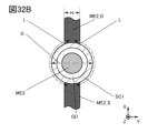
- Fig. 32A shows a cross-sectional view in the XZ plane of a transistor MTCK2 having a different configuration from that in Fig. 31B, and Fig. 32B shows a cross-sectional view in the XY plane.
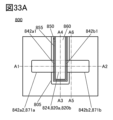
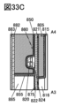
- the channel formation region preferably has a reduced carrier concentration and is i-type or substantially i-type, whereas the source and drain regions preferably have high carrier concentrations and are n-type. That is, it is preferable to reduce oxygen vacancies and VOH in the channel formation region of the oxide semiconductor. It is also preferable to prevent an excessive amount of oxygen from being supplied to the source and drain regions and to prevent the amount of VOH in the source and drain regions from being excessively reduced. It is also preferable to have a structure in which the conductivity of the conductor 860, the conductor 842a, the conductor 842b, and the like is not likely to decrease.
- a conductive material having a function of reducing hydrogen diffusion for the conductor 805a By using a conductive material having a function of reducing hydrogen diffusion for the conductor 805a, it is possible to prevent impurities such as hydrogen contained in the conductor 805b from diffusing to the oxide 820 via the insulator 816, etc.
- a conductive material having a function of suppressing oxygen diffusion for the conductor 805a it is possible to suppress the conductor 805b from being oxidized and its conductivity from decreasing.
- Examples of conductive materials having a function of suppressing oxygen diffusion include titanium, titanium nitride, tantalum, tantalum nitride, ruthenium, and ruthenium oxide.
- the conductor 805a can have a single layer structure or a multilayer structure of the above conductive materials.
- the conductor 805a preferably has titanium nitride.
- a conductive material that is resistant to oxidation or a conductive material that has the function of suppressing the diffusion of oxygen As conductor 842a, conductor 842b, and conductor 860.
- conductive materials include conductive materials that contain nitrogen and conductive materials that contain oxygen. This can suppress a decrease in the conductivity of conductor 842a, conductor 842b, and conductor 860.
- the channel formation region can be electrically surrounded. Since the S-channel structure electrically surrounds the channel formation region, it can be said that it is substantially the same structure as a GAA (Gate All Around) structure or a LGAA (Lateral Gate All Around) structure.
- the transistor 800 By making the transistor 800 have an S-channel structure, a GAA structure, or a LGAA structure, the channel formation region formed at or near the interface between the oxide 820 and the gate insulator can be the entire bulk of the oxide 820. Therefore, it is possible to improve the current density flowing through the transistor, and it is expected that the on-current of the transistor or the field effect mobility of the transistor can be improved.
- the element layer includes elements such as transistors.
- the element layer includes at least one of a display element, wiring electrically connecting to the display element, elements such as transistors used in pixels and circuits, and optical components such as a colored layer and a light-shielding layer.
- each of the two flexible members that sandwich the element layer is referred to as a substrate (or flexible substrate).
- the substrate also includes an extremely thin film with a thickness of 10 nm or more and 300 ⁇ m or less.
- one method is to first laminate a release layer and an insulating layer on a support substrate, form an element layer on the insulating layer, separate the element layer from the support substrate, and transfer the element layer to a substrate.
- a material is selected that will cause separation at the interface between the support substrate and the release layer, the interface between the release layer and the insulating layer, or in the release layer.
- This method is preferable because it is possible to increase the upper limit of the temperature applied when forming the element layer by using a material with high heat resistance for the support substrate and the release layer, and therefore it is possible to form an element layer having highly reliable elements.
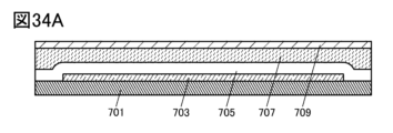
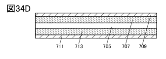
- an island-shaped peeling layer 703 is formed on a support substrate 701, and a peeled layer 705 is formed on the peeling layer 703.
- the support substrate 701 and a flexible substrate 709 are bonded together using an adhesive layer 707, and the adhesive layer 707 is cured ( Figure 34A).
- the support substrate 701 is a substrate having heat resistance that can withstand at least the processing temperatures during the manufacturing process.
- Examples of the support substrate 701 include a glass substrate, a quartz substrate, a sapphire substrate, a semiconductor substrate, a ceramic substrate, a metal substrate, a resin substrate, and a plastic substrate.
- an insulating film such as a silicon oxide film, a silicon oxynitride film, a silicon nitride film, or a silicon nitride oxide film as a base film between the support substrate 701 and the peeling layer 703, as this can prevent contamination from the support substrate 701.
- the peeling layer 703 can be formed in a single layer structure or a laminated structure using one or more of an element selected from tungsten, molybdenum, titanium, tantalum, niobium, nickel, cobalt, zirconium, zinc, ruthenium, rhodium, palladium, osmium, iridium, silicon, an alloy material containing the element, and a compound material containing the element.
- the crystal structure of the layer containing silicon may be amorphous, microcrystalline, or polycrystalline.
- a metal oxide such as aluminum oxide, gallium oxide, zinc oxide, titanium dioxide, indium oxide, indium tin oxide, indium zinc oxide, or In-Ga-Zn oxide may be used.
- the peeling layer 703 can be formed by, for example, a sputtering method, a plasma CVD method, a coating method (including a spin coating method, a droplet ejection method, a dispensing method, etc.), or a printing method.
- the thickness of the peeling layer 703 is preferably 10 nm or more and 200 nm or less, and more preferably 20 nm or more and 100 nm or less.
- a high melting point metal material such as tungsten, titanium, or molybdenum for the peeling layer 703 is preferable because it increases the degree of freedom in the process of forming the peeled layer 705.
- a tungsten layer, a molybdenum layer, a layer containing a mixture of tungsten and molybdenum, a layer containing an oxide or oxynitride of tungsten, a layer containing an oxide or oxynitride of molybdenum, or a layer containing an oxide or oxynitride of a mixture of tungsten and molybdenum may be formed.
- the mixture of tungsten and molybdenum corresponds to, for example, an alloy of tungsten and molybdenum.
- a layer containing an oxide of the metal may be formed by subjecting the surface of the layer containing the metal to thermal oxidation treatment, oxygen plasma treatment, nitrous oxide (N 2 O) plasma treatment, or treatment with a solution having a strong oxidizing power such as ozone water.
- the plasma treatment or heat treatment may be performed in an atmosphere of oxygen, nitrogen, or nitrous oxide alone, or a mixed gas of the gas and other gases.
- organic resin may be used as the release layer 703.
- organic resins include polyimide resin, acrylic resin, epoxy resin, polyamide resin, polyimideamide resin, siloxane resin, benzocyclobutene resin, and phenol resin.
- the insulating layer (first layer) formed in contact with the peeling layer 703 is preferably formed as a single layer or multiple layers using at least one of a silicon nitride film, a silicon oxynitride film, a silicon oxide film, and a silicon nitride oxide film.
- this is not limited thereto, and an optimal material can be selected depending on the material used for the peeling layer 703.
- curing adhesives for the adhesive layer 707, various types of curing adhesives can be used, such as photo-curing adhesives such as ultraviolet curing adhesives, reactive curing adhesives, heat curing adhesives, and anaerobic adhesives.
- these adhesives include epoxy resin, acrylic resin, silicone resin, phenolic resin, polyimide resin, imide resin, PVC resin, PVB resin, and EVA resin.
- materials with low moisture permeability such as epoxy resin are preferred.
- the adhesive it is preferable to use a material with low fluidity so that it can be placed only in the desired area.
- an adhesive sheet, a pressure-sensitive adhesive sheet, or a sheet- or film-shaped adhesive may be used.
- an OCA (optical clear adhesive) film can be preferably used.
- the resin may also contain a desiccant.
- a substance that adsorbs moisture by chemical adsorption such as an oxide of an alkaline earth metal (calcium oxide, barium oxide, etc.) may be used.
- a substance that adsorbs moisture by physical adsorption such as zeolite or silica gel, may be used.
- the inclusion of a desiccant is preferable because it can suppress deterioration of functional elements due to the intrusion of moisture from the atmosphere and improve the reliability of the device.
- the flexible substrate 709 may be made of polyester resins such as polyethylene terephthalate (PET) and polyethylene naphthalate (PEN), polyacrylonitrile resin, acrylic resin, polyimide resin, polymethyl methacrylate resin, polycarbonate (PC) resin, polyethersulfone (PES) resin, polyamide resin (nylon, aramid, etc.), polysiloxane resin, cycloolefin resin, polystyrene resin, polyamideimide resin, polyurethane resin, polyvinyl chloride resin, polyvinylidene chloride resin, polypropylene resin, polytetrafluoroethylene (PTFE) resin, ABS resin, cellulose nanofiber, etc.
- the substrate 709 may be made of various materials such as glass, quartz, resin, metal, alloy, or semiconductor (silicon, etc.) having a thickness sufficient to provide flexibility.
- a starting point for peeling may be formed first, and peeling may proceed from the starting point.
- the starting point for peeling may be formed by locally heating a part of the first layer or peeling layer 703 with laser light or the like, or by physically cutting or penetrating a part of the first layer or peeling layer 703 with a sharp member, or the like.
- the laser light is irradiated to the area where the cured adhesive layer 707, the layer to be peeled 705, and the peeling layer 703 overlap (see arrow P1 in Figure 34B).
- a starting point for peeling can be formed.
- other layers of the layer to be peeled 705, the peeling layer 703, and at least a portion of the adhesive layer 707 may also be removed.
- Substrate 711 can be made of the same material as that which can be used for substrate 709.
- the adhesive layer 713 can be made of the same material as that which can be used for the adhesive layer 707.
- a flexible device can be manufactured.
- a flexible display device can be manufactured.
- a method for producing a flexible device is to form an element layer on an inflexible substrate and then thin the substrate by polishing or other methods to make it flexible.
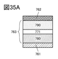
- the light-emitting device has an EL layer 763 between a pair of electrodes (a lower electrode 761 and an upper electrode 762).
- the EL layer 763 can be composed of multiple layers, such as a layer 780, a light-emitting layer 771, and a layer 790.
- the light-emitting layer 771 contains at least a light-emitting substance (also called a light-emitting material).
- the layer 780 has one or more of a layer containing a substance with high hole injection properties (hole injection layer), a layer containing a substance with high hole transport properties (hole transport layer), and a layer containing a substance with high electron blocking properties (electron block layer).
- the layer 790 has one or more of a layer containing a substance with high electron injection properties (electron injection layer), a layer containing a substance with high electron transport properties (electron transport layer), and a layer containing a substance with high hole blocking properties (hole block layer).
- the layers 780 and 790 have the opposite configurations to those described above.
- the structure having layer 780, light-emitting layer 771, and layer 790 disposed between a pair of electrodes can function as a single light-emitting unit, and in this specification, the structure in FIG. 35A is referred to as a single structure.
- FIG. 35B shows a modified example of the EL layer 763 of the light-emitting device shown in FIG. 35A.
- the light-emitting device shown in FIG. 35B has a layer 781 on the lower electrode 761, a layer 782 on the layer 781, a light-emitting layer 771 on the layer 782, a layer 791 on the light-emitting layer 771, a layer 792 on the layer 791, and an upper electrode 762 on the layer 792.
- the layer 781 can be a hole injection layer
- the layer 782 can be a hole transport layer
- the layer 791 can be an electron transport layer
- the layer 792 can be an electron injection layer.
- the layer 781 can be an electron injection layer
- the layer 782 can be an electron transport layer
- the layer 791 can be a hole transport layer
- the layer 792 can be a hole injection layer.
- a configuration in which multiple light-emitting layers (light-emitting layers 771, 772, 773) are provided between layer 780 and layer 790 is also a variation of the single structure.
- the light-emitting layer in a single-structure light-emitting device may have two layers, or may have four or more layers.
- a light-emitting device with a single structure may have a buffer layer between the two light-emitting layers.
- the buffer layer may be formed, for example, using a material that can be used for a hole transport layer or an electron transport layer.
- tandem structure a configuration in which multiple light-emitting units (light-emitting unit 763a and light-emitting unit 763b) are connected in series via a charge generation layer 785 (also referred to as an intermediate layer) is referred to as a tandem structure in this specification.
- the tandem structure may also be referred to as a stack structure.
- Figs. 35D and 35F are examples of a display device having a layer 764 that overlaps with the light-emitting device.
- Fig. 35D is an example in which layer 764 overlaps with the light-emitting device shown in Fig. 35C
- Fig. 35F is an example in which layer 764 overlaps with the light-emitting device shown in Fig. 35E.
- a conductive film that transmits visible light is used for the upper electrode 762 in order to extract light to the upper electrode 762 side.
- the light-emitting layers 771, 772, and 773 may be made of light-emitting materials that emit the same color of light, or may even be made of the same light-emitting material.
- the light-emitting layers 771, 772, and 773 may be made of light-emitting materials that emit blue light.
- the blue light emitted by the light-emitting device can be extracted.
- a color conversion layer is provided as the layer 764 shown in FIG. 35D, so that the blue light emitted by the light-emitting device can be converted into light with a longer wavelength, and red or green light can be extracted.
- both a color conversion layer and a colored layer as the layer 764.
- a part of the light emitted by the light-emitting device may be transmitted as it is without being converted by the color conversion layer.
- the colored layer can absorb light other than the desired color, and the color purity of the light emitted by the subpixel can be increased.
- light-emitting layers 771, 772, and 773 may each use a light-emitting material that emits light of a different color.
- the lights emitted by light-emitting layers 771, 772, and 773 are complementary colors, white light is obtained.
- a single-structure light-emitting device preferably has a light-emitting layer having a light-emitting material that emits blue light, and a light-emitting layer having a light-emitting material that emits visible light with a longer wavelength than blue light.
- a color filter as layer 764 shown in FIG. 35D. By transmitting white light through the color filter, light of the desired color can be obtained.
- a single-structure light-emitting device has three light-emitting layers
- a light-emitting layer having a light-emitting material that emits blue (B) light can be, for example, R, G, B from the anode side, or R, B, G from the anode side.
- a buffer layer may be provided between R and G or B.
- a configuration having a light-emitting layer containing a light-emitting material that emits blue (B) light and a light-emitting layer containing a light-emitting material that emits yellow (Y) light is preferable.
- This configuration is sometimes called a BY single structure.
- the light-emitting layers 771 and 772 may be made of light-emitting materials that emit the same color of light, or even the same light-emitting material.
- the light-emitting layers 771 and 772 may be made of light-emitting materials that emit blue light.
- the blue light emitted by the light-emitting device can be extracted.
- a color conversion layer can be provided as the layer 764 shown in FIG. 35F to convert the blue light emitted by the light-emitting device into light with a longer wavelength, and red or green light can be extracted.
- light-emitting layers 771 and 772 may each be made of a light-emitting material that emits light of a different color.
- white light can be obtained.
- Figures 35E and 35F show examples of light-emitting devices having two light-emitting units, this is not limiting.
- the light-emitting device may have three or more light-emitting units.
- a configuration having two light-emitting units may be referred to as a two-stage tandem structure, and a configuration having three light-emitting units may be referred to as a three-stage tandem structure.
- light-emitting unit 763a has layer 780a, light-emitting layer 771, and layer 790a
- light-emitting unit 763b has layer 780b, light-emitting layer 772, and layer 790b.
- the two light-emitting units are stacked via a charge generation layer 785.
- the charge generation layer 785 has at least a charge generation region.
- the charge generation layer 785 has the function of injecting electrons into one of the two light-emitting units and injecting holes into the other when a voltage is applied between a pair of electrodes.
- FIG. 36A to 36C An example of a light-emitting device with a tandem structure is shown in Figures 36A to 36C.
- FIG. 36A shows a configuration having three light-emitting units.
- a plurality of light-emitting units (light-emitting unit 763a, light-emitting unit 763b, and light-emitting unit 763c) are connected in series via charge generation layer 785.
- Light-emitting unit 763a has layer 780a, light-emitting layer 771, and layer 790a
- light-emitting unit 763b has layer 780b, light-emitting layer 772, and layer 790b
- light-emitting unit 763c has layer 780c, light-emitting layer 773, and layer 790c.
- layer 780c can use a configuration applicable to layers 780a and 780b
- layer 790c can use a configuration applicable to layers 790a and 790b.
- Fig. 36B shows a tandem-type light-emitting device in which light-emitting units having multiple light-emitting layers are stacked.
- two light-emitting units (light-emitting unit 763a and light-emitting unit 763b) are connected in series via charge generation layer 785.
- Light-emitting unit 763a has layer 780a, light-emitting layer 771a, light-emitting layer 771b, light-emitting layer 771c, and layer 790a
- light-emitting unit 763b has layer 780b, light-emitting layer 772a, light-emitting layer 772b, light-emitting layer 772c, and layer 790b.
- Emitting devices can be made using either low molecular weight compounds or high molecular weight compounds, and may contain inorganic compounds.
- the layers that make up the light emitting device can be formed by deposition methods (including vacuum deposition methods), transfer methods, printing methods, inkjet methods, coating methods, etc.
- Examples of phosphorescent materials include organometallic complexes (particularly iridium complexes) having a 4H-triazole skeleton, 1H-triazole skeleton, imidazole skeleton, pyrimidine skeleton, pyrazine skeleton, or pyridine skeleton, organometallic complexes (particularly iridium complexes) with a phenylpyridine derivative having an electron-withdrawing group as a ligand, platinum complexes, and rare earth metal complexes.
- organometallic complexes particularly iridium complexes having a 4H-triazole skeleton, 1H-triazole skeleton, imidazole skeleton, pyrimidine skeleton, pyrazine skeleton, or pyridine skeleton
- organometallic complexes (particularly iridium complexes) with a phenylpyridine derivative having an electron-withdrawing group as a ligand platinum complexe
- the electron blocking layer is provided in contact with the light emitting layer.
- the electron blocking layer is a layer containing a material that has hole transport properties and is capable of blocking electrons.
- the electron blocking layer can be made of any of the above hole transport materials that have electron blocking properties.
- the charge generation layer has at least a charge generation region.
- the charge generation region preferably contains an acceptor material, for example, a hole transport material and an acceptor material that are applicable to the hole injection layer described above.
- the electron injection buffer layer preferably contains an alkali metal or an alkaline earth metal, and may be configured to contain, for example, an alkali metal compound or an alkaline earth metal compound.
- the electron injection buffer layer preferably contains an inorganic compound containing an alkali metal and oxygen, or an inorganic compound containing an alkaline earth metal and oxygen, and more preferably contains an inorganic compound containing lithium and oxygen (lithium oxide (Li 2 O) or the like).
- the electron injection buffer layer may suitably use the above-mentioned materials applicable to the electron injection layer.
Landscapes
- Engineering & Computer Science (AREA)
- Physics & Mathematics (AREA)
- Multimedia (AREA)
- Signal Processing (AREA)
- Microelectronics & Electronic Packaging (AREA)
- General Physics & Mathematics (AREA)
- Optics & Photonics (AREA)
- Devices For Indicating Variable Information By Combining Individual Elements (AREA)
- Electroluminescent Light Sources (AREA)
Priority Applications (1)
| Application Number | Priority Date | Filing Date | Title |
|---|---|---|---|
| JP2024566920A JPWO2024141889A1 (https=) | 2022-12-28 | 2023-12-21 |
Applications Claiming Priority (2)
| Application Number | Priority Date | Filing Date | Title |
|---|---|---|---|
| JP2022211876 | 2022-12-28 | ||
| JP2022-211876 | 2022-12-28 |
Publications (1)
| Publication Number | Publication Date |
|---|---|
| WO2024141889A1 true WO2024141889A1 (ja) | 2024-07-04 |
Family
ID=91716603
Family Applications (1)
| Application Number | Title | Priority Date | Filing Date |
|---|---|---|---|
| PCT/IB2023/063068 Ceased WO2024141889A1 (ja) | 2022-12-28 | 2023-12-21 | 電子機器 |
Country Status (2)
| Country | Link |
|---|---|
| JP (1) | JPWO2024141889A1 (https=) |
| WO (1) | WO2024141889A1 (https=) |
Citations (3)
| Publication number | Priority date | Publication date | Assignee | Title |
|---|---|---|---|---|
| CN113301322A (zh) * | 2021-06-25 | 2021-08-24 | 上海锐像信息科技有限公司 | 一种vr眼镜及vr设备 |
| WO2022175776A1 (ja) * | 2021-02-18 | 2022-08-25 | 株式会社半導体エネルギー研究所 | 電子機器 |
| JP2022127597A (ja) * | 2021-02-19 | 2022-08-31 | 株式会社半導体エネルギー研究所 | 電子装置 |
-
2023
- 2023-12-21 JP JP2024566920A patent/JPWO2024141889A1/ja active Pending
- 2023-12-21 WO PCT/IB2023/063068 patent/WO2024141889A1/ja not_active Ceased
Patent Citations (3)
| Publication number | Priority date | Publication date | Assignee | Title |
|---|---|---|---|---|
| WO2022175776A1 (ja) * | 2021-02-18 | 2022-08-25 | 株式会社半導体エネルギー研究所 | 電子機器 |
| JP2022127597A (ja) * | 2021-02-19 | 2022-08-31 | 株式会社半導体エネルギー研究所 | 電子装置 |
| CN113301322A (zh) * | 2021-06-25 | 2021-08-24 | 上海锐像信息科技有限公司 | 一种vr眼镜及vr设备 |
Also Published As
| Publication number | Publication date |
|---|---|
| JPWO2024141889A1 (https=) | 2024-07-04 |
Similar Documents
| Publication | Publication Date | Title |
|---|---|---|
| JP2023093390A (ja) | 表示装置、及び電子機器 | |
| US20250037654A1 (en) | Electronic device | |
| JP2025118918A (ja) | 発光装置 | |
| JP2023016007A (ja) | 表示装置および電子装置 | |
| US20260065864A1 (en) | Electronic device | |
| KR20240004595A (ko) | 전자 기기 | |
| JP2026012332A (ja) | 眼鏡型またはゴーグル型の電子機器 | |
| CN120419310A (zh) | 半导体装置 | |
| JP7778722B2 (ja) | 表示システム | |
| JP7842118B2 (ja) | 表示装置、及び電子機器 | |
| WO2024141884A1 (ja) | 半導体装置、及び電子機器 | |
| CN120391099A (zh) | 半导体装置 | |
| WO2024141889A1 (ja) | 電子機器 | |
| KR20240095433A (ko) | 표시 장치 및 전자 기기 | |
| CN118076993A (zh) | 电子设备 | |
| CN118235194A (zh) | 电子设备 | |
| US12416970B2 (en) | Electronic device and operation method of the electronic device | |
| US20240431178A1 (en) | Display Apparatus, Electronic Device, And Operation Method Of Light-Emitting Apparatus | |
| JP2025139661A (ja) | 表示装置、画像データの処理方法 | |
| TW202433434A (zh) | 顯示裝置 | |
| WO2024176038A1 (ja) | 表示システム | |
| CN118160027A (zh) | 显示装置及电子设备 | |
| WO2026058121A1 (ja) | 表示装置、及び表示装置の作製方法 | |
| CN117581289A (zh) | 电子设备 | |
| WO2026058127A1 (ja) | 表示装置及び表示装置の作製方法 |
Legal Events
| Date | Code | Title | Description |
|---|---|---|---|
| 121 | Ep: the epo has been informed by wipo that ep was designated in this application |
Ref document number: 23911087 Country of ref document: EP Kind code of ref document: A1 |
|
| WWE | Wipo information: entry into national phase |
Ref document number: 2024566920 Country of ref document: JP |
|
| NENP | Non-entry into the national phase |
Ref country code: DE |
|
| 122 | Ep: pct application non-entry in european phase |
Ref document number: 23911087 Country of ref document: EP Kind code of ref document: A1 |