WO2024141880A1 - 発光デバイス - Google Patents
発光デバイス Download PDFInfo
- Publication number
- WO2024141880A1 WO2024141880A1 PCT/IB2023/063058 IB2023063058W WO2024141880A1 WO 2024141880 A1 WO2024141880 A1 WO 2024141880A1 IB 2023063058 W IB2023063058 W IB 2023063058W WO 2024141880 A1 WO2024141880 A1 WO 2024141880A1
- Authority
- WO
- WIPO (PCT)
- Prior art keywords
- light
- layer
- electrode
- emitting device
- abbreviation
- Prior art date
- Legal status (The legal status is an assumption and is not a legal conclusion. Google has not performed a legal analysis and makes no representation as to the accuracy of the status listed.)
- Ceased
Links
Images
































Classifications
-
- H—ELECTRICITY
- H10—SEMICONDUCTOR DEVICES; ELECTRIC SOLID-STATE DEVICES NOT OTHERWISE PROVIDED FOR
- H10K—ORGANIC ELECTRIC SOLID-STATE DEVICES
- H10K71/00—Manufacture or treatment specially adapted for the organic devices covered by this subclass
- H10K71/20—Changing the shape of the active layer in the devices, e.g. patterning
- H10K71/231—Changing the shape of the active layer in the devices, e.g. patterning by etching of existing layers
- H10K71/233—Changing the shape of the active layer in the devices, e.g. patterning by etching of existing layers by photolithographic etching
-
- G—PHYSICS
- G09—EDUCATION; CRYPTOGRAPHY; DISPLAY; ADVERTISING; SEALS
- G09F—DISPLAYING; ADVERTISING; SIGNS; LABELS OR NAME-PLATES; SEALS
- G09F9/00—Indicating arrangements for variable information in which the information is built-up on a support by selection or combination of individual elements
- G09F9/30—Indicating arrangements for variable information in which the information is built-up on a support by selection or combination of individual elements in which the desired character or characters are formed by combining individual elements
- G09F9/301—Indicating arrangements for variable information in which the information is built-up on a support by selection or combination of individual elements in which the desired character or characters are formed by combining individual elements flexible foldable or roll-able electronic displays, e.g. thin LCD, OLED
-
- H—ELECTRICITY
- H10—SEMICONDUCTOR DEVICES; ELECTRIC SOLID-STATE DEVICES NOT OTHERWISE PROVIDED FOR
- H10K—ORGANIC ELECTRIC SOLID-STATE DEVICES
- H10K50/00—Organic light-emitting devices
- H10K50/10—OLEDs or polymer light-emitting diodes [PLED]
- H10K50/11—OLEDs or polymer light-emitting diodes [PLED] characterised by the electroluminescent [EL] layers
- H10K50/12—OLEDs or polymer light-emitting diodes [PLED] characterised by the electroluminescent [EL] layers comprising dopants
-
- H—ELECTRICITY
- H10—SEMICONDUCTOR DEVICES; ELECTRIC SOLID-STATE DEVICES NOT OTHERWISE PROVIDED FOR
- H10K—ORGANIC ELECTRIC SOLID-STATE DEVICES
- H10K59/00—Integrated devices, or assemblies of multiple devices, comprising at least one organic light-emitting element covered by group H10K50/00
- H10K59/10—OLED displays
- H10K59/12—Active-matrix OLED [AMOLED] displays
- H10K59/122—Pixel-defining structures or layers, e.g. banks
-
- H—ELECTRICITY
- H10—SEMICONDUCTOR DEVICES; ELECTRIC SOLID-STATE DEVICES NOT OTHERWISE PROVIDED FOR
- H10K—ORGANIC ELECTRIC SOLID-STATE DEVICES
- H10K85/00—Organic materials used in the body or electrodes of devices covered by this subclass
- H10K85/30—Coordination compounds
-
- H—ELECTRICITY
- H10—SEMICONDUCTOR DEVICES; ELECTRIC SOLID-STATE DEVICES NOT OTHERWISE PROVIDED FOR
- H10K—ORGANIC ELECTRIC SOLID-STATE DEVICES
- H10K85/00—Organic materials used in the body or electrodes of devices covered by this subclass
- H10K85/30—Coordination compounds
- H10K85/341—Transition metal complexes, e.g. Ru(II)polypyridine complexes
- H10K85/342—Transition metal complexes, e.g. Ru(II)polypyridine complexes comprising iridium
-
- H—ELECTRICITY
- H10—SEMICONDUCTOR DEVICES; ELECTRIC SOLID-STATE DEVICES NOT OTHERWISE PROVIDED FOR
- H10K—ORGANIC ELECTRIC SOLID-STATE DEVICES
- H10K85/00—Organic materials used in the body or electrodes of devices covered by this subclass
- H10K85/60—Organic compounds having low molecular weight
- H10K85/631—Amine compounds having at least two aryl rest on at least one amine-nitrogen atom, e.g. triphenylamine
- H10K85/633—Amine compounds having at least two aryl rest on at least one amine-nitrogen atom, e.g. triphenylamine comprising polycyclic condensed aromatic hydrocarbons as substituents on the nitrogen atom
-
- H—ELECTRICITY
- H10—SEMICONDUCTOR DEVICES; ELECTRIC SOLID-STATE DEVICES NOT OTHERWISE PROVIDED FOR
- H10K—ORGANIC ELECTRIC SOLID-STATE DEVICES
- H10K85/00—Organic materials used in the body or electrodes of devices covered by this subclass
- H10K85/60—Organic compounds having low molecular weight
- H10K85/631—Amine compounds having at least two aryl rest on at least one amine-nitrogen atom, e.g. triphenylamine
- H10K85/636—Amine compounds having at least two aryl rest on at least one amine-nitrogen atom, e.g. triphenylamine comprising heteroaromatic hydrocarbons as substituents on the nitrogen atom
-
- H—ELECTRICITY
- H10—SEMICONDUCTOR DEVICES; ELECTRIC SOLID-STATE DEVICES NOT OTHERWISE PROVIDED FOR
- H10K—ORGANIC ELECTRIC SOLID-STATE DEVICES
- H10K85/00—Organic materials used in the body or electrodes of devices covered by this subclass
- H10K85/60—Organic compounds having low molecular weight
- H10K85/649—Aromatic compounds comprising a hetero atom
- H10K85/654—Aromatic compounds comprising a hetero atom comprising only nitrogen as heteroatom
-
- H—ELECTRICITY
- H10—SEMICONDUCTOR DEVICES; ELECTRIC SOLID-STATE DEVICES NOT OTHERWISE PROVIDED FOR
- H10K—ORGANIC ELECTRIC SOLID-STATE DEVICES
- H10K85/00—Organic materials used in the body or electrodes of devices covered by this subclass
- H10K85/60—Organic compounds having low molecular weight
- H10K85/649—Aromatic compounds comprising a hetero atom
- H10K85/657—Polycyclic condensed heteroaromatic hydrocarbons
-
- H—ELECTRICITY
- H10—SEMICONDUCTOR DEVICES; ELECTRIC SOLID-STATE DEVICES NOT OTHERWISE PROVIDED FOR
- H10K—ORGANIC ELECTRIC SOLID-STATE DEVICES
- H10K85/00—Organic materials used in the body or electrodes of devices covered by this subclass
- H10K85/60—Organic compounds having low molecular weight
- H10K85/649—Aromatic compounds comprising a hetero atom
- H10K85/657—Polycyclic condensed heteroaromatic hydrocarbons
- H10K85/6572—Polycyclic condensed heteroaromatic hydrocarbons comprising only nitrogen in the heteroaromatic polycondensed ring system, e.g. phenanthroline or carbazole
-
- H—ELECTRICITY
- H10—SEMICONDUCTOR DEVICES; ELECTRIC SOLID-STATE DEVICES NOT OTHERWISE PROVIDED FOR
- H10K—ORGANIC ELECTRIC SOLID-STATE DEVICES
- H10K85/00—Organic materials used in the body or electrodes of devices covered by this subclass
- H10K85/60—Organic compounds having low molecular weight
- H10K85/649—Aromatic compounds comprising a hetero atom
- H10K85/657—Polycyclic condensed heteroaromatic hydrocarbons
- H10K85/6574—Polycyclic condensed heteroaromatic hydrocarbons comprising only oxygen in the heteroaromatic polycondensed ring system, e.g. cumarine dyes
-
- H—ELECTRICITY
- H10—SEMICONDUCTOR DEVICES; ELECTRIC SOLID-STATE DEVICES NOT OTHERWISE PROVIDED FOR
- H10K—ORGANIC ELECTRIC SOLID-STATE DEVICES
- H10K85/00—Organic materials used in the body or electrodes of devices covered by this subclass
- H10K85/60—Organic compounds having low molecular weight
- H10K85/649—Aromatic compounds comprising a hetero atom
- H10K85/657—Polycyclic condensed heteroaromatic hydrocarbons
- H10K85/6576—Polycyclic condensed heteroaromatic hydrocarbons comprising only sulfur in the heteroaromatic polycondensed ring system, e.g. benzothiophene
-
- H—ELECTRICITY
- H10—SEMICONDUCTOR DEVICES; ELECTRIC SOLID-STATE DEVICES NOT OTHERWISE PROVIDED FOR
- H10K—ORGANIC ELECTRIC SOLID-STATE DEVICES
- H10K2101/00—Properties of the organic materials covered by group H10K85/00
- H10K2101/20—Delayed fluorescence emission
-
- H—ELECTRICITY
- H10—SEMICONDUCTOR DEVICES; ELECTRIC SOLID-STATE DEVICES NOT OTHERWISE PROVIDED FOR
- H10K—ORGANIC ELECTRIC SOLID-STATE DEVICES
- H10K2101/00—Properties of the organic materials covered by group H10K85/00
- H10K2101/20—Delayed fluorescence emission
- H10K2101/25—Delayed fluorescence emission using exciplex
Definitions
- One aspect of the present invention relates to a light-emitting device.
- Display devices have been developed for a variety of applications in recent years.
- applications of large display devices include home television devices (also called televisions or television receivers), digital signage, and PIDs (Public Information Displays), while the development of applications of small display devices includes smartphones and tablet terminals equipped with touch panels.
- Another object of one embodiment of the present invention is to provide a light-emitting device that can be arranged at high density and has good reliability.
- Another object of one embodiment of the present invention is to provide a light-emitting device that can provide a high-definition display device and has good reliability.
- one object of one embodiment of the present invention is to provide a display device with high display performance.
- one object of one embodiment of the present invention is to provide a display device with high resolution and good display performance.
- one object of one embodiment of the present invention is to provide a display device with good display quality and good display performance.
- a light-emitting device is one of a plurality of light-emitting devices included in a light-emitting device group having a first electrode group formed on the same insulating surface, a second electrode facing the first electrode group, and a first layer group located between the first electrode group and the second electrode, wherein the first electrode group is made of a plurality of first electrodes that are independent in each of the plurality of light-emitting devices, the first layer group is made of a plurality of first layers that are independent in each of the plurality of light-emitting devices, and the second electrode is a continuous conductive layer shared by the plurality of light-emitting devices,
- the light-emitting device has a first electrode that is one of the first electrode group, the second electrode, and a first layer that is one of the first layer group, the second electrode and the first layer overlap the first electrode, the first layer has a light-emitting layer that includes a luminescent center substance and a first substance, the wavelength of
- another aspect of the present invention is a light-emitting device among a plurality of light-emitting devices included in a light-emitting device group having a first electrode group formed on the same insulating surface, a second electrode facing the first electrode group, and a first layer group located between the first electrode group and the second electrode, wherein the first electrode group is made of a plurality of first electrodes that are independent in each of the plurality of light-emitting devices, the first layer group is made of a plurality of first layers that are independent in each of the plurality of light-emitting devices, and the second electrode is a layer shared by the plurality of light-emitting devices.
- the light-emitting device is a continuous conductive layer, and the light-emitting device has a first electrode that is one of the first electrode group, the second electrode, and a first layer that is one of the first layer group, the second electrode and the first layer overlap the first electrode, the first layer has a light-emitting layer that includes a light-emitting center substance and a first substance, the first substance does not include a fused ring that is composed only of a six-membered ring, and the distance between the first layer of the light-emitting device and the first layer of another light-emitting device adjacent to the light-emitting device is 2 ⁇ m or more and 5 ⁇ m or less.
- another aspect of the present invention is a light-emitting device among a plurality of light-emitting devices included in a light-emitting device group having a first electrode group formed on the same insulating surface, a second electrode facing the first electrode group, and a first layer group located between the first electrode group and the second electrode, wherein the first electrode group is made of a plurality of first electrodes that are independent in each of the plurality of light-emitting devices, the first layer group is made of a plurality of first layers that are independent in each of the plurality of light-emitting devices, the second electrode is a continuous conductive layer shared by the plurality of light-emitting devices, and the light-emitting device is one of the plurality of light-emitting devices including the first electrode group, the second electrode facing the first electrode group, and the second layer group is made of a plurality of first layers that are independent in each of the plurality of light-emitting devices,
- the light-emitting device has a first electrode that is one of
- another aspect of the present invention is a light-emitting device among a plurality of light-emitting devices included in a light-emitting device group having a first electrode group formed on the same insulating surface, a second electrode facing the first electrode group, and a first layer group located between the first electrode group and the second electrode, wherein the first electrode group is made of a plurality of first electrodes that are independent in each of the plurality of light-emitting devices, the first layer group is made of a plurality of first layers that are independent in each of the plurality of light-emitting devices, and the second electrode is a light-emitting device among a plurality of light-emitting devices included in a light-emitting device group having a first electrode group formed on the same insulating surface, a second electrode facing the first electrode group, and a first layer group located between the first electrode group and the second electrode, wherein the first electrode group is made of a plurality of first electrodes that are independent in each of the plurality of light-
- the light-emitting device has a first electrode that is one of the first electrode group, the second electrode, and a first layer that is one of the first layer group, the second electrode and the first layer overlap the first electrode, the first layer has a light-emitting layer that includes a light-emitting center substance and a first substance, the first substance does not include any of a naphthalene ring, a phenanthrene ring, and a naphthacene ring, and the distance between the first layer of the light-emitting device and the first layer of another light-emitting device adjacent to the light-emitting device is 2 ⁇ m or more and 5 ⁇ m or less.
- another aspect of the present invention is a light-emitting device among a plurality of light-emitting devices included in a light-emitting device group having a first electrode group formed on the same insulating surface, a second electrode facing the first electrode group, and a first layer group located between the first electrode group and the second electrode, wherein the first electrode group is made of a plurality of first electrodes that are independent in each of the plurality of light-emitting devices, the first layer group is made of a plurality of first layers that are independent in each of the plurality of light-emitting devices, and the second electrode is a continuous conductive layer shared by the plurality of light-emitting devices.
- the light-emitting device has a first electrode that is one of the first electrode group, the second electrode, and a first layer that is one of the first layer group, the second electrode and the first layer overlap the first electrode, the first layer has a light-emitting layer containing a light-emitting center substance and a first substance, the first substance has a condensed ring, and the condensed ring is an alternating condensation of a six-membered ring and a five-membered ring, and the distance between the first layer of the light-emitting device and the first layer of another light-emitting device adjacent to the light-emitting device is 2 ⁇ m or more and 5 ⁇ m or less.
- another aspect of the present invention is a light-emitting device having the above configuration, in which the wavelength of the absorption edge located at the longest wavelength in the absorption spectrum of the light-emitting substance is 400 nm or longer.
- another aspect of the present invention is a light-emitting device having the above configuration, in which the light-emitting material absorbs light having a wavelength of 400 nm or more and 475 nm or less.
- another aspect of the present invention is a light-emitting device having the above configuration, in which the first layer contains a second material, and the second material has a structure having the same characteristics as those described as the structural characteristics of the first material.
- another aspect of the present invention is a light-emitting device having the above configuration, in which the first layer contains a second substance, and the wavelength of the absorption edge located at the longest wavelength in the absorption spectrum of the second substance is less than 400 nm.
- another aspect of the present invention is a light-emitting device having the above configuration, in which the first layer contains a second material, and the second material does not contain a naphthalene structure.
- another aspect of the present invention is a light-emitting device having the above configuration, in which one of the first substance and the second substance is an organic compound having a ⁇ -electron rich heteroaromatic ring, and the other is an organic compound having a ⁇ -electron deficient heteroaromatic ring skeleton.
- another aspect of the present invention is a light-emitting device having the above configuration, in which the light-emitting substance exhibits thermally activated delayed fluorescence.
- another aspect of the present invention is a light-emitting device having the above configuration, in which the light-emitting material emits light having a spectral peak at 500 nm or less.
- a highly reliable display device can be provided.
- a display device with high resolution and good display performance can be provided.
- a display device with good display quality and good display performance can be provided.
- FIGS. 1A-1C are diagrams illustrating a light emitting device.
- FIG. 2 is a diagram illustrating a light emitting device.
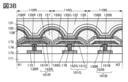
- 3A and 3B are a top view and a cross-sectional view of a light emitting device.
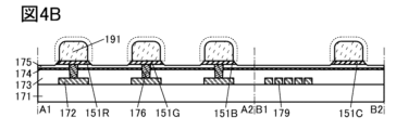
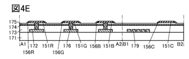
- 4A to 4E are cross-sectional views showing an example of a method for manufacturing a display device.
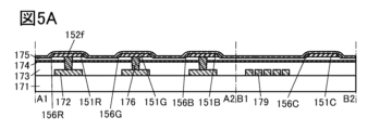
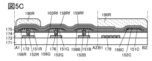
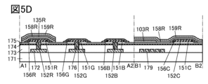
- 5A to 5D are cross-sectional views showing an example of a method for manufacturing a display device.
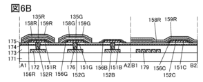
- 6A to 6D are cross-sectional views showing an example of a method for manufacturing a display device.
- 7A to 7C are cross-sectional views showing an example of a method for manufacturing a display device.
- 8A to 8C are cross-sectional views showing an example of a method for manufacturing a display device.
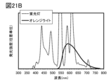
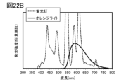
- FIG. 22A shows the absorption spectrum of the organic compound used in the light-emitting layer of the light-emitting device 4, and FIG. 22B shows the emission spectrum of a fluorescent lamp and that of orange light.
- 23A to 23D are diagrams showing the initial characteristics of the light-emitting device 1.
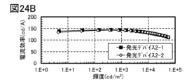
- FIG. 24A to 24D are diagrams showing the initial characteristics of the light emitting device 2.
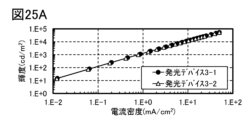
- FIG. 25A to 25D are diagrams showing the initial characteristics of the light emitting device 3.
- FIG. 26A to 26D are diagrams showing the initial characteristics of the light emitting device 4.
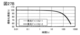
- FIG. 27A to 27D are diagrams showing changes in luminance with respect to the driving time of light-emitting devices 1 to 4.
- a device fabricated using a metal mask or an FMM may be referred to as a device with an MM (metal mask) structure.
- a device fabricated without using a metal mask or an FMM may be referred to as a device with an MML (metal maskless) structure.
- white light is usually used for illumination, and white light almost always contains short-wavelength components of 475 nm or less. Therefore, by taking measures to replace the lamps that emit white light with lights that do not contain light with wavelengths of 475 nm or less, such as orange lights, it becomes possible to process light-emitting devices using the photolithography process without generating impurities (deterioration products), but this requires a certain amount of capital investment. Furthermore, illumination that blocks short-wavelength components reduces visibility, and there is a risk that problems may be easily overlooked.
- the luminescent material absorbs high-energy light with a wavelength of 400 nm to 475 nm, as long as the host material does not absorb high-energy light with a wavelength of 400 nm to 475 nm, a light-emitting device in which deterioration is suppressed even when exposed to the atmosphere under white lighting such as a fluorescent lamp or a white LED can be provided.
- the difference in wavelength between the absorption ends located at the longest wavelength among the absorption ends in the absorption spectrum of the host material and the absorption ends in the absorption spectrum of the luminescent material is preferably 60 nm or more.
- the molar absorption coefficient of the light-emitting substance at a wavelength of 400 nm or more and 475 nm or less may be 1000 M ⁇ 1 ⁇ cm ⁇ 1 or more, 2000 M ⁇ 1 ⁇ cm ⁇ 1 or more, 5000 M ⁇ 1 ⁇ cm ⁇ 1 or more, or 10000 M ⁇ 1 ⁇ cm ⁇ 1 or more.
- the second host material is preferably an organic compound having an absorption edge located at the longest wavelength of the absorption edges in the absorption spectrum at less than 400 nm, similar to the above-mentioned host material.
- the second host material does not absorb high-energy light having a wavelength of 400 nm to 475 nm.
- the molecular structure of the second host material does not include a fused aromatic ring composed only of six-membered rings.
- organic compounds containing a heteroaromatic ring having a diazine (pyrimidine or pyrazine) skeleton and organic compounds containing a heteroaromatic ring having a triazine skeleton are preferred because they have high electron transport properties and contribute to reducing the driving voltage.
- the anode is preferably formed using a metal, alloy, conductive compound, or mixture thereof with a large work function (specifically, 4.0 eV or more).
- a metal, alloy, conductive compound, or mixture thereof with a large work function specifically, 4.0 eV or more.
- Specific examples include indium oxide-tin oxide (ITO), indium oxide-tin oxide containing silicon or silicon oxide (ITSO), indium oxide-zinc oxide, and indium oxide containing tungsten oxide and zinc oxide (IWZO).
- ITO indium oxide-tin oxide
- ITSO indium oxide-tin oxide containing silicon or silicon oxide
- IWZO indium oxide containing tungsten oxide and zinc oxide
- These conductive metal oxide films are usually formed by sputtering, but may also be formed by applying a sol-gel method.
- a method for forming indium oxide-zinc oxide a method of forming the film by sputtering using a target in which 1 to 20 wt % zinc oxide
- organic compound having hole transport properties used in the composite material various organic compounds such as aromatic amine compounds, heteroaromatic compounds, aromatic hydrocarbons, and polymeric compounds (oligomers, dendrimers, polymers, etc.) can be used.
- organic compound having hole transport properties used in the composite material it is preferable that it is an organic compound having a hole mobility of 1 ⁇ 10 ⁇ 6 cm 2 /Vs or more.
- the organic compound having hole transport properties used in the composite material is a compound having a condensed aromatic hydrocarbon ring or a ⁇ -electron-rich heteroaromatic ring.
- condensed aromatic hydrocarbon ring an anthracene ring, a naphthalene ring, etc.
- the ⁇ -electron-rich heteroaromatic ring it is preferable that it is a condensed aromatic ring containing at least one of a pyrrole skeleton, a furan skeleton, and a thiophene skeleton in the ring, and specifically, it is preferable that it is a carbazole ring, a dibenzothiophene ring, or a ring in which an aromatic ring or a heteroaromatic ring is further condensed to them.
- Organometallic iridium complexes having a 4H-triazole skeleton such as tris ⁇ 2-[5-(2-methylphenyl)-4-(2,6-dimethylphenyl)-4H-1,2,4-triazol-3-yl- ⁇ N2]phenyl- ⁇ C ⁇ iridium(III) (abbreviation: [Ir(mpptz-dmp) 3 ]), tris(5-methyl-3,4-diphenyl-4H-1,2,4-triazolato)iridium(III) (abbreviation: [Ir(Mptz) 3 ]), and tris[3-methyl-1-(2-methylphenyl)-5-phenyl-1H-1,2,4-triazolato]iridium(III) (abbreviation: [Ir(Mptz1-mp) 3 ]).
- organometallic iridium complexes having a pyrimidine skeleton are particularly preferred because they are also remarkably excellent in reliability or luminous efficiency.
- organometallic iridium complexes having a pyridine skeleton such as [ru- ⁇ C]iridium(III)
- platinum complexes such as 2,3,7,8,12,13,17,18-octaethyl-21H,23H-porphyrin platinum(II) (abbreviation: PtOEP)
- rare earth metal complexes such as tris(1,3-diphenyl-1,3-propanedionato)(monophenanthroline)europium(III) (abbreviation: [Eu(DBM) 3 (Phen)]) and tris[1-(2-thenoyl)-3,3,3-trifluoroacetonato](monophenanthroline)europium(III) (abbreviation: [Eu(TTA) 3 (Phen)])
- PtOEP platinum complexes
- rare earth metal complexes such as tris(1,3-diphenyl-1,3-prop
- known phosphorescent compounds may be selected and used.
- TADF materials examples include fullerene and its derivatives, acridine and its derivatives, eosin derivatives, etc. Also included are metal-containing porphyrins that contain magnesium (Mg), zinc (Zn), cadmium (Cd), tin (Sn), platinum (Pt), indium (In), palladium (Pd), etc.
- Mg magnesium
- Zn zinc
- Cd cadmium
- Sn tin
- Pt platinum
- In indium
- Pd palladium
- metal-containing porphyrin examples include protoporphyrin-tin fluoride complex ( SnF2 (Proto IX)), mesoporphyrin-tin fluoride complex ( SnF2 (Meso IX)), hematoporphyrin-tin fluoride complex ( SnF2 (Hemato IX)), coproporphyrin tetramethyl ester-tin fluoride complex ( SnF2 (Copro III-4Me)), octaethylporphyrin-tin fluoride complex ( SnF2 (OEP)), etioporphyrin-tin fluoride complex ( SnF2 (Etio I)), and octaethylporphyrin-platinum chloride complex ( PtCl2 OEP), which are shown in the following structural formulas.
- the heterocyclic compound has a ⁇ -electron rich heteroaromatic ring and a ⁇ -electron deficient heteroaromatic ring, and therefore has high electron transport and hole transport properties, and is therefore preferred.
- the skeletons having a ⁇ -electron deficient heteroaromatic ring the pyridine skeleton, the diazine skeleton (pyrimidine skeleton, pyrazine skeleton, pyridazine skeleton), and the triazine skeleton are preferred because they are stable and reliable.
- the benzofuropyrimidine skeleton, the benzothienopyrimidine skeleton, the benzofuropyrazine skeleton, and the benzothienopyrazine skeleton are preferred because they have high acceptor properties and good reliability.
- the skeletons having a ⁇ -electron rich heteroaromatic ring are preferred because they are stable and reliable, and therefore at least one of these skeletons is preferred.
- a material having electron transport properties and/or a material having hole transport properties as described in embodiment 1 can be used as the host material of the light-emitting layer.
- a material that satisfies the conditions shown in embodiment 1, such as the TADF material described above, can be used.
- various carrier transport materials can be used as long as they satisfy the conditions shown in embodiment 1.
- At least one of the materials forming the exciplex may be a phosphorescent material. This allows the triplet excitation energy to be efficiently converted into singlet excitation energy by reverse intersystem crossing.
- the HOMO level of the material having hole transport properties is equal to or higher than the HOMO level of the material having electron transport properties. It is also preferable that the LUMO level of the material having hole transport properties is equal to or higher than the LUMO level of the material having electron transport properties.
- the LUMO level and HOMO level of the material can be derived from the electrochemical properties (reduction potential and oxidation potential) of the material measured by cyclic voltammetry (CV) measurement.
- transient photoluminescence (PL) of a material having hole transport properties the transient PL of a material having electron transport properties, and the transient PL of a mixed film obtained by mixing these materials, and observing the difference in transient response, such as the transient PL lifetime of the mixed film having a longer lifetime component than the transient PL lifetime of each material, or the proportion of delayed components becoming larger.
- the above-mentioned transient PL may be read as transient electroluminescence (EL).
- the formation of an exciplex can also be confirmed by comparing the transient EL of a material having hole transport properties, the transient EL of a material having electron transport properties, and the transient EL of a mixed film obtained by mixing these materials, and observing the difference in transient response.
- the electron transport layer 114 is a layer containing a substance having electron transport properties.
- a substance having an electron mobility of 1 ⁇ 10 ⁇ 7 cm 2 /Vs or more, preferably 1 ⁇ 10 ⁇ 6 cm 2 /Vs or more at a square root of an electric field strength [V/cm] of 600 is preferable. Note that other substances can be used as long as they have a higher electron transport property than holes.
- an organic compound having a ⁇ -electron deficient heteroaromatic ring skeleton is preferable.
- organic compounds containing a heteroaromatic ring having a diazine skeleton (pyrimidine skeleton, pyrazine skeleton, pyridazine skeleton), organic compounds containing a heteroaromatic ring having a pyridine skeleton, and organic compounds containing a heteroaromatic ring having a triazine skeleton are preferable because of their good reliability.
- organic compounds containing a heteroaromatic ring having a diazine (pyrimidine or pyrazine) skeleton and organic compounds containing a heteroaromatic ring having a triazine skeleton have high electron transport properties and contribute to reducing the driving voltage.
- benzofuropyrimidine skeleton benzothienopyrimidine skeleton, benzofuropyrazine skeleton, and benzothienopyrazine skeleton are preferable because of their high acceptor properties and good reliability.
- organic compounds containing a heteroaromatic ring having a diazine skeleton, organic compounds containing a heteroaromatic ring having a pyridine skeleton, and organic compounds containing a heteroaromatic ring having a triazine skeleton are preferred because they have good reliability.
- organic compounds containing a heteroaromatic ring having a diazine (pyrimidine or pyrazine) skeleton and organic compounds containing a heteroaromatic ring having a triazine skeleton are preferred because they have high electron transport properties and contribute to reducing the driving voltage.
- organic compounds having a phenanthroline skeleton such as mTpPPhen, PnNPhen, and mPPhen2P are preferred, and organic compounds having a phenanthroline dimer structure such as mPPhen2P are more preferred because they have excellent stability.
- the electron transport layer 114 may have a laminated structure.
- a layer in the electron transport layer 114 having a laminated structure that is in contact with the light-emitting layer 113 may function as a hole blocking layer.
- a layer containing an alkali metal or alkaline earth metal compound or complex such as lithium fluoride, 8-hydroxyquinolinato-lithium (abbreviation: Liq), a mixed material of lithium fluoride and ytterbium, or a mixture thereof or 1,1'-pyridine-2,6-diyl-bis(1,3,4,6,7,8-hexahydro-2H-pyrimido[1,2-a]pyrimidine) (abbreviation: hpp2Py), etc.
- Liq lithium fluoride, 8-hydroxyquinolinato-lithium
- hpp2Py 1,1'-pyridine-2,6-diyl-bis(1,3,4,6,7,8-hexahydro-2H-pyrimido[1,2-a]pyrimidine)
- a charge generation layer 116 may be provided instead of the electron injection layer 115 (FIG. 1B).
- the charge generation layer 116 is a layer that can inject holes into a layer in contact with the cathode side of the layer and electrons into a layer in contact with the anode side of the layer by applying a potential.
- the charge generation layer 116 includes at least a P-type layer 117.
- the P-type layer 117 is preferably formed using the composite material listed as a material that can form the hole injection layer 111 described above.
- the P-type layer 117 may also be formed by laminating a film containing the acceptor material described above as a material that forms the composite material and a film containing a hole transport material.
- the organic compound of one embodiment of the present invention is an organic compound with a low refractive index, by using it for the P-type layer 117, an organic EL element with good external quantum efficiency can be obtained.
- the charge generation layer 116 has one or both of an electron relay layer 118 and an electron injection buffer layer 119 in addition to the P-type layer 117.
- the electron injection buffer layer 119 can be made of a material with high electron injection properties, such as alkali metals, alkaline earth metals, rare earth metals, and their compounds (alkali metal compounds (including oxides such as lithium oxide, halides such as lithium fluoride, and carbonates such as lithium carbonate and cesium carbonate), alkaline earth metal compounds (including oxides, halides, and carbonates), or rare earth metal compounds (including oxides, halides, and carbonates)).
- alkali metal compounds including oxides such as lithium oxide, halides such as lithium fluoride, and carbonates such as lithium carbonate and cesium carbonate
- alkaline earth metal compounds including oxides, halides, and carbonates
- rare earth metal compounds including oxides, halides, and carbonates
- the donor substance may be an alkali metal, an alkaline earth metal, a rare earth metal, or a compound thereof (an alkali metal compound (including an oxide such as lithium oxide, a halide such as lithium fluoride, or a carbonate such as lithium carbonate or cesium carbonate), an alkaline earth metal compound (including an oxide, a halide, or a carbonate), or a rare earth metal compound (including an oxide, a halide, or a carbonate)), or an organic compound such as tetrathianaphthacene (abbreviation: TTN), nickelocene, or decamethylnickelocene.
- TTN tetrathianaphthacene
- nickelocene nickelocene
- decamethylnickelocene the substance having electron transport properties may be formed using a material similar to the material constituting the electron transport layer 114 described above.
- the second electrode 102 is an electrode including a cathode.
- the second electrode 102 may have a laminated structure, in which case the layer in contact with the organic compound layer 103 functions as the cathode.
- a material for forming the cathode a metal, an alloy, an electrically conductive compound, and a mixture thereof having a small work function (specifically, 3.8 eV or less) can be used.
- the electron injection layer 115 or a thin film of the above-mentioned material having a small work function between the second electrode 102 and the electron transport layer various conductive materials such as Al, Ag, ITO, indium oxide-tin oxide containing silicon or silicon oxide can be used as the cathode regardless of the magnitude of the work function.
- the second electrode 102 is made of a material that is transparent to visible light, a light-emitting device that emits light from the second electrode 102 side can be obtained.
- These conductive materials can be formed into films using dry methods such as vacuum deposition or sputtering, inkjet methods, spin coating methods, etc. They may also be formed using a wet method using a sol-gel method, or a wet method using a paste of a metal material.
- each of the electrodes or layers described above may be formed using a different film formation method.
- a first light-emitting unit 511 and a second light-emitting unit 512 are stacked between a first electrode 501 and a second electrode 502, and a charge generation layer 513 is provided between the first light-emitting unit 511 and the second light-emitting unit 512.
- the first electrode 501 and the second electrode 502 correspond to the first electrode 101 and the second electrode 102 in FIG. 1A, respectively, and the same as those described in the description of FIG. 1A can be applied.
- the first light-emitting unit 511 and the second light-emitting unit 512 may have the same configuration or different configurations.
- the charge generation layer 513 has a function of injecting electrons into one light-emitting unit and injecting holes into the other light-emitting unit when a voltage is applied between the first electrode 501 and the second electrode 502. That is, in FIG. 1C, when a voltage is applied so that the potential of the anode is higher than the potential of the cathode, the charge generation layer 513 only needs to inject electrons into the first light-emitting unit 511 and holes into the second light-emitting unit 512.
- an organic EL element having two light-emitting units is described, but the same can be applied to an organic EL element having three or more light-emitting units stacked together.
- each light-emitting unit by making the emission color of each light-emitting unit different, it is possible to obtain light emission of a desired color from the organic EL element as a whole.
- an organic EL element having two light-emitting units it is possible to obtain an organic EL element that emits white light as a whole by obtaining red and green emission colors from the first light-emitting unit and blue emission color from the second light-emitting unit.
- each layer and electrode such as the organic compound layer 103, the first light-emitting unit 511, the second light-emitting unit 512, and the charge generation layer described above can be formed using, for example, a deposition method (including a vacuum deposition method), a droplet discharge method (also called an inkjet method), a coating method, a gravure printing method, or the like. Furthermore, they may contain low molecular weight materials, medium molecular weight materials (including oligomers and dendrimers), or polymer materials.
- the light-emitting device 130a has an organic compound layer 103a between the first electrode 101a on the insulating layer 175 and the opposing second electrode 102.
- the organic compound layer 103a has a hole injection layer 111a, a hole transport layer 112a, a light-emitting layer 113a, an electron transport layer 114a, and an electron injection layer 115, but may have a different laminated structure.
- the organic compound layer 103a may have a first layer 135a independent for each light-emitting device, and may further have a common layer 136 shared by multiple light-emitting devices. In FIG.
- Figure 3B is an example of a cross-sectional view between dashed lines A1-A2 in Figure 3A.
- the display device has an insulating layer 171, a conductive layer 172 on the insulating layer 171, an insulating layer 173 on the insulating layer 171 and on the conductive layer 172, an insulating layer 174 on the insulating layer 173, and an insulating layer 175 on the insulating layer 174.
- the insulating layer 171 is provided on a substrate (not shown).
- An opening reaching the conductive layer 172 is provided in the insulating layer 175, the insulating layer 174, and the insulating layer 173, and a plug 176 is provided to fill the opening.
- Light-emitting device 130G is a light-emitting device that emits green light, and may have a configuration as shown in embodiment 1 or embodiment 2. It has a first electrode (pixel electrode) consisting of conductive layer 151G and conductive layer 152G, a first layer 135G on the first electrode, a common layer 136 on the first layer 135G, and a second electrode (common electrode) 102 on the common layer 136.
- the common layer 136 is preferably an electron injection layer.
- the pixel electrode (first electrode) and common electrode (second electrode) of the light-emitting device one functions as an anode and the other functions as a cathode.
- the pixel electrode functions as an anode and the common electrode functions as a cathode.
- a metal material can be used as the conductive layer 151.
- metals such as aluminum (Al), titanium (Ti), chromium (Cr), manganese (Mn), iron (Fe), cobalt (Co), nickel (Ni), copper (Cu), gallium (Ga), zinc (Zn), indium (In), tin (Sn), molybdenum (Mo), tantalum (Ta), tungsten (W), palladium (Pd), gold (Au), platinum (Pt), silver (Ag), yttrium (Y), neodymium (Nd), etc., and alloys containing appropriate combinations of these metals can also be used.
- an oxide containing one or more selected from indium, tin, zinc, gallium, titanium, aluminum, and silicon can be used.
- indium tin oxide containing silicon has a large work function, for example, a work function of 4.0 eV or more, and therefore can be suitably used as the conductive layer 152.
- the conductive layer 151 may have a stacked structure of multiple layers having different materials, and the conductive layer 152 may have a stacked structure of multiple layers having different materials.
- the conductive layer 151 may have a layer using a material that can be used for the conductive layer 152, such as a conductive oxide, and the conductive layer 152 may have a layer using a material that can be used for the conductive layer 151, such as a metal material.
- the layer in contact with the conductive layer 152 may be a layer using a material that can be used for the conductive layer 152.
- the end of the conductive layer 151 preferably has a tapered shape. Specifically, the end of the conductive layer 151 preferably has a tapered shape with a taper angle of less than 90°. In this case, the conductive layer 152 provided along the side surface of the conductive layer 151 also has a tapered shape. By making the side surface of the conductive layer 152 tapered, the coverage of the first layer 135 provided along the side surface of the conductive layer 152 can be improved.
- the thin film can be etched by dry etching, wet etching, sandblasting, or other methods.
- a substrate having at least a heat resistance sufficient to withstand subsequent heat treatment can be used.
- a glass substrate, a quartz substrate, a sapphire substrate, a ceramic substrate, an organic resin substrate, a single crystal semiconductor substrate made of silicon or silicon carbide, a polycrystalline semiconductor substrate, a compound semiconductor substrate such as silicon germanium, an SOI substrate, or other semiconductor substrates can be used.
- an opening is formed in the insulating layer 175, the insulating layer 174, and the insulating layer 173, reaching the conductive layer 172. Then, a plug 176 is formed to fill the opening.
- a conductive film 151f which will later become conductive layers 151R, 151G, 151B, and 151C, is formed on the plug 176 and on the insulating layer 175.
- a metal material for example, can be used as the conductive film 151f.
- the conductive film 151f is removed from areas that do not overlap with the resist mask 191. This forms the conductive layer 151.
- the resist mask 191 is removed.
- the resist mask 191 can be removed by ashing using oxygen plasma, for example.
- insulating film 156f which will later become insulating layer 156R, insulating layer 156G, insulating layer 156B, and insulating layer 156C, is formed on conductive layer 151R, conductive layer 151G, conductive layer 151B, conductive layer 151C, and insulating layer 175.
- the insulating film 156f can be an inorganic insulating film such as an oxide insulating film, a nitride insulating film, an oxynitride insulating film, or a nitride oxide insulating film, for example, silicon oxynitride.
- insulating layer 156R, insulating layer 156G, insulating layer 156B, and insulating layer 156C are formed by processing insulating film 156f.
- conductive film 152f is processed to form conductive layers 152R, 152G, 152B, and 152C.
- various inorganic insulating films can be used as the sacrificial film 158Rf and the mask film 159Rf.
- an oxide insulating film is preferable because it has higher adhesion to the organic compound film 103Rf than a nitride insulating film.
- a resist mask 190R is formed.
- the resist mask 190R can be formed by applying a photosensitive material (photoresist) and then performing exposure and development.
- the resist mask 190R is provided in a position overlapping with the conductive layer 152R. It is preferable that the resist mask 190R is also provided in a position overlapping with the conductive layer 152C. This can prevent the conductive layer 152C from being damaged during the manufacturing process of the display device.
- Resist mask 190R can be removed in the same manner as resist mask 191.
- the organic compound film 103Rf is processed to form the first layer 135R.
- the mask layer 159R and the sacrificial layer 158R are used as a hard mask to remove a portion of the organic compound film 103Rf to form the first layer 135R.
- a laminated structure of the first layer 135R, the sacrificial layer 158R, and the mask layer 159R remains on the conductive layer 152R.
- the conductive layers 152G and 152B are exposed.
- the organic compound film 103Rf is preferably processed by anisotropic etching.
- anisotropic dry etching is preferable.
- wet etching may be used.
- a gas containing oxygen may be used as the etching gas.
- oxygen in the etching gas, the etching speed can be increased. Therefore, etching can be performed under low power conditions while maintaining a sufficiently high etching speed. This makes it possible to suppress damage to the organic compound film 103Rf. Furthermore, problems such as adhesion of reaction products that occur during etching can be suppressed.
- etching gas When dry etching is used, it is preferable to use a gas containing one or more of H2 , CF4 , C4F8 , SF6 , CHF3 , Cl2 , H2O , BCl3 , or a group 18 element such as He or Ar as an etching gas. Alternatively, it is preferable to use a gas containing one or more of these elements and oxygen as an etching gas. Alternatively, oxygen gas may be used as an etching gas.
- an organic compound film 103Gf which will later become the first layer 135G, is formed.
- the organic compound film 103Gf can be formed by a method similar to that which can be used to form the organic compound film 103Rf.
- the organic compound film 103Gf can have the same configuration as the organic compound film 103Rf.
- a sacrificial film 158Gf and a mask film 159Gf are formed in this order.
- a resist mask 190G is formed.
- the material and forming method of the sacrificial film 158Gf and the mask film 159Gf are the same as those applicable to the sacrificial film 158Rf and the mask film 159Rf.
- the material and forming method of the resist mask 190G are the same as those applicable to the resist mask 190R.
- the resist mask 190G is placed in a position that overlaps the conductive layer 152G.
- a portion of the mask film 159Gf is removed using a resist mask 190G to form a mask layer 159G.
- the mask layer 159G remains on the conductive layer 152G.
- the resist mask 190G is then removed.
- a portion of the sacrificial film 158Gf is removed using the mask layer 159G as a mask to form a sacrificial layer 158G.
- the organic compound film 103Gf is processed to form a first layer 135G.
- the organic compound film 103Bf can be formed by a method similar to the method that can be used to form the organic compound film 103Rf.
- the organic compound film 103Bf can have the same configuration as the organic compound film 103Rf.
- a sacrificial film 158Bf and a mask film 159Bf are formed in this order.
- a resist mask 190B is formed.
- the material and formation method of the sacrificial film 158Bf and the mask film 159Bf are the same as those applicable to the sacrificial film 158Rf and the mask film 159Rf.
- the material and formation method of the resist mask 190B are the same as those applicable to the resist mask 190R.
- the resist mask 190B is placed in a position that overlaps the conductive layer 152B.
- a resist mask 190B is used to remove a portion of the mask film 159Bf to form a mask layer 159B.
- the mask layer 159B remains on the conductive layer 152B.
- the resist mask 190B is then removed.
- the mask layer 159B is then used as a mask to remove a portion of the sacrificial film 158Bf to form a sacrificial layer 158B.
- the organic compound film 103Bf is then processed to form the first layer 135B.
- the mask layer 159B and the sacrificial layer 158B are used as a hard mask to remove a portion of the organic compound film 103Bf to form the first layer 135B.
- a laminated structure of the first layer 135B, the sacrificial layer 158B, and the mask layer 159B remains on the conductive layer 152B.
- the mask layers 159R and 159G are exposed.
- the side surfaces of the first layer 135R, the first layer 135G, and the first layer 135B are each perpendicular or approximately perpendicular to the surface on which they are to be formed.
- the angle between the surface on which they are to be formed and these side surfaces is 60 degrees or more and 90 degrees or less.
- the distance between two adjacent first layers 135R, 135G, and 135B formed by photolithography can be narrowed to 8 ⁇ m or less, 5 ⁇ m or less, 3 ⁇ m or less, 2 ⁇ m or less, or 1 ⁇ m or less.
- the distance can be defined, for example, as the distance between two adjacent opposing ends of the first layers 135R, 135G, and 135B. In this way, by narrowing the distance between the island-shaped organic compound layers, a display device having high definition and a large aperture ratio can be provided.
- the distance between the first electrodes between adjacent light-emitting devices can also be narrowed, and can be, for example, 10 ⁇ m or less, 8 ⁇ m or less, 5 ⁇ m or less, 3 ⁇ m or less, or 2 ⁇ m or less. Note that the distance between the first electrodes between adjacent light-emitting devices is preferably 2 ⁇ m or more and 5 ⁇ m or less.
- mask layer 159R it is preferable to remove mask layer 159R, mask layer 159G, and mask layer 159B.
- the mask layer removal process can use a method similar to that used in the mask layer processing process.
- a wet etching method damage to the first layer 135 during removal of the mask layer can be reduced compared to when a dry etching method is used.
- the substrate temperature when forming the inorganic insulating film 125f and the insulating film 127f is preferably 60°C or more, 80°C or more, 100°C or more, or 120°C or more, and 200°C or less, 180°C or less, 160°C or less, 150°C or less, or 140°C or less.
- the width of the insulating layer 127 to be formed later can be controlled by the exposed area of the insulating film 127f.
- the insulating layer 127 is processed so that it has a portion that overlaps with the upper surface of the conductive layer 151.
- a barrier insulating layer against oxygen e.g., an aluminum oxide film, etc.
- sacrificial layer 158R, sacrificial layer 158G, and sacrificial layer 158B can reduce the diffusion of oxygen into first layer 135R, first layer 135G, and first layer 135B.
- Display module 10A shows a perspective view of a display module 280.
- the display module 280 has a display device 100A and an FPC 290. Note that the display device included in the display module 280 is not limited to the display device 100A, and may be either a display device 100B or a display device 100E described later.
- the pixel circuit section 283 has a number of pixel circuits 283a arranged periodically.
- the circuit portion 282 has a circuit that drives each pixel circuit 283a of the pixel circuit portion 283.
- the circuit portion 282 has one or both of a gate line driver circuit and a source line driver circuit.
- the circuit portion 282 may have at least one of an arithmetic circuit, a memory circuit, a power supply circuit, etc.
- the display module 280 can be configured such that one or both of the pixel circuit section 283 and the circuit section 282 are stacked below the pixel section 284, making it possible to extremely increase the aperture ratio (effective display area ratio) of the display section 281.
- Such a display module 280 has extremely high resolution and can therefore be suitably used in VR devices such as HMDs or glasses-type AR devices.
- the display module 280 has an extremely high resolution display unit 281, so that even if the display unit is enlarged with a lens, the pixels are not visible, and a highly immersive display can be achieved.
- the display module 280 is not limited to this and can be suitably used in electronic devices having a relatively small display unit.
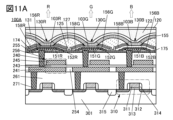
- the substrate 301 corresponds to the substrate 291 in FIG. 10A and FIG. 10B.
- the transistor 310 is a transistor having a channel formation region in the substrate 301.
- a semiconductor substrate such as a single crystal silicon substrate can be used as the substrate 301.
- the transistor 310 has a part of the substrate 301, a conductive layer 311, a low resistance region 312, an insulating layer 313, and an insulating layer 314.
- the conductive layer 311 functions as a gate electrode.
- the insulating layer 313 is located between the substrate 301 and the conductive layer 311 and functions as a gate insulating layer.
- the low resistance region 312 is a region in which the substrate 301 is doped with impurities, and functions as a source or drain.
- the insulating layer 314 is provided to cover the side surface of the conductive layer 311.
- an insulating layer 261 is provided covering the transistor 310, and a capacitor 240 is provided on the insulating layer 261.
- the conductive layer 241 is provided on the insulating layer 261 and is embedded in the insulating layer 254.
- the conductive layer 241 is electrically connected to one of the source and drain of the transistor 310 by a plug 271 embedded in the insulating layer 261.
- the insulating layer 243 is provided to cover the conductive layer 241.
- the conductive layer 245 is provided in a region that overlaps with the conductive layer 241 via the insulating layer 243.
- An insulating layer 255 is provided covering the capacitor 240, an insulating layer 174 is provided on the insulating layer 255, and an insulating layer 175 is provided on the insulating layer 174.
- Light-emitting device 130R, light-emitting device 130G, and light-emitting device 130B are provided on the insulating layer 175.
- An insulator is provided in the area between adjacent light-emitting devices.
- Insulating layer 156R is provided so as to have an area overlapping with the side of conductive layer 151R, insulating layer 156G is provided so as to have an area overlapping with the side of conductive layer 151G, and insulating layer 156B is provided so as to have an area overlapping with the side of conductive layer 151B.
- Conductive layer 152R is provided so as to cover conductive layer 151R and insulating layer 156R, conductive layer 152G is provided so as to cover conductive layer 151G and insulating layer 156G, and conductive layer 152B is provided so as to cover conductive layer 151B and insulating layer 156B.
- Sacrificial layer 158R is located on first layer 135R, sacrificial layer 158G is located on first layer 135G, and sacrificial layer 158B is located on first layer 135B.
- the conductive layer 151R, the conductive layer 151G, and the conductive layer 151B are electrically connected to one of the source or drain of the transistor 310 by the insulating layer 243, the insulating layer 255, the insulating layer 174, the plug 256 embedded in the insulating layer 175, the conductive layer 241 embedded in the insulating layer 254, and the plug 271 embedded in the insulating layer 261.
- Various conductive materials can be used for the plug.
- a protective layer 131 is provided on the light-emitting devices 130R, 130G, and 130B.
- the substrate 120 is attached to the protective layer 131 by a resin layer 122.
- the substrate 120 corresponds to the substrate 292 in FIG. 10A.
- FIG. 11B is a modified example of the display device 100A shown in FIG. 11A.
- the display device shown in FIG. 11B has a colored layer 132R, a colored layer 132G, and a colored layer 132B, and the light-emitting device 130 has an area where it overlaps with one of the colored layers 132R, 132G, and 132B.
- the light-emitting device 130 can emit, for example, white light.
- the colored layer 132R can transmit red light
- the colored layer 132G can transmit green light
- the colored layer 132B can transmit blue light.
- Display device 100B has a configuration in which substrate 352 and substrate 351 are bonded together.
- substrate 352 is indicated by a dashed line.
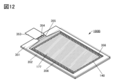
- the display device 100B has a pixel portion 177, a connection portion 140, a circuit 356, wiring 355, and the like.
- FIG. 12 shows an example in which an IC 354 and an FPC 353 are mounted on the display device 100B. Therefore, the configuration shown in FIG. 12 can also be called a display module having the display device 100B, an IC (integrated circuit), and an FPC.
- a display device with a connector such as an FPC attached to the substrate, or a display device with an IC mounted on the substrate, is called a display module.
- a scanning line driver circuit can be used as the circuit 356.
- an example is shown in which an IC 354 is provided on a substrate 351 by a chip on glass (COG) method or a chip on film (COF) method.
- COG chip on glass
- COF chip on film
- an IC having a scanning line driver circuit or a signal line driver circuit can be used as the IC 354.
- the display device 100B and the display module may be configured without an IC.
- the IC may be mounted on an FPC by a COF method, for example.
- Figure 13 shows an example of a cross section of the display device 100B when a portion of the region including the FPC 353, a portion of the circuit 356, a portion of the pixel portion 177, a portion of the connection portion 140, and a portion of the region including the end portion are cut away.
- light-emitting device 130R for details of light-emitting device 130R, light-emitting device 130G, and light-emitting device 130B, please refer to embodiment 1.
- Conductive layers 224R, 224G, and 224B have recesses formed therein to cover the openings provided in insulating layer 214. Layer 128 is embedded in the recesses.
- a protective layer 131 is provided on the light-emitting device 130R, the light-emitting device 130G, and the light-emitting device 130B.
- the protective layer 131 and the substrate 352 are bonded via an adhesive layer 142.
- the substrate 352 is provided with a light-shielding layer 157.
- a solid sealing structure, a hollow sealing structure, or the like can be applied to seal the light-emitting device 130.
- the space between the substrate 352 and the substrate 351 is filled with the adhesive layer 142, and a solid sealing structure is applied.
- the space may be filled with an inert gas (nitrogen, argon, etc.) and a hollow sealing structure may be applied.
- the adhesive layer 142 may be provided so as not to overlap with the light-emitting device.
- the space may also be filled with a resin different from the adhesive layer 142 provided in a frame shape.
- connection portion 140 has a conductive layer 224C obtained by processing the same conductive film as the conductive layers 224R, 224G, and 224B, a conductive layer 151C obtained by processing the same conductive film as the conductive layers 151R, 151G, and 151B, and a conductive layer 152C obtained by processing the same conductive film as the conductive layers 152R, 152G, and 152B.
- FIG. 13 shows an example in which an insulating layer 156C is provided so as to have an area overlapping with the side of the conductive layer 151C.
- the display device 100B is a top emission type. Light emitted by the light emitting device is emitted to the substrate 352 side.
- the substrate 352 is preferably made of a material that is highly transparent to visible light.
- the light emitting element emits infrared or near infrared light, it is preferably made of a material that is highly transparent to the infrared light.
- the first electrode (pixel electrode) contains a material that reflects visible light
- the counter electrode (second electrode 102) contains a material that transmits visible light.
- an insulating layer 211, an insulating layer 213, an insulating layer 215, and an insulating layer 214 are provided in this order.
- a part of the insulating layer 211 functions as a gate insulating layer for each transistor.
- a part of the insulating layer 213 functions as a gate insulating layer for each transistor.
- the insulating layer 215 is provided to cover the transistor.
- the insulating layer 214 is provided to cover the transistor and functions as a planarizing layer. Note that the number of gate insulating layers and the number of insulating layers covering the transistors are not limited, and each may be a single layer or two or more layers.
- An organic insulating layer is suitable for the insulating layer 214, which functions as a planarizing layer.
- Transistor 201 and transistor 205 have a conductive layer 221 that functions as a gate, an insulating layer 211 that functions as a gate insulating layer, conductive layers 222a and 222b that function as a source and a drain, a semiconductor layer 231, an insulating layer 213 that functions as a gate insulating layer, and a conductive layer 223 that functions as a gate.
- a connection portion 204 is provided in an area of the substrate 351 where the substrate 352 does not overlap.
- the wiring 355 is electrically connected to the FPC 353 via the conductive layer 166 and the connection layer 242.
- the conductive layer 166 is an example of a laminated structure of a conductive film obtained by processing the same conductive film as the conductive layers 224R, 224G, and 224B, a conductive film obtained by processing the same conductive film as the conductive layers 151R, 151G, and 151B, and a conductive film obtained by processing the same conductive film as the conductive layers 152R, 152G, and 152B.
- the conductive layer 166 is exposed on the upper surface of the connection portion 204. This allows the connection portion 204 and the FPC 353 to be electrically connected via the connection layer 242.
- the light-shielding layer 157 can be provided between adjacent light-emitting devices, on the connection portion 140, on the circuit 356, and the like.
- various optical components can be disposed on the outside of the substrate 352.
- Substrate 351 and substrate 352 can each be made of a material that can be used for substrate 120.
- the adhesive layer 142 can be made of a material that can be used for the resin layer 122.
- connection layer 242 may be an anisotropic conductive film (ACF) or an anisotropic conductive paste (ACP), etc.
- ACF anisotropic conductive film
- ACP anisotropic conductive paste
- a display device 100D shown in FIG. 14 differs from the display device 100A shown in FIG. 13 mainly in that it is a bottom-emission type display device.
- Light emitted by the light-emitting device is emitted toward the substrate 351. It is preferable to use a material that is highly transparent to visible light for the substrate 351. On the other hand, the translucency of the material used for the substrate 352 does not matter.
- FIG. 14 shows an example in which the light-shielding layer 1117 is provided on the substrate 351, the insulating layer 153 is provided on the light-shielding layer 1117, and the transistors 201, 205, etc. are provided on the insulating layer 153.
- the conductive layers 112R, 112B, 126R, 126B, 129R, and 129B are each made of a material that is highly transparent to visible light. It is preferable to use a material that reflects visible light for the second electrode 102.
- the light-emitting device 130G is not shown in FIG. 14, the light-emitting device 130G is also provided.
- Display device 100E The display device 100E shown in FIG. 15 is a modification of the display device 100B shown in FIG. 13, and differs from the display device 100B mainly in that it has colored layers 132R, 132G, and 132B.
- the light-emitting device 130 has an area that overlaps one of the colored layers 132R, 132G, and 132B.
- the colored layers 132R, 132G, and 132B can be provided on the surface of the substrate 352 facing the substrate 351.
- the ends of the colored layers 132R, 132G, and 132B can overlap the light-shielding layer 157.
- the light-emitting device 130 can emit, for example, white light.
- the colored layer 132R can transmit red light
- the colored layer 132G can transmit green light
- the colored layer 132B can transmit blue light.
- the display device 100E may be configured such that the colored layers 132R, 132G, and 132B are provided between the protective layer 131 and the adhesive layer 142.
- Figures 13 and 15 show an example in which the top surface of layer 128 has a flat portion, but the shape of layer 128 is not particularly limited.
- the electronic device of this embodiment has a display device of one embodiment of the present invention in a display portion.
- the display device of one embodiment of the present invention has high display performance and can easily achieve high definition and high resolution. Therefore, the display device can be used in the display portion of various electronic devices.
- Examples of electronic devices include television devices, desktop or notebook personal computers, computer monitors, digital signage, large game machines such as pachinko machines, and other electronic devices with relatively large screens, as well as digital cameras, digital video cameras, digital photo frames, mobile phones, portable game machines, personal digital assistants, and audio playback devices.
- the display device of one embodiment of the present invention can be used favorably in electronic devices having a relatively small display unit, since it is possible to increase the resolution.
- electronic devices include wristwatch-type and bracelet-type information terminals (wearable devices), as well as wearable devices that can be worn on the head, such as VR devices such as head-mounted displays, glasses-type AR devices, and MR devices.
- the electronic device of this embodiment may have a sensor (including a function to measure force, displacement, position, speed, acceleration, angular velocity, rotation speed, distance, light, liquid, magnetism, temperature, chemicals, sound, time, hardness, electric field, current, voltage, power, radiation, flow rate, humidity, gradient, vibration, odor, or infrared light).
- a sensor including a function to measure force, displacement, position, speed, acceleration, angular velocity, rotation speed, distance, light, liquid, magnetism, temperature, chemicals, sound, time, hardness, electric field, current, voltage, power, radiation, flow rate, humidity, gradient, vibration, odor, or infrared light).
- a display device can be applied to the display panel 751. Therefore, the electronic device can be highly reliable.
- Electronic device 700A and electronic device 700B may be provided with a camera capable of capturing an image of the front as an imaging unit. Furthermore, electronic device 700A and electronic device 700B may each be provided with an acceleration sensor such as a gyro sensor, thereby detecting the orientation of the user's head and displaying an image corresponding to that orientation in display area 756.
- an acceleration sensor such as a gyro sensor
- the housing 721 may be provided with a touch sensor module.
- the display unit 820 is provided inside the housing 821 at a position that can be seen through the lens 832. In addition, by displaying different images on the pair of display units 820, it is also possible to perform three-dimensional display using parallax.
- electronic device 800A and electronic device 800B each have a mechanism that allows the left-right positions of lens 832 and display unit 820 to be adjusted so that they are optimally positioned according to the position of the user's eyes.
- the attachment section 823 allows the user to attach the electronic device 800A or electronic device 800B to the head.
- Each of the electronic devices 800A and 800B may have an input terminal.
- the input terminal can be connected to a cable that supplies a video signal from a video output device or the like, and power for charging a battery provided within the electronic device.
- the electronic device of one embodiment of the present invention may have a function of wireless communication with the earphone 750.
- the electronic device 800B shown in FIG. 16D has an earphone unit 827.
- the earphone unit 827 and the control unit 824 can be configured to be connected to each other by wire.
- both glasses-type devices such as electronic device 700A and electronic device 700B
- goggle-type devices such as electronic device 800A and electronic device 800B
- a display device can be applied to the display portion 6502. Therefore, the electronic device can be highly reliable.
- Figure 17B is a schematic cross-sectional view including the end of the housing 6501 on the microphone 6506 side.
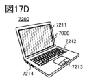
- a display device can be applied to the display portion 7000. Therefore, the electronic device can be highly reliable.
- PCBBiF N-(biphenyl-4-yl)-N-[4-(9-phenyl-9H-carbazol-3-yl)phenyl]-9,9-dimethyl-9H-fluoren-2-amine
- PCBBiF N-(biphenyl-4-yl)-N-[4-(9-phenyl-9H-carbazol-3-yl)phenyl]-9,9-dimethyl-9H-fluoren-2-amine
- OCHD-003 electron acceptor material
- the substrate was left to stand for 1 hour in an air atmosphere while shielded from light, and then heat-treated at 110° C. for 1 hour in an atmosphere of about 1 ⁇ 10 ⁇ 4 Pa or less.
- the light-emitting device was sealed with a glass substrate to prevent it from being exposed to the atmosphere (a UV-curable sealant was applied around the element, UV was irradiated only onto the sealant without irradiating the light-emitting device, and heat treatment was performed at 80°C under atmospheric pressure for 1 hour), producing light-emitting device 1-1.
- the light-emitting device 1-2 was fabricated in the same manner as the light-emitting device 1-1, except that after forming the electron transport layer, the light-emitting device 1-2 was left standing in an air atmosphere under irradiation with a fluorescent lamp.
- the illuminance of the fluorescent lamp was 317 lux.
- Light-emitting device 2-1 was prepared in the same manner as light-emitting device 1-1, except that BP-Icz(II)Tzn in light-emitting device 1-1 was changed to 9-[3-(4,6-diphenyl-1,3,5-triazin-2-yl)phenyl]-9′-phenyl-2,3′-bi-9H-carbazole (abbreviation: mPCCzPTzn-02) represented by the above structural formula (viii).
- the light-emitting device 2-2 was fabricated in the same manner as the light-emitting device 2-1, except that after forming the electron transport layer, the light-emitting device 2-2 was left standing in an air atmosphere under irradiation with a fluorescent lamp.
- the illuminance of the fluorescent lamp was 317 lux.
- Light-emitting device 3-1 was prepared in the same manner as light-emitting device 1-1, except that BP-Icz(II)Tzn in light-emitting device 1-1 was changed to 4- ⁇ 4-[2-(N-phenyl-9H-carbazol-3-yl)-9H-carbazol-9-yl]phenyl ⁇ benzofuro[3,2-d]pyrimidine (abbreviation: 4PCCzPBfpm) represented by the above structural formula (ix).
- the light-emitting device 3-2 was fabricated in the same manner as the light-emitting device 3-1, except that after forming the electron transport layer, the light-emitting device 3-2 was left standing in an air atmosphere under irradiation with a fluorescent lamp.
- the illuminance of the fluorescent lamp was 317 lux.
- Light-emitting device 4-1 was prepared in the same manner as light-emitting device 1-1, except that BP-Icz(II)Tzn in light-emitting device 1-1 was replaced with 4,6-bis[3-(dibenzothiophen-4-yl)phenyl]pyrimidine (abbreviation: 4,6mDBTP2Pm-II) represented by the above structural formula (x).
- 4,6mDBTP2Pm-II 4,6mDBTP2Pm-II
- the light-emitting device 4-2 was fabricated in the same manner as the light-emitting device 4-1, except that after forming the electron transport layer, the light-emitting device 4-2 was left standing in an air atmosphere in an environment irradiated with a fluorescent lamp.
- the illuminance of the fluorescent lamp was 317 lux.
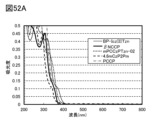
- Figures 19 to 22 show the absorption spectra of the organic compounds used in the light-emitting layers of light-emitting devices 1 to 4, as well as the emission spectra of a fluorescent lamp and orange light, respectively.
- the absorption spectrum of the host material was measured in a thin film state. Specifically, each organic compound was formed into a thin film with a thickness of approximately 50 nm on a quartz substrate and then measured. A UV-visible spectrophotometer (U-4100, manufactured by Hitachi, Ltd.) was used for the measurements. The absorption spectrum of the thin film was calculated from the absorbance (-log10(%T/(100-%R))) calculated from the transmittance (%T) and reflectance (%R) including the substrate.
- each of the substances (host material and assist material) other than the light-emitting substance used in light-emitting device 1 to light-emitting device 4 satisfies any one of the following: the wavelength of the absorption edge located at the longest wavelength in the absorption spectrum is less than 400 nm, the structure does not include any of a structure in which two adjacent six-membered aromatic rings are condensed, a structure in which two adjacent six-membered heteroaromatic rings are condensed, and a structure in which an adjacent six-membered aromatic ring and a six-membered heteroaromatic ring are condensed, the condensed rings are condensed rings in which six-membered rings and five-membered rings are condensed alternately, or the condensed rings do not include a naphthalene skeleton, do not include any of a naphthalene ring, a phenanthrene ring, and a naphthacen
- the absorption edge located at the longest wavelength among the absorption edges of the absorption spectrum was 372 nm for ⁇ NCCP, 398 nm for BP-Icz(II)Tzn, 375 nm for mPCCzPTzn-02, 448 nm for 4PCCzPBfpm, and 355 nm for 4,6mDBTP2Pm-II.
- the absorbance of ⁇ NCCP, BP-Icz(II)Tzn, and mPCCzPTzn-02 at wavelengths of 400 nm or more and 475 nm or less was 0.01 or less.
- FIG 27 shows the results of measuring the change in luminance with respect to drive time during constant current drive at a current density of 50 mA/ cm2 .
- no difference was observed in the change in luminance with respect to drive time regardless of whether or not the device was irradiated with a fluorescent lamp.
- Light-emitting device 5 A manufacturing method and characteristics of the light-emitting device 5, which is a light-emitting device that exhibits blue phosphorescence and is one embodiment of the present invention, are described in detail below. Organic compounds used in the light-emitting device 5 are described below.
- Method of Manufacturing Light-Emitting Device 5-1 First, on a glass substrate, 100 nm of silver (Ag) was laminated as a reflective electrode from the substrate side, followed by 85 nm of indium tin oxide containing silicon oxide (ITSO) as a transparent electrode, by sputtering to form a first electrode 101 having a size of 2 mm x 2 mm.
- the ITSO functions as an anode, and is regarded as the first electrode 101 together with the laminated structure of Ag.
- the substrate surface was washed with water as a pretreatment for forming a light-emitting device on the substrate.
- the substrate was introduced into a vacuum deposition apparatus whose inside had been reduced in pressure to about 1 ⁇ 10 ⁇ 4 Pa, and vacuum baking was carried out at 170° C. for 30 minutes in a heating chamber in the vacuum deposition apparatus, and then the substrate was allowed to cool for about 30 minutes.
- BBABnf N,N-bis(4-biphenyl)-6-phenylbenzo[b]naphtho[1,2-d]furan-8-amine
- xi structural formula
- OCHD-003 electron acceptor material
- PCCP 3,3'-bis(9-phenyl-9H-carbazole) represented by the above structural formula (xii) was deposited to a thickness of 20 nm to form the hole transport layer 112.
- DBT3P-II 4,4',4''-(benzene-1,3,5-triyl)tri(dibenzothiophene) represented by the above structural formula (v) was formed on the second electrode 102 as a cap layer to improve the light extraction efficiency.
- the light-emitting device was sealed with a glass substrate to prevent it from being exposed to the atmosphere (a UV-curable sealant was applied around the element, UV was irradiated only onto the sealant without irradiating the light-emitting device, and heat treatment was performed at 80°C under atmospheric pressure for 1 hour), to produce light-emitting device 5-1.
- the light-emitting device 5-2 was fabricated in the same manner as the light-emitting device 5-1, except that after forming the electron transport layer, the light-emitting device 5-2 was left standing in an air atmosphere in an environment irradiated with a fluorescent lamp.
- the illuminance of the fluorescent lamp was 317 lux.
- Light-emitting device 5-3 was fabricated in the same manner as light-emitting device 5-1, except that after forming the electron transport layer in light-emitting device 5-1, the device was left standing in an air atmosphere under irradiation with orange light. The illuminance of the orange light was 111 lux.
- Comparative Light-Emitting Device 1 Comparative Light-Emitting Device 2
- the following provides a detailed description of the manufacturing method and characteristics of comparative light-emitting devices 1 and 2, which are light-emitting devices for comparison that emit blue fluorescence.
- the organic compounds used in the comparative light-emitting devices 1 and 2 are shown below.
- the substance (host material) other than the light-emitting substance used in comparative light-emitting device 1 is not a light-emitting device according to one embodiment of the present invention, because the absorption edge wavelength located at the longest wavelength in its absorption spectrum is 400 nm or more, it has a structure in which two adjacent six-membered aromatic rings are condensed, it contains a naphthalene skeleton, and it contains a fused ring composed only of six-membered rings.
- the luminance-current density characteristics of these comparative light-emitting devices 1 are shown in Fig. 37, the current efficiency-luminance characteristics in Fig. 38, the luminance-voltage characteristics in Fig. 39, the current density-voltage characteristics in Fig. 40, the blue index-luminance characteristics in Fig. 41, and the emission spectrum in Fig. 42.
- the main values of voltage, current, current density, CIE chromaticity, current efficiency, and blue index at around 1000 cd/ cm2 are shown below.
- the luminance, CIE chromaticity, and emission spectrum were measured at room temperature using a spectroradiometer (SR-UL1R, manufactured by Topcon Corporation).
Landscapes
- Engineering & Computer Science (AREA)
- Chemical & Material Sciences (AREA)
- Physics & Mathematics (AREA)
- Materials Engineering (AREA)
- Spectroscopy & Molecular Physics (AREA)
- Optics & Photonics (AREA)
- Inorganic Chemistry (AREA)
- General Physics & Mathematics (AREA)
- Theoretical Computer Science (AREA)
- Microelectronics & Electronic Packaging (AREA)
- Crystallography & Structural Chemistry (AREA)
- Manufacturing & Machinery (AREA)
- Electroluminescent Light Sources (AREA)
Priority Applications (4)
| Application Number | Priority Date | Filing Date | Title |
|---|---|---|---|
| JP2024566911A JPWO2024141880A1 (https=) | 2022-12-28 | 2023-12-21 | |
| KR1020257022207A KR20250129675A (ko) | 2022-12-28 | 2023-12-21 | 발광 디바이스 |
| DE112023005443.6T DE112023005443T5 (de) | 2022-12-28 | 2023-12-21 | Licht emittierende Vorrichtung |
| CN202380089161.XA CN120419333A (zh) | 2022-12-28 | 2023-12-21 | 发光器件 |
Applications Claiming Priority (2)
| Application Number | Priority Date | Filing Date | Title |
|---|---|---|---|
| JP2022-212557 | 2022-12-28 | ||
| JP2022212557 | 2022-12-28 |
Publications (1)
| Publication Number | Publication Date |
|---|---|
| WO2024141880A1 true WO2024141880A1 (ja) | 2024-07-04 |
Family
ID=91716602
Family Applications (1)
| Application Number | Title | Priority Date | Filing Date |
|---|---|---|---|
| PCT/IB2023/063058 Ceased WO2024141880A1 (ja) | 2022-12-28 | 2023-12-21 | 発光デバイス |
Country Status (5)
| Country | Link |
|---|---|
| JP (1) | JPWO2024141880A1 (https=) |
| KR (1) | KR20250129675A (https=) |
| CN (1) | CN120419333A (https=) |
| DE (1) | DE112023005443T5 (https=) |
| WO (1) | WO2024141880A1 (https=) |
Citations (2)
| Publication number | Priority date | Publication date | Assignee | Title |
|---|---|---|---|---|
| JP2017108108A (ja) * | 2015-09-30 | 2017-06-15 | 株式会社半導体エネルギー研究所 | 発光素子、表示装置、電子機器、及び照明装置 |
| WO2022123383A1 (ja) * | 2020-12-07 | 2022-06-16 | 株式会社半導体エネルギー研究所 | 表示装置の作製方法 |
Family Cites Families (1)
| Publication number | Priority date | Publication date | Assignee | Title |
|---|---|---|---|---|
| US10862036B2 (en) | 2015-06-29 | 2020-12-08 | Imec Vzw | Method for high resolution patterning of organic layers |
-
2023
- 2023-12-21 WO PCT/IB2023/063058 patent/WO2024141880A1/ja not_active Ceased
- 2023-12-21 KR KR1020257022207A patent/KR20250129675A/ko active Pending
- 2023-12-21 DE DE112023005443.6T patent/DE112023005443T5/de active Pending
- 2023-12-21 CN CN202380089161.XA patent/CN120419333A/zh active Pending
- 2023-12-21 JP JP2024566911A patent/JPWO2024141880A1/ja active Pending
Patent Citations (2)
| Publication number | Priority date | Publication date | Assignee | Title |
|---|---|---|---|---|
| JP2017108108A (ja) * | 2015-09-30 | 2017-06-15 | 株式会社半導体エネルギー研究所 | 発光素子、表示装置、電子機器、及び照明装置 |
| WO2022123383A1 (ja) * | 2020-12-07 | 2022-06-16 | 株式会社半導体エネルギー研究所 | 表示装置の作製方法 |
Also Published As
| Publication number | Publication date |
|---|---|
| CN120419333A (zh) | 2025-08-01 |
| KR20250129675A (ko) | 2025-08-29 |
| DE112023005443T5 (de) | 2025-10-16 |
| JPWO2024141880A1 (https=) | 2024-07-04 |
Similar Documents
| Publication | Publication Date | Title |
|---|---|---|
| JP2024079628A (ja) | 発光デバイス | |
| KR20250065821A (ko) | 발광 디바이스 및 표시 장치 | |
| WO2024141880A1 (ja) | 発光デバイス | |
| JP2025031662A (ja) | 表示装置 | |
| JP2025105556A (ja) | 発光デバイスおよび表示装置 | |
| WO2024241140A1 (ja) | 有機半導体デバイスの作製方法、発光デバイスの作製方法、およびフォトセンサの作製方法 | |
| WO2024218626A1 (ja) | 発光デバイス | |
| JP2025105563A (ja) | 発光デバイスおよび表示装置 | |
| WO2023209492A1 (ja) | 発光デバイスおよび発光装置の作製方法 | |
| JP2024167068A (ja) | 発光デバイス、発光装置、電子機器 | |
| KR20250114508A (ko) | 발광 디바이스 | |
| WO2025104569A1 (ja) | 発光デバイスの作製方法 | |
| WO2025196605A1 (ja) | 発光デバイスおよび表示装置 | |
| JP2024079655A (ja) | 発光デバイス | |
| KR20250172393A (ko) | 발광 디바이스 | |
| WO2025186690A1 (ja) | 発光デバイスおよび表示装置 | |
| WO2025032476A1 (ja) | 有機半導体デバイス、発光デバイス、受光デバイスおよび表示装置 | |
| KR20260020938A (ko) | 표시 장치 | |
| WO2025078925A1 (ja) | 発光デバイスおよび発光装置 | |
| JP2025088765A (ja) | 発光装置用材料および発光デバイス | |
| WO2023187545A1 (ja) | 発光デバイスの作製方法 | |
| JP2024079659A (ja) | 発光デバイス | |
| JP2024146902A (ja) | 発光デバイス | |
| KR20250157967A (ko) | 발광 디바이스 및 표시 장치 | |
| KR20250177346A (ko) | 발광 디바이스 및 표시 장치 |
Legal Events
| Date | Code | Title | Description |
|---|---|---|---|
| 121 | Ep: the epo has been informed by wipo that ep was designated in this application |
Ref document number: 23911078 Country of ref document: EP Kind code of ref document: A1 |
|
| WWE | Wipo information: entry into national phase |
Ref document number: 2024566911 Country of ref document: JP |
|
| WWE | Wipo information: entry into national phase |
Ref document number: 202380089161.X Country of ref document: CN |
|
| WWE | Wipo information: entry into national phase |
Ref document number: 1020257022207 Country of ref document: KR |
|
| WWE | Wipo information: entry into national phase |
Ref document number: 112023005443 Country of ref document: DE |
|
| WWP | Wipo information: published in national office |
Ref document number: 202380089161.X Country of ref document: CN |
|
| WWP | Wipo information: published in national office |
Ref document number: 1020257022207 Country of ref document: KR |
|
| WWP | Wipo information: published in national office |
Ref document number: 112023005443 Country of ref document: DE |
|
| 122 | Ep: pct application non-entry in european phase |
Ref document number: 23911078 Country of ref document: EP Kind code of ref document: A1 |