WO2024135286A1 - 半導体記憶装置およびトランジスタ装置 - Google Patents
半導体記憶装置およびトランジスタ装置 Download PDFInfo
- Publication number
- WO2024135286A1 WO2024135286A1 PCT/JP2023/043035 JP2023043035W WO2024135286A1 WO 2024135286 A1 WO2024135286 A1 WO 2024135286A1 JP 2023043035 W JP2023043035 W JP 2023043035W WO 2024135286 A1 WO2024135286 A1 WO 2024135286A1
- Authority
- WO
- WIPO (PCT)
- Prior art keywords
- layer
- memory device
- semiconductor memory
- conductive pillar
- wiring
- Prior art date
- Legal status (The legal status is an assumption and is not a legal conclusion. Google has not performed a legal analysis and makes no representation as to the accuracy of the status listed.)
- Ceased
Links
Images

Classifications
-
- H—ELECTRICITY
- H10—SEMICONDUCTOR DEVICES; ELECTRIC SOLID-STATE DEVICES NOT OTHERWISE PROVIDED FOR
- H10B—ELECTRONIC MEMORY DEVICES
- H10B53/00—Ferroelectric RAM [FeRAM] devices comprising ferroelectric memory capacitors
- H10B53/30—Ferroelectric RAM [FeRAM] devices comprising ferroelectric memory capacitors characterised by the memory core region
-
- H—ELECTRICITY
- H10—SEMICONDUCTOR DEVICES; ELECTRIC SOLID-STATE DEVICES NOT OTHERWISE PROVIDED FOR
- H10D—INORGANIC ELECTRIC SEMICONDUCTOR DEVICES
- H10D64/00—Electrodes of devices having potential barriers
- H10D64/01—Manufacture or treatment
- H10D64/011—Manufacture or treatment of electrodes ohmically coupled to a semiconductor
-
- H—ELECTRICITY
- H10—SEMICONDUCTOR DEVICES; ELECTRIC SOLID-STATE DEVICES NOT OTHERWISE PROVIDED FOR
- H10P—GENERIC PROCESSES OR APPARATUS FOR THE MANUFACTURE OR TREATMENT OF DEVICES COVERED BY CLASS H10
- H10P14/00—Formation of materials, e.g. in the shape of layers or pillars
- H10P14/40—Formation of materials, e.g. in the shape of layers or pillars of conductive or resistive materials
-
- H—ELECTRICITY
- H10—SEMICONDUCTOR DEVICES; ELECTRIC SOLID-STATE DEVICES NOT OTHERWISE PROVIDED FOR
- H10W—GENERIC PACKAGES, INTERCONNECTIONS, CONNECTORS OR OTHER CONSTRUCTIONAL DETAILS OF DEVICES COVERED BY CLASS H10
- H10W20/00—Interconnections in chips, wafers or substrates
- H10W20/01—Manufacture or treatment
-
- H—ELECTRICITY
- H10—SEMICONDUCTOR DEVICES; ELECTRIC SOLID-STATE DEVICES NOT OTHERWISE PROVIDED FOR
- H10W—GENERIC PACKAGES, INTERCONNECTIONS, CONNECTORS OR OTHER CONSTRUCTIONAL DETAILS OF DEVICES COVERED BY CLASS H10
- H10W20/00—Interconnections in chips, wafers or substrates
- H10W20/40—Interconnections external to wafers or substrates, e.g. back-end-of-line [BEOL] metallisations or vias connecting to gate electrodes
- H10W20/45—Interconnections external to wafers or substrates, e.g. back-end-of-line [BEOL] metallisations or vias connecting to gate electrodes characterised by their insulating parts
- H10W20/48—Insulating materials thereof
Definitions
- This disclosure relates to semiconductor memory devices and transistor devices.
- CMOS circuits are used in many LSI (Large Scale Integration) devices.
- LSI devices have been commercialized as SoCs (System on a Chip), which combine analog circuits, memory, and logic circuits on a single chip.
- SRAM static random access memory
- DRAM dynamic RAM
- MRAM magnetic RAM
- FeRAM ferroelectric RAM
- Patent Document 1 A semiconductor memory device that functions as an FeRAM using such a ferroelectric capacitor has already been proposed (for example, Patent Document 1).
- a semiconductor memory device comprises a semiconductor substrate including a thin-film transistor, first and second wirings stacked on the semiconductor substrate, a contact section including a first conductive pillar extending in the stacking direction of the semiconductor substrate and the first and second wirings and electrically connecting the thin-film transistor to the first wiring, and a capacitor section including a second conductive pillar extending in the stacking direction and electrically connecting the thin-film transistor to the second wiring.
- the height position of the top end of the first conductive pillar on the side opposite the semiconductor substrate and the height position of the top end of the second conductive pillar on the side opposite the semiconductor substrate are substantially the same.
- the semiconductor memory device has a structure that is suitable for miniaturization and can be easily manufactured.
- FIG. 1 is a circuit diagram showing an example of an equivalent circuit of a semiconductor memory device according to a first embodiment of the present disclosure.
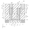
- FIG. 2 is a schematic diagram showing an example of a cross-sectional configuration along the stacking direction of the semiconductor memory device shown in FIG.
- FIG. 3 is a schematic diagram showing an example of a planar configuration of the semiconductor memory device shown in FIG.
- FIG. 4 is a schematic diagram showing an example of a cross-sectional configuration along an in-plane direction of the semiconductor memory device shown in FIG.
- FIG. 5A is a schematic diagram illustrating one step of a method for manufacturing the semiconductor memory device shown in FIG.
- FIG. 5B is a schematic diagram illustrating a step following FIG. 5A.
- FIG. 5C is a schematic diagram illustrating a step following FIG.
- FIG. 5D is a schematic diagram illustrating a step following FIG. 5C.
- FIG. 5E is a schematic diagram illustrating a step following FIG. 5D.
- FIG. 5F is a schematic diagram illustrating a step following FIG. 5E.
- FIG. 5G is a schematic diagram illustrating a step following FIG. 5F.
- FIG. 5H is a schematic diagram illustrating a step following FIG. 5G.
- FIG. 6 is a schematic diagram showing an example of a cross-sectional configuration along the stacking direction of a semiconductor memory device according to a first modified example of the first embodiment of the present disclosure.
- FIG. 6 is a schematic diagram showing an example of a cross-sectional configuration along the stacking direction of a semiconductor memory device according to a first modified example of the first embodiment of the present disclosure.
- FIG. 7 is a schematic diagram showing an example of a cross-sectional configuration along the stacking direction of a semiconductor memory device according to a second modification of the first embodiment of the present disclosure.
- FIG. 8 is a schematic diagram showing an example of a cross-sectional configuration along the stacking direction of a semiconductor memory device according to a third modified example of the first embodiment of the present disclosure.
- FIG. 9 is a schematic diagram showing an example of a cross-sectional configuration along the stacking direction of a semiconductor memory device according to a fourth modified example of the first embodiment of the present disclosure.
- FIG. 10 is a schematic diagram showing an example of a cross-sectional configuration along the stacking direction of a semiconductor memory device according to a fifth modified example of the first embodiment of the present disclosure.
- FIG. 11 is a schematic diagram showing an example of a cross-sectional configuration along the stacking direction of a semiconductor memory device according to a sixth modified example of the first embodiment of the present disclosure.
- FIG. 12A is a schematic diagram showing an example of a cross-sectional configuration of a transistor device according to a second embodiment of the present disclosure.
- FIG. 12B is another schematic diagram showing an example of the cross-sectional configuration of the transistor device according to the second embodiment of the present disclosure.
- FIG. 13 is a schematic diagram showing an example of a cross-sectional configuration of a transistor device as a reference example.
- FIG. 14 is a schematic diagram showing an example of a cross-sectional configuration along the stacking direction of a semiconductor memory device as a first modified example of the present disclosure.
- FIG. 15 is a schematic diagram showing an example of a cross-sectional configuration along the stacking direction of a semiconductor memory device according to a second modified example of the present disclosure.
- Fig. 1 is a circuit diagram showing an example of an equivalent circuit of the semiconductor memory device 100 according to the present embodiment.
- the semiconductor memory device 100 includes a capacitor C that stores information and a transistor T that controls the selection and non-selection of the capacitor C.
- Capacitor C is a ferroelectric capacitor including a first electrode, a second electrode, and a ferroelectric film sandwiched between the first and second electrodes. Capacitor C can store one bit of information depending on the direction of the remanent polarization of the ferroelectric film. Capacitor C is electrically connected to source line SL at the first electrode, and is electrically connected to the source of transistor T at the second electrode.
- Transistor T is a field effect transistor that controls the application of voltage to capacitor C.
- Transistor T is electrically connected to the other electrode of capacitor C at its source, and is electrically connected to bit line BL at its drain.
- Transistor T is also electrically connected to word line WL at its gate, so that the state of the channel can be controlled by the voltage applied from word line WL.
- a voltage is applied to the word line WL, causing the channel of transistor T to transition to the on state. Then, a potential is applied to each of the source line SL and bit line BL, and an electric field corresponding to the information to be written is applied to the ferroelectric film of capacitor C. This allows the semiconductor memory device 100 to write information to capacitor C by controlling the direction of the remanent polarization of the ferroelectric film of capacitor C with an external electric field.
- the semiconductor memory device 100 when reading information from capacitor C, in the semiconductor memory device 100, first, a voltage is applied to the word line WL, causing the channel of transistor T to transition to the on state. Then, a predetermined potential is applied to each of the source line SL and bit line BL, causing the polarization direction of the ferroelectric film of capacitor C to transition to a predetermined direction. At this time, the magnitude of the current flowing into capacitor C during the transition changes depending on the polarization direction of the ferroelectric film before the transition. Therefore, the semiconductor memory device 100 can read the information stored in capacitor C by measuring the magnitude of the current flowing into capacitor C.
- the semiconductor memory device 100 can operate as a Ferroelectric Random Access Memory (FeRAM) that stores information in a capacitor C that includes a ferroelectric film.
- FeRAM Ferroelectric Random Access Memory
- FIG. 2 shows an example of a cross-sectional configuration along the stacking direction of the semiconductor memory device 100.
- FIG. 3 shows an example of a planar configuration of the semiconductor memory device 100.
- FIG. 4 is an in-plane cross-sectional view of a part of the semiconductor memory device 100 enlarged.
- the insulating films Z1 to Z4 formed spreading over the entire surface of the semiconductor substrate 2 described later are omitted.
- the cross-sectional view of FIG. 2 shows a cross section cut along the line II-II described in FIG. 3.
- the direction along the surface on which the semiconductor substrate 2 extends is referred to as the in-plane direction
- the direction perpendicular to the in-plane direction is referred to as the height direction or stacking direction.
- FIG. 4 one capacitor section 25 (described later) and a part of the second wiring 5 (described later) of the semiconductor memory device 100 are illustrated, and the illustration of other components is omitted.
- the in-plane direction is the XY plane
- the height direction (stacking direction) is the Z-axis direction.
- the semiconductor memory device 100 includes a semiconductor substrate 2, a first wiring 4, a second wiring 5, a contact portion 15, and a capacitor portion 25 serving as a capacitor C.
- the semiconductor substrate 2 is made of a semiconductor material.
- the semiconductor substrate 2 may be a silicon substrate, or may be an SOI (Silicon On Insulator) substrate in which an insulating film such as SiO2 is sandwiched between a silicon substrate.
- the semiconductor substrate 2 may be a substrate made of other semiconductor elements such as germanium, or may be a substrate made of a compound semiconductor such as GaAs (gallium arsenide), GaN (gallium nitride), or SiC (silicon carbide).
- the semiconductor substrate 2 is provided with, for example, a plurality of thin film transistors 1 and an element isolation layer 3.
- the element isolation layer 3 is made of an insulating material and electrically isolates the plurality of thin film transistors 1 provided in the active region of the semiconductor substrate 2 from each other.
- the element isolation layer 3 can be made of an insulating material such as SiOx (silicon oxide), SiNx (silicon nitride), or SiON (silicon oxynitride).
- the element isolation layer 3 can be formed by using the STI (Shallow Trench Isolation) method to remove a portion of the semiconductor substrate 2 in a predetermined region by etching or the like, and then filling the opening formed by etching or the like with SiOx (silicon oxide).
- the element isolation layer 3 can be formed by thermally oxidizing the semiconductor substrate 2 in a predetermined region by using the LOCOS (Local Oxidation of Silicon) method.
- the region isolated from the surroundings by the element isolation layer 3 becomes the active area AA (see FIG. 3) in which the thin-film transistor 1 is provided.
- a first conductivity type impurity for example, a p-type impurity such as boron (B) or aluminum (Al) is introduced.
- the thin-film transistor 1 is, for example, a MOS (Metal Oxide Semiconductor)-FET (Field-Effect Transistor) including a gate electrode 1G, a sidewall insulating film 1W, a gate insulating film 1Z, a drain region 1D, and a source region 1S.
- MOS Metal Oxide Semiconductor
- FET Field-Effect Transistor
- the gate insulating film 1Z is made of an insulating material and is provided on the active area AA of the semiconductor substrate 2.
- the gate insulating film 1Z may be made of an insulating material known as a gate insulating film for a field effect transistor.
- the gate insulating film 1Z may be made of an oxide such as silicon oxide (SiOx).
- the gate electrode 1G is made of a conductive material and is provided on the gate insulating film 1Z. Specifically, the gate electrode 1G extends, for example, in the vertical direction of the paper surface of FIG. 3 (hereinafter referred to as the first direction). The gate electrode 1G extends in the first direction beyond the element isolation layer 3 and is provided so as to straddle multiple active areas AA, thereby forming a word line WL that electrically connects the gates of multiple thin film transistors 1.
- the gate electrode 1G may be formed of, for example, polysilicon, or may be formed of a metal, an alloy, a metal compound, or an alloy of a metal (such as Ni) and polysilicon, i.e., a so-called silicide.
- the gate electrode 1G may be formed of a laminated structure of a metal layer made of TiN or TaN and a polysilicon layer provided on the gate insulating film 1Z. With such a laminated structure, the gate electrode 1G can reduce the wiring resistance compared to when it is formed of only a polysilicon layer.
- the drain region 1D and the source region 1S are second conductivity type regions formed in the semiconductor substrate 2. Specifically, the drain region 1D and the source region 1S are provided to face each other with the gate electrode 1G in between.
- the drain region 1D and the source region 1S are formed, for example, by introducing a second conductivity type impurity (e.g., n-type impurity such as phosphorus (P) or arsenic (As)) into the semiconductor substrate 2 in the active area AA.
- a silicide layer 6 is formed in each of the drain region 1D and the source region 1S on a part of the surface 2FS of the semiconductor substrate 2.
- the drain region 1D is electrically connected to a first wiring 4, e.g., a bit line BL (FIG. 1), via a contact portion 15.
- the source region 1S is electrically connected to a second wiring 5, e.g., a source line SL (FIG. 1), via a capacitor portion 25, e.g., a capacitor C.
- the sidewall insulating film 132 is made of an insulating material and is provided as a sidewall on the side surface of the gate electrode 130.
- the sidewall insulating film 132 can be formed by uniformly depositing an insulating film in a region including the gate electrode 130 and then vertically anisotropically etching the insulating film.
- the sidewall insulating film 132 may be formed in a single layer or multiple layers using an insulating oxynitride such as silicon oxide (SiO x ), silicon nitride (SiN x ), or silicon oxynitride (SiON).
- insulating films Z1 to Z4 are stacked in order on the thin-film transistor 1.
- the insulating films Z1, Z3, and Z4 are, for example, silicon oxide films, and the insulating film Z2 is, for example, a silicon nitride film.
- the contact portion 15 has a first conductive pillar 10, a ferroelectric layer 13, and an electrode layer 14.
- the first conductive pillar 10 is a columnar member having a height H10 that extends in the Z-axis direction so as to penetrate the insulating films Z1 to Z3 from a height position P0 on the surface 2FS of the semiconductor substrate 2 to a height position P10 on the upper surface of the insulating film Z3.
- the first conductive pillar 10 is located between the semiconductor substrate 2 and the first wiring 4 in the Z-axis direction, and electrically connects the thin film transistor 1 to the first wiring 4. As shown in FIGS.
- the first conductive pillar 10 includes, for example, a substantially cylindrical conductive layer 11 and a substantially cylindrical barrier metal layer 12 that surrounds the periphery of the conductive layer 11.
- the conductive layer 11 can be made of a conductive material such as W (tungsten) or polysilicon.
- the barrier metal layer 12 can be made of a metal material such as Ti (titanium), TiN (titanium nitride), or Ru (ruthenium).
- the ferroelectric layer 13 and the electrode layer 14 are provided, for example, at the same level as the insulating film Z3.
- the ferroelectric layer 13 is provided so as to cover the periphery of the barrier metal layer 12.
- the electrode layer 14 is provided so as to cover the periphery of the ferroelectric layer 13.
- the material of the ferroelectric layer 13 is, for example, the same as the material of the ferroelectric layer 23 described later.
- the material of the electrode layer 14 is, for example, the same as the material of the electrode layer 24 described later.
- the ferroelectric layer 13 and the electrode layer 14 do not necessarily have to be present.
- the first wiring 4 is provided at the same layer as the insulating film Z4.
- the first wiring 4 includes, for example, a barrier layer 4A and a buried layer 4B.
- the barrier layer 4A can be composed of, for example, each of Co (cobalt), W (tungsten), Mo (molybdenum), Ru (ruthenium), Ta (tantalum), and Cu (copper), or a compound containing at least one of these elements.
- the buried layer 4B can be made of a conductive material containing Cu (copper) and Ru (ruthenium).
- the capacitor section 25 has a second conductive pillar 20, a ferroelectric layer 23, and an electrode layer 24.
- the ferroelectric layer 23 is sandwiched between the second conductive pillar 20 and the electrode layer 24.
- the second conductive pillar 20 is a columnar member having a height H20 that extends in the Z-axis direction so as to penetrate the insulating films Z1 to Z3 from a height position P0 on the surface 2FS of the semiconductor substrate 2 to a height position P20 on the upper end 20UT.
- the height position P20 coincides with the height position of the upper surface of the insulating film Z3.
- the second conductive pillar 20 electrically connects the thin film transistor 1 and the second wiring 5.
- the second conductive pillar 20 includes, for example, a substantially cylindrical conductive layer 21 and a substantially cylindrical barrier metal layer 22 surrounding the periphery of the conductive layer 21.
- the conductive layer 21 may be made of a conductive material such as W (tungsten) or polysilicon.
- the barrier metal layer 22 may be made of a metal material such as Ti (titanium), TiN (titanium nitride), or Ru (ruthenium).
- the material of the conductive layer 21 may be the same as the material of the conductive layer 11, for example.
- the material of the barrier metal layer 22 may be the same as the material of the barrier metal layer 12, for example.
- the ferroelectric layer 23 and the electrode layer 24 are provided in the same layer as the insulating film Z3, for example.
- the ferroelectric layer 23 is provided so as to cover the periphery of the barrier metal layer 22.
- the electrode layer 24 is provided so as to cover the periphery of the ferroelectric layer 23.
- the ferroelectric layer 23 may be made of a ferroelectric material containing at least one of HfO2 (hafnium oxide), Si (silicon), Zr (zirconium), La (lanthanum), Nb (niobium), Y (yttrium), Ge (germanium), and Sc (scandium).
- the ferroelectric layer 23 may also be made of PZT (lead zirconate titanate), SBT (strontium bismuth tantalate), or BLT.
- the electrode layer 24 may be made of a metal material such as Ti (titanium), TiN (titanium nitride), or Ru (ruthenium).
- the lower end of the second conductive pillar 20 is in contact with the silicide layer 6 provided in the source region 10S.
- a side surface 24S of the electrode layer 24 surrounding the second conductive pillar 20 on the opposite side to the second conductive pillar 20 abuts against a side surface 5S of the second wiring 5.
- the second wiring 5 is provided in the same layer as a part of the insulating film Z3 and a part of the insulating film Z4.
- the second wiring 5 includes, for example, a barrier layer 5A and a buried layer 5B.
- the barrier layer 5A can be composed of, for example, each of Co (cobalt), W (tungsten), Mo (molybdenum), Ru (ruthenium), Ta (tantalum), and Cu (copper), or a compound containing at least one of these elements.
- the buried layer 5B can be made of a conductive material containing Cu (copper) and Ru (ruthenium).
- the constituent material of the barrier layer 5A may be the same as the constituent material of the barrier layer 4A.
- the constituent material of the buried layer 5B can be, for example, the buried layer 4B. 3, the second wiring 5 may be shared by adjacent capacitor sections 25.
- an element isolation layer 3 is formed on a semiconductor substrate 2.
- a SiO 2 film is formed on the semiconductor substrate 2 by dry oxidation or the like, and a Si 3 N 4 film is further formed by low pressure CVD or the like.
- a resist layer patterned to protect the region where the active area AA is to be provided is formed on the Si 3 N 4 film, and then the SiO 2 film, the Si 3 N 4 film, and the semiconductor substrate 2 are etched to a depth of 350 nm to 400 nm.
- SiO 2 is deposited to a thickness of 650 nm to 700 nm, and the openings formed by etching are filled to form the element isolation layer 3.
- high density plasma CVD which has good step coverage and can form a dense SiO 2 film, may be used for the deposition of SiO 2 .
- the excess SiO 2 film is removed by CMP (Chemical Mechanical Polishing) or the like to planarize the surface of the semiconductor substrate 2.
- CMP Chemical Mechanical Polishing
- the SiO 2 film may be removed by CMP until the Si 3 N 4 film is exposed, for example.
- the Si3N4 film is removed using hot phosphoric acid, etc.
- the surface of the region corresponding to the active region AA of the semiconductor substrate 2 is oxidized to a thickness of about 10 nm to form an oxide film, and then a first conductivity type impurity (e.g., boron (B) or the like) is ion-implanted to convert the semiconductor substrate 2 in the active region AA into a first conductivity type well.
- a first conductivity type impurity e.g., boron (B) or the like
- the gate electrode 1G is formed on the gate insulating film 1Z.
- the oxide film covering the surface of the semiconductor substrate 2 is peeled off with a hydrofluoric acid solution or the like.
- a gate insulating film 1Z made of SiO 2 is formed on the semiconductor substrate 2 to a thickness of 1.5 nm to 10 nm by dry oxidation using O 2 or RTA (Rapid Thermal Anneal) processing, for example.
- a gas used for dry oxidation a mixed gas of H 2 /O 2 , N 2 O or NO may be used in addition to O 2.
- polysilicon is deposited to a thickness of 50 nm to 150 nm by low pressure CVD using SiH4 gas as a source gas and a deposition temperature of 580° C. to 620° C. Thereafter, the deposited polysilicon is anisotropically etched using a patterned resist as a mask to form the gate electrode 1G.
- HBr-based gas or Cl-based gas can be used for the anisotropic etching.
- the gate electrodes 11G and 21G may be formed simultaneously and shared with the gate electrodes of other transistors provided in the logic region of the circuit section, etc.
- a drain region 1D and a source region 1S are formed in the active area AA of the semiconductor substrate 2.
- sidewall insulating films 1W are formed on both side surfaces of the gate electrode 1G.
- SiO2 is deposited by plasma CVD to a thickness of 10 nm to 30 nm
- Si3N4 is deposited by plasma CVD to a thickness of 30 nm to 50 nm to form a sidewall insulating film.
- the sidewall insulating film is anisotropically etched to form sidewall insulating films 1W on both side surfaces of the gate electrodes 11G and 21G.
- arsenic (As) which is a second conductive type impurity
- As arsenic
- the ion-implanted impurity is activated by performing RTA (Rapid Thermal Annealing) at 1000° C. for 5 seconds.
- RTA Rapid Thermal Annealing
- the thin film transistor 1 is formed. Note that it is also possible to activate the impurity by spike RTA in order to promote activation of the introduced impurity and suppress diffusion of the impurity.
- an insulating film Z1 is formed over the entire surface of the semiconductor substrate 2 so as to bury the thin film transistor 1.
- SiO 2 is deposited on the semiconductor substrate 2 on which the thin film transistor 1 is formed by using CVD or the like, and then planarized by, for example, CMP to form the insulating film Z1.
- an insulating film Z2 made of, for example, SiN and a sacrificial layer ZG made of SiO 2 are sequentially stacked on the insulating film Z1 by using CVD or the like.
- openings 10K and 20K are formed, each penetrating the laminated film consisting of insulating film Z1, insulating film Z2, and sacrificial layer ZG.
- the silicide layer 6 provided in the drain region 1D is exposed at the bottom of opening 10K.
- the silicide layer 6 provided in the source region 1S is exposed at the bottom of opening 20K.
- a first conductive pillar 10 is formed to fill the inside of the opening 10K
- a second conductive pillar 20 is formed to fill the inside of the opening 20K.
- the height position P10 of the upper end 10UT of the first conductive pillar 10 and the height position P20 of the upper end 20UT of the second conductive pillar 20 coincide with the height position of the upper surface ZGS of the sacrificial layer ZG.
- the height H10 of the first conductive pillar 10 and the height H20 of the second conductive pillar 20 substantially coincide with each other.
- the sacrificial layer ZG is removed.
- the sacrificial layer ZG made of a silicon oxide film can be selectively removed from the insulating film Z2 made of a silicon nitride film and the first conductive pillar 10 and the second conductive pillar 20 made of a metal material or the like.
- a ferroelectric material film 3A and an electrode material film 4A are sequentially formed so as to cover the insulating film Z2 and the first conductive pillar 10 and the second conductive pillar 20.
- the films can be formed, for example, by an ALD (Atomic Layer Deposition) device so that the ferroelectric material film 3A and the electrode material film 4A are sufficiently attached to the side surface of the second conductive pillar 20 as well.
- ALD Atomic Layer Deposition
- the portions of the ferroelectric material film 3A and the electrode material film 4A formed along the XY plane, i.e., the portions covering the insulating film Z2, the portions covering the upper ends 10UT of the first conductive pillars 10, and the portions covering the upper ends 20UT of the second conductive pillars 20, are selectively removed.
- the selective removal of the ferroelectric material film 3A and the electrode material film 4A can be performed by anisotropic dry etching.
- the ferroelectric layer 13 and the electrode layer 14 are laminated on the side surface of the first conductive pillar 10
- the ferroelectric layer 23 and the electrode layer 24 are laminated on the side surface of the second conductive pillar 20.
- the contact portion 15 and the capacitor portion 25 are formed.
- an insulating film Z3 is formed on the insulating film Z2 so as to fill the periphery of the contact portion 15 and the periphery of the capacitor portion 25. Furthermore, an insulating film Z4 is formed so as to cover the insulating film Z3 and the upper end 10UT and the upper end 20UT. Note that the insulating films Z3 and Z4 may be formed together so that they are integrated. The insulating films Z3 and Z4 are formed, for example, by forming a silicon oxide film using a CVD device and then planarizing it using a CMP method. Alternatively, the insulating films Z3 and Z4 may be formed using a spin-on-dielectric film.
- the first wiring 4 and the second wiring 5 are formed by, for example, a damascene method. Specifically, as shown in FIG. 5H, a part of the insulating film Z3 and a part of the insulating film Z4 are selectively removed by a photolithography method to form openings 4K and 5K, respectively. Next, a barrier layer 4A is formed in the opening 4K, and a barrier layer 5A is formed in the opening 5K. After that, a buried layer 4B is formed by electrolytic plating or the like so as to fill the opening 4K covered with the barrier layer 4A, and a buried layer 5B is formed so as to fill the opening 5K covered with the barrier layer 5A.
- the above steps allow the semiconductor memory device 100 shown in FIG. 2 to be formed.
- the capacitor section 25 of such a semiconductor memory device 100 information "1" or "0" is stored according to the polarization state of the ferroelectric layer 23.
- the polarization state of the ferroelectric layer 23 can be controlled by applying an electric field to the ferroelectric layer 23.
- the electric field to the ferroelectric layer 23 can be controlled by the potential difference between the potential of the gate electrode 1G, which is the word line WL (FIG. 1), and the potential of the second wiring 5, which is the source line SL (FIG. 1).
- polarization occurs due to the application of an electric field, and the polarization state continues even if the electric field is lost.
- the capacitor section 25 can be used as a non-volatile memory.
- the semiconductor memory device 100 of this embodiment includes a semiconductor substrate 2 including a thin film transistor 1, a first wiring 4 and a second wiring 5, a contact section 15 including a first conductive pillar 10 that electrically connects the thin film transistor 1 and the first wiring 4, and a capacitor section 25 including a second conductive pillar 20 that electrically connects the thin film transistor 1 and the second wiring 5.
- the height position P10 of the upper end 10UT of the first conductive pillar 10 and the height position P20 of the upper end 20UT of the second conductive pillar 20 are substantially the same. Therefore, the first conductive pillar 10 and the second conductive pillar 20 can be formed together in the same process.
- the semiconductor memory device 100 when the first conductive pillar 10 is formed on the same semiconductor substrate 2 and then the second conductive pillar 20 is formed, a process of forming an additional mask to protect the first conductive pillar 10 that has already been formed is required when forming the second conductive pillar 20.
- the semiconductor memory device 100 the first conductive pillar 10 and the second conductive pillar 20 are formed in the same process at the same time, so the process of forming such an additional mask can be omitted. Therefore, the semiconductor memory device 100 can be easily manufactured.
- the ferroelectric layer 23 and the electrode layer 24 are stacked so as to cover the side surface of the second conductive pillar 20. Therefore, the configuration is simpler than the configuration of a so-called cup-type capacitor in which a ferroelectric layer and an upper electrode are inserted into a narrow recess of a lower electrode, as described in, for example, the above-mentioned Patent Document 1. That is, the barrier metal layer 22, the ferroelectric layer 23, and the electrode layer 24 as the lower electrode all have a substantially cylindrical shape and do not have an uneven shape. Therefore, there is a wide range of material types that can be used as the constituent materials of the barrier metal layer 22, the ferroelectric layer 23, and the electrode layer 24.
- the semiconductor memory device 100 is suitable for miniaturization.
- the side surface 5S of the second wiring 5 is connected to the side surface 24S of the electrode layer 24 opposite the second conductive pillar 20. Therefore, compared to a case where the ferroelectric layer 23 and the electrode layer 24 are stacked so as to cover the upper end 20UT of the second conductive pillar 20, for example, the ease of manufacture is improved and the connection resistance between the electrode layer 24 and the second wiring 5 can be reduced.
- FIG. 6 is a schematic diagram showing an example of a cross-sectional configuration of the semiconductor memory device 100A. Note that Fig. 6 corresponds to Fig. 2 showing the example of a cross-sectional configuration of the semiconductor memory device 100 according to the first embodiment.
- the portion of the conductive layer 11 of the first conductive pillar 10 above the insulating film Z2 is surrounded by the opposing electrode layer 16 instead of the barrier metal layer 12.
- the portion of the conductive layer 21 of the second conductive pillar 20 above the insulating film Z2 is further surrounded by the opposing electrode layer 26 instead of the barrier metal layer 22. That is, except for replacing part of the barrier metal layer 12 in the semiconductor memory device 100 of FIG. 2 with the opposing electrode layer 16 and replacing part of the barrier metal layer 22 with the opposing electrode layer 26, the configuration of the semiconductor memory device 100A of FIG. 6 is substantially the same as the configuration of the semiconductor memory device 100 of FIG. 2.
- the opposing electrode layer 16 is the upper part surrounded by the ferroelectric layer 13 and the electrode layer 14, and the barrier metal layer 12 is the lower part other than the upper part surrounded by the ferroelectric layer 13 and the electrode layer 14.
- the counter electrode layer 26 is the upper part surrounded by the ferroelectric layer 23 and the electrode layer 24, and the barrier metal layer 22 is the lower part other than the upper part surrounded by the ferroelectric layer 23 and the electrode layer 24.
- the constituent materials of the counter electrode layer 16 and the counter electrode layer 26 include Al (aluminum), La (lanthanum), TiN (titanium nitride), and TiO (titanium oxide).
- the semiconductor memory device 100A in FIG. 6 can be manufactured, for example, as follows. Specifically, after the process of FIG. 5D described in the manufacturing method of the semiconductor memory device 100 of the first embodiment, the exposed portions of the counter electrode layer 16 and the counter electrode layer 26 (i.e., the portion of the counter electrode layer 16 above the insulating film Z2 and the portion of the counter electrode layer 26 above the insulating film Z2) are removed, for example, by wet etching. Thereafter, the counter electrode layer 16, the ferroelectric layer 13, and the electrode layer 14 are stacked in order so as to surround the side of the conductor layer 11, and at the same time, the counter electrode layer 26, the ferroelectric layer 23, and the electrode layer 24 are stacked in order so as to surround the side of the conductor layer 21. The subsequent processes are performed in the same manner as in the manufacturing method of the semiconductor memory device 100 of the first embodiment, thereby manufacturing the semiconductor memory device 100A in FIG. 6.
- the opposing electrode layer 26 as the lower electrode can be constructed using a material more suitable for the capacitor section 25. Therefore, compared to the semiconductor memory device 100 of FIG. 2, it is expected that the performance of the capacitor section 25 can be improved, such as an increase in the remanent polarization in the capacitor section 25, improved rewrite resistance, or improved data retention characteristics.
- FIG. 7 is a schematic diagram showing an example of a cross-sectional configuration of the semiconductor memory device 100B. Note that Fig. 7 corresponds to Fig. 2 showing the example of a cross-sectional configuration of the semiconductor memory device 100 according to the first embodiment.
- the configuration of the semiconductor memory device 100B of FIG. 7 is substantially the same as the configuration of the semiconductor memory device 100 of FIG. 2.
- the semiconductor memory device 100B in FIG. 7 can be manufactured, for example, as follows. Specifically, after the process of FIG. 5D described in the manufacturing method of the semiconductor memory device 100 of the first embodiment, for example, the exposed portions of the counter electrode layer 16 and the counter electrode layer 26 (i.e., the portion of the counter electrode layer 16 above the insulating film Z2 and the portion of the counter electrode layer 26 above the insulating film Z2) are removed, for example, by wet etching. Thereafter, the ferroelectric layer 13 and the electrode layer 14 are stacked in order so as to surround the side of the conductor layer 11, and at the same time, the ferroelectric layer 23 and the electrode layer 24 are stacked in order so as to surround the side of the conductor layer 21. The subsequent processes are performed in the same manner as in the manufacturing method of the semiconductor memory device 100 of the first embodiment, thereby manufacturing the semiconductor memory device 100B in FIG. 7.
- the configuration of the contact portion 15 and the capacitor portion 25 can be simplified, and the dimensions in the in-plane direction can be reduced. Furthermore, in the semiconductor memory device 100B of FIG. 7, the conductor layer 21 can be used as the lower electrode of the capacitor portion 25 instead of the barrier metal layer 22. Therefore, for example, tungsten, which is unsuitable for film formation by the ALD method but has high conductivity, can be used as the lower electrode, and improved performance of the capacitor portion 25 can be expected compared to the semiconductor memory device 100 of FIG. 2.
- FIG. 8 is a schematic diagram showing a cross-sectional configuration example of the semiconductor memory device 100C. Note that Fig. 8 corresponds to Fig. 2 showing the cross-sectional configuration example of the semiconductor memory device 100 according to the first embodiment.
- the second wiring 5 is provided at a position overlapping the second conductive pillar 20 in the Z-axis direction.
- the ferroelectric layer 23 and the electrode layer 24 are provided so as to cover the upper end 20UT of the second conductive pillar 20 as well. Therefore, the capacitor section 25 is not connected to the second wiring 5 at the side surface 24S of the electrode layer 24, but is connected to the second wiring 5 at the upper surface 24US of the electrode layer 24. That is, in the semiconductor memory device 100C, the upper surface 24US of the electrode layer 24 is in contact with the lower surface of the barrier layer 5A of the second wiring 5.
- the contact section 15 further does not have the ferroelectric layer 13 and the electrode layer 14. That is, the contact section 15 is composed of only the first conductive pillar 10. Except for these points, the configuration of the semiconductor memory device 100C of FIG. 8 is substantially the same as the configuration of the semiconductor memory device 100 of FIG. 2.
- the semiconductor memory device 100C of FIG. 8 can be manufactured, for example, as follows. Specifically, for example, after the process of FIG. 5E described in the manufacturing method of the semiconductor memory device 100 of the first embodiment, the portions of the ferroelectric material film 3A and the electrode material film 4A that cover the first conductive pillar 10 and the insulating film Z2 are selectively removed by anisotropic dry etching so that only the portions of the ferroelectric material film 3A and the electrode material film 4A that cover the second conductive pillar 20 remain. The subsequent processes are performed in the same manner as in the manufacturing method of the semiconductor memory device 100 of the first embodiment. However, the opening 5K is formed directly above the second conductive pillar 20, and the upper surface 24US of the electrode layer 24 is exposed at the bottom of the opening 5K. In this way, the semiconductor memory device 100C of FIG. 8 can be manufactured.
- the second conductive pillar 20 and the second wiring 5 are arranged in a position where they overlap in the Z-axis direction so that the upper surface 24US of the electrode layer 24 of the capacitor section 25 is connected to the second wiring 5. Therefore, the area in the in-plane direction of the semiconductor memory device 100C can be reduced compared to the semiconductor memory device 100 of FIG. 2. Furthermore, in the semiconductor memory device 100C of FIG. 8, the contact section 15 does not have a ferroelectric layer 13 and an electrode layer 14, so the parasitic capacitance of the contact section 15 can be reduced compared to the semiconductor memory device 100 of FIG. 2. Therefore, a stable voltage can be applied to the thin film transistor 1.
- FIG. 9 is a schematic diagram showing a cross-sectional configuration example of the semiconductor memory device 100D. Note that Fig. 9 corresponds to Fig. 2 showing the cross-sectional configuration example of the semiconductor memory device 100 according to the first embodiment.
- the second wiring 5 is provided at a position overlapping the second conductive pillar 20 in the Z-axis direction.
- the ferroelectric layer 23 is provided so as to cover the upper end 20UT of the second conductive pillar 20 as well.
- the electrode layer 24 is integrated with the barrier layer 5A of the second wiring 5. That is, the constituent material of the electrode layer 24 is the same as the constituent material of the barrier layer 5A, and the electrode layer 24 also serves as the barrier layer 5A.
- the contact portion 15 does not have an electrode layer 14. That is, the contact portion 15 is composed of the first conductive pillar 10 and the ferroelectric layer 13 surrounding a part of the first conductive pillar 10. Except for these points, the configuration of the semiconductor memory device 100D of FIG. 9 is substantially the same as the configuration of the semiconductor memory device 100C of FIG. 2.
- the second conductive pillar 20 and the second wiring 5 are arranged in a position where they overlap in the Z-axis direction so that the upper surface 24US of the electrode layer 24 of the capacitor section 25 is connected to the second wiring 5. Therefore, compared to the semiconductor memory device 100 of FIG. 2, the area in the in-plane direction of the semiconductor memory device 100D can be reduced. Furthermore, in the semiconductor memory device 100D of FIG. 9, the electrode layer 14 of the contact section 15 does not exist, and the electrode layer 24 of the capacitor section 25 and the barrier layer 5A of the second wiring 5 are integrated. Therefore, the process of forming the electrode layer 14 and the electrode layer 24 can be omitted in the manufacturing process of the semiconductor memory device 100D. Therefore, the manufacturing process of the semiconductor memory device 100D can be simplified.
- FIG. 10 is a schematic diagram showing a cross-sectional configuration example of the semiconductor memory device 100E. Note that Fig. 10 corresponds to Fig. 2 showing the cross-sectional configuration example of the semiconductor memory device 100 of the first embodiment.
- the ferroelectric layers 13 and 23 are provided on the planarized insulating films Z1 and Z2, respectively.
- the insulating films Z1 and Z2 are not planarized, and have a conformal shape that follows the shape of the upper surface of the thin-film transistor 1. Therefore, in the semiconductor memory device 100E of FIG. 10, the height H10 of the first conductive pillar 10 and the height H20 of the second conductive pillar 20 can be made lower than those of the semiconductor memory device 100 of FIG. 2. Therefore, the semiconductor memory device 100E can reduce the electrical resistance between the thin-film transistor 1 and the first wiring 4 and the electrical resistance between the thin-film transistor 1 and the second wiring 5, respectively, and thus can operate stably as a memory device.
- FIG. 11 is a schematic diagram showing a cross-sectional configuration example of the semiconductor memory device 100F. Note that Fig. 11 corresponds to Fig. 2 showing the cross-sectional configuration example of the semiconductor memory device 100 according to the first embodiment.
- a plurality of wiring layers W1 to W3 stacked in the Z-axis direction are interposed between the first conductive pillar 10 and the contact portion 15, and a plurality of wiring layers W1 to W3 stacked in the Z-axis direction are also interposed between the second conductive pillar 20 and the capacitor portion 25.
- the periphery of the wiring layer W1 is filled with an insulating film Z1
- the periphery of the wiring layer W2 is filled with an insulating film Z2
- the periphery of the wiring layer W3 is filled with an insulating film Z3.
- the contact portion 15 has a substantially cylindrical conductor layer 17 instead of the first conductive pillar 10, and a barrier metal layer 18 surrounding the periphery of the conductor layer 17.
- the ferroelectric layer 13 and the electrode layer 14 are provided around the barrier metal layer 18.
- the lower end of the conductor layer 17 is connected to the wiring layer W3, and the upper end 17UT of the conductor layer 17 is connected to the first wiring 4.
- the capacitor section 25 has a substantially cylindrical conductor layer 27 instead of the second conductive pillar 210, and a barrier metal layer 28 surrounding the conductor layer 27.
- the ferroelectric layer 23 and the electrode layer 24 are provided around the barrier metal layer 28.
- the lower end of the conductor layer 27 is connected to the wiring layer W3, and the side surface 24S of the electrode layer 24 is connected to the side surface 5S of the second wiring 5.
- the semiconductor memory device 100F having such a configuration it is preferable that the height position P17 of the upper end 17UT of the conductor layer 17 and the height position P27 of the upper end 27UT of the conductor layer 27 are substantially the same. According to the semiconductor memory device 100F of FIG. 11, the freedom of setting the height of the conductor layer 27 and the barrier metal layer 28 is increased, so that the capacitor section 25 can obtain, for example, a larger capacitance.
- Figures 12A and 12B are both schematic diagrams showing an example of a cross-sectional configuration of the transistor device 200.
- Figure 12A shows a cross section taken along line XIIA-XIIA in Figure 12B.
- Figure 12B shows a cross section taken along line XIIB-XIIB in Figure 12A. That is, the cross section of the transistor device 200 shown in Figure 12A and the cross section of the transistor device 200 shown in Figure 12B are orthogonal to each other.
- the transistor device 200 shown in FIG. 12 includes a transistor 201 of an advanced technology node.
- the transistor 201 provided on the semiconductor substrate 2 has a structure called a gate-all-around.
- the transistor 201 has a plurality of sheet-like channel layers 202, a gate electrode 203, a source region 204, and a drain region 205.
- the gate electrode 203 is formed so as to cover each of the plurality of channel layers 202.
- the plurality of channel layers 202 each extend along the surface 2FS of the semiconductor substrate 2, and penetrate the gate electrode 203 along the surface 2FS.
- the source region 204 and the drain region 205 face each other with the gate electrode 203 and the channel layer 202 in between, and are each erected on the semiconductor substrate 2.
- the source region 204 and the drain region 205 are regions made of Si (silicon) formed by epitaxial growth, for example.
- the side surfaces of the contact plugs 206 to 208 are connected to the side surface 203S of the gate electrode 203, the side surface 204S of the source region 204, and the side surface 205S of the drain region 205, respectively.
- the side surface 204S of the source region 204 and the side surface 207S of the contact plug 207 are in contact with each other, and the side surface 205S of the drain region 205 and the side surface 208S of the contact plug 208 are in contact with each other. Furthermore, in the transistor device 200, as shown in FIG. 12B, the side surface 203S of the gate electrode 203 and the side surface 206S of the contact plug 206 are in contact with each other. Therefore, compared with the transistor device 1200 as a reference example shown in FIG.
- the contact areas between the gate electrode 203, the source region 204, and the drain region 205 and the contact plugs 206 to 208 can be enlarged.
- the upper surface of the gate electrode 203 is in contact with the lower surface of the contact plug 1206, the upper surface of the source region 204 is in contact with the lower surface of the contact plug 207, and the upper surface of the drain region 205 is in contact with the lower surface of the contact plug 208. Since the area occupied in the in-plane direction of a transistor at an advanced technology node is extremely small, the ohmic characteristics tend to be easily degraded in the transistor device 1200 as a reference example.
- the side surfaces of the gate electrode 203, the source region 204, and the drain region 205 are in contact with the side surfaces of the contact plugs 206 to 208, thereby ensuring a sufficient contact area. Therefore, according to the transistor device 200 of the present embodiment, better ohmic characteristics can be obtained even when miniaturized.
- the conductor layers 11 and 21 and the barrier metal layers 12 and 22 are each configured as an integral body.
- the conductor layers 11 and 21 and the barrier metal layers 12 and 22 may each be configured as two or more parts divided in the Z-axis direction, as in the semiconductor memory device 300 shown in FIG. 14. That is, in the semiconductor memory device 300, the conductor layer 11 has a two-layer structure of a first layer portion 11A and a second layer portion 11B, and the conductor layer 21 has a two-layer structure of a first layer portion 21A and a second layer portion 21B.
- the barrier metal layer 12 has a two-layer structure of a first layer portion 12A and a second layer portion 12B
- the barrier metal layer 22 has a two-layer structure of a first layer portion 22A and a second layer portion 22B.
- a height position P10 of the upper end 10UT of the first conductive pillar 10 and a height position P20 of the upper end 20UT of the second conductive pillar 20 are substantially the same.
- the second-level portion 11B of the first conductive pillar 10 and the second-level portion 21B of the second conductive pillar 20 can be formed collectively in the same process, and the second-level portion 12B of the first conductive pillar 10 and the second-level portion 22B of the second conductive pillar 20 can be formed collectively in the same process.
- a process of forming an additional mask for protecting the already formed first conductive pillar 10 is required when forming the second conductive pillar 20.
- the second-level portion 11B of the first conductive pillar 10 and the second-level portion 21B of the second conductive pillar 20 can be formed collectively in the same process, and the second-level portion 12B of the first conductive pillar 10 and the second-level portion 22B of the second conductive pillar 20 can be formed collectively in the same process, so that the process of forming such an additional mask can be omitted.
- the semiconductor memory device 300 can be easily manufactured.
- the constituent materials of the first layer portions 11A, 21A and the second layer portions 11B, 21B can be made different from each other.
- the constituent materials of the first layer portions 12A, 22A and the second layer portions 12B, 22B can be made different from each other.
- the cross-sectional area of the first layer portion 21A and the cross-sectional area of the second layer portion 21B can be made different.
- the area of each of the opposing portions of the second layer portion 22B and the electrode layer 24, which serve as a pair of electrodes opposing each other with the ferroelectric layer 23 in between, can be enlarged. This makes it possible to increase the capacity of the capacitor section 25.
- the technology according to the present disclosure may also have the following configuration:
- a semiconductor memory device according to the present disclosure having the following configuration is small in size and has excellent manufacturability. Note that the effects achieved by the technology according to the present disclosure are not necessarily limited to the effects described herein, and may be any of the effects described in the present disclosure.
- a semiconductor substrate including a thin film transistor; a first wiring and a second wiring stacked on the semiconductor substrate; a contact portion including a first conductive pillar extending in a stacking direction of the semiconductor substrate, the first wiring, and the second wiring and electrically connecting the thin film transistor and the first wiring; a capacitor section including a second conductive pillar extending in the stacking direction and electrically connecting the thin film transistor and the second wiring, a height position of an upper end of the first conductive pillar on a side opposite to the semiconductor substrate and a height position of an upper end of the second conductive pillar on a side opposite to the semiconductor substrate are substantially equal to each other.
- the capacitor section includes the second conductive pillar, an electrode layer surrounding a portion of the side surfaces of the second conductive pillar, and a ferroelectric layer sandwiched between the second conductive pillar and the electrode layer.
- the second conductive pillar includes a columnar conductive layer and a barrier metal layer surrounding the conductive layer.
- the conductive layer is made of a conductor containing W (tungsten).
- the barrier metal layer is made of a metal material containing at least one of Ti, TiN, and Ru.
- the second conductive pillar includes a columnar conductive layer, a barrier metal layer surrounding a lower portion of the conductive layer in the stacking direction, and a counter electrode layer surrounding an upper portion of the conductive layer in the stacking direction and facing the electrode layer;
- a transistor including a gate electrode provided on a surface of a substrate, a sheet-like channel layer penetrating the gate electrode along the surface, and a source region and a drain region opposed to each other with the gate electrode and the channel layer therebetween and provided on the substrate; a first interconnection electrically connected to a side surface of the source region and/or a second interconnection electrically connected to a side surface of the drain region.
Landscapes
- Semiconductor Memories (AREA)
Abstract
Description
1.第1の実施形態
1.1.概要
1.2.構成例
1.3.製造方法
1.4.作用効果
1.5.変形例
2.第2の実施形態
2.1.構成例
2.2.作用効果
3.その他の変形例
[1.1.概要]
まず、図1を参照して、本開示の第1の実施形態に係る半導体記憶装置100の概要について説明する。図1は、本実施形態に係る半導体記憶装置100の等価回路の一例を示した回路図である。
続いて、図2~図4を参照して、本実施形態に係る半導体記憶装置100の具体的な構成例について説明する。図2は、半導体記憶装置100の積層方向に沿った断面構成の一例を示している。図3は、半導体記憶装置100の平面構成の一例を示している。さらに図4は、半導体記憶装置100の一部を拡大した面内方向の断面図である。なお、図3では、各構成の配置を明確にするために、後述する半導体基板2の全面に広がって形成される絶縁膜Z1~Z4の記載は省略している。また、図2の断面図は、図3に記載されたII-II線で切断した断面を示す。また、本明細書では、半導体基板2の延在する面に沿った方向を面内方向といい、面内方向と直交する方向を高さ方向もしくは積層方向という。さらに図4では、半導体記憶装置100のうち、一のキャパシタ部25(後出)と第2配線5(後出)の一部とを記載しており、他の構成要素の記載は省略している。図2~図4では、面内方向をXY面とし、高さ方向(積層方向)をZ軸方向としている。
の構成材料と同じであってもよい。なお、図3に示したように、第2配線5は、隣接するキャパシタ部25によって共有されていてもよい。
続いて、図5A~図5Hを参照して、本実施形態に係る半導体記憶装置100の製造方法について説明する。図5A~図5Hは、半導体記憶装置100の製造方法の一工程を説明する模式図である。
このような半導体記憶装置100のキャパシタ部25では、強誘電体層23の分極状態に応じて「1」の情報または「0」の情報が記憶される。強誘電体層23の分極状態は、強誘電体層23に対し電界を印加することにより制御することができる。強誘電体層23に対する電界は、ワード線WL(図1)であるゲート電極1Gの電位と、ソース線SL(図1)としての第2配線5の電位との電位差により制御され得る。強誘電体層23では、電界の印加により分極が生じ、電界が失われても分極状態が持続する。強誘電体層23のヒステリシスによる正負の残留分極(自発分極)を論理値「1」または「0」に対応付けることで、キャパシタ部25を不揮発性メモリとして利用することができる。
(第1変形例)
図6を参照して、本開示の第1の実施形態の第1変形例に係る半導体記憶装置100Aについて説明する。図6は、半導体記憶装置100Aの断面構成例を示す模式図である。なお、図6は、上記第1の実施の形態の半導体記憶装置100の断面構成例を表す図2に対応する。
図7を参照して、本開示の第1の実施形態の第2変形例に係る半導体記憶装置100Bについて説明する。図7は、半導体記憶装置100Bの断面構成例を示す模式図である。なお、図7は、上記第1の実施の形態の半導体記憶装置100の断面構成例を表す図2に対応する。
図8を参照して、本開示の第1の実施形態の第3変形例に係る半導体記憶装置100Cについて説明する。図8は、半導体記憶装置100Cの断面構成例を示す模式図である。なお、図8は、上記第1の実施の形態の半導体記憶装置100の断面構成例を表す図2に対応する。
図9を参照して、本開示の第1の実施形態の第4変形例に係る半導体記憶装置100Dについて説明する。図9は、半導体記憶装置100Dの断面構成例を示す模式図である。なお、図9は、上記第1の実施の形態の半導体記憶装置100の断面構成例を表す図2に対応する。
図10を参照して、本開示の第1の実施形態の第5変形例に係る半導体記憶装置100Eについて説明する。図10は、半導体記憶装置100Eの断面構成例を示す模式図である。なお、図10は、上記第1の実施の形態の半導体記憶装置100の断面構成例を表す図2に対応する。
図11を参照して、本開示の第1の実施形態の第6変形例に係る半導体記憶装置100Fについて説明する。図11は、半導体記憶装置100Fの断面構成例を示す模式図である。なお、図11は、上記第1の実施の形態の半導体記憶装置100の断面構成例を表す図2に対応する。
[2.1.構成例]
続いて、図12Aおよび図12Bを参照して、本開示の第2の実施の形態に係るトランジスタ装置200について説明する。図12Aおよび図12Bは、いずれもトランジスタ装置200の断面構成例を示す模式図である。但し、図12Aは、図12Bに示したXIIA-XIIA線に沿った矢視方向の断面を表している。図12Bは、図12Aに示したXIIB-XIIB線に沿った矢視方向の断面を表している。すなわち、図12Aに示したトランジスタ装置200の断面と、図12Bに示したトランジスタ装置200の断面とは互いに直交している。
本実施の形態のトランジスタ装置200では、図12Aに示したように、ソース領域204の側面204Sとコンタクトプラグ207の側面207Sとが接触すると共にドレイン領域205の側面205Sとコンタクトプラグ208の側面208Sとが接触している。さらにトランジスタ装置200では、図12Bに示したようにゲート電極203の側面203Sとコンタクトプラグ206の側面206Sとが接触している。このため、例えば図13に示した参考例としてのトランジスタ装置1200と比較して、ゲート電極203、ソース領域204およびドレイン領域205の各々と、コンタクトプラグ206~208の各々との接触面積を拡大することができる。トランジスタ装置1200は、ゲート電極203の上面がコンタクトプラグ1206の下面と接触し、ソース領域204の上面とコンタクトプラグ207の下面とが接触し、ドレイン領域205の上面とコンタクトプラグ208の下面とが接触するようにしたものである。先端テクノロジーノードのトランジスタは面内方向の占有面積が極めて微小であることから、このような参考例としてのトランジスタ装置1200では、オーミック特性が低下しやすい傾向にある。これに対し、本実施の形態のトランジスタ装置200では、上述したようにゲート電極203、ソース領域204およびドレイン領域205の各々の側面とコンタクトプラグ206~208の各々の側面とを接触させるようにすることで十分な接触面積を確保している。よって、本実施の形態のトランジスタ装置200によれば、微細化した場合であっても、より良好なオーミック特性が得られる。
以上、いくつかの実施形態および変形例を挙げて、本開示にかかる技術を説明した。ただし、本開示にかかる技術は、上記実施の形態等に限定されるわけではなく、種々の変形が可能である。
20の第2階層部分21Bとを一括して同じ工程で形成することができると共に、第1導電性ピラー10の第2階層部分12Bと第2導電性ピラー20の第2階層部分22Bとを一括して同じ工程で形成することができる。ところが、例えば同一の半導体基板2に第1導電性ピラー10を形成したのち第2導電性ピラー20を形成する場合には、第2導電性ピラー20を形成する際、既に形成されている第1導電性ピラー10を保護するための追加のマスクを形成する工程を要する。これに対し、半導体記憶装置300では、第1導電性ピラー10の第2階層部分11Bと第2導電性ピラー20の第2階層部分21Bとを一括して同じ工程で形成することができると共に、第1導電性ピラー10の第2階層部分12Bと第2導電性ピラー20の第2階層部分22Bとを一括して同じ工程で形成することができることから、そのような追加のマスクを形成する工程を省略することができる。よって、半導体記憶装置300は、容易な製造を実現することができる。
なお、本開示にかかる技術が奏する効果は、ここに記載された効果に必ずしも限定されるわけではなく、本開示中に記載されたいずれの効果であってもよい。
(1)
薄膜トランジスタを含む半導体基板と、
前記半導体基板に積層された第1配線および第2配線と、
前記半導体基板と前記第1配線および前記第2配線との積層方向に延在すると共に前記薄膜トランジスタと前記第1配線とを電気的に接続する第1導電性ピラーを含むコンタクト部と、
前記積層方向に延在すると共に前記薄膜トランジスタと前記第2配線とを電気的に接続する第2導電性ピラーを含むキャパシタ部と
を備え、
前記第1導電性ピラーにおける前記半導体基板と反対側の上端の高さ位置と、前記第2導電性ピラーにおける前記半導体基板と反対側の上端の高さ位置とが実質的に一致している
半導体記憶装置。
(2)
前記キャパシタ部は、前記第2導電性ピラーと、前記第2導電性ピラーのうちの一部の側面を取り囲む電極層と、前記第2導電性ピラーと前記電極層との間に挟まれた強誘電体層とを含む
上記(1)記載の半導体記憶装置。
(3)
前記第2導電性ピラーは、柱状の導電体層と、前記導電体層の周囲を取り囲むバリアメタル層とを含む
上記(2)記載の半導体記憶装置。
(4)
前記導電体層はW(タングステン)を含む導電体からなる
上記(3)記載の半導体記憶装置。
(5)
前記バリアメタル層は、Ti、TiN、およびRuのうちの少なくとも1種を含む金属材料からなる
上記(3)または(4)記載の半導体記憶装置。
(6)
前記第2配線は、前記電極層のうちの前記第2導電性ピラーと反対側の側面に接続されている
上記(2)~(5)のいずれか1つに記載の半導体記憶装置。
(7)
前記強誘電体層は、HfO2を含む
上記(2)~(6)のいずれか1つに記載の半導体記憶装置。
(8)
前記電極層と前記第2配線の少なくとも一部とが一体化されている
上記(2)記載の半導体記憶装置。
(9)
前記第2導電性ピラーのうち、前記電極層によって取り囲まれた部分は、柱状の導電体層のみからなる
上記(2)記載の半導体記憶装置。
(10)
前記第2導電性ピラーは、柱状の導電体層と、前記導電体層のうち前記積層方向の下部の周囲を取り囲むバリアメタル層と、前記導電体層のうち前記積層方向の上部の周囲を取り囲むと共に前記電極層と対向する対向電極層とを含み、
前記バリアメタル層の構成材料と、前記対向電極層の構成材料とが異なる
上記(2)記載の半導体記憶装置。
(11)
基板の表面に立設するゲート電極と、前記表面に沿って前記ゲート電極を貫くシート状のチャネル層と、前記ゲート電極および前記チャネル層を挟んで互いに対向すると共に前記基板にそれぞれ立設するソース領域およびドレイン領域と、を含むトランジスタと、
前記ソース領域の側面と電気的に接続される第1配線および前記ドレイン領域の側面と電気的に接続される第2配線のうちの少なくとも一方と
を有するトランジスタ装置。
Claims (11)
- 薄膜トランジスタを含む半導体基板と、
前記半導体基板に積層された第1配線および第2配線と、
前記半導体基板と前記第1配線および前記第2配線との積層方向に延在すると共に前記薄膜トランジスタと前記第1配線とを電気的に接続する第1導電性ピラーを含むコンタクト部と、
前記積層方向に延在すると共に前記薄膜トランジスタと前記第2配線とを電気的に接続する第2導電性ピラーを含むキャパシタ部と
を備え、
前記第1導電性ピラーにおける前記半導体基板と反対側の上端の高さ位置と、前記第2導電性ピラーにおける前記半導体基板と反対側の上端の高さ位置とが実質的に一致している
半導体記憶装置。 - 前記キャパシタ部は、前記第2導電性ピラーと、前記第2導電性ピラーのうちの一部の側面を取り囲む電極層と、前記第2導電性ピラーと前記電極層との間に挟まれた強誘電体層とを含む
請求項1記載の半導体記憶装置。 - 前記第2導電性ピラーは、柱状の導電体層と、前記導電体層の周囲を取り囲むバリアメタル層とを含む
請求項2記載の半導体記憶装置。 - 前記導電体層はW(タングステン)を含む導電体からなる
請求項3記載の半導体記憶装置。 - 前記バリアメタル層は、Ti(チタン)、TiN(窒化チタン)、およびRu(ルテニウム)のうちの少なくとも1種を含む金属材料からなる
請求項3記載の半導体記憶装置。 - 前記第2配線は、前記電極層のうちの前記第2導電性ピラーと反対側の側面に接続されている
請求項2記載の半導体記憶装置。 - 前記強誘電体層は、HfO2を含む
請求項2記載の半導体記憶装置。 - 前記電極層と前記第2配線の少なくとも一部とが一体化されている
請求項2記載の半導体記憶装置。 - 前記第2導電性ピラーのうち、前記電極層によって取り囲まれた部分は、柱状の導電体層のみからなる
請求項2記載の半導体記憶装置。 - 前記第2導電性ピラーは、柱状の導電体層と、前記導電体層のうち前記積層方向の下部の周囲を取り囲むバリアメタル層と、前記導電体層のうち前記積層方向の上部の周囲を取り囲むと共に前記電極層と対向する対向電極層とを含み、
前記バリアメタル層の構成材料と、前記対向電極層の構成材料とが異なる
請求項2記載の半導体記憶装置。 - 基板の表面に立設するゲート電極と、前記表面に沿って前記ゲート電極を貫くシート状のチャネル層と、前記ゲート電極および前記チャネル層を挟んで互いに対向すると共に前記基板にそれぞれ立設するソース領域およびドレイン領域と、を含むトランジスタと、
前記ソース領域の側面と電気的に接続される第1配線および前記ドレイン領域の側面と電気的に接続される第2配線のうちの少なくとも一方と
を有するトランジスタ装置。
Priority Applications (2)
| Application Number | Priority Date | Filing Date | Title |
|---|---|---|---|
| JP2024565731A JPWO2024135286A1 (ja) | 2022-12-19 | 2023-12-01 | |
| CN202380082268.1A CN120283451A (zh) | 2022-12-19 | 2023-12-01 | 半导体存储装置和晶体管装置 |
Applications Claiming Priority (2)
| Application Number | Priority Date | Filing Date | Title |
|---|---|---|---|
| JP2022201800 | 2022-12-19 | ||
| JP2022-201800 | 2022-12-19 |
Publications (1)
| Publication Number | Publication Date |
|---|---|
| WO2024135286A1 true WO2024135286A1 (ja) | 2024-06-27 |
Family
ID=91588255
Family Applications (1)
| Application Number | Title | Priority Date | Filing Date |
|---|---|---|---|
| PCT/JP2023/043035 Ceased WO2024135286A1 (ja) | 2022-12-19 | 2023-12-01 | 半導体記憶装置およびトランジスタ装置 |
Country Status (4)
| Country | Link |
|---|---|
| JP (1) | JPWO2024135286A1 (ja) |
| CN (1) | CN120283451A (ja) |
| TW (1) | TW202502166A (ja) |
| WO (1) | WO2024135286A1 (ja) |
Citations (5)
| Publication number | Priority date | Publication date | Assignee | Title |
|---|---|---|---|---|
| JP2004207426A (ja) * | 2002-12-25 | 2004-07-22 | Renesas Technology Corp | 半導体装置 |
| JP2021052173A (ja) * | 2019-09-24 | 2021-04-01 | インテル・コーポレーション | 高アスペクト比な、急峻なドーパントプロファイルを有するn型ソースまたはドレイン構造 |
| JP2021197419A (ja) * | 2020-06-11 | 2021-12-27 | ソニーセミコンダクタソリューションズ株式会社 | 半導体記憶装置、及び半導体記憶装置の製造方法 |
| JP2022022172A (ja) * | 2020-07-22 | 2022-02-03 | 台湾積體電路製造股▲ふん▼有限公司 | 裏面パワーレールを備えた半導体デバイス及びその製造方法 |
| JP2022027723A (ja) * | 2020-07-31 | 2022-02-14 | 台湾積體電路製造股▲ふん▼有限公司 | 空隙スペーサ及びバックサイドレールコンタクトを備えたマルチゲート装置及びその製造方法 |
-
2023
- 2023-11-21 TW TW112144908A patent/TW202502166A/zh unknown
- 2023-12-01 CN CN202380082268.1A patent/CN120283451A/zh active Pending
- 2023-12-01 WO PCT/JP2023/043035 patent/WO2024135286A1/ja not_active Ceased
- 2023-12-01 JP JP2024565731A patent/JPWO2024135286A1/ja active Pending
Patent Citations (5)
| Publication number | Priority date | Publication date | Assignee | Title |
|---|---|---|---|---|
| JP2004207426A (ja) * | 2002-12-25 | 2004-07-22 | Renesas Technology Corp | 半導体装置 |
| JP2021052173A (ja) * | 2019-09-24 | 2021-04-01 | インテル・コーポレーション | 高アスペクト比な、急峻なドーパントプロファイルを有するn型ソースまたはドレイン構造 |
| JP2021197419A (ja) * | 2020-06-11 | 2021-12-27 | ソニーセミコンダクタソリューションズ株式会社 | 半導体記憶装置、及び半導体記憶装置の製造方法 |
| JP2022022172A (ja) * | 2020-07-22 | 2022-02-03 | 台湾積體電路製造股▲ふん▼有限公司 | 裏面パワーレールを備えた半導体デバイス及びその製造方法 |
| JP2022027723A (ja) * | 2020-07-31 | 2022-02-14 | 台湾積體電路製造股▲ふん▼有限公司 | 空隙スペーサ及びバックサイドレールコンタクトを備えたマルチゲート装置及びその製造方法 |
Also Published As
| Publication number | Publication date |
|---|---|
| JPWO2024135286A1 (ja) | 2024-06-27 |
| TW202502166A (zh) | 2025-01-01 |
| CN120283451A (zh) | 2025-07-08 |
Similar Documents
| Publication | Publication Date | Title |
|---|---|---|
| US11424269B2 (en) | Method of fabricating vertical memory device | |
| US11610896B2 (en) | Semiconductor devices and methods of forming semiconductor devices | |
| US12057471B2 (en) | Ferroelectric tunnel junction devices with a sparse seed layer and methods for forming the same | |
| US20240155846A1 (en) | Ferroelectric tunnel junction devices with metal-fe interface layer and methods for forming the same | |
| US11737282B2 (en) | Semiconductor storage device, manufacturing method of semiconductor storage device, and electronic device | |
| KR102413912B1 (ko) | 반도체 기억 소자, 반도체 기억 장치 및 반도체 시스템 | |
| JP2022022181A (ja) | 3次元メモリデバイス及び方法 | |
| US11171155B2 (en) | Multi-layer semiconductor element, semiconductor device, and electronic device for storage, and method of manufacturing the same | |
| US20230225133A1 (en) | Semiconductor storage device and method of manufacturing semiconductor storage device | |
| WO2022176549A1 (ja) | 半導体記憶装置 | |
| US20230225134A1 (en) | Semiconductor storage device and method of manufacturing semiconductor storage device | |
| US20240334684A1 (en) | Semiconductor memory device | |
| WO2024135286A1 (ja) | 半導体記憶装置およびトランジスタ装置 | |
| WO2025100107A1 (ja) | 半導体記憶装置 | |
| JP7750658B2 (ja) | 半導体記憶装置、及び半導体記憶装置の製造方法 | |
| US12414305B2 (en) | Transistor, memory device and manufacturing method of memory device | |
| US20250126835A1 (en) | Semiconductor device | |
| US11276679B2 (en) | Semiconductor device and method of forming the same | |
| WO2025115411A1 (ja) | 半導体装置および半導体装置の製造方法 |
Legal Events
| Date | Code | Title | Description |
|---|---|---|---|
| 121 | Ep: the epo has been informed by wipo that ep was designated in this application |
Ref document number: 23906654 Country of ref document: EP Kind code of ref document: A1 |
|
| WWE | Wipo information: entry into national phase |
Ref document number: 2024565731 Country of ref document: JP |
|
| WWE | Wipo information: entry into national phase |
Ref document number: CN2023800822681 Country of ref document: CN Ref document number: 202380082268.1 Country of ref document: CN |
|
| WWP | Wipo information: published in national office |
Ref document number: 202380082268.1 Country of ref document: CN |
|
| NENP | Non-entry into the national phase |
Ref country code: DE |
|
| 122 | Ep: pct application non-entry in european phase |
Ref document number: 23906654 Country of ref document: EP Kind code of ref document: A1 |