WO2024128199A1 - 光照射剥離用の剥離剤組成物、及び光照射剥離用の接着剤組成物 - Google Patents
光照射剥離用の剥離剤組成物、及び光照射剥離用の接着剤組成物 Download PDFInfo
- Publication number
- WO2024128199A1 WO2024128199A1 PCT/JP2023/044256 JP2023044256W WO2024128199A1 WO 2024128199 A1 WO2024128199 A1 WO 2024128199A1 JP 2023044256 W JP2023044256 W JP 2023044256W WO 2024128199 A1 WO2024128199 A1 WO 2024128199A1
- Authority
- WO
- WIPO (PCT)
- Prior art keywords
- group
- formula
- layer
- semiconductor substrate
- release agent
- Prior art date
- Legal status (The legal status is an assumption and is not a legal conclusion. Google has not performed a legal analysis and makes no representation as to the accuracy of the status listed.)
- Ceased
Links
Images









Classifications
-
- H—ELECTRICITY
- H10—SEMICONDUCTOR DEVICES; ELECTRIC SOLID-STATE DEVICES NOT OTHERWISE PROVIDED FOR
- H10P—GENERIC PROCESSES OR APPARATUS FOR THE MANUFACTURE OR TREATMENT OF DEVICES COVERED BY CLASS H10
- H10P72/00—Handling or holding of wafers, substrates or devices during manufacture or treatment thereof
- H10P72/70—Handling or holding of wafers, substrates or devices during manufacture or treatment thereof for supporting or gripping
- H10P72/74—Handling or holding of wafers, substrates or devices during manufacture or treatment thereof for supporting or gripping using temporarily an auxiliary support
-
- C—CHEMISTRY; METALLURGY
- C09—DYES; PAINTS; POLISHES; NATURAL RESINS; ADHESIVES; COMPOSITIONS NOT OTHERWISE PROVIDED FOR; APPLICATIONS OF MATERIALS NOT OTHERWISE PROVIDED FOR
- C09J—ADHESIVES; NON-MECHANICAL ASPECTS OF ADHESIVE PROCESSES IN GENERAL; ADHESIVE PROCESSES NOT PROVIDED FOR ELSEWHERE; USE OF MATERIALS AS ADHESIVES
- C09J161/00—Adhesives based on condensation polymers of aldehydes or ketones; Adhesives based on derivatives of such polymers
- C09J161/04—Condensation polymers of aldehydes or ketones with phenols only
- C09J161/06—Condensation polymers of aldehydes or ketones with phenols only of aldehydes with phenols
-
- C—CHEMISTRY; METALLURGY
- C09—DYES; PAINTS; POLISHES; NATURAL RESINS; ADHESIVES; COMPOSITIONS NOT OTHERWISE PROVIDED FOR; APPLICATIONS OF MATERIALS NOT OTHERWISE PROVIDED FOR
- C09J—ADHESIVES; NON-MECHANICAL ASPECTS OF ADHESIVE PROCESSES IN GENERAL; ADHESIVE PROCESSES NOT PROVIDED FOR ELSEWHERE; USE OF MATERIALS AS ADHESIVES
- C09J7/00—Adhesives in the form of films or foils
- C09J7/40—Adhesives in the form of films or foils characterised by release liners
- C09J7/401—Adhesives in the form of films or foils characterised by release liners characterised by the release coating composition
-
- C—CHEMISTRY; METALLURGY
- C08—ORGANIC MACROMOLECULAR COMPOUNDS; THEIR PREPARATION OR CHEMICAL WORKING-UP; COMPOSITIONS BASED THEREON
- C08G—MACROMOLECULAR COMPOUNDS OBTAINED OTHERWISE THAN BY REACTIONS ONLY INVOLVING UNSATURATED CARBON-TO-CARBON BONDS
- C08G59/00—Polycondensates containing more than one epoxy group per molecule; Macromolecules obtained by polymerising compounds containing more than one epoxy group per molecule using curing agents or catalysts which react with the epoxy groups
- C08G59/18—Macromolecules obtained by polymerising compounds containing more than one epoxy group per molecule using curing agents or catalysts which react with the epoxy groups ; e.g. general methods of curing
- C08G59/20—Macromolecules obtained by polymerising compounds containing more than one epoxy group per molecule using curing agents or catalysts which react with the epoxy groups ; e.g. general methods of curing characterised by the epoxy compounds used
- C08G59/22—Di-epoxy compounds
- C08G59/30—Di-epoxy compounds containing atoms other than carbon, hydrogen, oxygen and nitrogen
- C08G59/306—Di-epoxy compounds containing atoms other than carbon, hydrogen, oxygen and nitrogen containing silicon
-
- C—CHEMISTRY; METALLURGY
- C08—ORGANIC MACROMOLECULAR COMPOUNDS; THEIR PREPARATION OR CHEMICAL WORKING-UP; COMPOSITIONS BASED THEREON
- C08G—MACROMOLECULAR COMPOUNDS OBTAINED OTHERWISE THAN BY REACTIONS ONLY INVOLVING UNSATURATED CARBON-TO-CARBON BONDS
- C08G59/00—Polycondensates containing more than one epoxy group per molecule; Macromolecules obtained by polymerising compounds containing more than one epoxy group per molecule using curing agents or catalysts which react with the epoxy groups
- C08G59/18—Macromolecules obtained by polymerising compounds containing more than one epoxy group per molecule using curing agents or catalysts which react with the epoxy groups ; e.g. general methods of curing
- C08G59/20—Macromolecules obtained by polymerising compounds containing more than one epoxy group per molecule using curing agents or catalysts which react with the epoxy groups ; e.g. general methods of curing characterised by the epoxy compounds used
- C08G59/32—Epoxy compounds containing three or more epoxy groups
- C08G59/3254—Epoxy compounds containing three or more epoxy groups containing atoms other than carbon, hydrogen, oxygen or nitrogen
- C08G59/3281—Epoxy compounds containing three or more epoxy groups containing atoms other than carbon, hydrogen, oxygen or nitrogen containing silicon
-
- C—CHEMISTRY; METALLURGY
- C08—ORGANIC MACROMOLECULAR COMPOUNDS; THEIR PREPARATION OR CHEMICAL WORKING-UP; COMPOSITIONS BASED THEREON
- C08G—MACROMOLECULAR COMPOUNDS OBTAINED OTHERWISE THAN BY REACTIONS ONLY INVOLVING UNSATURATED CARBON-TO-CARBON BONDS
- C08G59/00—Polycondensates containing more than one epoxy group per molecule; Macromolecules obtained by polymerising compounds containing more than one epoxy group per molecule using curing agents or catalysts which react with the epoxy groups
- C08G59/18—Macromolecules obtained by polymerising compounds containing more than one epoxy group per molecule using curing agents or catalysts which react with the epoxy groups ; e.g. general methods of curing
- C08G59/40—Macromolecules obtained by polymerising compounds containing more than one epoxy group per molecule using curing agents or catalysts which react with the epoxy groups ; e.g. general methods of curing characterised by the curing agents used
- C08G59/62—Alcohols or phenols
- C08G59/621—Phenols
-
- C—CHEMISTRY; METALLURGY
- C08—ORGANIC MACROMOLECULAR COMPOUNDS; THEIR PREPARATION OR CHEMICAL WORKING-UP; COMPOSITIONS BASED THEREON
- C08L—COMPOSITIONS OF MACROMOLECULAR COMPOUNDS
- C08L63/00—Compositions of epoxy resins; Compositions of derivatives of epoxy resins
-
- C—CHEMISTRY; METALLURGY
- C09—DYES; PAINTS; POLISHES; NATURAL RESINS; ADHESIVES; COMPOSITIONS NOT OTHERWISE PROVIDED FOR; APPLICATIONS OF MATERIALS NOT OTHERWISE PROVIDED FOR
- C09J—ADHESIVES; NON-MECHANICAL ASPECTS OF ADHESIVE PROCESSES IN GENERAL; ADHESIVE PROCESSES NOT PROVIDED FOR ELSEWHERE; USE OF MATERIALS AS ADHESIVES
- C09J11/00—Features of adhesives not provided for in group C09J9/00, e.g. additives
- C09J11/08—Macromolecular additives
-
- C—CHEMISTRY; METALLURGY
- C09—DYES; PAINTS; POLISHES; NATURAL RESINS; ADHESIVES; COMPOSITIONS NOT OTHERWISE PROVIDED FOR; APPLICATIONS OF MATERIALS NOT OTHERWISE PROVIDED FOR
- C09J—ADHESIVES; NON-MECHANICAL ASPECTS OF ADHESIVE PROCESSES IN GENERAL; ADHESIVE PROCESSES NOT PROVIDED FOR ELSEWHERE; USE OF MATERIALS AS ADHESIVES
- C09J161/00—Adhesives based on condensation polymers of aldehydes or ketones; Adhesives based on derivatives of such polymers
- C09J161/04—Condensation polymers of aldehydes or ketones with phenols only
- C09J161/06—Condensation polymers of aldehydes or ketones with phenols only of aldehydes with phenols
- C09J161/14—Modified phenol-aldehyde condensates
-
- C—CHEMISTRY; METALLURGY
- C09—DYES; PAINTS; POLISHES; NATURAL RESINS; ADHESIVES; COMPOSITIONS NOT OTHERWISE PROVIDED FOR; APPLICATIONS OF MATERIALS NOT OTHERWISE PROVIDED FOR
- C09J—ADHESIVES; NON-MECHANICAL ASPECTS OF ADHESIVE PROCESSES IN GENERAL; ADHESIVE PROCESSES NOT PROVIDED FOR ELSEWHERE; USE OF MATERIALS AS ADHESIVES
- C09J163/00—Adhesives based on epoxy resins; Adhesives based on derivatives of epoxy resins
-
- C—CHEMISTRY; METALLURGY
- C09—DYES; PAINTS; POLISHES; NATURAL RESINS; ADHESIVES; COMPOSITIONS NOT OTHERWISE PROVIDED FOR; APPLICATIONS OF MATERIALS NOT OTHERWISE PROVIDED FOR
- C09J—ADHESIVES; NON-MECHANICAL ASPECTS OF ADHESIVE PROCESSES IN GENERAL; ADHESIVE PROCESSES NOT PROVIDED FOR ELSEWHERE; USE OF MATERIALS AS ADHESIVES
- C09J5/00—Adhesive processes in general; Adhesive processes not provided for elsewhere, e.g. relating to primers
-
- C—CHEMISTRY; METALLURGY
- C09—DYES; PAINTS; POLISHES; NATURAL RESINS; ADHESIVES; COMPOSITIONS NOT OTHERWISE PROVIDED FOR; APPLICATIONS OF MATERIALS NOT OTHERWISE PROVIDED FOR
- C09J—ADHESIVES; NON-MECHANICAL ASPECTS OF ADHESIVE PROCESSES IN GENERAL; ADHESIVE PROCESSES NOT PROVIDED FOR ELSEWHERE; USE OF MATERIALS AS ADHESIVES
- C09J5/00—Adhesive processes in general; Adhesive processes not provided for elsewhere, e.g. relating to primers
- C09J5/02—Adhesive processes in general; Adhesive processes not provided for elsewhere, e.g. relating to primers involving pretreatment of the surfaces to be joined
-
- H—ELECTRICITY
- H10—SEMICONDUCTOR DEVICES; ELECTRIC SOLID-STATE DEVICES NOT OTHERWISE PROVIDED FOR
- H10P—GENERIC PROCESSES OR APPARATUS FOR THE MANUFACTURE OR TREATMENT OF DEVICES COVERED BY CLASS H10
- H10P72/00—Handling or holding of wafers, substrates or devices during manufacture or treatment thereof
- H10P72/70—Handling or holding of wafers, substrates or devices during manufacture or treatment thereof for supporting or gripping
- H10P72/74—Handling or holding of wafers, substrates or devices during manufacture or treatment thereof for supporting or gripping using temporarily an auxiliary support
- H10P72/7402—Wafer tapes, e.g. grinding or dicing support tapes
-
- H—ELECTRICITY
- H10—SEMICONDUCTOR DEVICES; ELECTRIC SOLID-STATE DEVICES NOT OTHERWISE PROVIDED FOR
- H10P—GENERIC PROCESSES OR APPARATUS FOR THE MANUFACTURE OR TREATMENT OF DEVICES COVERED BY CLASS H10
- H10P72/00—Handling or holding of wafers, substrates or devices during manufacture or treatment thereof
- H10P72/70—Handling or holding of wafers, substrates or devices during manufacture or treatment thereof for supporting or gripping
- H10P72/74—Handling or holding of wafers, substrates or devices during manufacture or treatment thereof for supporting or gripping using temporarily an auxiliary support
- H10P72/7448—Handling or holding of wafers, substrates or devices during manufacture or treatment thereof for supporting or gripping using temporarily an auxiliary support the bond interface between the auxiliary support and the wafer comprising two or more, e.g. multilayer adhesive or adhesive and release layer
-
- C—CHEMISTRY; METALLURGY
- C09—DYES; PAINTS; POLISHES; NATURAL RESINS; ADHESIVES; COMPOSITIONS NOT OTHERWISE PROVIDED FOR; APPLICATIONS OF MATERIALS NOT OTHERWISE PROVIDED FOR
- C09J—ADHESIVES; NON-MECHANICAL ASPECTS OF ADHESIVE PROCESSES IN GENERAL; ADHESIVE PROCESSES NOT PROVIDED FOR ELSEWHERE; USE OF MATERIALS AS ADHESIVES
- C09J2203/00—Applications of adhesives in processes or use of adhesives in the form of films or foils
- C09J2203/326—Applications of adhesives in processes or use of adhesives in the form of films or foils for bonding electronic components such as wafers, chips or semiconductors
-
- C—CHEMISTRY; METALLURGY
- C09—DYES; PAINTS; POLISHES; NATURAL RESINS; ADHESIVES; COMPOSITIONS NOT OTHERWISE PROVIDED FOR; APPLICATIONS OF MATERIALS NOT OTHERWISE PROVIDED FOR
- C09J—ADHESIVES; NON-MECHANICAL ASPECTS OF ADHESIVE PROCESSES IN GENERAL; ADHESIVE PROCESSES NOT PROVIDED FOR ELSEWHERE; USE OF MATERIALS AS ADHESIVES
- C09J2301/00—Additional features of adhesives in the form of films or foils
- C09J2301/40—Additional features of adhesives in the form of films or foils characterized by the presence of essential components
- C09J2301/414—Additional features of adhesives in the form of films or foils characterized by the presence of essential components presence of a copolymer
-
- C—CHEMISTRY; METALLURGY
- C09—DYES; PAINTS; POLISHES; NATURAL RESINS; ADHESIVES; COMPOSITIONS NOT OTHERWISE PROVIDED FOR; APPLICATIONS OF MATERIALS NOT OTHERWISE PROVIDED FOR
- C09J—ADHESIVES; NON-MECHANICAL ASPECTS OF ADHESIVE PROCESSES IN GENERAL; ADHESIVE PROCESSES NOT PROVIDED FOR ELSEWHERE; USE OF MATERIALS AS ADHESIVES
- C09J2301/00—Additional features of adhesives in the form of films or foils
- C09J2301/40—Additional features of adhesives in the form of films or foils characterized by the presence of essential components
- C09J2301/416—Additional features of adhesives in the form of films or foils characterized by the presence of essential components use of irradiation
-
- C—CHEMISTRY; METALLURGY
- C09—DYES; PAINTS; POLISHES; NATURAL RESINS; ADHESIVES; COMPOSITIONS NOT OTHERWISE PROVIDED FOR; APPLICATIONS OF MATERIALS NOT OTHERWISE PROVIDED FOR
- C09J—ADHESIVES; NON-MECHANICAL ASPECTS OF ADHESIVE PROCESSES IN GENERAL; ADHESIVE PROCESSES NOT PROVIDED FOR ELSEWHERE; USE OF MATERIALS AS ADHESIVES
- C09J2301/00—Additional features of adhesives in the form of films or foils
- C09J2301/50—Additional features of adhesives in the form of films or foils characterized by process specific features
- C09J2301/502—Additional features of adhesives in the form of films or foils characterized by process specific features process for debonding adherents
-
- C—CHEMISTRY; METALLURGY
- C09—DYES; PAINTS; POLISHES; NATURAL RESINS; ADHESIVES; COMPOSITIONS NOT OTHERWISE PROVIDED FOR; APPLICATIONS OF MATERIALS NOT OTHERWISE PROVIDED FOR
- C09J—ADHESIVES; NON-MECHANICAL ASPECTS OF ADHESIVE PROCESSES IN GENERAL; ADHESIVE PROCESSES NOT PROVIDED FOR ELSEWHERE; USE OF MATERIALS AS ADHESIVES
- C09J2463/00—Presence of epoxy resin
-
- C—CHEMISTRY; METALLURGY
- C09—DYES; PAINTS; POLISHES; NATURAL RESINS; ADHESIVES; COMPOSITIONS NOT OTHERWISE PROVIDED FOR; APPLICATIONS OF MATERIALS NOT OTHERWISE PROVIDED FOR
- C09J—ADHESIVES; NON-MECHANICAL ASPECTS OF ADHESIVE PROCESSES IN GENERAL; ADHESIVE PROCESSES NOT PROVIDED FOR ELSEWHERE; USE OF MATERIALS AS ADHESIVES
- C09J2483/00—Presence of polysiloxane
-
- H—ELECTRICITY
- H10—SEMICONDUCTOR DEVICES; ELECTRIC SOLID-STATE DEVICES NOT OTHERWISE PROVIDED FOR
- H10P—GENERIC PROCESSES OR APPARATUS FOR THE MANUFACTURE OR TREATMENT OF DEVICES COVERED BY CLASS H10
- H10P72/00—Handling or holding of wafers, substrates or devices during manufacture or treatment thereof
- H10P72/70—Handling or holding of wafers, substrates or devices during manufacture or treatment thereof for supporting or gripping
- H10P72/74—Handling or holding of wafers, substrates or devices during manufacture or treatment thereof for supporting or gripping using temporarily an auxiliary support
- H10P72/7416—Handling or holding of wafers, substrates or devices during manufacture or treatment thereof for supporting or gripping using temporarily an auxiliary support used during dicing or grinding
-
- H—ELECTRICITY
- H10—SEMICONDUCTOR DEVICES; ELECTRIC SOLID-STATE DEVICES NOT OTHERWISE PROVIDED FOR
- H10P—GENERIC PROCESSES OR APPARATUS FOR THE MANUFACTURE OR TREATMENT OF DEVICES COVERED BY CLASS H10
- H10P72/00—Handling or holding of wafers, substrates or devices during manufacture or treatment thereof
- H10P72/70—Handling or holding of wafers, substrates or devices during manufacture or treatment thereof for supporting or gripping
- H10P72/74—Handling or holding of wafers, substrates or devices during manufacture or treatment thereof for supporting or gripping using temporarily an auxiliary support
- H10P72/7422—Handling or holding of wafers, substrates or devices during manufacture or treatment thereof for supporting or gripping using temporarily an auxiliary support used to protect an active side of a device or wafer
-
- H—ELECTRICITY
- H10—SEMICONDUCTOR DEVICES; ELECTRIC SOLID-STATE DEVICES NOT OTHERWISE PROVIDED FOR
- H10P—GENERIC PROCESSES OR APPARATUS FOR THE MANUFACTURE OR TREATMENT OF DEVICES COVERED BY CLASS H10
- H10P72/00—Handling or holding of wafers, substrates or devices during manufacture or treatment thereof
- H10P72/70—Handling or holding of wafers, substrates or devices during manufacture or treatment thereof for supporting or gripping
- H10P72/74—Handling or holding of wafers, substrates or devices during manufacture or treatment thereof for supporting or gripping using temporarily an auxiliary support
- H10P72/744—Details of chemical or physical process used for separating the auxiliary support from a device or a wafer
Definitions
- the present invention relates to a release agent composition for light irradiation peeling, an adhesive composition for light irradiation peeling, a laminate, and a method for producing a processed semiconductor substrate or electronic device layer.
- Unthinned semiconductor wafers (here simply referred to as wafers) are adhered to a support in order to be polished with a polishing device.
- the adhesion used in this process is called temporary adhesion, as it must be easily peeled off after polishing.
- This temporary adhesion must be easily removed from the support, and applying a large force to remove it can cause the thinned semiconductor wafer to be cut or deformed, so it is easily removed to prevent this from happening.
- the material is required to have high stress (strong adhesive strength) in the planar direction during polishing and low stress (weak adhesive strength) in the vertical direction during removal.
- Methods using laser irradiation have been disclosed for such bonding and separation processes (see, for example, Patent Documents 1 and 2).
- Patent Documents 1 and 2 show that new techniques relating to peeling by irradiation with light such as a laser are constantly in demand.
- the applicant has proposed a laminate for processing a workpiece having an intermediate layer releasably adhered between a support and the workpiece, the intermediate layer including at least a release layer in contact with the support side, the release layer including a novolac resin that absorbs and changes properties when light having a wavelength of 190 nm to 600 nm is irradiated through the support (see Patent Document 3).
- the release agent layer is altered by light irradiation, making it easier to peel the semiconductor substrate from the support substrate. Since foreign matter such as an adhesive layer, a release agent layer, and their residues may adhere to the surface of the semiconductor substrate/support substrate after peeling, the semiconductor substrate and/or support substrate are cleaned. However, depending on the type of release agent layer, it may be difficult to remove the foreign matter on the semiconductor substrate and support substrate, making cleaning difficult.
- the release agent layer is altered by light irradiation, making it easier to release the semiconductor substrate from the support substrate.
- the adhesive layer by light irradiation to facilitate peeling of the semiconductor substrate from the support substrate.
- foreign matter on the semiconductor substrate and the support substrate may be difficult to remove, making cleaning difficult.
- the present invention has been made in consideration of the above circumstances, and an object of the present invention is to provide a release agent composition for light irradiation peeling that is capable of forming a release agent layer that has excellent releasability as well as excellent cleanability, and a method for producing a laminate using the release agent composition, and a processed semiconductor substrate or electronic device layer.
- the present invention has been made in view of the above circumstances, and has an object to provide an adhesive composition for peeling by light irradiation that is capable of forming an adhesive layer that has excellent releasability as well as excellent cleanability, as well as a method for producing a laminate using the adhesive composition, and a processed semiconductor substrate or electronic device layer.
- the present invention includes the following.
- C1 represents a group derived from an aromatic compound containing a nitrogen atom.
- C2 represents a group containing a tertiary carbon atom or a quaternary carbon atom having at least one selected from the group consisting of a secondary carbon atom, a quaternary carbon atom, and an aromatic ring in a side chain, or represents a methylene group.
- C3 represents a group derived from an aliphatic polycyclic compound.
- C4 represents a group derived from phenol, a group derived from bisphenol, a group derived from naphthol, a group derived from biphenyl, or a group derived from biphenol.
- C5 represents a single bond or a group having a structure derived from styrene.
- at least one of C 1 , C 2 and C 5 has at least one of a hydroxy group directly bonded to the aromatic ring and a carboxy group directly bonded to the aromatic ring.
- formula (C1-2) at least one of C 1 , C 3 and C 5 has at least one of a hydroxy group directly bonded to the aromatic ring and a carboxy group directly bonded to the aromatic ring.
- At least one of C 2 , C 4 and C 5 has at least one of a hydroxy group directly bonded to the aromatic ring and a carboxy group directly bonded to the aromatic ring.
- R 901 and R 902 represent substituents on the ring, and each independently represents a halogen atom, a nitro group, a cyano group, an amino group, an optionally substituted alkyl group, an optionally substituted alkenyl group, or an optionally substituted aryl group.
- R 903 represents a hydrogen atom, an optionally substituted alkyl group, an optionally substituted alkenyl group, or an optionally substituted aryl group.
- R 904 represents a hydrogen atom, an optionally substituted aryl group, or an optionally substituted heteroaryl group.
- R 905 represents an optionally substituted alkyl group, an optionally substituted aryl group, or an optionally substituted heteroaryl group. The group of R 904 and the group of R 905 may be bonded to each other to form a divalent group.
- Ar 901 and Ar 902 each independently represent an aromatic ring.
- X1 and X2 each independently represent a hydroxy group or a carboxy group.
- Z1 represents a single bond or a group having a structure derived from styrene.
- h1 and h2 each independently represent an integer of 0 to 3.
- k1 and k2 each independently represent an integer of 0 to 3.
- the sum of h1 and k1 is less than or equal to 3.
- the sum of h2 and k2 is less than or equal to 3.
- n represents an integer of 1 or 2.
- the structural unit represented by formula (C1-1-1) and the structural unit represented by formula (C1-1-2) each independently have at least one of a hydroxy group directly bonded to an aromatic ring and a carboxy group directly bonded to an aromatic ring.
- R 801 represents a substituent substituted on the ring, and each independently represents a halogen atom, a nitro group, a cyano group, an amino group, an optionally substituted alkyl group, an optionally substituted alkenyl group, or an optionally substituted aryl group.
- R 802 represents a hydrogen atom, an optionally substituted aryl group, or an optionally substituted heteroaryl group.
- R 803 represents a hydrogen atom, an optionally substituted alkyl group, an optionally substituted aryl group, or an optionally substituted heteroaryl group.
- the group of R 802 and the group of R 803 may be bonded to each other to form a divalent group.
- Ar 801 represents a benzene ring, a naphthalene ring, or a biphenyl structure.
- X11 represents a hydroxy group or a carboxy group.
- Z1 represents a single bond or a group having a structure derived from styrene. Each of h11 independently represents an integer of 0 to 4.
- Each of k11 independently represents an integer of 0 to 4.
- the structural unit represented by formula (C1-3-1) has at least one of a hydroxy group directly bonded to the aromatic ring and a carboxy group directly bonded to the aromatic ring.
- [5] The release agent composition or adhesive composition according to any one of [1] to [4], wherein the siloxane skeleton-containing epoxy resin contains a structure represented by the following formula (A):
- R 1 represents a substituted or unsubstituted alkyl group, a substituted or unsubstituted alkenyl group, or a substituted or unsubstituted aryl group.
- R 2 represents an alkylene group having 1 to 10 carbon atoms.
- Y represents a single bond or -O-.
- Ep represents a group represented by the following formula (A-1) or formula (A-2).
- Y 101 represents a hydrogen atom, a hydroxy group, or a monovalent group having 1 to 30 carbon atoms (however, different from X 101 ).
- l represents 0 or an integer of 1 or more.
- m represents an integer of 1 or more.
- n represents 0 or an integer of 1 or more.
- R 201 to R 207 each independently represent a substituted or unsubstituted alkyl group, a substituted or unsubstituted alkenyl group, or a substituted or unsubstituted aryl group.
- X 201 and X 202 each independently represent a group represented by the following formula (EA).
- Y 201 represents a hydrogen atom, a hydroxyl group, or a monovalent group having 1 to 30 carbon atoms.
- l represents 0 or an integer of 1 or more.
- m represents 0 or an integer of 1 or more.
- R 301 to R 304 each independently represent a substituted or unsubstituted alkyl group, a substituted or unsubstituted alkenyl group, or a substituted or unsubstituted aryl group.
- X 301 to X 304 each independently represent a group represented by the following formula (EA).
- m represents an integer of 1 to 3.
- R2 represents an alkylene group having 1 to 10 carbon atoms.
- Y represents a single bond or -O-.
- Ep represents a group represented by formula (A-1) or (A-2) below. * represents a bond.) (In formula (A-1) and formula (A-2), * represents a bond.)
- [7] The release agent composition or adhesive composition according to any one of [1] to [6], wherein the content of the siloxane skeleton-containing epoxy resin is 5% by mass to 40% by mass relative to the novolac resin.
- a method for producing a processed semiconductor substrate or electronic device layer comprising the steps of: A step 5A in which the semiconductor substrate of the laminate according to [8] is processed, or a step 5B in which the electronic device layer of the laminate according to [8] is processed; a 6A step in which the semiconductor substrate processed in the 5A step is separated from the support substrate, or a 6B step in which the electronic device layer processed in the 5B step is separated from the support substrate; 2.
- a method for producing a processed semiconductor substrate or electronic device layer comprising: [11] The method for producing a processed semiconductor substrate or electronic device layer according to [10], wherein the step 6A or the step 6B includes a step of irradiating the laminate with a laser from the supporting substrate side. [12] A semiconductor substrate or an electronic device layer; A light-transmitting supporting substrate; an adhesive layer provided between the semiconductor substrate or the electronic device layer and the support substrate; The adhesive layer is an adhesive layer formed from the adhesive composition according to any one of [1] to [7].
- a method for producing a processed semiconductor substrate or electronic device layer comprising the steps of: A step 5A in which the semiconductor substrate of the laminate according to [12] is processed, or a step 5B in which the electronic device layer of the laminate according to [12] is processed; a 6A step in which the semiconductor substrate processed in the 5A step is separated from the support substrate, or a 6B step in which the electronic device layer processed in the 5B step is separated from the support substrate; 2.
- a method for producing a processed semiconductor substrate or electronic device layer comprising: [14] The method for producing a processed semiconductor substrate or electronic device layer according to claim 13, wherein step 6A or step 6B includes a step of irradiating the laminate with a laser from the support substrate side.
- a release agent composition for light irradiation peeling that is capable of forming a release agent layer that has excellent releasability as well as excellent cleanability, as well as a method for producing a laminate using the release agent composition, and a processed semiconductor substrate or electronic device layer.
- an adhesive composition for peeling by light irradiation that is capable of forming an adhesive layer that has excellent peelability as well as excellent cleanability, as well as a method for producing a laminate using the adhesive composition, and a processed semiconductor substrate or electronic device layer.
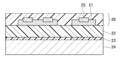
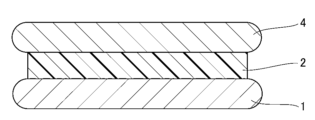
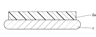
- FIG. 1 is a schematic cross-sectional view of an example of a laminate in the first embodiment A.
- FIG. 2A is a schematic cross-sectional view (part 1) illustrating a method for producing a laminate showing one example of the first embodiment A.
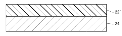
- FIG. 2B is a schematic cross-sectional view (part 2) illustrating a method for producing a laminate showing one example of the first embodiment A.
- FIG. 2C is a schematic cross-sectional view (part 3) illustrating a method for producing a laminate showing one example of the first embodiment A.
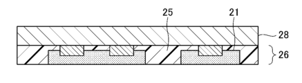
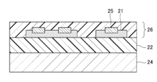
- FIG. 3 is a schematic cross-sectional view of an example of the laminate in the second embodiment A.
- FIG. 4 is a schematic cross-sectional view of another example of the laminate in the second embodiment A.
- FIG. 5A is a schematic cross-sectional view (part 1) illustrating a method for producing a laminate showing one example of the second embodiment A.
- FIG. 5B is a schematic cross-sectional view (part 2) illustrating a method for producing a laminate showing one example of the second embodiment A.
- FIG. 5C is a schematic cross-sectional view (part 3) illustrating a method for producing a laminate showing one example of the second embodiment A.
- FIG. 5D is a schematic cross-sectional view (part 4) illustrating a method for producing a laminate showing one example of the second embodiment A.
- FIG. 6A is a schematic cross-sectional view (part 1) illustrating a method for processing a laminate showing one example of the first embodiment A.
- FIG. 6A is a schematic cross-sectional view (part 1) illustrating a method for processing a laminate showing one example of the first embodiment A.
- FIG. 6B is a schematic cross-sectional view (part 2) illustrating a method for processing the laminate showing one example of the first embodiment A.
- FIG. 6C is a schematic cross-sectional view (part 3) illustrating a method for processing a laminate showing one example of the first embodiment A.
- FIG. 6D is a schematic cross-sectional view (part 4) illustrating a method for processing a laminate showing one example of the first embodiment A.
- FIG. 7A is a schematic cross-sectional view (part 1) illustrating a method for processing a laminate showing one example of the second embodiment A.
- FIG. 7B is a schematic cross-sectional view (part 2) illustrating a method for processing a laminate showing one example of the second embodiment A.
- FIG. 7C is a schematic cross-sectional view (part 3) illustrating a method for processing a laminate showing one example of the second embodiment A.
- FIG. 7D is a schematic cross-sectional view (part 4) illustrating a method for processing a laminate showing one example of the second embodiment A.
- FIG. 7E is a schematic cross-sectional view (part 5) illustrating a method for processing a laminate showing an example of the second embodiment A.
- FIG. 7F is a schematic cross-sectional view (part 6) illustrating a method for processing a laminate showing one example of the second embodiment A.
- FIG. 8 is a schematic cross-sectional view of an example of a laminate in the first embodiment B.
- FIG. 9A is a schematic cross-sectional view (part 1) for explaining a method for producing a laminate showing one example of the first embodiment B.
- FIG. 9B is a schematic cross-sectional view (part 2) for explaining a method for producing a laminate showing one example of the first embodiment B.
- FIG. 10 is a schematic cross-sectional view of an example of a laminate in the second embodiment B.
- FIG. 11A is a schematic cross-sectional view (part 1) for explaining a method for producing a laminate showing one example of the second embodiment B.
- FIG. 11B is a schematic cross-sectional view (part 2) for explaining a method for producing a laminate showing one example of the second embodiment B.
- FIG. 11C is a schematic cross-sectional view (part 3) illustrating a method for producing a laminate showing one example of the second embodiment B.
- FIG. 12A is a schematic cross-sectional view (part 1) illustrating a method for processing a laminate showing one example of the first embodiment B.
- FIG. 12B is a schematic cross-sectional view (part 2) illustrating a method for processing a laminate showing one example of the first embodiment B.
- FIG. 12C is a schematic cross-sectional view (part 3) illustrating a method for processing a laminate showing one example of the first embodiment B.
- FIG. 12D is a schematic cross-sectional view (part 4) illustrating a method for processing a laminate showing an example of the first embodiment B.
- FIG. 12A is a schematic cross-sectional view (part 1) illustrating a method for processing a laminate showing one example of the first embodiment B.
- FIG. 12B is a schematic cross-sectional view (part 2) illustrating a method for processing a laminate showing one example
- FIG. 13A is a schematic cross-sectional view (part 1) illustrating a method for processing a laminate showing one example of the second embodiment B.
- FIG. 13B is a schematic cross-sectional view (part 2) illustrating a method for processing a laminate showing one example of the second embodiment B.
- FIG. 13C is a schematic cross-sectional view (part 3) illustrating a method for processing a laminate showing an example of the second embodiment B.
- FIG. 13D is a schematic cross-sectional view (part 4) illustrating a method for processing a laminate showing an example of the second embodiment B.
- FIG. 13E is a schematic cross-sectional view (part 5) illustrating a method for processing a laminate showing an example of the second embodiment B.
- FIG. 13F is a schematic cross-sectional view (part 6) illustrating a method for processing a laminate showing an example of the second embodiment B.
- the stripping composition for stripping by light irradiation of the present invention contains a novolac resin, a siloxane skeleton-containing epoxy resin, and a solvent.
- the adhesive composition for peeling off by light irradiation of the present invention (hereinafter, may be referred to as "adhesive composition”) contains a novolac resin, a siloxane skeleton-containing epoxy resin, and a solvent. Each component of the release agent composition and the adhesive composition will be described below.
- Novolac resins have at least one of a hydroxy group directly bonded to an aromatic ring and a carboxy group directly bonded to an aromatic ring.
- Novolac resins are resins obtained by, for example, condensation reaction of at least one of a phenolic compound, a carbazole compound, and an aromatic amine compound with at least one of an aldehyde compound, a ketone compound, and a divinyl compound, and optionally with a styrene compound, in the presence of an acid catalyst.
- phenolic compounds include phenols, naphthols, anthrols, and hydroxypyrenes.
- examples of the phenols include phenol, cresol, xylenol, resorcinol, bisphenol A, p-tert-butylphenol, p-octylphenol, 9,9-bis(4-hydroxyphenyl)fluorene, and 1,1,2,2-tetrakis(4-hydroxyphenyl)ethane.
- Examples of the naphthols include 1-naphthol, 2-naphthol, 1,5-dihydroxynaphthalene, 2,7-dihydroxynaphthalene, and 9,9-bis(6-hydroxynaphthyl)fluorene.
- Examples of the anthrols include 9-anthrol.
- Examples of the hydroxypyrenes include 1-hydroxypyrene and 2-hydroxypyrene.
- carbazole compound examples include carbazole, 1,3,6,8-tetranitrocarbazole, 3,6-diaminocarbazole, 3,6-dibromo-9-ethylcarbazole, 3,6-dibromo-9-phenylcarbazole, 3,6-dibromocarbazole, 3,6-dichlorocarbazole, 3-amino-9-ethylcarbazole, 3-bromo-9-ethylcarbazole, 4,4'bis(9H-carbazol-9-yl)biphenyl, 4-glycidylcarbazole, 4-hydroxycarbazole, 9-(1H-benzotriazol-1-yl)phenyl, 4-methyl-1H-phenylcarbazole ...
- aromatic amine compound examples include diphenylamine and N-phenyl-1-naphthylamine. These may be used alone or in combination of two or more. These may have a substituent, for example, a substituent on the aromatic ring.
- aldehyde compounds include saturated aliphatic aldehydes, unsaturated aliphatic aldehydes, heterocyclic aldehydes, aromatic aldehydes, etc.
- saturated aliphatic aldehydes include formaldehyde, paraformaldehyde, acetaldehyde, propylaldehyde, butylaldehyde, isobutyraldehyde, valeraldehyde, capronaldehyde, 2-methylbutyraldehyde, hexylaldehyde, undecanealdehyde, 7-methoxy-3,7-dimethyloctylaldehyde, cyclohexanealdehyde, 3-methyl-2-butylaldehyde, 2-ethylhexylaldehyde, glyoxal, malonaldehyde, succinaldehyde, glutaraldehyde,
- Examples of the unsaturated aliphatic aldehydes include acrolein, methacrolein, etc.
- Examples of heterocyclic aldehydes include furfural, pyridine aldehyde, etc.
- Examples of aromatic aldehydes include benzaldehyde, naphthyl aldehyde, anthryl aldehyde, phenanthryl aldehyde, salicyl aldehyde, phenylacetaldehyde, 3-phenylpropionaldehyde, tolyl aldehyde, (N,N-dimethylamino)benzaldehyde, acetoxybenzaldehyde, etc.
- saturated aliphatic aldehydes and aromatic aldehydes are preferred.
- the ketone compound include diaryl ketone compounds, such as diphenyl ketone, phenyl naphthyl ketone, dinaphthyl ketone, phenyl tolyl ketone, and ditolyl ketone.
- the divinyl compound include divinylbenzene, dicyclopentadiene, tetrahydroindene, 4-vinylcyclohexene, 5-vinylnorborna-2-ene, divinylpyrene, limonene, and 5-vinylnorbornadiene. These may be used alone or in combination of two or more.
- the styrene compound is not particularly limited as long as it is a compound having a styrene structure, and examples thereof include styrene, ⁇ -methylstyrene, hydroxystyrene (vinylphenol), carboxystyrene (vinylbenzoic acid), alkylstyrene, and tertiary-butoxystyrene. These may be used alone or in combination of two or more.
- Novolac resin is, for example, a novolac resin that absorbs light and changes in quality.
- the change is, for example, photodecomposition.
- the novolac resin contains, for example, at least one of a structural unit represented by the following formula (C1-1), a structural unit represented by the following formula (C1-2), and a structural unit represented by the following formula (C1-3).
- the novolac resin may contain at least one structural unit selected from the structural units represented by the following formula (C1-1), the structural units represented by the following formula (1-2), and the structural units represented by the following formula (C1-3).
- C1 represents a group derived from an aromatic compound containing a nitrogen atom.
- C2 represents a group containing a tertiary carbon atom or a quaternary carbon atom having at least one selected from the group consisting of a secondary carbon atom, a quaternary carbon atom, and an aromatic ring in a side chain, or represents a methylene group.
- C3 represents a group derived from an aliphatic polycyclic compound.
- C4 represents a group derived from phenol, a group derived from bisphenol, a group derived from naphthol, a group derived from biphenyl, or a group derived from biphenol.
- C5 represents a single bond or a group having a structure derived from styrene.
- at least one of C 1 , C 2 and C 5 has at least one of a hydroxy group directly bonded to the aromatic ring and a carboxy group directly bonded to the aromatic ring.
- at least one of C 1 , C 3 and C 5 has at least one of a hydroxy group directly bonded to the aromatic ring and a carboxy group directly bonded to the aromatic ring.
- at least one of C 2 , C 4 and C 5 has at least one of a hydroxy group directly bonded to the aromatic ring and a carboxy group directly bonded to the aromatic ring.
- the novolac resin contains, for example, one or more of the following structural units: A structural unit having a bond between a group derived from an aromatic compound containing a nitrogen atom, and a group containing a tertiary or quaternary carbon atom or a methylene group having at least one member selected from the group consisting of a secondary carbon atom, a quaternary carbon atom, and an aromatic ring in a side chain, and optionally a group having a structure derived from styrene (formula (C1-1)).
- a structural unit having a bond between a group derived from an aromatic compound containing a nitrogen atom, and a group containing a tertiary or quaternary carbon atom or a methylene group having at least one member selected from the group consisting of a secondary carbon atom, a quaternary carbon atom, and an aromatic ring in a side chain and optionally a group having a structure derived from styren
- the group derived from an aromatic compound containing a C1 nitrogen atom can be, for example, a group derived from carbazole, a group derived from N-phenyl-1-naphthylamine, a group derived from N-phenyl-2-naphthylamine, a group derived from N,N'-diphenyl-1,4-phenylenediamine, etc., but is not limited thereto.
- the group containing a tertiary or quaternary carbon atom or a methylene group having at least one selected from the group consisting of a secondary carbon atom, a quaternary carbon atom, and an aromatic ring in a side chain of C2 can be, for example, a group derived from 1-naphthaldehyde, a group derived from 1-pyrenecarboxaldehyde, a group derived from 4-(trifluoromethyl)benzaldehyde, a group derived from 2-ethylhexylaldehyde, a group derived from acetaldehyde, or the like, but is not limited thereto.
- the group derived from a C3 aliphatic polycyclic compound can be, but is not limited to, a group derived from dicyclopentadiene.
- C4 is a group derived from phenol, a group derived from bisphenol, a group derived from naphthol, a group derived from biphenyl, or a group derived from biphenol.
- C5 is a single bond or a group having a structure derived from styrene.
- C5 When C5 is a group having a structure derived from styrene, C5 may have at least one of a hydroxy group directly bonded to the aromatic ring and a carboxy group directly bonded to the aromatic ring.
- the novolac resin contains, as the structural unit represented by formula (C1-1), for example, a structural unit represented by the following formula (C1-1-1):
- R 901 and R 902 represent substituents on the ring, and each independently represents a halogen atom, a nitro group, a cyano group, an amino group, an optionally substituted alkyl group, an optionally substituted alkenyl group, or an optionally substituted aryl group.
- R 903 represents a hydrogen atom, an optionally substituted alkyl group, an optionally substituted alkenyl group, or an optionally substituted aryl group.
- R 904 represents a hydrogen atom, an optionally substituted aryl group, or an optionally substituted heteroaryl group.
- R 905 represents an optionally substituted alkyl group, an optionally substituted aryl group, or an optionally substituted heteroaryl group.
- the group of R 904 and the group of R 905 may be bonded to each other to form a divalent group.
- Substituents for the alkyl and alkenyl groups include halogen atoms, nitro groups, cyano groups, amino groups, hydroxy groups, carboxy groups, aryl groups, and heteroaryl groups.
- Substituents for the aryl group and heteroaryl group include a halogen atom, a nitro group, a cyano group, an amino group, a hydroxy group, a carboxy group, an alkyl group, and an alkenyl group.
- X1 and X2 each independently represent a hydroxy group or a carboxy group.
- Z1 represents a single bond or a group having a structure derived from styrene.
- h1 and h2 each independently represent an integer of 0 to 3.
- k1 and k2 each independently represent an integer of 0 to 3.
- the sum of h1 and k1 is less than or equal to 3.
- the sum of h2 and k2 is less than or equal to 3.
- the structural unit represented by formula (C1-1-1) has at least one of a hydroxy group directly bonded to an aromatic ring and a carboxy group directly bonded to an aromatic ring.
- k 1 and k 2 when at least one of R 904 , R 905 and Z 1 has a hydroxy group or a carboxy group, k 1 and k 2 may be 0.
- k 1 and k 2 when at least one of R 904 and R 905 is an aryl group having a hydroxy group or a carboxy group, or when Z 1 has at least one of a hydroxy group directly bonded to the aromatic ring and a carboxy group directly bonded to the aromatic ring, k 1 and k 2 may be 0.
- R 904 and R 905 is an aryl group having a hydroxy group or a carboxy group, or Z 1 has at least one of a hydroxy group directly bonded to the aromatic ring and a carboxy group directly bonded to the aromatic ring.
- the number of carbon atoms in the optionally substituted alkyl group and the optionally substituted alkenyl group is usually 40 or less, and from the viewpoint of solubility, preferably 30 or less, and more preferably 20 or less.
- the number of carbon atoms in an optionally substituted aryl group and heteroaryl group is usually 40 or less, and from the viewpoint of solubility, preferably 30 or less, more preferably 20 or less.
- halogen atoms include fluorine atoms, chlorine atoms, bromine atoms, and iodine atoms.
- examples of the substituent of the optionally substituted alkyl group include a halogen atom, an alkoxy group, a halogenated alkoxy group and the like.
- examples of the substituent of the optionally substituted alkenyl group include a halogen atom, an alkoxy group, a halogenated alkoxy group and the like.
- examples of the substituent of the optionally substituted aryl group include a halogen atom, a hydroxy group, a carboxy group, a cyano group, an alkyl group, a halogenated alkyl group, an alkoxy group, and a halogenated alkoxy group.
- examples of the substituent of the optionally substituted heteroaryl group include a halogen atom, a hydroxy group, a carboxy group, a cyano group, an alkyl group, a halogenated alkyl group, an alkoxy group, and a halogenated alkoxy group.
- alkyl groups which may be substituted include methyl, ethyl, n-propyl, i-propyl, n-butyl, i-butyl, s-butyl, t-butyl, n-pentyl, 1-methyl-n-butyl, 2-methyl-n-butyl, 3-methyl-n-butyl, 1,1-dimethyl-n-propyl, 1,2-dimethyl-n-propyl, 2,2-dimethyl-n-propyl, 1-ethyl-n-propyl, n-hexyl, 1-methyl-n-pentyl, 2-methyl-n-pentyl, 3-methyl-n-pentyl, 4-methyl-n-pentyl, 5-methyl-n-pentyl, 6-methyl-n-pentyl, 7-methyl-n-pentyl, 8-methyl-n-pentyl, 9-methyl-n-pentyl, 10-methyl-n-penty
- alkenyl groups which may be substituted include ethenyl, 1-propenyl, 2-propenyl, 1-methyl-1-ethenyl, 1-butenyl, 2-butenyl, 3-butenyl, 2-methyl-1-propenyl, 2-methyl-2-propenyl, 1-ethylethenyl, 1-methyl-1-propenyl, 1-methyl-2-propenyl, 1-pentenyl, 2-pentenyl, 3-pentenyl, 4-pentenyl, and 1-n-propyl.
- ethenyl group 1-methyl-1-butenyl group, 1-methyl-2-butenyl group, 1-methyl-3-butenyl group, 2-ethyl-2-propenyl group, 2-methyl-1-butenyl group, 2-methyl-2-butenyl group, 2-methyl-3-butenyl group, 3-methyl-1-butenyl group, 3-methyl-2-butenyl group, 3-methyl-3-butenyl group, 1,1-dimethyl-2-propenyl group, 1-i-propylethenyl group, 1,2-dimethyl-1-propenyl group, 1,2-dimethyl a 2-methyl-2-propenyl group, a 1-cyclopentenyl group, a 2-cyclopentenyl group, a 3-cyclopentenyl group, a 1-hexenyl group, a 2-hexenyl group, a 3-hexenyl group, a 4-hexenyl group, a 5-hexenyl group, a 1-methyl-1-penteny
- aryl groups that may be substituted include, but are not limited to, phenyl, 2-methylphenyl, 3-methylphenyl, 4-methylphenyl, 2-chlorophenyl, 3-chlorophenyl, 4-chlorophenyl, 2-fluorophenyl, 3-fluorophenyl, 4-fluorophenyl, 4-methoxyphenyl, 4-ethoxyphenyl, 4-nitrophenyl, 4-cyanophenyl, 2-hydroxyphenyl, 3-hydroxyphenyl, 4-hydroxyphenyl, 2-carboxyphenyl, 3-carboxyphenyl, 4-carboxyphenyl, 4-amyloxyphenyl, 1-naphthyl, 2-naphthyl, biphenyl-4-yl, biphenyl-3-yl, biphenyl-2-yl, 1-anthryl, 2-anthryl, 9-anthryl, 1-phenanthryl, 2-phenanthryl, 3-phenanthryl, 4-phenanthryl, 4-
- optionally substituted heteroaryl groups include, but are not limited to, 2-thienyl, 3-thienyl, 2-furanyl, 3-furanyl, 2-oxazolyl, 4-oxazolyl, 5-oxazolyl, 3-isoxazolyl, 4-isoxazolyl, 5-isoxazolyl, 2-thiazolyl, 4-thiazolyl, 5-thiazolyl, 3-isothiazolyl, 4-isothiazolyl, and 5-isothiazolyl groups.
- Z1 examples include groups represented by the following formula (Z).
- R 910 represents a halogen atom, a nitro group, a cyano group, an amino group, an optionally substituted alkyl group, an optionally substituted alkenyl group or an optionally substituted aryl group.
- R 911 represents a hydrogen atom or a methyl group.
- X10 represents a hydroxy group or a carboxy group.
- h10 and k10 each independently represent an integer of 0 to 3. The sum of h10 and k10 is 5 or less. * represents a bond.
- R 910 include the specific examples given in the description of R 901 and R 902 .
- the novolac resin contains, as the structural unit represented by formula (C1-1), for example, a structural unit represented by the following formula (C1-1-2).
- Ar 901 and Ar 902 each independently represent an aromatic ring, and R 901 to R 905 , X 1 and X 2 , Z 1 , h 1 and h 2 , and k 1 and k 2 have the same meanings as above.
- the sum of h1 and k1 is less than or equal to 3.
- the sum of h2 and k2 is less than or equal to 3.
- n represents an integer of 1 or 2.
- the structural unit represented by formula (C1-1-2) has at least one of a hydroxy group directly bonded to the aromatic ring and a carboxy group directly bonded to the aromatic ring.
- the aromatic ring include a benzene ring and a naphthalene ring.
- k 1 and k 2 when at least one of R 904 , R 905 and Z 1 has a hydroxy group or a carboxy group, k 1 and k 2 may be 0.
- k 1 and k 2 when at least one of R 904 and R 905 is an aryl group having a hydroxy group or a carboxy group, or when Z 1 has at least one of a hydroxy group directly bonded to the aromatic ring and a carboxy group directly bonded to the aromatic ring, k 1 and k 2 may be 0.
- R 904 and R 905 is an aryl group having a hydroxy group or a carboxy group, or Z 1 has at least one of a hydroxy group directly bonded to the aromatic ring and a carboxy group directly bonded to the aromatic ring.
- the novolac resin contains, as the structural unit represented by formula (C1-2), for example, a structural unit represented by the following formula (C1-2-1) or (1-2-2).
- R 906 to R 909 are substituents bonded to the ring, and each independently represents a halogen atom, a nitro group, a cyano group, an amino group, a hydroxy group, a carboxy group, an optionally substituted alkyl group, an optionally substituted alkenyl group, or an optionally substituted aryl group.
- Specific examples and suitable numbers of carbon atoms of the halogen atom, the optionally substituted alkyl group, the optionally substituted alkenyl group, and the optionally substituted aryl group are the same as those described above, and h 3 to h 6 each independently represent an integer of 0 to 3.
- R 901 to R 905 , X 1 and X 2 , Z 1 , h 1 and h 2 , and k 1 and k 2 have the same meanings as defined above.
- the sum of h1 and k1 is less than or equal to 3.
- the sum of h2 and k2 is less than or equal to 3.
- the structural unit represented by formula (C1-2-1) and the structural unit represented by formula (C1-2-2) each independently have at least one of a hydroxy group directly bonded to an aromatic ring and a carboxy group directly bonded to an aromatic ring.
- the novolak resin contains, as the structural unit represented by formula (C1-3), for example, a structural unit represented by the following formula (C1-3-1).
- R 801 represents a substituent on the ring, and each independently represents a halogen atom, a nitro group, a cyano group, an amino group, an optionally substituted alkyl group, an optionally substituted alkenyl group, or an optionally substituted aryl group.
- R 802 represents a hydrogen atom, an optionally substituted aryl group, or an optionally substituted heteroaryl group.
- R 803 represents a hydrogen atom, an optionally substituted alkyl group, an optionally substituted aryl group, or an optionally substituted heteroaryl group.
- the group of R 802 and the group of R 803 may be bonded to each other to form a divalent group.
- Substituents for the aryl group and heteroaryl group include a halogen atom, a nitro group, a cyano group, an amino group, a hydroxy group, a carboxy group, an alkyl group, and an alkenyl group.
- Ar 801 represents a benzene ring, a naphthalene ring, or a biphenyl structure.
- X11 represents a hydroxy group or a carboxy group.
- Z1 represents a single bond or a group having a structure derived from styrene.
- Each of h11 independently represents an integer of 0 to 4.
- Each of k11 independently represents an integer of 0 to 4.
- Ar 801 is a benzene ring, the sum of h 11 and k 11 is 4 or less; when Ar 801 is a naphthalene ring, the sum of h 11 and k 11 is 6 or less; and when Ar 801 is a biphenyl structure, the sum of h 11 and k 11 is 8 or less.
- the structural unit represented by formula (C1-3-1) has at least one of a hydroxy group directly bonded to an aromatic ring and a carboxy group directly bonded to an aromatic ring.
- k 11 when at least one of R 802 , R 803 and Z 1 has a hydroxy group or a carboxy group, k 11 may be 0.
- R 802 and R 803 when at least one of R 802 and R 803 is an aryl group having a hydroxy group or a carboxy group, or when Z 1 has at least one of a hydroxy group directly bonded to the aromatic ring and a carboxy group directly bonded to the aromatic ring, k 11 may be 0.
- R 802 and R 803 when k 11 is 0, at least one of R 802 and R 803 is an aryl group having a hydroxy group or a carboxy group, or a heteroaryl group having a hydroxy group or a carboxy group.
- the novolac resin is a resin obtained by, for example, a condensation reaction of at least one of a phenolic compound, a carbazole compound, and an aromatic amine compound with at least one of an aldehyde compound, a ketone compound, and a divinyl compound, and optionally a styrene compound, in the presence of an acid catalyst.
- the aldehyde compound or ketone compound is usually used in a ratio of 0.1 to 10 equivalents per equivalent of the benzene ring constituting the ring of the carbazole compound.
- the styrene compound as a reaction raw material may have a protecting group.
- An example of a styrene compound having a protecting group is tertiary-butoxystyrene.
- an acid catalyst is usually used.
- the acid catalyst include mineral acids such as sulfuric acid, phosphoric acid, and perchloric acid; organic sulfonic acids such as p-toluenesulfonic acid and p-toluenesulfonic acid monohydrate; and carboxylic acids such as formic acid and oxalic acid, but are not limited to these.
- the amount of the acid catalyst cannot be generally defined since it is appropriately determined depending on the type of acid used, but it is usually appropriately determined within the range of 0.001 to 10,000 parts by mass per 100 parts by mass of the carbazole compound.
- the above condensation reaction can be carried out without using a solvent when either the starting compounds or the acid catalyst used are liquid, but is usually carried out using a solvent.
- a solvent is not particularly limited as long as it does not inhibit the reaction, but typical examples include ether compounds, ether ester compounds, and the like.
- the ether compound include cyclic ether compounds such as tetrahydrofuran and dioxane.
- ether ester compound examples include methyl cellosolve acetate, ethyl cellosolve acetate, butyl cellosolve acetate, propylene glycol monomethyl ether acetate (PGMEA), propylene glycol monoethyl ether acetate, propylene glycol monopropyl ether acetate, propylene glycol monomethyl ether propionate, propylene glycol monoethyl ether propionate, and propylene glycol monopropyl ether propionate.
- PMEA propylene glycol monomethyl ether acetate
- PMEA propylene glycol monoethyl ether acetate
- propylene glycol monopropyl ether acetate propylene glycol monomethyl ether propionate
- propylene glycol monoethyl ether propionate propylene glycol monopropyl ether propionate
- the reaction temperature is usually set appropriately within the range of 40°C to 200°C, and the reaction time cannot be generally determined as it varies depending on the reaction temperature, but is usually set appropriately within the range of 30 minutes to 50 hours.
- novolak resin is used for the preparation of a release agent composition and an adhesive composition.
- a person skilled in the art can determine the production conditions for the novolak resin based on the above explanation and common technical knowledge without excessive burden, and can therefore produce the novolak resin.
- the weight average molecular weight of the novolak resin is usually 500 to 200,000. From the viewpoint of ensuring solubility in a solvent, etc., it is preferably 100,000 or less, more preferably 50,000 or less, even more preferably 10,000 or less, still more preferably 5,000 or less, and even more preferably 3,000 or less. From the viewpoint of improving the strength of the film, etc., it is preferably 600 or more, more preferably 700 or more, even more preferably 800 or more, even more preferably 900 or more, and even more preferably 1,000 or more.
- the weight average molecular weight, number average molecular weight and dispersity of the novolak resin can be measured, for example, using a GPC apparatus (EcoSEC, HLC-8320GPC, manufactured by Tosoh Corporation) and a GPC column (TSKgel SuperMultiporeHZ-N, TSKgel SuperMultiporeHZ-H, manufactured by Tosoh Corporation), at a column temperature of 40° C., using tetrahydrofuran as an eluent (elution solvent), at a flow rate (flow velocity) of 0.35 mL/min, and using polystyrene (manufactured by Sigma-Aldrich Co.) as a standard sample.
- GPC apparatus EuSEC, HLC-8320GPC, manufactured by Tosoh Corporation
- GPC column TSKgel SuperMultiporeHZ-N, TSKgel SuperMultiporeHZ-H, manufactured by Tosoh Corporation
- flow rate flow velocity
- the content of the novolac resin in the stripping composition is not particularly limited, but is preferably 50% by mass to 100% by mass, more preferably 60% by mass to 99% by mass, and particularly preferably 70% by mass to 95% by mass, based on the film-constituting components of the stripping composition.
- the content of the novolac resin in the adhesive composition is not particularly limited, but is preferably 50% by mass to 100% by mass, more preferably 60% by mass to 99% by mass, and particularly preferably 70% by mass to 95% by mass, based on the film-constituting components of the adhesive composition.
- the film constituent components refer to components other than the solvent contained in the composition.
- the siloxane skeleton-containing epoxy resin has a siloxane bond and an epoxy group.
- the siloxane skeleton-containing epoxy resin has, for example, two or more silicon atoms, and preferably has four or more silicon atoms.
- the siloxane skeleton-containing epoxy resin may be linear or cyclic.
- the siloxane skeleton-containing epoxy resin preferably contains a structure represented by the following formula (A).
- R 1 represents a substituted or unsubstituted alkyl group, a substituted or unsubstituted alkenyl group, or a substituted or unsubstituted aryl group.
- R 2 represents an alkylene group having 1 to 10 carbon atoms.
- Y represents a single bond or -O-.
- Ep represents a group represented by the following formula (A-1) or formula (A-2). * represents a bond.)
- * represents a bond.
- alkyl group in the "substituted or unsubstituted alkyl group” of R 1 in formula (A) is preferably an alkyl group having 1 to 10 carbon atoms.
- alkyl group include a methyl group, an ethyl group, a propyl group, an isopropyl group, a butyl group, an isobutyl group, a sec-butyl group, a tert-butyl group, a pentyl group, an isopentyl group, a neopentyl group, a sec-pentyl group, a tert-pentyl group, a cyclopentyl group, a cyclohexyl group, a cyclopentylmethyl group, a 2-cyclohexylmethyl group, a 2-cyclopentylethyl group, and a 2-cyclohexylethyl group.
- alkenyl group in the "substituted or unsubstituted alkenyl group” of R 1 in formula (A) is preferably an alkenyl group having 2 to 10 carbon atoms.
- alkenyl group include a vinyl group, a 1-propenyl group, a 2-propenyl group, a 2-methyl-1-propenyl group, a 1-butenyl group, a 2-butenyl group, a 3-butenyl group, a 3-methyl-2-butenyl group, a 1-pentenyl group, a 2-pentenyl group, a 3-pentenyl group, a 4-pentenyl group, a 4-methyl-3-pentenyl group, a 1-hexenyl group, a 3-hexenyl group, a 5-hexenyl group, and a 2-cyclohexenyl group.
- the substituent of the alkyl group in the "substituted or unsubstituted alkyl group" of R 1 in formula (A) and the substituent of the alkenyl group in the "substituted or unsubstituted alkenyl group” are not particularly limited, and examples thereof include a halogen atom, a cyano group, a nitro group, an alkyl-oxy group, an alkyl-carbonyl group, an alkyl-oxy-carbonyl group, an alkyl-carbonyl-oxy group, an alkenyl-oxy group, an alkenyl-carbonyl group, an alkenyl-oxy-carbonyl group, an alkenyl-carbonyl-oxy group, an alkenyl-carbonyl-oxy group, an aryl group, an aryl-oxy group, an aryl-carbonyl group, an aryl-oxy-carbonyl group, an aryl-carbonyl-oxy group, and the like, or
- the "aryl group” in the "substituted or unsubstituted aryl group” of R 1 in formula (A) is preferably an aryl group having 6 to 14 carbon atoms.
- Examples of the "aryl group” include a phenyl group, a 1-naphthyl group, and a 2-naphthyl group.
- the substituent of the aryl group in the "substituted or unsubstituted aryl group" of R 1 is not particularly limited, but examples thereof include a halogen atom, a cyano group, a nitro group, an alkyl group, an alkyl-oxy group, an alkyl-carbonyl group, an alkyl-oxy-carbonyl group, an alkyl-carbonyl-oxy group, an alkenyl group, an alkenyl-oxy group, an alkenyl-carbonyl group, an alkenyl-oxy-carbonyl group, an alkenyl-carbonyl-oxy group, an aryl group, an aryl-alkyl group, an aryl-alkenyl group, an aryl-oxy group, an aryl-carbonyl group, an aryl-oxy-carbonyl group, an aryl-carbonyl-oxy group, and the like, or a combination thereof.
- the number of the substituents is preferably
- halogen atom includes, for example, a fluorine atom, a chlorine atom, a bromine atom, and the like.
- R 1 in formula (A) is preferably a substituted or unsubstituted alkyl group, more preferably an (unsubstituted) alkyl group, further more preferably a methyl group, an ethyl group, a propyl group, or an isopropyl group, and particularly preferably a methyl group.
- the siloxane skeleton-containing epoxy resin is preferably represented by any one of the following formulas (SE1) to (SE3), for example.
- the repeating units may be arranged randomly.
- R 101 to R 110 each independently represent a substituted or unsubstituted alkyl group, a substituted or unsubstituted alkenyl group, or a substituted or unsubstituted aryl group.
- X 101 represents a group represented by formula (EA) below.
- Y 101 represents a hydrogen atom, a hydroxy group, or a monovalent group having 1 to 30 carbon atoms (however, different from X 101 ).
- l represents 0 or an integer of 1 or more.
- m represents an integer of 1 or more.
- n represents 0 or an integer of 1 or more.
- R 201 to R 207 each independently represent a substituted or unsubstituted alkyl group, a substituted or unsubstituted alkenyl group, or a substituted or unsubstituted aryl group.
- X 201 and X 202 each independently represent a group represented by the following formula (EA).
- Y 201 represents a hydrogen atom, a hydroxyl group, or a monovalent group having 1 to 30 carbon atoms.
- l represents 0 or an integer of 1 or more.
- m represents 0 or an integer of 1 or more.
- R 301 to R 304 each independently represent a substituted or unsubstituted alkyl group, a substituted or unsubstituted alkenyl group, or a substituted or unsubstituted aryl group.
- X 301 to X 304 each independently represent a group represented by the following formula (EA).
- m represents an integer of 1 to 3.
- R2 represents an alkylene group having 1 to 10 carbon atoms.
- Y represents a single bond or -O-.
- Ep represents a group represented by formula (A-1) or (A-2) below. * represents a bond.) (In formula (A-1) and formula (A-2), * represents a bond.)
- substituted or unsubstituted alkyl group, substituted or unsubstituted alkenyl group, and substituted or unsubstituted aryl group of R 101 to R 110 in formula (SE1), R 201 to R 207 in formula (SE2), and R 301 to R 304 in formula (SE3) include the specific and suitable examples in the description of R 1 in formula (A).
- examples of the monovalent group having 1 to 30 carbon atoms for Y 101 and Y 201 include monovalent groups represented by any one of the following (i) to (iv).
- a hydrocarbon group having 7 to 30 carbon atoms a monovalent hydrocarbon group having 2 to 30 carbon atoms, which is constituted by at least one of an ether bond, a thioether bond, an amide bond, a urethane bond, and an ester bond being inserted between the carbon-carbon bonds of the hydrocarbon group;
- a monovalent hydrocarbon group having 2 to 30 carbon atoms which is constituted by at least one of an ether bond, a thioether bond, an amide bond, a
- siloxane skeleton-containing epoxy resin examples include as follows.
- Epoxy resins containing a chain siloxane skeleton such as 1,3,5-tris(2-(3,4-epoxycyclohexyl)ethyl)-1,1,3,5,5-pentamethyltrisiloxane;
- Epoxy resins containing a cyclic siloxane skeleton such as 2,4,6,8-tetrakis(4-(3,4-epoxycyclopentyl)butyl)-2,4,6,8-tetramethylcyclotetrasiloxane, 2,4,6,8-tetrakis(3-(3,4-epoxycyclopentyl)propyl)-2,4,6,8-tetramethylcyclotetrasiloxane, 2,4,6,8-tetrakis(2-(3,4-epoxycyclohexyl)ethyl)-2,4,6,8-tetramethylcyclotetrasiloxane,
- the molecular weight of the siloxane skeleton-containing epoxy resin is not particularly limited, but the upper limit is preferably 15,000 or less, more preferably 10,000 or less, even more preferably 8,000 or less, and particularly preferably 5,000 or less.
- the lower limit can be, for example, 200 or more, 400 or more, 600 or more, etc.
- the epoxy equivalent of the siloxane skeleton-containing epoxy resin is not particularly limited, but the upper limit is preferably 1,000 g/eq. or less, more preferably 500 g/eq. or less, even more preferably 300 g/eq. or less, and particularly preferably 250 g/eq. or less.
- the lower limit is preferably 50 g/eq. or more, more preferably 100 g/eq. or more, even more preferably 130 g/eq. or more, and particularly preferably 150 g/eq. or more.
- the siloxane skeleton-containing epoxy resin may be a commercially available product.
- commercially available products include "KF-105", “KF-1005”, and “KR-470” (main component: 2,4,6,8-tetrakis(2-(3,4-epoxycyclohexyl)ethyl)-2,4,6,8-tetramethylcyclotetrasiloxane) and "X-40-2667” (main component: 1,3,5-tris(2-(3,4-epoxycyclohexyl)ethyl)-1,1,3,5,5-pentamethyltrisiloxane) manufactured by Shin-Etsu Chemical Co., Ltd., and "EP-3400L” manufactured by ADEKA Corporation.
- the viscosity (25°C) of the siloxane skeleton-containing epoxy resin is not particularly limited, but is preferably 100 mPa ⁇ s to 10,000 mPa ⁇ s, and more preferably 1,000 mPa ⁇ s to 5,000 mPa ⁇ s.
- the content of the siloxane skeleton-containing epoxy resin in the release agent composition is not particularly limited, but is preferably 1% by mass to 70% by mass, more preferably 3% by mass to 55% by mass, and particularly preferably 5% by mass to 40% by mass, based on the novolac resin in the release agent composition.
- the content of the siloxane skeleton-containing epoxy resin in the adhesive composition is not particularly limited, but is preferably 1 mass % to 70 mass %, more preferably 3 mass % to 55 mass %, and particularly preferably 5 mass % to 40 mass %, relative to the novolac resin in the adhesive composition.
- the release agent composition may contain a curing catalyst.
- the adhesive composition may contain a curing catalyst.
- the curing catalyst is not particularly limited, but examples thereof include amines, imidazoles, organic phosphines, Lewis acids, and the like.
- examples of the amines include tertiary amines, such as 1,8-diazabicyclo(5.4.0)undec-7-ene (DBU), triethylenediamine, benzyldimethylamine, triethanolamine, dimethylaminoethanol, and tris(dimethylaminomethyl)phenol.
- DBU 1,8-diazabicyclo(5.4.0)undec-7-ene
- Examples of the imidazoles include 2-methylimidazole, 2-phenylimidazole, 2-ethyl-4-methylimidazole, 4-methyl-2-phenylimidazole, 2-heptadecylimidazole, and 2-phenyl-1-benzyl-1H-imidazole.
- Examples of the organic phosphines include tributylphosphine, methyldiphenylphosphine, triphenylphosphine, diphenylphosphine, and phenylphosphine.
- curing catalysts include, for example, tetra-substituted phosphonium tetra-substituted borates such as tetraphenylphosphonium tetraphenylborate, tetraphenylphosphonium ethyltriphenylborate, and tetrabutylphosphonium tetrabutylborate; tetraphenylboron salts such as 2-ethyl-4-methylimidazole tetraphenylborate and N-methylmorpholine tetraphenylborate; and tetrabutylphosphonium O,O-diethylphosphorodithioate.
- tetra-substituted phosphonium tetra-substituted borates such as tetraphenylphosphonium tetraphenylborate, tetraphenylphosphonium ethyltriphenylborate, and t
- the amount of the curing catalyst contained in the release agent composition is not particularly limited, but is preferably 1% by mass to 20% by mass relative to the siloxane skeleton-containing epoxy resin in the release agent composition.
- the amount of the curing catalyst contained in the adhesive composition is not particularly limited, but is preferably 1% by mass to 20% by mass relative to the siloxane skeleton-containing epoxy resin in the adhesive composition.
- the release agent composition and the adhesive composition may contain a surfactant for the purposes of adjusting the liquid properties of the composition itself and the film properties of the resulting film, and for the purpose of preparing a highly uniform release agent composition and an adhesive composition with good reproducibility.
- the surfactant examples include polyoxyethylene alkyl ethers such as polyoxyethylene lauryl ether, polyoxyethylene stearyl ether, polyoxyethylene cetyl ether, and polyoxyethylene oleyl ether; polyoxyethylene alkyl allyl ethers such as polyoxyethylene octyl phenol ether and polyoxyethylene nonyl phenol ether; polyoxyethylene-polyoxypropylene block copolymers; sorbitan fatty acid esters such as sorbitan monolaurate, sorbitan monopalmitate, sorbitan monostearate, sorbitan monooleate, sorbitan trioleate, and sorbitan tristearate; polyoxyethylene sorbitan monolaurate, polyoxyethylene sorbitan monopalmitate,
- the surfactant include nonionic surfactants such as polyoxyethylene sorbitan fatty acid esters, such as polyoxyethylene sorbitan monostearate, polyoxyethylene sorbitan trioleate, and poly
- the surfactants can be used alone or in combination of two or more.
- the amount of the surfactant in the stripping composition is usually 2% by mass or less based on the film-constituting components of the stripping composition.
- the amount of the surfactant in the adhesive composition is usually 2 mass % or less based on the film-constituting components of the adhesive composition.
- the stripper composition includes a solvent.
- the adhesive composition includes a solvent.
- the solvent for example, a high polarity solvent capable of dissolving well the film constituent components such as the above-mentioned novolac resin and siloxane skeleton-containing epoxy resin can be used, and a low polarity solvent may be used as necessary for the purpose of adjusting viscosity, surface tension, etc.
- a low polarity solvent is defined as a solvent having a relative dielectric constant of less than 7 at a frequency of 100 kHz
- a high polarity solvent is defined as a solvent having a relative dielectric constant of 7 or more at a frequency of 100 kHz.
- the solvents can be used alone or in combination of two or more.
- highly polar solvents include amide-based solvents such as N,N-dimethylformamide, N,N-dimethylacetamide, N,N-dimethylisobutyramide, N-methylpyrrolidone, and 1,3-dimethyl-2-imidazolidinone; ketone-based solvents such as ethyl methyl ketone, isophorone, and cyclohexanone; cyano-based solvents such as acetonitrile and 3-methoxypropionitrile; polyhydric alcohol-based solvents such as ethylene glycol, diethylene glycol, triethylene glycol, dipropylene glycol, 1,3-butanediol, and 2,3-butanediol; Examples of the solvent include monohydric alcohol solvents other than aliphatic alcohols, such as propylene glycol monomethyl ether, diethylene glycol monomethyl ether, diethylene glycol monophenyl ether, triethylene glycol monomethyl ether, dipropylene
- low polarity solvents include chlorine-based solvents such as chloroform and chlorobenzene; aromatic hydrocarbon-based solvents such as alkylbenzenes such as toluene, xylene, tetralin, cyclohexylbenzene, and decylbenzene; aliphatic alcohol-based solvents such as 1-octanol, 1-nonanol, and 1-decanol; ether-based solvents such as tetrahydrofuran, dioxane, anisole, 4-methoxytoluene, 3-phenoxytoluene, dibenzyl ether, diethylene glycol dimethyl ether, diethylene glycol butyl methyl ether, triethylene glycol dimethyl ether, and triethylene glycol butyl methyl ether; and ester-based solvents such as methyl benzoate, ethyl benzoate, butyl benzoate, isoamyl benzoate, bis(2-ethyl
- the amount of solvent is appropriately determined taking into consideration the viscosity of the desired composition, the coating method to be used, the thickness of the film to be produced, etc., but is 99% by mass or less of the entire composition, preferably 70 to 99% by mass, and more preferably 85 to 97% by mass of the entire composition; in other words, the amount of the film components in this case is preferably 1 to 30% by mass, and more preferably 3 to 15% by mass of the entire composition.
- the viscosity and surface tension of the stripping agent composition and adhesive composition are appropriately adjusted by changing the types of solvents used, their ratios, the concentrations of the film constituent components, etc., taking into consideration various factors such as the application method used and the desired film thickness.
- the release agent composition and adhesive composition contain a glycol-based solvent from the viewpoint of reproducibly obtaining a highly uniform composition, a highly storage stable composition, and a composition that gives a highly uniform film.
- glycol-based solvent here is a general term for glycols, glycol monoethers, glycol diethers, glycol monoesters, glycol diesters, and glycol ester ethers.
- R G1 each independently represents a linear or branched alkylene group having 2 to 4 carbon atoms
- R G2 and R G3 each independently represent a hydrogen atom, a linear or branched alkyl group having 1 to 8 carbon atoms, or an alkylacyl group in which the alkyl portion is a linear or branched alkyl group having 1 to 8 carbon atoms
- n g is an integer from 1 to 6.
- linear or branched alkylene group having 2 to 4 carbon atoms include, but are not limited to, an ethylene group, a trimethylene group, a 1-methylethylene group, a tetramethylene group, a 2-methylpropane-1,3-diyl group, a pentamethylene group, and a hexamethylene group.
- a linear or branched alkylene group having 2 to 3 carbon atoms is preferred, and a linear or branched alkylene group having 3 carbon atoms is more preferred.
- linear or branched alkyl group having 1 to 8 carbon atoms include a methyl group, an ethyl group, an n-propyl group, an i-propyl group, an n-butyl group, an i-butyl group, an s-butyl group, a tertiary butyl group, an n-pentyl group, a 1-methyl-n-butyl group, a 2-methyl-n-butyl group, a 3-methyl-n-butyl group, a 1,1-dimethyl-n-propyl group, a 1,2-dimethyl-n-propyl group, a 2,2-dimethyl-n-propyl group, a 1-ethyl-n-propyl group, an n-hexyl group, a 1-methyl-n-pentyl group, a 2-methyl-n-pentyl group, a 3-methyl
- dimethyl-n-butyl groups include, but are
- a methyl group and an ethyl group are preferred, and a methyl group is more preferred.
- linear or branched alkyl group having 1 to 8 carbon atoms in the alkyl acyl group in which the alkyl portion is a linear or branched alkyl group having 1 to 8 carbon atoms include the same as the specific examples mentioned above.
- a methylcarbonyl group and an ethylcarbonyl group are preferred, and a methylcarbonyl group is more preferred.
- n g is preferably 4 or less, more preferably 3 or less, even more preferably 2 or less, and most preferably 1.
- R G2 and R G3 are a linear or branched alkyl group having 1 to 8 carbon atoms, and more preferably, one of R G2 and R G3 is a linear or branched alkyl group having 1 to 8 carbon atoms, and the other is a hydrogen atom or an alkyl acyl group in which the alkyl moiety is a linear or branched alkyl group having 1 to 8 carbon atoms.
- the content of the glycol-based solvent in the release agent composition is preferably 50% by mass or more, more preferably 70% by mass or more, even more preferably 80% by mass or more, even more preferably 90% by mass or more, and even more preferably 95% by mass or more, based on the solvent contained in the release agent composition.
- the film constituent components are uniformly dispersed or dissolved in the solvent, and preferably dissolved.
- the content of the glycol-based solvent in the adhesive composition is preferably 50 mass % or more, more preferably 70 mass % or more, even more preferably 80 mass % or more, even more preferably 90 mass % or more, and even more preferably 95 mass % or more, relative to the solvent contained in the adhesive composition.
- the film constituent components are uniformly dispersed or dissolved in the solvent, and preferably dissolved.
- the solvents, solutions, etc. used may be filtered using a filter during the production of the release agent composition and adhesive composition or after all the components have been mixed.
- Embodiment A of the laminate according to the present invention comprises a semiconductor substrate or an electronic device layer, a supporting substrate, and a release agent layer for peeling by light irradiation.
- Embodiment A of the laminate according to the present invention preferably further comprises an adhesive layer, and has a configuration comprising a semiconductor substrate or electronic device layer, a supporting substrate, a release agent layer for peeling by light irradiation, and an adhesive layer.
- the laminate may be formed of a single-layer structure of the release agent layer having adhesive performance, rather than a two-layer structure of the release agent layer and the adhesive layer.
- the supporting substrate is optically transparent.
- the release agent layer for light irradiation peeling is provided between the semiconductor substrate or electronic device layer and the supporting substrate.
- the embodiment A of the laminate is used in such a manner that the semiconductor substrate or electronic device layer and the supporting substrate are peeled off after the release agent layer absorbs light irradiated from the supporting substrate side.
- the release agent layer for peeling off by light irradiation is a layer formed from the above-mentioned release agent composition for peeling off by light irradiation of the present invention.
- Embodiment A of the laminate of the present invention is used for temporary bonding for processing a semiconductor substrate or an electronic device layer, and can be suitably used for processing such as thinning a semiconductor substrate or an electronic device layer.
- the semiconductor substrate is supported by the support substrate.
- the release agent layer is irradiated with light, and then the support substrate and the semiconductor substrate are separated.
- the novolac resin contained in the release agent composition for light irradiation peeling of the present invention absorbs light (e.g., laser light) in the release agent layer formed from the release agent composition, and alters the release agent layer (e.g., separates or decomposes).
- the release agent layer is irradiated with light
- the semiconductor substrate and the support substrate are easily peeled off.
- the electronic device layer is supported by the support substrate.
- the release agent layer is irradiated with light, and then the support substrate and the electronic device layer are separated from each other.
- the release agent layer according to the present invention facilitates peeling of the semiconductor substrate or electronic device layer from the supporting substrate after irradiation with light.
- residues of the release agent layer or adhesive layer remaining on the semiconductor substrate, electronic device layer, or supporting substrate after the semiconductor substrate or electronic device layer is peeled from the supporting substrate can be removed, for example, with a cleaning composition for cleaning semiconductor substrates and the like.
- the wavelength of the light used for peeling is, for example, preferably 250 to 600 nm, more preferably 250 to 370 nm. More preferably, the wavelength is 308 nm, 343 nm, 355 nm, 365 nm, or 532 nm.
- the amount of light required for peeling is an amount that can cause suitable alteration, such as decomposition, of the novolac resin.
- the light used for the peeling may be laser light or non-laser light emitted from a light source such as an ultraviolet lamp.
- the laminated body will be described in detail below, with respect to the case where the laminated body includes a semiconductor substrate and the case where the laminated body includes an electronic device layer.
- the case where the laminate has a semiconductor substrate is described below in ⁇ First embodiment A>, and the case where the laminate has an electronic device layer is described below in ⁇ Second embodiment A>.
- the laminate having the semiconductor substrate is used for processing the semiconductor substrate. During the processing of the semiconductor substrate, the semiconductor substrate is adhered to the support substrate. After the processing of the semiconductor substrate, the release agent layer is irradiated with light, and then the semiconductor substrate is separated from the support substrate.
- the main material constituting the entire semiconductor substrate is not particularly limited as long as it is used for this type of application, but examples thereof include silicon, silicon carbide, and compound semiconductors.
- the shape of the semiconductor substrate is not particularly limited, but may be, for example, a disk shape. Note that the disk-shaped semiconductor substrate does not need to have a perfectly circular surface, and for example, the outer periphery of the semiconductor substrate may have a straight line portion called an orientation flat, or may have a cut called a notch.
- the thickness of the disk-shaped semiconductor substrate may be appropriately determined depending on the intended use of the semiconductor substrate, and is not particularly limited, but is, for example, 500 to 1,000 ⁇ m.
- the diameter of the disk-shaped semiconductor substrate may be appropriately determined depending on the intended use of the semiconductor substrate, and is not particularly limited, but is, for example, 100 to 1,000 mm.
- the semiconductor substrate may have bumps, which are protruding terminals.
- the semiconductor substrate when the semiconductor substrate has bumps, the semiconductor substrate has the bumps on the supporting substrate side.
- bumps are usually formed on a surface on which a circuit is formed.
- the circuit may be a single layer or a multilayer.
- the surface opposite to the surface having the bumps (back surface) is the surface to be processed.
- the material, size, shape, structure, and density of the bumps on the semiconductor substrate are not particularly limited. Examples of the bump include a ball bump, a printed bump, a stud bump, and a plated bump.
- the height, radius and pitch of the bumps are appropriately determined based on the conditions of a bump height of about 1 to 200 ⁇ m, a bump radius of 1 to 200 ⁇ m and a bump pitch of 1 to 500 ⁇ m.
- materials for the bump include low melting point solder, high melting point solder, tin, indium, gold, silver, copper, etc.
- the bump may be composed of only a single component, or may be composed of multiple components. More specifically, examples of the bump include alloy plating mainly composed of Sn, such as SnAg bump, SnBi bump, Sn bump, and AuSn bump.
- the bump may have a laminated structure including a metal layer made of at least one of these components.
- An example of a semiconductor substrate is a silicon wafer with a diameter of about 300 mm and a thickness of about 770 ⁇ m.
- the supporting substrate is not particularly limited as long as it is optically transparent to the light irradiated onto the release agent layer and is capable of supporting the semiconductor substrate when the semiconductor substrate is processed.
- a glass supporting substrate can be used.
- the shape of the support substrate is not particularly limited, but may be, for example, a disk shape.
- the thickness of the disk-shaped support substrate may be appropriately determined depending on the size of the semiconductor substrate, and is not particularly limited, but is, for example, 500 to 1,000 ⁇ m.
- the diameter of the disk-shaped support substrate may be appropriately determined depending on the size of the semiconductor substrate, and is not particularly limited, but is, for example, 100 to 1,000 mm.
- An example of a support substrate is a glass wafer with a diameter of about 300 mm and a thickness of about 700 ⁇ m.
- the release agent layer is a layer formed from a release agent composition.
- the release agent layer is provided between the semiconductor substrate and the supporting substrate.
- the release agent layer may be in contact with either the supporting substrate or the semiconductor substrate.
- the release agent layer is formed using the above-mentioned release agent composition for photo-exposure peeling of the present invention.
- the release agent composition of the present invention can be suitably used for forming a release agent layer of a laminate having a semiconductor substrate, a support substrate, and a release agent layer provided between the semiconductor substrate and the support substrate.
- the laminate is used in such a manner that the semiconductor substrate and the support substrate are peeled off after the release agent layer absorbs light irradiated from the support substrate side.
- One of the features of the release agent layer obtained from the release agent composition of the present invention is that the semiconductor substrate and the supporting substrate can be easily peeled off after irradiation with light.
- the novolac resin is thought to react with the siloxane skeleton-containing epoxy resin.
- the thickness of the release agent layer is not particularly limited, but is usually 0.05 to 3 ⁇ m. From the viewpoint of maintaining the film strength, the thickness is preferably 0.07 ⁇ m or more, more preferably 0.1 ⁇ m or more, and even more preferably 0.2 ⁇ m or more. From the viewpoint of avoiding non-uniformity due to a thick film, the thickness is preferably 2 ⁇ m or less, more preferably 1 ⁇ m or less, even more preferably 0.8 ⁇ m or less, and even more preferably 0.5 ⁇ m or less.
- the method for forming the release agent layer from the release agent composition will be described in detail in the description of ⁇ An example of a method for producing the laminate in the first embodiment A>> below.
- the adhesive layer is provided between the support substrate and the semiconductor substrate.
- the adhesive layer may be in contact with, for example, a semiconductor substrate.
- the adhesive layer may be in contact with, for example, a support substrate.
- the adhesive layer is not particularly limited, but is preferably a layer formed from an adhesive composition.
- Adhesive composition examples include, but are not limited to, polysiloxane-based adhesives, acrylic resin-based adhesives, epoxy resin-based adhesives, polyamide-based adhesives, polystyrene-based adhesives, polyimide adhesives, phenolic resin-based adhesives, and the like.
- polysiloxane-based adhesives are preferred as the adhesive composition, because they exhibit suitable adhesive performance during processing of semiconductor substrates and the like, can be suitably peeled off after processing, have excellent heat resistance, and can be suitably removed by a cleaning composition.
- the adhesive composition here is usually not the photoirradiation peelable adhesive composition of the present invention.
- the adhesive composition contains a polyorganosiloxane. In another preferred embodiment, the adhesive composition includes a component that cures via a hydrosilylation reaction.
- the adhesive composition used in the present invention contains a curable component (A) that becomes an adhesive component.
- the adhesive composition used in the present invention may contain a curable component (A) that becomes an adhesive component and a component (B) that does not undergo a curing reaction.
- an example of the component (B) that does not undergo a curing reaction is polyorganosiloxane.
- "does not cause a curing reaction” does not mean that any curing reaction does not occur, but means that the curing reaction occurring in the curable component (A) does not occur.
- component (A) may be a component that cures by a hydrosilylation reaction, or may be a polyorganosiloxane component (A') that cures by a hydrosilylation reaction.
- component (A) contains, for example, polyorganosiloxane (a1) having an alkenyl group having 2 to 40 carbon atoms bonded to a silicon atom, as an example of component (A'), polyorganosiloxane (a2) having a Si-H group, and platinum group metal catalyst (A2).
- the alkenyl group having 2 to 40 carbon atoms may be substituted.
- the substituent include a halogen atom, a nitro group, a cyano group, an amino group, a hydroxyl group, a carboxyl group, an aryl group, and a heteroaryl group.
- the polyorganosiloxane component (A' ) that cures by a hydrosilylation reaction comprises a polysiloxane ( A1 ) containing one or more units selected from the group consisting of siloxane units represented by SiO2 (Q units), siloxane units represented by R1R2R3SiO1/2 ( M units ), siloxane units represented by R4R5SiO2 / 2 (D units ) , and siloxane units represented by R6SiO3/2 ( T units ), and a platinum group metal catalyst ( A2 ).
- R 1 to R 6 are groups or atoms bonded to the silicon atom, and each independently represents an optionally substituted alkyl group, an optionally substituted alkenyl group, or a hydrogen atom.
- substituents include a halogen atom, a nitro group, a cyano group, an amino group, a hydroxyl group, a carboxyl group, an aryl group, and a heteroaryl group.
- R 1 ' to R 6 ' are groups bonded to a silicon atom and each independently represents an optionally substituted alkyl group or an optionally substituted alkenyl group, with at least one of R 1 ' to R 6 ' being an optionally substituted alkenyl group.
- substituents include a halogen atom, a nitro group, a cyano group, an amino group, a hydroxyl group, a carboxyl group, an aryl group, and a heteroaryl group.
- R 1 ′′ to R 6 ′′ are groups or atoms bonded to the silicon atom and each independently represents an optionally substituted alkyl group or a hydrogen atom, with at least one of R 1 ′′ to R 6 ′′ being a hydrogen atom.
- substituents include a halogen atom, a nitro group, a cyano group, an amino group, a hydroxyl group, a carboxyl group, an aryl group, and a heteroaryl group.
- the alkyl group may be linear, branched, or cyclic, but linear or branched alkyl groups are preferred, and the number of carbon atoms is not particularly limited, but is usually 1 to 40, preferably 30 or less, more preferably 20 or less, and even more preferably 10 or less.
- optionally substituted straight-chain or branched-chain alkyl groups include methyl, ethyl, n-propyl, i-propyl, n-butyl, i-butyl, s-butyl, tertiary butyl, n-pentyl, 1-methyl-n-butyl, 2-methyl-n-butyl, 3-methyl-n-butyl, 1,1-dimethyl-n-propyl, 1,2-dimethyl-n-propyl, 2,2-dimethyl-n-propyl, 1-ethyl-n-propyl, n-hexyl, 1-methyl-n-pentyl, 2-methyl-n-pentyl, 3-methyl-n-pentyl, 4-methyl-n-pentyl, and 5-methyl-n-pentyl.
- alkyl group examples include, but are not limited to, 1,1-dimethyl-n-butyl, 1,2-dimethyl-n-butyl, 1,3-dimethyl-n-butyl, 2,2-dimethyl-n-butyl, 2,3-dimethyl-n-butyl, 3,3-dimethyl-n-butyl, 1-ethyl-n-butyl, 2-ethyl-n-butyl, 1,1,2-trimethyl-n-propyl, 1,2,2-trimethyl-n-propyl, 1-ethyl-1-methyl-n-propyl, and 1-ethyl-2-methyl-n-propyl groups.
- the number of carbon atoms is usually 1 to 14, preferably 1 to 10, and more preferably 1 to 6.
- the methyl group is particularly preferred.
- optionally substituted cyclic alkyl groups include cyclopropyl, cyclobutyl, 1-methylcyclopropyl, 2-methylcyclopropyl, cyclopentyl, 1-methylcyclobutyl, 2-methylcyclobutyl, 3-methylcyclobutyl, 1,2-dimethylcyclopropyl, 2,3-dimethylcyclopropyl, 1-ethylcyclopropyl, 2-ethylcyclopropyl, cyclohexyl, 1-methylcyclopentyl, 2-methylcyclopentyl, 3-methylcyclopentyl, 1-ethylcyclobutyl, 2-ethylcyclobutyl, 3-ethylcyclobutyl, 1,2-dimethylcyclobutyl, 1,3-dimethylcyclobutyl, 2,2-dimethylcyclobutyl, 2,3-dimethylcyclobutyl, 2,4-dimethylcyclobutyl, 3,3-dimethylcyclobutyl, 3,
- the alkenyl group may be either linear or branched, and the number of carbon atoms is not particularly limited, but is usually 2 to 40, preferably 30 or less, more preferably 20 or less, and even more preferably 10 or less.
- the optionally substituted linear or branched alkenyl group include, but are not limited to, a vinyl group, an allyl group, a butenyl group, a pentenyl group, and the like, and the number of carbon atoms is usually 2 to 14, preferably 2 to 10, and more preferably 1 to 6. Among these, an ethenyl group and a 2-propenyl group are particularly preferred.
- Specific examples of the optionally substituted cyclic alkenyl group include, but are not limited to, cyclopentenyl, cyclohexenyl, and the like, and the number of carbon atoms is usually 4 to 14, preferably 5 to 10, and more preferably 5 to 6.
- polysiloxane (A1) contains polyorganosiloxane (a1') and polyorganosiloxane (a2'), and the alkenyl groups contained in polyorganosiloxane (a1') and the hydrogen atoms (Si-H groups) contained in polyorganosiloxane (a2') form a crosslinked structure through a hydrosilylation reaction caused by a platinum group metal catalyst (A2), and the crosslinked structure hardens. As a result, a hardened film is formed.
- Polyorganosiloxane (a1') contains one or more units selected from the group consisting of Q' units, M' units, D' units, and T' units, and also contains at least one unit selected from the group consisting of M' units, D' units, and T' units.
- polyorganosiloxane (a1') a combination of two or more polyorganosiloxanes satisfying such conditions may be used.
- Q' units, M' units, D' units and T' units include, but are not limited to, (Q' units and M' units), (D' units and M' units), (T' units and M' units), and (Q' units, T' units and M' units).
- the polyorganosiloxane (a1') contains two or more types of polyorganosiloxane, combinations of (Q' units and M' units) and (D' units and M' units), combinations of (T' units and M' units) and (D' units and M' units), and combinations of (Q' units, T' units and M' units) and (T' units and M' units) are preferred, but are not limited to these.
- Polyorganosiloxane (a2') contains one or more units selected from the group consisting of Q" units, M" units, D" units, and T" units, and also contains at least one unit selected from the group consisting of M" units, D" units, and T" units.
- polyorganosiloxane (a2') a combination of two or more polyorganosiloxanes satisfying these conditions may be used.
- Preferred combinations of two or more selected from the group consisting of Q" units, M" units, D" units and T" units include, but are not limited to, (M" units and D" units), (Q" units and M” units), and (Q" units, T" units and M” units).
- the polyorganosiloxane (a1') is composed of siloxane units having alkyl and/or alkenyl groups bonded to the silicon atoms thereof, and the proportion of alkenyl groups in all the substituents represented by R 1 ' to R 6 ' is preferably 0.1 to 50.0 mol %, more preferably 0.5 to 30.0 mol %, and the remaining R 1 ' to R 6 ' can be alkyl groups.
- the polyorganosiloxane (a2') is composed of siloxane units in which alkyl groups and/or hydrogen atoms are bonded to the silicon atoms, and the proportion of hydrogen atoms in all the substituents and substituted atoms represented by R 1 "to R 6 " is preferably 0.1 to 50.0 mol %, more preferably 10.0 to 40.0 mol %, and the remaining R 1 "to R 6 " can be alkyl groups.
- component (A) contains (a1) and (a2)
- the molar ratio of the alkenyl groups contained in polyorganosiloxane (a1) to the hydrogen atoms constituting the Si-H bonds contained in polyorganosiloxane (a2) is in the range of 1.0:0.5 to 1.0:0.66.
- the weight average molecular weight of polysiloxanes such as polyorganosiloxane (a1) and polyorganosiloxane (a2) is not particularly limited, but is usually 500 to 1,000,000, and from the viewpoint of realizing the effects of the present invention with good reproducibility, it is preferably 5,000 to 50,000.
- the weight average molecular weight, number average molecular weight and dispersity of polyorganosiloxane can be measured using, for example, a GPC apparatus (EcoSEC, HLC-8320GPC manufactured by Tosoh Corporation) and a GPC column (TSKgel SuperMultiporeHZ-N, TSKgel SuperMultiporeHZ-H manufactured by Tosoh Corporation), a column temperature of 40 ° C., tetrahydrofuran as an eluent (elution solvent), a flow rate (flow rate) of 0.35 mL / min, and polystyrene (Shodex, manufactured by Showa Denko K.K.) as a standard sample.
- a GPC apparatus EuSEC, HLC-8320GPC manufactured by Tosoh Corporation
- GPC column TSKgel SuperMultiporeHZ-N, TSKgel SuperMultiporeHZ-H manufactured by Tosoh Corporation
- a column temperature 40 ° C.
- tetrahydrofuran
- the viscosities of polyorganosiloxane (a1) and polyorganosiloxane (a2) are not particularly limited, but are usually 10 to 1,000,000 (mPa ⁇ s), and from the viewpoint of achieving the effects of the present invention with good reproducibility, are preferably 50 to 10,000 (mPa ⁇ s).
- the viscosities of polyorganosiloxane (a1) and polyorganosiloxane (a2) are values measured with an E-type rotational viscometer at 25°C.
- Polyorganosiloxane (a1) and polyorganosiloxane (a2) react with each other to form a film by a hydrosilylation reaction.
- the mechanism of curing is therefore different from that via, for example, silanol groups, and therefore neither siloxane needs to contain a silanol group or a functional group that forms a silanol group by hydrolysis, such as an alkyloxy group.
- the adhesive composition contains a platinum group metal catalyst (A2) together with the polyorganosiloxane component (A').
- a platinum-based metal catalyst is a catalyst for promoting the hydrosilylation reaction between the alkenyl groups of the polyorganosiloxane (a1) and the Si-H groups of the polyorganosiloxane (a2).
- platinum-based metal catalysts include platinum black, platinic chloride, chloroplatinic acid, a reaction product of chloroplatinic acid with a monohydric alcohol, a complex of chloroplatinic acid with an olefin, platinum bisacetoacetate, and other platinum-based catalysts, but are not limited to these.
- An example of a complex of platinum with an olefin is, but is not limited to, a complex of divinyltetramethyldisiloxane with platinum.
- the amount of the platinum group metal catalyst (A2) is not particularly limited, but is usually in the range of 1.0 to 50.0 ppm based on the total amount of the polyorganosiloxane (a1) and the polyorganosiloxane (a2).
- the polyorganosiloxane component (A') may contain a polymerization inhibitor (A3) for the purpose of inhibiting the progress of the hydrosilylation reaction.
- the polymerization inhibitor is not particularly limited as long as it can inhibit the progress of the hydrosilylation reaction. Specific examples include alkynyl alcohols such as 1-ethynyl-1-cyclohexanol and 1,1-diphenyl-2-propion-1-ol.
- the amount of the polymerization inhibitor is not particularly limited, but is usually 1000.0 ppm or more based on the total amount of polyorganosiloxane (a1) and polyorganosiloxane (a2) from the viewpoint of obtaining the effect, and 10000.0 ppm or less from the viewpoint of preventing excessive inhibition of the hydrosilylation reaction.
- An example of the adhesive composition used in the present invention may or may not contain a component (B) that does not undergo a curing reaction to become a release agent component together with the curable component (A).
- a component (B) that does not undergo a curing reaction to become a release agent component together with the curable component (A).
- the resulting adhesive layer can be suitably peeled off with good reproducibility.
- component (B) is a non-curable polyorganosiloxane.
- Specific examples thereof include, but are not limited to, epoxy group-containing polyorganosiloxanes, methyl group-containing polyorganosiloxanes, and phenyl group-containing polyorganosiloxanes.
- the component (B) may be polydimethylsiloxane. The polydimethylsiloxane may be modified.
- polydimethylsiloxane examples include, but are not limited to, epoxy group-containing polydimethylsiloxane, unmodified polydimethylsiloxane, and phenyl group-containing polydimethylsiloxane.
- Preferred examples of the polyorganosiloxane of component (B) include, but are not limited to, epoxy group-containing polyorganosiloxane, methyl group-containing polyorganosiloxane, and phenyl group-containing polyorganosiloxane.
- the weight average molecular weight of the polyorganosiloxane, which is component (B), is not particularly limited, but is usually 100,000 to 2,000,000, and from the viewpoint of reproducibly realizing the effects of the present invention, it is preferably 200,000 to 1,200,000, more preferably 300,000 to 900,000.
- the dispersity is not particularly limited, but is usually 1.0 to 10.0, and from the viewpoint of reproducibly realizing suitable peeling, it is preferably 1.5 to 5.0, more preferably 2.0 to 3.0.
- the weight average molecular weight and dispersity can be measured by the above-mentioned method for polyorganosiloxane.
- the viscosity of the polyorganosiloxane, which is component (B), is not particularly limited, but is usually 1,000 to 2,000,000 mm 2 /s.
- An example of the epoxy group-containing polyorganosiloxane is one containing a siloxane unit ( D10 unit) represented by R 11 R 12 SiO 2/2 .
- R 11 is a group bonded to a silicon atom and represents an alkyl group
- R 12 is a group bonded to a silicon atom and represents an epoxy group or an organic group containing an epoxy group
- specific examples of the alkyl group include those mentioned above.
- the epoxy group in the organic group containing an epoxy group may be an independent epoxy group that is not condensed with other rings, or may be an epoxy group that forms a condensed ring with other rings, such as a 1,2-epoxycyclohexyl group.
- Specific examples of organic groups containing an epoxy group include, but are not limited to, 3-glycidoxypropyl and 2-(3,4-epoxycyclohexyl)ethyl.
- a preferred example of the epoxy group-containing polyorganosiloxane is epoxy group-containing polydimethylsiloxane, but is not limited thereto.
- the epoxy group-containing polyorganosiloxane contains the above-mentioned siloxane units ( D10 units), but may contain Q units, M units and/or T units in addition to the D10 units.
- specific examples of the epoxy group-containing polyorganosiloxane include a polyorganosiloxane consisting of only D10 units, a polyorganosiloxane containing D10 units and Q units, a polyorganosiloxane containing D10 units and M units, a polyorganosiloxane containing D10 units and T units, a polyorganosiloxane containing D10 units, Q units and M units, a polyorganosiloxane containing D10 units, M units and T units, a polyorganosiloxane containing D10 units, Q units, M units and T units, a polyorganosiloxane containing D10 units, Q units, M units and T units, a polyorganosiloxane containing D10
- the epoxy group-containing polyorganosiloxane is preferably an epoxy group-containing polydimethylsiloxane having an epoxy value of 0.1 to 5.
- the weight average molecular weight is not particularly limited, but is usually 1,500 to 500,000, and from the viewpoint of suppressing precipitation in the composition, is preferably 100,000 or less.
- epoxy group-containing polyorganosiloxanes include, but are not limited to, those represented by formulas (E1) to (E3).
- Examples of the methyl group-containing polyorganosiloxane include those containing siloxane units (D 200 units) represented by R 210 R 220 SiO 2/2 , preferably those containing siloxane units (D 20 units) represented by R 21 R 21 SiO 2/2 .
- R 210 and R 220 are groups bonded to a silicon atom, and each independently represents an alkyl group, with at least one being a methyl group. Specific examples of the alkyl group include those listed above.
- R21 is a group bonded to a silicon atom and represents an alkyl group, specific examples of which include those mentioned above, with a methyl group being preferred as R21 .
- a preferred example of the methyl group-containing polyorganosiloxane is polydimethylsiloxane, but is not limited thereto.
- the methyl group-containing polyorganosiloxane contains the above-mentioned siloxane units (D 200 units or D 20 units), but may contain Q units, M units and/or T units in addition to the D 200 units and D 20 units.
- methyl group-containing polyorganosiloxane examples include a polyorganosiloxane consisting of only D 200 units, a polyorganosiloxane containing D 200 units and Q units, a polyorganosiloxane containing D 200 units and M units, a polyorganosiloxane containing D 200 units and T units, a polyorganosiloxane containing D 200 units, Q units and M units, a polyorganosiloxane containing D 200 units, M units and T units, and a polyorganosiloxane containing D 200 units, Q units, M units and T units.
- methyl group-containing polyorganosiloxane examples include a polyorganosiloxane consisting only of D20 units, a polyorganosiloxane containing D20 units and Q units, a polyorganosiloxane containing D20 units and M units, a polyorganosiloxane containing D20 units and T units, a polyorganosiloxane containing D20 units, Q units and M units, a polyorganosiloxane containing D20 units, M units and T units, and a polyorganosiloxane containing D20 units, Q units, M units and T units.
- methyl group-containing polyorganosiloxanes include, but are not limited to, those represented by formula (M1).
- n4 indicates the number of repeating units and is a positive integer.
- phenyl group-containing polyorganosiloxane is one containing a siloxane unit ( D30 unit) represented by R 31 R 32 SiO 2/2 .
- R 31 is a group bonded to a silicon atom and represents a phenyl group or an alkyl group.
- R 32 is a group bonded to a silicon atom and represents a phenyl group. Specific examples of the alkyl group include those mentioned above, but a methyl group is preferred.
- the phenyl group-containing polyorganosiloxane contains the above-mentioned siloxane units ( D30 units), and may contain Q units, M units and/or T units in addition to the D30 units.
- phenyl group-containing polyorganosiloxane examples include a polyorganosiloxane consisting of only D30 units, a polyorganosiloxane containing D30 units and Q units, a polyorganosiloxane containing D30 units and M units, a polyorganosiloxane containing D30 units and T units, a polyorganosiloxane containing D30 units, Q units and M units, a polyorganosiloxane containing D30 units, M units and T units, and a polyorganosiloxane containing D30 units, Q units, M units and T units.
- phenyl-containing polyorganosiloxanes include, but are not limited to, those represented by formula (P1) or (P2).
- the polyorganosiloxane which is the release agent component (B) may be a commercially available product or may be synthesized.
- Commercially available polyorganosiloxanes include, for example, WACKERSILICONE FLUID AK series (AK50, AK 350, AK 1000, AK 10000, AK 1000000) and GENIOPLAST GUM, which are products of Wacker Chemical Co., Ltd., dimethyl silicone oils (KF-96L, KF-96A, KF-96, KF-96H, KF-69, KF-965, KF-968), and cyclic dimethyl silicone oil (KF-995) manufactured by Shin-Etsu Chemical Co., Ltd.; epoxy group-containing polyorganosiloxanes (product names CMS-227 and ECMS-327) manufactured by Gelest Co., Ltd., and polyorganosiloxanes (product names CMS-227 and ECMS-327) manufactured by Shin-Etsu Chemical Co., Ltd.
- Epoxy group-containing polyorganosiloxanes (KF-101, KF-1001, KF-1005, X-22-343), epoxy group-containing polyorganosiloxane (BY16-839) manufactured by Dow Corning; phenyl group-containing polyorganosiloxanes (PMM-1043, PMM-1025, PDM-0421, PDM-0821) manufactured by Gelest, phenyl group-containing polyorganosiloxane (KF50-3000CS) manufactured by Shin-Etsu Chemical Co., Ltd., phenyl group-containing polyorganosiloxanes (TSF431, TSF433) manufactured by MOMENTIVE, and the like can be mentioned, but are not limited thereto.
- the adhesive composition used in the present invention contains a component (A) that cures and a component (B) that does not undergo a curing reaction, and in another embodiment, component (B) contains a polyorganosiloxane.
- the adhesive composition used in the present invention can contain component (A) and component (B) in any ratio.
- the ratio of component (A) to component (B) in terms of mass ratio [(A):(B)] is preferably 99.995:0.005 to 30:70, and more preferably 99.9:0.1 to 75:25. That is, when a polyorganosiloxane component (A') that cures by a hydrosilylation reaction is included, the ratio of component (A') to component (B) is, in mass ratio [(A'):(B)], preferably 99.995:0.005 to 30:70, more preferably 99.9:0.1 to 75:25.
- the viscosity of the adhesive composition used in the present invention is not particularly limited, but is usually 500 to 20,000 mPa ⁇ s at 25°C, and preferably 1,000 to 1,0000 mPa ⁇ s.
- An example of an adhesive composition for use in the present invention can be prepared by mixing component (A) and, if used, component (B) and a solvent.
- the mixing order is not particularly limited, but examples of a method for easily and reproducibly producing an adhesive composition include, but are not limited to, a method of dissolving component (A) and component (B) in a solvent, or a method of dissolving a part of component (A) and component (B) in a solvent and the rest in a solvent, and mixing the obtained solutions.
- heating may be performed appropriately within a range that does not cause the components to decompose or deteriorate.
- the solvent, solution, etc. used may be filtered using a filter during the production of the adhesive composition or after all of the components have been mixed.
- the thickness of the adhesive layer in the laminate of the present invention is not particularly limited, but is usually 5 to 500 ⁇ m, and from the viewpoint of maintaining film strength, it is preferably 10 ⁇ m or more, more preferably 20 ⁇ m or more, and even more preferably 30 ⁇ m or more, and from the viewpoint of avoiding non-uniformity due to a thick film, it is preferably 200 ⁇ m or less, more preferably 150 ⁇ m or less, even more preferably 120 ⁇ m or less, and even more preferably 70 ⁇ m or less.
- the laminate in FIG. 1 includes a semiconductor substrate 1, an adhesive layer 2, a release agent layer 3, and a support substrate 4, in this order.
- the adhesive layer 2 and the release agent layer 3 are provided between the semiconductor substrate 1 and the support substrate 4.
- the adhesive layer 2 is in contact with the semiconductor substrate 1.
- the release agent layer 3 is in contact with the adhesive layer 2 and the support substrate 4.
- An example of the laminate of the present invention can be produced by a method including the following First Step A to Third Step A.
- First step A A step of applying an adhesive composition onto a semiconductor substrate to form an adhesive coating layer.
- Second step A A step of applying a release agent composition onto a supporting substrate to form a release agent layer.
- Third step A A step of heating the adhesive coating layer while the adhesive coating layer and the release agent layer are in contact with each other to form an adhesive layer.
- the method for applying the adhesive composition is not particularly limited, but is usually a spin coating method. Alternatively, a method may be adopted in which a coating film is formed by a separate spin coating method or the like to form a sheet-like coating film, and the sheet-like coating film is attached as an adhesive coating layer.
- the heating temperature of the applied adhesive composition cannot be generally specified because it varies depending on the type and amount of adhesive components contained in the adhesive composition, whether or not a solvent is contained, the boiling point of the solvent used, the desired thickness of the adhesive layer, etc., but is usually 80 to 150°C, and the heating time is usually 30 seconds to 5 minutes.
- the applied adhesive composition is usually heated.
- the thickness of the adhesive coating layer obtained by applying the adhesive composition and, if necessary, heating it is usually about 5 to 500 ⁇ m, and is appropriately determined so that the final thickness of the adhesive layer falls within the above-mentioned range.
- the method for applying the release agent composition is not particularly limited, but is usually a spin coating method.
- the heating temperature of the applied release agent composition cannot be generally specified because it varies depending on the type and amount of the release agent component contained in the release agent composition, the desired thickness of the release agent layer, etc., but from the viewpoint of realizing a suitable release agent layer with good reproducibility, it is 80°C or higher and 300°C or lower, and the heating time is appropriately determined usually within the range of 10 seconds to 10 minutes depending on the heating temperature.
- the heating temperature is preferably 100°C or higher and 280°C or lower, more preferably 150°C or higher and 250°C or lower.
- the heating time is preferably 30 seconds or higher and 8 minutes or lower, more preferably 1 minute or higher and 5 minutes or lower. Heating can be carried out using a hot plate, an oven, or the like.
- the thickness of the release agent film obtained by applying the release agent composition and, if necessary, heating it is usually about 5 nm to 100 ⁇ m.
- such coating layers are placed together so that they are in contact with each other, and while performing a heat treatment or a decompression treatment or both, a load is applied in the thickness direction of the semiconductor substrate and the support substrate to adhere the two layers together, and then a post-heat treatment is performed, thereby obtaining the laminate of the present invention.
- the choice of treatment conditions to be adopted, whether heat treatment, decompression treatment, or a combination of both, is appropriately determined taking into consideration various factors such as the type of adhesive composition, the specific composition of the release agent composition, the compatibility of the films obtained from the two compositions, the film thickness, and the desired adhesive strength.
- the heating temperature is usually determined appropriately from the range of 20 to 150°C from the viewpoint of removing the solvent from the composition, softening the adhesive coating layer to realize suitable bonding with the release agent layer, etc.
- it is preferably 130°C or less, more preferably 90°C or less
- the heating time is determined appropriately depending on the heating temperature and the type of adhesive, but from the viewpoint of reliably achieving suitable adhesion, it is usually 30 seconds or more, preferably 1 minute or more, but from the viewpoint of suppressing deterioration of the adhesive layer and other members, it is usually 10 minutes or less, preferably 5 minutes or less.
- the reduced pressure treatment can be carried out by exposing the adhesive coating layer and the release agent layer, which are in contact with each other, to an air pressure of 10 to 10,000 Pa.
- the reduced pressure treatment time is usually 1 to 30 minutes.
- the two layers that contact each other are preferably bonded together by a vacuum treatment, more preferably by a combination of a heat treatment and a vacuum treatment.
- the load applied in the thickness direction of the semiconductor substrate and the support substrate is not particularly limited as long as it does not adversely affect the semiconductor substrate and the support substrate or the two layers between them and can firmly adhere them to each other, but is usually within the range of 10 to 1000 N.
- the post-heating temperature is preferably 120° C. or higher from the viewpoint of realizing a sufficient curing speed, and is preferably 260° C. or lower from the viewpoint of preventing deterioration of the substrate and each layer.
- the post-heating time is usually 1 minute or more, and preferably 5 minutes or more, from the viewpoint of achieving suitable bonding of the substrates and layers constituting the laminate, and is usually 180 minutes or less, and preferably 120 minutes or less, from the viewpoint of suppressing or avoiding adverse effects on each layer due to excessive heating. Heating can be performed using a hot plate, an oven, etc.
- the laminate When post-heating is performed using a hot plate, the laminate may be heated with either the semiconductor substrate or the support substrate facing down, but from the viewpoint of achieving suitable peeling with good reproducibility, post-heating is preferably performed with the semiconductor substrate facing down.
- post-heat treatment is to realize an adhesive layer and a release agent layer that are more suitable as self-supporting films, and in particular to realize favorable hardening by a hydrosilylation reaction.
- FIGS. 2A to 2C are diagrams for explaining one embodiment of manufacturing a laminate.
- a laminate is prepared in which an adhesive coating layer 2a is formed on a semiconductor substrate 1 (FIG. 2A).
- This laminate can be obtained, for example, by coating an adhesive composition on the semiconductor substrate 1 and heating it.
- a laminate in which a release agent layer 3 is formed on a supporting substrate 4 is prepared ( FIG. 2B ).
- This laminate can be obtained, for example, by applying a release agent composition onto the supporting substrate 4 and heating it.
- 2A and 2B are bonded together so that the adhesive coating layer 2a contacts the release agent layer 3.
- a laminate is obtained by the steps shown in FIGS. 2A to 2C.
- the laminate is formed in the order of the semiconductor substrate 1, the adhesive layer 2, the release agent layer 3, and the support substrate 4, and therefore the above-mentioned manufacturing method is taken as an example.
- the laminate can be manufactured by a method including a first step A of applying a release agent composition to the surface of the semiconductor substrate and, if necessary, heating it to form a release agent layer, a second step A of applying a release agent composition to the surface of the support substrate and, if necessary, heating it to form an adhesive coating layer, and a third step A of bonding the release agent layer of the semiconductor substrate and the adhesive coating layer of the support substrate by applying a load in the thickness direction of the semiconductor substrate and the support substrate while carrying out at least one of a heat treatment and a decompression treatment, and then carrying out a post-heat treatment to form a laminate.
- the laminate having the electronic device layer is used for processing the electronic device layer.
- the electronic device layer is adhered to a supporting substrate.
- the release agent layer is irradiated with light, and then the electronic device layer is separated from the supporting substrate.
- the electronic device layer refers to a layer having an electronic device, and in the present invention, refers to a layer in which a plurality of semiconductor chip substrates are embedded in a sealing resin, that is, a layer consisting of a plurality of semiconductor chip substrates and sealing resin disposed between the semiconductor chip substrates.
- “electronic device” means a member constituting at least a part of an electronic component.
- the electronic device is not particularly limited, and may be one in which various mechanical structures or circuits are formed on the surface of a semiconductor substrate.
- the electronic device is preferably a composite of a member made of a metal or semiconductor and a resin that seals or insulates the member.
- the electronic device may be one in which a rewiring layer, which will be described later, and/or a semiconductor element or other element is sealed or insulated with a sealing material or an insulating material, and has a single-layer or multi-layer structure.
- the release agent layer is formed using the above-mentioned release agent composition for photo-exposure peeling of the present invention.
- the detailed description of the release agent layer is as described above in the section ⁇ Release Agent Layer>> of the ⁇ First Embodiment A>>.
- ⁇ Adhesive Layer>> The adhesive layer is formed using the adhesive composition described above. The detailed description of the adhesive layer is as described above in the section ⁇ Adhesive Layer>> of the ⁇ First Embodiment A>>.
- FIG. 3 shows a schematic cross-sectional view of an example of the laminate of the second embodiment A.
- the laminate of FIG. 3 includes, in order, a support substrate 24, a release agent layer 23, an adhesive layer 22, and an electronic device layer 26.
- the electronic device layer 26 includes a plurality of semiconductor chip substrates 21 and sealing resin 25 that serves as a sealing material disposed between the semiconductor chip substrates 21 .
- the adhesive layer 22 and the release agent layer 23 are provided between the electronic device layer 26 and the support substrate 24.
- the adhesive layer 22 contacts the electronic device layer 26.
- the release agent layer 23 contacts the adhesive layer 22 and the support substrate 24.
- the laminate may be formed of a single layer structure of a release agent layer having adhesive properties, rather than a two-layer structure of a release agent layer and an adhesive layer.
- FIG. 4 shows a schematic cross-sectional view of another example of the laminate.
- the laminate of FIG. 4 includes, in order, a support substrate 24, a release agent layer 27 having adhesive properties, and an electronic device layer 26.
- the release agent layer 27 having adhesive properties is provided between the support substrate 24 and the electronic device layer 26.
- the release agent layer 27 having adhesive properties can be prepared by mixing the components of a release agent composition that forms a release agent and the components of an adhesive composition that forms an adhesive layer.
- the method for producing the laminate will be described below by taking the laminate shown in FIG. 3 as an example among the laminates in the second embodiment A.
- the laminate of the present invention can be produced, for example, by a method including the following first step A to fifth step A.
- First step A a step of applying a release agent composition to the surface of the support substrate to form a release agent coating layer (if necessary, further heating to form a release agent layer);
- Second step A a step of applying an adhesive composition to the surface of the release agent coating layer or release agent layer to form an adhesive coating layer (if necessary, further heating to form an adhesive layer);
- Third step A a step of placing a semiconductor chip substrate on the adhesive coating layer or adhesive layer, and bonding the semiconductor chip substrate to the adhesive coating layer or adhesive layer while performing at least one of a heat treatment and a decompression treatment;
- Fourth step A a step of curing the adhesive coating layer by post-heating to form an adhesive layer;
- Fifth step A a step of sealing the semiconductor chip substrate fixed on the adhesive layer with a sealing resin.
- step A of (iA) below can be mentioned.
- (iA) A semiconductor chip substrate is placed on the adhesive coating layer or adhesive layer, and while performing at least one of a heat treatment and a decompression treatment, a load is applied in the thickness direction of the semiconductor chip substrate and the support substrate to bring them into close contact, and the semiconductor chip substrate is bonded to the adhesive coating layer or adhesive layer.
- the fourth step A may be performed after bonding the semiconductor chip substrate to the adhesive coating layer in the third step A, or may be performed in conjunction with the third step A.
- the semiconductor chip substrate may be placed on the adhesive coating layer, and the adhesive coating layer may be heated and cured while a load is applied in the thickness direction of the semiconductor chip substrate and the support substrate, thereby bonding the adhesive layer to the semiconductor chip substrate and the adhesive coating layer together and curing the adhesive coating layer to the adhesive layer.
- the fourth step A may be performed before the third step A, and the semiconductor chip substrate may be placed on the adhesive layer, and the adhesive layer and the semiconductor chip substrate may be bonded together while applying a load in the thickness direction of the semiconductor chip substrate and the support substrate.
- the application method, the heating temperature of the applied release agent composition or adhesive composition, the heating means, etc. are as described in the above ⁇ An example of the manufacturing method of the laminate in the first embodiment A>> of the above ⁇ First embodiment A>.
- the laminate shown in FIG. 3 is produced.
- a release agent coating layer 23' made of a release agent composition is formed on a supporting substrate 24. At that time, the release agent coating layer 23' may be heated to form the release agent layer 23.
- an adhesive coating layer 22' made of an adhesive composition is formed on the release agent coating layer 23' or the release agent layer 23. At that time, the adhesive coating layer 22' may be heated to form the adhesive layer 22.
- the semiconductor chip substrate 21 is placed on the adhesive layer 22 or the adhesive coating layer 22', and while performing at least one of a heating treatment and a decompression treatment, a load is applied in the thickness direction of the semiconductor chip substrate 21 and the support substrate 24 to bring them into close contact, and the semiconductor chip substrate 21 is bonded to the adhesive layer 22 or the adhesive coating layer 22'.
- the adhesive coating layer 22' is post-heated to harden it into the adhesive layer 22, and the semiconductor chip substrate 21 is fixed to the adhesive layer 22.
- the release agent coating layer 23' may also be post-heat-treated at the same time, thereby forming the release agent layer 23.
- the semiconductor chip substrate 21 fixed on the adhesive layer 22 is sealed with sealing resin 25.
- the multiple semiconductor chip substrates 21 temporarily bonded onto the support substrate 24 via the adhesive layer 22 are sealed with sealing resin 25.
- An electronic device layer 26 having the semiconductor chip substrates 21 and the sealing resin 25 disposed between the semiconductor chip substrates 21 is formed on the adhesive layer 22. In this manner, the electronic device layer 26 is a base material layer in which the multiple semiconductor chip substrates are embedded in the sealing resin.
- the semiconductor chip substrate 21 is sealed with a sealing material.
- a sealing material for sealing the semiconductor chip substrate 21 a material capable of insulating or sealing a member made of a metal or a semiconductor is used.
- a resin composition (sealing resin) is used as the sealing material.
- the type of sealing resin is not particularly limited as long as it can seal and/or insulate metals or semiconductors, but it is preferable to use, for example, an epoxy resin or a silicone resin.
- the sealing material may contain other components such as a filler in addition to the resin component. Examples of the filler include spherical silica particles.
- the temperature condition is, for example, 130 to 170° C.
- the pressure applied to the semiconductor chip substrate 21 is, for example, 50 to 500 N/cm 2 .
- a method for producing a processed semiconductor substrate or electronic device layer By using embodiment A of the laminate according to the present invention, a method for producing a processed semiconductor substrate or a method for producing a processed electronic device layer can be provided.
- the "method of manufacturing a processed semiconductor substrate” uses the laminate described in the above (Laminate) in the ⁇ First embodiment A> section.
- the "method of manufacturing a processed electronic device layer” uses the laminate described in the above (Laminate) in the ⁇ Second embodiment A> section.
- the "method for producing a processed semiconductor substrate” will be described in the ⁇ Third embodiment A> below, and the "method for producing a processed electronic device layer” will be described in the ⁇ Fourth embodiment A> below.
- the method of producing a processed semiconductor substrate of the present invention includes the following step 5A A and the following step 6A A.
- the method of producing a processed electronic device layer may further include the following step 7A A.
- the 5A step A is a step of processing the semiconductor substrate in the laminate described in the above section ⁇ First embodiment A>.
- the 6A step A is a step A of separating the semiconductor substrate processed in the 5A step A from the supporting substrate.
- the 7A step is a step of cleaning the processed semiconductor substrate after the 6A step.
- the processing performed on the semiconductor substrate in the 5A step A is, for example, processing of the opposite side of the circuit surface of the wafer, and includes thinning the wafer by polishing the back surface of the wafer. After that, for example, through-silicon vias (TSVs) are formed, and then the thinned wafer is peeled off from the support substrate to form a wafer stack, which is then three-dimensionally mounted. In addition, for example, wafer back electrodes are formed before and after that. In the wafer thinning and TSV process, heat of about 250 to 350° C. is applied while the wafer is attached to the support substrate.
- the laminate of the present invention, including the adhesive layer is usually heat-resistant to the load.
- the processing performed on the semiconductor substrate in the 5A step A may be a step of dicing (dividing) the semiconductor substrate.
- the processing is not limited to the above, and also includes, for example, the implementation of a mounting process for semiconductor components when a base material for mounting semiconductor components is temporarily bonded to a support substrate to support the base material.
- the method of separating (peeling) the semiconductor substrate and the support substrate may be, after irradiating the release agent layer with light, mechanical peeling using a tool having a sharp part, peeling by pulling between the support and the semiconductor wafer, or the like, but is not limited to these.
- the release agent layer is altered (e.g., separated or decomposed) as described above, and then, for example, one of the substrates can be pulled up to easily separate the semiconductor substrate and the supporting substrate.
- the light irradiation to the release agent layer does not necessarily have to be performed on the entire area of the release agent layer. Even if the light-irradiated area and the non-irradiated area are mixed, as long as the release ability of the release agent layer as a whole is sufficiently improved, the semiconductor substrate and the support substrate can be separated by a slight external force such as pulling up the support substrate.
- the ratio and positional relationship between the light-irradiated area and the non-irradiated area vary depending on the type and specific composition of the adhesive used, the thickness of the adhesive layer, the thickness of the adhesive layer, the thickness of the release agent layer, the intensity of the light irradiated, etc., but a person skilled in the art can set the conditions appropriately without requiring excessive testing.
- the manufacturing method of the processed semiconductor substrate of the present invention for example, when the support substrate of the laminate used has light transparency, it is possible to shorten the light irradiation time when peeling by light irradiation from the support substrate side, and as a result, not only can the throughput be improved, but also the physical stress for peeling can be avoided, and the semiconductor substrate and the support substrate can be easily and efficiently separated only by light irradiation.
- the amount of light irradiation for peeling is 50 to 3,000 mJ/cm 2.
- the irradiation time is appropriately determined depending on the wavelength and the amount of irradiation.
- the wavelength of the light used for peeling is, for example, preferably 250 to 600 nm, more preferably 250 to 370 nm. More preferred wavelengths are 308 nm, 343 nm, 355 nm, 365 nm, or 532 nm.
- the amount of light required for peeling is an amount that can cause suitable alteration, such as decomposition, of the novolac resin.
- the light used for the peeling may be laser light or non-laser light emitted from a light source such as an ultraviolet lamp.
- the substrates can be cleaned by spraying the cleaning composition onto at least one of the surfaces of the separated semiconductor substrate and the supporting substrate, or by immersing the separated semiconductor substrate or the supporting substrate in the cleaning composition.
- the surface of the processed semiconductor substrate or the like may be cleaned using a removal tape or the like.
- a seventh A step of cleaning the processed semiconductor substrate may be performed after the sixth A step.
- the detergent composition used for cleaning include the following.
- the cleaning composition typically contains a salt and a solvent.
- a suitable example of the cleaning composition is a cleaning composition containing a quaternary ammonium salt and a solvent.
- the quaternary ammonium salt is composed of a quaternary ammonium cation and an anion, and is not particularly limited as long as it is used for this type of application.
- Such quaternary ammonium cations typically include tetra(hydrocarbon)ammonium cations, while their counter anions include, but are not limited to, hydroxide ion (OH ⁇ ), halogen ions such as fluoride ion (F ⁇ ), chloride ion (Cl ⁇ ), bromide ion (Br ⁇ ), and iodide ion (I ⁇ ), tetrafluoroborate ion (BF 4 ⁇ ), and hexafluorophosphate ion (PF 6 ⁇ ).
- hydroxide ion OH ⁇
- halogen ions such as fluoride ion (F ⁇ ), chloride ion (Cl ⁇ ), bromide ion (Br ⁇ ), and iodide ion (I ⁇ ), tetrafluoroborate ion (BF 4 ⁇ ), and hexafluorophosphate i
- the quaternary ammonium salt is preferably a halogen-containing quaternary ammonium salt, and more preferably a fluorine-containing quaternary ammonium salt.
- the halogen atom may be contained in either the cation or the anion, but is preferably contained in the anion.
- the fluorine-containing quaternary ammonium salt is a tetra(hydrocarbon)ammonium fluoride.
- the hydrocarbon group in tetra(hydrocarbon)ammonium fluoride include an alkyl group having 1 to 20 carbon atoms, an alkenyl group having 2 to 20 carbon atoms, an alkynyl group having 2 to 20 carbon atoms, and an aryl group having 6 to 20 carbon atoms.
- the tetra(hydrocarbon)ammonium fluoride comprises a tetraalkylammonium fluoride.
- tetraalkylammonium fluoride examples include, but are not limited to, tetramethylammonium fluoride, tetraethylammonium fluoride, tetrapropylammonium fluoride, tetrabutylammonium fluoride (also called tetrabutylammonium fluoride), etc. Among these, tetrabutylammonium fluoride is preferred.
- the quaternary ammonium salts such as tetra(hydrocarbon)ammonium fluoride may be used in the form of a hydrate.
- the quaternary ammonium salts such as tetra(hydrocarbon)ammonium fluoride may be used alone or in combination of two or more.
- the amount of the quaternary ammonium salt is not particularly limited as long as it dissolves in the solvent contained in the cleaning composition, but it is usually 0.1 to 30% by mass based on the cleaning composition.
- the solvent contained in the cleaning composition is not particularly limited as long as it is used for this type of application and dissolves salts such as quaternary ammonium salts.
- the cleaning composition preferably contains one or more amide solvents.
- a suitable example of the amide solvent is an acid amide derivative represented by the formula (Z).
- R 0 represents an ethyl group, a propyl group, or an isopropyl group, preferably an ethyl group or an isopropyl group, and more preferably an ethyl group.
- R A and R B each independently represent an alkyl group having 1 to 4 carbon atoms.
- the alkyl group having 1 to 4 carbon atoms may be linear, branched, or cyclic, and specific examples thereof include a methyl group, an ethyl group, a propyl group, an isopropyl group, a cyclopropyl group, an n-butyl group, an isobutyl group, an s-butyl group, a t-butyl group, and a cyclobutyl group.
- R A and R B are preferably a methyl group or an ethyl group, more preferably both are a methyl group or an ethyl group, and even more preferably both are a methyl group.
- the acid amide derivatives represented by formula (Z) include N,N-dimethylpropionamide, N,N-diethylpropionamide, N-ethyl-N-methylpropionamide, N,N-dimethylbutyric acid amide, N,N-diethylbutyric acid amide, N-ethyl-N-methylbutyric acid amide, N,N-dimethylisobutyric acid amide, N,N-diethylisobutyric acid amide, N-ethyl-N-methylisobutyric acid amide, etc.
- N,N-dimethylpropionamide and N,N-dimethylisobutyric acid amide are particularly preferred, and N,N-dimethylpropionamide is more preferred.
- the acid amide derivative represented by formula (Z) may be synthesized by a substitution reaction between the corresponding carboxylic acid ester and an amine, or a commercially available product may be used.
- Another example of a preferred amide solvent is a lactam compound represented by the formula (Y).
- R 101 represents a hydrogen atom or an alkyl group having 1 to 6 carbon atoms
- R 102 represents an alkylene group having 1 to 6 carbon atoms.
- Specific examples of the alkyl group having 1 to 6 carbon atoms include a methyl group, an ethyl group, an n-propyl group, and an n-butyl group
- specific examples of the alkylene group having 1 to 6 carbon atoms include, but are not limited to, a methylene group, an ethylene group, a trimethylene group, a tetramethylene group, a pentamethylene group, and a hexamethylene group.
- lactam compounds represented by formula (Y) include ⁇ -lactam compounds, ⁇ -lactam compounds, ⁇ -lactam compounds, ⁇ -lactam compounds, etc., which can be used alone or in combination of two or more.
- the lactam compound represented by formula (Y) includes 1-alkyl-2-pyrrolidone (N-alkyl- ⁇ -butyrolactam), in a more preferred embodiment, it includes N-methylpyrrolidone (NMP) or N-ethylpyrrolidone (NEP), and in an even more preferred embodiment, it includes N-methylpyrrolidone (NMP).
- the cleaning composition may contain one or more other organic solvents different from the above-mentioned amide compound.
- Such other organic solvents are not particularly limited as long as they are used for this type of application and are compatible with the above-mentioned amide compound.
- Preferred other solvents include, but are not limited to, alkylene glycol dialkyl ethers, aromatic hydrocarbon compounds, cyclic structure-containing ether compounds, and the like.
- the amount of the organic solvent other than the above-mentioned amide compound is appropriately determined so as to be usually 95 mass % or less of the solvent contained in the cleaning composition, as long as the quaternary ammonium salt contained in the cleaning composition does not precipitate or separate and is uniformly mixed with the above-mentioned amide compound.
- the cleaning composition may contain water as a solvent, but from the viewpoint of avoiding corrosion of the substrate, etc., usually, only an organic solvent is intentionally used as the solvent. In this case, it is not denied that the hydration water of the salt or a trace amount of water contained in the organic solvent may be contained in the cleaning composition.
- the water content of the cleaning composition is usually 5 mass% or less.
- embodiment A of the method for producing a processed semiconductor substrate of the present invention may be modified in various ways without departing from the spirit and scope of the present invention.
- the embodiment A of the method for producing a processed semiconductor substrate of the present invention may include steps other than the steps described above.
- the semiconductor substrate and the supporting substrate of the laminate of the present invention are separated by irradiating the release agent layer with light from the semiconductor substrate side or the supporting substrate side.
- the semiconductor substrate and the support substrate are temporarily bonded by the adhesive layer and the release agent layer in a suitably peelable manner, so that, for example, when the support substrate has optical transparency, the semiconductor substrate and the support substrate can be easily separated by irradiating the release agent layer with light from the support substrate side of the laminate.
- the peeling is performed after the semiconductor substrate of the laminate has been processed.
- FIG. 6A This laminate is the same as the laminate shown in FIGS. 1 and 2C.
- a polishing device (not shown) is used to polish the surface of the semiconductor substrate 1 opposite to the surface in contact with the adhesive layer 2, thereby thinning the semiconductor substrate 1 ( FIG. 6B ).
- the thinned semiconductor substrate 1 may be subjected to formation of a through electrode or the like.
- the release agent layer 3 is irradiated with light from the support substrate 4 side, and then the thinned semiconductor substrate 1 and the support substrate 4 are separated using a peeling device (not shown) (FIG. 6C). A thinned semiconductor substrate 1 is then obtained (FIG. 6D).
- residues of the adhesive layer 2 and the release agent layer 3 may remain on the thinned semiconductor substrate 1. Therefore, it is preferable to clean the thinned semiconductor substrate 1 with a cleaning agent composition to remove the residues of the adhesive layer 2 and the release agent layer 3 from the semiconductor substrate 1.
- the method for producing a processed electronic device layer of the present invention includes the following Step 5B A and the following Step 6B A.
- the method for producing a processed electronic device layer may further include the following Step 7B A.
- the 5B step A is a step of processing the electronic device layer in the laminate described in the above section ⁇ Second embodiment A>.
- the 6B step A is a step of separating the electronic device layer processed in the 5B step A from the supporting substrate.
- the 7B step A is a step of cleaning the processed electronic device layer after the 6B step A.
- the processing performed on the electronic device layer in step 5BA includes, for example, a grinding process and a wiring layer formation process.
- the grinding step is a step of grinding away the resin portion of the sealing resin 25 in the electronic device layer 26 so that a part of the semiconductor chip substrate 21 is exposed. Grinding of the sealing resin portion is performed, for example, as shown in Fig. 7B, by grinding the layer of sealing resin 25 of the stack shown in Fig. 7A until it has a thickness substantially equal to that of the semiconductor chip substrate 21.
- the stack shown in Fig. 7A is the same stack as the stacks shown in Figs. 3 and 5D.
- the wiring layer forming step is a step of forming a wiring layer on the semiconductor chip substrate 21 exposed after the grinding step.
- a wiring layer 28 is formed on an electronic device layer 26 made up of a semiconductor chip substrate 21 and a layer of sealing resin 25 .
- the wiring layer 28 is also called an RDL (Redistribution Layer), and is a thin-film wiring body that constitutes wiring connected to a substrate, and may have a single-layer or multi-layer structure.
- the wiring layer may be, but is not limited to, wiring formed by a conductor (e.g., metals such as aluminum, copper, titanium, nickel, gold, and silver, and alloys such as silver-tin alloy) between dielectrics (e.g., silicon oxide (SiO x ), photosensitive resins such as photosensitive epoxy, etc.).
- the wiring layer 28 may be formed, for example, by the following method. First, a dielectric layer made of silicon oxide (SiO x ), photosensitive resin, or the like is formed on the layer of sealing resin 25.
- the dielectric layer made of silicon oxide can be formed by, for example, a sputtering method, a vacuum deposition method, or the like.
- the dielectric layer made of photosensitive resin can be formed by applying the photosensitive resin onto the layer of sealing resin 25 by, for example, a method such as spin coating, dipping, roller blade, spray coating, or slit coating.
- wiring is formed on the dielectric layer using a conductor such as a metal.
- a known semiconductor process such as a lithography process such as photolithography (resist lithography) or an etching process can be used.
- a lithography process for example, a lithography process using a positive resist material and a lithography process using a negative resist material can be used.
- the laminate of the fourth embodiment A may be a laminate produced in a process based on fan-out technology, in which terminals provided on a semiconductor chip substrate are mounted on a wiring layer extending outside the chip area.
- examples of a method for separating (peeling) the electronic device layer from the support substrate include, but are not limited to, mechanical peeling using a material having a sharp portion after irradiating the release agent layer with light, and peeling between the support and the electronic device layer.
- the release agent layer is altered (e.g., separated or decomposed) as described above, and then, for example, one of the substrates can be pulled up to easily separate the electronic device layer from the supporting substrate.
- FIG. 7D to 7E are schematic cross-sectional views for explaining a method for separating the stack
- Fig. 7F is a schematic cross-sectional view for explaining a cleaning method after separation of the stack.
- Fig. 7D to Fig. 7F can explain one embodiment of a method for manufacturing a semiconductor package (electronic component).
- the step of separating the laminate is a step of irradiating release agent layer 23 with light (arrow) through support substrate 24 as shown in FIG. 7D to alter release agent layer 23, thereby separating electronic device layer 26 from support substrate 24.
- Release agent layer 23 is irradiated with light (arrow) to modify release agent layer 23, and then support substrate 24 is separated from electronic device layer 26 as shown in FIG. 7E.
- the conditions and method of irradiating the adhesive layer with light are as explained in the section of ⁇ Third embodiment A> above.
- the substrate can be cleaned by spraying the cleaning composition onto at least one of the surfaces of the separated electronic device layer and the supporting substrate, or by immersing the separated electronic device layer or the supporting substrate in the cleaning composition.
- the surface of the processed electronic device layer or the like may be cleaned using a removal tape or the like.
- the adhesive layer 22 and the release agent layer 23 are attached to the electronic device layer 26, but the adhesive layer 22 and the release agent layer 23 can be removed by decomposing the adhesive layer 22 and the release agent layer 23 using a cleaning composition such as an acid or an alkali.
- a processed electronic device layer electroactive component
- Embodiment A of the method for producing a textured electronic device layer of the present invention may include steps other than those described above.
- the electronic device layer and the support substrate are temporarily bonded by the adhesive layer in a manner that allows them to be suitably peeled off.
- the support substrate is optically transparent, the electronic device layer and the support substrate can be easily separated by irradiating the release agent layer with light from the support substrate side of the laminate. Peeling is usually performed after the electronic device layer of the laminate has been processed.
- Embodiment B of the laminate according to the present invention comprises a semiconductor substrate or an electronic device layer, a supporting substrate, and an adhesive layer for peeling off by light irradiation.
- the supporting substrate is optically transparent.
- the light-release adhesive is provided between the semiconductor substrate or electronic device layer and the supporting substrate.
- the embodiment B of the laminate is used in such a manner that the semiconductor substrate or electronic device layer and the supporting substrate are peeled off after the adhesive layer absorbs light irradiated from the supporting substrate side.
- the adhesive layer for peeling off by light irradiation is a layer formed from the above-mentioned adhesive composition for peeling off by light irradiation of the present invention.
- the laminate by using an adhesive layer formed from the adhesive composition for peeling by light irradiation of the present invention, the laminate has excellent peelability even without a release agent layer.
- the embodiment B of the laminate of the present invention is used for temporary bonding in order to process a semiconductor substrate or an electronic device layer, and can be suitably used for processing such as thinning a semiconductor substrate or an electronic device layer. While the semiconductor substrate is being processed, such as thinned, the semiconductor substrate is supported by the support substrate. On the other hand, after processing the semiconductor substrate, the adhesive layer is irradiated with light, and then the support substrate and the semiconductor substrate are separated.
- the novolac resin contained in the adhesive composition for light irradiation peeling of the present invention absorbs light (e.g., laser light) in the adhesive layer formed from the adhesive composition, and alters the adhesive layer (e.g., separates or decomposes).
- the adhesive layer is irradiated with light
- the semiconductor substrate and the support substrate are easily peeled off.
- the electronic device layer is supported by the support substrate.
- the adhesive layer is irradiated with light, and then the support substrate and the electronic device layer are separated from each other.
- the adhesive layer according to the present invention facilitates peeling of the semiconductor substrate or electronic device layer from the supporting substrate after irradiation with light.
- the residue of the adhesive layer remaining on the semiconductor substrate, electronic device layer, or supporting substrate after the semiconductor substrate or electronic device layer is peeled from the supporting substrate can be removed, for example, with a cleaning composition for cleaning semiconductor substrates and the like.
- the laminate of the present invention has a single adhesive layer, and therefore can be easily produced and has excellent productivity.
- the wavelength of the light used for peeling is, for example, preferably 250 to 600 nm, more preferably 250 to 370 nm. More preferably, the wavelength is 308 nm, 343 nm, 355 nm, 365 nm, or 532 nm.
- the amount of light required for peeling is an amount that can cause suitable alteration, such as decomposition, of the novolac resin.
- the light used for the peeling may be laser light or non-laser light emitted from a light source such as an ultraviolet lamp.
- the laminated body will be described in detail below, with respect to the case where the laminated body includes a semiconductor substrate and the case where the laminated body includes an electronic device layer.
- the case where the laminate has a semiconductor substrate is described below in ⁇ First embodiment B>, and the case where the laminate has an electronic device layer is described below in ⁇ Second embodiment B>.
- the semiconductor substrate may be the semiconductor substrate described in the first embodiment A.
- the supporting substrate may be the supporting substrate described in the first embodiment A.
- the adhesive layer is a layer formed from an adhesive composition.
- the adhesive layer is provided between the semiconductor substrate and the support substrate.
- the adhesive layer may be in contact with either the supporting substrate or the semiconductor substrate.
- the adhesive layer is formed using the above-mentioned adhesive composition for peeling off by light irradiation of the present invention.
- the adhesive composition of the present invention can be suitably used for forming an adhesive layer of a laminate having a semiconductor substrate, a support substrate, and an adhesive layer provided between the semiconductor substrate and the support substrate.
- the laminate is used in such a way that the semiconductor substrate and the support substrate are peeled off after the adhesive layer absorbs light irradiated from the support substrate side.
- One of the features of the adhesive layer obtained from the adhesive composition of the present invention is that the semiconductor substrate and the supporting substrate can be easily peeled off after irradiation with light.
- the novolac resin When forming an adhesive layer from the adhesive composition, the novolac resin is thought to react with the siloxane skeleton-containing epoxy resin.
- the thickness of the adhesive layer is not particularly limited, but is usually 1 to 500 ⁇ m. From the viewpoint of maintaining film strength, it is preferably 1.5 ⁇ m or more, more preferably 2 ⁇ m or more, and even more preferably 3 ⁇ m or more. From the viewpoint of avoiding non-uniformity due to a thick film, it is preferably 500 ⁇ m or less, more preferably 200 ⁇ m or less, even more preferably 100 ⁇ m or less, and even more preferably 50 ⁇ m or less.
- the thickness of the adhesive layer can be measured, for example, by using an optical or contact type film thickness meter. The method for forming the adhesive layer from the adhesive composition will be described in detail in the section below entitled "Production method of an example of the laminate in the first embodiment B.”
- the laminate in FIG. 8 includes a semiconductor substrate 1, an adhesive layer 2, and a support substrate 4 in this order.
- the adhesive layer 2 is provided between the semiconductor substrate 1 and the support substrate 4.
- the adhesive layer 2 is in contact with the semiconductor substrate 1 and the support substrate 4.
- An example of the laminate of the present invention can be produced, for example, by a method including the following First Step B to Second Step B.
- First step B A step of applying an adhesive composition onto a semiconductor substrate to form an adhesive coating layer.
- Second step B A step of heating the adhesive coating layer to form an adhesive layer.
- the method for applying the adhesive composition is not particularly limited, but is usually a spin coating method. Alternatively, a method may be adopted in which a coating film is formed by a separate spin coating method or the like to form a sheet-like coating film, and the sheet-like coating film is attached as an adhesive coating layer.
- the heating temperature of the applied adhesive composition cannot be generally specified because it varies depending on the type and amount of adhesive components contained in the adhesive composition, the boiling point of the solvent used, the desired thickness of the adhesive layer, etc., but from the viewpoint of realizing a suitable adhesive layer with good reproducibility, it is 80°C or higher and 300°C or lower, and the heating time is appropriately determined usually within the range of 10 seconds to 10 minutes depending on the heating temperature.
- the heating temperature is preferably 100°C or higher and 280°C or lower, more preferably 150°C or higher and 250°C or lower.
- the heating time is preferably 30 seconds or higher and 8 minutes or lower, more preferably 1 minute or higher and 5 minutes or lower. Heating can be carried out using a hot plate, an oven, or the like.
- the applied adhesive composition is heated.
- the thickness of the adhesive coating layer obtained by applying the adhesive composition and heating it if necessary is usually about 1 to 500 ⁇ m, and is appropriately determined so that the final thickness of the adhesive layer falls within the above-mentioned range.
- the laminate of the present invention can be obtained by applying a load in the thickness direction of the semiconductor substrate and the support substrate while performing a heat treatment or a decompression treatment or both, and then performing a post-heat treatment.
- the treatment conditions to be adopted, whether a heat treatment, a decompression treatment, or a combination of both, are appropriately determined taking into consideration various factors such as the type of adhesive composition, the film thickness, and the desired adhesive strength.
- the heating temperature is usually determined appropriately from the range of 20 to 160°C, from the viewpoint of removing the solvent from the composition. In particular, from the viewpoint of suppressing or avoiding excessive hardening or unnecessary deterioration of the adhesive components, it is preferably 150°C or less, more preferably 130°C or less.
- the heating time is determined appropriately depending on the heating temperature and type of adhesive, but from the viewpoint of reliably achieving suitable adhesion, it is usually 30 seconds or more, preferably 1 minute or more, and from the viewpoint of suppressing deterioration of the adhesive layer and other components, it is usually 10 minutes or less, preferably 5 minutes or less.
- the reduced pressure treatment can be carried out by exposing the adhesive coating layers that come into contact with each other to an air pressure of 10 to 10,000 Pa.
- the reduced pressure treatment time is usually 1 to 30 minutes.
- the load applied in the thickness direction of the semiconductor substrate and the support substrate is not particularly limited as long as it does not adversely affect the semiconductor substrate and the support substrate and the layers between them and can firmly adhere them to each other, but is usually within the range of 10 to 50,000 N.
- the post-heating temperature is preferably 120° C. or higher from the viewpoint of realizing a sufficient curing speed, and is preferably 260° C. or lower from the viewpoint of preventing deterioration of the substrate and each layer.
- the post-heating time is usually 1 minute or more, and preferably 5 minutes or more, from the viewpoint of achieving suitable bonding of the substrates and layers constituting the laminate, and is usually 180 minutes or less, and preferably 120 minutes or less, from the viewpoint of suppressing or avoiding adverse effects on each layer due to excessive heating.
- the post-heating can be performed using a hot plate, an oven, etc.
- either the semiconductor substrate or the support substrate of the laminate may be placed face down, but from the viewpoint of achieving suitable peeling with good reproducibility, it is preferable to perform the post-heating with the semiconductor substrate placed face down.
- One purpose of the post-heat treatment is to achieve an adhesive layer that is a more suitable free-standing film.
- FIGS. 9A and 9B are diagrams for explaining one embodiment of manufacturing a laminate.
- a laminate is prepared in which an adhesive coating layer 2a is formed on a semiconductor substrate 1 (FIG. 9A).
- This laminate can be obtained, for example, by coating an adhesive composition on the semiconductor substrate 1 and heating it.
- the laminate shown in Fig. 9A and the support substrate 4 are bonded together so that the adhesive coating layer 2a contacts the support substrate 4.
- a heating device (not shown; hot plate) is disposed on the surface of the semiconductor substrate 1 opposite to the surface where the adhesive coating layer 2a contacts, and the adhesive coating layer 2a is heated and hardened by the heating device to be converted into the adhesive layer 2 (Fig. 9B).
- FIGS. 9A and 9B results in the laminate shown in FIG.
- the adhesive composition may be applied to one of the substrates and heated in sequence.
- ⁇ Second embodiment B> The laminate having the electronic device layer is used for processing the electronic device layer. During the processing of the electronic device layer, the electronic device layer is adhered to a supporting substrate. After processing of the electronic device layer, the adhesive layer is irradiated with light, and then the electronic device layer is separated from the supporting substrate.
- ⁇ Adhesive Layer>> The adhesive layer is formed using the above-mentioned light-peelable adhesive composition of the present invention.
- the detailed description of the adhesive layer is as described above in the section ⁇ Adhesive Layer>> of ⁇ First Embodiment B>>.
- FIG. 10 shows a schematic cross-sectional view of an example of the laminate of the second embodiment B.
- the laminate of FIG. 10 includes, in order, a support substrate 24, an adhesive layer 22, and an electronic device layer 26.
- the electronic device layer 26 includes a plurality of semiconductor chip substrates 21 and sealing resin 25 that serves as a sealing material disposed between the semiconductor chip substrates 21 .
- the adhesive layer 22 is provided between the electronic device layer 26 and the support substrate 24. The adhesive layer 22 contacts the electronic device layer 26 and the support substrate 24.
- a method for producing a laminate will be described below by taking the laminate shown in FIG. 10 as an example among the laminates in the second embodiment B.
- the laminate of the present invention can be produced, for example, by a method including the following first step B to fourth step B.
- First step B A step of applying an adhesive composition to the surface of the support substrate to form an adhesive coating layer (further heating to form an adhesive layer, if necessary);
- Second step B A step of placing a semiconductor chip substrate on the adhesive coating layer or adhesive layer, and bonding the semiconductor chip substrate to the adhesive coating layer or adhesive layer while performing at least one of a heating treatment and a decompression treatment;
- Third step B A step of hardening the adhesive coating layer by post-heating to form an adhesive layer;
- Fourth step B A step of sealing the semiconductor chip substrate fixed on the adhesive layer using a sealing resin.
- a semiconductor chip substrate is placed on the adhesive coating layer or adhesive layer, and while performing at least one of a heating treatment and a decompression treatment, a load is applied in the thickness direction of the semiconductor chip substrate and the support substrate to bring them into close contact, and the semiconductor chip substrate is bonded to the adhesive coating layer or adhesive layer.
- the third step B may be performed after bonding the semiconductor chip substrate to the adhesive coating layer in the second step B, or may be performed in conjunction with the second step B.
- the semiconductor chip substrate may be placed on the adhesive coating layer, and the adhesive coating layer may be heated and cured while a load is applied in the thickness direction of the semiconductor chip substrate and the support substrate, thereby bonding the adhesive layer to the semiconductor chip substrate and the adhesive coating layer together and curing the adhesive coating layer to the adhesive layer.
- the third step B may be performed before the second step B, and the semiconductor chip substrate may be placed on the adhesive layer, and the adhesive layer and the semiconductor chip substrate may be bonded together while applying a load in the thickness direction of the semiconductor chip substrate and the support substrate.
- the application method, the heating temperature of the applied adhesive composition, the heating means, etc. are as described in the above ⁇ An example of the manufacturing method of the laminate in the first embodiment B>> of the above ⁇ First embodiment B>.
- the laminate shown in FIG. 10 is produced.
- 11A an adhesive coating layer 22' made of an adhesive composition is formed on a supporting substrate 24.
- the adhesive coating layer 22' may be heated to form the adhesive layer 22.
- 11B the semiconductor chip substrate 21 is placed on the adhesive layer 22 or the adhesive coating layer 22', and while performing at least one of a heating treatment and a decompression treatment, a load is applied in the thickness direction of the semiconductor chip substrate 21 and the support substrate 24 to bring them into close contact, and the semiconductor chip substrate 21 is bonded to the adhesive layer 22 or the adhesive coating layer 22'.
- the adhesive coating layer 22' is post-heated to harden it into the adhesive layer 22, and the semiconductor chip substrate 21 is fixed to the adhesive layer 22.
- the semiconductor chip substrate 21 fixed on the adhesive layer 22 is sealed with sealing resin 25.
- the multiple semiconductor chip substrates 21 temporarily attached to the support substrate 24 via the adhesive layer 22 are sealed with sealing resin 25.
- An electronic device layer 26 having the semiconductor chip substrates 21 and the sealing resin 25 disposed between the semiconductor chip substrates 21 is formed on the adhesive layer 22. In this manner, the electronic device layer 26 is a base material layer in which the multiple semiconductor chip substrates are embedded in the sealing resin.
- the semiconductor chip substrate 21 is sealed with a sealing material.
- a sealing material for sealing the semiconductor chip substrate 21 a material capable of insulating or sealing a member made of a metal or a semiconductor is used.
- a resin composition (sealing resin) is used as the sealing material.
- the type of sealing resin is not particularly limited as long as it can seal and/or insulate metals or semiconductors, but it is preferable to use, for example, an epoxy resin or a silicone resin.
- the sealing material may contain other components such as a filler in addition to the resin component. Examples of the filler include spherical silica particles.
- the temperature condition is, for example, 130 to 170° C.
- the pressure applied to the semiconductor chip substrate 21 is, for example, 50 to 500 N/cm 2 .
- the laminate according to the invention can be used to provide a method for producing a processed semiconductor substrate or a processed electronic device layer.
- the "method of manufacturing a processed semiconductor substrate” uses the laminate described in the above (Laminate) in the ⁇ First embodiment> section.
- the "method of manufacturing a processed electronic device layer” uses the laminate described in the above (Laminate) in the ⁇ Second embodiment B> section.
- the "method for producing a processed semiconductor substrate” will be described in the ⁇ Third embodiment B> below, and the "method for producing a processed electronic device layer” will be described in the ⁇ Fourth embodiment B> below.
- the method of producing a processed semiconductor substrate of the present invention includes the following step 5A B and the following step 6A B.
- the method of producing a processed electronic device layer may further include the following step 7A B.
- the 5A step B is the step B of processing the semiconductor substrate in the laminate described in the above section ⁇ First embodiment B>.
- the 6A step is a step of separating the semiconductor substrate processed in the 5A step B from the supporting substrate.
- the 7A step B is a step of cleaning the processed semiconductor substrate after the 6A step B.
- the processing performed on the semiconductor substrate in the 5A step B is, for example, processing of the opposite side of the circuit surface of the wafer, and includes thinning the wafer by polishing the back surface of the wafer. After that, for example, through-silicon vias (TSVs) are formed, and then the thinned wafer is peeled off from the support substrate to form a wafer stack, which is then three-dimensionally mounted. In addition, for example, wafer back electrodes are formed before and after that. In the wafer thinning and TSV process, heat of about 250 to 350° C. is applied while the wafer is attached to the support substrate.
- the laminate of the present invention, including the adhesive layer is usually heat-resistant to the load.
- the processing performed on the semiconductor substrate in the 5A step B may be a step of dicing (dividing) the semiconductor substrate.
- the processing is not limited to the above, and also includes, for example, the implementation of a mounting process for semiconductor components when a base material for mounting semiconductor components is temporarily bonded to a support substrate to support the base material.
- the method of separating (peeling) the semiconductor substrate and the support substrate may be, after irradiating the adhesive layer with light, mechanical peeling using a tool having a sharp portion, peeling by pulling between the support and the semiconductor wafer, or the like, but is not limited to these.
- the adhesive layer is altered (e.g., separated or decomposed) as described above, and then, for example, one of the substrates can be pulled up to easily separate the semiconductor substrate and the supporting substrate.
- the irradiation of the adhesive layer with light does not necessarily have to be performed on the entire area of the adhesive layer. Even if the adhesive layer has a mixture of areas irradiated with light and areas not irradiated with light, as long as the adhesive layer as a whole has a sufficiently improved peeling ability, the semiconductor substrate and the support substrate can be separated by a slight external force, such as pulling up the support substrate.
- the ratio and positional relationship between the areas irradiated with light and the areas not irradiated with light vary depending on the type of adhesive used, its specific composition, the thickness of the adhesive layer, the intensity of the irradiated light, etc., but a person skilled in the art can set the conditions appropriately without requiring excessive testing.
- the manufacturing method of the processed semiconductor substrate of the present invention for example, when the support substrate of the laminate used has optical transparency, it is possible to shorten the light irradiation time when peeling by light irradiation from the support substrate side, and as a result, not only can the throughput be improved, but also the physical stress for peeling can be avoided, and the semiconductor substrate and the support substrate can be easily and efficiently separated only by light irradiation.
- the amount of light irradiation for peeling is 50 to 3,000 mJ/cm 2.
- the irradiation time is appropriately determined depending on the wavelength and the amount of irradiation.
- the wavelength of the light used for peeling is, for example, preferably 250 to 600 nm, more preferably 250 to 370 nm. More preferred wavelengths are 308 nm, 343 nm, 355 nm, 365 nm, or 532 nm.
- the amount of light required for peeling is an amount that can cause suitable alteration, such as decomposition, of the novolac resin.
- the light used for the peeling may be laser light or non-laser light emitted from a light source such as an ultraviolet lamp.
- the substrates can be cleaned by spraying the cleaning composition onto at least one of the surfaces of the separated semiconductor substrate and the supporting substrate, or by immersing the separated semiconductor substrate or the supporting substrate in the cleaning composition.
- the surface of the processed semiconductor substrate or the like may be cleaned using a removal tape or the like.
- a 7A step of cleaning the processed semiconductor substrate may be performed.
- the cleaning composition used for cleaning may be the same as that described in the above ⁇ Third embodiment A>.
- embodiment B of the method for producing a processed semiconductor substrate of the present invention may be modified in various ways without departing from the spirit and scope of the present invention.
- the embodiment B of the method for producing a processed semiconductor substrate of the present invention may include steps other than the steps described above.
- the peeling method of the present invention is a method for separating the semiconductor substrate and the supporting substrate of the laminate of the present invention from each other by irradiating the adhesive layer with light from the semiconductor substrate side or the supporting substrate side when the semiconductor substrate or the supporting substrate of the laminate of the present invention has optical transparency.
- the semiconductor substrate and the support substrate are temporarily bonded by the adhesive layer in a suitably peelable manner, so that, for example, when the support substrate has optical transparency, the semiconductor substrate and the support substrate can be easily separated by irradiating the adhesive layer with light from the support substrate side of the laminate.
- the peeling is performed after the semiconductor substrate of the laminate has been processed.
- FIG. 12A This laminate is the same as the laminate shown in FIGS. 8 and 9B.
- a polishing device (not shown) is used to polish the surface of the semiconductor substrate 1 opposite to the surface in contact with the adhesive layer 2, thereby thinning the semiconductor substrate 1 ( FIG. 12B ).
- the thinned semiconductor substrate 1 may be subjected to formation of a through electrode or the like.
- the adhesive layer 2 is irradiated with light from the side of the supporting substrate 4, and then the thinned semiconductor substrate 1 and the supporting substrate 4 are separated using a peeling device (not shown) (FIG. 12C). A thinned semiconductor substrate 1 is then obtained (FIG. 12D).
- residues of the adhesive layer 2 may remain on the thinned semiconductor substrate 1. Therefore, it is preferable to clean the thinned semiconductor substrate 1 with a cleaning agent composition to remove the residues of the adhesive layer 2 from the semiconductor substrate 1.
- the method for producing a processed electronic device layer of the present invention includes the following 5B step B and the following 6B step B.
- the method for producing a processed electronic device layer may further include the following 7B step B.
- the 5B step B is a step B of processing the electronic device layer in the laminate described in the above section ⁇ Second embodiment B>.
- the 6B step is a step of separating the electronic device layer processed in the 5B step from the supporting substrate.
- the 7B step is a step of cleaning the processed electronic device layer after the 6B step.
- a specific example of the fourth embodiment B will be described below with reference to FIGS. 13A to 13F.
- the processing performed on the electronic device layer in step 5B B includes, for example, a grinding process and a wiring layer formation process.
- the grinding step is a step of grinding away the resin portion of the sealing resin 25 in the electronic device layer 26 so that a part of the semiconductor chip substrate 21 is exposed. Grinding of the sealing resin portion is performed, for example, as shown in Fig. 13B, by grinding the layer of sealing resin 25 of the stack shown in Fig. 13A until it has a thickness substantially equal to that of the semiconductor chip substrate 21.
- the stack shown in Fig. 13A is the same stack as the stack shown in Figs. 10 and 11C.
- the wiring layer forming step is a step of forming a wiring layer on the semiconductor chip substrate 21 exposed after the grinding step.
- a wiring layer 28 is formed on an electronic device layer 26 made up of a semiconductor chip substrate 21 and a layer of sealing resin 25 .
- the wiring layer 28 is also called an RDL (Redistribution Layer), and is a thin-film wiring body constituting wiring connected to a substrate, and may have a single-layer or multiple-layer structure.
- the wiring layer 28 may be, but is not limited to, wiring formed by a conductor (e.g., metals such as aluminum, copper, titanium, nickel, gold, and silver, and alloys such as silver-tin alloy) between dielectrics (e.g., silicon oxide (SiO x ), photosensitive resins such as photosensitive epoxy, etc.).
- the method for forming the wiring layer 28 may be, for example, the method mentioned in the ⁇ Wiring Layer Forming Step>> of the above ⁇ Fourth Embodiment A>.
- the laminate of the fourth embodiment B may be a laminate produced in a process based on fan-out technology, in which terminals provided on a semiconductor chip substrate are mounted on a wiring layer extending outside the chip area.
- the method of separating (peeling) the electronic device layer from the support substrate may be, after irradiating the adhesive layer with light, mechanical peeling using a material having a sharp portion, or peeling by pulling the support and the electronic device layer apart, but is not limited to these.
- the adhesive layer is altered (e.g., separated or decomposed) as described above, and then, for example, one of the substrates can be lifted up to easily separate the electronic device layer from the supporting substrate.
- FIG. 13D to 13E are schematic cross-sectional views for explaining a method for separating the stack
- Fig. 13F is a schematic cross-sectional view for explaining a cleaning method after separation of the stack.
- Fig. 13D to Fig. 13F can explain one embodiment of a method for manufacturing a semiconductor package (electronic component).
- the process of separating the laminate is a process in which, as shown in FIG. 13D , light (arrow) is irradiated onto adhesive layer 22 through support substrate 24 to alter adhesive layer 22, thereby separating electronic device layer 26 from support substrate 24.
- the adhesive layer 22 is irradiated with light (arrow) to change the properties of the adhesive layer 22, the support substrate 24 is separated from the electronic device layer 26 as shown in FIG. 13E.
- the conditions and method of irradiating the adhesive layer 22 with light are as described above in the section ⁇ Third embodiment B>.
- the substrate can be cleaned by spraying the cleaning composition onto at least one of the surfaces of the separated electronic device layer and the supporting substrate, or by immersing the separated electronic device layer or the supporting substrate in the cleaning composition.
- the surface of the processed electronic device layer or the like may be cleaned using a removal tape or the like.
- the adhesive layer 22 is attached to the electronic device layer 26, but the adhesive layer 22 can be removed by decomposing the adhesive layer 22 using a cleaning composition such as an acid or an alkali. By removing the adhesive layer, a processed electronic device layer (electronic component) as shown in Fig. 13F can be suitably obtained.
- Embodiment B of the method for producing a textured electronic device layer of the present invention may include steps other than those described above.
- the electronic device layer and the support substrate are temporarily bonded by the adhesive layer in a suitably peelable manner, so that, for example, when the support substrate has optical transparency, the electronic device layer and the support substrate can be easily separated by irradiating the adhesive layer with light from the support substrate side of the laminate. Peeling is usually performed after processing of the electronic device layer of the laminate.
- the resulting precipitate was collected by filtration, washed with methanol, and dried under reduced pressure at 60°C to obtain a novolac resin.
- the weight average molecular weight of the novolac resin, which is a polymer was 5,300.
- the weight average molecular weight was measured using a GPC apparatus (EcoSEC, HLC-8220GPC manufactured by Tosoh Corporation) and GPC columns (Shodex KF-803L, KF-802 and KF-801 manufactured by Showa Denko K.K., in this order), at a column temperature of 40° C., using tetrahydrofuran as an eluent (elution solvent), at a flow rate (flow velocity) of 1.00 mL/min, and using polystyrene (manufactured by Sigma-Aldrich Co.) as a standard sample.
- the resulting novolak resin has the following repeating units:
- the weight average molecular weight of the polymer novolac resin was 9,300.
- the weight average molecular weight was measured using a GPC apparatus (EcoSEC, HLC-8220GPC manufactured by Tosoh Corporation) and GPC columns (Shodex KF-803L, KF-802 and KF-801 manufactured by Showa Denko K.K., in this order), at a column temperature of 40° C., using tetrahydrofuran as an eluent (elution solvent), at a flow rate (flow velocity) of 1.00 mL/min, and using polystyrene (manufactured by Sigma-Aldrich Co.) as a standard sample.
- the resulting novolak resin has the following repeating units:
- the weight average molecular weight of the novolac resin which is a polymer, was 1,200.
- the weight average molecular weight was measured using a GPC apparatus (EcoSEC, HLC-8220GPC manufactured by Tosoh Corporation) and GPC columns (Shodex KF-803L, KF-802 and KF-801 manufactured by Showa Denko K.K., in this order), at a column temperature of 40° C., using tetrahydrofuran as an eluent (elution solvent), at a flow rate (flow velocity) of 1.00 mL/min, and using polystyrene (manufactured by Sigma-Aldrich Co.) as a standard sample.
- Preparation Example A8 2.9 g of the novolak resin obtained in Synthesis Example A2 and 0.6 g of epoxy-modified silicone EP-3400L (manufactured by ADEKA CORPORATION) as a crosslinking agent were dissolved in 23.3 g of propylene glycol monomethyl ether acetate and 23.3 g of propylene glycol monomethyl ether as a solvent, and the resulting solution was filtered using a polyethylene microfilter having a pore size of 0.2 ⁇ m to obtain release agent composition 6.
- Epoxy modified silicone KF-105 (Shin-Etsu Chemical Co., Ltd.)
- Epoxy modified silicone KF-1005 (Shin-Etsu Chemical Co., Ltd.)
- Epoxy modified silicone EP-3400L (made by ADEKA Corporation)
- Epoxy modified silicone KR-470 (Shin-Etsu Chemical Co., Ltd.)
- Example A1-1 Confirmation of film removability
- the release agent composition 1 obtained in Preparation Example A3 was spin-coated onto a 4-inch bare silicon wafer so as to give a final film thickness of 200 nm, and heated at 250° C. for 5 minutes to form a film on the bare silicon wafer. Substrates on which films were formed were prepared in the number required for evaluation.
- Examples A1-2 to A1-5 A film was formed on a bare silicon wafer in the same manner as in Example A1, except that the release agent composition 1 obtained in Preparation Example A3 was replaced with the release agent composition 2 to 5 obtained in Preparation Examples A4 to A7, respectively.
- Example A1-6 The release agent composition 6 obtained in Preparation Example A8 was spin-coated onto a 4-inch bare silicon wafer so as to give a final film thickness of 200 nm, and heated at 230° C. for 30 minutes to form a film on the bare silicon wafer.
- Example A1-7 The release agent composition 7 obtained in Preparation Example A9 was spin-coated onto a 4-inch bare silicon wafer so as to give a final film thickness of 200 nm, and heated at 250° C. for 30 minutes to form a film on the bare silicon wafer.
- Examples A1-8 to A1-10 A film was formed on a bare silicon wafer in the same manner as in Example A1, except that the release agent composition 1 obtained in Preparation Example A3 was replaced with the release agent composition 8 to 10 obtained in Preparation Examples A10 to A12, respectively.
- Example A1-11 The release agent composition 11 obtained in Preparation Example A13 was spin-coated on a 4-inch bare silicon wafer so as to give a final film thickness of 300 nm, and heated at 230° C. for 5 minutes to form a film on the substrate. The required number of substrates on which films were formed were produced.
- Example A2-1 Production of laminate
- the release agent composition 1 obtained in Preparation Example A3 was spin-coated onto a 300 mm glass wafer (EAGLE-XG, manufactured by Corning Incorporated, thickness 700 ⁇ m) as a carrier-side substrate, and baked on a hot plate at 250° C. for 5 minutes to form a release agent coating layer on the glass wafer as a supporting substrate such that the film thickness in the finally obtained laminate would be 200 nm.
- the adhesive composition 1 obtained in Preparation Example A1 was spin-coated on the silicon wafer on the device wafer side to form an adhesive coating layer so that the film thickness in the final laminate was 60 ⁇ m.
- the device wafer on which the adhesive coating layer was formed and the carrier-side support substrate on which the release agent coating layer was formed were bonded together so as to sandwich the adhesive coating layer and the release agent coating layer, and then a post-heat treatment was performed at 200° C. for 10 minutes to produce a laminate.
- the bonding was performed at a temperature of 23° C. and a reduced pressure of 1,500 Pa. The required number of laminates were produced.
- the silicon wafer of the obtained laminate was attached and fixed to a dicing tape (DU-300, manufactured by Nitto Denko Corporation).
- the silicon wafer of the laminate fixed with the dicing tape was diced into individual chips of 4 x 4 cm using a dicing machine (manufactured by Tokyo Seimitsu Co., Ltd.).
- a laser irradiation device a laser having a wavelength of 308 nm was irradiated from the glass wafer side of the individualized laminate to the peeling layer at 200 mJ/ cm2 , and the lowest irradiation amount at which peeling occurred was determined as the optimal irradiation amount.
- Laminates were prepared in the same manner as in Example A2-1, except that the release agent composition 2 to 5 obtained in Preparation Examples A4 to A7 were used instead of the release agent composition 1 obtained in Preparation Example A3.
- the evaluation was carried out in the same manner as in Example A2-1, and the results are shown in Table 2-1.
- Example A2-6 A laminate was produced in the same manner as in Example A2-1, except that the release agent composition 6 obtained in Preparation Example A8 was used instead of the release agent composition 1 obtained in Preparation Example A3, and the baking conditions after application of the release agent composition were changed to 230° C. for 30 minutes. The evaluation was carried out in the same manner as in Example A2-1, and the results are shown in Table 2-1.
- Example A2-7 A laminate was produced in the same manner as in Example A2-1, except that the release agent composition 7 obtained in Preparation Example A9 was used instead of the release agent composition 1 obtained in Preparation Example A3, and the baking conditions after application of the release agent composition were changed to 250° C. for 30 minutes.
- the evaluation was carried out in the same manner as in Example A2-1, and the results are shown in Table 2-2.
- Laminates were prepared in the same manner as in Example A2-1, except that the release agent composition 1 obtained in Preparation Example A3 was replaced with the release agent compositions 8 to 10 obtained in Preparation Examples A10 to A12, respectively.
- the evaluation was carried out in the same manner as in Example A2-1, and the results are shown in Table 2-2.
- Example A2-11 A laminate was produced in the same manner as in Example A2-1, except that the release agent composition 1 obtained in Preparation Example A3 was replaced with the release agent composition 11 obtained in Preparation Example A13, and the baking conditions after application of the release agent composition were changed to 230° C. and 5 minutes. The evaluation was carried out in the same manner as in Example A2-1, and the results are shown in Table 2-2.
- Example A2-1 A laminate was produced in the same manner as in Example A2-1, except that the release agent composition 1 obtained in Preparation Example A3 was replaced with the release agent compositions 12 and 13 obtained in Comparative Preparation Examples A1 and A2, respectively, and the baking conditions after application of the release agent composition were changed to 250° C. and 30 minutes.
- the evaluation was carried out in the same manner as in Example A2-1, and the results are shown in Table 2-2.
- Second Example An example of the adhesive composition of the present invention will be described below as a second example.
- Vacuum bonding device XBS300 manufactured by SUSS MicroTec Co., Ltd.
- Inert gas oven INL-60NI, manufactured by Koyo Thermo Systems Co., Ltd.
- Laser irradiation device Lambda SX manufactured by Coherent Corporation
- Dicing machine SS30 manufactured by Tokyo Seimitsu Co., Ltd.
- the weight average molecular weight was measured using a GPC apparatus (EcoSEC, HLC-8220GPC manufactured by Tosoh Corporation) and GPC columns (Shodex KF-803L, KF-802 and KF-801 manufactured by Showa Denko K.K., in this order), at a column temperature of 40° C., using tetrahydrofuran as an eluent (elution solvent), at a flow rate (flow velocity) of 1.00 mL/min, and using polystyrene (manufactured by Sigma-Aldrich Co.) as a standard sample.
- the resulting novolak resin has the following repeating units:
- the weight average molecular weight of the novolac resin which is a polymer
- the weight average molecular weight was measured using a GPC apparatus (EcoSEC, HLC-8220GPC manufactured by Tosoh Corporation) and GPC columns (Shodex KF-803L, KF-802 and KF-801 manufactured by Showa Denko K.K., in this order), at a column temperature of 40° C., using tetrahydrofuran as an eluent (elution solvent), at a flow rate (flow velocity) of 1.00 mL/min, and using polystyrene (manufactured by Sigma-Aldrich Co.) as a standard sample.
- the resulting novolak resin has the following repeating units:
- Preparation Example B6 11.5 g of the novolak resin obtained in Synthesis Example B2 and 3.5 g of epoxy-modified silicone KF-005 (manufactured by Shin-Etsu Chemical Co., Ltd.) as a crosslinking agent were dissolved in 15.0 g of propylene glycol monomethyl ether acetate as a solvent, and the resulting solution was filtered using a polyethylene microfilter having a pore size of 0.2 ⁇ m, thereby obtaining adhesive composition 5.
- Laminates were produced in the same manner as in Example B1-1, except that adhesive compositions B2 to B5 obtained in Preparation Examples B3 to B6 were used instead of the adhesive composition 1 obtained in Preparation Example B2.
- an adhesive coating layer was formed by spin coating so that the film thickness in the final laminate was 15 ⁇ m, and evaluation was performed.
- Comparative Example B1-1 The adhesive composition 6 obtained in Comparative Preparation Example B1 was spin-coated on a 12-inch bare silicon wafer so that the thickness of the final laminate was 3 ⁇ m to form an adhesive coating layer. Then, a laminate was produced using a vacuum lamination device in the same manner as in Example B1-1.
- Example B2-1 Heat resistance test
- Example B2-1 The laminate produced in Example B1-1 was placed in an inert gas oven and subjected to a heat treatment at 260° C. for 12 hours.
- Examples B2-2 to B2-5 The laminates produced in Examples B1-2 to B1-5 were placed in an inert gas oven and subjected to a heat treatment under the same conditions as in Example B2-1.
- Comparative Example B2-1 The laminate produced in Comparative Example B1-1 was placed in an inert gas oven and subjected to a heat treatment under the same conditions as in Example B2-1.
- Example B6 Evaluation of peelability
- a laser having a wavelength of 308 nm was irradiated from the glass wafer side to the adhesive layer at 200 mJ/ cm2 using a laser irradiation device, and the lowest irradiation amount at which peeling occurred was determined as the optimal irradiation amount.
- a laser having a wavelength of 308 nm was irradiated from the glass wafer side of the laminate to the entire adhesive layer at the optimal irradiation amount, and the support substrate was manually lifted to confirm whether peeling was possible. If peeling was possible, it was determined as "OK”, and if peeling was not possible, it was determined as "NO".
- the results are shown in Table 5.
- Examples B3-2 to B3-5 The evaluation was carried out in the same manner as in Example B3-1, except that the laminates that had been subjected to the post-heat treatment in Examples B2-2 to B2-5 were used. The results are shown in Table 5.
- Example B3-1 The evaluation was carried out in the same manner as in Example B3-1, except that the laminate that had been subjected to the post-heat treatment in Comparative Example B2-1 was used. The results are shown in Table 5.
- Example B4-1 Evaluation of cleaning properties
- the 12-inch bare silicon wafer obtained in Example B3-1 was attached and fixed on a dicing tape (DU-300, manufactured by Nitto Denko Corporation).
- the silicon wafer fixed with the dicing tape was cut into 4 ⁇ 4 cm pieces using a dicing machine.
- the individualized silicon wafer was immersed in 7 mL of the cleaning composition prepared in Preparation Example B1 for 5 minutes and dried with an air gun, and then the removability (cleanability) of the adhesive layer was investigated.
- the surface of the silicon wafer was observed using an optical microscope. If no residue was observed after laser irradiation, it was rated as "OK”, and if residue was observed, it was rated as "NG”.
- the results are shown in Table 6.
- Examples B4-2 to B4-5 Evaluation was performed in the same manner as in Example B4-1, except that the 12-inch bare silicon wafers obtained in Examples B3-2 to B3-5 were used. The results are shown in Table 6. In Comparative Example B3-1, the adhesive layer could not be peeled off, so this evaluation was not performed.
Landscapes
- Chemical & Material Sciences (AREA)
- Organic Chemistry (AREA)
- Health & Medical Sciences (AREA)
- Chemical Kinetics & Catalysis (AREA)
- Medicinal Chemistry (AREA)
- Polymers & Plastics (AREA)
- Adhesives Or Adhesive Processes (AREA)
- Detergent Compositions (AREA)
- Epoxy Resins (AREA)
Priority Applications (5)
| Application Number | Priority Date | Filing Date | Title |
|---|---|---|---|
| EP23903484.6A EP4636051A1 (en) | 2022-12-14 | 2023-12-11 | Releaser composition for photoirradiation release, and adhesive composition for photoirradiation release |
| CN202380084974.XA CN120344631A (zh) | 2022-12-14 | 2023-12-11 | 光照射剥离用的剥离剂组合物和光照射剥离用的粘接剂组合物 |
| US19/138,389 US20260098188A1 (en) | 2022-12-14 | 2023-12-11 | Release agent composition for light irradiation release, and adhesive composition for light irradiation release |
| JP2024564378A JPWO2024128199A1 (https=) | 2022-12-14 | 2023-12-11 | |
| KR1020257021274A KR20250123818A (ko) | 2022-12-14 | 2023-12-11 | 광조사 박리용 박리제 조성물, 및 광조사 박리용 접착제 조성물 |
Applications Claiming Priority (4)
| Application Number | Priority Date | Filing Date | Title |
|---|---|---|---|
| JP2022-199431 | 2022-12-14 | ||
| JP2022199431 | 2022-12-14 | ||
| JP2023148736 | 2023-09-13 | ||
| JP2023-148736 | 2023-09-13 |
Publications (1)
| Publication Number | Publication Date |
|---|---|
| WO2024128199A1 true WO2024128199A1 (ja) | 2024-06-20 |
Family
ID=91485741
Family Applications (1)
| Application Number | Title | Priority Date | Filing Date |
|---|---|---|---|
| PCT/JP2023/044256 Ceased WO2024128199A1 (ja) | 2022-12-14 | 2023-12-11 | 光照射剥離用の剥離剤組成物、及び光照射剥離用の接着剤組成物 |
Country Status (7)
| Country | Link |
|---|---|
| US (1) | US20260098188A1 (https=) |
| EP (1) | EP4636051A1 (https=) |
| JP (1) | JPWO2024128199A1 (https=) |
| KR (1) | KR20250123818A (https=) |
| CN (1) | CN120344631A (https=) |
| TW (1) | TW202440845A (https=) |
| WO (1) | WO2024128199A1 (https=) |
Citations (4)
| Publication number | Priority date | Publication date | Assignee | Title |
|---|---|---|---|---|
| JP2004064040A (ja) | 2002-06-03 | 2004-02-26 | Three M Innovative Properties Co | 被研削基材を含む積層体、その製造方法並びに積層体を用いた極薄基材の製造方法及びそのための装置 |
| JP2012106486A (ja) | 2010-10-29 | 2012-06-07 | Tokyo Ohka Kogyo Co Ltd | 積層体、およびその積層体の分離方法 |
| WO2016140248A1 (ja) * | 2015-03-04 | 2016-09-09 | リンテック株式会社 | フィルム状接着剤複合シート及び半導体装置の製造方法 |
| WO2019088103A1 (ja) | 2017-11-01 | 2019-05-09 | 日産化学株式会社 | ノボラック樹脂を剥離層として含む積層体 |
-
2023
- 2023-12-11 JP JP2024564378A patent/JPWO2024128199A1/ja active Pending
- 2023-12-11 KR KR1020257021274A patent/KR20250123818A/ko active Pending
- 2023-12-11 US US19/138,389 patent/US20260098188A1/en active Pending
- 2023-12-11 WO PCT/JP2023/044256 patent/WO2024128199A1/ja not_active Ceased
- 2023-12-11 EP EP23903484.6A patent/EP4636051A1/en active Pending
- 2023-12-11 CN CN202380084974.XA patent/CN120344631A/zh active Pending
- 2023-12-13 TW TW112148584A patent/TW202440845A/zh unknown
Patent Citations (4)
| Publication number | Priority date | Publication date | Assignee | Title |
|---|---|---|---|---|
| JP2004064040A (ja) | 2002-06-03 | 2004-02-26 | Three M Innovative Properties Co | 被研削基材を含む積層体、その製造方法並びに積層体を用いた極薄基材の製造方法及びそのための装置 |
| JP2012106486A (ja) | 2010-10-29 | 2012-06-07 | Tokyo Ohka Kogyo Co Ltd | 積層体、およびその積層体の分離方法 |
| WO2016140248A1 (ja) * | 2015-03-04 | 2016-09-09 | リンテック株式会社 | フィルム状接着剤複合シート及び半導体装置の製造方法 |
| WO2019088103A1 (ja) | 2017-11-01 | 2019-05-09 | 日産化学株式会社 | ノボラック樹脂を剥離層として含む積層体 |
Non-Patent Citations (1)
| Title |
|---|
| See also references of EP4636051A1 |
Also Published As
| Publication number | Publication date |
|---|---|
| TW202440845A (zh) | 2024-10-16 |
| EP4636051A1 (en) | 2025-10-22 |
| CN120344631A (zh) | 2025-07-18 |
| US20260098188A1 (en) | 2026-04-09 |
| JPWO2024128199A1 (https=) | 2024-06-20 |
| KR20250123818A (ko) | 2025-08-18 |
Similar Documents
| Publication | Publication Date | Title |
|---|---|---|
| EP4398285A1 (en) | Adhesive composition, multilayer body, and method for producing processed semiconductor substrate | |
| WO2023008207A1 (ja) | 積層体の製造方法、及び接着剤組成物のキット | |
| EP4583149A1 (en) | Release agent composition for photoirradiation release, laminate, and method for producing processed semiconductor substrate | |
| WO2024128199A1 (ja) | 光照射剥離用の剥離剤組成物、及び光照射剥離用の接着剤組成物 | |
| EP4678708A1 (en) | Adhesive composition, laminate, and method for producing processed semiconductor substrate | |
| EP4678709A1 (en) | Adhesive composition, laminate, and method for producing processed semiconductor substrate | |
| JP2024135070A (ja) | 剥離剤組成物、積層体、及び加工された半導体基板又は電子デバイス層の製造方法 | |
| EP4653507A1 (en) | Adhesive composition, laminate, and method for producing processed semiconductor substrate | |
| WO2025094889A1 (ja) | 接着剤組成物、積層体、及び加工された半導体基板の製造方法 | |
| EP4653508A1 (en) | Adhesive composition, laminate, and method for producing processed semiconductor substrate | |
| WO2025094864A1 (ja) | 接着剤組成物、積層体、及び加工された半導体基板の製造方法 | |
| WO2025094880A1 (ja) | 接着剤組成物、積層体、及び加工された半導体基板の製造方法 | |
| WO2025094887A1 (ja) | 接着剤組成物、積層体、及び加工された半導体基板の製造方法 | |
| WO2025249286A1 (ja) | 光照射剥離用の剥離剤組成物 | |
| WO2025057891A1 (ja) | 接着剤組成物、積層体、及び加工された半導体基板の製造方法 | |
| WO2026028984A1 (ja) | 接着剤組成物、積層体、及び加工された半導体基板の製造方法 | |
| WO2025198034A1 (ja) | 加工された半導体基板の製造方法 | |
| TW202611252A (zh) | 接著劑組成物、積層體、及加工後之半導體基板之製造方法 |
Legal Events
| Date | Code | Title | Description |
|---|---|---|---|
| 121 | Ep: the epo has been informed by wipo that ep was designated in this application |
Ref document number: 23903484 Country of ref document: EP Kind code of ref document: A1 |
|
| WWE | Wipo information: entry into national phase |
Ref document number: 2024564378 Country of ref document: JP |
|
| WWE | Wipo information: entry into national phase |
Ref document number: 202380084974.X Country of ref document: CN |
|
| WWE | Wipo information: entry into national phase |
Ref document number: 2023903484 Country of ref document: EP |
|
| NENP | Non-entry into the national phase |
Ref country code: DE |
|
| WWP | Wipo information: published in national office |
Ref document number: 202380084974.X Country of ref document: CN |
|
| ENP | Entry into the national phase |
Ref document number: 2023903484 Country of ref document: EP Effective date: 20250714 |
|
| WWE | Wipo information: entry into national phase |
Ref document number: 11202503745Y Country of ref document: SG |
|
| WWP | Wipo information: published in national office |
Ref document number: 11202503745Y Country of ref document: SG |
|
| WWP | Wipo information: published in national office |
Ref document number: 1020257021274 Country of ref document: KR |
|
| WWP | Wipo information: published in national office |
Ref document number: 2023903484 Country of ref document: EP |