WO2024101028A1 - 光検出装置及び電子機器 - Google Patents
光検出装置及び電子機器 Download PDFInfo
- Publication number
- WO2024101028A1 WO2024101028A1 PCT/JP2023/035464 JP2023035464W WO2024101028A1 WO 2024101028 A1 WO2024101028 A1 WO 2024101028A1 JP 2023035464 W JP2023035464 W JP 2023035464W WO 2024101028 A1 WO2024101028 A1 WO 2024101028A1
- Authority
- WO
- WIPO (PCT)
- Prior art keywords
- light
- semiconductor layer
- photoelectric conversion
- region
- wiring
- Prior art date
- Legal status (The legal status is an assumption and is not a legal conclusion. Google has not performed a legal analysis and makes no representation as to the accuracy of the status listed.)
- Ceased
Links
Images











Classifications
-
- H—ELECTRICITY
- H04—ELECTRIC COMMUNICATION TECHNIQUE
- H04N—PICTORIAL COMMUNICATION, e.g. TELEVISION
- H04N25/00—Circuitry of solid-state image sensors [SSIS]; Control thereof
- H04N25/70—SSIS architectures; Circuits associated therewith
-
- H—ELECTRICITY
- H10—SEMICONDUCTOR DEVICES; ELECTRIC SOLID-STATE DEVICES NOT OTHERWISE PROVIDED FOR
- H10F—INORGANIC SEMICONDUCTOR DEVICES SENSITIVE TO INFRARED RADIATION, LIGHT, ELECTROMAGNETIC RADIATION OF SHORTER WAVELENGTH OR CORPUSCULAR RADIATION
- H10F39/00—Integrated devices, or assemblies of multiple devices, comprising at least one element covered by group H10F30/00, e.g. radiation detectors comprising photodiode arrays
- H10F39/10—Integrated devices
- H10F39/12—Image sensors
Definitions
- This technology (the technology disclosed herein) relates to photodetection devices and electronic devices, and in particular to technology that is effective when applied to photodetection devices having photoelectric conversion regions separated by isolation regions in a semiconductor layer, and electronic devices equipped with such devices.
- Patent Document 1 discloses a technology in which a front-side light-shielding portion and a back-side light-shielding portion are provided in the separation region that divides the photoelectric conversion region.
- the photodetector device includes a multilayer wiring layer and pixel transistors on the side opposite the light incident surface of the semiconductor layer.
- incident light that enters from the light incident surface of the semiconductor layer and passes through a specified photoelectric conversion region may be reflected by the wiring in the multilayer wiring layer or the gate electrode of the pixel transistor, and may enter an adjacent photoelectric conversion region different from the specified photoelectric conversion region as unwanted light.
- the incidence of this unwanted light induces color mixing and leads to a deterioration in image quality, leaving room for improvement.
- the purpose of this technology is to provide a technology that can achieve high image quality.
- a photodetector a semiconductor layer having a first surface and a second surface opposite each other; A plurality of photoelectric conversion regions provided in the semiconductor layer and partitioned by isolation regions; a photoelectric conversion unit provided in each of the plurality of photoelectric conversion regions and configured to photoelectrically convert light incident from the second surface side of the semiconductor layer; a light shield and a multilayer wiring layer provided on the first surface side of the semiconductor layer; Equipped with the separation region includes a light reflector that is provided in a recessed portion of the semiconductor layer across the first surface side and the second surface side of the semiconductor layer and has a refractive index lower than that of the semiconductor layer; The light shield is provided across the isolation region and the semiconductor layer, and has an extinction coefficient higher than that of the semiconductor layer.
- An electronic device includes the above-mentioned light detection device, an optical system that focuses image light from a subject on the light detection device, and a signal processing circuit that processes a signal output from the light detection device.
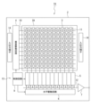
- FIG. 1 is a planar layout diagram illustrating a schematic configuration example of a solid-state imaging device according to a first embodiment of the present technology.
- 1 is a block diagram showing a configuration example of a solid-state imaging device according to a first embodiment of the present technology.
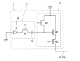
- 1 is an equivalent circuit diagram showing a configuration example of a pixel of a solid-state imaging device according to a first embodiment of the present technology.
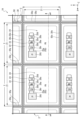
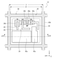
- 2 is a plan view illustrating a schematic planar pattern of an isolation region in a pixel array portion of the solid-state imaging device according to the first embodiment of the present technology.
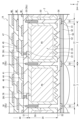
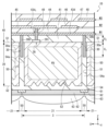
- FIG. 5 is a longitudinal sectional view showing a schematic longitudinal sectional structure taken along line a4-a4 in FIG. 4.
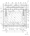
- FIG. 6 is a vertical cross-sectional view showing a part of FIG.
- FIG. 7 is a diagram for explaining the reflection of oblique light 71 on the side opposite to the multilayer wiring layer side (light incident surface side of the semiconductor layer) of the isolation region.
- FIG. 7 is a diagram for explaining the reflection of oblique light on the multilayer wiring layer side of the isolation region (the first surface side of the semiconductor layer) and the absorption of reflected light on the multilayer wiring layer side of the photoelectric conversion region (semiconductor layer).
- FIG. 7 is a diagram for explaining the embedding depth (embedding height) of the light shielding body 30 embedded in the isolation region 50.
- FIG. 2 is a plan view showing a diagonal direction of a photoelectric conversion region in a plan view.
- FIG. 1 is a plan view illustrating a first modified example of the first embodiment of the present technology.
- FIG. 11 is a longitudinal sectional view illustrating a modified example 2 of the first embodiment of the present technology.
- FIG. 11 is a longitudinal sectional view illustrating a third modified example of the first embodiment of the present technology.
- FIG. 13 is a longitudinal sectional view illustrating a fourth modified example of the first embodiment of the present technology.
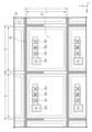
- FIG. 13 is a plan view illustrating a schematic planar pattern of an isolation region in a pixel array portion of a solid-state imaging device according to a second embodiment of the present technology.
- FIG. 13 is a longitudinal sectional view showing a schematic longitudinal sectional structure taken along line a12-a12 in FIG. 12.
- 13 is a plan view illustrating a schematic planar pattern of an isolation region in a pixel array portion of a solid-state imaging device according to a third embodiment of the present technology.
- FIG. 15 is a longitudinal sectional view showing a schematic longitudinal sectional structure taken along line a14-a14 in FIG. 14.
- FIG. 13 is a plan view illustrating a schematic planar pattern of an isolation region in a pixel array portion of a solid-state imaging device according to a fourth embodiment of the present technology.
- FIG. 17 is a longitudinal sectional view showing a schematic longitudinal sectional structure taken along line a16-a16 in FIG. 16.
- 13 is a plan view illustrating a schematic planar pattern of an isolation region in a pixel array portion of a solid-state imaging device according to a fifth embodiment of the present technology.
- FIG. 20 is a longitudinal sectional view showing a schematic longitudinal sectional structure taken along line a18-a18 in FIG. 13 is a longitudinal sectional view illustrating a schematic longitudinal sectional structure of a solid-state imaging device according to a sixth embodiment of the present technology.
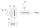
- FIG. FIG. 23 is a diagram showing a configuration example of an electronic device according to a seventh embodiment of the present technology.
- up and down and other directions in the following explanation are merely for the convenience of explanation and do not limit the technical ideas of this technology. For example, if an object is rotated 90 degrees and observed, up and down are converted into left and right and read, and of course, if it is rotated 180 degrees and observed, up and down are read inverted.
- the first and second directions that are mutually orthogonal in three directions (X direction, Y direction, Z direction) in space are respectively the X direction and the Y direction, which are mutually orthogonal in a two-dimensional plane of the semiconductor layer 20 described later, and the third direction that is orthogonal to each of the first and second directions is respectively the Z direction that runs along the thickness direction of the semiconductor layer 20.
- CMOS complementary metal oxide semiconductor
- the solid-state imaging device 1A is mainly composed of a semiconductor chip 2 that has a rectangular two-dimensional planar shape when viewed in a plan view.
- the solid-state imaging device 1A is mounted on the semiconductor chip 2, and the semiconductor chip 2 can be considered as the solid-state imaging device 1A.
- this solid-state imaging device 1A (101) takes in image light (incident light 106) from a subject via an optical lens 102, converts the amount of incident light 106 focused on the imaging surface into an electrical signal on a pixel-by-pixel basis, and outputs it as a pixel signal.
- the semiconductor chip 2 on which the solid-state imaging device 1A is mounted has a square pixel array section 2A provided in the center in a two-dimensional plane including mutually orthogonal X and Y directions, and a peripheral section 2B provided outside the pixel array section 2A so as to surround the pixel array section 2A.
- the semiconductor chip 2 is formed by dicing a semiconductor wafer including a semiconductor layer 20 described below into chip formation regions. Therefore, the configuration of the solid-state imaging device 1A described below is generally the same in the wafer state before the semiconductor wafer is diced. In other words, this technology can be applied in the state of a semiconductor chip and in the state of a semiconductor wafer.
- the pixel array section 2A is a light receiving surface that receives light collected by, for example, an optical lens (optical system) 102 shown in FIG. 21.
- a plurality of sensor pixels 3 are arranged in a matrix on a two-dimensional plane including the X direction and the Y direction.
- the sensor pixels 3 are repeatedly arranged in each of the X direction and the Y direction that are mutually orthogonal on the two-dimensional plane.
- a plurality of bonding pads 14 are arranged in the peripheral portion 2B.
- Each of the plurality of bonding pads 14 is arranged, for example, along each of the four sides of the semiconductor chip 2 in a two-dimensional plane.
- Each of the plurality of bonding pads 14 functions as an input/output terminal that electrically connects the semiconductor chip 2 to an external device.
- the semiconductor chip 2 includes a logic circuit 13 shown in Fig. 2.
- the logic circuit 13 includes a vertical drive circuit 4, a column signal processing circuit 5, a horizontal drive circuit 6, an output circuit 7, and a control circuit 8.
- the logic circuit 13 is configured of a CMOS (Complementary MOS) circuit having, as field effect transistors, for example, an n-channel conductivity type Metal Oxide Semiconductor Field Effect Transistor (MOSFET) and a p-channel conductivity type MOSFET.
- CMOS Complementary MOS
- the vertical drive circuit 4 is composed of, for example, a shift register.
- the vertical drive circuit 4 sequentially selects the desired pixel drive lines 10, supplies pulses to the selected pixel drive lines 10 for driving the sensor pixels 3, and drives each sensor pixel 3 row by row. That is, the vertical drive circuit 4 sequentially selects and scans each sensor pixel 3 in the pixel array section 2A vertically row by row, and supplies pixel signals from the sensor pixels 3 based on signal charges generated by the photoelectric conversion section (photoelectric conversion element) of each sensor pixel 3 according to the amount of light received to the column signal processing circuit 5 via the vertical signal line 11.
- the column signal processing circuit 5 is arranged, for example, for each column of sensor pixels 3, and performs signal processing such as noise removal for each pixel column on the signals output from one row of sensor pixels 3.
- the column signal processing circuit 5 performs signal processing such as CDS (Correlated Double Sampling) and AD (Analog-to-Digital) conversion to remove pixel-specific fixed pattern noise.
- the horizontal drive circuit 6 is composed of, for example, a shift register.
- the horizontal drive circuit 6 sequentially outputs horizontal scanning pulses to the column signal processing circuits 5, thereby selecting each of the column signal processing circuits 5 in turn, and causing each of the column signal processing circuits 5 to output a pixel signal that has been subjected to signal processing to the horizontal signal line 12.
- the output circuit 7 processes and outputs pixel signals sequentially supplied from each of the column signal processing circuits 5 through the horizontal signal line 12.
- the signal processing may include buffering, black level adjustment, column variation correction, various types of digital signal processing, etc.
- the control circuit 8 generates clock signals and control signals that serve as the basis for the operation of the vertical drive circuit 4, column signal processing circuit 5, horizontal drive circuit 6, etc., based on the vertical synchronization signal, horizontal synchronization signal, and master clock signal. The control circuit 8 then outputs the generated clock signals and control signals to the vertical drive circuit 4, column signal processing circuit 5, horizontal drive circuit 6, etc.
- each of the sensor pixels 3 includes a photoelectric conversion region 21 and a pixel circuit (readout circuit) 15.
- the photoelectric conversion region 21 includes a photoelectric conversion unit 24, a transfer transistor TR as a pixel transistor, and a floating diffusion region FD as a charge holding unit.
- the pixel circuit 15 is electrically connected to the floating diffusion region FD of the photoelectric conversion region 21.
- a circuit configuration is used in which one pixel circuit 15 is assigned to one sensor pixel 3, but the present invention is not limited to this first embodiment.
- a circuit configuration may be used in which one pixel circuit 15 is shared by multiple sensor pixels 3.
- a circuit configuration may be used in which one pixel circuit 15 is shared by one sensor pixel group (photoelectric conversion group) in which four sensor pixels 3 are arranged in a 2 ⁇ 2 arrangement, two in each of the X and Y directions, as one unit.
- a circuit configuration may be used in which one pixel circuit 15 is shared by one sensor pixel group (photoelectric conversion group) in which two sensor pixels 3 are arranged as one unit.
- a circuit configuration may be used in which one pixel circuit 15 is shared by one sensor pixel group (photoelectric conversion group) in which four or more sensor pixels 3 are arranged as one unit.
- the transfer transistor TR corresponds to a specific example of the "pixel transistor provided on the first surface side of the semiconductor layer" of the present technology
- the floating diffusion region FD corresponds to a specific example of the "charge holding portion" of the present technology.
- the photoelectric conversion unit 24 shown in FIG. 3 is composed of, for example, a pn junction type photodiode (PD) and generates a signal charge according to the amount of light received.
- the cathode side of the photoelectric conversion unit 24 is electrically connected to the source region of the transfer transistor TR, and the anode side is electrically connected to a reference potential line (for example, ground).
- the transfer transistor TR shown in FIG. 3 transfers the signal charge photoelectrically converted by the photoelectric conversion unit 24 to the floating diffusion region FD.
- the source region of the transfer transistor RT is electrically connected to the cathode side of the photoelectric conversion unit 24, and the drain region of the transfer transistor TR is electrically connected to the floating diffusion region FD.
- the gate electrode of the transfer transistor TR is electrically connected to the transfer transistor drive line of the pixel drive line 10 (see FIG. 2).
- the floating diffusion region FD shown in FIG. 3 temporarily holds (accumulates) the signal charge transferred from the photoelectric conversion unit 24 via the transfer transistor TR.
- the pixel circuit 15 shown in FIG. 3 reads out the signal charge held in the floating diffusion region FD and outputs a pixel signal based on the read out signal charge.
- the pixel circuit 15 includes, but is not limited to, an amplification transistor AMP, a selection transistor SEL, and a reset transistor RST as pixel transistors.
- Each of these pixel transistors (AMP, SEL, RST) and the transfer transistor TR described above is configured as a field effect transistor, for example, a MOSFET having a gate insulating film made of a silicon oxide (SiO 2 ) film, a gate electrode, and a pair of main electrode regions functioning as a source region and a drain region.
- these transistors may be MISFETs (Metal Insulator Semiconductor FETs) whose gate insulating film is made of a silicon nitride (Si 3 N 4 ) film or a laminated film such as a silicon nitride film and a silicon oxide film.
- MISFETs Metal Insulator Semiconductor FETs
- each of the amplification transistor AMP, the selection transistor SEL, and the reset transistor RST corresponds to a specific example of a "pixel transistor" of the present technology.
- the source region of the amplification transistor AMP is electrically connected to the drain region of the selection transistor SEL, and the drain region is electrically connected to the power supply line Vdd and the drain region of the reset transistor RST.
- the gate electrode of the amplification transistor AMP is electrically connected to the floating diffusion region FD and the source region of the reset transistor RST.
- the source of the selection transistor SEL is electrically connected to the vertical signal line 11 (VSL), and the drain region is electrically connected to the source region of the amplification transistor AMP.
- the gate electrode of the selection transistor SEL is electrically connected to the selection transistor drive line of the pixel drive line 10 shown in FIG. 2.
- the source region of the reset transistor RST is electrically connected to the floating diffusion region FD and the gate electrode of the amplifier transistor AMP, and the drain region is electrically connected to the power supply line Vdd and the drain region of the amplifier transistor AMP.
- the gate electrode of the reset transistor RST is electrically connected to the reset transistor drive line of the pixel drive line 10 shown in FIG. 2.
- the transfer transistor TR transfers the signal charge generated in the photoelectric conversion unit 24 to the floating diffusion region FD.
- the selection transistor SEL controls the output timing of the pixel signal from the pixel circuit 15.
- the amplification transistor AMP shown in FIG. 3 generates a pixel signal whose voltage corresponds to the level of the signal charge held in the floating diffusion region FD.
- the amplification transistor AMP constitutes a source-follower type amplifier, and outputs a pixel signal whose voltage corresponds to the level of the signal charge generated in the photoelectric conversion unit 24.
- the selection transistor SEL is turned on, the amplification transistor AMP amplifies the potential of the floating diffusion region FD, and outputs a voltage corresponding to that potential to the column signal processing circuit 5 via the vertical signal line 11 (VSL).
- the signal charge generated in the photoelectric conversion unit 24 of the sensor pixel 3 is held (accumulated) in the floating diffusion region FD via the transfer transistor TR of the sensor pixel 3.
- the signal charge held in the floating diffusion region FD is read out by the pixel circuit 15 and applied to the gate electrode of the amplification transistor AMP of the pixel circuit 15.
- a horizontal line selection control signal is provided to the gate electrode of the selection transistor SEL of the pixel circuit 15 from the vertical shift register.
- the selection transistor SEL becomes conductive, and a current corresponding to the potential of the floating diffusion region FD amplified by the amplification transistor AMP flows in the vertical signal line 11. Also, by setting the reset control signal applied to the gate electrode of the reset transistor RST of the pixel circuit 15 to a high (H) level, the reset transistor RST becomes conductive, and the signal charge accumulated in the floating diffusion region FD is reset.
- the selection transistor SEL may be omitted if necessary.
- the source region of the amplification transistor AMP is electrically connected to the vertical signal line 11 (VSL).
- a switching transistor may also be provided between the reset transistor RST and the gate electrode of the floating diffusion region FD and the amplifier transistor AMP.
- the switching transistor controls charge retention by the floating diffusion region FD and adjusts the voltage multiplication factor according to the potential amplified by the amplifier transistor AMP.
- the switching transistor is also used to switch the conversion efficiency.
- the FD capacitance C of the charge holding section needs to be large so that the voltage V when converted to voltage by the amplification transistor AMP does not become too large (in other words, so that it becomes small).
- the switching transistor when the switching transistor is turned on, the gate capacitance of the switching transistor increases, so the overall FD capacitance C becomes large.
- the switching transistor when the switching transistor is turned off, the overall FD capacitance C becomes small. In this way, by switching the switching transistor on/off, the FD capacitance C can be made variable and the conversion efficiency can be switched.
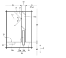
- FIG. 4 is a plan view illustrating a schematic planar pattern of an isolation region in a pixel array portion of the solid-state imaging device according to the first embodiment of the present technology.
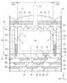
- FIG. 5 is a vertical cross-sectional view that typically shows a vertical cross-sectional structure taken along line a4-a4 in FIG.
- FIG. 6 is a vertical cross-sectional view showing a part of FIG. 4 is a plan view seen from the opposite side to the paper surface of FIG. 5 and 6 omit illustration of layers above an interlayer insulating film 44 of a multi-layer wiring layer 40, which will be described later.
- the semiconductor chip 2 comprises a semiconductor layer 20 having a first surface portion S1 and a second surface portion S2 located opposite each other in the thickness direction (Z direction), an isolation region 50 provided in the semiconductor layer 20, and a plurality of photoelectric conversion regions 21 provided in the semiconductor layer 20 and partitioned by the isolation region 50.
- the semiconductor chip 2 further includes a photoelectric conversion section 24 that is provided in each of the multiple photoelectric conversion regions 21 and photoelectrically converts light incident (penetrating) from the second surface S2 side of the semiconductor layer 20, and a light shield 30 and a multilayer wiring layer 48 that are provided on the first surface S1 side of the semiconductor layer 20.
- the semiconductor chip 2 further includes an insulating film 54 provided on the second surface S2 side of the semiconductor layer 20, and a light-shielding film 61, a color filter 62, and a microlens (on-chip lens) 63 provided in this order from the insulating film 54 side on the side opposite the semiconductor layer 20 side of the insulating film 54.
- the semiconductor layer 20 includes an isolation region 50 extending in the thickness direction (Z direction) of the semiconductor layer 20, and a plurality of photoelectric conversion regions 21 partitioned by the isolation region 50.
- Each of the plurality of photoelectric conversion regions 21 is provided for each sensor pixel 3, and is adjacent to one another via the isolation region 50 in a plan view. That is, the solid-state imaging device 1A of the first embodiment includes a plurality of photoelectric conversion regions 21 provided in the semiconductor layer 20 adjacent to one another via the isolation region 50 extending in the thickness direction (Z direction) of the semiconductor layer 20.
- a Si substrate, a SiGe substrate, an InGaAs substrate, or the like can be used as the semiconductor layer 20.
- a p-type semiconductor substrate made of single crystal silicon, for example, is used as the semiconductor layer 20.
- the first surface S1 of the semiconductor layer 20 is sometimes called the element formation surface or main surface
- the second surface S2 is sometimes called the light incident surface or back surface.
- the solid-state imaging device 1A of this first embodiment is a back-illuminated type in which light incident from the second surface (light incident surface, back surface) S2 of the semiconductor layer 20 is photoelectrically converted by a photoelectric conversion unit 24 provided in the photoelectric conversion region 21 of the semiconductor layer 20.
- a planar view refers to a view from a direction along the thickness direction (Z direction) of the semiconductor layer 20.
- a cross-sectional view refers to a view of a vertical section along the thickness direction (Z direction) of the semiconductor layer 20 from a direction (X direction or Y direction) perpendicular to the thickness direction (Z direction) of the semiconductor layer 20.
- the photoelectric conversion region 21 can also be called a photoelectric conversion cell.
- each of the multiple photoelectric conversion regions (photoelectric conversion cells) 21 includes a p-type well region 22 provided in the semiconductor layer 20, an n-type semiconductor region 23 provided in the p-type well region 22, a photoelectric conversion section 24, and a diffraction scattering section 52. Also, as shown in Fig. 4, each photoelectric conversion region 21 further includes the above-mentioned pixel transistors (AMP, SEL, RST, TR) and a floating diffusion region FD.
- the p-type well region 22 is provided widely across the first surface portion S1 side and the second surface portion S2 side of the semiconductor layer 20.
- the p-type well region 22 is composed of, for example, a p-type semiconductor region.
- the n-type semiconductor region 23 is provided in the p-type well region 22 across the first surface S1 side and the second surface S2 side of the semiconductor layer 20, while being spaced apart from each of the first surface S1 and the second surface S2 of the semiconductor layer 20 and the isolation region 50. That is, the upper surface of the n-type semiconductor region 23 on the first surface S1 side of the semiconductor layer 20, the lower surface of the n-type semiconductor region 23 on the second surface S2 side of the semiconductor layer 20, and the side surface of the n-type semiconductor region 23 on the isolation region 50 side are each surrounded by the p-type well region 22.
- the p-type well region 22 is provided between the first surface S1 of the semiconductor layer 20 and the upper surface of the n-type semiconductor region 23, and between the second surface S2 of the semiconductor layer 20 and the lower surface of the n-type semiconductor region 23, overlapping with the n-type semiconductor region 23.
- a p-type well region 22 is provided between the isolation region 50 and the n-type semiconductor region 23, and extends along the thickness direction (Z direction) of the semiconductor layer 20.
- the transfer transistor TR shown in Figure 4 includes a gate electrode 26t provided on the first surface portion S1 side of the semiconductor layer 20 via a gate insulating film, a photoelectric conversion portion 24 that mainly functions as a source region, and a main electrode region 25a that is provided in the surface portion (upper portion) on the first surface portion S1 side of the semiconductor layer 20 and mainly functions as a drain region.
- the reset transistor RST shown in FIG. 4 includes, although not shown in detail, a gate electrode 26r provided on the first surface portion S1 side of the semiconductor layer 20 via a gate insulating film, a main electrode region 25a that mainly functions as a source region, and a main electrode region 25b that is provided in the surface layer portion (upper portion) on the first surface portion S1 side of the semiconductor layer 20 and mainly functions as a drain region. That is, the reset transistor RST and the transfer transistor TR share their respective main electrode regions 25a and are connected in series.
- the amplification transistor AMP shown in FIG. 4 includes, although not shown in detail, a gate electrode 26a provided on the first surface S1 side of the semiconductor layer 20 via a gate insulating film, a main electrode region 25c provided on the surface layer (upper portion) of the first surface S1 side of the semiconductor layer 20, and mainly functions as a source region, and a main electrode region 25b mainly functions as a drain region. That is, the amplification transistor AMP and the reset transistor RST share the main electrode region 25b and are connected in series.
- the selection transistor SEL shown in FIG. 4 includes, although not shown in detail, a gate electrode 26s provided on the first surface S1 side of the semiconductor layer 20 via a gate insulating film, a main electrode region 25d provided on the surface portion (upper portion) of the first surface S1 side of the semiconductor layer 20, and mainly functions as a source region, and a main electrode region 25c mainly functions as a drain region. That is, the selection transistor SEL and the amplification transistor AMP share the main electrode region 25c and are connected in series.
- the gate insulating film is composed of, for example, a silicon oxide film.
- the gate electrodes 26t, 26r, 26a, and 26s are composed of, for example, a polycrystalline silicon film into which an impurity that reduces the resistance value is introduced.
- the main electrode regions 25a, 25b, 25c, and 25d are composed of, for example, an n-type semiconductor region provided in the p-type semiconductor region 22 of the photoelectric conversion region 21.
- the pixel transistors are not shown in detail, but are provided for each photoelectric conversion region 21 on the surface layer on the first surface portion S1 side of the semiconductor layer 20, and each gate electrode (26t, 26r, 26a, 26s) is provided on the first surface portion S1 side of the semiconductor layer 20.
- the floating diffusion region FD shown in FIG. 4 is not shown in detail, but is provided in the surface layer (upper part) on the first surface portion S1 side of the semiconductor layer 20. As shown in FIG. 4, the floating diffusion region FD is shared with the main electrode region 25a. In other words, the floating diffusion region FD is composed of an n-type semiconductor region provided in the p-type semiconductor region 22 of the photoelectric conversion region 21.
- each of the pixel transistors (TR, AMP, SEL, RST) is disposed at a position different from the position of the line a4-a4 in FIG. 4 in a plan view, but in FIG. 5 and FIG. 6, the gate electrode 26t of the transfer transistor TR is illustrated as an example of the pixel transistors TR, AMP, SEL, RST.
- the separation region 50 individually separates each of the multiple photoelectric conversion regions 21.
- the separation region 50 includes a first portion 50x extending in the X direction in a plan view and a second portion 50y extending in the Y direction.
- the first portion 50x and the second portion 50y are perpendicular to each other.
- the first portions 50x are repeatedly arranged in the Y direction at a predetermined interval.
- the second portions 50y are repeatedly arranged in the X direction at a predetermined interval. That is, the separation region 50 has a lattice-like planar pattern in a planar view.
- Each of the multiple photoelectric conversion regions 21 is partitioned at both ends in the X direction by two adjacent second portions 50y of the separation region 50, and at both ends in the Y direction by two adjacent first portions 50x of the separation region 50.
- the separation region 50 extends in the thickness direction (Z direction) of the semiconductor layer 20 in a vertical cross-sectional view, and electrically and optically separates adjacent photoelectric conversion regions 21.
- the separation region 50 extends across the first surface portion S1 side and the second surface portion S2 side of the semiconductor layer 20 in a vertical cross-sectional view.
- the separation region 50 reaches, for example, both the first surface portion S1 and the second surface portion S2 of the semiconductor layer 20, although this is not limited thereto.
- the separation region 50 includes a recessed portion 51 that extends in the depth direction (Z direction) of the semiconductor layer 20, and an insulating film 54a that is provided in the recessed portion 51 across the second surface portion S2 side and the first surface portion S1 side of the semiconductor layer 20 and serves as a light reflector having a lower refractive index than the semiconductor layer 20.
- Air can also be used as a dielectric material having a lower refractive index than the semiconductor layer 20.
- the separation region 50 includes a cavity filled with air.
- the recessed portion 51 of the first embodiment corresponds to a specific example of a "recessed portion of a semiconductor layer" in the present technology
- the insulating film 54a of the first embodiment corresponds to a specific example of a "dielectric" in the present technology.
- the insulating film 54a is provided within the recessed portion 51 of the semiconductor layer 20, from the second surface portion S2 side to the first surface portion S1 side of the semiconductor layer 20.
- the insulating film 54a within the recessed portion 51 is integrated with the insulating film 54 provided on the second surface portion S2 side of the semiconductor layer 20.
- the insulating films 54 and 54a may be, for example, silicon oxide films. Silicon oxide films have a lower refractive index than semiconductor materials such as Si, SiGe, and InGaAs.
- the insulating film 54a in the recessed portion 51 which will be described in detail later, mainly functions as a light reflector that reflects oblique light 71 irradiated from the predetermined photoelectric conversion region 21 side to the interface If (see FIG. 7) between the photoelectric conversion region 21 and the separation region 50, and returns it to the predetermined photoelectric conversion region 21.
- the insulating film 54a on the first surface S1 side of the semiconductor layer 20 covers the entire second surface S2 side of the semiconductor layer 20 in the pixel array section 2A so that the second surface S2 (light incident surface) side of the semiconductor layer 20 is a flat surface without any irregularities.
- the multilayer wiring layer (wiring layer stack) 40 is provided on the first surface S1 side opposite to the light incident surface side (second surface S2 side) of the semiconductor layer 20.
- the multilayer wiring layer 40 has a stacked structure including, but not limited to, an interlayer insulating film 41, a first wiring layer M1, an interlayer insulating film 44, a second wiring layer M2, an interlayer insulating film 46, a third wiring layer M3, an interlayer insulating film 48, and the like, which are stacked in order from the first surface S1 side of the semiconductor layer 20.
- the interlayer insulating film 41 is provided on the first surface portion S1 side of the semiconductor layer 20 so as to cover the gate electrodes of the pixel transistors (AMP, SEL, RST, TR). In FIG. 6, only the gate electrode 26t of the transfer transistor TR is shown.
- a first-layer wiring layer M1 is provided on the interlayer insulating film 41, and this first-layer wiring layer M1 is covered by the upper interlayer insulating film 44.
- a second-layer wiring layer M2 is provided on the interlayer insulating film 44, and this second-layer wiring layer M2 is covered by the upper interlayer insulating film 46.
- a third-layer wiring layer M3 is provided on the interlayer insulating film 46, and this third-layer wiring layer M3 is covered by the upper interlayer insulating film 48.
- FIG. 5 and 6 respectively show wiring 43 formed on the first wiring layer M1, wiring 45 formed on the second wiring layer M2, and wiring 47 formed on the third wiring layer M3.
- Each of the first to third wiring layers M1 to M3 is made of a metal film such as copper (Cu) or an alloy mainly made of Cu.
- Each of the interlayer insulating films 41 to 48 is made of a single layer film of any one of a silicon oxide film, a silicon nitride (Si 3 N 4 ) film, and a silicon carbonitride (SiCN) film, or a laminated film of any two or more of these films.
- the diffraction scattering section 52 has a configuration in which periodic irregularities are provided on the interface on the light incident surface side (second surface portion S2 side) of the semiconductor layer 20.
- the diffraction scattering section 52 is provided so as to overlap the photoelectric conversion section 24 for each photoelectric conversion region 21 in a plan view.
- the irregularities of the diffraction scattering section 52 are covered with an insulating film 54 provided on the first surface portion S1 side of the semiconductor layer 20.
- the unevenness of the diffraction scattering section 52 acts as a diffraction grating, and higher-order components are diffracted in an oblique direction, making it possible to lengthen the optical path length within the photoelectric conversion section 24 and improving the sensitivity of near-infrared light components in particular.
- the diffraction scattering section 52 can be a quadrangular pyramid formed by wet etching the Si(111) surface using alkaline ionized water (AKW).
- the diffraction scattering section 52 may be formed by dry etching. Furthermore, by making the shape such that the cross-sectional area changes in the depth direction, reflection is suppressed and the sensitivity is slightly improved.
- the light-shielding film 61 is provided on the side opposite to the semiconductor layer 20 side of the insulating film 54.
- the light-shielding film 61 has a lattice-like planar pattern in plan view that opens the light-receiving surface side of each of the multiple photoelectric conversion regions 21 so that light incident (penetrating) into a specific photoelectric conversion region 21 does not leak into an adjacent photoelectric conversion region 21.
- the light-shielding film 61 is configured with the same lattice-like planar pattern as the separation region 50, and is disposed at a position overlapping the separation region 50 in plan view.
- a tungsten (W) film having light-shielding properties is used as the light-shielding film 61.
- the color filters 62 are provided for each photoelectric conversion region 21 (sensor pixel 3) on the side (light incident surface side) opposite to the semiconductor layer 20 side of the light shielding film 61.
- the color filters 62 separate the incident light from the light incident surface side of the semiconductor chip 2 into colors.
- the color filters 62 include a first color filter of red (R), a second color filter of green (G), and a third color filter of blue (B).
- R red
- G second color filter of green
- B third color filter of blue
- the color filters 62 of three colors, R, G, and B are provided.
- the microlenses 63 are provided for each photoelectric conversion region 21 (sensor pixel 3) on the side of the color filter 62 opposite the light-shielding film 61 (light incident side).
- the microlenses 63 focus the irradiated light and allow the focused light to efficiently enter the photoelectric conversion region 21.
- the light shield 30 is provided on the first surface S1 side of the semiconductor layer 20.
- the light shield 30 is provided across the isolation region 50 and the multi-layer wiring layer 40 in the thickness direction (Z direction) of the semiconductor layer 20, and is made of a metal film having a higher extinction coefficient than the semiconductor layer 20.
- a tungsten (W) film having light shielding properties is used as the light shield 30.
- the tungsten film has a higher refractive index than semiconductor materials such as Si, SiGe, and InGaAs.
- the light shield 30 has a buried portion (first portion) 31a located within the isolation region 50 in the thickness direction (Z direction) of the semiconductor layer 20 and surrounded by the insulating film 54a of the isolation region 50, and a protruding portion (second portion) 30b protruding from the buried portion 31a into the wiring layer 40 and surrounded by the interlayer insulating film 41 of the multilayer wiring layer 40.
- the buried portion 31a of the light shield 30 is adjacent to the photoelectric conversion region 21 of the semiconductor layer 20 via the insulating film 54a of the isolation region 50 in a direction perpendicular to the thickness direction (Z direction) of the semiconductor layer 20.
- the light shield 30 has a lattice-like planar pattern in plan view that opens the light receiving surface side of each of the multiple photoelectric conversion regions 21, as shown in FIG. 4, so that light that is incident from the light incident surface side (second surface S2 side) of the semiconductor layer 20 and transmitted through a specified photoelectric conversion region 21 is not reflected by the wiring of the multilayer wiring layer 40 or the gate electrode of the pixel transistor and does not enter an adjacent photoelectric conversion region 21 different from the specified photoelectric conversion region 21 as unwanted light.
- the light shield 30 has a lattice-like planar pattern similar to the separation region 50 of the lattice-like planar pattern, and overlaps with the separation region 50 in plan view.
- the light shield 30 includes a first portion 3x extending in the X direction in a plan view and a second portion 30y extending in the Y direction.
- the first portion 30x and the second portion 30y are perpendicular to each other.
- the first portions 30x are repeatedly arranged in the Y direction with the same arrangement pitch as the first portions 50x of the separation region 50
- the second portions 30y are repeatedly arranged in the X direction with the same arrangement pitch as the second portions 50y of the separation region 50.
- the first portion 30x of the light shield 30 overlaps with the first portion 50x of the separation region 50 in a plan view
- the second portion 30y of the light shield 30 overlaps with the second portion 50y of the separation region 50 in a plan view.
- the light shields 30 corresponding to multiple photoelectric conversion regions 21 have a lattice-like planar pattern, while the light shields 30 corresponding to one photoelectric conversion region 21 have an annular planar pattern that surrounds the periphery of one photoelectric conversion region 21.
- the light shields 30 of this first embodiment continuously surround the periphery of one photoelectric conversion region 21 in an annular (ring-like) shape in a planar view.
- FIG. 7 is a vertical cross-sectional view that typically illustrates oblique light 71 in the photoelectric conversion region 21 and light reflected on the multilayer wiring layer 40 side of the photoelectric conversion region 21 (semiconductor layer 20).
- FIG. 8A is a diagram for explaining the reflection of oblique light 71 on the side of isolation region 50 opposite to multilayer wiring layer 40 side (light incident surface side of semiconductor layer 20) in FIG.
- FIG. 8B is a diagram for explaining the reflection of oblique light 71 on the multilayer wiring layer 40 side (the first surface S1 side of the semiconductor layer 20) of the isolation region 50 in FIG. 7, and the absorption of the reflected light on the multilayer wiring layer 40 side of the semiconductor layer 20.
- FIG. 8C is a diagram for explaining the embedding depth (embedding height) of the light shielding body 30 embedded in the isolation region 50 in FIG.
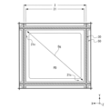
- FIG. 8D is a plan view showing the diagonal direction of the photoelectric conversion region in a plan view. It should be noted that FIG. 7 is upside down compared to FIG.
- incident light 70 passes through the microlens 63, the color filter 62, the insulating film 54, the diffractive scattering portion 52, etc., and enters the photoelectric conversion region 21 from the second surface portion S2 side (light incident surface side) of the semiconductor layer 20.
- oblique light 71 is generated from the incident light 70 due to collection by the microlens 63 and scattering by the diffractive scattering portion 52.
- oblique light 71 generated in the photoelectric conversion region 21 is irradiated (hits) on the interface If between the photoelectric conversion region 21 and the insulating film 54a of the isolation region 50 on the light incident surface side of the semiconductor layer 20 (the side opposite to the multilayer wiring layer 40 side of the semiconductor layer 20).
- the refractive index of the photoelectric conversion region 21 is n2
- the refractive index of the insulating film (dielectric) 54a of the isolation region 50 is n1
- the angle formed at the interface If between a virtual line La perpendicular to the thickness direction (Z direction) of the photoelectric conversion region 21 (semiconductor layer 20) and oblique light 71 irradiated to the interface If is defined as ⁇ ,
- n2>n1 If the oblique light 71 satisfies Sin ⁇ >n1/n2, then Oblique light 71 irradiated onto the interface If between the photoelectric conversion region 21 and the insulating film 54 of the separation region 50 is totally reflected toward the photoelectric conversion region 21 and returns to the photoelectric conversion region 21 .
- the generated oblique light 71 is irradiated (hits) on the interface If between the photoelectric conversion region 21 and the insulating film 54a of the isolation region 50 on the multilayer wiring layer 40 side of the photoelectric conversion region 21 (the multilayer wiring layer 40 side of the semiconductor layer 20) as shown in FIG. 8B. If "Sin ⁇ >n1/n2" when "n2>n1", the oblique light 71 irradiated on this interface If is also totally reflected towards the photoelectric conversion region 21 and returns to the photoelectric conversion region 21.
- the photoelectric conversion region 21 is silicon
- the insulating film 54 of the separation region 50 is silicon oxide
- the refractive index of silicon oxide is lower than that of silicon, so in this case, "n2>n1", and for light with a wavelength of 940 nm, when " ⁇ >19.5°", "Sin ⁇ >n1/n2" is satisfied.
- an insulating film 54a with a refractive index (n1) lower than the refractive index (n2) of the semiconductor layer 20 as the light reflector contained in the separation region 50, the oblique light 71 irradiated to the interface If between the photoelectric conversion region 21 and the insulating film 54 of the separation region 50 is totally reflected from the second surface S2 side (light incident surface side) of the semiconductor layer 20 to the first surface S1 side (multilayer wiring layer 40 side) toward the photoelectric conversion region 21 when " ⁇ >19.5°" is satisfied, and returns to the photoelectric conversion region 21, so that a decrease in sensitivity can be suppressed.
- n1 refractive index
- the refractive index of air is also lower than that of silicon, so when the refractive index n1 is air, "Sin ⁇ >n2/n1" is satisfied when " ⁇ >13.8°” for light with a wavelength of 940 nm. Therefore, even when air is used as the light reflector contained in the separation region 50, the oblique light 71 irradiated to the interface If between the photoelectric conversion region 21 and the insulating film 54a of the separation region 50 is totally reflected from the second surface S2 side (light incident surface side) of the semiconductor layer 20 to the first surface S1 side (multilayer wiring layer 40 side) toward the photoelectric conversion region 21 when " ⁇ >13.8°” is satisfied, and returns to the photoelectric conversion region 21, thereby suppressing a decrease in sensitivity.
- silicon has a refractive index (n2) of, for example, about 3.62
- silicon oxide has a refractive index (n1) of, for example, about 1.45
- air has a refractive index (n1) of, for example, about 1.00
- silicon has a refractive index (n2) of, for example, about 4.08
- silicon oxide has a refractive index (n1) of, for example, about 1.46
- air has a refractive index (n1) of, for example, about 1.00.
- n2>n1 is satisfied.
- ⁇ Shielding reflected light> Next, a description will be given of the blocking of reflected light by the light blocking body 30.
- a gate reflected light 72 reflected by the gate electrode 26t of the transfer transistor TR will be described as an example of the reflected light reflected on the multilayer wiring layer 40 side of the semiconductor layer 20.
- oblique light 71 generated in the photoelectric conversion region 21 is reflected by the gate electrode 26t of the transfer transistor TR provided on the first surface S1 side of the semiconductor layer 20. Then, gate reflected light 72 reflected by the gate electrode 26t passes through the predetermined photoelectric conversion region 21 again and is irradiated onto the interface If.
- the refractive index of the photoelectric conversion region 21 semiconductor layer 20
- the extinction coefficient is k2.
- the refractive index of the insulating film (dielectric) 54a of the isolation region 50 is n1, and the extinction coefficient is k1.
- the extinction coefficient of the light blocking body 30 is k3,
- the angle formed at the interface If between a virtual line Lb perpendicular to the thickness direction (Z direction) of the semiconductor layer 20 and the gate reflected light 72 irradiated to the interface If is defined as ⁇ 1, When n1>n2, k3>k1, and k3>k2,
- the gate reflected light 72 of Sin ⁇ 1 ⁇ n2/n1 is transmitted through the insulating film 54a of the isolation region 50 and is irradiated (impinges) on the buried portion 30a of the light shield 30.
- the gate reflected light 72 irradiated on the buried portion 30a is absorbed (shielded) by this buried portion 30a.
- oblique light 71 generated in the photoelectric conversion region 21 is reflected by the gate electrode 26t of the transfer transistor TR, and the gate reflected light 72 reflected by this gate electrode 26t passes through the specified photoelectric conversion region 21 again, and then passes through the insulating film 54a of the separation region 50 to be irradiated onto the buried portion 30a of the light shield 30, where it is absorbed (blocked) by this buried portion 30a.
- the phenomenon in which the gate reflected light 72 reflected by this gate electrode 26t enters (penetrates) as unwanted light into an adjacent photoelectric conversion region 21 (21a) different from the specified photoelectric conversion region 21 can be suppressed by the embedded portion 30a of the light shield 30. This makes it possible to suppress color mixing.
- the light shield 30 is preferably made of a material with a high extinction coefficient k for the wavelength of light being used.
- the light shield 30 is made of, for example, a tungsten (W) film with a high extinction coefficient k for visible light and near-infrared light.
- the refractive index of air is lower than that of silicon, even when air is used as the light reflector contained in the separation region 50, the phenomenon in which the gate reflected light 72 reflected by the gate electrode 26t is incident as unwanted light on an adjacent photoelectric conversion region 21 (21a) different from the specified photoelectric conversion region 21 can be suppressed by the buried portion 30a of the light shield 30. This makes it possible to suppress color mixing.
- FIG. 8C and 8D The depth X1 of the embedded portion 30a of the light shield 30 is the depth from the first surface S1 of the semiconductor layer 20 toward the semiconductor layer 20.
- the height X2 of the protruding portion 30b of the light shield 30 is the height from the first surface S1 of the semiconductor layer 20 toward the multilayer wiring layer 40.
- the depth of the embedded portion 30a of the light shielding body 30 is X1 .
- the length from the light shield 30 to the starting point P1 of the gate reflected light 72 is defined as Y1 .
- the depth X1 of the embedded portion 30a of the light blocking body 30 is determined by " X1 > Y1 ⁇ tan ⁇ 0 ". Then, referring to FIG. 8D , the maximum value of Y1 is the length in a diagonal direction Dg connecting two corners 21c located on opposite sides of the photoelectric conversion region 21 in a plan view, and therefore the depth X1 of the embedded portion 30a of the light shielding body 30 satisfies the following conditions 1 and 2.
- Condition 1 Depth of X1 > Y1 ⁇ tan 19.5° or more (when n1 is silicon oxide)
- Condition 2 Depth of X1 > Y1 ⁇ tan 13.8° or more (when n1 is air)
- the insulating film 54a having a refractive index (n1) lower than the refractive index (n2) of the semiconductor layer 20 is used as the dielectric contained in the isolation region 50, by setting the depth X1 of the embedded portion 30a of the light shield 30 as condition 1, the gate reflected light 72 which is reflected by the gate electrode 26t and transmitted again through the predetermined photoelectric conversion region 21 and further transmitted through the insulating film 54a in the isolation region 50 can be absorbed and blocked by the embedded portion 30a of the light shield 30.
- the gate reflected light 72 which is reflected by the gate electrode 26t, transmitted again through the predetermined photoelectric conversion region 21, and further transmitted through the insulating film 54a in the separation region 50 can be absorbed and blocked by the embedded portion 30a of the light shield 30.
- the embedded portion 30a of the light shield 30 can suppress the phenomenon in which gate reflected light 72 reflected by the gate electrode 26t located on the multilayer wiring layer 40 side of the specified photoelectric conversion region 21 in a plan view is incident as unwanted light on an adjacent photoelectric conversion region 21 (21a) different from the specified photoelectric conversion region 21, thereby suppressing color mixing.
- the reflected light of the oblique light 71 reflected on the multilayer wiring layer 40 side of the photoelectric conversion region 21 also includes wiring reflected light reflected by the wiring of the multilayer wiring layer 40.
- the depth X1 of the embedded portion 30a of the light shield 30 to the above-mentioned condition 1 and condition 2
- the phenomenon in which the wiring reflected light reflected by the wiring located on the multilayer wiring layer 40 side of a predetermined photoelectric conversion region 21 in a plan view is incident as unnecessary light on an adjacent photoelectric conversion region 21 (21a) different from the predetermined photoelectric conversion region 21 can be suppressed by the embedded portion 30a of the light shield 30, and color mixing can be suppressed.
- the light shield 30 of the first embodiment has a protruding portion 40b protruding from the buried portion 30a toward the multilayer wiring layer 40. Therefore, the protruding portion 30b of the light shield 30 can also block the wiring reflected light that is reflected by the wiring of the multilayer wiring layer 40 that overlaps with the predetermined photoelectric conversion region 21 in a plan view, passes through the multilayer wiring layer 40 again, and enters an adjacent photoelectric conversion region 21 (21a) different from the predetermined photoelectric conversion region 21. This makes it possible to further suppress color mixing.
- the effect of suppressing color mixing caused by wiring reflected light is proportional to the height X2 of the protruding portion 30b of the light shield 30.
- the solid-state imaging device 1A includes the isolation region 50 and the light shielding body 30.
- the separation region 50 is provided in the recessed portion 51 of the semiconductor layer 20 across the first face portion S1 side and the second face portion S2 side of the semiconductor layer 20, and includes an insulating film 54a having a refractive index (n1) lower than the refractive index (n2) of the semiconductor layer 20.
- the oblique light 71 irradiated to the interface portion If between the photoelectric conversion region 21 and the insulating film 54 of the separation region 50 is totally reflected toward the photoelectric conversion region 21 across the second face portion S2 side (light incident surface side) of the semiconductor layer 20 to the first face portion S1 side (multilayer wiring layer 40 side), thereby suppressing a decrease in sensitivity.
- the light shield 30 is provided across the isolation region 50 and the multi-layer wiring layer 40, and has an extinction coefficient (k3) higher than the extinction coefficient (k2) of the semiconductor layer 20.
- the embedded portion 30a of the light shield 30 can suppress the phenomenon in which the gate reflected light 72 reflected by the gate electrode 26t overlapping the specified photoelectric conversion region 21 in a planar view as reflected light reflected on the multi-layer wiring layer 40 side of the specified photoelectric conversion region 21 enters (penetrates) as unwanted light into an adjacent photoelectric conversion region 21 (21a) different from the specified photoelectric conversion region 21, thereby suppressing color mixing.
- the phenomenon in which light reflected from the wiring of the multilayer wiring layer 40 that overlaps the specified photoelectric conversion region 21 in a planar view as reflected light is incident as unwanted light on an adjacent photoelectric conversion region 21 (21a) different from the specified photoelectric conversion region 21 can be suppressed by the embedded portion 30a and protruding portion 30b of the light shielding body 30, thereby suppressing color mixing.
- the solid-state imaging device 1A according to the first embodiment can suppress the decrease in sensitivity that causes deterioration in image quality, and can also suppress color mixing that causes deterioration in image quality. Therefore, the solid-state imaging device 1A according to the first embodiment can achieve high image quality.
- the light shield 30 surrounds the photoelectric conversion region 21 in a continuous ring shape in a plan view. This allows the light shield 30 to absorb gate reflected light 72 reflected by the gate electrode 26t of the transfer transistor TR and wiring reflected light reflected by the wiring of the multilayer wiring layer 40 over the entire circumference of the photoelectric conversion region 21, thereby further enhancing the effect of suppressing color mixing.
- the gate reflected light 72 reflected by the gate electrode 26t of the transfer transistor TR has been described as an example of gate reflected light formed when the oblique light 71 is reflected on the multilayer wiring layer 40 side of the photoelectric conversion region 21, but is not limited to this gate reflected light 72.
- other gate reflected light includes gate reflected light reflected by the gate electrodes (26r, 26a, 26s) of the reset transistor RST, the amplification transistor AMP, and the selection transistor SEL included in the pixel circuit 15. These gate reflected light beams can also be blocked by the embedded portion 30a of the light shield 30.
- the planar shape of the light shielding body 30 corresponding to one photoelectric conversion region 21 is described as a planar shape that continuously surrounds the periphery of the photoelectric conversion region 21 in a ring shape, but the planar shape of the light shielding body 30 is not limited to the above-described first embodiment.
- the light shields 30 corresponding to one photoelectric conversion region 21 may have a planar shape that is dotted in an annular shape surrounding the periphery of the photoelectric conversion region 21 in a plan view.
- the light shield 30 corresponding to one photoelectric conversion region 21 may have a planar shape surrounding part of the periphery of the pixel transistors (TR, RST, AMP, SEL). In this case, when a plurality of pixel transistors are grouped, the light shield 30 has a planar shape surrounding part of the periphery of the group.
- the height X2 of the protruding portion 30b of the light shield 30 (the height protruding upward from the first surface portion S1 of the semiconductor layer 20) is set to a height at which the protruding portion 30b does not reach the first wiring layer M1.
- the height X2 of the protruding portion 30b of the light shield 30 is not limited to the above-described first embodiment.
- the height X2 of the protruding portion 30b of the light shield 30 may be set to a height at which the protruding portion 30b is joined to the wiring 43 formed in the first wiring layer M1. In this case, color mixing caused by wiring reflected light reflected by the wiring in the first wiring layer M1 can be more effectively suppressed.
- the height X2 of the protruding portion 30b of the light shield 30 may be set to a height at which the protruding portion 30b is joined to the wiring 45 of the second wiring layer M2. In this case, color mixing caused by wiring reflected light reflected by the wiring 43 of the first wiring layer M1 and wiring reflected light reflected by the wiring 45 of the second wiring layer M2 can be suppressed more effectively than in the first embodiment.
- the height X2 of the protruding portion 30b of the light shield 30 is set to the height at which the protruding portion 30b joins with the wiring of the nth wiring layer (n is a natural number)
- n is a natural number
- a solid-state imaging device 1B according to the second embodiment of the present technology has a configuration basically similar to that of the solid-state imaging device 1A according to the above-described first embodiment, but differs in the following configuration.
- the solid-state imaging device 1B further includes, for each photoelectric conversion region 21, wiring 43b in an annular planar pattern that continuously surrounds the periphery of the photoelectric conversion region 21.
- This wiring 43b is formed, for example, in the first wiring layer M1 of the multi-layer wiring layer 40, and the protruding portion 30b of the light shield 30 is continuously joined along the annular planar pattern of the wiring 43b. That is, the light shield 30 and the wiring 43b overlap each other in a planar view, surrounding the entire periphery of the photoelectric conversion region 21, and are electrically and mechanically joined to each other.
- the solid-state imaging device 1B according to the second embodiment provides the same effects as the solid-state imaging device 1A according to the first embodiment described above.
- the wiring 43b of the annular planar pattern is not limited to the first wiring layer M1 of the multilayer wiring layer 40, and may be formed in a second or higher wiring layer. However, when the wiring 43b of the annular planar pattern is formed in a second or higher wiring layer, the routing of the wiring connected to the pixel transistors (TR, RST, AMP, SEL) is restricted compared to when the wiring 43b of the annular planar pattern is formed in the first wiring layer M1, so that the wiring 43b of the annular planar pattern is preferably formed in the first wiring layer M1. Furthermore, the wiring 43b of the annular planar pattern may surround only a portion of the photoelectric conversion region 21 rather than the entire periphery thereof in plan view.
- color mixing can be more effectively suppressed and high resolution can be achieved.
- a solid-state imaging device 1C according to the third embodiment of the present technology has a configuration basically similar to that of the solid-state imaging device 1B according to the above-described second embodiment, but the configuration of the multilayer wiring layer 40 is different.
- the multilayer wiring layer 40 of the solid-state imaging device 1C includes a light reflecting plate 43c that partially covers the photoelectric conversion region 21 in a planar view.
- the light reflecting plate 43c is provided inside the wiring 43b that is formed in a frame shape for one photoelectric conversion region 21, overlapping the photoelectric conversion region 21 in a planar view.
- the light reflecting plate 43c is formed, for example, in the first wiring layer M1 of the multilayer wiring layer 40.
- the light reflecting plate 43c is formed to be wider than the width of the wiring 43 connected to the pixel transistors (TR, RST, AMP, SEL) and the width of the frame-shaped wiring 43b.
- the light reflecting plate 43c is preferably made of a material that has a high reflectance for the wavelength of light used.
- a material that has a high reflectance for the wavelength of light used for example, an aluminum (Al) film that has a high reflectance coefficient for visible light and near-infrared light is used as the light reflecting plate 43c.
- the oblique light 71 that passes through the specified photoelectric conversion region 21 and enters the multilayer wiring layer 40 can be reflected by the light reflecting plate 43c and returned to the specified photoelectric conversion region 21, thereby improving sensitivity.
- the oblique light 71 is reflected by the light reflecting plate 43c, and the light reflected by this light reflecting plate 43c is blocked by the embedded portion 30a and the protruding portion 30b of the light shielding body 30 from entering an adjacent photoelectric conversion region 21 different from the specified photoelectric conversion region 21 as unwanted light, so that the sensitivity can be improved and color mixing can be suppressed.
- the light reflecting plate 43c is preferably made of a material having a high reflectance with respect to the wavelength of light to be used.
- the light reflecting plate 43c is made of, for example, aluminum (Al) or silver (Ag), which has a high reflectance coefficient with respect to visible light and near infrared light.
- Al aluminum
- Ag silver
- a solid-state imaging device 1D according to the fourth embodiment of the present technology has a configuration basically similar to that of the solid-state imaging device 1A according to the above-described first embodiment, but the configuration of the multilayer wiring layer 40 is different.
- the multi-layer wiring layer 40 of the solid-state imaging device 1D includes a light reflection plate 43d that covers a plurality of photoelectric conversion regions 21 in a plan view.
- the light reflection plate 43d is provided across the photoelectric conversion regions 21 adjacent to each other in a plan view, and covers the photoelectric conversion regions 21 and the separation region 50.
- the light reflection plate 43d covers almost the entire photoelectric conversion region 21 for one photoelectric conversion region 21.
- the light reflection plate 43d is formed, for example, in the first wiring layer M1 of the multi-layer wiring layer 40.
- the light reflection plate 43d includes a through hole 43d 1 through which a contact electrode 49 that electrically connects the wiring 45 of an upper wiring layer, for example, the second wiring layer M2, and the pixel transistors (TR, RST, AMP, SEL) penetrates.
- the light reflection plate 43d covers, for example, the entire pixel array section 2A.
- the light reflecting plate 43d As with the light reflecting plate 43c described above, it is preferable to use a material with a high refractive index for the wavelength of light used as the light reflecting plate 43d.
- a material with a high refractive index for the wavelength of light used for example, aluminum (Al) or silver (Ag) film with a high reflection coefficient for visible light and near infrared light is used as the light reflecting plate 43d.
- the oblique light 71 that passes through the specified photoelectric conversion region 21 and enters the multilayer wiring layer 40 can be reflected by the light reflecting plate 43d and returned to the specified photoelectric conversion region 21, thereby improving sensitivity.
- the oblique light 71 is reflected by the light reflecting plate 43d, and the light reflected by this light reflecting plate 43d is blocked by the embedded portion 30a and the protruding portion 30b of the light shielding body 30 from entering an adjacent photoelectric conversion region 21 different from the specified photoelectric conversion region 21 as unwanted light, so that the sensitivity can be improved and color mixing can be suppressed.
- a solid-state imaging device 1E according to the fifth embodiment of the present technology has a configuration basically similar to that of the solid-state imaging device 1A according to the above-described first embodiment, but the configuration of the multilayer wiring layer 40 is different.
- the multilayer wiring layer 40 of the solid-state imaging device 1E includes a first wiring 43e provided in the first wiring layer M1, counting from the semiconductor layer 20 side, so as to overlap the photoelectric conversion region in a planar view, and a second wiring 45e provided in the second wiring layer M2, which is above the first wiring layer M1, so as to overlap the photoelectric conversion region 21 in a planar view and to intersect with the first wiring M1.
- the first wiring 43e extends in the Y direction of the X direction and Y direction that intersect each other in a two-dimensional plane that intersects with the thickness direction (Z direction) of the semiconductor layer 20, and is repeatedly arranged at a predetermined interval in the X direction.
- the second wiring 45e extends in the X direction and is repeatedly arranged at a predetermined interval in the Y direction.
- the arrangement pitch of each of the first wiring 43e and the second wiring 45e is preferably 1/4 or less of the wavelength used.
- the oblique light 71 that passes through the specified photoelectric conversion region 21 and enters the multilayer wiring layer 40 can be reflected by the first wiring 43e and second wiring 45e and returned to the specified photoelectric conversion region 21, thereby improving sensitivity.
- the oblique light 71 is reflected by the first wiring 43e and the second wiring 45e, and the light reflected by the first wiring 43e and the second wiring 45e is blocked by the embedded portion 30a and the protruding portion 30b of the light shield 30 from entering an adjacent photoelectric conversion region 21 different from the specified photoelectric conversion region 21 as unwanted light, so that the sensitivity can be improved and color mixing can be suppressed.
- the first wiring 43e and the second wiring 45e are not limited to the first wiring layer M1 and the second wiring layer M2. That is, the multi-layer wiring layer 40 may include a first wiring 43e provided in an n-th wiring layer (n is a natural number) counting from the semiconductor layer 20 side so as to overlap the photoelectric conversion region 21 in a planar view, and a second wiring 45e provided in a wiring layer above the n-th wiring layer so as to overlap the photoelectric conversion region 21 in a planar view and intersect with the first wiring 43e.
- n-th wiring layer n is a natural number
- the first wiring 43e may extend in the Y direction (or X direction) of the X direction and Y direction intersecting each other in a two-dimensional plane intersecting the thickness direction (Z direction) of the semiconductor layer 20, and may be repeatedly arranged at a predetermined interval in the X direction (or Y direction), and the second wiring 45e may extend in the X direction (or Y direction) and may be repeatedly arranged at a predetermined interval in the Y direction (or X direction).
- the arrangement pitch of each of the first wirings 43e and the second wirings 45e is equal to or smaller than 1 ⁇ 4 of the wavelength to be used.
- a solid-state imaging device 1F according to the sixth embodiment of the present technology has a configuration basically similar to that of the solid-state imaging device 1A according to the above-described first embodiment, but the configuration of the isolation region 50 is different.
- the separation region 50 of the solid-state imaging device 1F includes a fixed charge film 53 provided along the inner walls (side walls and bottom wall) of a recessed portion 51 extending in the depth direction (Z direction) of the semiconductor layer 20, and an insulating film 54a provided in the recessed portion 51 via the fixed charge film 53 and serving as a light reflector having a refractive index lower than that of the semiconductor layer 20.
- the fixed charge film 53 is provided across the second surface S2 of the semiconductor layer 20 and the recessed portion 51 of the semiconductor layer 20.
- the fixed charge film 53 includes, for example, a dielectric film that generates negative fixed charges.
- this dielectric film for example, hafnium oxide (HfO 2 ) having a high dielectric constant can be used.
- This fixed charge film 53 induces holes (h + ) at the interface between the semiconductor layer 20 and the isolation region 50, and pinning at this interface can be ensured, so that the generation of dark current can be suppressed.
- zirconium oxide (ZrO 2 ), tantalum oxide (Ta 2 O 5 ), etc. can also be used.
- the present technology can be applied to a solid-state imaging device 1F including an isolation region 50 including the fixed charge film 53 and the insulating film 54a as a light reflector.
- the present technology can be applied to various electronic devices, such as imaging devices such as digital still cameras and digital video cameras, mobile phones with imaging functions, or other devices with imaging functions.
- FIG. 21 is a diagram showing the schematic configuration of an electronic device (e.g., a camera) according to a seventh embodiment of the present technology.
- an electronic device e.g., a camera
- electronic device 100 includes solid-state imaging device 101, optical lens 102, shutter device 103, drive circuit 104, and signal processing circuit 105.
- This electronic device 100 illustrates an embodiment in which solid-state imaging devices 1 to 1F according to the first to sixth embodiments of the present technology are used as solid-state imaging device 101 in an electronic device (e.g., a camera).
- the optical lens 102 focuses image light (incident light 106) from the subject on the imaging surface of the solid-state imaging device 101. This causes signal charges to accumulate in the solid-state imaging device 101 for a certain period of time.
- the shutter device 103 controls the light irradiation period and light blocking period for the solid-state imaging device 101.
- the drive circuit 104 supplies a drive signal that controls the transfer operation of the solid-state imaging device 101 and the shutter operation of the shutter device 103.
- the drive signal (timing signal) supplied from the drive circuit 104 transfers signals from the solid-state imaging device 101.
- the signal processing circuit 105 performs various signal processing on signals (pixel signals (image signals)) output from the solid-state imaging device 101.
- the video signals that have undergone signal processing are stored in a storage medium such as a memory, or output to a monitor.
- This configuration allows the solid-state imaging device 201 to achieve high image quality, so the electronic device 100 of the seventh embodiment can also achieve high image quality.
- the electronic device 100 to which the solid-state imaging device of the above-described embodiment can be applied is not limited to a camera, but can also be applied to other electronic devices.
- the solid-state imaging device may be applied to an imaging device such as a camera module for mobile devices such as mobile phones and tablet terminals.
- this technology can be applied to all light detection devices, including not only the solid-state imaging devices as image sensors described above, but also distance measurement sensors known as ToF (Time of Flight) sensors that measure distance.
- Distance measurement sensors emit light toward an object, detect the light reflected back from the surface of the object, and calculate the distance to the object based on the flight time from when the light is emitted to when the reflected light is received.
- the structure of the element isolation region described above can be adopted as the structure of the element isolation region of this distance measurement sensor.
- the present technology may be configured as follows. (1) a semiconductor layer having a first surface and a second surface opposite each other; an isolation region extending in a thickness direction of the semiconductor layer; A plurality of photoelectric conversion regions partitioned by the separation regions; a photoelectric conversion unit provided in each of the plurality of photoelectric conversion regions and configured to photoelectrically convert light incident from the second surface side of the semiconductor layer; a light shield and a multilayer wiring layer provided on the first surface side of the semiconductor layer; Equipped with the separation region includes a light reflector that is provided in an engraved portion of the semiconductor layer across the first surface portion side and the second surface portion side of the semiconductor layer and has a refractive index lower than that of the semiconductor layer; The light-detecting device, wherein the light-shielding body is provided across the isolation region and the multilayer wiring layer, and has an extinction coefficient higher than that of the semiconductor layer.
- the photoelectric conversion region further includes a field effect transistor having a gate electrode provided on the first surface side of the semiconductor layer, The light detection device according to any one of (1) to (4), wherein the light shield surrounds a part of the periphery of the pixel transistor in a plan view.
- the light shield is joined to an n-th layer (n is a natural number) of wiring counted from the semiconductor layer side of the multilayer wiring layer,
- n is a natural number
- the light shield and the wiring overlap each other in a planar view and surround the entire or part of the periphery of the photoelectric conversion region.
- the multilayer wiring layer includes a light reflecting plate that partially covers the photoelectric conversion region in a plan view.
- the multilayer wiring layer includes a light reflecting plate that covers a plurality of the photoelectric conversion regions in a planar view.
- the multilayer wiring layer includes a first wiring provided in an n-th wiring layer (n is a natural number) counted from the semiconductor layer side so as to overlap the photoelectric conversion region in a plan view; a second wiring provided in a wiring layer above the n-th wiring layer, the second wiring overlapping the photoelectric conversion region in a plan view and intersecting the first wiring; the first wiring extends in the X direction out of an X direction and a Y direction intersecting each other in a two-dimensional plane intersecting a thickness direction of the semiconductor layer, and is repeatedly arranged at predetermined intervals in the Y direction;
- the photodetector according to any one of (1) to (8) above, wherein the second wiring extends in the Y direction and is repeatedly arranged at predetermined intervals in the X direction.
- an interface portion between the photoelectric conversion region and the separation region is denoted by If;
- the angle formed by a virtual line perpendicular to the thickness direction of the photoelectric conversion region and the reflected light irradiated to the interface is defined as ⁇ 0 , a depth from the first surface portion of the semiconductor layer toward the second surface portion of the semiconductor layer in a buried portion located in the isolation region of the light shield is defined as X1 ;
- a diagonal length connecting two corners located on opposite sides of the photoelectric conversion region in a plan view is defined as Y1 ,
- the depth X1 of the embedded portion is X1 > Y1 ⁇ tan 13.8° or more;
- the photodetector according to any one of (1) to (14) above, an optical lens that forms an image of image light from a subject on an imaging surface of the light detection device; a signal processing circuit for processing a signal output from the photodetector;
- An electronic device comprising:
Landscapes
- Engineering & Computer Science (AREA)
- Multimedia (AREA)
- Signal Processing (AREA)
- Solid State Image Pick-Up Elements (AREA)
- Transforming Light Signals Into Electric Signals (AREA)
Abstract
高画質化を図る技術を提供する。光検出装置は、互いに反対側に位置する第1の面部及び第2の面部を有する半導体層と、上記半導体層の厚さ方向に延伸する分離領域と、上記分離領域で区画された複数の光電変換領域と、上記複数の光電変換領域の各々の光電変換領域に設けられ、かつ上記半導体層の上記第2の面部側から入射した光を光電変換する光電変換部と、上記半導体層の上記第1の面部側に設けられた遮光体及び多層配線層と、を備えている。そして、上記分離領域は、上記半導体層の掘り込み部に上記半導体層の上記第1の面部側と上記第2の面部側とに亘って設けられ、かつ上記半導体層よりも屈折率が低い光反射体を含んでいる。そして、上記遮光体は、上記分離領域と上記多層配線層とに亘って設けられ、かつ上記半導体層よりも消衰係数が高い。
Description
本技術(本開示に係る技術)は、光検出装置及び電子機器に関し、特に、半導体層に分離領域で区間された光電変換領域を有する光検出装置及びそれを備えた電子機器に適用して有効な技術に関するものである。
固体撮像装置や測距装置などの光検出装置は、半導体層の光電変換領域を分離領域で区画している。特許文献1には、光電変換領域を区画する分離領域に表面側遮光部及び裏面側遮光部を設けた技術が開示されている。
ところで、光検出装置は、半導体層の光入射面側とは反対側に多層配線層や画素トランジスタを備えている。このため、半導体層の光入射面側から入射して所定の光電変換領域を透過した入射光が多層配線層の配線や画素トランジスタのゲート電極などで反射し、所定の光電変換領域とは異なる隣の光電変換領域に不要光として入射する可能性がある。この不要光の入射は、混色を誘発し、画質の低下を招くことから改良の余地があった。
また、特許文献1のように、分離領域に金属の遮光体を設けた場合、遮光部の金属が光を吸収してしまうため、感度が低下し、画質の低下を招く要因となることから改良の余地があった。
本技術の目的は、高画質化を図ることが可能な技術を提供することにある。
(1)本技術の一態様に係る光検出装置は、
互いに反対側に位置する第1の面部及び第2の面部を有する半導体層と、
上記半導体層に設けられ、かつ分離領域で区画された複数の光電変換領域と、
上記複数の光電変換領域の各々の光電変換領域に設けられ、かつ上記半導体層の上記第2の面部側から入射した光を光電変換する光電変換部と、
上記半導体層の上記第1の面部側に設けられた遮光体及び多層配線層と、
を備え、
上記分離領域は、上記半導体層の掘り込み部に上記半導体層の上記第1の面部側と上記第2の面部とに亘って設けられ、かつ上記半導体層よりも屈折率が低い光反射体を含み、
上記遮光体は、上記分離領域と上記半導体層とに亘って設けられ、かつ上記半導体層よりも消衰係数が高い。
互いに反対側に位置する第1の面部及び第2の面部を有する半導体層と、
上記半導体層に設けられ、かつ分離領域で区画された複数の光電変換領域と、
上記複数の光電変換領域の各々の光電変換領域に設けられ、かつ上記半導体層の上記第2の面部側から入射した光を光電変換する光電変換部と、
上記半導体層の上記第1の面部側に設けられた遮光体及び多層配線層と、
を備え、
上記分離領域は、上記半導体層の掘り込み部に上記半導体層の上記第1の面部側と上記第2の面部とに亘って設けられ、かつ上記半導体層よりも屈折率が低い光反射体を含み、
上記遮光体は、上記分離領域と上記半導体層とに亘って設けられ、かつ上記半導体層よりも消衰係数が高い。
(2)本技術の他の態様に係る電子機器は、上記光検出装置と、上記光検出装置に被写体からの像光を結像される光学系と、上記光検出装置から出力される信号に信号処理を行う信号処理回路と、を備えている。
以下、図面を参照して本技術の実施形態を詳細に説明する。
なお、以下の説明で参照する図面の記載において、同一又は類似の部分には同一又は類似の符号を付している。ただし、図面は模式的なものであり、厚みと平面寸法との関係、各層の厚みの比率等は現実のものとは異なることに留意すべきである。したがって、具体的な厚みや寸法は以下の説明を参酌して判断すべきものである。
なお、以下の説明で参照する図面の記載において、同一又は類似の部分には同一又は類似の符号を付している。ただし、図面は模式的なものであり、厚みと平面寸法との関係、各層の厚みの比率等は現実のものとは異なることに留意すべきである。したがって、具体的な厚みや寸法は以下の説明を参酌して判断すべきものである。
また、図面相互間においても互いの寸法の関係や比率が異なる部分が含まれていることは勿論である。また、本明細書中に記載された効果はあくまで例示であって限定されるものでは無く、また他の効果があってもよい。
また、以下の実施形態は、本技術の技術的思想を具体化するための装置や方法を例示するものであり、構成を下記のものに特定するものではない。即ち、本技術の技術的思想は、特許請求の範囲に記載された技術的範囲内において、種々の変更を加えることができる。
また、以下の説明における上下等の方向の定義は、単に説明の便宜上の定義であって、本技術の技術的思想を限定するものではない。例えば、対象を90°回転して観察すれば上下は左右に変換して読まれ、180°回転して観察すれば上下は反転して読まれることは勿論である。
また、以下の実施形態では、空間内で互いに直交する三方向(X方向,Y方向,Z方向)において、後述する半導体層20の二次元平面内で互いに直交する第1及び第2の方向をそれぞれX方向及びY方向とし、第1及び第2の方向のそれぞれと直交する第3の方向を半導体層20の厚さ方向に沿うZ方向として説明する。
〔第1実施形態〕
この第1実施形態では、光検出装置として、裏面照射型のCMOS(Complementary Metal Oxide Semiconductor)イメージセンサである固体撮像装置に本技術を適用した一例について説明する。
この第1実施形態では、光検出装置として、裏面照射型のCMOS(Complementary Metal Oxide Semiconductor)イメージセンサである固体撮像装置に本技術を適用した一例について説明する。
≪固体撮像装置の全体構成≫
まず、固体撮像装置1Aの全体構成について説明する。
まず、固体撮像装置1Aの全体構成について説明する。
図1に示すように、本技術の第1実施形態に係る固体撮像装置1Aは、平面視したときの二次元平面形状が方形状の半導体チップ2を主体に構成されている。即ち、固体撮像装置1Aは半導体チップ2に搭載されており、半導体チップ2を固体撮像装置1Aとみなすことができる。この固体撮像装置1A(101)は、図21に示すように、光学レンズ102を介して被写体からの像光(入射光106)を取り込み、撮像面上に結像された入射光106の光量を画素単位で電気信号に変換して画素信号として出力する。
図1に示すように、固体撮像装置1Aが搭載された半導体チップ2は、互いに直交するX方向及びY方向を含む二次元平面において、中央部に設けられた方形状の画素アレイ部2Aと、この画素アレイ部2Aの外側に画素アレイ部2Aを囲むようにして設けられた周辺部2Bとを備えている。半導体チップ2は、製造プロセスにおいて、後述の半導体層20を含む半導体ウエハをチップ形成領域毎に小片化することによって形成される。したがって、以下に説明する固体撮像装置1Aの構成は、半導体ウエハを小片化する前のウエハ状態においても概ね同様である。即ち、本技術は、半導体チップの状態及び半導体ウエハの状態において適用が可能である。
画素アレイ部2Aは、例えば図21に示す光学レンズ(光学系)102により集光される光を受光する受光面である。そして、画素アレイ部2Aには、X方向及びY方向を含む二次元平面において複数のセンサ画素3が行列状に配置されている。換言すれば、センサ画素3は、二次元平面内で互いに直交するX方向及びY方向のそれぞれの方向に繰り返し配置されている。
図1に示すように、周辺部2Bには、複数のボンディングパッド14が配置されている。複数のボンディングパッド14の各々は、例えば、半導体チップ2の二次元平面における4つの辺の各々の辺に沿って配列されている。複数のボンディングパッド14の各々は、半導体チップ2と外部装置とを電気的に接続する入出力端子として機能する。
<ロジック回路>
半導体チップ2は、図2に示すロジック回路13を備えている。ロジック回路13は、図2に示すように、垂直駆動回路4、カラム信号処理回路5、水平駆動回路6、出力回路7及び制御回路8などを含む。ロジック回路13は、電界効果トランジスタとして、例えば、nチャネル導電型のMOSFET(Metal Oxide Semiconductor Field Effect Transistor)及びpチャネル導電型のMOSFETを有するCMOS(Complementary MOS)回路で構成されている。
半導体チップ2は、図2に示すロジック回路13を備えている。ロジック回路13は、図2に示すように、垂直駆動回路4、カラム信号処理回路5、水平駆動回路6、出力回路7及び制御回路8などを含む。ロジック回路13は、電界効果トランジスタとして、例えば、nチャネル導電型のMOSFET(Metal Oxide Semiconductor Field Effect Transistor)及びpチャネル導電型のMOSFETを有するCMOS(Complementary MOS)回路で構成されている。
垂直駆動回路4は、例えばシフトレジスタによって構成されている。垂直駆動回路4は、所望の画素駆動線10を順次選択し、選択した画素駆動線10にセンサ画素3を駆動するためのパルスを供給し、各センサ画素3を行単位で駆動する。即ち、垂直駆動回路4は、画素アレイ部2Aの各センサ画素3を行単位で順次垂直方向に選択走査し、各センサ画素3の光電変換部(光電変換素子)が受光量に応じて生成した信号電荷に基づくセンサ画素3からの画素信号を、垂直信号線11を通してカラム信号処理回路5に供給する。
カラム信号処理回路5は、例えばセンサ画素3の列毎に配置されており、1行分のセンサ画素3から出力される信号に対して画素列毎にノイズ除去等の信号処理を行う。例えばカラム信号処理回路5は、画素固有の固定パターンノイズを除去するためのCDS(Correlated Double Sampling:相関2重サンプリング)及びAD(Analog Digital)変換等の信号処理を行う。
水平駆動回路6は、例えばシフトレジスタによって構成されている。水平駆動回路6は、水平走査パルスをカラム信号処理回路5に順次出力することによって、カラム信号処理回路5の各々を順番に選択し、カラム信号処理回路5の各々から信号処理が行われた画素信号を水平信号線12に出力させる。
出力回路7は、カラム信号処理回路5の各々から水平信号線12を通して順次に供給される画素信号に対し、信号処理を行って出力する。信号処理としては、例えば、バッファリング、黒レベル調整、列ばらつき補正、各種デジタル信号処理等を用いることができる。
制御回路8は、垂直同期信号、水平同期信号、及びマスタクロック信号に基づいて、垂直駆動回路4、カラム信号処理回路5、及び水平駆動回路6等の動作の基準となるクロック信号や制御信号を生成する。そして、制御回路8は、生成したクロック信号や制御信号を、垂直駆動回路4、カラム信号処理回路5、及び水平駆動回路6等に出力する。
<センサ画素の回路構成>
図3に示すように、複数のセンサ画素3の各々のセンサ画素3は、光電変換領域21及び画素回路(読出し回路)15を備えている。光電変換領域21は、光電変換部24と、画素トランジスタとしての転送トランジスタTRと、電荷保持部としてのフローティングディフュージョン(Floating Diffusion)領域FDとを備えている。画素回路15は、光電変換領域21のフローティングディフュージョン領域FDと電気的に接続されている。
図3に示すように、複数のセンサ画素3の各々のセンサ画素3は、光電変換領域21及び画素回路(読出し回路)15を備えている。光電変換領域21は、光電変換部24と、画素トランジスタとしての転送トランジスタTRと、電荷保持部としてのフローティングディフュージョン(Floating Diffusion)領域FDとを備えている。画素回路15は、光電変換領域21のフローティングディフュージョン領域FDと電気的に接続されている。
この第1実施形態では、一例として1つのセンサ画素3に1つの画素回路15を割り与えた回路構成としているが、この第1実施形態に限定されるものではない。例えば、1つの画素回路15を複数のセンサ画素3で共有する回路構成としてもよい。具体的には、X方向及びY方向の各々の方向に2つずつ配置された2×2配置の4つのセンサ画素3を一単位とする1つのセンサ画素群(光電変換群)で1つの画素回路15を共有する回路構成としてもよい。また、2つのセンサ画素3を一単位とする1つのセンサ画素群(光電変換群)で1つの画素回路15を共有する回路構成としてもよい。また、4つ以上のセンサ画素3を一単位とする1つのセンサ画素群(光電変換群)で1つの画素回路15を共有する回路構成としてもよい。
ここで、この第1実施形態では、転送トランジスタTRが本技術の「半導体層の第1の面部側に設けられた画素トランジスタ」の一具体例に相当し、フローティングディフュージョン領域FDが本技術の「電荷保持部」の一具体例に相当する。
図3に示す光電変換部24は、例えばpn接合型のフォトダイオード(PD)で構成され、受光量に応じた信号電荷を生成する。光電変換部24は、カソード側が転送トランジスタTRのソース領域と電気的に接続され、アノード側が基準電位線(例えばグランド)と電気的に接続されている。
図3に示す転送トランジスタTRは、光電変換部24で光電変換された信号電荷をフローティングディフュージョン領域FDに転送する。転送トランジスタRTのソース領域は光電変換部24のカソード側と電気的に接続され、転送トランジスタTRのドレイン領域はフローティングディフュージョン領域FDと電気的に接続されている。そして、転送トランジスタTRのゲート電極は、画素駆動線10(図2参照)のうちの転送トランジスタ駆動線と電気的に接続されている。
図3に示すフローティングディフュージョン領域FDは、光電変換部24から転送トランジスタTRを介して転送された信号電荷を一時的に保持(蓄積)する。
光電変換部24、転送トランジスタTR及びフローティングディフュージョン領域FDを含む光電変換領域21は、図5に示す半導体層20にセンサ画素3毎に搭載されている。
図3に示す画素回路15は、フローティングディフュージョン領域FDに保持された信号電荷を読み出し、読み出した信号電荷に基づく画素信号を出力する。画素回路15は、これに限定されないが、画素トランジスタとして、例えば、増幅トランジスタAMPと、選択トランジスタSELと、リセットトランジスタRSTと、を備えている。これらの画素トランジスタ(AMP,SEL,RST)、及び上述の転送トランジスタTRの各々は、電界効果トランジスタとして、例えば、酸化シリコン(SiO2)膜からなるゲート絶縁膜と、ゲート電極と、ソース領域及びドレイン領域として機能する一対の主電極領域と、を有するMOSFETで構成されている。また、これらのトランジスタとしては、ゲート絶縁膜が窒化シリコン(Si3N4)膜、或いは窒化シリコン膜及び酸化シリコン膜などの積層膜からなるMISFET(Metal Insulator Semiconductor FET)でも構わない。
ここで、この第1実施形態では、増幅トランジスタAMP、選択トランジスタSEL及びリセットトランジスタRSTの各々が本技術の「画素トランジスタ」の一具体例に相当する。
図3に示すように、増幅トランジスタAMPは、ソース領域が選択トランジスタSELのドレイン領域と電気的に接続され、ドレイン領域が電源線Vdd及びリセットトランジスタRSTのドレイン領域と電気的に接続されている。そして、増幅トランジスタAMPのゲート電極は、フローティングディフュージョン領域FD及びリセットトランジスタRSTのソース領域と電気的に接続されている。
図3に示すように、選択トランジスタSELは、ソースが垂直信号線11(VSL)と電気的に接続され、ドレイン領域が増幅トランジスタAMPのソース領域と電気的に接続されている。そして、選択トランジスタSELのゲート電極は、図2に示す画素駆動線10のうちの選択トランジスタ駆動線と電気的に接続されている。
図3に示すように、リセットトランジスタRSTは、ソース領域がフローティングディフュージョン領域FD及び増幅トランジスタAMPのゲート電極と電気的に接続され、ドレイン領域が電源線Vdd及び増幅トランジスタAMPのドレイン領域と電気的に接続されている。そして、リセットトランジスタRSTのゲート電極は、図2に示す画素駆動線10のうちのリセットトランジスタ駆動線と電気的に接続されている。
図3に示す転送トランジスタTRは、転送トランジスタTRGがオン状態となると、光電変換部24で生成された信号電荷をフローティングディフュージョン領域FDに転送する。
図3に示すリセットトランジスタRSTは、リセットトランジスタRSTがオン状態となると、フローティングディフュージョン領域FDの電位(信号電荷)を電源線Vddの電位にリセットする。選択トランジスタSELは、画素回路15からの画素信号の出力タイミングを制御する。
図3に示す増幅トランジスタAMPは、画素信号として、フローティングディフュージョン領域FDに保持された信号電荷のレベルに応じた電圧の信号を生成する。増幅トランジスタAMPは、ソースフォロア型のアンプを構成しており、光電変換部24で生成された信号電荷のレベルに応じた電圧の画素信号を出力するものである。増幅トランジスタAMPは、選択トランジスタSELがオン状態となると、フローティングディフュージョン領域FDの電位を増幅して、その電位に応じた電圧を、垂直信号線11(VSL)を介してカラム信号処理回路5に出力する。
ここで、図3を参照して説明すれば、この第1実施形態に係る固体撮像装置1Aの動作時には、センサ画素3の光電変換部24で生成された信号電荷がセンサ画素3の転送トランジスタTRを介してフローティングディフュージョン領域FDに保持(蓄積)される。そして、フローティングディフュージョン領域FDに保持された信号電荷が画素回路15により読み出されて、画素回路15の増幅トランジスタAMPのゲート電極に印加される。画素回路15の選択トランジスタSELのゲート電極には水平ラインの選択用制御信号が垂直シフトレジスタから与えられる。そして、選択用制御信号をハイ(H)レベルにすることにより、選択トランジスタSELが導通し、増幅トランジスタAMPで増幅された、フローティングディフュージョン領域FDの電位に対応する電流が垂直信号線11に流れる。また、画素回路15のリセットトランジスタRSTのゲート電極に印加するリセット用制御信号をハイ(H)レベルにすることにより、リセットトランジスタRSTが導通し、フローティングディフュージョン領域FDに蓄積された信号電荷をリセットする。
<他の画素回路>
なお、選択トランジスタSELは、必要に応じて省略してもよい。選択トランジスタSELを省略する場合は、増幅トランジスタAMPのソース領域が垂直信号線11(VSL)と電気的に接続される。
なお、選択トランジスタSELは、必要に応じて省略してもよい。選択トランジスタSELを省略する場合は、増幅トランジスタAMPのソース領域が垂直信号線11(VSL)と電気的に接続される。
また、リセットトランジスタRSTと、フローティングディフュージョン領域FD及び増幅トランジスタAMPのゲート電極との間に切替トランジスタを設けてもよい。切替トランジスタは、フローティングディフュージョン領域FDによる電荷保持を制御すると共に、増幅トランジスタAMPで増幅される電位に応じた電圧の増倍率を調整する。
また、切替トランジスタは、変換効率を切り替える際に用いられる。一般に、暗い場所での撮影時には画素信号が小さい。Q=CVに基づき、電荷電圧変換を行う際に、電荷保持部(フローティングディフュージョン領域FD)のFD容量C(フローティングディフュージョン容量C)が大きければ、増幅トランジスタAMPで電圧に変換した際の電圧Vが小さくなってしまう。一方、明るい場所では、画素信号が大きくなるので、電荷保持部のFD容量Cが大きくなければ、電荷保持部で、光電変換部24(フォトダイオードPD)の電荷を受けきれない。さらに、増幅トランジスタAMPで電圧に変換した際の電圧Vが大きくなりすぎないように(言い換えると、小さくなるように)、電荷保持部のFD容量Cが大きくなっている必要がある。これらを踏まえると、切替トランジスタをオンにしたときには、切替トランジスタ分のゲート容量が増えるので、全体のFD容量Cが大きくなる。一方、切替トランジスタをオフにしたときには、全体のFD容量Cが小さくなる。このように、切替トランジスタのオン/オフを切り替えることで、FD容量Cを可変にし、変換効率を切り替えることができる。
≪固体撮像装置の具体的な構成≫
次に、半導体チップ2(固体撮像装置1A)の具体的な構成について、図4から図6を用いて説明する。
図4は、本技術の第1実施形態に係る固体撮像装置の画素アレイ部における分離領域の平面パターンを模式的に示す平面図である。
図5は、図4のa4-a4線に沿った縦断面構造を模式的に示す縦断面図である。
図6は、図5の一部を示す縦断面図である。
なお、図4は、図1の紙面の反対側から見た平面図である。
また、図5及び図6は、後述する多層配線層40の層間絶縁膜44よりも上層の図示を省略している。
次に、半導体チップ2(固体撮像装置1A)の具体的な構成について、図4から図6を用いて説明する。
図4は、本技術の第1実施形態に係る固体撮像装置の画素アレイ部における分離領域の平面パターンを模式的に示す平面図である。
図5は、図4のa4-a4線に沿った縦断面構造を模式的に示す縦断面図である。
図6は、図5の一部を示す縦断面図である。
なお、図4は、図1の紙面の反対側から見た平面図である。
また、図5及び図6は、後述する多層配線層40の層間絶縁膜44よりも上層の図示を省略している。
<半導体チップ>
図4、図5及び図6に示すように、半導体チップ2は、厚さ方向(Z方向)において互いに反対側に位置する第1の面部S1及び第2の面部S2を有する半導体層20と、この半導体層20に設けられた分離領域50と、半導体層20に設けられ、かつ分離領域50で区画された複数の光電変換領域21と、を備えている。
図4、図5及び図6に示すように、半導体チップ2は、厚さ方向(Z方向)において互いに反対側に位置する第1の面部S1及び第2の面部S2を有する半導体層20と、この半導体層20に設けられた分離領域50と、半導体層20に設けられ、かつ分離領域50で区画された複数の光電変換領域21と、を備えている。
また、半導体チップ2は、複数の光電変換領域21の各々の光電変換領域21に設けられ、かつ半導体層20の第2の面部S2側から入射(侵入)した光を光電変換する光電変換部24と、半導体層20の第1の面部S1側に設けられた遮光体30及び多層配線層48と、を更に備えている。
また、半導体チップ2は、半導体層20の第2の面部S2側に設けられた絶縁膜54と、この絶縁膜54の半導体層20側とは反対側に、この絶縁膜54側から順次設けられた遮光膜61、カラーフィルタ62及びマイクロレンズ(オンチップレンズ)63と、を更に備えている。
<半導体層>
図4及び図5に示すように、半導体層20は、半導体層20の厚さ方向(Z方向)に延伸する分離領域50と、この分離領域50で区画された複数の光電変換領域21と、を備えている。複数の光電変換領域21の各々の光電変換領域21は、センサ画素3毎に設けられ、平面視で分離領域50を介して互いに隣り合っている。即ち、この第1実施形態の固体撮像装置1Aは、半導体層20に、半導体層20の厚さ方向(Z方向)に延伸する分離領域50を介して互いに隣り合って設けられた複数の光電変換領域21を備えている。
図4及び図5に示すように、半導体層20は、半導体層20の厚さ方向(Z方向)に延伸する分離領域50と、この分離領域50で区画された複数の光電変換領域21と、を備えている。複数の光電変換領域21の各々の光電変換領域21は、センサ画素3毎に設けられ、平面視で分離領域50を介して互いに隣り合っている。即ち、この第1実施形態の固体撮像装置1Aは、半導体層20に、半導体層20の厚さ方向(Z方向)に延伸する分離領域50を介して互いに隣り合って設けられた複数の光電変換領域21を備えている。
半導体層20としては、Si基板、SiGe基板、InGaAs基板などを用いることができる。この第1実施形態では、半導体層20として例えば単結晶シリコンからなるp型の半導体基板を用いている。
ここで、半導体層20の第1の面部S1を素子形成面部又は主面部、第2の面部S2を光入射面部又は裏面部と呼ぶこともある。この第1実施形態の固体撮像装置1Aは、半導体層20の第2の面部(光入射面部,裏面部)S2側から入射した光を、半導体層20の光電変換領域21に設けられた光電変換部24で光電変換する裏面照射型になっている。
また、平面視とは、半導体層20の厚さ方向(Z方向)に沿う方向から見た場合を指す。また、断面視とは、半導体層20の厚さ方向(Z方向)に沿う縦断面を半導体層20の厚さ方向(Z方向)と直交する方向(X方向又はY方向)から見た場合を指す。また、光電変換領域21は、光電変換セルと呼ぶこともできる。
<光電変換領域>
図5及び図6に示すように、複数の光電変換領域(光電変換セル)21の各々の光電変換領域21は、半導体層20に設けられたp型のウエル領域22と、このp型のウエル領域22内に設けられたn型の半導体領域23と、光電変換部24と、回折散乱部52と、を備えている。また、図4に示すように、各々の光電変換領域21は、上述の画素トランジスタ(AMP,SEL,RST,TR)及びフローティングディフュージョン領域FDを更に備えている。
図5及び図6に示すように、複数の光電変換領域(光電変換セル)21の各々の光電変換領域21は、半導体層20に設けられたp型のウエル領域22と、このp型のウエル領域22内に設けられたn型の半導体領域23と、光電変換部24と、回折散乱部52と、を備えている。また、図4に示すように、各々の光電変換領域21は、上述の画素トランジスタ(AMP,SEL,RST,TR)及びフローティングディフュージョン領域FDを更に備えている。
<p型のウエル領域及びn型の半導体領域>
図5及び図6に示すように、p型のウエル領域22は、半導体層20の第1の面部S1側及び第2の面部S2側に亘って幅広く設けられている。p型のウエル領域22は、例えばp型の半導体領域で構成されている。
図5及び図6に示すように、p型のウエル領域22は、半導体層20の第1の面部S1側及び第2の面部S2側に亘って幅広く設けられている。p型のウエル領域22は、例えばp型の半導体領域で構成されている。
n型の半導体領域23は、p型のウエル領域22の中において、半導体層20の第1の面部S1及び第2の面部S2、並びに分離領域50の各々から離間した状態で半導体層20の第1の面部S1側及び第2の面部S2側に亘って設けられている。即ち、n型の半導体領域23は、半導体層20の第1の面部S1側の上面部、半導体層20の第2の面部S2側の下面部、及び、分離領域50側の側面部がそれぞれp型のウエル領域22で囲まれている。換言すれば、半導体層20の第1の面部S1とn型の半導体領域23の上面部との間、及び半導体層20の第2の面部S2とn型の半導体領域23の下面部との間に、それぞれn型の半導体領域23と重畳してp型のウエル領域22が設けられている。また、分離領域50とn型の半導体領域23との間に、半導体層20の厚さ方向(Z方向)に沿って延伸するp型のウエル領域22が設けられている。
<画素トランジスタ及びフローティングディフュージョン領域>
図4に示す転送トランジスタTRは、詳細に図示していないが、半導体層20の第1の面部S1側にゲート絶縁膜を介して設けられたゲート電極26tと、主にソース領域として機能する光電変換部24と、半導体層20の第1の面部S1側の表層部(上部)に設けられ、かつ主にドレイン領域として機能する主電極領域25aとを含む。
図4に示す転送トランジスタTRは、詳細に図示していないが、半導体層20の第1の面部S1側にゲート絶縁膜を介して設けられたゲート電極26tと、主にソース領域として機能する光電変換部24と、半導体層20の第1の面部S1側の表層部(上部)に設けられ、かつ主にドレイン領域として機能する主電極領域25aとを含む。
図4に示すリセットトランジスタRSTは、詳細に図示していないが、半導体層20の第1の面部S1側にゲート絶縁膜を介して設けられたゲート電極26rと、主にソース領域として機能する主電極領域25aと、半導体層20の第1の面部S1側の表層部(上部)に設けられ、かつ、主にドレイン領域として機能する主電極領域25bとを含む。即ち、リセットトランジスタRSTと、転送トランジスタTRとは、各々の主電極領域25aが共有され、直列に接続されている。
図4に示す増幅トランジスタAMPは、詳細に図示していないが、半導体層20の第1の面部S1側にゲート絶縁膜を介して設けられたゲート電極26aと、半導体層20の第1の面部S1側の表層部(上部)に設けられ、かつ、主にソース領域として機能する主電極領域25cと、主にドレイン領域として機能する主電極領域25bとを含む。即ち、増幅トランジスタAMPと、リセットトランジスタRSTとは、各々の主電極領域25bが共有され、直列に接続されている。
図4に示す選択トランジスタSELは、詳細に図示していないが、半導体層20の第1の面部S1側にゲート絶縁膜を介して設けられたゲート電極26sと、半導体層20の第1の面部S1側の表層部(上部)に設けられ、かつ、主にソース領域として機能する主電極領域25dと、主にドレイン領域として機能する主電極領域25cとを含む。即ち、選択トランジスタSELと、増幅トランジスタAMPとは、各々の主電極領域25cが共有され、直列に接続されている。
画素トランジスタ(TR、RST、AMP及びSEL)において、ゲート絶縁膜は、例えば酸化シリコン膜で構成されている。ゲート電極26t、26r、26a及び26sは、例えば、抵抗値を低減する不純物が導入された多結晶シリコン膜で構成されている。主電極領域25a、25b、25c及び25dは、例えば、光電変換領域21のp型の半導体領域22に設けられたn型の半導体領域で構成されている。
画素トランジスタ(TR,AMP,SEL,RST)は、詳細に図示していないが、半導体層20の第1の面部S1の側の表層部に光電変換領域21毎に設けられており、各々のゲート電極(26t,26r,26a,26s)が半導体層20の第1の面部S1側に設けられている。
図4に示すフローティングディフュージョン領域FDは、詳細に図示していないが、半導体層20の第1の面部S1側の表層部(上部)に設けられている。そして、図4に示すように、フローティングディフュージョン領域FDは、主電極領域25aと共有されている。即ち、フローティングディフュージョン領域FDは、光電変換領域21のp型の半導体領域22に設けられたn型の半導体領域で構成されている。
なお、画素トランジスタ(TR,AMP,SEL,RST)の各々は、平面視で図4のa4-a4線の位置とは異なる位置に配置されているが、図5及び図6では、画素トランジスタTR,AMP,SEL,RSTの一例として、転送トランジスタTRのゲート電極26tを例示している。
<分離領域>
図4に示すように、分離領域50は、複数の光電変換領域21の各々をそれぞれ個別に区画している。分離領域50は、平面視でX方向に延伸する第1部分50xと、Y方向に延伸する第2部分50yと、を含む。そして、第1部分50xと第2部分50yとは、互いに直交している。
図4に示すように、分離領域50は、複数の光電変換領域21の各々をそれぞれ個別に区画している。分離領域50は、平面視でX方向に延伸する第1部分50xと、Y方向に延伸する第2部分50yと、を含む。そして、第1部分50xと第2部分50yとは、互いに直交している。
図4に示すように、第1部分50xは、所定の間隔を空けてY方向に繰り返し配置されている。また、第2部分50yは、所定の間隔を空けてX方向に繰り返し配置されている。即ち、分離領域50は、平面視の平面パターンが格子状の平面パターンになっている。そして、複数の光電変換領域21の各々の光電変換領域21は、X方向の両端側が分離領域50の互いに隣り合う二つの第2部分50yで区画され、Y方向の両端側が分離領域50の互いに隣り合う二つの第1部分50xで区画されている。
図5及び図6に示すように、分離領域50は、縦断面視で半導体層20の厚さ方向(Z方向)に延伸し、互いに隣り合う光電変換領域21の間を電気的及び光学的に分離している。分離領域50は、縦断面視で半導体層20の第1の面部S1側と第2の面部S2側とに亘って延伸している。この第1実施形態において、分離領域50は、これに限定されないが、例えば半導体層20の第1の面部S1及び第2の面部S2の各々に到達している。
図6に示すように、分離領域50は、半導体層20の深さ方向(Z方向)に延伸する掘り込み部51と、この掘り込み部51に半導体層20の第2の面部S2側と第1の面部S1側とに亘って設けられ、かつ半導体層20よりも屈折率が低い光反射体としての絶縁膜54aと、を含む。
半導体層20よりも屈折率が低い誘電体としては、空気を用いることもできる。この場合、分離領域50は、空気が充填された空洞部を含む。
ここで、この第1実施形態の掘り込み部51は、本技術の「半導体層の掘り込み部」の一具体例に相当し、この第1実施形態の絶縁膜54aは、本技術の「誘電体」の一具体例に相当する。
絶縁膜54aは、半導体層20の掘り込み部51内において、半導体層20の第2の面部S2側から第1の面部S1側に亘って設けられている。そして、掘り込み部51内の絶縁膜54aは、半導体層20の第2の面部S2側に設けられた絶縁膜54と一体化されている。
絶縁膜54及び54aとしては、例えば酸化シリコン膜を用いることができる。酸化シリコン膜は、Si、SiGe、InGaAsなどの半導体材料よりも屈折率が低い。掘り込み部51内の絶縁膜54aは、後で詳細に説明するが、主に所定の光電変換領域21側から光電変換領域21と分離領域50との界面部If(図7参照)に照射された斜め光71を反射して所定の光電変換領域21に戻す光反射体として機能する。半導体層20の第1の面部S1側の絶縁膜54aは、半導体層20の第2の面部S2(光入射面)側が凹凸のない平坦面となるように、画素アレイ部2Aにおいて、半導体層20の第2の面部S2側の全体を覆っている。
<多層配線層>
図6に示すように、多層配線層(配線層積層体)40は、半導体層20の光入射面側(第2の面部S2側)とは反対側の第1の面部S1側に設けられている。そして、多層配線層40は、これに限定されないが、半導体層20の第1の面部S1側から順次積層された、層間絶縁膜41、1層目の配線層M1、層間絶縁膜44、第2層目の配線層M2、層間絶縁膜46、第3層目の配線層M3及び層間絶縁膜48などを含む積層構造になっている。
図6に示すように、多層配線層(配線層積層体)40は、半導体層20の光入射面側(第2の面部S2側)とは反対側の第1の面部S1側に設けられている。そして、多層配線層40は、これに限定されないが、半導体層20の第1の面部S1側から順次積層された、層間絶縁膜41、1層目の配線層M1、層間絶縁膜44、第2層目の配線層M2、層間絶縁膜46、第3層目の配線層M3及び層間絶縁膜48などを含む積層構造になっている。
層間絶縁膜41は、半導体層20の第1の面部S1側に、画素トランジスタ(AMP,SEL,RST,TR)のゲート電極を覆うようにして設けられている。図6では、転送トランジスタTRのゲート電極26tのみを図示している。
層間絶縁膜41の上層には1層目の配線層M1が設けられ、この1層目の配線層M1は上層の層間絶縁膜44で覆われている。また、層間絶縁膜44の上層には第2層目の配線層M2が設けられ、この第2の層目の配線層M2は、上層の層間絶縁膜46で覆われている。また、層間絶縁膜46の上層には第3層目の配線層M3が設けられ、この第3の層目の配線層M3は、上層の層間絶縁膜48で覆われている。
第1から第3層目の配線層M1~M3の各々には、様々な配線が形成されている。図5及び図6では、1層目の配線層M1に形成された配線43、第2層目の配線層M2に形成された配線45、第3層目の配線層M3に形成された配線47をそれぞれ図示している。
第1から第3層目の配線層M1~M3の各々は、例えば、銅(Cu)又はCuを主体とする合金などの金属膜で構成されている。層間絶縁膜41から48の各々は、例えば、酸化シリコン膜、窒化シリコン(Si3N4)膜又は炭窒化シリコン(SiCN)膜の何れか1つの単層膜、又は、これらの何れか2つ以上を積層した積層膜で構成されている。
<回折散乱部>
図6に示すように、回折散乱部52は、半導体層20の光入射面側(第2の面部S2側)の界面に周期的な凹凸を設けた構成になっている。そして、回折散乱部52は、平面視で光電変換領域21毎に光電変換部24と重畳して設けられている。そして、回折散乱部52の凹凸は、半導体層20の第1の面部S1側に設けられた絶縁膜54で覆われている。
図6に示すように、回折散乱部52は、半導体層20の光入射面側(第2の面部S2側)の界面に周期的な凹凸を設けた構成になっている。そして、回折散乱部52は、平面視で光電変換領域21毎に光電変換部24と重畳して設けられている。そして、回折散乱部52の凹凸は、半導体層20の第1の面部S1側に設けられた絶縁膜54で覆われている。
回折散乱部52の凹凸は、回折格子となり、高次成分が斜め方向に回折して光電変換部24内の光路長を長くとることができ、特に近赤外光成分の感度を向上させることができる。具体的には、この回折散乱部52として、例えばアルカリイオン水(AKW:Alkaline ionized Water)を用いたSi(111)面のウエットエッチングを利用することで形成される四角錐を適用することができる。また、これに限らず、回折散乱部52を、ドライエッチングにより形成してもよい。更には、深さ方向に断面積が変わる形状とすることにより、反射が抑制され、感度も若干向上する。
<遮光膜>
図5及び図6に示すように、遮光膜61は、絶縁膜54の半導体層20側とは反対側に設けられている。遮光膜61は、所定の光電変換領域21に入射(侵入)する光が隣の光電変換領域21へ漏れ込まないように、平面視の平面パターンが複数の光電変換領域21のそれぞれの受光面側を開口する格子状平面パターンになっている。遮光膜61は、分離領域50の格子状平面パターンと同一の格子状平面パターンで構成され、平面視で分離領域50と重畳する位置に配置されている。遮光膜61としては、例えば、遮光性を有するタングステン(W)膜を用いている。
図5及び図6に示すように、遮光膜61は、絶縁膜54の半導体層20側とは反対側に設けられている。遮光膜61は、所定の光電変換領域21に入射(侵入)する光が隣の光電変換領域21へ漏れ込まないように、平面視の平面パターンが複数の光電変換領域21のそれぞれの受光面側を開口する格子状平面パターンになっている。遮光膜61は、分離領域50の格子状平面パターンと同一の格子状平面パターンで構成され、平面視で分離領域50と重畳する位置に配置されている。遮光膜61としては、例えば、遮光性を有するタングステン(W)膜を用いている。
<カラーフィルタ及びマイクロレンズ>
図5及び図6に示すように、カラーフィルタ62は、遮光膜61の半導体層20側とは反対側(光入射面側)において、光電変換領域21(センサ画素3)毎に設けられている。カラーフィルタ62は、半導体チップ2の光入射面側から入射した入射光を色分離する。カラーフィルタ62としては、赤色(R)の第1カラーフィルタ、緑色(G)の第2カラーフィルタ、青色(B)の第3カラーフィルタがある。この第1実施形態では、例えば、R、G、Bの三色のカラーフィルタ62を備えている。
図5及び図6に示すように、カラーフィルタ62は、遮光膜61の半導体層20側とは反対側(光入射面側)において、光電変換領域21(センサ画素3)毎に設けられている。カラーフィルタ62は、半導体チップ2の光入射面側から入射した入射光を色分離する。カラーフィルタ62としては、赤色(R)の第1カラーフィルタ、緑色(G)の第2カラーフィルタ、青色(B)の第3カラーフィルタがある。この第1実施形態では、例えば、R、G、Bの三色のカラーフィルタ62を備えている。
マイクロレンズ63は、カラーフィルタ62の遮光膜61側とは反対側(光入射面側)において、光電変換領域21(センサ画素3)毎に設けられている。マイクロレンズ63は、照射光を集光し、集光した光を光電変換領域21に効率良く入射させる。
<遮光体>
図6に示すように、遮光体30は、半導体層20の第1の面部S1側に設けられている。そして、遮光体30は、半導体層20の厚さ方向(Z方向)において、分離領域50と多層配線層40とに亘って設けられ、かつ半導体層20よりも消衰係数が高い金属膜で構成されている。遮光体30としては、例えば遮光性を有するタングステン(W)膜を用いている。タングステン膜は、Si、SiGe、InGaAsなどの半導体材料よりも屈折率が高い。
図6に示すように、遮光体30は、半導体層20の第1の面部S1側に設けられている。そして、遮光体30は、半導体層20の厚さ方向(Z方向)において、分離領域50と多層配線層40とに亘って設けられ、かつ半導体層20よりも消衰係数が高い金属膜で構成されている。遮光体30としては、例えば遮光性を有するタングステン(W)膜を用いている。タングステン膜は、Si、SiGe、InGaAsなどの半導体材料よりも屈折率が高い。
図6に示すように、遮光体30は、半導体層20の厚さ方向(Z方向)において、分離領域50内に位置し、かつ分離領域50の絶縁膜54aで囲まれた埋設部分(第1部分)31aと、この埋設部分31aから層配線層40内に突出し、かつ多層配線層40の層間絶縁膜41で囲まれた突出部分(第2部分)30bと、を有する。そして、遮光体30の埋設部分31aは、半導体層20の厚さ方向(Z方向)と直交する方向において、分離領域50の絶縁膜54aを介して半導体層20の光電変換領域21と互いに隣り合っている。
遮光体30は、半導体層20の光入射面部側(第2の面部S2側)から入射して所定の光電変換領域21を透過した光が多層配線層40の配線や画素トランジスタのゲート電極で反射し、所定の光電変換領域21とは異なる隣の光電変換領域21に不要光として入射しないように、図4に示すように、平面視の平面パターンが複数の光電変換領域21のそれぞれの受光面側を開口する格子状平面パターンになっている。そして、遮光体30は、格子状平面パターンの分離領域50と同様の格子状平面パターンになっており、平面視で分離領域50と重畳している。
具体的には、図4に示すように、遮光体30は、平面視でX方向に延伸する第1部分3xと、Y方向に延伸する第2部分30yと、を含む。そして、第1部分30xと第2部分30yとは、互いに直交している。そして、第1部分30xは、分離領域50の第1部分50xと同様の配列ピッチでY方向に繰り返し配置され、第2部分30yは、分離領域50の第2部分50yと同様の配列ピッチでX方向に繰り返し配置されている。遮光体30の第1部分30xは、平面視で分離領域50の第1部分50xと重畳し、遮光体30の第2部分30yは、平面視で分離領域50の第2部分50yと重畳している。
複数の光電変換領域21に対応する遮光体30は、格子状の平面パターンになっているが、1つの光電変換領域21に対応する遮光体30は、1つの光電変換領域21の周囲を囲む環状平面パターンになっている。そして、この第1実施形態の遮光体30は、平面視で1つの光電変換領域21の周囲を環状(リング状)に連続して囲んでいる。
≪斜め光の反射及び反射光の遮光≫
次に、分離領域50での斜め光71の反射及び遮光体30での反射光の遮光について、図7、図8Aから図8Dを用いて説明する。
図7は、光電変換領域21での斜め光71と、光電変換領域21(半導体層20)の多層配線層40側で反射した反射光とを模式的に示す縦断面図である。
図8Aは、図7において、分離領域50の多層配線層40側(半導体層20光入射面側)とは反対側での斜め光71の反射を説明するための図である。
図8Bは、図7において、分離領域50の多層配線層40側(半導体層20の第1の面部S1側)での斜め光71の反射と、半導体層20の多層配線層40側で反射した反射光の吸収を説明するための図である。
図8Cは、図7において、分離領域50に埋設される遮光体30の埋設深さ(埋設高さ)を説明するための図である。
図8Dは、平面視で光電変換領域の対角方向を示す平面図である。
なお、図7は、図6に対しいて上下が反転している。
次に、分離領域50での斜め光71の反射及び遮光体30での反射光の遮光について、図7、図8Aから図8Dを用いて説明する。
図7は、光電変換領域21での斜め光71と、光電変換領域21(半導体層20)の多層配線層40側で反射した反射光とを模式的に示す縦断面図である。
図8Aは、図7において、分離領域50の多層配線層40側(半導体層20光入射面側)とは反対側での斜め光71の反射を説明するための図である。
図8Bは、図7において、分離領域50の多層配線層40側(半導体層20の第1の面部S1側)での斜め光71の反射と、半導体層20の多層配線層40側で反射した反射光の吸収を説明するための図である。
図8Cは、図7において、分離領域50に埋設される遮光体30の埋設深さ(埋設高さ)を説明するための図である。
図8Dは、平面視で光電変換領域の対角方向を示す平面図である。
なお、図7は、図6に対しいて上下が反転している。
<分離領域での斜め光の反射>
まず、分離領域50での斜め光71の反射について説明する。
まず、分離領域50での斜め光71の反射について説明する。
図7に示すように、入射光70は、マイクロレンズ63、カラーフィルタ62、絶縁膜54及び回折散乱部52などを透過して半導体層20の第2の面部S2側(光入射面側)から光電変換領域21に入射する。このとき、光電変換領域21において、マイクロレンズ63による集光や回折散乱部52の散乱よって入射光70から斜め光71が発生する。
光電変換領域21で発生した斜め光71は、図8Aに示すように、半導体層20の光入射面部側(半導体層20の多層配線層40側とは反対側)において、光電変換領域21と分離領域50の絶縁膜54aとの界面部Ifに照射される(当たる)。
光電変換領域21で発生した斜め光71は、図8Aに示すように、半導体層20の光入射面部側(半導体層20の多層配線層40側とは反対側)において、光電変換領域21と分離領域50の絶縁膜54aとの界面部Ifに照射される(当たる)。
ここで、図8Aに示すように、
光電変換領域21(半導体層20)の屈折率をn2とし、
分離領域50の絶縁膜(誘電体)54aの屈折率をn1とし、
光電変換領域21(半導体層20)の厚さ方向(Z方向)と直交する仮想線Laと、界面部Ifに照射される斜め光71とが界面部Ifでなす角度をθとし、
n2>n1のとき、
Sinθ>n1/n2の斜め光71であれば、
光電変換領域21と分離領域50の絶縁膜54との界面部Ifに照射された斜め光71は光電変換領域21側に全反射し、光電変換領域21に戻る。
光電変換領域21(半導体層20)の屈折率をn2とし、
分離領域50の絶縁膜(誘電体)54aの屈折率をn1とし、
光電変換領域21(半導体層20)の厚さ方向(Z方向)と直交する仮想線Laと、界面部Ifに照射される斜め光71とが界面部Ifでなす角度をθとし、
n2>n1のとき、
Sinθ>n1/n2の斜め光71であれば、
光電変換領域21と分離領域50の絶縁膜54との界面部Ifに照射された斜め光71は光電変換領域21側に全反射し、光電変換領域21に戻る。
また、発生した斜め光71は、図8Bに示すように、光電変換領域21の多層配線層40側(半導体層20の多層配線層40側)において、光電変換領域21と分離領域50の絶縁膜54aとの界面部Ifに照射される(当たる)。この界面部Ifに照射された斜め光71も、「n2>n1」のとき「Sinθ>n1/n2」であれば、光電変換領域21側に全反射し、光電変換領域21に戻る。
この第1実施形態では、光電変換領域21がシリコン、分離領域50の絶縁膜54が酸化シリコンであり、酸化シリコンの屈折率はシリコンの屈折率よりも低いので、この場合、「n2>n1」であり、940nmの波長の光に対しては「θ>19.5°」のときに、「Sinθ>n1/n2」を満たす。したがって、分離領域50に含まれる光反射体として、半導体層20の屈折率(n2)よりも屈折率(n1)が低い絶縁膜54aを用いることにより、光電変換領域21と分離領域50の絶縁膜54との界面部Ifに照射された斜め光71は、「θ>19.5°」を満たす場合に半導体層20の第2の面部S2側(光入射面側)から第1の面部S1側(多層配線層40側)に亘って光電変換領域21側に全反射し、光電変換領域21に戻るため、感度の低下を抑制することができる。
なお、空気の屈折率もシリコンの屈折率よりも低いので、屈折率n1が空気の場合は、940nmの波長の光に対して「θ>13.8°」のときに、「Sinθ>n2/n1」を満たす。したがって、分離領域50に含まれる光反射体として空気を用いた場合においても、光電変換領域21と分離領域50の絶縁膜54aとの界面部Ifに照射された斜め光71は、「θ>13.8°」を満たす場合に半導体層20の第2の面部S2側(光入射面側)から第1の面部S1側(多層配線層40側)に亘って光電変換領域21側に全反射し、光電変換領域21に戻るため、感度の低下を抑制することができる。
なお、一例として、例えば940nm波長の光の場合、シリコンは、例えば3.62程度の屈折率(n2)を有し、酸化シリコンは、例えば1.45程度の屈折率(n1)を有し、空気は、例えば1.00程度の屈折率(n1)を有する。
また、他の例として、例えば550nm波長の光の場合、シリコンは、例えば4.08程度の屈折率(n2)を有し、酸化シリコンは、例えば1.46程度の屈折率(n1)を有し、空気は、例えば1.00程度の屈折率(n1)を有する。
また、他の例として、例えば550nm波長の光の場合、シリコンは、例えば4.08程度の屈折率(n2)を有し、酸化シリコンは、例えば1.46程度の屈折率(n1)を有し、空気は、例えば1.00程度の屈折率(n1)を有する。
何れの波長光においても、n2>n1を満たす。
<反射光の遮光>
次に、遮光体30による反射光の遮光について説明する。ここでは、半導体層20の多層配線層40側で反射する反射光として、転送トランジスタTRのゲート電極26tで反射するゲート反射光72を一例に説明する。
次に、遮光体30による反射光の遮光について説明する。ここでは、半導体層20の多層配線層40側で反射する反射光として、転送トランジスタTRのゲート電極26tで反射するゲート反射光72を一例に説明する。
図7に示すように、光電変換領域21で発生した斜め光71は、半導体層20の第1の面部S1側に設けられた転送トランジスタTRのゲート電極26tで反射する。そして、ゲート電極26tで反射したゲート反射光72は、所定の光電変換領域21を再度透過して界面部Ifに照射される。
ここで、図8Bを参照して説明すれば、
光電変換領域21(半導体層20)の屈折率をn2、消衰係数をk2とし、
分離領域50の絶縁膜(誘電体)54aの屈折率をn1、消衰係数をk1とし、
遮光体30の消衰係数をk3とし、
半導体層20の厚さ方向(Z方向)と直交する仮想線Lbと、界面部Ifに照射されるゲート反射光72とが界面部Ifでなす角度をθ1とし、
n1>n2、かつ、k3>k1、k3>k2のとき、
Sinθ1<n2/n1のゲート反射光72は、分離領域50の絶縁膜54aを透過して遮光体30の埋設部分30aに照射される(当たる)。そして、埋設部分30aに照射されたゲート反射光72は、この埋設部分30aで吸収(遮光)される。
ここで、図8Bを参照して説明すれば、
光電変換領域21(半導体層20)の屈折率をn2、消衰係数をk2とし、
分離領域50の絶縁膜(誘電体)54aの屈折率をn1、消衰係数をk1とし、
遮光体30の消衰係数をk3とし、
半導体層20の厚さ方向(Z方向)と直交する仮想線Lbと、界面部Ifに照射されるゲート反射光72とが界面部Ifでなす角度をθ1とし、
n1>n2、かつ、k3>k1、k3>k2のとき、
Sinθ1<n2/n1のゲート反射光72は、分離領域50の絶縁膜54aを透過して遮光体30の埋設部分30aに照射される(当たる)。そして、埋設部分30aに照射されたゲート反射光72は、この埋設部分30aで吸収(遮光)される。
即ち、光電変換領域21で発生した斜め光71が転送トランジスタTRのゲート電極26tで反射し、このゲート電極26tで反射したゲート反射光72は、所定の光電変換領域21内を再度透過し、更に分離領域50の絶縁膜54aを透過して遮光体30の埋設部分30aに照射され、この埋設部分30aで吸収(遮光)される。
したがって、このゲート電極26tで反射したゲート反射光72が不要光として所定の光電変換領域21とは異なる隣の光電変換領域21(21a)に入射(侵入)する現象を遮光体30の埋設部分30aによって抑制することができる。これにより、混色を抑制することができる。
遮光体30としては、使用する光の波長に対して消衰係数kの高い材料を用いることが好ましい。この第1実施形態では、遮光体30として、例えば可視光や近赤外光に対して消衰係数kの高いタングステン(W)膜を用いている。
なお、空気の屈折率もシリコンの屈折率よりも低いので、分離領域50に含まれる光反射体として空気を用いた場合においても、ゲート電極26tで反射したゲート反射光72が不要光として所定の光電変換領域21とは異なる隣の光電変換領域21(21a)に入射する現象を遮光体30の埋設部分30aによって抑制することができる。これにより、混色を抑制することができる。
<遮光体の埋設部分の深さ>
次に、遮光体30の埋設部分30aの深さX1について、図8C及び図8Dを用いて説明する。
なお、遮光体30埋設部分30aの深さX1は、半導体層20の第1の面部S1から半導体層20側に向かった深さである。また、遮光体30の突出部分30bの高さX2は、半導体層20の第1の面部S1から多層配線層40側に向った高さである。
図8Cに示すように、
遮光体30の埋設部分30aの深さをX1とし、
遮光体30からゲート反射光72の起点P1までの長さをY1とし、
光電変換領域21(半導体層20)の厚さ方向(Z方向)と直交する仮想線Lcと、界面部Ifに照射されるゲート反射光72とが界面部Ifでなす角度をθ0としたとき、
遮光体30の埋設部分30aの深さX1は、「X1>Y1×tanθ0」で求まる。
そして、Y1の最大値は、図8Dを参照して説明すれば、平面視で光電変換領域21の互いに反対側に位置する2つの角部21cを結ぶ対角方向Dgの長さとなるため、遮光体30の埋設部分30aの深さX1は、下記の条件1、条件2となる。
条件1…X1>Y1×tan19.5°以上の深さ(n1が酸化シリコンの場合)
条件2…X1>Y1×tan13.8°以上の深さ(n1が空気の場合)
次に、遮光体30の埋設部分30aの深さX1について、図8C及び図8Dを用いて説明する。
なお、遮光体30埋設部分30aの深さX1は、半導体層20の第1の面部S1から半導体層20側に向かった深さである。また、遮光体30の突出部分30bの高さX2は、半導体層20の第1の面部S1から多層配線層40側に向った高さである。
図8Cに示すように、
遮光体30の埋設部分30aの深さをX1とし、
遮光体30からゲート反射光72の起点P1までの長さをY1とし、
光電変換領域21(半導体層20)の厚さ方向(Z方向)と直交する仮想線Lcと、界面部Ifに照射されるゲート反射光72とが界面部Ifでなす角度をθ0としたとき、
遮光体30の埋設部分30aの深さX1は、「X1>Y1×tanθ0」で求まる。
そして、Y1の最大値は、図8Dを参照して説明すれば、平面視で光電変換領域21の互いに反対側に位置する2つの角部21cを結ぶ対角方向Dgの長さとなるため、遮光体30の埋設部分30aの深さX1は、下記の条件1、条件2となる。
条件1…X1>Y1×tan19.5°以上の深さ(n1が酸化シリコンの場合)
条件2…X1>Y1×tan13.8°以上の深さ(n1が空気の場合)
したがって、分離領域50に含まれる誘電体として、半導体層20の屈折率(n2)よりも屈折率(n1)が低い絶縁膜54aを用いる場合は、遮光体30の埋設部分30aの深さX1を条件1とすることにより、ゲート電極26tで反射して所定の光電変換領域21を再度透過し、更に分離領域50内の絶縁膜54aを透過したゲート反射光72を遮光体30の埋設部分30aで吸収し、遮光することができる。
また、分離領域50に含まれる光反射体として、半導体層20の屈折率(n2)よりも屈折率(n1)が低い空気を用いる場合は、遮光体30の埋設部分30aの深さX1を上記の条件2とすることにより、ゲート電極26tで反射して所定の光電変換領域21を再度透過し、更に分離領域50内の絶縁膜54aを透過したゲート反射光72を遮光体30の埋設部分30aで吸収し、遮光することができる。
これにより、平面視で所定の光電変換領域21の多層配線層40側に位置するゲート電極26tで反射したゲート反射光72が不要光として所定の光電変換領域21とは異なる隣の光電変換領域21(21a)に入射する現象を遮光体30の埋設部分30aで抑制することができ、混色を抑制することができる。
なお、斜め光71が光電変換領域21(半導体層20)の多層配線層40側で反射する反射光としては、多層配線層40の配線で反射する配線反射光もある。この配線反射光においても、遮光体30の埋設部分30aの深さX1を上述の条件1、条件2とすることで、平面視で所定の光電変換領域21の多層配線層40側に位置する配線で反射した配線反射光が不要光として所定の光電変換領域21とは異なる隣の光電変換領域21(21a)に入射する現象を遮光体30の埋設部分30aで抑制することができ、混色を抑制することができる。
また、この第1実施形態の遮光体30は、埋設部分30aから多層配線層40側に突出する突出部分40bを有する。したがって、平面視で所定の光電変換領域21と重畳する多層配線層40の配線で反射し、多層配線層40を再度透過して所定の光電変換領域21とは異なる隣の光電変換領域21(21a)に入射する配線反射光を遮光体30の突出部分30bで遮光することもできる。これにより、混色の抑制をより一層図ることができる。配線反射光に起因する混色の抑制効果は、遮光体30の突出部分30bの高さX2に比例する。
≪第1実施形態の主な効果≫
この第1実施形態に係る固体撮像装置1Aは、上述したように、分離領域50と、遮光体30とを備えている。
分離領域50は、半導体層20の第1の面部S1側と第2の面部S2側とに亘って半導体層20の掘り込み部51に設けられ、かつ半導体層20の屈折率(n2)よりも屈折率(n1)が低い絶縁膜54aを含んでいる。これにより、光電変換領域21と分離領域50の絶縁膜54との界面部Ifに照射された斜め光71は、半導体層20の第2の面部S2側(光入射面側)から第1の面部S1側(多層配線層40側)に亘って光電変換領域21側に全反射するため、感度の低下を抑制することができる。
この第1実施形態に係る固体撮像装置1Aは、上述したように、分離領域50と、遮光体30とを備えている。
分離領域50は、半導体層20の第1の面部S1側と第2の面部S2側とに亘って半導体層20の掘り込み部51に設けられ、かつ半導体層20の屈折率(n2)よりも屈折率(n1)が低い絶縁膜54aを含んでいる。これにより、光電変換領域21と分離領域50の絶縁膜54との界面部Ifに照射された斜め光71は、半導体層20の第2の面部S2側(光入射面側)から第1の面部S1側(多層配線層40側)に亘って光電変換領域21側に全反射するため、感度の低下を抑制することができる。
また、遮光体30は、分離領域50と多層配線層40とに亘って設けられ、かつ半導体層20の消衰係数(k2)よりも消衰係数(k3)が高い。これにより、所定の光電変換領域21の多層配線層40側で反射する反射光として、平面視で所定の光電変換領域21と重畳するゲート電極26tで反射したゲート反射光72が不要光として所定の光電変換領域21とは異なる隣の光電変換領域21(21a)に入射(侵入)する現象を遮光体30の埋設部分30aにより抑制することができるため、混色を抑制することができる。
また、所定の光電変換領域21の多層配線層40側で反射する反射光として、平面視で所定の光電変換領域21と重畳する多層配線層40の配線で反射した配線反射光が不要光として所定の光電変換領域21とは異なる隣の光電変換領域21(21a)に入射する現象を遮光体30の埋設部分30a及び突出部分30bにより抑制することができるため、混色を抑制することができる。
したがって、この第1実施形態に係る固体撮像装置1Aによれば、画質の低下を招く要因となる感度の低下を抑制することができると共に、画質の低下を招く混色を抑制することができる。よって、この第1実施形態に係る固体撮像装置1Aによれば、高画質化を図ることができる。
また、この第1実施形態に係る遮光体30は、平面視で環状に連続して光電変換領域21を囲んでいる。これにより、転送トランジスタTRのゲート電極26tで反射したゲート反射光72や多層配線層40の配線で反射した配線反射光を遮光体30が光電変換領域21の全周に亘って吸収することができるため、混色の抑制効果をより一層高めることができる。
近年、高解像のイメージセンサが市場で求められており、センサ画素3を微細化したイメージセンサの開発が進められている。センサ画素3の微細化を図るためには、半導体層20の光電変換領域21を微細化する必要がある。しかしながら、この光電変換領域21の微細化に伴い量子効率QEが低下するため、より多くの斜め光を界面部Ifで光電変換領域21側に反射させて光電変換効率を高めることが重要となる。したがって、本技術は、高解像のイメージセンサを実現する上でも有効である。
なお、上述の第1実施形態では、斜め光71が光電変換領域21の多層配線層40側で反射するゲート反射光として、転送トランジスタTRのゲート電極26tで反射するゲート反射光72を一例に説明したが、このゲート反射光72に限定されない。例えば、ゲート反射光としては、転送トランジスタTRのゲート電極26tで反射するゲート反射光72の他に、画素回路15に含まれるリセットトランジスタRST、増幅トランジスタAMP及び選択トランジスタSELの各々のゲート電極(26r,26a,26s)で反射するゲート反射光がある。これらのゲート反射光においても、遮光体30の埋設部分30aで遮光することができる。
≪第1実施形態の変形例≫
<遮光体の平面形状の変形例>
上述の第1実施形態では、1つの光電変換領域21に対応する遮光体30の平面形状として、光電変換領域21の周囲を環状に連続して囲む平面形状について説明したが、遮光体30の平面形状は、上述の第1の実施形態に限定されない。
<遮光体の平面形状の変形例>
上述の第1実施形態では、1つの光電変換領域21に対応する遮光体30の平面形状として、光電変換領域21の周囲を環状に連続して囲む平面形状について説明したが、遮光体30の平面形状は、上述の第1の実施形態に限定されない。
(変形例1)
例えば、図9Aに示すように、1つの光電変換領域21に対応する遮光体30は、平面視で光電変換領域21の周囲を環状に点在して囲む平面形状としてもよい。
例えば、図9Aに示すように、1つの光電変換領域21に対応する遮光体30は、平面視で光電変換領域21の周囲を環状に点在して囲む平面形状としてもよい。
(変形例2)
また、図9Bに示すように、1つの光電変換領域21に対応する遮光体30は、画素トランジスタ(TR,RST,AMP,SEL)の周囲の一部を囲む平面形状としてもよい。この場合、複数の画素トランジスタを一群としたとき、一群の周囲の一部を囲む平面形状とする。
また、図9Bに示すように、1つの光電変換領域21に対応する遮光体30は、画素トランジスタ(TR,RST,AMP,SEL)の周囲の一部を囲む平面形状としてもよい。この場合、複数の画素トランジスタを一群としたとき、一群の周囲の一部を囲む平面形状とする。
<遮光体の突出部分の変形例>
また、上述の第1実施形態では、遮光体30の突出部分30bの高さX2(半導体層20の第1の面部S1から上方に突出する高さ)は、突出部分30bが1層目の配線層M1に到達しない高さとしたが、遮光体30の突出部分30bの高さX2は、上述の第1実施形態に限定されない。
また、上述の第1実施形態では、遮光体30の突出部分30bの高さX2(半導体層20の第1の面部S1から上方に突出する高さ)は、突出部分30bが1層目の配線層M1に到達しない高さとしたが、遮光体30の突出部分30bの高さX2は、上述の第1実施形態に限定されない。
(変形例3)
例えば、図10に示すように、遮光体30の突出部分30bの高さX2は、突出部分30bが1層目の配線層M1に形成された配線43と接合する高さとしてもよい。この場合、1層目の配線層M1の配線で反射する配線反射光に起因する混色をより効果的に抑制することができる。
例えば、図10に示すように、遮光体30の突出部分30bの高さX2は、突出部分30bが1層目の配線層M1に形成された配線43と接合する高さとしてもよい。この場合、1層目の配線層M1の配線で反射する配線反射光に起因する混色をより効果的に抑制することができる。
また、図11に示すように、遮光体30の突出部分30bの高さX2は、突出部分30bが第2層目の配線層M2の配線45と接合する高さとしてもよい。この場合、1層目の配線層M1の配線43で反射する配線反射光及び第2層目の配線層M2の配線45で反射する配線反射光に起因する混色を第1実施形態よりも効果的に抑制することができる。
すなわち、遮光体30の突出部分30bの高さX2を、突出部分30bがn層目(nは自然数)の配線層の配線と接合する高さとすることにより、n層目の配線層の配線で反射する配線反射光に起因する混色を抑制できると共に、n層目の「n」が2以上の自然数の場合はn層目よりも下層の配線層の配線で反射する反射光に起因する混色を抑制できるため、第1実施形態よりも効果的に混色を抑制することができる。
〔第2実施形態〕
本技術の第2実施形態に係る固体撮像装置1Bは、基本的に上述の第1実施形態に係る固体撮像装置1Aと同様の構成になっており、以下の構成が異なっている。
本技術の第2実施形態に係る固体撮像装置1Bは、基本的に上述の第1実施形態に係る固体撮像装置1Aと同様の構成になっており、以下の構成が異なっている。
即ち、図12及び図13に示すように、この第2実施形態に係る固体撮像装置1Bは、1つの光電変換領域21に対して光電変換領域21の周囲を環状に連続して囲む環状平面パターンの配線43bを更に備えている。この配線43bは、例えば多層配線層40の1層目の配線層M1に形成され、遮光体30の突出部分30bが配線43bの環状平面パターンに沿って連続して接合されている。即ち、遮光体30及び配線43bは、平面視で互いに重畳して光電変換領域21の周囲の全周を囲み、互いに電気的及び機械的に接合されている。
この第2実施形態に係る固体撮像装置1Bにおいて、上述の第1実施形態に係る固体撮像装置1Aと同様の効果が得られる。
なお、環状平面パターンの配線43bは、多層配線層40の1層目の配線層M1に限定されるものではなく、2層目以上の配線層に形成してもよい。ただし、2層目以上の配線層に環状平面パターンの配線43bを形成する場合は、1層目の配線層M1に環状平面パターンの配線43bを形成する場合と比較して、画素トランジスタ(TR,RST,AMP,SEL)に接続する配線の引き回しが制約されるため、環状平面パターンの配線43bは1層目の配線層M1に形成することが好ましい。
また、環状平面パターンの配線43bは、平面視で光電変換領域21の周囲の全周ではなく、一部を囲んでいてもよい。
また、環状平面パターンの配線43bは、平面視で光電変換領域21の周囲の全周ではなく、一部を囲んでいてもよい。
この第2実施形態では、より効果的に混色を抑制し、高解像度を実現することができる。
〔第3実施形態〕
本技術の第3実施形態に係る固体撮像装置1Cは、基本的に上述の第2実施形態に係る固体撮像装置1Bと同様の構成になっており、多層配線層40の構成が異なっている。
本技術の第3実施形態に係る固体撮像装置1Cは、基本的に上述の第2実施形態に係る固体撮像装置1Bと同様の構成になっており、多層配線層40の構成が異なっている。
即ち、図14及び図15に示すように、この第3実施形態に係る固体撮像装置1Cの多層配線層40は、平面視で光電変換領域21を部分的に覆う光反射プレート43cを備えている。光反射プレート43cは、1つの光電変換領域21に対して枠状で形成された配線43bの内側に平面視で光電変換領域21と重畳して設けられている。光反射プレート43cは、例えば、多層配線層40の1層目の配線層M1に形成されている。光反射プレート43cは、画素トランジスタ(TR,RST,AMP,SEL)と接続される配線43の幅や枠状の配線43bの幅よりも幅広で形成されている。
光反射プレート43cとしては、使用する光の波長に対して反射率の高い材料を用いることが好ましい。この第3実施形態では、光反射プレート43cとして、例えば可視光や近赤外光に対して反射係数の高いアルミニウム(Al)膜を用いている。
このような光反射プレート43cを備えることにより、所定の光電変換領域21を透過して多層配線層40に入射した斜め光71を光反射プレート43cで反射させて所定の光電変換領域21に戻すことができるので、感度の向上を図ることができる。
また、斜め光71が光反射プレート43cで反射し、この光反射プレート43cで反射した反射光が不要光として所定の光電変換領域21とは異なる隣の光電変換領域21に入射するのを遮光体30の埋設部分30a及び突出部分30bで遮光することができるので、感度の向上を図ることができると共に混色を抑制することができる。
光反射プレート43cとしては、使用する光の波長に対し反射率の高い材料を用いることが好ましい。この第3実施形態では、光反射プレート43cとして、例えば可視光や近赤外光に対して反射係数の高いアルミニウム(Al)、銀(Ag)を用いている。
この第3実施形態では、混色を抑制し、高解像度を実現したまま量子効率QEを高めることができる。
この第3実施形態では、混色を抑制し、高解像度を実現したまま量子効率QEを高めることができる。
〔第4実施形態〕
本技術の第4実施形態に係る固体撮像装置1Dは、基本的に上述の第1実施形態に係る固体撮像装置1Aと同様の構成になっており、多層配線層40の構成が異なっている。
本技術の第4実施形態に係る固体撮像装置1Dは、基本的に上述の第1実施形態に係る固体撮像装置1Aと同様の構成になっており、多層配線層40の構成が異なっている。
即ち、図16及び図17に示すように、この第4実施形態に係る固体撮像装置1Dの多層配線層40は、平面視で複数の光電変換領域21を覆う光反射プレート43dを備えている。光反射プレート43dは、平面視で互いに隣り合う光電変換領域21に亘って設けられ、光電変換領域21及び分離領域50を覆っている。光反射プレート43dは、1つの光電変換領域21に対して概ね光電変換領域21の全体を覆っている。光反射プレート43dは、例えば、多層配線層40の1層目の配線層M1に形成されている。そして、光反射プレート43dは、上層の配線層、例えば2層目の配線層M2の配線45と画素トランジスタ(TR,RST,AMP,SEL)とを電気的に接続するコンタクト電極49が貫通する貫通孔43d1を備えている。光反射プレート43dは、例えば画素アレイ部2Aの全体を覆っている。
光反射プレート43dとしては、上述の光反射プレート43cと同様に、使用する光の波長に対して屈折率の高い材料を用いることが好ましい。この第4実施形態においても光反射プレート43dとして、例えば可視光や近赤外光に対して反射係数の高いアルミニウム(Al)、銀(Ag)膜を用いている。
このような光反射プレート43dを備えることにより、所定の光電変換領域21を透過して多層配線層40に入射した斜め光71を光反射プレート43dで反射させて所定の光電変換領域21に戻すことができるので、感度の向上を図ることができる。
また、斜め光71が光反射プレート43dで反射し、この光反射プレート43dで反射した反射光が不要光として所定の光電変換領域21とは異なる隣の光電変換領域21に入射するのを遮光体30の埋設部分30a及び突出部分30bで遮光することができるので、感度の向上を図ることができると共に混色を抑制することができる。
〔第5実施形態〕
本技術の第5実施形態に係る固体撮像装置1Eは、基本的に上述の第1実施形態に係る固体撮像装置1Aと同様の構成になっており、多層配線層40の構成が異なっている。
本技術の第5実施形態に係る固体撮像装置1Eは、基本的に上述の第1実施形態に係る固体撮像装置1Aと同様の構成になっており、多層配線層40の構成が異なっている。
即ち、図18及び図19に示すように、この第5実施形態に係る固体撮像装置1Eの多層配線層40は、半導体層20側から数えて1層目の配線層M1に平面視で光電変換領域と重畳して設けられた第1配線43eと、1層目の配線層M1よりも上層の2層目の配線層M2に平面視で光電変換領域21と重畳し、かつ第1配線M1と交差して設けられた第2配線45eとを備えている。
そして、第1配線43eは、半導体層20の厚さ方向(Z方向)と交差する二次元平面内で互いに交差するX方向及びY方向のうちのY方向に延伸し、かつX方向に所定の間隔を空けて繰り返し配置されている。そして、第2配線45eは、X方向に延伸し、かつY方向に所定の間隔を空けて繰り返し配置されている。第1配線43e及び第2配線45eの各々の配列ピッチは、使用する波長の1/4以下とすることが好ましい。
このような第1配線43e及び第2配線45eを備えることにより、所定の光電変換領域21を透過して多層配線層40に入射した斜め光71を第1配線43e及び第2配線45eで反射させて所定の光電変換領域21に戻すことができるので、感度の向上を図ることができる。
また、斜め光71が第1配線43e及び第2配線45eで反射し、この第1配線43e及び第2配線45eで反射した反射光が不要光として所定の光電変換領域21とは異なる隣の光電変換領域21に入射するのを遮光体30の埋設部分30a及び突出部分30bで遮光することができるので、感度の向上を図ることができると共に混色を抑制することができる。
なお、第1配線43e及び第2配線45eは、1層目の配線層M1及び2層目の配線層M2に限定されない。即ち、多層配線層40は、半導体層20側から数えてn層目(nは自然数)の配線層に平面視で光電変換領域21と重畳して設けられた第1配線43eと、n層目の配線層よりも上層の配線層に平面視で光電変換領域21と重畳し、かつ第1配線43eと交差して設けられた第2配線45eとを備えていればよい。そして、第1配線43eは、半導体層20の厚さ方向(Z方向)と交差する二次元平面内で互いに交差するX方向及びY方向のうちのY方向(又はX方向)に延伸し、かつX方向(又はY方向)に所定の間隔を空けて繰り返し配置され、第2配線45eは、X方向(又はY方向)に延伸し、かつY方向(又はX方向)に所定の間隔を空けて繰り返し配置されていればよい。この場合も、第1配線43e及び第2配線45eの各々の配列ピッチは、使用する波長の1/4以下とすることが好ましい。
この第5実施形態では、混色を抑制し、高解像度を実現したまま量子効率QEを高めることができ、さらに各配線層を信号線として利用することができる。
この第5実施形態では、混色を抑制し、高解像度を実現したまま量子効率QEを高めることができ、さらに各配線層を信号線として利用することができる。
〔第6実施形態〕
本技術の第6実施形態に係る固体撮像装置1Fは、基本的に上述の第1実施形態に係る固体撮像装置1Aと同様の構成になっており、分離領域50の構成が異なっている。
本技術の第6実施形態に係る固体撮像装置1Fは、基本的に上述の第1実施形態に係る固体撮像装置1Aと同様の構成になっており、分離領域50の構成が異なっている。
即ち、図20に示すように、この第6実施形態に係る固体撮像装置1Fの分離領域50は、半導体層20の深さ方向(Z方向)に延伸する掘り込み部51の内壁(側壁及び底壁)に沿って設けられた固定電荷膜53と、この掘り込み部51に固定電荷膜53を介して設けられ、かつ半導体層20よりも屈折率が低い光反射体としての絶縁膜54aと、を含む。
固定電荷膜53は、半導体層20の第2の面部S2及び半導体層20の掘り込み部51に亘って設けられている。固定電荷膜53は、例えば負の固定電荷を発生させる誘電体膜を含んでいる。この誘電体膜としては、誘電率が高い例えは酸化ハフニウム(HfO2)を用いることができる。この固定電荷膜53により、半導体層20と分離領域50との界面部に正孔(h+)が誘起され、この界面部でのピニングを確保することができるため、暗電流の発生を抑制することができる。この誘電体膜としては、他に酸化ジルコニウム(ZrO2)や酸化タンタル(Ta2O5)などを用いることができる。
固定電荷膜53の膜厚は、絶縁膜54aの膜厚と比較して極めて薄いので、固定電荷膜53及び絶縁膜54aを含めて光反射体としてみなすことができる。したがって、光反射体として固定電荷膜53及び絶縁膜54aを含む分離領域50を備えた固体撮像装置1Fにおいても本技術を適用することができる。
この第6実施形態では、混色を抑制し、高解像度を実現したまま量子効率QEを高めることができ、さらに暗時のノイズ成分を抑制することができる。
この第6実施形態では、混色を抑制し、高解像度を実現したまま量子効率QEを高めることができ、さらに暗時のノイズ成分を抑制することができる。
〔第7実施形態〕
≪電子機器への応用例≫
本技術(本開示に係る技術)は、例えば、デジタルスチルカメラ、デジタルビデオカメラ等の撮像装置、撮像機能を備えた携帯電話機、又は、撮像機能を備えた他の機器といった各種の電子機器に適用することができる。
≪電子機器への応用例≫
本技術(本開示に係る技術)は、例えば、デジタルスチルカメラ、デジタルビデオカメラ等の撮像装置、撮像機能を備えた携帯電話機、又は、撮像機能を備えた他の機器といった各種の電子機器に適用することができる。
図21は、本技術の第7実施形態に係る電子機器(例えば、カメラ)の概略構成を示す図である。
図21に示すように、電子機器100は、固体撮像装置101と、光学レンズ102と、シャッタ装置103と、駆動回路104と、信号処理回路105とを備えている。この電子機器100は、固体撮像装置101として、本技術の第1実施形態から第6実施形態に係る固体撮像装置1~1Fを電子機器(例えばカメラ)に用いた場合の実施形態を示す。
光学レンズ102は、被写体からの像光(入射光106)を固体撮像装置101の撮像面上に結像させる。これにより、固体撮像装置101内に一定期間にわたって信号電荷が蓄積される。シャッタ装置103は、固体撮像装置101への光照射期間及び遮光期間を制御する。駆動回路104は、固体撮像装置101の転送動作及びシャッタ装置103のシャッタ動作を制御する駆動信号を供給する。駆動回路104から供給される駆動信号(タイミング信号)により、固体撮像装置101の信号転送を行なう。信号処理回路105は、固体撮像装置101から出力される信号(画素信号(画像信号)に各種信号処理を行う。信号処理が行われた映像信号は、メモリ等の記憶媒体に記憶され、或いはモニタに出力される。
このような構成により、固体撮像装置201において高画質化が図れているため、第7実施形態の電子機器100においても、高画質化を図ることができる。
なお、上述の実施形態の固体撮像装置を適用できる電子機器100としては、カメラに限られるものではなく、他の電子機器にも適用することができる。例えば、携帯電話機やタブレット端末等のモバイル機器向けカメラモジュール等の撮像装置に適用してもよい。
また、本技術は、上述したイメージセンサとしての固体撮像装置の他、ToF(Time of Flight)センサと呼称され、距離を測定する測定する測距センサなども含む光検出装置全般に適用することができる。測距センサは、物体に向かって照射光を発光し、その照射光が物体の表面で反射されて返ってくる反射光を検出し、照射光が発光されてから反射光が受光されるまでの飛行時間に基づいて物体までの距離を算出するセンサである。この測距センサの素子分離領域の構造として、上述した素子分離領域の構造を採用することができる。
なお、本技術は、以下のような構成としてもよい。
(1)
互いに反対側に位置する第1の面部及び第2の面部を有する半導体層と、
前記半導体層の厚さ方向に延伸する分離領域と、
前記分離領域で区画された複数の光電変換領域と、
前記複数の光電変換領域の各々の光電変換領域に設けられ、かつ前記半導体層の前記第2の面部側から入射した光を光電変換する光電変換部と、
前記半導体層の前記第1の面部側に設けられた遮光体及び多層配線層と、
を備え、
前記分離領域は、前記半導体層の掘り込み部に前記半導体層の前記第1の面部側と前記第2の面部側とに亘って設けられ、かつ前記半導体層よりも屈折率が低い光反射体を含み、
前記遮光体は、前記分離領域と前記多層配線層とに亘って設けられ、かつ前記半導体層よりも消衰係数が高い、光検出装置。
(2)
前記遮光体は、前記多層配線層の前記半導体層側から数えてn層目(nは自然数)の配線層の配線と接合されている、上記(1)に記載の光検出装置。
(3)
前記遮光体は、前記多層配線層の前記半導体層側から数えて1層目の配線層の配線と接合されている、上記(1)に記載の光検出装置。
(4)
前記遮光体は、前記分離領域において、前記光反射体を介して前記半導体層と隣り合っている、上記(1)から(3)の何れかに記載の光検出装置。
(5)
前記遮光体は、平面視で前記光電変換領域を囲んでいる、上記(1)から(4)の何れかに記載の光検出装置。
(6)
前記遮光体は、平面視で環状に連続又は点在している、上記(5)に記載の光検出装置。
(7)
前記光電変換領域は、前記半導体層の第1の面部側にゲート電極が設けられた電界効果トランジスタを更に備え、
前記遮光体は、平面視で前記画素トランジスタの周囲の一部を囲んでいる、上記(1)から(4)の何れかに記載の光検出装置。
(8)
前記遮光体は、前記多層配線層の前記半導体層側から数えてn層目(nは自然数)の配線に接合され、
前記遮光体及び前記配線は、平面視で互いに重畳して前記光電変換領域の周囲の全周又は一部を囲んでいる、上記(1)から(7)の何れかに記載の光検出装置。
(9)
前記多層配線層は、平面視で前記光電変換領域を部分的に覆う光反射プレートを備えている、上記(1)から(8)の何れかに記載の光検出装置。
(10)
前記多層配線層は、平面視で複数の前記光電変換領域を覆う光反射プレートを備えている、上記(1)から(8)の何れかに記載の光検出装置。
(11)
前記多層配線層は、前記半導体層側から数えてn層目(nは自然数)の配線層に平面視で前記光電変換領域と重畳して設けられた第1配線と、
前記n層目の配線層よりも上層の配線層に平面視で前記光電変換領域と重畳し、かつ第1配線と交差して設けられた第2配線とを備え、
前記第1配線は、前記半導体層の厚さ方向と交差する二次元平面内で互いに交差するX方向及びY方向のうちの前記X方向に延伸し、かつY方向に所定の間隔を空けて繰り返し配置され、
前記第2配線は、前記Y方向に延伸し、かつX方向に所定の間隔を空けて繰り返し配置されている、上記(1)から(8)の何れかに記載の光検出装置。
(12)
前記光反射体は、酸化シリコン膜又は空気である、上記(1)から(11)の何れかに記載の光検出装置。
(13)
前記光電変換領域と前記分離領域との界面部をIfとし、
前記光電変換領域の厚さ方向と直交する仮想線と、前記界面部に照射される反射光とが前記界面部でなす角度をθ0とし、
前記遮光体の前記分離領域内に位置する埋設部分において、前記半導体層の前記第1の面部から前記第2の面側に向かった深さをX1とし、
平面視で前記光電変換領域の互いに反対側に位置する2つの角部を結ぶ対角方向の長さをY1としたとき、
前記光反射体が酸化膜の場合、前記埋設部分の深さX1は、
X1>Y1×tan19.5°以上である、
上記(1)から(12)の何れかに記載の光検出装置。
(14)
前記光電変換領域と前記分離領域との界面部をIfとし、
前記光電変換領域の厚さ方向と直交する仮想線と、前記界面部に照射される反射光とが前記界面部でなす角度をθ0とし、
前記遮光体の前記分離領域内に位置する埋設部分において、前記半導体層の前記第1の面部から前記第2の面側に向かった深さをX1とし、
平面視で前記光電変換領域の互いに反対側に位置する2つの角部を結ぶ対角方向の長さをY1としたとき、
前記光反射体が空気の場合、前記埋設部分の深さX1は、
X1>Y1×tan13.8°以上である、
上記(1)から(12)の何れかに記載の光検出装置。
(15)
上記(1)から(14)の何れかに記載の光検出装置と、
被写体からの像光を前記光検出装置の撮像面上に結像させる光学レンズと、
前記光検出装置から出力される信号に信号処理を行う信号処理回路と、
を備えている、電子機器。
(1)
互いに反対側に位置する第1の面部及び第2の面部を有する半導体層と、
前記半導体層の厚さ方向に延伸する分離領域と、
前記分離領域で区画された複数の光電変換領域と、
前記複数の光電変換領域の各々の光電変換領域に設けられ、かつ前記半導体層の前記第2の面部側から入射した光を光電変換する光電変換部と、
前記半導体層の前記第1の面部側に設けられた遮光体及び多層配線層と、
を備え、
前記分離領域は、前記半導体層の掘り込み部に前記半導体層の前記第1の面部側と前記第2の面部側とに亘って設けられ、かつ前記半導体層よりも屈折率が低い光反射体を含み、
前記遮光体は、前記分離領域と前記多層配線層とに亘って設けられ、かつ前記半導体層よりも消衰係数が高い、光検出装置。
(2)
前記遮光体は、前記多層配線層の前記半導体層側から数えてn層目(nは自然数)の配線層の配線と接合されている、上記(1)に記載の光検出装置。
(3)
前記遮光体は、前記多層配線層の前記半導体層側から数えて1層目の配線層の配線と接合されている、上記(1)に記載の光検出装置。
(4)
前記遮光体は、前記分離領域において、前記光反射体を介して前記半導体層と隣り合っている、上記(1)から(3)の何れかに記載の光検出装置。
(5)
前記遮光体は、平面視で前記光電変換領域を囲んでいる、上記(1)から(4)の何れかに記載の光検出装置。
(6)
前記遮光体は、平面視で環状に連続又は点在している、上記(5)に記載の光検出装置。
(7)
前記光電変換領域は、前記半導体層の第1の面部側にゲート電極が設けられた電界効果トランジスタを更に備え、
前記遮光体は、平面視で前記画素トランジスタの周囲の一部を囲んでいる、上記(1)から(4)の何れかに記載の光検出装置。
(8)
前記遮光体は、前記多層配線層の前記半導体層側から数えてn層目(nは自然数)の配線に接合され、
前記遮光体及び前記配線は、平面視で互いに重畳して前記光電変換領域の周囲の全周又は一部を囲んでいる、上記(1)から(7)の何れかに記載の光検出装置。
(9)
前記多層配線層は、平面視で前記光電変換領域を部分的に覆う光反射プレートを備えている、上記(1)から(8)の何れかに記載の光検出装置。
(10)
前記多層配線層は、平面視で複数の前記光電変換領域を覆う光反射プレートを備えている、上記(1)から(8)の何れかに記載の光検出装置。
(11)
前記多層配線層は、前記半導体層側から数えてn層目(nは自然数)の配線層に平面視で前記光電変換領域と重畳して設けられた第1配線と、
前記n層目の配線層よりも上層の配線層に平面視で前記光電変換領域と重畳し、かつ第1配線と交差して設けられた第2配線とを備え、
前記第1配線は、前記半導体層の厚さ方向と交差する二次元平面内で互いに交差するX方向及びY方向のうちの前記X方向に延伸し、かつY方向に所定の間隔を空けて繰り返し配置され、
前記第2配線は、前記Y方向に延伸し、かつX方向に所定の間隔を空けて繰り返し配置されている、上記(1)から(8)の何れかに記載の光検出装置。
(12)
前記光反射体は、酸化シリコン膜又は空気である、上記(1)から(11)の何れかに記載の光検出装置。
(13)
前記光電変換領域と前記分離領域との界面部をIfとし、
前記光電変換領域の厚さ方向と直交する仮想線と、前記界面部に照射される反射光とが前記界面部でなす角度をθ0とし、
前記遮光体の前記分離領域内に位置する埋設部分において、前記半導体層の前記第1の面部から前記第2の面側に向かった深さをX1とし、
平面視で前記光電変換領域の互いに反対側に位置する2つの角部を結ぶ対角方向の長さをY1としたとき、
前記光反射体が酸化膜の場合、前記埋設部分の深さX1は、
X1>Y1×tan19.5°以上である、
上記(1)から(12)の何れかに記載の光検出装置。
(14)
前記光電変換領域と前記分離領域との界面部をIfとし、
前記光電変換領域の厚さ方向と直交する仮想線と、前記界面部に照射される反射光とが前記界面部でなす角度をθ0とし、
前記遮光体の前記分離領域内に位置する埋設部分において、前記半導体層の前記第1の面部から前記第2の面側に向かった深さをX1とし、
平面視で前記光電変換領域の互いに反対側に位置する2つの角部を結ぶ対角方向の長さをY1としたとき、
前記光反射体が空気の場合、前記埋設部分の深さX1は、
X1>Y1×tan13.8°以上である、
上記(1)から(12)の何れかに記載の光検出装置。
(15)
上記(1)から(14)の何れかに記載の光検出装置と、
被写体からの像光を前記光検出装置の撮像面上に結像させる光学レンズと、
前記光検出装置から出力される信号に信号処理を行う信号処理回路と、
を備えている、電子機器。
本技術の範囲は、図示され記載された例示的な実施形態に限定されるものではなく、本技術が目的とするものと均等な効果をもたらす全ての実施形態をも含む。さらに、本技術の範囲は、請求項により画される発明の特徴の組み合わせに限定されるものではなく、全ての開示されたそれぞれの特徴のうち特定の特徴のあらゆる所望する組み合わせによって画されうる。
1A,1B,1C,1D,1E,1F 固体撮像装置
2 半導体チップ
2A 画素アレイ部
2B 周辺部
3 センサ画素
4 垂直駆動回路
5 カラム信号処理回路
6 水平駆動回路
7 出力回路
8 制御回路
10 画素駆動線
11 垂直信号線
13 ロジック回路
14 ボンディングパッド
15 画素回路(読出し回路)
20 半導体層
21 光電変換領域
22 p型のウエル領域
23 n型のウエル領域
24 光電変換部
30 遮光体
31 金属膜
32 空洞部
40 多層配線層
41 層間絶縁膜
M1 1層目の配線層
43,43b 配線
43c,43d 光反射プレート
43d1 貫通孔
43e 第1配線
44 層間絶縁膜
M2 2層目の配線層
45 配線
45e 第2配線
46 層間絶縁膜
M3 3層目の配線層
47 配線
48 層間絶縁膜
49 コンタクト電極
50 分離領域
51 掘り込み部
52 回折散乱部
53 固定電荷膜
61 遮光膜
62 カラーフィルタ
63 マイクロレンズ
AMP 増幅トランジスタ
RST リセットトランジスタ
SEL 選択トランジスタ
S1 第1の面部
S2 第2の面部
TR 転送トランジスタ
2 半導体チップ
2A 画素アレイ部
2B 周辺部
3 センサ画素
4 垂直駆動回路
5 カラム信号処理回路
6 水平駆動回路
7 出力回路
8 制御回路
10 画素駆動線
11 垂直信号線
13 ロジック回路
14 ボンディングパッド
15 画素回路(読出し回路)
20 半導体層
21 光電変換領域
22 p型のウエル領域
23 n型のウエル領域
24 光電変換部
30 遮光体
31 金属膜
32 空洞部
40 多層配線層
41 層間絶縁膜
M1 1層目の配線層
43,43b 配線
43c,43d 光反射プレート
43d1 貫通孔
43e 第1配線
44 層間絶縁膜
M2 2層目の配線層
45 配線
45e 第2配線
46 層間絶縁膜
M3 3層目の配線層
47 配線
48 層間絶縁膜
49 コンタクト電極
50 分離領域
51 掘り込み部
52 回折散乱部
53 固定電荷膜
61 遮光膜
62 カラーフィルタ
63 マイクロレンズ
AMP 増幅トランジスタ
RST リセットトランジスタ
SEL 選択トランジスタ
S1 第1の面部
S2 第2の面部
TR 転送トランジスタ
Claims (15)
- 互いに反対側に位置する第1の面部及び第2の面部を有する半導体層と、
前記半導体層の厚さ方向に延伸する分離領域と、
前記分離領域で区画された複数の光電変換領域と、
前記複数の光電変換領域の各々の光電変換領域に設けられ、かつ前記半導体層の前記第2の面部側から入射した光を光電変換する光電変換部と、
前記半導体層の前記第1の面部側に設けられた遮光体及び多層配線層と、
を備え、
前記分離領域は、前記半導体層の掘り込み部に前記半導体層の前記第1の面部側と前記第2の面部側とに亘って設けられ、かつ前記半導体層よりも屈折率が低い光反射体を含み、
前記遮光体は、前記分離領域と前記多層配線層とに亘って設けられ、かつ前記半導体層よりも消衰係数が高い、光検出装置。 - 前記遮光体は、前記多層配線層の前記半導体層側から数えてn層目(nは自然数)の配線層の配線と接合されている、請求項1に記載の光検出装置。
- 前記遮光体は、前記多層配線層の前記半導体層側から数えて1層目の配線層の配線と接合されている、請求項1に記載の光検出装置。
- 前記遮光体は、前記分離領域において、前記光反射体を介して前記半導体層と隣り合っている、請求項1に記載の光検出装置。
- 前記遮光体は、平面視で前記光電変換領域を囲んでいる、請求項1に記載の光検出装置。
- 前記遮光体は、平面視で環状に連続又は点在している、請求項5に記載の光検出装置。
- 前記光電変換領域は、前記半導体層の第1の面部側にゲート電極が設けられた電界効果トランジスタを更に備え、
前記遮光体は、平面視で前記画素トランジスタの周囲の一部を囲んでいる、請求項1に記載の光検出装置。 - 前記遮光体は、前記多層配線層の前記半導体層側から数えてn層目(nは自然数)の配線に接合され、
前記遮光体及び前記配線は、平面視で互いに重畳して前記光電変換領域の周囲の全周又は一部を囲んでいる、請求項1に記載の光検出装置。 - 前記多層配線層は、平面視で前記光電変換領域を部分的に覆う光反射プレートを備えている、請求項1に記載の光検出装置。
- 前記多層配線層は、平面視で複数の前記光電変換領域を覆う光反射プレートを備えている、請求項1に記載の光検出装置。
- 前記多層配線層は、前記半導体層側から数えてn層目(nは自然数)の配線層に平面視で前記光電変換領域と重畳して設けられた第1配線と、
前記n層目の配線層よりも上層の配線層に平面視で前記光電変換領域と重畳し、かつ第1配線と交差して設けられた第2配線とを備え、
前記第1配線は、前記半導体層の厚さ方向と交差する二次元平面内で互いに交差するX方向及びY方向のうちの前記X方向に延伸し、かつY方向に所定の間隔を空けて繰り返し配置され、
前記第2配線は、前記Y方向に延伸し、かつX方向に所定の間隔を空けて繰り返し配置されている、請求項1に記載の光検出装置。 - 前記光反射体は、酸化シリコン膜又は空気である、請求項1に記載の光検出装置。
- 前記光電変換領域と前記分離領域との界面部をIfとし、
前記光電変換領域の厚さ方向と直交する仮想線と、前記界面部に照射される反射光とが前記界面部でなす角度をθ0とし、
前記遮光体の前記分離領域内に位置する埋設部分において、前記半導体層の前記第1の面部から前記第2の面側に向かった深さをX1とし、
平面視で前記光電変換領域の互いに反対側に位置する2つの角部を結ぶ対角方向の長さをY1としたとき、
前記光反射体が酸化膜の場合、前記埋設部分の深さX1は、
X1>Y1×tan19.5°以上である、
請求項1に記載の光検出装置。 - 前記光電変換領域と前記分離領域との界面部をIfとし、
前記光電変換領域の厚さ方向と直交する仮想線と、前記界面部に照射される反射光とが前記界面部でなす角度をθ0とし、
前記遮光体の前記分離領域内に位置する埋設部分において、前記半導体層の前記第1の面部から前記第2の面側に向かった深さをX1とし、
平面視で前記光電変換領域の互いに反対側に位置する2つの角部を結ぶ対角方向の長さをY1としたとき、
前記光反射体が空気の場合、前記埋設部分の深さX1は、
X1>Y1×tan13.8°以上である、
請求項1に記載の光検出装置。 - 光検出装置と、
被写体からの像光を前記光検出装置の撮像面上に結像させる光学レンズと、
前記光検出装置から出力される信号に信号処理を行う信号処理回路と、
を備え、
前記光検出装置は、
互いに反対側に位置する第1の面部及び第2の面部を有する半導体層と、
前記半導体層の厚さ方向に延伸する分離領域と、
前記分離領域で区画された複数の光電変換領域と、
前記複数の光電変換領域の各々の光電変換領域に設けられ、かつ前記半導体層の前記第2の面部側から入射した光を光電変換する光電変換部と、
前記半導体層の前記第1の面部側に設けられた遮光体及び多層配線層と、
を備え、
前記分離領域は、前記半導体層の掘り込み部に前記半導体層の前記第1の面部側と前記第2の面部側とに亘って設けられ、かつ前記半導体層よりも屈折率が低い光反射体を含み、
前記遮光体は、前記分離領域と前記多層配線層とに亘って設けられ、かつ前記半導体層よりも屈折率が高い、電子機器。
Applications Claiming Priority (2)
| Application Number | Priority Date | Filing Date | Title |
|---|---|---|---|
| JP2022-181351 | 2022-11-11 | ||
| JP2022181351A JP2024070699A (ja) | 2022-11-11 | 2022-11-11 | 光検出装置及び電子機器 |
Publications (1)
| Publication Number | Publication Date |
|---|---|
| WO2024101028A1 true WO2024101028A1 (ja) | 2024-05-16 |
Family
ID=91032269
Family Applications (1)
| Application Number | Title | Priority Date | Filing Date |
|---|---|---|---|
| PCT/JP2023/035464 Ceased WO2024101028A1 (ja) | 2022-11-11 | 2023-09-28 | 光検出装置及び電子機器 |
Country Status (2)
| Country | Link |
|---|---|
| JP (1) | JP2024070699A (ja) |
| WO (1) | WO2024101028A1 (ja) |
Citations (9)
| Publication number | Priority date | Publication date | Assignee | Title |
|---|---|---|---|---|
| JP2009278143A (ja) * | 2009-08-27 | 2009-11-26 | Sony Corp | 固体撮像素子と固体撮像装置、固体撮像素子の製造方法 |
| JP2009290000A (ja) * | 2008-05-29 | 2009-12-10 | Toshiba Corp | 固体撮像装置 |
| JP2010177705A (ja) * | 2010-04-16 | 2010-08-12 | Sony Corp | 固体撮像装置、その製造方法および撮像装置 |
| JP2015026708A (ja) * | 2013-07-26 | 2015-02-05 | 株式会社東芝 | 固体撮像装置および固体撮像装置の製造方法 |
| JP2018088488A (ja) * | 2016-11-29 | 2018-06-07 | ソニーセミコンダクタソリューションズ株式会社 | センサチップおよび電子機器 |
| CN110120396A (zh) * | 2018-02-05 | 2019-08-13 | 联华电子股份有限公司 | 影像传感器 |
| WO2020175195A1 (ja) * | 2019-02-25 | 2020-09-03 | ソニーセミコンダクタソリューションズ株式会社 | 固体撮像装置および電子機器 |
| WO2021251010A1 (ja) * | 2020-06-08 | 2021-12-16 | ソニーセミコンダクタソリューションズ株式会社 | 撮像素子 |
| CN115513230A (zh) * | 2021-06-22 | 2022-12-23 | 思特威(上海)电子科技股份有限公司 | 图像传感器及其制作方法 |
-
2022
- 2022-11-11 JP JP2022181351A patent/JP2024070699A/ja active Pending
-
2023
- 2023-09-28 WO PCT/JP2023/035464 patent/WO2024101028A1/ja not_active Ceased
Patent Citations (9)
| Publication number | Priority date | Publication date | Assignee | Title |
|---|---|---|---|---|
| JP2009290000A (ja) * | 2008-05-29 | 2009-12-10 | Toshiba Corp | 固体撮像装置 |
| JP2009278143A (ja) * | 2009-08-27 | 2009-11-26 | Sony Corp | 固体撮像素子と固体撮像装置、固体撮像素子の製造方法 |
| JP2010177705A (ja) * | 2010-04-16 | 2010-08-12 | Sony Corp | 固体撮像装置、その製造方法および撮像装置 |
| JP2015026708A (ja) * | 2013-07-26 | 2015-02-05 | 株式会社東芝 | 固体撮像装置および固体撮像装置の製造方法 |
| JP2018088488A (ja) * | 2016-11-29 | 2018-06-07 | ソニーセミコンダクタソリューションズ株式会社 | センサチップおよび電子機器 |
| CN110120396A (zh) * | 2018-02-05 | 2019-08-13 | 联华电子股份有限公司 | 影像传感器 |
| WO2020175195A1 (ja) * | 2019-02-25 | 2020-09-03 | ソニーセミコンダクタソリューションズ株式会社 | 固体撮像装置および電子機器 |
| WO2021251010A1 (ja) * | 2020-06-08 | 2021-12-16 | ソニーセミコンダクタソリューションズ株式会社 | 撮像素子 |
| CN115513230A (zh) * | 2021-06-22 | 2022-12-23 | 思特威(上海)电子科技股份有限公司 | 图像传感器及其制作方法 |
Also Published As
| Publication number | Publication date |
|---|---|
| JP2024070699A (ja) | 2024-05-23 |
Similar Documents
| Publication | Publication Date | Title |
|---|---|---|
| KR101893325B1 (ko) | 고체 촬상 장치와 그 제조 방법, 및 전자 기기 | |
| US9349766B2 (en) | Solid-state imaging device | |
| JP7383597B2 (ja) | 撮像素子および撮像装置 | |
| US8089543B2 (en) | Solid-state image pickup element and solid-state image pickup device | |
| JP4751865B2 (ja) | 裏面照射型固体撮像素子及びその製造方法 | |
| JP2008172580A (ja) | 固体撮像素子及び固体撮像装置 | |
| JP2021044571A (ja) | 撮像素子 | |
| KR20080037554A (ko) | 고체 촬상 장치 및 전자 장치 | |
| WO2021256086A1 (ja) | 固体撮像装置及び電子機器 | |
| JP2013069718A (ja) | 固体撮像装置 | |
| US12402430B2 (en) | Image sensor | |
| US20250089394A1 (en) | Image sensor and method for manufacturing the same | |
| CN110149487B (zh) | 图像传感器及成像系统 | |
| US20250169214A1 (en) | Light detection device, method of manufacturing the same, and electronic device | |
| JP2013016702A (ja) | 固体撮像装置及びカメラモジュール | |
| WO2024101028A1 (ja) | 光検出装置及び電子機器 | |
| WO2022201743A1 (ja) | 光検出装置及び電子機器 | |
| US12527102B2 (en) | Image sensor | |
| WO2025004565A1 (ja) | 光検出装置及び電子機器 | |
| WO2025204812A1 (ja) | 光検出装置 | |
| WO2025134461A1 (ja) | 光検出装置 | |
| CN121844730A (zh) | 光电检测装置和电子设备 | |
| WO2024209821A1 (ja) | 光検出装置及び電子機器 | |
| KR20240095209A (ko) | 광 검출 장치 및 전자 기기 | |
| TW202333365A (zh) | 光檢測裝置及電子機器 |
Legal Events
| Date | Code | Title | Description |
|---|---|---|---|
| 121 | Ep: the epo has been informed by wipo that ep was designated in this application |
Ref document number: 23888381 Country of ref document: EP Kind code of ref document: A1 |
|
| NENP | Non-entry into the national phase |
Ref country code: DE |
|
| 122 | Ep: pct application non-entry in european phase |
Ref document number: 23888381 Country of ref document: EP Kind code of ref document: A1 |