WO2024095561A1 - 照明装置 - Google Patents
照明装置 Download PDFInfo
- Publication number
- WO2024095561A1 WO2024095561A1 PCT/JP2023/029783 JP2023029783W WO2024095561A1 WO 2024095561 A1 WO2024095561 A1 WO 2024095561A1 JP 2023029783 W JP2023029783 W JP 2023029783W WO 2024095561 A1 WO2024095561 A1 WO 2024095561A1
- Authority
- WO
- WIPO (PCT)
- Prior art keywords
- liquid crystal
- crystal panel
- substrate
- light distribution
- drive electrode
- Prior art date
- Legal status (The legal status is an assumption and is not a legal conclusion. Google has not performed a legal analysis and makes no representation as to the accuracy of the status listed.)
- Ceased
Links
Images









Classifications
-
- F—MECHANICAL ENGINEERING; LIGHTING; HEATING; WEAPONS; BLASTING
- F21—LIGHTING
- F21V—FUNCTIONAL FEATURES OR DETAILS OF LIGHTING DEVICES OR SYSTEMS THEREOF; STRUCTURAL COMBINATIONS OF LIGHTING DEVICES WITH OTHER ARTICLES, NOT OTHERWISE PROVIDED FOR
- F21V14/00—Controlling the distribution of the light emitted by adjustment of elements
- F21V14/003—Controlling the distribution of the light emitted by adjustment of elements by interposition of elements with electrically controlled variable light transmissivity, e.g. liquid crystal elements or electrochromic devices
-
- F—MECHANICAL ENGINEERING; LIGHTING; HEATING; WEAPONS; BLASTING
- F21—LIGHTING
- F21S—NON-PORTABLE LIGHTING DEVICES; SYSTEMS THEREOF; VEHICLE LIGHTING DEVICES SPECIALLY ADAPTED FOR VEHICLE EXTERIORS
- F21S2/00—Systems of lighting devices, not provided for in main groups F21S4/00 - F21S10/00 or F21S19/00, e.g. of modular construction
-
- F—MECHANICAL ENGINEERING; LIGHTING; HEATING; WEAPONS; BLASTING
- F21—LIGHTING
- F21V—FUNCTIONAL FEATURES OR DETAILS OF LIGHTING DEVICES OR SYSTEMS THEREOF; STRUCTURAL COMBINATIONS OF LIGHTING DEVICES WITH OTHER ARTICLES, NOT OTHERWISE PROVIDED FOR
- F21V14/00—Controlling the distribution of the light emitted by adjustment of elements
-
- G—PHYSICS
- G02—OPTICS
- G02F—OPTICAL DEVICES OR ARRANGEMENTS FOR THE CONTROL OF LIGHT BY MODIFICATION OF THE OPTICAL PROPERTIES OF THE MEDIA OF THE ELEMENTS INVOLVED THEREIN; NON-LINEAR OPTICS; FREQUENCY-CHANGING OF LIGHT; OPTICAL LOGIC ELEMENTS; OPTICAL ANALOGUE/DIGITAL CONVERTERS
- G02F1/00—Devices or arrangements for the control of the intensity, colour, phase, polarisation or direction of light arriving from an independent light source, e.g. switching, gating or modulating; Non-linear optics
- G02F1/01—Devices or arrangements for the control of the intensity, colour, phase, polarisation or direction of light arriving from an independent light source, e.g. switching, gating or modulating; Non-linear optics for the control of the intensity, phase, polarisation or colour
- G02F1/13—Devices or arrangements for the control of the intensity, colour, phase, polarisation or direction of light arriving from an independent light source, e.g. switching, gating or modulating; Non-linear optics for the control of the intensity, phase, polarisation or colour based on liquid crystals, e.g. single liquid crystal display cells
-
- G—PHYSICS
- G02—OPTICS
- G02F—OPTICAL DEVICES OR ARRANGEMENTS FOR THE CONTROL OF LIGHT BY MODIFICATION OF THE OPTICAL PROPERTIES OF THE MEDIA OF THE ELEMENTS INVOLVED THEREIN; NON-LINEAR OPTICS; FREQUENCY-CHANGING OF LIGHT; OPTICAL LOGIC ELEMENTS; OPTICAL ANALOGUE/DIGITAL CONVERTERS
- G02F1/00—Devices or arrangements for the control of the intensity, colour, phase, polarisation or direction of light arriving from an independent light source, e.g. switching, gating or modulating; Non-linear optics
- G02F1/01—Devices or arrangements for the control of the intensity, colour, phase, polarisation or direction of light arriving from an independent light source, e.g. switching, gating or modulating; Non-linear optics for the control of the intensity, phase, polarisation or colour
- G02F1/13—Devices or arrangements for the control of the intensity, colour, phase, polarisation or direction of light arriving from an independent light source, e.g. switching, gating or modulating; Non-linear optics for the control of the intensity, phase, polarisation or colour based on liquid crystals, e.g. single liquid crystal display cells
- G02F1/133—Constructional arrangements; Operation of liquid crystal cells; Circuit arrangements
- G02F1/1333—Constructional arrangements; Manufacturing methods
- G02F1/1343—Electrodes
-
- G—PHYSICS
- G02—OPTICS
- G02F—OPTICAL DEVICES OR ARRANGEMENTS FOR THE CONTROL OF LIGHT BY MODIFICATION OF THE OPTICAL PROPERTIES OF THE MEDIA OF THE ELEMENTS INVOLVED THEREIN; NON-LINEAR OPTICS; FREQUENCY-CHANGING OF LIGHT; OPTICAL LOGIC ELEMENTS; OPTICAL ANALOGUE/DIGITAL CONVERTERS
- G02F1/00—Devices or arrangements for the control of the intensity, colour, phase, polarisation or direction of light arriving from an independent light source, e.g. switching, gating or modulating; Non-linear optics
- G02F1/01—Devices or arrangements for the control of the intensity, colour, phase, polarisation or direction of light arriving from an independent light source, e.g. switching, gating or modulating; Non-linear optics for the control of the intensity, phase, polarisation or colour
- G02F1/13—Devices or arrangements for the control of the intensity, colour, phase, polarisation or direction of light arriving from an independent light source, e.g. switching, gating or modulating; Non-linear optics for the control of the intensity, phase, polarisation or colour based on liquid crystals, e.g. single liquid crystal display cells
- G02F1/133—Constructional arrangements; Operation of liquid crystal cells; Circuit arrangements
- G02F1/1333—Constructional arrangements; Manufacturing methods
- G02F1/1345—Conductors connecting electrodes to cell terminals
-
- G—PHYSICS
- G02—OPTICS
- G02F—OPTICAL DEVICES OR ARRANGEMENTS FOR THE CONTROL OF LIGHT BY MODIFICATION OF THE OPTICAL PROPERTIES OF THE MEDIA OF THE ELEMENTS INVOLVED THEREIN; NON-LINEAR OPTICS; FREQUENCY-CHANGING OF LIGHT; OPTICAL LOGIC ELEMENTS; OPTICAL ANALOGUE/DIGITAL CONVERTERS
- G02F1/00—Devices or arrangements for the control of the intensity, colour, phase, polarisation or direction of light arriving from an independent light source, e.g. switching, gating or modulating; Non-linear optics
- G02F1/01—Devices or arrangements for the control of the intensity, colour, phase, polarisation or direction of light arriving from an independent light source, e.g. switching, gating or modulating; Non-linear optics for the control of the intensity, phase, polarisation or colour
- G02F1/13—Devices or arrangements for the control of the intensity, colour, phase, polarisation or direction of light arriving from an independent light source, e.g. switching, gating or modulating; Non-linear optics for the control of the intensity, phase, polarisation or colour based on liquid crystals, e.g. single liquid crystal display cells
- G02F1/133—Constructional arrangements; Operation of liquid crystal cells; Circuit arrangements
- G02F1/1333—Constructional arrangements; Manufacturing methods
- G02F1/1347—Arrangement of liquid crystal layers or cells in which the final condition of one light beam is achieved by the addition of the effects of two or more layers or cells
-
- G—PHYSICS
- G02—OPTICS
- G02F—OPTICAL DEVICES OR ARRANGEMENTS FOR THE CONTROL OF LIGHT BY MODIFICATION OF THE OPTICAL PROPERTIES OF THE MEDIA OF THE ELEMENTS INVOLVED THEREIN; NON-LINEAR OPTICS; FREQUENCY-CHANGING OF LIGHT; OPTICAL LOGIC ELEMENTS; OPTICAL ANALOGUE/DIGITAL CONVERTERS
- G02F1/00—Devices or arrangements for the control of the intensity, colour, phase, polarisation or direction of light arriving from an independent light source, e.g. switching, gating or modulating; Non-linear optics
- G02F1/29—Devices or arrangements for the control of the intensity, colour, phase, polarisation or direction of light arriving from an independent light source, e.g. switching, gating or modulating; Non-linear optics for the control of the position or the direction of light beams, i.e. deflection
- G02F1/294—Variable focal length devices
-
- F—MECHANICAL ENGINEERING; LIGHTING; HEATING; WEAPONS; BLASTING
- F21—LIGHTING
- F21Y—INDEXING SCHEME ASSOCIATED WITH SUBCLASSES F21K, F21L, F21S and F21V, RELATING TO THE FORM OR THE KIND OF THE LIGHT SOURCES OR OF THE COLOUR OF THE LIGHT EMITTED
- F21Y2115/00—Light-generating elements of semiconductor light sources
- F21Y2115/10—Light-emitting diodes [LED]
Definitions
- This disclosure relates to a lighting device.
- Lighting devices equipped with a light source such as an LED are known (see, for example, Patent Document 1).
- the lighting device of Patent Document 1 is an LED lamp equipped with a base, an LED (light source), and a tubular member that connects the base and the LED. Because the tubular member is flexible, the orientation of the LED relative to the base can be changed by bending and deforming the tubular member in the axial direction.
- the shape of the light emitted from the lighting device is not circular about the optical axis (e.g., elongated in one direction)
- a lighting device that can rotate the light distribution pattern about the axis is desired.
- Such a lighting device is assumed to include, for example, a first cylindrical member, a second cylindrical member that rotatably supports the first cylindrical member, a liquid crystal panel fixed to the first cylindrical member, a control board that is fixed to the second cylindrical member and controls the liquid crystal panel, and wiring that electrically connects the liquid crystal panel and the control board.
- the wiring may become twisted, potentially damaging the connection between the wiring and the LCD panel or the connection between the wiring and the control board.
- the present disclosure aims to provide a lighting device that rotates a light distribution pattern around an axis and is capable of suppressing damage to the connection between the wiring and the liquid crystal panel or the connection between the wiring and the control board.
- a lighting device includes two control boards, two relay boards electrically connected to each of the two control boards via a wire harness, and four liquid crystal panels electrically connected to the two relay boards via flexible printed circuit boards, and four of the flexible printed circuit boards are provided, and two of the four liquid crystal panels are electrically connected to one of the two relay boards via one of the flexible printed circuit boards, and the other two of the four liquid crystal panels are electrically connected to the other of the two relay boards via one of the flexible printed circuit boards, and the four liquid crystal panels are provided in a stacked state in a first direction.
- FIG. 1 is a schematic cross-sectional view of a lighting device according to a first embodiment.
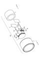
- FIG. 2 is an exploded perspective view of FIG.
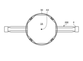
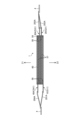
- FIG. 3 is a schematic diagram of the liquid crystal panel, the flexible printed circuit board, and the relay board as viewed from the front side.
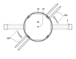
- FIG. 4 is a schematic diagram of the liquid crystal panel, the flexible printed circuit board, and the relay board as viewed from the back side.
- FIG. 5 is a schematic diagram showing a state in which the liquid crystal panel and the flexible printed circuit board are rotated, and corresponds to FIG.
- FIG. 6 is an exploded perspective view of the four liquid crystal panels and the flexible printed circuit board.
- FIG. 7 is a cross-sectional view showing a state in which four liquid crystal panels are stacked.
- FIG. 8 is a cross-sectional view of a liquid crystal panel.
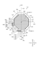
- FIG. 9 is a schematic diagram of a liquid crystal panel viewed from the front side.
- FIG. 10 is a schematic diagram showing the surface of a first substrate included in a liquid crystal panel.
- FIG. 11 is a schematic diagram showing the surface of a second substrate included in a liquid crystal panel.
- FIG. 12 is a cross-sectional view taken along line XII-XII in FIG.
- FIG. 13 is a schematic diagram showing an example in which a light distribution pattern rotates.
- FIG. 14A is a cross-sectional view of a liquid crystal panel, showing the alignment state of liquid crystal molecules when no voltage is applied to the electrodes that drive the liquid crystal.
- FIG. 14A is a cross-sectional view of a liquid crystal panel, showing the alignment state of liquid crystal molecules when no voltage is applied to the electrodes that drive the liquid crystal.
- FIG. 14B is a cross-sectional view of the liquid crystal panel, showing the alignment state of the liquid crystal molecules when a voltage is applied to the electrodes that drive the liquid crystal.
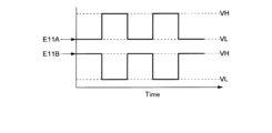
- FIG. 14C is a diagram showing the waveform of a control signal applied to an electrode that drives the liquid crystal.
- FIG. 15A is a schematic perspective view of a liquid crystal panel, showing the arrangement of first and second drive electrodes.
- FIG. 15B is a schematic perspective view of the liquid crystal panel, showing the alignment state of the liquid crystal molecules when a voltage is applied to the second drive electrode.
- FIG. 16 is a diagram showing a schematic diagram of how P waves and S waves are diffused when a second liquid crystal panel is laminated on a first liquid crystal panel.
- FIG. 17 is a diagram for explaining a schematic state in which P waves and S waves are diffused by the four liquid crystal panels according to the first embodiment.
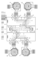
- FIG. 18 is a schematic diagram showing the overall configuration of the liquid crystal panel, relay board, and control board according to the first embodiment.
- FIG. 19A is a schematic diagram showing the arrangement of the first and second substrates in each of the four liquid crystal panels.
- FIG. 19B is a diagram generally explaining the polarized waves acting on each of the four liquid crystal panels, the diffusion direction of the polarized waves, and the potentials of the terminals.
- FIG. 20A is a diagram showing the waveform of a control signal applied to an electrode that drives a liquid crystal in a light distribution pattern with a narrow light distribution.
- FIG. 20B is an image showing a light distribution pattern with a narrow light distribution.
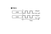
- FIG. 21A is a diagram showing the waveform of a control signal applied to an electrode that drives a liquid crystal in a light distribution pattern of a horizontal line light distribution.
- FIG. 21B is an image showing a light distribution pattern of a horizontal line light distribution.
- FIG. 22 is a diagram for explaining a schematic state in which a light distribution pattern of horizontal line light distribution is formed by four liquid crystal panels.
- FIG. 23A is a diagram showing the waveform of a control signal applied to an electrode that drives a liquid crystal in a light distribution pattern of vertical line light distribution.
- FIG. 23B is an image showing a light distribution pattern of vertical line light distribution.
- FIG. 24 is a diagram for explaining a schematic state in which a light distribution pattern of vertical line light distribution is formed by four liquid crystal panels.
- FIG. 25A is a diagram showing the waveform of a control signal applied to an electrode that drives a liquid crystal in a light distribution pattern of an elliptical light distribution.
- FIG. 25B is an image showing a light distribution pattern of an elliptical light distribution.
- FIG. 26A is a diagram showing waveforms of control signals applied to electrodes that drive liquid crystal in a circular light distribution pattern.
- FIG. 26B is an image showing a light distribution pattern of a circular light distribution.
- FIG. 27 is a schematic diagram showing the overall configuration of a liquid crystal panel, a relay board, and a control board according to the second embodiment.
- FIG. 25A is a diagram showing the waveform of a control signal applied to an electrode that drives a liquid crystal in a light distribution pattern of an elliptical light distribution.
- FIG. 25B is an image showing a light distribution
- FIG. 28 is a cross-sectional view showing a state in which four liquid crystal panels are stacked.
- FIG. 29A is a schematic diagram showing the arrangement of the first and second substrates in each of the four liquid crystal panels.
- FIG. 29B is a diagram generally explaining the polarized waves acting on each of the four liquid crystal panels, the diffusion direction of the polarized waves, and the potentials of the terminals.
- FIG. 30A is a diagram showing waveforms of control signals applied to electrodes that drive liquid crystal in a light distribution pattern of a cross light distribution.
- FIG. 30B is an image showing a light distribution pattern of a cross light distribution.
- FIG. 31 is a diagram for explaining a schematic state in which a light distribution pattern with a cross light distribution is formed by four liquid crystal panels.
- FIG. 1 is a schematic cross-sectional view of a lighting device according to a first embodiment.
- FIG. 2 is an exploded perspective view of FIG. 1.
- FIG. 3 is a schematic view of a liquid crystal panel, a flexible printed circuit board, and a relay board viewed from the front side.
- FIG. 4 is a schematic view of a liquid crystal panel, a flexible printed circuit board, and a relay board viewed from the back side.
- FIG. 5 is a schematic view showing a state in which the liquid crystal panel and the flexible printed circuit board are rotated, and corresponds to FIG. 4.
- FIG. 6 is an exploded perspective view of four liquid crystal panels and a flexible printed circuit board.
- FIG. 7 is a cross-sectional view showing a state in which four liquid crystal panels are stacked.
- the lighting device 100 includes an optical element 1, a holding member 2, a held member 3, a relay board 4, a control board 5, a flexible printed circuit board 200, a wire harness 210, and an LED (light source) 110.
- the holding member 2 is a cylindrical member having a central axis AX.
- the holding member 2 rotates relative to the held member 3 in a direction around the central axis AX.
- the four liquid crystal panels 1A rotate in a direction around the central axis AX.
- the central axis AX extends in the Z direction (axial direction, first direction).
- the axial direction of the central axis AX is the same as the Z direction and the first direction.
- a protrusion 53 protrudes radially inward.
- the protrusion 53 is connected in a ring shape around the entire inner circumference of the holding member 2.
- the held member 3 is a cylindrical member having a central axis AX.
- the tip of the held member 3 fits into the inner circumference of the holding member 2.
- the outer circumference of the held member 3 is provided with a groove 54 that is recessed radially inward.
- the protrusion 53 of the holding member 2 fits into the groove 54. This allows the holding member 2 to rotate in a direction around the central axis AX relative to the held member 3.
- the optical element 1 is, for example, a plurality of liquid crystal panels 1A. As shown in FIG. 6 and FIG. 7, the optical element 1 includes, for example, a first liquid crystal panel 10, a second liquid crystal panel 20, a third liquid crystal panel 30, and a fourth liquid crystal panel 40. Specifically, the first liquid crystal panel 10, the second liquid crystal panel 20, the third liquid crystal panel 30, and the fourth liquid crystal panel 40 are stacked in the axial direction in order from the LED 110. In other words, the first liquid crystal panel 10, the second liquid crystal panel 20, the third liquid crystal panel 30, and the fourth liquid crystal panel 40 are stacked in the order from the Z2 side to the Z1 side, as shown in FIG. 3 and FIG.
- one liquid crystal panel is attached to the back side of a ring-shaped (annular) frame 50, and four of these frames 50 and one liquid crystal panel are stacked in the Z direction (axial direction) in a set state.
- the liquid crystal panels adjacent in the axial direction are bonded to each other via an adhesive layer 57.
- the adhesive layer 57 is a light-transmitting functional film having double-sided adhesiveness, such as OCA (Optical Clear Adhesive).
- the frame 50 is fixed to the inner circumference of the holding member 2. That is, the liquid crystal panel 1A is fixed to the holding member 2 via the frame 50.
- the frame 50 is attached with a cylindrical member 52.
- the flexible printed circuit board 200 includes four flexible printed circuit boards 201A, 202A, 203A, and 204A. As shown in FIG. 6 and FIG. 7, the flexible printed circuit board 201A is bonded to the first liquid crystal panel 10, the flexible printed circuit board 202A is bonded to the second liquid crystal panel 20, the flexible printed circuit board 203A is bonded to the third liquid crystal panel 30, and the flexible printed circuit board 204A is bonded to the fourth liquid crystal panel 40.
- the flexible printed circuit boards 201A and 203A extend in the same direction, and the flexible printed circuit boards 202A and 204A extend in the same direction. Flexible printed circuit boards 201A and 203A and flexible printed circuit boards 202A and 204A extend in opposite directions.
- the relay board 4 is attached to the outer periphery of the cylindrical member 52. That is, the relay board 4 is fixed to the holding member 2 via the cylindrical member 52 and the frame 50. As shown in FIG. 2, the relay board 4 has two relay boards 4A and 4B.
- the relay board 4B includes a board body 44 and connectors 634, 635, and 636 (see FIG. 18).
- the connectors 634, 635, and 636 are provided on the board body 44.
- the connector 636 is disposed closer to the held member 3 in the board body 44, and the connectors 634 and 635 are disposed closer to the holding member 2 in the board body 44.
- the connector 636 is disposed on the Z2 side of the board body 44, and the connectors 634 and 635 are disposed on the Z1 side of the board body 44.
- the wire harness 210 is connected to the connector 636.
- the flexible printed circuit board 200 is connected to the connectors 634 and 635.
- relay board 4A has the same configuration as relay board 4B, and the specific connections are as shown in Figure 18, which will be described later.
- the heat sink 55 is attached to the inner circumference of the held member 3 via the mounting member 56.
- the LED 110 is fixed to the surface on the Z1 side of the heat sink 55. That is, the LED 110 is fixed to the held member 3 via the heat sink 55 and the mounting member 56.
- control board 5 is attached to the inner circumference of the held member 3.
- the control board 5 controls the liquid crystal panel 1A.
- the flexible printed circuit board 200 electrically connects the liquid crystal panel 1A and the relay board 4.
- the wire harness 210 electrically connects the relay board 4 and the control board 5.
- the flexible printed circuit board 200 and the wire harness 210 extend along the axial direction (Z direction). The length of the flexible printed circuit board 200 is shorter than the length of the wire harness 210.
- the holding member 2 rotates relative to the held member 3.
- the wire harness 210 is in a slack state when the rotation angle of the holding member 2 relative to the held member 3 is 0 degrees. And, even when the rotation angle of the holding member 2 relative to the held member 3 is 360 degrees (the holding member 2 has rotated one revolution relative to the held member 3), the wire harness 210 is still in a slack state and has excess length.
- Fig. 8 is a cross-sectional view of a liquid crystal panel.
- Fig. 9 is a schematic diagram of a liquid crystal panel viewed from the front side.
- Fig. 10 is a schematic diagram showing a surface of a first substrate included in the liquid crystal panel.
- Fig. 11 is a schematic diagram showing a surface of a second substrate included in the liquid crystal panel.
- Fig. 12 is a cross-sectional view taken along line XII-XII in Fig. 10.
- the liquid crystal panel 1A includes a first substrate S11 and a second substrate S12 disposed on the Z1 side of the first substrate S11.
- the liquid crystal panel 1A is a regular octagon in plan view, and has a first side 11, a second side 12, a third side 13, a fourth side 14, a fifth side 15, a sixth side 16, a seventh side 17, and an eighth side 18.
- the outer shape of the liquid crystal panel 1A is not particularly limited, and polygons other than an octagon, as well as circles and ellipses, are also included in the present invention.
- the liquid crystal panels 1A stacked in the Z direction (axial direction) are four liquid crystal panels 1A each having the same configuration.
- the first side 11 is located on the Y1 side of the liquid crystal panel 1A.
- the first side 11 is parallel to the X direction in the figure.
- the first side 11 of the liquid crystal panel 1A coincides with the first side 211 of the first substrate S11 shown in FIG. 10.
- the first side 311 of the second substrate S12 shown in FIG. 11 is located on the Y2 side of the first side 211 of the first substrate S11. Therefore, as shown in FIG. 10, when the second substrate S12 is stacked on the front side of the first substrate S11, the end 2Ac of the first substrate S11 on the Y1 side is exposed.
- a first terminal group 10A is provided on the end 2Ac.
- the second side 12 is located on the X1 side of the liquid crystal panel 1A.
- the second side 12 is parallel to the Y direction in the figure.
- the second side 12 of the liquid crystal panel 1A coincides with the second side 212 of the first substrate S11 shown in FIG. 10.
- the second side 312 of the second substrate S12 shown in FIG. 11 is located on the X2 side of the second side 212 of the first substrate S11. Therefore, as shown in FIG. 9, when the second substrate S12 is stacked on the front side of the first substrate S11, the end 2Ad on the X1 side of the first substrate S11 is exposed.
- a second terminal group 20A is provided on the end 2Ad.
- the third side 13 intersects in both the X1 and Y1 directions.
- the intersection angle is 45 degrees.
- the third side 13 coincides with the third side 213 of the first substrate S11 shown in FIG. 10.
- the third side 313 of the second substrate S12 shown in FIG. 11 is located on the X2 and Y2 sides of the third side 213 of the first substrate S11.
- the third side 313 of the second substrate S12 is located closer to the center than the third side 213 of the first substrate S11. Therefore, as shown in FIG. 9, when the second substrate S12 is stacked on the front side of the first substrate S11, the end 2Ae of the first substrate S11 is exposed.
- the fourth side 14 intersects with both the X1 direction and the Y2 direction.
- the intersection angle is 45 degrees.
- the fourth side 14 overlaps with the fourth side 214 of the first substrate S11 shown in FIG. 10 and the fourth side 314 of the second substrate S12 shown in FIG. 11.
- the fifth side 15 is located on the Y2 side of the liquid crystal panel 1A.
- the fifth side 15 overlaps with the fifth side 215 of the first substrate S11 shown in FIG. 10 and the fifth side 315 of the second substrate S12 shown in FIG. 12.
- the sixth side 16 intersects with both the X2 direction and the Y2 direction.
- the intersection angle is 45 degrees.
- the sixth side 164 overlaps with the sixth side 216 of the first substrate S11 shown in FIG. 10 and the sixth side 316 of the second substrate S12 shown in FIG. 11.
- the seventh side 17 is located on the X2 side of the liquid crystal panel 1A.
- the seventh side 17 overlaps with the seventh side 217 of the first substrate S11 shown in FIG. 10 and the seventh side 317 of the second substrate S12 shown in FIG. 11.
- the eighth side 18 intersects with both the X2 direction and the Y1 direction.
- the intersecting angle is 45 degrees.
- the eighth side 18 overlaps with the eighth side 218 of the first substrate S11 shown in FIG. 10 and the eighth side 318 of the second substrate S12 shown in FIG. 11.
- the first terminal group 10A provided at the end 2Ac of the first substrate S11 and the second terminal group 20A provided at the end 2Ad are exposed.
- the first terminal group 10A or the second terminal group 20A is electrically connected to the flexible printed circuit board 200.
- Figure 10 shows a center line CL1 that passes through the center of the first substrate S11 in the X direction and extends in the Y direction, and a center line CL2 that passes through the center of the first substrate S11 in the Y direction and extends in the X direction.
- Figure 11 also shows center lines CL1 and CL2.
- the first terminal group 10A is provided at the first end 21A (indicated by a two-dot chain line) that is closer to the second side 212 (or the third side 213) than the center of the first side 211. That is, the end 2Ac is the end on the Y1 side of the first substrate S11, and the first end 21A indicated by the two-dot chain line is disposed on the X1 side of the center line CL1 of the portion of the end 2Ac.
- the first terminal group 10A is provided at the first end 21A. As shown in FIG.
- the first terminal group 10A includes a first terminal 101, a second terminal 102, a third terminal 103, and a fourth terminal 104.
- the first terminal 101, the second terminal 102, the third terminal 103, and the fourth terminal 104 are arranged in sequence in the X direction from the X1 side to the X2 side.
- These terminals 101, 102, 103, and 104 have a pair of short sides 105 parallel to the first side 211 and a pair of long sides 106 parallel to the second side 212.
- the second terminal group 20A is provided at the second end 22A (indicated by a two-dot chain line) on the first side 211 side (or the third side 213 side) of the end 2Ad along the second side 212 of the first substrate S11 from the center of the second side 212. That is, the end 2Ad is the end on the X1 side of the first substrate S11, and the second end 22A shown by the two-dot chain line is arranged on the Y1 side of the center line CL2 of the portion of the end 2Ad.
- the second terminal group 20A is provided at the second end 22A. As shown in FIG.
- the second terminal group 20A includes a fifth terminal 201, a sixth terminal 202, a seventh terminal 203, and an eighth terminal 204.
- the fifth terminal 201, the sixth terminal 202, the seventh terminal 203, and the eighth terminal 204 are arranged in sequence in the X direction from the X1 side to the X2 side.
- These terminals 201, 202, 203, and 204 have a pair of long sides 107 parallel to the first side 211 and a pair of short sides 108 parallel to the second side 212.
- the wiring of the first substrate S11 and the second substrate S12 will be described.
- the wiring is provided on the front surface.
- the surface on which the wiring is provided is referred to as the front surface
- the surface opposite the front surface is referred to as the back surface.
- connection part C1 of the first substrate S11 and connection part C3 of the second substrate S12 are electrically connected via conductive pillar 58 (see FIG. 8).
- connection part C2 of the first substrate S11 and connection part C4 of the second substrate S12 are electrically connected via conductive pillar 58 (see FIG. 8).
- the first terminal 101 and the fifth terminal 201 are electrically connected via a wiring 241.
- a branch point 242 is provided midway along the wiring 241, and the wiring extends from the branch point 242 to the connection point C1.
- the second terminal 102 and the sixth terminal 202 are electrically connected via wiring 243 and 245.
- a branch point 244 is provided in wiring 243, and wiring 246 extends from branch point 244 to end 247.
- the third terminal 103 and the seventh terminal 203 are electrically connected via wiring 248.
- the fourth terminal 104 and the eighth terminal 204 are electrically connected via wiring 249, 251.
- Wiring 249 extends from the fourth terminal 104 towards the X2 side to a branch point 250.
- Wiring 251 extends from the branch point 250 to the eighth terminal 204.
- a wiring extends from the branch point 250 to a connection point C2.
- the drive electrodes in the liquid crystal panel 1A include a drive electrode (first drive electrode) E11 and a drive electrode (second drive electrode) E12.
- the driving electrode E11 includes a driving electrode E11A and a driving electrode E11B.
- the driving electrode E12 includes a driving electrode E12A and a driving electrode E12B.
- the multiple drive electrodes E11A are connected to wiring 243 and 246.
- the drive electrodes E11A extend linearly along the Y direction.
- the drive electrodes E11A are arranged at equal intervals in the X direction.
- the multiple driving electrodes E11B are connected to wiring 248.
- the driving electrodes E11B extend linearly along the Y direction.
- the driving electrodes E11B are arranged at equal intervals in the X direction.
- the driving electrodes E11A and E11B are arranged alternately in the X direction.
- wiring, drive electrodes, and connection parts are provided on the surface 3Aa of the second substrate S12. Note that the center lines CL1 and CL2 shown in FIG. 11 correspond to the center lines CL1 and CL2 shown in FIG. 10.
- Connection C3 is connected to wires 342 and 343 via branch point 341.
- Wire 342 extends to end 348.
- Wire 343 extends to end 349.
- Connection C4 is connected to wires 345 and 346 via branch point 344.
- Wire 346 extends to end 347.
- the multiple drive electrodes E12A are connected to wiring 342 and 343.
- the drive electrodes E12A extend linearly along the Y direction.
- the drive electrodes E12A are arranged at equal intervals in the X direction.
- the multiple driving electrodes E12B are connected to wiring 346.
- the driving electrodes E12B extend linearly along the X direction.
- the driving electrodes E12B are arranged at equal intervals in the Y direction.
- the driving electrodes E12A and E12B are arranged alternately in the Y direction.
- the liquid crystal panel 1A includes a first substrate S11, a second substrate S12, and a liquid crystal layer LC1 (60).
- the second substrate S12 is disposed on the front side (Z1 side) of the first substrate S11.
- a liquid crystal layer LC1 is provided between the second substrate S12 and the first substrate S11. That is, the surface 2Aa of the first substrate S11 and the surface 3Aa of the second substrate S12 are disposed to face each other with the liquid crystal layer LC1 in between.
- the opposite side of the surface 2Aa of the first substrate S11 is the back surface 2Ab
- the opposite side of the surface 3Aa of the second substrate S12 is the back surface 3Ab.
- the third terminal 103 provided on the surface 2Aa of the first substrate S11 is exposed.
- the insulating layer is provided to prevent contact between the two wires, but in the liquid crystal panel 1A according to this embodiment, the first substrate S11 does not have any overlapping wires, so no insulating layer is provided.
- alignment films AL11, AL12 are laminated on both substrates and electrodes. Specifically, alignment film AL11 is laminated on surface 2Aa of first substrate S11, driving electrodes E11A, 262, and part of the upper surface of wiring 248. Furthermore, alignment film AL12 is laminated on surface 3Aa of second substrate S12 and the upper surface of driving electrode E12A. The first substrate S11 and second substrate S12 are then bonded together by a sealing member 59 that surrounds the effective area, and the space formed by the sealing member 59 is filled with liquid crystal layer LC1.
- FIG. 13 is a schematic diagram showing an example of a rotating light distribution pattern.
- Light distribution pattern 600 is an elliptical light distribution pattern with its major axis along the Y axis. This is the light distribution pattern seen from the Z1 side when, for example, in some or all of the four liquid crystal panels 1A, there is no potential difference between adjacent electrodes of multiple electrodes that extend in the Y direction and are aligned in the X direction, but there is a potential difference between adjacent electrodes of multiple electrodes that extend in the X direction and are aligned in the Y direction. Note that the ratio of the Y axis to the X axis of the elliptical shape depends on the potential difference.
- Light distribution pattern 601 is an elliptical light distribution pattern with its major axis aligned along the X-axis. This is the light distribution pattern seen from the Z1 side when, for example, in some or all of the four liquid crystal panels 1A, there is no potential difference between adjacent electrodes of multiple electrodes that extend in the Y direction and are aligned in the X direction, but there is a potential difference between adjacent electrodes that extend in the X direction and are aligned in the Y direction. Note that the ratio of the Y axis to the X axis of the elliptical shape depends on the potential difference.
- Light distribution pattern 602 is an elliptical light distribution pattern with its major axis tilted 45 degrees counterclockwise (left-handed) with respect to the X-axis. This can be obtained, for example, by rotating all four liquid crystal panels 1A from the state of light distribution pattern 601 by 45 degrees counterclockwise (left-handed) around the central axis AX.
- Light distribution pattern 603 is an elliptical light distribution pattern with its major axis tilted 45 degrees counterclockwise (left-handed) with respect to the Y axis. This can be obtained, for example, by rotating all four liquid crystal panels 1A from the state of light distribution pattern 600 by 45 degrees counterclockwise (left-handed) around the central axis AX.
- FIG. 14A is a cross-sectional view of a liquid crystal panel, and is a diagram showing the alignment state of liquid crystal molecules when no voltage is applied to the electrodes that drive the liquid crystal.
- FIG. 14B is a cross-sectional view of a liquid crystal panel, and is a diagram showing the alignment state of liquid crystal molecules when a voltage is applied to the electrodes that drive the liquid crystal.
- FIG. 14C is a diagram showing the waveform of a control signal applied to the electrodes that drive the liquid crystal.
- FIG. 15A is a schematic perspective view of a liquid crystal panel, and is a diagram showing the arrangement of a first drive electrode and a second drive electrode.
- FIG. 15B is a schematic perspective view of a liquid crystal panel, and is a diagram showing the alignment state of liquid crystal molecules when a voltage is applied to the second drive electrode. Note that FIGS. 14A and 14B are views of the liquid crystal panel from the direction of the arrow 610 in FIG. 15A, and FIG. 15B is a view of the liquid crystal panel from the direction of the arrow 620 in FIG. 15A.
- FIG. 14A shows that the orientation direction of the first alignment film AL11 and the orientation direction of the second alignment film AL12 are different in the first liquid crystal panel 10.
- the first alignment film AL11 is aligned in the X direction
- the second alignment film AL12 is aligned in the Y direction.
- the orientation direction of the first alignment film AL11 and the orientation direction of the second alignment film AL12 are approximately orthogonal.
- the initial light distribution direction on the first substrate S11 side of the first liquid crystal panel 10 is orthogonal (intersects) with the initial light distribution direction on the second substrate S12 side when viewed from the Z direction.
- the orientation process may be a rubbing process or a light distribution process.
- the orientation direction of the alignment film can be set within a range of 90 degrees ⁇ 10 degrees with respect to the extension direction of the drive electrode E11.
- the liquid crystal molecules 60A in the first liquid crystal layer LC1 are aligned such that the long axis direction of the liquid crystal molecules 60A is twisted 90 degrees from the first alignment film AL11 to the second alignment film AL12 when not subjected to the action of an external electric field.
- Figure 14A shows a state in which no voltage is applied to the drive electrodes E11A and E11B. Therefore, as shown in Figure 14A, the long axis direction of the liquid crystal molecules 60A is twisted 90 degrees from the first alignment film AL11 to the second alignment film AL12.
- FIG. 14A shows an example in which a positive type twisted nematic liquid crystal (TN liquid crystal) is used as the first liquid crystal layer LC1, and the long axes of the liquid crystal molecules 60A are aligned in the same direction as the alignment direction of the alignment film.
- the liquid crystal layer 60 preferably contains a chiral agent that imparts a twist to the liquid crystal molecules 60A.
- a low-level voltage VL is applied to the driving electrode E11A
- a high-level voltage VH is applied to the driving electrode E11B.
- pulse voltages of the same amplitude and opposite polarity during the same period are applied to each of the two driving electrodes E11A, E11B.
- a transverse electric field is generated between the driving electrodes E11A and E11B.
- the alignment direction of the liquid crystal molecules 60A on the first substrate S11 side is changed by the influence of the transverse electric field. For example, the alignment of the liquid crystal molecules 60A on the first substrate S11 side is changed so that the long axis direction is parallel to the direction of the electric field.
- the values of the low-level voltage VL and high-level voltage VH applied to the driving electrodes E11A and E11B are set appropriately. For example, 0V is applied as the low-level voltage VL1, and a voltage between 5V and 30V is applied as the high-level voltage VH1. A voltage in which the low-level voltage VL and the high-level voltage VH alternate periodically is applied to the driving electrodes E11A and E11B (see FIG. 14C).
- the frequency of the voltage applied to the drive electrode E11A and the drive electrode E11B can be any frequency that allows the liquid crystal molecules to follow changes in the electric field, for example, 15 Hz or more and 100 Hz or less.
- the refractive index of liquid crystal changes depending on the orientation state.
- the long axis direction of the liquid crystal molecules 60A is aligned horizontally to the surface of the substrate, and is aligned in a state twisted by 90 degrees from the first substrate S11 side to the second substrate S12 side.
- the first liquid crystal layer LC1 has a nearly uniform refractive index distribution in this orientation state.
- the S wave of the light incident on the first liquid crystal panel 10 and the P wave perpendicular to the S wave are rotated due to the influence of the initial orientation of the liquid crystal molecules 60A, but are transmitted through the first liquid crystal layer LC1 in the Z direction with almost no refraction (or scattering).
- the optical rotation refers to the change in the direction of polarization of the polarized component as it passes through the liquid crystal layer 60, and hereinafter refers to the change of the P polarized component (P wave) to the S polarized component (S wave) and the S polarized component (S wave) to the P polarized component (P wave) as it passes through the liquid crystal layer 60 of each liquid crystal panel 1A.
- the first liquid crystal layer LC1 in the ON state where a voltage is applied to the driving electrodes E11A and E11B to form an electric field, if the first liquid crystal layer LC1 has positive dielectric anisotropy, the liquid crystal molecules are oriented with their major axes aligned along the electric field. As a result, as shown in Figure 14B, the first liquid crystal layer LC1 is formed with regions where the liquid crystal molecules 60A stand almost vertically above the driving electrodes E11A and E11B, regions where they are oriented obliquely in line with the distribution of the electric field between the driving electrodes E11A and E11B, and regions away from the driving electrodes E11A and E11B where the initial alignment state is maintained.
- the long axis of the liquid crystal molecules 60A is aligned in a convex arc shape along the direction of the electric field. That is, as shown in FIG. 14A and FIG. 14B, the direction of the initial alignment of the liquid crystal molecules 60A is the same as the direction of the horizontal electric field generated between the driving electrodes E11A and E11B, and as shown in FIG. 14B, the alignment direction of the liquid crystal molecules 60A located approximately in the center between the two electrodes hardly changes, but the liquid crystal molecules located from the center to each electrode side are aligned inclined (tilted) in the normal direction to the surface of the first substrate S11 according to the electric field intensity distribution. Therefore, when the liquid crystal on the first substrate S11 side is viewed as a whole, the liquid crystal molecules 60A are aligned in an arc shape between the driving electrodes E11A and E11B.
- the liquid crystal layer 60 is sufficiently thick, with the cell gap G between the substrates being approximately 15 ⁇ m to 50 ⁇ m, so that the diffusion of different polarized components can be controlled independently on the first substrate S11 side and the second substrate S12 side.
- the liquid crystal molecules 60A have a refractive index anisotropy ⁇ n
- the liquid crystal layer 60 in the on state has a refractive index distribution or retardation distribution according to the orientation state of the liquid crystal molecules 60A.
- retardation is expressed as ⁇ n ⁇ d, where d is the thickness of the liquid crystal layer 60.
- the S wave or P wave is affected by the refractive index distribution of the liquid crystal layer 60 and is scattered when passing through the liquid crystal layer 60.
- the driving electrodes in the second liquid crystal panel 20 include a driving electrode (first driving electrode) E21 and a driving electrode (second driving electrode) E22.
- the driving electrode E21 includes a driving electrode E21A and a driving electrode E21B
- the driving electrode E22 includes a driving electrode E22A and a driving electrode E22B.
- the configuration of the second liquid crystal panel 20 is the same as that of the first liquid crystal panel 10, and the second liquid crystal panel 20 is laminated on the first liquid crystal panel 10 as it is (at a rotation angle of 0° with respect to the Z-axis direction). It is also possible to adopt a configuration in which the second liquid crystal panel 20 is laminated on the first liquid crystal panel 10 in a state rotated 180 degrees in the Z-axis direction.
- the S wave parallel to the X-axis that is incident on the first liquid crystal panel 10 is rotated as it passes through the first liquid crystal layer LC1, and becomes a polarized component parallel to the Y-axis on the second substrate S12 side. That is, the S wave has a polarization axis in the X-axis direction on the first substrate S11 side, but the polarization axis gradually changes as it passes through the first liquid crystal layer LC1 in the Z direction, and becomes a P wave with a polarization axis in the Y-axis direction on the second substrate S12 side, and is emitted from the second substrate S12 side. In this way, the S wave on the first substrate S11 side is rotated as it passes through the liquid crystal layer 60, and becomes a P wave on the second substrate S12 side.
- the S-waves on the first substrate S11 side have a polarization axis parallel to the alignment direction of the liquid crystal molecules 60A of the first liquid crystal layer LC1 on the first substrate S11 side, so they diffuse in the X-axis direction in response to changes in the refractive index distribution of the liquid crystal molecules 60A.
- the P-waves on the second substrate S12 side diffuse in the Y-axis direction in response to changes in the refractive index distribution of the liquid crystal molecules 60A.
- the polarization axis of the P waves is perpendicular to the alignment direction of the liquid crystal molecules 60A on the first substrate S11 side of the first liquid crystal layer LC1, so they are not affected by the refractive index distribution of the liquid crystal molecules 60A and pass through without diffusing.
- the polarization axis of the P waves is also perpendicular to the alignment direction of the liquid crystal molecules 60A, so they are not affected by the refractive index distribution of the liquid crystal molecules 60A and pass through without diffusing.
- the P waves incident on the first liquid crystal panel 10 are rotated in the process of passing through the first liquid crystal panel 10, becoming S waves, and are emitted from the second substrate S12 without being diffused by the first liquid crystal layer LC1.
- the direction of the initial light distribution on the first substrate S21 side of the second liquid crystal panel 20 is perpendicular (intersecting) to the direction of the initial light distribution on the second substrate S22 side when viewed from the Z direction.
- the direction of the initial light distribution on the first substrate S21 side of the second liquid crystal panel 20 is the same as the direction of the initial light distribution on the first substrate S11 side of the first liquid crystal panel 10 when viewed from the Z direction.
- the second liquid crystal layer LC2 of the second liquid crystal panel 20 has a refractive index distribution similar to that of the first liquid crystal layer LC1 of the first liquid crystal panel 10. Therefore, the second liquid crystal panel 20 also experiences the same phenomenon as the first liquid crystal panel 10.
- the polarization axes of the initial S wave and P wave are switched by passing through the first liquid crystal panel 10
- the polarization components affected by the refractive index distribution in the second liquid crystal layer LC2 are also switched. That is, in the process of passing through the second liquid crystal panel 20, the initial S wave changes its polarization axis from the Y axis to the X axis direction again, but does not diffuse.
- the initial P wave changes its polarization axis from the X axis to the Y axis direction again, and is diffused by the influence of the refractive index distribution of the second liquid crystal layer LC2. That is, the initial S wave diffuses in the first liquid crystal panel 10 but not in the second liquid crystal panel 20. The initial P wave does not diffuse in the first liquid crystal panel 10 but diffuses in the second liquid crystal panel 20.
- FIG. 17 is a diagram for explaining a schematic state in which P waves and S waves are diffused by the four liquid crystal panels according to the first embodiment.
- the 17 further adds a third liquid crystal panel 30 and a fourth liquid crystal panel 40 to the two first and second liquid crystal panels 10 and 20 shown in FIG. 16. That is, in each of the first liquid crystal panel 10, the second liquid crystal panel 20, the third liquid crystal panel 30, and the fourth liquid crystal panel 40, a transverse electric field is formed on both sides of the two driving electrodes.
- the driving electrodes in the third liquid crystal panel 30 include a driving electrode (first driving electrode) E31 and a driving electrode (second driving electrode) E32. Furthermore, the driving electrode E31 includes a driving electrode E31A and a driving electrode E31B, and the driving electrode E32 includes a driving electrode E32A and a driving electrode E32B.
- the driving electrodes in the fourth liquid crystal panel 40 include a driving electrode (first driving electrode) E41 and a driving electrode (second driving electrode) E42. Furthermore, the driving electrode E41 includes a driving electrode E41A and a driving electrode E41B, and the driving electrode E42 includes a driving electrode E42A and a driving electrode E42B.
- the third liquid crystal panel 30 and the fourth liquid crystal panel 40 have the same configuration as the first liquid crystal panel 10, and the third liquid crystal panel 30 and the fourth liquid crystal panel 40 are stacked in a state rotated by an angle of 90° in the Z-axis direction relative to the second liquid crystal panel 20. Note that it is also possible to adopt a configuration in which either or both of the third liquid crystal panel 30 and the fourth liquid crystal panel 40 are stacked in a state rotated by 270° in the Z-axis direction relative to the first liquid crystal panel 10.
- (diffused light 1X) shown in the table of FIG. 17 indicates that the polarized light component has diffused once in the X-axis direction before reaching the position
- (diffused light 1X1Y) indicates that the polarized light component has diffused once in the X-axis direction and once in the Y-axis direction before reaching the position. The same applies to the others.
- the initial light distribution direction on the first substrate S31 side of the third liquid crystal panel 30 is perpendicular (intersects) to the initial light distribution direction on the second substrate S32 side when viewed from the Z direction.
- the initial light distribution direction on the first substrate S41 side of the fourth liquid crystal panel 40 is perpendicular (intersects) to the initial light distribution direction on the second substrate S42 side when viewed from the Z direction.
- the initial light distribution direction on the first substrate S31 side of the third liquid crystal panel 30 is the same as the initial light distribution direction on the first substrate S41 side of the fourth liquid crystal panel 40.
- the initial light distribution direction on the first substrate S31 side of the third liquid crystal panel 30 and the initial light distribution direction on the first substrate S41 side of the fourth liquid crystal panel 40 are perpendicular (intersect) to the initial light distribution direction on the first substrate S11 side of the first liquid crystal panel 10 and the initial light distribution direction on the first substrate S21 side of the second liquid crystal panel 20.
- the S waves are rotated once to P waves and then rotated again to S waves before being emitted from the second liquid crystal panel 20, and are diffused once each in the X-axis direction and the Y-axis direction in the second liquid crystal panel 20.
- the P waves are rotated once to S waves and then rotated again to P waves before entering the first liquid crystal panel 10 and exiting the second liquid crystal panel 20, and are diffused once each in the X-axis direction and the Y-axis direction in the first liquid crystal panel 10.
- the longitudinal direction of the driving electrode E31 intersects with the driving electrode E11 of the first liquid crystal panel 10 and the driving electrode E21 of the second liquid crystal panel 20 at an angle of 90 degrees ⁇ 10 degrees
- the longitudinal direction of the driving electrode E32 intersects with the driving electrode E12 of the first liquid crystal panel 10 and the driving electrode E22 of the second liquid crystal panel 20 at an angle of 90 degrees ⁇ 10 degrees.
- the longitudinal direction of the driving electrode E41 intersects with the driving electrode E11 of the first liquid crystal panel 10 and the driving electrode E21 of the second liquid crystal panel 20 at an angle of 90 degrees ⁇ 10 degrees
- the longitudinal direction of the driving electrode E42 intersects with the driving electrode E12 and the driving electrode E22 at an angle of 90 degrees ⁇ 10 degrees. Therefore, in the third liquid crystal panel 30 and the fourth liquid crystal panel 40, the phenomenon that occurred in the first liquid crystal panel 10 and the second liquid crystal panel 20 for S waves and P waves is reversed.
- the diffused S wave is rotated 90 degrees in accordance with the twisted alignment of the liquid crystal molecules in the process of traveling from the first substrate S31 side to the second substrate S32 side in the third liquid crystal layer LC3.
- the S wave transitions to a P wave again.
- the polarization direction of the P wave is parallel to the long axis direction of the liquid crystal molecules on the second substrate S32 side.
- the P wave is further diffused in the Y axis direction under the influence of the refractive index distribution of the liquid crystal molecules, and is then emitted. That is, the S waves incident on the third liquid crystal panel 30 transition to P waves while passing through the third liquid crystal panel 30, and are diffused again once in each of the X-axis direction and the Y-axis direction.
- This P wave is emitted from the third liquid crystal panel 30 and enters the fourth liquid crystal panel 40.
- the polarization direction of the P wave is in a direction intersecting with the long axis direction of the liquid crystal molecules 60A on the first substrate S41 side of the fourth liquid crystal layer LC4. Therefore, although the liquid crystal molecules 60A on the first substrate S41 side change their refractive index distribution due to the electric field generated by the driving electrode E41, the P wave is not diffused and continues to the second substrate S42 side.
- the P wave is rotated 90 degrees in accordance with the twisted orientation of the liquid crystal molecules 60A as it travels through the fourth liquid crystal layer LC4 from the first substrate S41 side to the second substrate S42 side. As a result, the P wave transitions to an S wave.
- the polarization direction of the S wave is in a direction intersecting with the long axis direction of the liquid crystal molecules on the second substrate S42 side. Therefore, although the liquid crystal molecules 60A on the second substrate S42 side change their refractive index distribution due to the electric field generated by the driving electrode E12, the S wave is not affected and passes through as it is. That is, the P waves transition to S waves as they pass through the fourth liquid crystal panel 40, but are transmitted through the fourth liquid crystal panel 40 without being diffused or otherwise dispersed.
- the S waves incident on the third liquid crystal panel 30 transition once to P waves and then transition again to S waves before being emitted from the fourth liquid crystal panel 40, and are diffused once each in the X-axis direction and the Y-axis direction by the third liquid crystal panel 30.
- the polarization direction of the P wave incident on the third liquid crystal panel 30 is in a direction intersecting (orthogonal to) the long axis direction of the liquid crystal molecules 60A on the first substrate S31 side of the third liquid crystal layer LC3. Therefore, although the liquid crystal molecules 60A on the first substrate S31 side change their refractive index distribution due to the electric field generated by the driving electrode E31, the P wave is not diffused and goes directly to the second substrate S32 side. In addition, the P wave is rotated 90 degrees in accordance with the twisted orientation of the liquid crystal molecules 60A in the process of traveling from the first substrate S31 side to the second substrate S32 side in the third liquid crystal layer LC3.
- the P wave transitions to an S wave.
- the polarization direction of the S wave is in a direction intersecting with the long axis direction of the liquid crystal molecules 60A on the second substrate S32 side. Therefore, although the liquid crystal molecules 60A on the second substrate S32 side change their refractive index distribution due to the electric field generated by the driving electrode E32, the S wave is not affected and passes directly through. That is, the P waves incident on the third liquid crystal panel 30 are converted to S waves in the process of passing through the third liquid crystal panel 30, but are transmitted through the third liquid crystal panel 30 without being diffused.
- the polarization direction of the S wave is parallel to the long axis direction of the liquid crystal molecules 60A on the first substrate S41 side of the fourth liquid crystal layer LC4.
- the liquid crystal molecules 60A on the first substrate S41 side of the fourth liquid crystal panel 40 have a refractive index distribution that is changed by the electric field generated by the drive electrode E41, so the S wave is diffused in the X-axis direction.
- this diffused S wave is rotated 90 degrees in accordance with the twisted orientation of the liquid crystal molecules 60A as it travels through the fourth liquid crystal layer LC4 from the first substrate S41 side to the second substrate S42 side.
- the polarization direction of this P wave is parallel to the long axis direction of the liquid crystal molecules 60A on the second substrate S42 side.
- the refractive index distribution of the liquid crystal molecules 60A on the second substrate S42 side is changed by the electric field generated by the drive electrode E42, so this P wave is further influenced by the refractive index distribution of the liquid crystal molecules 60A and diffuses in the Y direction before being emitted from the second substrate S42 side.
- the P waves incident on the third liquid crystal panel 30 transition once to S waves and then transition again to P waves before being emitted from the fourth liquid crystal panel 40, and are diffused once each in the X-axis direction and the Y-axis direction by the fourth liquid crystal panel 40.
- the S waves emitted from the LED 110 are diffused twice in the X-axis direction and twice in the Y-axis direction from the time they enter the first liquid crystal panel 10 until they are emitted from the fourth liquid crystal panel 40.
- the P waves emitted from the LED 110 are diffused twice in the X-axis direction and twice in the Y-axis direction from the time they enter the first liquid crystal panel 10 until they are emitted from the fourth liquid crystal panel 40.
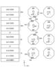
- Fig. 18 is a schematic diagram showing the overall configuration of the liquid crystal panel, relay board, and control board according to the first embodiment.
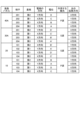
- Fig. 19A is a schematic diagram showing the arrangement of the first board and the second board in each of the four liquid crystal panels.
- Fig. 19B is a diagram generally explaining the polarized waves, the diffusion direction of the polarized waves, and the potentials of the terminals acting on each of the four liquid crystal panels.
- the lighting device 100 includes four liquid crystal panels 1A, two relay boards 4A and 4B, and two control boards 5A and 5B.
- the control board 5A and relay board 4A are electrically connected via a single wire harness 210, which has signal lines 713, 714, 715, and 716.
- the relay board 4A and the first liquid crystal panel 10 are electrically connected via a single flexible printed circuit board 200, which has signal lines 701, 702, 703, and 704.
- the relay board 4A and the third liquid crystal panel 30 are electrically connected via a single flexible printed circuit board 200, which has signal lines 705, 706, 707, and 708.
- the control board 5B and the relay board 4B are electrically connected via a single wire harness 210, and the wire harness 210 has signal lines 733, 734, 735, and 736.
- the relay board 4B and the second liquid crystal panel 20 are electrically connected via a single flexible printed circuit board 200, and the flexible printed circuit board 200 has signal lines 721, 722, 723, and 724.
- the relay board 4B and the fourth liquid crystal panel 40 are electrically connected via a single flexible printed circuit board 200, and the flexible printed circuit board 200 has signal lines 725, 726, 727, and 728.
- the four liquid crystal panels 1A are the first liquid crystal panel 10, the second liquid crystal panel 20, the third liquid crystal panel 30, and the fourth liquid crystal panel 40.
- the first liquid crystal panel 10 and the third liquid crystal panel 30 are electrically connected to the relay substrate 4A via eight signal lines.
- the second liquid crystal panel 20 and the fourth liquid crystal panel 40 are electrically connected to the relay substrate 4B via eight signal lines.
- the relay substrate 4A and the control substrate 5A are electrically connected to each other via four signal lines.
- the relay substrate 4B and the control substrate 5B are electrically connected to each other via four signal lines.
- the relay substrate 4A is provided with connectors 631, 632, and 633.
- the first liquid crystal panel 10 is provided with a first terminal 101 corresponding to the electrode E12A of the second substrate, a second terminal 102 corresponding to the electrode E11A of the first substrate, a third terminal 103 corresponding to the electrode E11B of the first substrate, and a fourth terminal 104 corresponding to the electrode E12B of the second substrate.
- the first terminal 101 and the connector 632 are connected via a signal line 701.
- the second terminal 102 and the connector 632 are connected via a signal line 702.
- the third terminal 103 and the connector 632 are connected via a signal line 703.
- the fourth terminal 104 and the connector 632 are connected via a signal line 704.
- the third liquid crystal panel 30 is also provided with a fifth terminal 201, a sixth terminal 202, a seventh terminal 203, and an eighth terminal 204.
- the fifth terminal 201 and the connector 631 are connected via a signal line 705.
- the sixth terminal 202 and the connector 631 are connected via a signal line 706.
- the seventh terminal 203 and the connector 631 are connected via a signal line 707.
- the eighth terminal 204 and the connector 631 are connected via a signal line 708.
- Signal lines 701 and 707 are electrically connected to signal line 709 via connectors 631 and 632. That is, two signal lines are connected to one signal line on relay board 4A via connectors 631 and 632. Similarly, the other signal lines are connected two by two on relay boards 4A and 5B. Specifically, signal lines 702 and 708 are electrically connected to signal line 710 via connectors 631 and 632. Signal lines 703 and 705 are electrically connected to signal line 711 via connectors 631 and 632. Signal lines 704 and 706 are electrically connected to signal line 712 via connectors 631 and 632.
- one signal line in the relay board 4A is electrically connected to one signal line in the control board 5A via connector 633.
- signal line 709 in the relay board 4A is electrically connected to connector 637 of the control board 5A via signal line 713 of the wire harness 210.
- Signal line 710 in the relay board 4A is electrically connected to connector 637 of the control board 5A via signal line 714 of the wire harness 210.
- Signal line 711 in the relay board 4A is electrically connected to connector 637 of the control board 5A via signal line 715 of the wire harness 210.
- Signal line 712 in the relay board 4A is electrically connected to connector 637 of the control board 5A via signal line 716 of the wire harness 210.
- Signal lines 702, 708, 710, and 714 are at potential A.
- Signal lines 701, 707, 709, and 713 are at potential B.
- Signal lines 704, 706, 712, and 716 are at potential C.
- Signal lines 703, 705, 711, and 715 are at potential D.
- connectors 634, 635, and 636 are provided on relay board 4B.
- first terminal 101, second terminal 102, third terminal 103, and fourth terminal 104 are provided on second liquid crystal panel 20.
- First terminal 101 and connector 634 are connected via signal line 721.
- Second terminal 102 and connector 634 are connected via signal line 722.
- Third terminal 103 and connector 634 are connected via signal line 723.
- Fourth terminal 104 and connector 634 are connected via signal line 724.
- the fourth liquid crystal panel 40 is provided with a fifth terminal 201, a sixth terminal 202, a seventh terminal 203, and an eighth terminal 204.
- the fifth terminal 201 and the connector 635 are connected via a signal line 725.
- the sixth terminal 202 and the connector 635 are connected via a signal line 726.
- the seventh terminal 203 and the connector 635 are connected via a signal line 727.
- the eighth terminal 204 and the connector 635 are connected via a signal line 728.
- Signal lines 721 and 727 are electrically connected to signal line 729 via connectors 634 and 635. That is, two signal lines are connected to one signal line via connectors 634 and 635. Similarly, the other signal lines are connected in pairs. Specifically, signal lines 722 and 728 are electrically connected to signal line 730 via connectors 634 and 635. Signal lines 723 and 725 are electrically connected to signal line 731 via connectors 634 and 635. Signal lines 724 and 726 are electrically connected to signal line 732 via connectors 634 and 635.
- one signal line in relay board 4B is electrically connected to one signal line in control board 5B via connector 636.
- signal line 729 in relay board 4B is electrically connected to signal line 733 in control board 5B.
- Signal line 730 in relay board 4B is electrically connected to signal line 734 in control board 5B.
- Signal line 731 in relay board 4B is electrically connected to signal line 735 in control board 5B.
- Signal line 732 in relay board 4B is electrically connected to signal line 736 in control board 5B.
- Signal lines 722, 728, 730, and 734 are at potential A.
- Signal lines 721, 727, 729, and 733 are at potential B.
- Signal lines 724, 726, 732, and 736 are at potential C.
- Signal lines 723, 725, 731, and 735 are at potential D.
- a first liquid crystal panel 10 As shown in FIG. 19A, in the lighting device 100, a first liquid crystal panel 10, a second liquid crystal panel 20, a third liquid crystal panel 30, and a fourth liquid crystal panel 40 are stacked in order from the side closest to the LED 110.
- the drive electrodes E11 extend in the Y direction as indicated by the hollow arrow, and on the second substrate S12, the drive electrodes E12 extend in the X direction as indicated by the hollow arrow.
- the second liquid crystal panel 20 is rotated 180 degrees clockwise (right-handed) around the central axis AX (see FIG. 4) relative to the first liquid crystal panel 10.
- the drive electrodes E21 extend in the Y direction as indicated by the hollow arrow
- the drive electrodes E22 extend in the X direction as indicated by the hollow arrow.
- the third liquid crystal panel 30 is rotated 270 degrees clockwise (right-handed) around the central axis AX (see FIG. 4) relative to the first liquid crystal panel 10.
- the drive electrode E31 extends in the X direction as indicated by the hollow arrow, and on the second substrate S32, the drive electrode E32 extends in the Y direction as indicated by the hollow arrow.
- the fourth liquid crystal panel 40 is rotated 90 degrees clockwise (right-handed) around the central axis AX (see FIG. 4) relative to the first liquid crystal panel 10.
- the drive electrode E41 On the first substrate S41 of the fourth liquid crystal panel 40, the drive electrode E41 extends in the X direction as indicated by the hollow arrow, and on the second substrate S42, the drive electrode E42 extends in the Y direction as indicated by the hollow arrow.
- the substrate is the second substrate.
- the terminal 101 is electrically connected from the connection C1 of the first substrate S11 to the connection C3 (see FIG. 11) of the second substrate S12 via the conductive pillar 58 (see FIG. 8), and is finally electrically connected to the driving electrode E12A of the second substrate S12.
- the term "direction of the electrode” as the X direction means that the direction in which the driving electrode E12A extends is the X direction.
- potential as the B potential means that the potential of the terminal 101 of the first liquid crystal panel 10 is the B potential, as shown in FIG. 18.
- direction of diffusion of light as the Y direction means that, as described with reference to FIG. 17, on the second substrate S12 side of the first liquid crystal panel 10, the S wave (more specifically, the S wave optically rotated from the incident P wave) diffuses in the Y direction.
- the polarized light that acts refers to the polarized light that diffuses, either P waves or S waves.
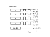
- FIG. 20A is a diagram showing the waveform of a control signal applied to an electrode driving a liquid crystal in a light distribution pattern of narrow light distribution.
- FIG. 20B is an image showing a light distribution pattern of narrow light distribution.
- FIG. 21A is a diagram showing the waveform of a control signal applied to an electrode driving a liquid crystal in a light distribution pattern of horizontal line light distribution.
- FIG. 21B is an image showing a light distribution pattern of horizontal line light distribution.
- FIG. 22 is a diagram showing a state in which a light distribution pattern of horizontal line light distribution is formed by four liquid crystal panels.
- FIG. 23A is a diagram showing the waveform of a control signal applied to an electrode driving a liquid crystal in a light distribution pattern of vertical line light distribution.
- FIG. 23B is an image showing a light distribution pattern of vertical line light distribution.
- FIG. 24 is a diagram showing a state in which a light distribution pattern of vertical line light distribution is formed by four liquid crystal panels.
- FIG. 25A is a diagram showing the waveform of a control signal applied to an electrode driving a liquid crystal in a light distribution pattern of elliptical light distribution.
- FIG. 25B is an image showing a light distribution pattern of elliptical light distribution.
- Fig. 26A is a diagram showing the waveform of a control signal applied to an electrode for driving a liquid crystal in a light distribution pattern of a circular light distribution
- Fig. 26B is an image showing the light distribution pattern of a circular light distribution.
- the light distribution pattern of horizontal line is a line-shaped light distribution pattern that extends long in the horizontal direction (Y direction in this embodiment) (see FIG. 21B).
- the potential B and the potential C have a low level voltage VL of -aV and a high level voltage VH of aV.
- the potential A and the potential D are 0V.
- the potential B and the potential C are pulse voltages that have a first amplitude and are opposite in sign to each other during the same period. Therefore, a pulse voltage is applied to the driving electrode E12 of the first liquid crystal panel 10, the driving electrode E31 of the third liquid crystal panel 30, the driving electrode E22 of the second liquid crystal panel 20, and the driving electrode E41 of the fourth liquid crystal panel 40.
- a pulse voltage having a first amplitude and opposite polarity to each other during the same period is applied to each of the driving electrodes E12A and E12B.
- a pulse voltage having a first amplitude and opposite polarity to each other during the same period is applied to each of the driving electrodes E31A and E31B.
- a pulse voltage having a first amplitude and opposite polarity to each other during the same period is applied to each of the driving electrodes E22A and E22B.
- a pulse voltage having a first amplitude and opposite polarity to each other during the same period is applied to each of the driving electrodes E41A and E41B.
- the operating mode of light diffusion is as shown in FIG. 22. On the left side of FIG. 22, the driving electrodes that form an electric field are hatched.
- the S waves incident on the first liquid crystal panel 10 are not diffused while passing through the first liquid crystal panel 10, but are rotated to P waves while passing through the first liquid crystal panel 10, and are emitted from the first liquid crystal panel 10.
- the P waves incident on the second liquid crystal panel 20 are rotated to S waves while passing through the second liquid crystal panel 20, and are diffused once in the Y direction on the second drive electrode side where a transverse electric field is formed.
- the S waves incident on the third liquid crystal panel 30 are diffused once in the Y direction on the first drive electrode side where a transverse electric field is formed, and are also rotated to P waves while passing through the third liquid crystal panel 30.
- the P waves incident on the fourth liquid crystal panel 40 are not diffused, and are rotated to S waves while passing through the fourth liquid crystal panel 40.
- the P wave incident on the first liquid crystal panel 10 is rotated to an S wave while passing through the first liquid crystal panel 10, diffuses once in the Y direction on the second drive electrode side where a transverse electric field is formed, and is emitted from the first liquid crystal panel 10.
- the S wave incident on the second liquid crystal panel 20 is rotated to a P wave while passing through the second liquid crystal panel 20, and is not diffused while passing through the second liquid crystal panel 20.
- the P wave incident on the third liquid crystal panel 30 is rotated to an S wave while passing through the third liquid crystal panel 30, and is not diffused while passing through the third liquid crystal panel 30.
- the S wave incident on the fourth liquid crystal panel 40 is diffused once in the Y direction on the first drive electrode side where a transverse electric field is formed, and is also rotated to a P wave while passing through the fourth liquid crystal panel 40.
- the S waves are diffused twice in the Y direction, and the P waves are also diffused twice in the Y direction.
- the S waves and P waves are combined and diffused a total of four times in the Y direction. For this reason, as described above, the horizontal line light distribution pattern shown in Figure 21B is formed.
- the vertical line light distribution pattern is a line-shaped light distribution pattern that extends long in the vertical direction (X direction in this embodiment) (see FIG. 23B).
- the potential A and the potential D have a low level voltage VL of -aV and a high level voltage VH of aV.
- the potential B and the potential C are 0V.
- the potential A and the potential D are pulse voltages whose amplitude is the second amplitude and whose positive and negative polarities are opposite to each other during the same period. Therefore, a pulse voltage is applied to the driving electrode E11 of the first liquid crystal panel 10, the driving electrode E32 of the third liquid crystal panel 30, the driving electrode E21 of the second liquid crystal panel 20, and the driving electrode E42 of the fourth liquid crystal panel 40.
- a pulse voltage having a second amplitude and opposite polarity to each other during the same period is applied to each of the driving electrodes E11A and E11B.
- a pulse voltage having a second amplitude and opposite polarity to each other during the same period is applied to each of the driving electrodes E32A and E32B.
- a pulse voltage having a second amplitude and opposite polarity to each other during the same period is applied to each of the driving electrodes E21A and E21B.
- a pulse voltage having a second amplitude and opposite polarity to each other during the same period is applied to each of the driving electrodes E42A and E42B.
- the operating mode of light diffusion is as shown in FIG. 24. On the left side of FIG. 24, the driving electrodes that form an electric field are hatched.
- the S wave incident on the first liquid crystal panel 10 is not diffused while passing through the first liquid crystal panel 10, but is rotated to a P wave while passing through the first liquid crystal panel 10, and is emitted from the first liquid crystal panel 10.
- the P wave incident on the second liquid crystal panel 20 is rotated to an S wave while passing through the second liquid crystal panel 20, and is diffused once in the X direction on the first drive electrode side where a transverse electric field is formed.
- the S wave incident on the third liquid crystal panel 30 is diffused once in the X direction on the second drive electrode side where a transverse electric field is formed, and is also rotated to a P wave while passing through the third liquid crystal panel 30.
- the P wave incident on the fourth liquid crystal panel 40 is not diffused, and is rotated to an S wave while passing through the fourth liquid crystal panel 40.
- the P wave incident on the first liquid crystal panel 10 is rotated to an S wave while passing through the first liquid crystal panel 10, diffuses once in the X direction on the first drive electrode side where a transverse electric field is formed, and is emitted from the first liquid crystal panel 10.
- the S wave incident on the second liquid crystal panel 20 is rotated to a P wave while passing through the second liquid crystal panel 20, and is not diffused while passing through the second liquid crystal panel 20.
- the P wave incident on the third liquid crystal panel 30 is rotated to an S wave while passing through the third liquid crystal panel 30, and is not diffused while passing through the third liquid crystal panel 30.
- the S wave incident on the fourth liquid crystal panel 40 is diffused once in the X direction on the second drive electrode side where a transverse electric field is formed, and is also rotated to a P wave while passing through the fourth liquid crystal panel 40.
- the S waves are diffused twice in the X direction, and the P waves are also diffused twice in the X direction.
- the S waves and P waves are combined and diffused a total of four times in the X direction. For this reason, as described above, the vertical line light distribution pattern shown in FIG. 23B is formed.
- An elliptical light distribution pattern is a vertically elongated elliptical light distribution pattern, for example, as shown in Fig. 25B.
- potential B and potential C have a low level voltage VL of -a'V and a high level voltage VH of a'V.
- potential A and potential D have a low level voltage VL of -b'V and a high level voltage VH of b'V.
- a'V is smaller than b'V.
- -a'V is larger than -b'V.
- potential B and potential C are pulse voltages that have a third amplitude and are opposite in sign to each other during the same period. That is, the second drive electrode E12 in the first liquid crystal panel 10, the first drive electrode E31 in the third liquid crystal panel 30, the drive electrode E22 in the second liquid crystal panel 20, and the drive electrode E41 in the fourth liquid crystal panel 40 each have two drive electrodes that are alternately arranged when viewed from the Z direction, and a pulse voltage that has a third amplitude and is opposite in sign to each other during the same period is applied to each of the two drive electrodes.
- a pulse voltage having a third amplitude and opposite polarity to each other during the same period is applied to each of the driving electrodes E12A and E12B.
- a pulse voltage having a third amplitude and opposite polarity to each other during the same period is applied to each of the driving electrodes E31A and E31B.
- a pulse voltage having a third amplitude and opposite polarity to each other during the same period is applied to each of the driving electrodes E22A and E22B.
- a pulse voltage having a third amplitude and opposite polarity to each other during the same period is applied to each of the driving electrodes E41A and E41B.
- potential A and potential D are pulse voltages whose amplitude is a fourth amplitude different from the third amplitude and whose polarities are opposite to each other during the same period. That is, each of the driving electrode E11 of the first liquid crystal panel 10, the driving electrode E32 of the third liquid crystal panel 30, the driving electrode E21 of the second liquid crystal panel 20, and the driving electrode E42 of the fourth liquid crystal panel 40 has two driving electrodes arranged alternately when viewed from the Z direction, and a pulse voltage whose amplitude is a fourth amplitude and whose polarities are opposite to each other during the same period is applied to each of the two driving electrodes.
- pulse voltages having a fourth amplitude and opposite polarity to each other during the same period are applied to each of the driving electrodes E11A and E11B.
- Pulse voltages having a fourth amplitude and opposite polarity to each other during the same period are applied to each of the driving electrodes E32A and E32B.
- Pulse voltages having a fourth amplitude and opposite polarity to each other during the same period are applied to each of the driving electrodes E21A and E21B.
- Pulse voltages having a fourth amplitude and opposite polarity to each other during the same period are applied to each of the driving electrodes E42A and E42B.
- the S waves incident on the first liquid crystal panel 10 are diffused twice in the X-axis direction and twice in the Y-axis direction before being emitted from the fourth liquid crystal panel 40.
- the P waves incident on the first liquid crystal panel 10 are diffused twice in the X-axis direction and twice in the Y-axis direction before being emitted from the fourth liquid crystal panel 40.
- the P waves are diffused four times in the X-axis direction and four times in the Y-axis direction.
- an elliptical light distribution pattern is formed as shown in FIG. 25B.
- the potential A and the potential B are the same, and the potential C and the potential D are the same.
- the potentials A and B are ⁇ aV of the low level voltage VL and the potentials C and D are aV of the high level voltage VH, and in the next certain period, the potentials A and B are aV of the high level voltage VH and the potentials C and D are ⁇ aV of the low level voltage VL.
- the lighting device 100 includes two control boards 5A, 5B, two relay boards 4A, 4B electrically connected to each of the two control boards 5A, 5B via a wire harness 210, and four liquid crystal panels 1A electrically connected to the two relay boards 4A, 4B via flexible printed circuit boards 200.
- Two of the four liquid crystal panels 1A are electrically connected to the relay board 4A (one of the two relay boards) via a flexible printed circuit board 200.
- the other two of the four liquid crystal panels 1A are electrically connected to the relay board 4B (the other of the two relay boards) via a flexible printed circuit board 200.
- one control board 5 and one relay board 4 are connected via one wire harness 210, and one relay board 4 and two liquid crystal panels 1A are connected via two flexible printed circuit boards 200. That is, the number of wire harnesses 210 connecting the control board 5 and the relay board 4 is half the number of flexible printed circuit boards 200 connecting the liquid crystal panel 1A and the relay board 4.
- the force applied to the connection part between the wire harness 210 and the relay board 4 or the connection part between the wire harness 210 and the control board 5 is smaller than when the number of wire harnesses 210 connecting the control board 5 and the relay board 4 is the same as the number of flexible printed circuit boards 200 connecting the liquid crystal panel 1A and the relay board 4.
- the lighting device 100 that rotates the light distribution pattern around the axis (central axis AX) it is possible to prevent damage to the connection between the wiring (flexible printed circuit board 200) and the liquid crystal panel 1A or the connection between the wiring (wire harness 210) and the control board 5.
- Signal lines are provided on the wire harness 210 and the flexible printed circuit board 200.
- the signal lines of the wire harness 210 are branched at the relay board 4 and connected to the signal lines of the flexible printed circuit board 200.
- the number of control boards 5 can be reduced. Furthermore, by reducing the number of control boards 5, the number of wire harnesses 210 is also reduced, and therefore the number of connection parts between the wire harnesses 210 and the control boards 5 is also reduced. Therefore, the force applied to the connection parts between the wire harnesses 210 and the control boards 5 is reduced, and damage to the connection parts can be suppressed.
- the wire harness 210 is longer than the flexible printed circuit board 200.
- the wire harness 210 When the liquid crystal panel 1A is rotated relative to the control board 5, the wire harness 210 is twisted. However, because the length of the wire harness 210 is longer, the force applied to the connection between the wire harness 210 and the relay board 4 or the connection between the wire harness 210 and the control board 5 is smaller, and damage to the connection can be suppressed. In addition, because the length of the flexible printed circuit board 200 can be set shorter, the axial length of the holding member 2 can be shortened, allowing the lighting device 100 to be made more compact.
- It comprises a holding member 2 that holds four liquid crystal panels 1A and two relay boards 4, and a held member 3 that supports the holding member 2 rotatably around the central axis AX and to which two control boards 5A and 5B are attached.
- the light distribution pattern when the light distribution pattern is elongated in one direction (e.g., vertical or horizontal), the light distribution pattern can be rotated around the central axis AX, making it possible to provide a wide variety of light distribution patterns.
- light distribution pattern 601 which has a long elliptical shape along the Y axis, can be changed to light distribution pattern 602 by rotating it 45 degrees counterclockwise.
- the four liquid crystal panels 1A are stacked in the order of the first liquid crystal panel 10, the second liquid crystal panel 20, the third liquid crystal panel 30, and the fourth liquid crystal panel 40 from the Z2 side (one side in the first direction) to the Z1 side (the other side in the first direction).
- the initial light distribution direction of the first substrate side of the first liquid crystal panel 10 and the second liquid crystal panel 20 is orthogonal (intersects) to the initial light distribution direction of the first substrate side of the third liquid crystal panel 30 and the fourth liquid crystal panel 40 when viewed from the Z direction.
- the relay substrate 4A is electrically connected to the driving electrodes E11, E12, E31, and E32.
- the relay substrate 4B is electrically connected to the driving electrodes E21, E22, E41, and E42.
- the lighting device 100 By configuring the lighting device 100 in this way, it is possible to form a variety of light distribution patterns, including a horizontal line light distribution pattern, a vertical line light distribution pattern, an elliptical light distribution pattern, and a circular light distribution pattern.
- Each of the driving electrode E12 in the first liquid crystal panel 10, the driving electrode E31 in the third liquid crystal panel 30, the driving electrode E22 in the second liquid crystal panel 20, and the driving electrode E41 in the fourth liquid crystal panel 40 has two driving electrodes arranged alternately when viewed from the Z direction, and a pulse voltage having a first amplitude and opposite positive and negative polarities is applied to each of the two driving electrodes during the same period.
- Each of the driving electrode E11 in the first liquid crystal panel 10, the driving electrode E32 in the third liquid crystal panel 30, the driving electrode E21 in the second liquid crystal panel 20, and the driving electrode E42 in the fourth liquid crystal panel 40 has two driving electrodes arranged alternately when viewed from the Z direction, and a pulse voltage having a second amplitude and opposite positive and negative polarities is applied to each of the two driving electrodes during the same period.
- Each of the driving electrode E12 in the first liquid crystal panel 10 and the driving electrode E31 in the third liquid crystal panel 30 has two driving electrodes arranged alternately when viewed from the Z direction, and a pulse voltage having a third amplitude and opposite positive and negative polarities is applied to each of the two driving electrodes during the same period.
- the driving electrode E21 in the second liquid crystal panel 20 and the driving electrode E42 in the fourth liquid crystal panel 40 each have two driving electrodes arranged alternately when viewed from the Z direction, and a pulse voltage having a fourth amplitude different from the third amplitude and opposite positive and negative polarities during the same period is applied to each of the two driving electrodes.
- Each of the drive electrodes E11, E21, E31, E41 and the drive electrodes E12, E22, E32, E42 has two drive electrodes arranged alternately when viewed from the Z direction, and a pulse voltage having a fifth amplitude and opposite positive and negative polarities during the same period is applied to each of the two drive electrodes.
- Fig. 27 is a schematic diagram showing the overall configuration of the liquid crystal panel, relay board, and control board according to the second embodiment.
- Fig. 28 is a cross-sectional view showing a state in which four liquid crystal panels are stacked.
- Fig. 29A is a schematic diagram showing the arrangement of the first and second boards in each of the four liquid crystal panels.
- Fig. 29B is a diagram generally explaining the polarized waves, the diffusion direction of the polarized waves, and the potentials of the terminals acting on each of the four liquid crystal panels.
- the first liquid crystal panel 10, the second liquid crystal panel 20, the third liquid crystal panel 30A and the fourth liquid crystal panel 40A are stacked in order from the side closest to the LED 110 of the light source.
- a flexible printed circuit board 201A is bonded to the first liquid crystal panel 10
- a flexible printed circuit board 202A is bonded to the second liquid crystal panel 20
- a flexible printed circuit board 203A is bonded to the third liquid crystal panel 30A
- a flexible printed circuit board 204A is bonded to the fourth liquid crystal panel 40A.
- the flexible printed circuit boards 201A and 204A extend in the same direction
- the flexible printed circuit boards 202A and 203A extend in the same direction.
- the flexible printed circuit boards 201A and 204A and the flexible printed circuit boards 202A and 203A extend in opposite directions.
- the third liquid crystal panel 30A is rotated 90° clockwise relative to the first liquid crystal panel 10, and a flexible printed circuit board 203A is electrically connected to the second terminal group 20A of the first substrate S31 (see FIG. 28).
- the fourth liquid crystal panel 40A is rotated 270° clockwise relative to the first liquid crystal panel 10, and a flexible printed circuit board 204A is electrically connected to the second terminal group 20A of the first substrate S41 (see FIG. 28).
- the second embodiment differs from the first embodiment in the liquid crystal panel 1A connected to the relay substrates 4A and 4B. That is, the first liquid crystal panel 10 and the fourth liquid crystal panel 40A are connected to the relay substrate 4A, and the second liquid crystal panel 20 and the third liquid crystal panel 30A are connected to the relay substrate 4B.
- the fifth terminal 201, sixth terminal 202, seventh terminal 203, and eighth terminal 204 of the fourth liquid crystal panel 40A are connected to the connector 631 of the relay board 4A. More specifically, the fifth terminal 201 and the connector 631 are connected via a signal line 705. The sixth terminal 202 and the connector 631 are connected via a signal line 706. The seventh terminal 203 and the connector 631 are connected via a signal line 707. The eighth terminal 204 and the connector 631 are connected via a signal line 708.
- Signal line 701 and signal line 707 are electrically connected to signal line 709 via connectors 631 and 632. That is, two signal lines are connected to one signal line via connectors 631 and 632. Similarly, the other signal lines are connected in pairs.
- signal lines 702 and 708 are electrically connected to signal line 710 via connectors 631 and 632.
- Signal lines 703 and 705 are electrically connected to signal line 711 via connectors 631 and 632.
- Signal lines 704 and 706 are electrically connected to signal line 712 via connectors 631 and 632.
- one signal line e.g., signal line 709 in relay board 4A is electrically connected to one signal line (e.g., signal line 713) in wire harness 210 via connector 633.
- Signal lines 702, 708, 710, and 714 are at potential A.
- Signal lines 701, 707, 709, and 713 are at potential B.
- Signal lines 704, 706, 712, and 716 are at potential C.
- Signal lines 703, 705, 711, and 715 are at potential D.
- the fifth terminal 201, sixth terminal 202, seventh terminal 203, and eighth terminal 204 of the third liquid crystal panel 30A are connected to the connector 635 of the relay board 4B. More specifically, the fifth terminal 201 and the connector 635 are connected via a signal line 725. The sixth terminal 202 and the connector 635 are connected via a signal line 726. The seventh terminal 203 and the connector 635 are connected via a signal line 727. The eighth terminal 204 and the connector 635 are connected via a signal line 728.
- Signal lines 721 and 727 are electrically connected to signal line 729 via connectors 634 and 635. That is, two signal lines are connected to one signal line via connectors 634 and 635. Similarly, the other signal lines are connected in pairs. Specifically, signal lines 722 and 728 are electrically connected to signal line 730 via connectors 634 and 635. Signal lines 723 and 725 are electrically connected to signal line 731 via connectors 634 and 635. Signal lines 724 and 726 are electrically connected to signal line 732 via connectors 634 and 635.
- one signal line on relay board 4B is electrically connected to one signal line on control board 5B via connector 636.
- Signal lines 722, 728, 730, and 734 are at potential A'.
- Signal lines 721, 727, 729, and 733 are at potential B'.
- Signal lines 724, 726, 732, and 736 are at potential C'.
- Signal lines 723, 725, 731, and 735 are at potential D'.
- Fig. 30A is a diagram showing the waveform of a control signal applied to an electrode that drives a liquid crystal in a light distribution pattern of a cross light distribution.
- Fig. 30B is an image showing the light distribution pattern of a cross light distribution.
- Fig. 31 is a diagram that illustrates a state in which a light distribution pattern of a cross light distribution is formed by four liquid crystal panels.
- a cross-shaped light distribution pattern is a light distribution pattern that is orthogonal (intersects) with the vertical and horizontal directions, as shown in FIG. 30B, for example.
- potential B and potential C alternate between a low-level voltage VL and a high-level voltage VH.
- Voltage VL is, for example, -a'V
- voltage VH is, for example, a'V.
- Potential A' and potential D' alternate between a low-level voltage VL and a high-level voltage VH.
- Voltage VL is, for example, -b'V
- voltage VH is, for example, b'V.
- all potentials other than potential B, potential C, potential A', and potential D' are 0V. Therefore, referring to FIG. 27, in the first liquid crystal panel 10, potentials B and C are applied to the driving electrode E12 of the second substrate S12.
- potentials A' and D' are applied to the driving electrode E21 of the first substrate S21.
- A' and D' are applied to the driving electrode E32 of the second substrate S32.
- potentials B and C are applied to the drive electrode E41 of the first substrate S41.
- the driving electrode E12 in the first liquid crystal panel 10 and the driving electrode E41 in the fourth liquid crystal panel 40A each have two driving electrodes arranged alternately when viewed from the Z direction, and a pulse voltage having an 11th amplitude and having opposite positive and negative polarities is applied to each of the two driving electrodes.
- the driving electrode E21 in the second liquid crystal panel 20 and the driving electrode E32 in the third liquid crystal panel 30A each have two driving electrodes arranged alternately when viewed from the Z direction, and a pulse voltage having a 12th amplitude different from the 11th amplitude and having opposite positive and negative polarities is applied to each of the two driving electrodes.
- the S wave incident on the first liquid crystal panel 10 is diffused twice in the X direction as it travels from the first liquid crystal panel 10 to the fourth liquid crystal panel 40A.
- the P wave incident on the first liquid crystal panel 10 is diffused twice in the Y direction as it travels from the first liquid crystal panel 10 to the fourth liquid crystal panel 40A. This is explained in detail below.
- the S waves incident on the first liquid crystal panel 10 are rotated without being diffused, and are emitted from the first liquid crystal panel 10 as P waves.
- the P waves incident on the second liquid crystal panel 20 are diffused once in the X direction on the first substrate S21 side. They are then rotated to become S waves, and are emitted from the second liquid crystal panel 20 as S waves.
- the S waves incident on the third liquid crystal panel 30A are diffused once in the X direction on the second substrate S32 side, and are rotated again to become P waves, and are emitted from the third liquid crystal panel 30A as P waves.
- the P waves incident on the fourth liquid crystal panel 40A are rotated without being diffused, and are emitted from the fourth liquid crystal panel 40A as P waves.
- the P wave incident on the first liquid crystal panel 10 is diffused once in the Y direction on the second substrate S12 side. It is also rotated to become an S wave, and is emitted as an S wave from the first liquid crystal panel 10.
- the S wave incident on the second liquid crystal panel 20 is rotated without being diffused, and is emitted as a P wave from the second liquid crystal panel 20.
- the P wave incident on the third liquid crystal panel 30A is rotated without being diffused, and is emitted as an S wave from the third liquid crystal panel 30A.
- the S wave incident on the fourth liquid crystal panel 40A is diffused once in the Y direction on the first substrate S31 side, is also rotated to become a P wave, and is emitted as a P wave from the fourth liquid crystal panel 40A.
- b'V is greater than a'V
- -b'V is less than -a'V
- the degree of diffusion in the second liquid crystal panel 20 and the third liquid crystal panel 30A shown in FIG. 31 is greater than the degree of diffusion in the first liquid crystal panel 10 and the fourth liquid crystal panel 40A.
- the diffusion in the second liquid crystal panel 20 and the third liquid crystal panel 30A is in the X direction, so in the cross light distribution, the length in the X direction is longer than the length in the Y direction.
- the four liquid crystal panels 1A are stacked in the order of the first liquid crystal panel 10, the second liquid crystal panel 20, the third liquid crystal panel 30A, and the fourth liquid crystal panel 40A from the Z2 side to the Z1 side.
- the initial light distribution direction of the first substrate side in the first liquid crystal panel 10 and the second liquid crystal panel 20 is orthogonal (intersects) to the initial light distribution direction of the first substrate side in the third liquid crystal panel 30 and the fourth liquid crystal panel 40A when viewed from the Z direction.
- the relay substrate 4A is electrically connected to the first drive electrode E11, the second drive electrode E12, the first drive electrode E41, and the second drive electrode E42.
- the relay substrate 4B is electrically connected to the first substrate side drive electrode E21, the second drive electrode E22, the first drive electrode E31, and the second drive electrode E32. Then, potentials B and C are applied to drive electrodes E12 and E41, and potentials A' and D' are applied to drive electrodes E21 and E32, forming a cross-shaped light distribution pattern.
- a light distribution pattern according to a modification of the second embodiment will be briefly described below. Note that in this modification, the potential state and light distribution state are basically the same as those of the first embodiment.
- Each of the drive electrode E12 in the first liquid crystal panel 10, the drive electrode E41 in the fourth liquid crystal panel 40A, the drive electrode E22 in the second liquid crystal panel 20, and the drive electrode E31 in the third liquid crystal panel 30A has two drive electrodes arranged alternately when viewed from the Z direction, and a pulse voltage having a sixth amplitude and reversed positive and negative polarities is applied to each of the two drive electrodes. Therefore, in the same operation mode as in the first embodiment, a horizontal line-shaped light distribution pattern extending long in the horizontal direction is formed.
- Each of the drive electrode E11 in the first liquid crystal panel 10, the drive electrode E42 in the fourth liquid crystal panel 40A, the drive electrode E21 in the second liquid crystal panel 20, and the drive electrode E32 in the third liquid crystal panel 30A has two drive electrodes arranged alternately when viewed from the Z direction, and a pulse voltage having a seventh amplitude and reversed positive and negative polarities is applied to each of the two drive electrodes. Therefore, in the same operation mode as in the first embodiment, a vertical line-shaped light distribution pattern extending long in the vertical direction is formed.
- the elliptical light distribution pattern is an elliptical light distribution pattern similar to the first embodiment.
- the driving electrode E12 in the first liquid crystal panel 10 and the driving electrode E41 in the fourth liquid crystal panel 40A each have two driving electrodes arranged alternately when viewed from the Z direction, and a pulse voltage having an eighth amplitude and opposite positive and negative polarities is applied to each of the two driving electrodes.
- the driving electrode E21 in the second liquid crystal panel 20 and the driving electrode E32 in the third liquid crystal panel 30A each have two driving electrodes arranged alternately when viewed from the Z direction, and a pulse voltage having a ninth amplitude different from the eighth amplitude and opposite positive and negative polarities is applied to each of the two driving electrodes. Therefore, an elliptical light distribution pattern is formed in the same operating mode as in the first embodiment.
- Each of the driving electrodes E11 in the first liquid crystal panel 10, the driving electrode E12 in the first liquid crystal panel 10, the driving electrode E41 in the fourth liquid crystal panel 40A, the driving electrode E42 in the fourth liquid crystal panel 40A, the driving electrode E21 in the second liquid crystal panel 20, the driving electrode E22 in the second liquid crystal panel 20, the driving electrode E31 in the third liquid crystal panel 30A, and the driving electrode E32 in the third liquid crystal panel 30A has two driving electrodes arranged alternately when viewed from the Z direction, and a pulse voltage having a tenth amplitude and reversed positive and negative polarities is applied to each of the two driving electrodes. Therefore, a circular light distribution pattern is formed in the same operation mode as in the first embodiment.
Landscapes
- Physics & Mathematics (AREA)
- Nonlinear Science (AREA)
- General Physics & Mathematics (AREA)
- Optics & Photonics (AREA)
- Chemical & Material Sciences (AREA)
- Crystallography & Structural Chemistry (AREA)
- Engineering & Computer Science (AREA)
- General Engineering & Computer Science (AREA)
- Mathematical Physics (AREA)
- Liquid Crystal (AREA)
- Circuit Arrangement For Electric Light Sources In General (AREA)
Priority Applications (3)
| Application Number | Priority Date | Filing Date | Title |
|---|---|---|---|
| JP2024554266A JPWO2024095561A1 (https=) | 2022-11-02 | 2023-08-18 | |
| CN202380076729.4A CN120225949A (zh) | 2022-11-02 | 2023-08-18 | 照明装置 |
| US19/191,266 US12540718B2 (en) | 2022-11-02 | 2025-04-28 | Illumination device |
Applications Claiming Priority (2)
| Application Number | Priority Date | Filing Date | Title |
|---|---|---|---|
| JP2022-176060 | 2022-11-02 | ||
| JP2022176060 | 2022-11-02 |
Related Child Applications (1)
| Application Number | Title | Priority Date | Filing Date |
|---|---|---|---|
| US19/191,266 Continuation US12540718B2 (en) | 2022-11-02 | 2025-04-28 | Illumination device |
Publications (1)
| Publication Number | Publication Date |
|---|---|
| WO2024095561A1 true WO2024095561A1 (ja) | 2024-05-10 |
Family
ID=90930090
Family Applications (1)
| Application Number | Title | Priority Date | Filing Date |
|---|---|---|---|
| PCT/JP2023/029783 Ceased WO2024095561A1 (ja) | 2022-11-02 | 2023-08-18 | 照明装置 |
Country Status (4)
| Country | Link |
|---|---|
| US (1) | US12540718B2 (https=) |
| JP (1) | JPWO2024095561A1 (https=) |
| CN (1) | CN120225949A (https=) |
| WO (1) | WO2024095561A1 (https=) |
Cited By (1)
| Publication number | Priority date | Publication date | Assignee | Title |
|---|---|---|---|---|
| WO2026083687A1 (ja) * | 2024-10-15 | 2026-04-23 | 株式会社ジャパンディスプレイ | 照明装置 |
Citations (3)
| Publication number | Priority date | Publication date | Assignee | Title |
|---|---|---|---|---|
| JP2013025083A (ja) * | 2011-07-21 | 2013-02-04 | Hitachi Consumer Electronics Co Ltd | プロジェクタ装置 |
| JP2019185021A (ja) * | 2018-04-11 | 2019-10-24 | キヤノン株式会社 | 照明装置 |
| WO2022176684A1 (ja) * | 2021-02-18 | 2022-08-25 | 株式会社ジャパンディスプレイ | 液晶光制御装置 |
Family Cites Families (3)
| Publication number | Priority date | Publication date | Assignee | Title |
|---|---|---|---|---|
| JP5227460B2 (ja) * | 2009-09-11 | 2013-07-03 | 照榮 片岡 | Led照明装置 |
| JP2013048029A (ja) | 2011-08-29 | 2013-03-07 | Beat Sonic:Kk | Ledランプ |
| JPWO2023157508A1 (https=) * | 2022-02-18 | 2023-08-24 |
-
2023
- 2023-08-18 CN CN202380076729.4A patent/CN120225949A/zh active Pending
- 2023-08-18 JP JP2024554266A patent/JPWO2024095561A1/ja active Pending
- 2023-08-18 WO PCT/JP2023/029783 patent/WO2024095561A1/ja not_active Ceased
-
2025
- 2025-04-28 US US19/191,266 patent/US12540718B2/en active Active
Patent Citations (3)
| Publication number | Priority date | Publication date | Assignee | Title |
|---|---|---|---|---|
| JP2013025083A (ja) * | 2011-07-21 | 2013-02-04 | Hitachi Consumer Electronics Co Ltd | プロジェクタ装置 |
| JP2019185021A (ja) * | 2018-04-11 | 2019-10-24 | キヤノン株式会社 | 照明装置 |
| WO2022176684A1 (ja) * | 2021-02-18 | 2022-08-25 | 株式会社ジャパンディスプレイ | 液晶光制御装置 |
Cited By (1)
| Publication number | Priority date | Publication date | Assignee | Title |
|---|---|---|---|---|
| WO2026083687A1 (ja) * | 2024-10-15 | 2026-04-23 | 株式会社ジャパンディスプレイ | 照明装置 |
Also Published As
| Publication number | Publication date |
|---|---|
| CN120225949A (zh) | 2025-06-27 |
| US20250251111A1 (en) | 2025-08-07 |
| JPWO2024095561A1 (https=) | 2024-05-10 |
| US12540718B2 (en) | 2026-02-03 |
Similar Documents
| Publication | Publication Date | Title |
|---|---|---|
| JP7716561B2 (ja) | 液晶光制御装置 | |
| KR102877655B1 (ko) | 액정 광 제어 장치 | |
| US12174493B2 (en) | Liquid crystal light control device | |
| US12540718B2 (en) | Illumination device | |
| JP7510002B2 (ja) | 光学素子 | |
| JP2025039841A (ja) | 光学装置 | |
| JP7565454B2 (ja) | 光学素子の駆動方法 | |
| JP7592879B2 (ja) | 液晶光制御素子及び照明装置 | |
| US20260003233A1 (en) | Liquid crystal light control device and lighting device | |
| JP7840607B2 (ja) | 液晶光制御素子及び照明装置 | |
| WO2026083687A1 (ja) | 照明装置 | |
| US20260104154A1 (en) | Light adjustment device | |
| JP7802197B2 (ja) | 光学素子および照明装置 | |
| HK40108082A (zh) | 照明装置 | |
| WO2025204002A1 (ja) | 調光装置 | |
| WO2025022757A1 (ja) | 液晶光制御装置 | |
| WO2024176604A1 (ja) | 照明装置 | |
| HK40092860A (zh) | 液晶光控制装置 | |
| WO2025047372A1 (ja) | 照明装置 | |
| JP2019174553A (ja) | 液晶素子を用いた光学装置並びにこれを用いた透過型スクリーン及び配向制御装置 |
Legal Events
| Date | Code | Title | Description |
|---|---|---|---|
| 121 | Ep: the epo has been informed by wipo that ep was designated in this application |
Ref document number: 23885331 Country of ref document: EP Kind code of ref document: A1 |
|
| WWE | Wipo information: entry into national phase |
Ref document number: 2024554266 Country of ref document: JP |
|
| WWE | Wipo information: entry into national phase |
Ref document number: 202380076729.4 Country of ref document: CN |
|
| NENP | Non-entry into the national phase |
Ref country code: DE |
|
| WWP | Wipo information: published in national office |
Ref document number: 202380076729.4 Country of ref document: CN |
|
| 122 | Ep: pct application non-entry in european phase |
Ref document number: 23885331 Country of ref document: EP Kind code of ref document: A1 |