WO2024095348A1 - 電力変換装置 - Google Patents
電力変換装置 Download PDFInfo
- Publication number
- WO2024095348A1 WO2024095348A1 PCT/JP2022/040817 JP2022040817W WO2024095348A1 WO 2024095348 A1 WO2024095348 A1 WO 2024095348A1 JP 2022040817 W JP2022040817 W JP 2022040817W WO 2024095348 A1 WO2024095348 A1 WO 2024095348A1
- Authority
- WO
- WIPO (PCT)
- Prior art keywords
- phase
- terminal
- housing
- power conversion
- conversion device
- Prior art date
- Legal status (The legal status is an assumption and is not a legal conclusion. Google has not performed a legal analysis and makes no representation as to the accuracy of the status listed.)
- Ceased
Links
Images





Classifications
-
- H—ELECTRICITY
- H02—GENERATION; CONVERSION OR DISTRIBUTION OF ELECTRIC POWER
- H02M—APPARATUS FOR CONVERSION BETWEEN AC AND AC, BETWEEN AC AND DC, OR BETWEEN DC AND DC, AND FOR USE WITH MAINS OR SIMILAR POWER SUPPLY SYSTEMS; CONVERSION OF DC OR AC INPUT POWER INTO SURGE OUTPUT POWER; CONTROL OR REGULATION THEREOF
- H02M7/00—Conversion of AC power input into DC power output; Conversion of DC power input into AC power output
- H02M7/003—Constructional details, e.g. physical layout, assembly, wiring or busbar connections
-
- H—ELECTRICITY
- H02—GENERATION; CONVERSION OR DISTRIBUTION OF ELECTRIC POWER
- H02M—APPARATUS FOR CONVERSION BETWEEN AC AND AC, BETWEEN AC AND DC, OR BETWEEN DC AND DC, AND FOR USE WITH MAINS OR SIMILAR POWER SUPPLY SYSTEMS; CONVERSION OF DC OR AC INPUT POWER INTO SURGE OUTPUT POWER; CONTROL OR REGULATION THEREOF
- H02M7/00—Conversion of AC power input into DC power output; Conversion of DC power input into AC power output
- H02M7/42—Conversion of DC power input into AC power output without possibility of reversal
- H02M7/44—Conversion of DC power input into AC power output without possibility of reversal by static converters
- H02M7/48—Conversion of DC power input into AC power output without possibility of reversal by static converters using discharge tubes with control electrode or semiconductor devices with control electrode
-
- H—ELECTRICITY
- H02—GENERATION; CONVERSION OR DISTRIBUTION OF ELECTRIC POWER
- H02M—APPARATUS FOR CONVERSION BETWEEN AC AND AC, BETWEEN AC AND DC, OR BETWEEN DC AND DC, AND FOR USE WITH MAINS OR SIMILAR POWER SUPPLY SYSTEMS; CONVERSION OF DC OR AC INPUT POWER INTO SURGE OUTPUT POWER; CONTROL OR REGULATION THEREOF
- H02M7/00—Conversion of AC power input into DC power output; Conversion of DC power input into AC power output
- H02M7/42—Conversion of DC power input into AC power output without possibility of reversal
- H02M7/44—Conversion of DC power input into AC power output without possibility of reversal by static converters
- H02M7/48—Conversion of DC power input into AC power output without possibility of reversal by static converters using discharge tubes with control electrode or semiconductor devices with control electrode
- H02M7/493—Conversion of DC power input into AC power output without possibility of reversal by static converters using discharge tubes with control electrode or semiconductor devices with control electrode the static converters being arranged for operation in parallel
-
- H—ELECTRICITY
- H05—ELECTRIC TECHNIQUES NOT OTHERWISE PROVIDED FOR
- H05K—PRINTED CIRCUITS; CASINGS OR CONSTRUCTIONAL DETAILS OF ELECTRIC APPARATUS; MANUFACTURE OF ASSEMBLAGES OF ELECTRICAL COMPONENTS
- H05K7/00—Constructional details common to different types of electric apparatus
- H05K7/14—Mounting supporting structure in casing or on frame or rack
- H05K7/1422—Printed circuit boards receptacles, e.g. stacked structures, electronic circuit modules or box like frames
- H05K7/1427—Housings
- H05K7/1432—Housings specially adapted for power drive units or power converters
- H05K7/14325—Housings specially adapted for power drive units or power converters for cabinets or racks
-
- H—ELECTRICITY
- H05—ELECTRIC TECHNIQUES NOT OTHERWISE PROVIDED FOR
- H05K—PRINTED CIRCUITS; CASINGS OR CONSTRUCTIONAL DETAILS OF ELECTRIC APPARATUS; MANUFACTURE OF ASSEMBLAGES OF ELECTRICAL COMPONENTS
- H05K7/00—Constructional details common to different types of electric apparatus
- H05K7/20—Modifications to facilitate cooling, ventilating, or heating
- H05K7/2089—Modifications to facilitate cooling, ventilating, or heating for power electronics, e.g. for inverters for controlling motor
- H05K7/20909—Forced ventilation, e.g. on heat dissipaters coupled to components
Definitions
- the present invention relates to a power conversion device.
- PCS Power Conditioning System
- the three-phase semiconductor units When multiple three-phase semiconductor units are arranged on a panel, it is preferable that the three-phase semiconductor units have the same structure from the viewpoint of manufacturability, etc.
- the three-phase semiconductor units In a conventional model in which multiple three-phase semiconductor units are arranged on a panel, multiple three-phase semiconductor units of the same structure are stacked on the panel like a server rack (for example, see Patent Document 2).
- a three-phase integrated semiconductor unit is mainly composed of a cooler, semiconductors, and a control board, and the semiconductors and control board need to be isolated as much as possible from outside air, where there is a risk of contamination.
- the cooling flow path becomes complex and pressure loss becomes large.
- you try to cool multiple three-phase integrated semiconductor units evenly the number of fans used will also increase.
- the purpose of this disclosure is to reduce the amount of conductors used, simplify and optimize conductor connections while improving environmental resistance, ensuring cooling performance, simplifying cooling flow paths, and improving replaceability compared to conventional methods when multiple three-phase integrated semiconductor units are placed in the housing of a power conversion device.
- a power conversion device is a power conversion device including a housing, and a first three-phase lumped semiconductor unit and a second three-phase lumped semiconductor unit, each of which has the same structure within the housing, and the first three-phase lumped semiconductor unit and the second three-phase lumped semiconductor unit each have a cooler, a semiconductor, a gate driver board, a first AC terminal, a second AC terminal, and a third AC terminal, and the first AC terminal and the second AC terminal are arranged within the housing such that the cooler is arranged on the outside of the housing, and the semiconductor, the gate driver board, the first AC terminal, the second AC terminal, and the third AC terminal are arranged on the inside of the housing.
- the first three-phase semiconductor unit is configured such that a U-phase signal is sent to the first AC terminal, a V-phase signal is sent to the second AC terminal, and a W-phase signal is sent to the third AC terminal by a signal distribution board included in the power conversion device
- the second three-phase semiconductor unit is configured such that the wiring is switched so that the U and W phases are inverted by the signal distribution board included in the power conversion device, and a W-phase signal is sent to the first AC terminal, a V-phase signal is sent to the second AC terminal, and a U-phase signal is sent to the third AC terminal.
- FIG. 1 is a diagram illustrating an example of a configuration of a power conversion device according to a first embodiment.
- FIG. 2 is a diagram showing an example of the configuration of an IGBT unit shown in FIG. 1 .
- 2 is a diagram showing an example of an arrangement structure of each component inside a housing of the power conversion device shown in FIG. 1 .
- 4 is a side view showing an example of division into a semiconductor cooling area and an electronic component area in the layout structure inside the housing of the power conversion device shown in FIG. 3.
- 4 is a rear view showing an example of division into a semiconductor cooling area and an electronic component area in the layout structure inside the housing of the power conversion device shown in FIG. 3 .
- FIG. 6 is a diagram illustrating an example of a control configuration of the power conversion device illustrated in FIGS.
- FIG. 6 is a diagram illustrating an example of a control configuration of the power conversion device illustrated in FIGS. 1 to 5 .
- 1 is a diagram showing an example of an arrangement structure of IGBT units in a power conversion device and a control configuration of a conventional signal distribution board
- 3 is a diagram showing an example of an arrangement structure of IGBT units and a control configuration of a signal distribution board in the power conversion device according to the first embodiment
- FIG. 13 is a diagram showing an example of an arrangement structure of each component in a power conversion device according to a second embodiment and a division between a semiconductor cooling area and an electronic component area.
- FIG. FIG. 11 is a diagram showing an example of an arrangement structure of IGBT units in a power conversion device according to a third embodiment.
- FIG. 1 is a diagram showing an example of an arrangement structure of IGBT units in a power conversion device according to a first comparative example
- 11 is a diagram showing an example of an arrangement structure of IGBT units in a power conversion device according to a second comparative example
- FIG. FIG. 11 is a diagram showing an example of an arrangement structure of IGBT units in a power conversion device according to a third comparative example.
- First Embodiment 1 is a diagram showing an example of the configuration of a power conversion device 10 according to the first embodiment.
- a solar power generation system 1 in which a DC power source is a solar panel 2 will be described as an example of a power conversion system in which the power conversion device 10 is used.
- the present invention is not limited to this, and the power conversion system in which the power conversion device 10 of the present embodiment is used may be one in which the DC power source is a storage battery or a combination of a solar cell and a storage battery, for example.
- the solar power generation system 1 has a solar panel 2, a transformer 3, an AC power system 4, a power conversion device 10, a DC bus 5, and an AC circuit 6.
- the power conversion device 10 is connected to the solar panel 2 via the DC bus 5 at a DC end (input end) on the left side of FIG. 1, and is connected to the AC power system 4 via the AC circuit 6 and the transformer 3 at an AC end (output end) on the right side of FIG. 1.
- the DC power generated by the solar panel 2 is converted to AC power via the power conversion device 10, and the converted AC power is supplied to the AC power system 4 via the transformer 3.
- the solar panel (solar cell panel) 2 is connected to the DC end of the power conversion device 10 via a DC bus 5.
- the solar panel 2 generates electricity from sunlight, and the generated DC power is supplied to the power conversion device 10 via the DC bus 5.
- the solar panel 2 is also referred to as a "PV (Photovoltaics) panel 2.”
- the PV panel 2 is an example of a “DC power source,” and the “DC power source” may be, for example, a “battery (ESS: Energy Storage System).”
- the transformer 3 has one end connected to the AC end (output end) of the power conversion device 10 via the AC circuit 6, and the other end connected to the AC power grid 4.
- the transformer 3 transforms the AC power output from the power conversion device 10 to a predetermined voltage level and outputs it to the AC power grid 4.
- AC power system (system) 4 is connected to transformer 3 and is a system that integrates power generation, transformation, transmission, and distribution in order to supply AC power transformed by transformer 3 to consumers' power receiving equipment, and is connected to, for example, an unspecified load.
- AC power system 4 is also referred to as "system 4.”
- the DC bus 5 has one end connected to the solar panel 2 and the other end connected to the DC end (input end) of the three-phase integrated semiconductor unit 30 described below.
- the DC bus 5 supplies the DC power generated by the solar panel 2 to the three-phase integrated semiconductor unit 30.
- the AC circuit 6 is, for example, a three-phase, three-wire type three-phase AC circuit that uses three wires, cables, and conductors to supply three-phase AC power, which is a combination of three systems of single-phase AC with mutually shifted current or voltage phases.
- the AC circuit 6 supplies the AC power converted by the three-phase integrated semiconductor unit 30 to the system 4.
- the power conversion device (PCS: Power Conditioning System) 10 is, for example, a power conversion device (PV-PCS: Photovoltaics-Power Conditioning System) for photovoltaic power generation (PV: Photovoltaics).
- the power conversion device (PCS) 10 converts DC power supplied from a solar panel 2 into AC power, and outputs the converted AC power to the grid 4 side via a transformer 3.
- the power conversion device 10 is also referred to as "PCS 10.”
- the PCS 10 may also be a power conversion device (ESS-PCS: Energy Storage System-Power Conditioning System) for a storage battery (ESS).
- the PCS 10 has a housing (panel) 11, and inside the housing 11, there is a DC switch 21, a three-phase integrated semiconductor unit 30, an AC filter 24, an AC switch 25, and a control device 40.
- a DC switch 21 and a three-phase lumped semiconductor unit 30 are arranged in this order from the solar panel 2 side toward the three-phase lumped semiconductor unit 30 on the DC bus 5 connected to the solar panel 2.
- Various sensors are arranged between the solar panel 2 and the three-phase lumped semiconductor unit 30.
- a three-phase integrated semiconductor unit 30, an AC filter 24, and an AC switch 25 are arranged in this order from the three-phase integrated semiconductor unit 30 toward the transformer 3 (system 4) side.
- Various sensors are arranged between the AC filter 24 and the transformer 3.
- the DC switch (DC circuit breaker) 21 is provided in series between the solar panel 2 and the three-phase integrated semiconductor unit 30 on the DC bus 5.
- the DC switch 21 is also referred to as the “DC circuit breaker 21” or the “DC (Direct Current) switch 21.”
- the AC filter 24 is also referred to as an AC (Alternating Current) filter, and is configured, for example, as an LC filter circuit (filter circuit) in which an AC reactor 24a and an AC capacitor 24b are connected in an L-shape.
- the AC filter 24 is also referred to as the "AC filter 24”
- the AC reactor 24a is also referred to as the “AC reactor 24a”
- the AC capacitor 24b is also referred to as the "AC capacitor 24b”.
- the AC switch (AC circuit breaker) 25 is provided in series between the AC filter 24 and the transformer 3 in the AC circuit 6.
- the AC switch 25 is also referred to as the “AC circuit breaker 25" or the “AC switch 25.”
- the three-phase lumped semiconductor unit 30 has a DC capacitor 22, a cooler 31, a semiconductor 32, and a gate driver board 33, which will be described later.
- One end of the three-phase lumped semiconductor unit 30, which is the DC end, is connected to the DC switch 21 via the DC bus 5, and the other end, which is the AC end, is connected to the AC filter 24 via the AC circuit 6.
- the three-phase lumped semiconductor unit 30 has a plurality of switching elements (semiconductor elements 32), such as IGBTs (Insulated Gate Bipolar Transistors).
- the three-phase lumped semiconductor unit 30 acquires DC power supplied from the solar panel 2 from the DC end, converts the acquired DC power to AC power under control of a pulse width modulation signal (gate signal), and outputs the AC power from the AC end for supply to the AC circuit 6.
- gate signal pulse width modulation signal
- the three-phase lumped semiconductor unit 30 is also referred to as the "IGBT unit 30."
- the DC capacitor 22 is provided between the DC switch 21 and the semiconductor 32, and is charged by DC power from the solar panel 2, causing the voltage to rise.
- the DC capacitor 22 is discharged, for example, by a discharge circuit or discharge resistor (not shown), causing the voltage to drop.
- the DC capacitor 22 is also referred to as the "DC capacitor 22.”
- the control device 40 has, for example, a control board 41 (described later) and is electrically connected to each element of the PCS 10, including the IGBT unit 30, by wire or wirelessly (although some of the wiring is omitted in the figure) (see FIG. 6, etc.).
- the control device 40 has a processor (not shown), such as a CPU (Central Processing Unit) that operates by executing a program, and a memory (not shown).
- the control device 40 generally controls the operation of the PCS 10 by operating the processor (not shown), for example, by executing a predetermined program stored in the memory (not shown).
- the control device 40 may control the operation of the PCS 10 according to instructions received from a higher-level device (not shown) or instructions received from an operator (not shown) via an operation unit (not shown).
- the control device 40 generates a pulse width modulation (PWM) signal, which is a gate drive signal (gate signal) for the switching element (semiconductor element 32), based on, for example, a three-phase output voltage command signal and a triangular carrier signal.
- PWM pulse width modulation
- the control device 40 controls the switching element (semiconductor element 32) of the IGBT unit 30 using the generated gate signal, thereby comprehensively controlling the operation of the IGBT unit 30.
- the pulse width modulation signal is also referred to as a "PWM signal”
- the control based on the pulse width modulation signal is also referred to as "PWM control.”
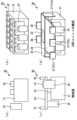
- FIG. 2 is a diagram showing an example of the configuration of the IGBT unit 30 shown in FIG. 1.
- FIG. 2(a) is a side view showing an example of the configuration of a portion of the IGBT unit 30.
- FIG. 2(b) is a perspective view showing an example of the configuration of a portion of the IGBT unit 30.
- FIG. 2(c) is a side view showing an example of the overall configuration of the IGBT unit 30.
- FIG. 2(d) is a perspective view showing an example of the overall configuration of the IGBT unit 30.
- the IGBT unit 30 has multiple DC capacitors 22, a cooler 31, and multiple semiconductors 32.
- the cooler 31 has a plurality of semiconductors 32 arranged in contact with its upper surface, and a plurality of DC capacitors 22 arranged adjacent to its front surface.
- the cooler 31 has, for example, a plurality of fins arranged in the flow of the refrigerant and a fan for circulating the refrigerant, and transfers heat radiated from the plurality of semiconductor elements 32 to the refrigerant, thereby cooling the plurality of semiconductor elements 32 in contact with it and other elements within the IGBT unit 30.
- the multiple semiconductors (semiconductor elements) 32 are arranged so as to abut against one surface of the cooler 31.
- the multiple semiconductors 32 are, for example, multiple switching elements such as IGBTs, and convert DC power into AC power according to control by gate signals from a control device 40 (control board 41) via a gate driver board 33 described below.
- the IGBT unit 30 further includes a gate driver board 33, a main circuit conductor 34, a support member 35, a DC terminal 36, and an AC terminal 37.
- the gate driver board 33 is disposed on top of a support member 35 disposed on the upper surface of the multiple semiconductors 32 in Figs. 2(c) and (d).
- the gate driver board 33 transmits gate signals output from a control device 40 (control board 41) to the gates of the multiple semiconductors (semiconductor elements) 32 to control the semiconductors 32.
- the main circuit conductor 34 (laminated bus bar) is disposed above the DC capacitor 22 and the semiconductor 32 in Figs. 2(c) and (d), with a DC terminal 36 provided on the cooler 31 side and an AC terminal 37 provided on the DC capacitor 22 side.
- the main circuit conductor 34 is, for example, a laminated bus bar in which multiple conductive layers and insulating layers are laminated in a predetermined arrangement from the DC terminal 36 to the AC terminal 37.
- the support member 35 is supported by the cooler 31 and is disposed above the main circuit conductor 34, and the gate driver board 33 is disposed above the support member 35.
- the DC terminal 36 is provided on the cooler 31 side of the main circuit conductor 34 in Figures 2(c) and (d), and is connected to the DC bus 5 outside the IGBT unit 30 (see Figure 1, etc.).
- the AC terminal 37 is provided on the DC capacitor 22 side of the main circuit conductor 34, and is connected to the AC circuit 6 outside the IGBT unit 30 (see FIG. 1, etc.). As described below, the AC terminal 37 has three terminals, AC terminal 37a, AC terminal 37b, and AC terminal 37c (see FIG. 9, etc.). Note that AC terminal 37a is an example of a "first AC terminal”, AC terminal 37b is an example of a "second AC terminal”, and AC terminal 37c is an example of a "third AC terminal”.
- FIG. 3 is a diagram showing an example of the arrangement of each component inside the housing 11 of the power conversion device 10 shown in FIG. 1.
- FIG. 3(a) is a front view showing an example of the arrangement of each component inside the housing 11 of the power conversion device 10 shown in FIG. 1.
- FIG. 3(b) is a side view showing an example of the arrangement of each component inside the housing 11 of the power conversion device 10 shown in FIG. 1.
- FIG. 3(c) is a rear view showing an example of the arrangement of each component inside the housing 11 of the power conversion device 10 shown in FIG. 1.
- FIG. 3(b) is a right side view of FIG. 3(a).
- the power conversion device 10 has, inside the housing 11, an air intake 12 in the upper section, a DC circuit breaker 21 in the middle left section, an AC circuit breaker 25 in the middle right section, a DC input unit 5a in the lower left section, and a control board 41, etc. in the lower right section when viewed from the front.
- the power conversion device 10 has an AC circuit breaker 25 in the middle front section in a side view, and a control board 41 and the like in a lower front section.
- the power conversion device 10 has an air intake 12 in the upper center section in a side view, an IGBT unit 30 in the middle center section, and an AC reactor 24a in the lower center section.
- the power conversion device 10 has a fan 13 in the lower rear section in a side view.
- the power conversion device 10 has an intake port 12 in the upper stage when viewed from the rear, an IGBT unit 30 on each side of the middle stage, and a fan 13 on each side of the lower stage.
- the two IGBT units 30 arranged on each side have the same structure from the viewpoint of manufacturability, etc.
- control board 41 etc. implements the main control board 42 and the signal distribution board 43 described below (see Figure 6 etc.).
- FIG. 4 is a side view showing an example of the division between a semiconductor cooling area A and an electronic component area B in the layout structure inside the housing 11 of the power conversion device 10 shown in FIG. 3.
- FIG. 4(a) is a side view showing an example of the semiconductor cooling area A in the layout structure inside the housing 11 of the power conversion device 10 shown in FIG. 3.
- FIG. 4(b) is a side view showing an example of the electronic component area B in the layout structure inside the housing 11 of the power conversion device 10 shown in FIG. 3. Note that, like FIG. 3(b), FIGS. 4(a) and (b) are right side views of FIG. 3(a).
- the semiconductor cooling area A is, for example, the area on the outside left and right of the IGBT unit 30 and the AC reactor 24a when viewed from the front and rear, and outside air is taken in through the intake port 12 and expelled from the fan 13 (see FIG. 5, etc.).
- the air intake 12 is made of, for example, punched sheet metal, and actively takes in outside air to cool the semiconductors 32 (for the cooler 31 that cools the semiconductors 32).
- the semiconductor cooling area A is an area where improving cooling performance is more important than reducing the risk of contamination by outside air.
- the cooler 31 of the IGBT unit 30, for which improving cooling performance is more important than reducing the risk of contamination by outside air, is placed in the semiconductor cooling area A (see Figure 5, etc.).
- the air intake 12 is an example of a "first air intake".
- Fan (cooling fan) 13 is provided on the rear side of the lower part of the housing 11. As shown by the arrows indicating the air flow in FIG. 4(a), outside air is taken in through the air intake 12, passes through the semiconductor cooling area A, and is exhausted from fan (cooling fan) 13.
- electronic component area B is, for example, the inner area when viewed from the front and rear (see FIG. 5, etc.), and air is taken in from an air intake 14 dedicated to electronic component area B provided on the front side of the housing 11.
- air intake 14 dedicated to electronic component area B provided on the front side of the housing 11.
- the air intake 14 has, for example, an air filter 14a, and takes in clean air through the air filter 14a.
- the electronic component area B is an area where minimizing the risk of contamination by outside air is more important than improving cooling performance.
- the semiconductor 32 and gate driver board 33 of the IGBT unit 30, which need to be isolated from the outside air that poses the risk of contamination, are arranged facing each other (see Figure 5, etc.).
- the air intake 14 is an example of a "second air intake".
- the IGBT unit 30 is designed in advance so that the areas are physically separated, for example, by partitions or sheet metal of the cooler 31, so that the semiconductors 32 and gate driver board 33 are not exposed to the outside air.
- the semiconductor cooling area A and the electronic component area B are designed so that they have different intake parts, intake port 12 and intake port 14, and are structurally separated inside the housing 11.
- clean air taken in from air intake 14 passes through electronic component area B and is exhausted from fan (cooling fan) 13. That is, in this embodiment, the exhaust section is common to semiconductor cooling area A and electronic component area B, and the outside air that has flowed through semiconductor cooling area A and the clean air that has flowed through electronic component area B join together and are exhausted from the same fan 13.
- the outside air that has flowed through semiconductor cooling area A and the clean air that has flowed through electronic component area B may be exhausted separately without joining together.
- FIG. 5 is a rear view showing an example of the division of the semiconductor cooling area A and the electronic component area B in the layout structure inside the housing 11 of the power conversion device 10 shown in FIG. 3.
- the housing (panel) 11 of the power conversion device 10 has an air intake 12 in the upper section when viewed from the rear, an IGBT unit 30 on each of the left and right sides of the middle section, and a fan (cooling fan) 13 on each of the left and right sides of the lower section.
- the outer left and right sides are semiconductor cooling area A
- the inner side is electronic component area B.
- the two IGBT units 30 on the left and right sides have the same structure from the standpoint of manufacturability, etc.
- the semiconductor cooling area A is an area where outside air is actively taken in from the air intake 12, and the cooler 31 and AC reactor 24a, which are parts of the IGBT unit 30 that do not need to be isolated from the outside air that may be at risk of contamination, are arranged in this area.
- the cooler 31 is arranged on the outside of the left and right sides of the IGBT unit 30.
- the outside of the IGBT unit 30 and AC reactor 24a in the power conversion device 10 (housing 11) can be divided into a semiconductor cooling area A, and the inside into an electronic component area B.
- This improves environmental resistance by arranging the semiconductor 32 and gate driver board 33, which are at risk of contamination and need to be isolated from the outside air, facing each other in the electronic component area B.
- the cooling flow path for the IGBT unit 30 is simplified, making it possible to create a layout with less pressure loss.
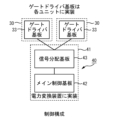
- FIGS. 6 and 7 are diagrams showing an example of the control configuration of the power conversion device 10 shown in FIGS. 1 to 5.
- the control board 41 in the control device 40 has a main control board 42 and a signal distribution board 43.
- each IGBT unit 30 arranged on the left and right sides of the housing 11 of the power conversion device 10 when viewed from the front and back has a gate driver board 33.
- the main control board 42 is the board that actually performs the control, and generates and outputs gate signals that turn on and off the gates of the semiconductors (semiconductor elements) 32 of the IGBT units 30.
- the signal distribution board 43 is a board that rearranges (distributes) the wiring in order to transmit the signal output from the main control board 42 to each gate driver board 33.
- the signal distribution board 43 divides (distributes) the signal output from the main control board 42 and outputs it to each gate driver board 33.
- the gate driver board 33 is a board that transmits electrical signals output from the control board 41 to the gates of multiple semiconductors (semiconductor elements) 32 after isolating them with, for example, a photocoupler, thereby controlling the semiconductors 32 (see Figure 2, etc.).
- the IGBT unit 30 converts the DC power supplied from the DC terminal 36 into AC power based on the gate signal output from the main control board 42 and distributed by the signal distribution board 43 to each gate driver board 33, and outputs it from the AC terminal 37. At this time, as shown in FIG. 7, the DC power is branched into two and supplied to the two IGBT units 30, and the AC powers converted and output by the two IGBT units 30 are output from the two IGBT units 30 and then merged into one.
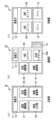
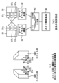
- FIG. 8 is a diagram showing an example of the arrangement of the IGBT units 30 in the power conversion device 10 and the control configuration of a conventional signal distribution board 43'.
- FIG. 8(a) is a diagram showing an example of the arrangement of the IGBT units 30 in the power conversion device 10.
- FIG. 8(b) is a diagram showing an example of the control configuration of a conventional signal distribution board 43' in the power conversion device 10.
- the semiconductor 32 and the gate driver board 33 are arranged facing each other in the electronic component area B (see Fig. 5, etc.).
- the two IGBT units 30 on the left and right sides have the same structure from the viewpoint of manufacturability, etc.
- the U phases must be connected to each other, the V phases must be connected to each other, and the W phases must be connected to each other.
- the signal distribution board 43' distributes a signal to two IGBT units 30, it sends the same signal to each of the AC terminals 37a to 37c of the two IGBT units 30.
- the signal distribution board 43' sends a U-phase signal to each of the AC terminals 37a of the two IGBT units 30, a V-phase signal to each of the AC terminals 37b, and a U-phase signal to each of the AC terminals 37a via the gate driver board 33.
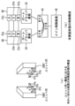
- FIG. 9 is a diagram showing an example of the arrangement of the IGBT units 30 in the power conversion device 10 according to the first embodiment and the control configuration of the signal distribution board 43.
- FIG. 9(a) is a diagram showing an example of the arrangement of the IGBT units 30 in the power conversion device 10 according to the first embodiment.
- FIG. 9(b) is a diagram showing an example of the control configuration of the signal distribution board 43 in the power conversion device 10 according to the first embodiment.
- the AC terminals 37a, 37b, 37c of one IGBT unit 30 are U-phase, V-phase, and W-phase, respectively, and the AC terminals 37a, 37b, 37c of the other IGBT unit 30 are W-phase, V-phase, and U-phase, respectively. Therefore, as shown in FIG. 9(a), even if two IGBT units 30 having the same structure are arranged facing each other from the viewpoint of manufacturability, etc., the U-phase AC terminal 37a and the U-phase AC terminal 37c are arranged facing each other.
- the V-phase AC terminal 37b and the V-phase AC terminal 37b are arranged facing each other, and similarly, the W-phase AC terminal 37c and the W-phase AC terminal 37a are arranged facing each other.
- the connections do not cross (intersect), and the U-phases, the V-phases, and the W-phases are connected to each other at the shortest distance.
- the signal distribution board 43 when the signal distribution board 43 according to this embodiment distributes signals to two IGBT units 30, it sends U-phase, V-phase, and W-phase signals to AC terminals 37a, 37b, and 37c, respectively, to one IGBT unit 30.
- the signal distribution board 43 switches the wiring so that the U-phase and W-phase signals are inverted, and sends W-phase, V-phase, and U-phase signals to AC terminals 37a, 37b, and 37c, respectively, to the other IGBT unit 30.
- the connections of the U-phase, V-phase, and W-phase do not become intertwined, and the connection distance of each conductor does not become long. Furthermore, because the U-phases, V-phases, and W-phases are connected at the shortest distance, the amount of conductors used can be reduced compared to conventional methods, and the conductor connections can be simplified and optimized.
- One IGBT unit 30 is an example of a "first three-phase integrated semiconductor unit,” and the other IGBT unit 30 is an example of a "second three-phase integrated semiconductor unit.”
- the outside of the power conversion device 10 (housing 11) is divided into a semiconductor cooling area A and the inside is divided into an electronic component area B, and the IGBT units 30 are arranged facing each other.
- the cooling flow path becomes simple, and a layout with less pressure loss can be achieved.
- the cooler 31 of the IGBT unit 30 is placed in the semiconductor cooling area A, where outside air is actively taken in and where improving cooling performance is more important than reducing the risk of contamination by outside air.
- the cooling performance of the semiconductor 32 is guaranteed even when two (multiple) IGBT units 30 are placed inside the housing 11.
- the semiconductor 32 and gate driver board 33 of the two (multiple) IGBT units 30 that need to be isolated from the outside air that may be contaminated are arranged facing each other in the electronic component area B.
- the semiconductor 32 and gate driver board 33 that need to be isolated from the outside air that may be contaminated are arranged in the electronic component area B, where clean air is taken in, although the air volume is less than that of the semiconductor cooling area A. Therefore, according to this embodiment, environmental resistance can be improved.
- the signal distribution board 43 when the signal distribution board 43 distributes signals to two (multiple) IGBT units 30, it sends U-phase, V-phase, and W-phase signals to AC terminals 37a, 37b, and 37c in that order to one IGBT unit 30.
- the signal distribution board 43 switches the wiring so that the U-phase and W-phase signals are inverted to send W-phase, V-phase, and U-phase signals to AC terminals 37a, 37b, and 37c in that order to the other IGBT unit 30.
- the control configuration of the signal distribution board 43 is changed, and the wiring of one of the opposing IGBT units 30 is not swapped, but the wiring of only the other IGBT unit 30 is swapped so that the U-phase and W-phase signals are inverted.
- the structure of the two IGBT units 30 can remain the same, thereby improving manufacturability and interchangeability.
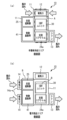
- FIG. 10 is a diagram showing an example of the arrangement of each component in the power conversion device 10A according to the second embodiment and the division between the semiconductor cooling area A and the electronic component area B.
- FIG. 10(a) is a side view showing an example of the arrangement of each component in the power conversion device 10A according to the second embodiment and the division between the semiconductor cooling area A and the electronic component area B.
- FIG. 10(b) is a rear view showing an example of the arrangement of each component in the power conversion device 10A according to the second embodiment and the division between the semiconductor cooling area A and the electronic component area B.
- the same reference numerals are used for the same or similar components as those in the first embodiment shown in FIGS. 1 to 7 and 9, and detailed description thereof will be omitted or simplified.
- an air intake 14 having an air filter 14a is provided on the front side of the housing 11 for use only with the electronic component area B (see Figure 4, etc.).
- clean air is taken in from the air intake 14 through the air filter 14a, passes through the electronic component area B, then merges with the outside air in the semiconductor cooling area A and is exhausted from a shared fan 13.
- a heat exchanger 15 is provided on the front side of the housing 11A instead of the air filter 14a, and a partition wall 16, for example, is disposed between the electronic component area B and the fan 13.
- the heat exchanger 15 absorbs heat from the clean air (internal air) that has been heated by heat radiation from the semiconductors 32 and other components in the electronic component area B, and cools it.
- the partition wall 16 is, for example, a metal plate, and blocks the exhaust section on the electronic component area B side inside the housing (panel) 11A (between electronic component area B and the fan 13). Note that what blocks the exhaust section on the electronic component area B side is not limited to the partition wall 16.
- the power conversion device 10A (housing 11) may originally have a structure in which the exhaust section on the electronic component area B side is blocked.
- the second embodiment shown in FIG. 10 has the same effects as the first embodiment shown in FIGS. 1 to 7 and 9.
- the inside and outside air can be completely separated, so the electronic component area B can be kept cleaner than in the first embodiment, and environmental resistance can be improved.
- FIG. 11 is a diagram showing an example of an arrangement structure of the IGBT units 30 in a power conversion device 10B according to the third embodiment.
- the same or similar configurations as those in the first embodiment shown in Figs. 1 to 7 and 9 are denoted by the same reference numerals, and detailed description thereof will be omitted or simplified.
- the IGBT units 30 are arranged inside the housing 11B.
- the IGBT units 30 are arranged facing each other, with pairs of two IGBT units 30 arranged facing each other being arranged above and below.
- the U-phases, V-phases, and W-phases of the pairs of IGBT units 30 arranged facing each other are connected at the shortest distance on the opposing fronts, and further the upper and lower U-phases, V-phases, and W-phases are connected in the vertical direction, respectively.
- the signal distribution board 43 has the same configuration as in the first embodiment, so the control configuration of the signal distribution board 43 has been changed.
- the wiring of one of the IGBT units 30 arranged opposite each other is not swapped by the signal distribution board 43, and the wiring of the other IGBT unit 30 is swapped by the signal distribution board 43 so that the U-phase and W-phase signals are inverted by the signal distribution board 43.
- the U-phases, V-phases, and W-phases of the IGBT units 30 arranged opposite each other are connected at the shortest distance on the opposing front sides, and further the upper and lower U-phases, V-phases, and W-phases can be connected vertically.
- the number of IGBT units 30 in the third embodiment is not limited to four, and may be any even number, such as six.
- pairs of two IGBT units 30 arranged facing each other are arranged two by two in the vertical direction.
- the conductors of the U-phases, V-phases, and W-phases of the IGBT units 30 arranged in the vertical direction are connected face-to-face in the horizontal direction, and are then further connected in the vertical direction.
- the U-phase and W-phase of one IGBT unit 30 can be inverted to facilitate connection of the conductors of the phases facing each other, as well as connection of the conductors of the phases above and below.
- Fig. 12 is a diagram showing an example of an arrangement of the IGBT units 130 in the power conversion device 110 according to the first comparative example.
- Fig. 12(a) is a perspective view showing an example of an arrangement of the IGBT units 130 in the power conversion device 110 according to the first comparative example.
- Fig. 12(b) is a side view showing an example of an arrangement of the IGBT units 130 in the power conversion device 110 according to the first comparative example.
- the power conversion device 110 according to the first comparative example is, for example, an outdoor unit of a side-by-side panel model, and as shown in Figs. 12(a) and (b), one IGBT unit 130 is arranged for one panel (housing) 111, and a fan 113 is arranged below the IGBT unit 130.
- the number of semiconductor elements such as IGBTs has been increasing with the expansion of inverter capacity, and there is a need to arrange multiple IGBT units 130 for one panel 111.
- Fig. 13 is a diagram showing an example of an arrangement of the IGBT units 230 in the power conversion device 210 according to the second comparative example.
- Fig. 13(a) is a perspective view showing an example of an arrangement of the IGBT units 230 in the power conversion device 210 according to the second comparative example.
- Fig. 13(b) is a side view showing an example of an arrangement of the IGBT units 230 in the power conversion device 210 according to the second comparative example.
- the power conversion device 210 is, for example, an indoor unit, and a plurality of IGBT units 230 are arranged in a multi-layered manner on a single board (housing) 211, like a server rack.
- a plurality of fans 213 must be arranged in a single board 211 in a horizontal direction with the IGBT units 230 according to the number of IGBT units 230. This is because, for example, when the fan 213 is arranged at the bottom, as in the first comparative example shown in FIG. 12, the upper IGBT units 230 and the lower IGBT units 230 stacked in a multi-layered manner, like a server rack, cannot be uniformly cooled. For this reason, in the structure of the second comparative example shown in FIG. 13, a large number of fans 213 are used when attempting to uniformly cool a plurality of IGBT units 230.
- FIG. 14 is a diagram showing an example of an arrangement structure of IGBT units 330 in a power conversion device 310 according to a third comparative example.
- multiple IGBT units 330 are arranged in multiple layers on a panel (housing) 311 like a server rack.
- electronic component area B where, for example, semiconductors 32 and gate driver boards 33 are arranged
- semiconductor cooling area A where, for example, coolers 31 are arranged.
- the electronic component area B when the areas are divided, the electronic component area B has a smaller air volume and is less susceptible to contamination from the outside air than the semiconductor cooling area A, so a structure as simple as possible is advantageous in terms of cooling with less pressure loss.
- the IGBT units 330 are stacked in a vertical line in multiple tiers as in the third comparative example, if the area is divided (separated into inside and outside air), the electronic component area B will have a complex structure because it is equipped with precision machinery such as the gate driver board 33.
- the IGBT units 30 are arranged facing each other, so the structure of the electronic component area B is simpler than that of the third comparative example shown in Figure 14, and pressure loss is reduced, allowing for efficient cooling.
- the first to third embodiments shown in Figures 1 to 7 and 9 to 11 while improving environmental resistance, ensuring cooling performance, simplifying the cooling flow path, and improving replaceability compared to the third comparative example, it is possible to reduce the amount of conductor used, simplify and optimize conductor connections.
- IGBT Three-phase integrated semiconductor unit
- IGBT Semiconductor element
- GAT Semiconductor element
- GAT Gate driver board
- PCS Power conversion system
- PCS Power conversion system
- Housing panel
- 113... Fan cooling fan
- PCS Power conversion system
Landscapes
- Engineering & Computer Science (AREA)
- Microelectronics & Electronic Packaging (AREA)
- Power Engineering (AREA)
- Physics & Mathematics (AREA)
- Thermal Sciences (AREA)
- Inverter Devices (AREA)
Abstract
Description
図1は、第1実施形態に係る電力変換装置10の構成の一例を示す図である。なお、本実施形態では、電力変換装置10が用いられる電力変換システムの一例として、直流電源が太陽光パネル2である太陽光発電システム1について説明する。しかし、これには限られず、本実施形態の電力変換装置10が用いられる電力変換システムは、例えば、直流電源が、蓄電池であっても、太陽電池と蓄電池とが組み合わされたものであってもよい。
以上、図1~図7及び図9に示す第1実施形態によれば、電力変換装置10(筐体11)の外側を半導体冷却エリアA、内側を電子部品エリアBとして区分けし、IGBTユニット30を向かい合わせに配置することとした。これにより、本実施形態によれば、2つの(複数の)IGBTユニット30が筐体11内に配置された場合であっても、冷却流路が単純になり、圧損の少ないレイアウトを可能にすることができる。
図10は、第2実施形態に係る電力変換装置10Aにおける各構成の配置構造及び半導体冷却エリアAと電子部品エリアBとの区分けの一例を示す図である。図10(a)は、第2実施形態に係る電力変換装置10Aにおける各構成の配置構造及び半導体冷却エリアAと電子部品エリアBとの区分けの一例を示す側面図である。図10(b)は、第2実施形態に係る電力変換装置10Aにおける各構成の配置構造及び半導体冷却エリアAと電子部品エリアBとの区分けの一例を示す背面図である。なお、図10において、図1~図7及び図9に示す第1実施形態の構成と同一又は同様の構成については同一の符号を付し、詳細な説明は省略又は簡略化する。
以上、図10に示す第2実施形態では、図1~図7及び図9に示す第1実施形態と同様の効果を有する。
図11は、第3実施形態に係る電力変換装置10BにおけるIGBTユニット30の配置構造の一例を示す図である。なお、図11において、図1~図7及び図9に示す第1実施形態の構成と同一又は同様の構成については同一の符号を付し、詳細な説明は省略又は簡略化する。
以上、図11に示す第3実施形態では、IGBTユニット30が筐体11B内に4台以上の偶数台配置された場合であっても、図1~図7及び図9に示す第1実施形態と同様の効果を有する。
図12は、第1比較例に係る電力変換装置110におけるIGBTユニット130の配置構造の一例を示す図である。図12(a)は、第1比較例に係る電力変換装置110におけるIGBTユニット130の配置構造の一例を示す斜視図である。図12(b)は、第1比較例に係る電力変換装置110におけるIGBTユニット130の配置構造の一例を示す側面図である。
図13は、第2比較例に係る電力変換装置210におけるIGBTユニット230の配置構造の一例を示す図である。図13(a)は、第2比較例に係る電力変換装置210におけるIGBTユニット230の配置構造の一例を示す斜視図である。図13(b)は、第2比較例に係る電力変換装置210におけるIGBTユニット230の配置構造の一例を示す側面図である。
図14は、第3比較例に係る電力変換装置310におけるIGBTユニット330の配置構造の一例を示す図である。
以上、図1~図7及び図9~図11に示す第1~第3実施形態によれば、図1~図7及び図9に示す第1実施形態と、図10に示す第2実施形態と、図11に示す第3実施形態とに分かれているが、これらの実施形態が直列に又は並列に組み合わされてもよい。組み合わされた実施形態もまた、組み合わされる前の各実施形態が奏する各作用効果と同様の作用効果を奏することができる。
Claims (5)
- 筐体と、前記筐体内にそれぞれ同一構造の第1の三相一括半導体ユニットと第2の三相一括半導体ユニットと、を備える電力変換装置であって、
前記第1の三相一括半導体ユニットと前記第2の三相一括半導体ユニットとは、
それぞれ冷却器と、半導体と、ゲートドライバ基板と、第1交流端子と、第2交流端子と、第3交流端子とを有し、
それぞれ前記筐体内の外側に前記冷却器が配され、前記筐体内の内側に前記半導体と、前記ゲートドライバ基板と、前記第1交流端子と、前記第2交流端子と、前記第3交流端子とが配されるように、前記筐体内で、前記第1交流端子と、前記第2交流端子と、前記第3交流端子とが向かい合わせに配置され、
前記第1の三相一括半導体ユニットは、前記電力変換装置が有する信号分配基板によって、前記第1交流端子にはU相の信号が送信され、前記第2交流端子にはV相の信号が送信され、前記第3交流端子にはW相の信号が送信されるよう構成され、
前記第2の三相一括半導体ユニットは、前記電力変換装置が有する前記信号分配基板によって、U相とW相とが反転するように配線が入れ替えられ、前記第1交流端子にはW相の信号が送信され、前記第2交流端子にはV相の信号が送信され、前記第3交流端子にはU相の信号が送信されるよう構成される
ことを特徴とする電力変換装置。 - 請求項1に記載の電力変換装置において、
前記信号分配基板によって、それぞれ前記U相の信号が送信される前記第1の三相一括半導体ユニットの前記第1交流端子と、前記第2の三相一括半導体ユニットの前記第3交流端子とは、前記筐体内の内側で向かい合わせに正面で接続され、
前記信号分配基板によって、それぞれ前記V相の信号が送信される前記第1の三相一括半導体ユニットの前記第2交流端子と、前記第2の三相一括半導体ユニットの前記第2交流端子とは、前記筐体内の内側で向かい合わせに正面で接続され、
前記信号分配基板によって、それぞれ前記W相の信号が送信される前記第1の三相一括半導体ユニットの前記第3交流端子と、前記第2の三相一括半導体ユニットの前記第1交流端子とは、前記筐体内の内側で向かい合わせに正面で接続される
ことを特徴とする電力変換装置。 - 請求項1に記載の電力変換装置において、
前記筐体は、
前記筐体内の外側の半導体冷却エリアを冷却する外気を取り入れる第1吸気口と、
前記筐体内の内側の電子部品エリアを冷却するクリーンな空気を、エアフィルタを介して取り入れる第2吸気口と、
冷却ファンと、
を備え、
前記半導体冷却エリアには前記第1吸気口から取り入れられた前記外気のみが流れ、前記電子部品エリアには前記エアフィルタを介して前記第2吸気口から取り入れられた前記クリーンな空気のみが流れるよう、前記半導体冷却エリアと前記電子部品エリアとは、前記筐体内で分離されており、
前記冷却ファンは、前記筐体内を別々に流れた後に合流した前記外気と前記クリーンな空気とを排気するよう構成される
ことを特徴とする電力変換装置。 - 請求項1に記載の電力変換装置において、
前記筐体は、
前記筐体内の外側の半導体冷却エリアを冷却する外気を取り入れる第1吸気口と、
前記筐体内の内側の電子部品エリアを冷却する内気の熱を吸熱する熱交換器と、
冷却ファンと、
を備え、
前記半導体冷却エリアには前記第1吸気口から取り入れられた前記外気のみが流れ、前記電子部品エリアには前記熱交換器により吸熱されて冷却された前記内気のみが循環して流れるよう、前記半導体冷却エリアと前記電子部品エリアとは、前記筐体内で分離されており、
前記冷却ファンは、前記外気のみを排気するよう構成される
ことを特徴とする電力変換装置。 - 請求項2に記載の電力変換装置において、
前記筐体内には、前記第1の三相一括半導体ユニットと前記第2の三相一括半導体ユニットとの組が上下方向に複数配置され、
前記筐体内の内側で向かい合わせに正面で接続された複数組の前記第1の三相一括半導体ユニットの前記第1交流端子と、前記第2の三相一括半導体ユニットの前記第3交流端子とは、上下方向でさらに接続され、
前記筐体内の内側で向かい合わせに正面で接続された複数組の前記第1の三相一括半導体ユニットの前記第2交流端子と、前記第2の三相一括半導体ユニットの前記第2交流端子とは、上下方向でさらに接続され、
前記筐体内の内側で向かい合わせに正面で接続された複数組の前記第1の三相一括半導体ユニットの前記第3交流端子と、前記第2の三相一括半導体ユニットの前記第1交流端子とは、上下方向でさらに接続される
ことを特徴とする電力変換装置。
Priority Applications (3)
| Application Number | Priority Date | Filing Date | Title |
|---|---|---|---|
| JP2024525878A JP7622907B2 (ja) | 2022-10-31 | 2022-10-31 | 電力変換装置 |
| US18/709,086 US20250038672A1 (en) | 2022-10-31 | 2022-10-31 | Power conversion device |
| PCT/JP2022/040817 WO2024095348A1 (ja) | 2022-10-31 | 2022-10-31 | 電力変換装置 |
Applications Claiming Priority (1)
| Application Number | Priority Date | Filing Date | Title |
|---|---|---|---|
| PCT/JP2022/040817 WO2024095348A1 (ja) | 2022-10-31 | 2022-10-31 | 電力変換装置 |
Publications (1)
| Publication Number | Publication Date |
|---|---|
| WO2024095348A1 true WO2024095348A1 (ja) | 2024-05-10 |
Family
ID=90929967
Family Applications (1)
| Application Number | Title | Priority Date | Filing Date |
|---|---|---|---|
| PCT/JP2022/040817 Ceased WO2024095348A1 (ja) | 2022-10-31 | 2022-10-31 | 電力変換装置 |
Country Status (3)
| Country | Link |
|---|---|
| US (1) | US20250038672A1 (ja) |
| JP (1) | JP7622907B2 (ja) |
| WO (1) | WO2024095348A1 (ja) |
Citations (5)
| Publication number | Priority date | Publication date | Assignee | Title |
|---|---|---|---|---|
| US20150138689A1 (en) * | 2011-08-15 | 2015-05-21 | Lear Corporation | Power Module Cooling System |
| JP2017522843A (ja) * | 2014-06-20 | 2017-08-10 | ゼネラル・エレクトリック・カンパニイ | マルチインバータ電力変換器の制御装置および方法 |
| JP2018133864A (ja) * | 2017-02-14 | 2018-08-23 | 株式会社明電舎 | 単相インバータの出力側接続構造 |
| JP2020014380A (ja) * | 2019-09-26 | 2020-01-23 | 日立オートモティブシステムズ株式会社 | 電動駆動装置 |
| US20220190736A1 (en) * | 2020-12-15 | 2022-06-16 | Caterpillar Inc. | Modular configurable inverter and systems, components, and methods thereof |
Family Cites Families (1)
| Publication number | Priority date | Publication date | Assignee | Title |
|---|---|---|---|---|
| WO2019207723A1 (ja) * | 2018-04-26 | 2019-10-31 | 東芝三菱電機産業システム株式会社 | 電力変換装置および電力変換ユニット |
-
2022
- 2022-10-31 US US18/709,086 patent/US20250038672A1/en active Pending
- 2022-10-31 WO PCT/JP2022/040817 patent/WO2024095348A1/ja not_active Ceased
- 2022-10-31 JP JP2024525878A patent/JP7622907B2/ja active Active
Patent Citations (5)
| Publication number | Priority date | Publication date | Assignee | Title |
|---|---|---|---|---|
| US20150138689A1 (en) * | 2011-08-15 | 2015-05-21 | Lear Corporation | Power Module Cooling System |
| JP2017522843A (ja) * | 2014-06-20 | 2017-08-10 | ゼネラル・エレクトリック・カンパニイ | マルチインバータ電力変換器の制御装置および方法 |
| JP2018133864A (ja) * | 2017-02-14 | 2018-08-23 | 株式会社明電舎 | 単相インバータの出力側接続構造 |
| JP2020014380A (ja) * | 2019-09-26 | 2020-01-23 | 日立オートモティブシステムズ株式会社 | 電動駆動装置 |
| US20220190736A1 (en) * | 2020-12-15 | 2022-06-16 | Caterpillar Inc. | Modular configurable inverter and systems, components, and methods thereof |
Also Published As
| Publication number | Publication date |
|---|---|
| JP7622907B2 (ja) | 2025-01-28 |
| US20250038672A1 (en) | 2025-01-30 |
| JPWO2024095348A1 (ja) | 2024-05-10 |
Similar Documents
| Publication | Publication Date | Title |
|---|---|---|
| US7881086B2 (en) | Power conversion device and fabricating method for the same | |
| US6822850B2 (en) | Laminated bus bar for use with a power conversion configuration | |
| US6885553B2 (en) | Bus bar assembly for use with a compact power conversion assembly | |
| JP5407275B2 (ja) | 電力変換装置 | |
| JP6429721B2 (ja) | 電力変換装置及び鉄道車両 | |
| US8576528B2 (en) | Matrix converter | |
| JP6296888B2 (ja) | 電力変換装置 | |
| CN106130363B (zh) | 电力变换装置以及铁道车辆 | |
| US20120020021A1 (en) | Matrix converter | |
| JP2008294067A (ja) | 半導体モジュール及びインバータ装置 | |
| US6956742B2 (en) | Compact liquid converter assembly | |
| CA2619956C (en) | Packaging system for modular power cells | |
| CN113632364B (zh) | 电力变换单元 | |
| CN108988655B (zh) | 电力电子控制器和电动汽车 | |
| JP2011109740A (ja) | 電力変換装置 | |
| JP5712750B2 (ja) | 電力変換装置 | |
| JP2019221048A (ja) | 電力変換装置 | |
| US20240324152A1 (en) | Cooling Apparatus | |
| JP7622907B2 (ja) | 電力変換装置 | |
| JP2022145741A (ja) | 無停電電源装置用制御装置 | |
| JP7771523B2 (ja) | 電力変換装置 | |
| JP7196877B2 (ja) | 電力変換装置 | |
| WO2025229734A1 (ja) | 電力変換装置および電気設備 | |
| JP7078182B2 (ja) | 電力変換器および電気自動車 | |
| CN209709697U (zh) | 光伏并网逆变器及其交流柜 |
Legal Events
| Date | Code | Title | Description |
|---|---|---|---|
| WWE | Wipo information: entry into national phase |
Ref document number: 202417034391 Country of ref document: IN |
|
| ENP | Entry into the national phase |
Ref document number: 2024525878 Country of ref document: JP Kind code of ref document: A |
|
| WWE | Wipo information: entry into national phase |
Ref document number: 18709086 Country of ref document: US |
|
| 121 | Ep: the epo has been informed by wipo that ep was designated in this application |
Ref document number: 22964370 Country of ref document: EP Kind code of ref document: A1 |
|
| NENP | Non-entry into the national phase |
Ref country code: DE |
|
| 122 | Ep: pct application non-entry in european phase |
Ref document number: 22964370 Country of ref document: EP Kind code of ref document: A1 |