WO2024090049A1 - 照明装置とその駆動方法 - Google Patents
照明装置とその駆動方法 Download PDFInfo
- Publication number
- WO2024090049A1 WO2024090049A1 PCT/JP2023/032665 JP2023032665W WO2024090049A1 WO 2024090049 A1 WO2024090049 A1 WO 2024090049A1 JP 2023032665 W JP2023032665 W JP 2023032665W WO 2024090049 A1 WO2024090049 A1 WO 2024090049A1
- Authority
- WO
- WIPO (PCT)
- Prior art keywords
- electrodes
- liquid crystal
- input signal
- circuit
- signal
- Prior art date
- Legal status (The legal status is an assumption and is not a legal conclusion. Google has not performed a legal analysis and makes no representation as to the accuracy of the status listed.)
- Ceased
Links
Images






Classifications
-
- G—PHYSICS
- G02—OPTICS
- G02F—OPTICAL DEVICES OR ARRANGEMENTS FOR THE CONTROL OF LIGHT BY MODIFICATION OF THE OPTICAL PROPERTIES OF THE MEDIA OF THE ELEMENTS INVOLVED THEREIN; NON-LINEAR OPTICS; FREQUENCY-CHANGING OF LIGHT; OPTICAL LOGIC ELEMENTS; OPTICAL ANALOGUE/DIGITAL CONVERTERS
- G02F1/00—Devices or arrangements for the control of the intensity, colour, phase, polarisation or direction of light arriving from an independent light source, e.g. switching, gating or modulating; Non-linear optics
- G02F1/01—Devices or arrangements for the control of the intensity, colour, phase, polarisation or direction of light arriving from an independent light source, e.g. switching, gating or modulating; Non-linear optics for the control of the intensity, phase, polarisation or colour
- G02F1/13—Devices or arrangements for the control of the intensity, colour, phase, polarisation or direction of light arriving from an independent light source, e.g. switching, gating or modulating; Non-linear optics for the control of the intensity, phase, polarisation or colour based on liquid crystals, e.g. single liquid crystal display cells
- G02F1/133—Constructional arrangements; Operation of liquid crystal cells; Circuit arrangements
- G02F1/1333—Constructional arrangements; Manufacturing methods
- G02F1/1347—Arrangement of liquid crystal layers or cells in which the final condition of one light beam is achieved by the addition of the effects of two or more layers or cells
-
- F—MECHANICAL ENGINEERING; LIGHTING; HEATING; WEAPONS; BLASTING
- F21—LIGHTING
- F21V—FUNCTIONAL FEATURES OR DETAILS OF LIGHTING DEVICES OR SYSTEMS THEREOF; STRUCTURAL COMBINATIONS OF LIGHTING DEVICES WITH OTHER ARTICLES, NOT OTHERWISE PROVIDED FOR
- F21V5/00—Refractors for light sources
-
- G—PHYSICS
- G02—OPTICS
- G02F—OPTICAL DEVICES OR ARRANGEMENTS FOR THE CONTROL OF LIGHT BY MODIFICATION OF THE OPTICAL PROPERTIES OF THE MEDIA OF THE ELEMENTS INVOLVED THEREIN; NON-LINEAR OPTICS; FREQUENCY-CHANGING OF LIGHT; OPTICAL LOGIC ELEMENTS; OPTICAL ANALOGUE/DIGITAL CONVERTERS
- G02F1/00—Devices or arrangements for the control of the intensity, colour, phase, polarisation or direction of light arriving from an independent light source, e.g. switching, gating or modulating; Non-linear optics
- G02F1/01—Devices or arrangements for the control of the intensity, colour, phase, polarisation or direction of light arriving from an independent light source, e.g. switching, gating or modulating; Non-linear optics for the control of the intensity, phase, polarisation or colour
- G02F1/13—Devices or arrangements for the control of the intensity, colour, phase, polarisation or direction of light arriving from an independent light source, e.g. switching, gating or modulating; Non-linear optics for the control of the intensity, phase, polarisation or colour based on liquid crystals, e.g. single liquid crystal display cells
-
- G—PHYSICS
- G02—OPTICS
- G02F—OPTICAL DEVICES OR ARRANGEMENTS FOR THE CONTROL OF LIGHT BY MODIFICATION OF THE OPTICAL PROPERTIES OF THE MEDIA OF THE ELEMENTS INVOLVED THEREIN; NON-LINEAR OPTICS; FREQUENCY-CHANGING OF LIGHT; OPTICAL LOGIC ELEMENTS; OPTICAL ANALOGUE/DIGITAL CONVERTERS
- G02F1/00—Devices or arrangements for the control of the intensity, colour, phase, polarisation or direction of light arriving from an independent light source, e.g. switching, gating or modulating; Non-linear optics
- G02F1/01—Devices or arrangements for the control of the intensity, colour, phase, polarisation or direction of light arriving from an independent light source, e.g. switching, gating or modulating; Non-linear optics for the control of the intensity, phase, polarisation or colour
- G02F1/13—Devices or arrangements for the control of the intensity, colour, phase, polarisation or direction of light arriving from an independent light source, e.g. switching, gating or modulating; Non-linear optics for the control of the intensity, phase, polarisation or colour based on liquid crystals, e.g. single liquid crystal display cells
- G02F1/133—Constructional arrangements; Operation of liquid crystal cells; Circuit arrangements
-
- G—PHYSICS
- G02—OPTICS
- G02F—OPTICAL DEVICES OR ARRANGEMENTS FOR THE CONTROL OF LIGHT BY MODIFICATION OF THE OPTICAL PROPERTIES OF THE MEDIA OF THE ELEMENTS INVOLVED THEREIN; NON-LINEAR OPTICS; FREQUENCY-CHANGING OF LIGHT; OPTICAL LOGIC ELEMENTS; OPTICAL ANALOGUE/DIGITAL CONVERTERS
- G02F1/00—Devices or arrangements for the control of the intensity, colour, phase, polarisation or direction of light arriving from an independent light source, e.g. switching, gating or modulating; Non-linear optics
- G02F1/01—Devices or arrangements for the control of the intensity, colour, phase, polarisation or direction of light arriving from an independent light source, e.g. switching, gating or modulating; Non-linear optics for the control of the intensity, phase, polarisation or colour
- G02F1/13—Devices or arrangements for the control of the intensity, colour, phase, polarisation or direction of light arriving from an independent light source, e.g. switching, gating or modulating; Non-linear optics for the control of the intensity, phase, polarisation or colour based on liquid crystals, e.g. single liquid crystal display cells
- G02F1/133—Constructional arrangements; Operation of liquid crystal cells; Circuit arrangements
- G02F1/13306—Circuit arrangements or driving methods for the control of single liquid crystal cells
-
- G—PHYSICS
- G02—OPTICS
- G02F—OPTICAL DEVICES OR ARRANGEMENTS FOR THE CONTROL OF LIGHT BY MODIFICATION OF THE OPTICAL PROPERTIES OF THE MEDIA OF THE ELEMENTS INVOLVED THEREIN; NON-LINEAR OPTICS; FREQUENCY-CHANGING OF LIGHT; OPTICAL LOGIC ELEMENTS; OPTICAL ANALOGUE/DIGITAL CONVERTERS
- G02F1/00—Devices or arrangements for the control of the intensity, colour, phase, polarisation or direction of light arriving from an independent light source, e.g. switching, gating or modulating; Non-linear optics
- G02F1/01—Devices or arrangements for the control of the intensity, colour, phase, polarisation or direction of light arriving from an independent light source, e.g. switching, gating or modulating; Non-linear optics for the control of the intensity, phase, polarisation or colour
- G02F1/13—Devices or arrangements for the control of the intensity, colour, phase, polarisation or direction of light arriving from an independent light source, e.g. switching, gating or modulating; Non-linear optics for the control of the intensity, phase, polarisation or colour based on liquid crystals, e.g. single liquid crystal display cells
- G02F1/133—Constructional arrangements; Operation of liquid crystal cells; Circuit arrangements
- G02F1/1333—Constructional arrangements; Manufacturing methods
- G02F1/1343—Electrodes
-
- G—PHYSICS
- G02—OPTICS
- G02F—OPTICAL DEVICES OR ARRANGEMENTS FOR THE CONTROL OF LIGHT BY MODIFICATION OF THE OPTICAL PROPERTIES OF THE MEDIA OF THE ELEMENTS INVOLVED THEREIN; NON-LINEAR OPTICS; FREQUENCY-CHANGING OF LIGHT; OPTICAL LOGIC ELEMENTS; OPTICAL ANALOGUE/DIGITAL CONVERTERS
- G02F1/00—Devices or arrangements for the control of the intensity, colour, phase, polarisation or direction of light arriving from an independent light source, e.g. switching, gating or modulating; Non-linear optics
- G02F1/01—Devices or arrangements for the control of the intensity, colour, phase, polarisation or direction of light arriving from an independent light source, e.g. switching, gating or modulating; Non-linear optics for the control of the intensity, phase, polarisation or colour
- G02F1/13—Devices or arrangements for the control of the intensity, colour, phase, polarisation or direction of light arriving from an independent light source, e.g. switching, gating or modulating; Non-linear optics for the control of the intensity, phase, polarisation or colour based on liquid crystals, e.g. single liquid crystal display cells
- G02F1/133—Constructional arrangements; Operation of liquid crystal cells; Circuit arrangements
- G02F1/1333—Constructional arrangements; Manufacturing methods
- G02F1/1343—Electrodes
- G02F1/134309—Electrodes characterised by their geometrical arrangement
-
- F—MECHANICAL ENGINEERING; LIGHTING; HEATING; WEAPONS; BLASTING
- F21—LIGHTING
- F21Y—INDEXING SCHEME ASSOCIATED WITH SUBCLASSES F21K, F21L, F21S and F21V, RELATING TO THE FORM OR THE KIND OF THE LIGHT SOURCES OR OF THE COLOUR OF THE LIGHT EMITTED
- F21Y2103/00—Elongate light sources, e.g. fluorescent tubes
-
- F—MECHANICAL ENGINEERING; LIGHTING; HEATING; WEAPONS; BLASTING
- F21—LIGHTING
- F21Y—INDEXING SCHEME ASSOCIATED WITH SUBCLASSES F21K, F21L, F21S and F21V, RELATING TO THE FORM OR THE KIND OF THE LIGHT SOURCES OR OF THE COLOUR OF THE LIGHT EMITTED
- F21Y2115/00—Light-generating elements of semiconductor light sources
- F21Y2115/10—Light-emitting diodes [LED]
Definitions
- One embodiment of the present invention relates to a lighting device and a driving method thereof.
- one embodiment of the present invention relates to a lighting device that uses the orientation of liquid crystals to control light distribution and a driving method thereof.
- An optical element known as a liquid crystal lens utilizes the fact that the refractive index of the liquid crystal layer changes as the orientation of the liquid crystal is controlled by controlling the voltage applied to the liquid crystal.
- An object of one embodiment of the present invention is to provide a lighting device having a new structure and a method for driving the same.
- an object of one embodiment of the present invention is to provide a lighting device capable of controlling light distribution based on an input signal of a pulse width modulation method and a method for driving the same.
- the lighting device includes a light source, an optical element, and a control device that drives the optical element.
- the optical element includes at least two liquid crystal cells that are arranged to transmit light emitted from the light source and overlap each other.
- Each of the at least two liquid crystal cells has a plurality of first electrodes and a plurality of second electrodes that are alternately arranged in stripes, a liquid crystal layer on the plurality of first electrodes and the plurality of second electrodes, and a plurality of third electrodes and a plurality of fourth electrodes that are arranged on the liquid crystal layer, intersect with the plurality of first electrodes and the plurality of second electrodes, and are alternately arranged in stripes.
- the control device is configured to receive a first input signal and a second input signal of a pulse width modulation type that specify the degree of diffusion of light by the optical element in the direction in which the plurality of first electrodes extend and the direction in which the plurality of third electrodes extend.
- the control device is further configured to convert the first input signal and the second input signal into a first output signal and a second output signal of a pulse amplitude type, respectively, according to a duty ratio, and supply them to the optical element.
- the lighting device includes a light source, an optical element, and a control device for controlling the optical element.
- the optical element includes at least two liquid crystal cells arranged to transmit light emitted from the light source and overlapping each other.
- Each of the at least two liquid crystal cells has a plurality of first electrodes and a plurality of second electrodes arranged alternately in stripes, a liquid crystal layer on the plurality of first electrodes and the plurality of second electrodes, and a plurality of third electrodes and a plurality of fourth electrodes arranged alternately in stripes on the liquid crystal layer, intersecting the plurality of first electrodes and the plurality of second electrodes.
- This driving method includes inputting a first input signal and a second input signal of a pulse width modulation type that specify the degree of diffusion of light by the optical element in the direction in which the plurality of first electrodes extend and the direction in which the plurality of third electrodes extend to the control device, and converting the first input signal and the second input signal into a first output signal and a second output signal of a pulse amplitude type, respectively, according to a duty ratio, and supplying them to the optical element.
- FIG. 1 is a schematic perspective view of an illumination device according to an embodiment of the present invention.
- 1 is a block diagram showing a configuration of a lighting device according to an embodiment of the present invention.
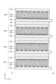
- 1 is a schematic end view of an illumination device according to one embodiment of the present invention;
- 1 is a schematic end view of an illumination device according to one embodiment of the present invention;
- FIG. 2 is a schematic plan view showing an electrode pattern of a liquid crystal cell included in an optical element of an illumination device according to an embodiment of the present invention.
- FIG. 2 is a schematic plan view showing an electrode pattern of a liquid crystal cell included in an optical element of an illumination device according to an embodiment of the present invention.
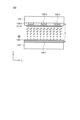
- FIG. 2 is a schematic end view illustrating diffusion of light by an optical element of an illumination device according to an embodiment of the present invention.
- FIG. 2 is a schematic end view illustrating diffusion of light by an optical element of an illumination device according to an embodiment of the present invention.
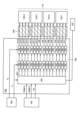
- FIG. 2 is a block diagram showing a configuration of a control device for a lighting device according to an embodiment of the present invention.
- 5A and 5B are schematic diagrams illustrating a method of driving a lighting device according to an embodiment of the present invention.
- 4 is a flowchart illustrating an example of a method for driving a lighting device according to an embodiment of the present invention.
- 4 is a flowchart illustrating an example of a method for driving a lighting device according to an embodiment of the present invention.
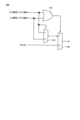
- 3 is an equivalent circuit diagram of a processing circuit included in a drive circuit of a lighting device according to an embodiment of the present invention.
- the term "on top” is used, unless otherwise specified, to include both a case in which another structure is placed directly on top of a structure so as to be in contact with the structure, and a case in which another structure is placed above a structure via yet another structure.
- two structures are "orthogonal” includes not only a state in which the two structures intersect perpendicularly (90°), but also a state in which the structures intersect at an angle of 90° ⁇ 10°.
- the following describes a lighting device 100 according to one embodiment of the present invention and a method for driving the same.
- Fig. 1 is a schematic perspective view showing the configuration of an illumination device 100 according to one embodiment of the present invention.
- the illumination device 100 includes an optical element 110, a light source 102, and a control device (not shown in Fig. 1).
- the illumination device 100 may further include an input device (not shown in Fig. 1) for outputting a signal for controlling the optical element 110 and inputting it to the control device 150.
- the input device may further be configured to be able to control the light intensity of the light source 102 via the control device or directly.
- the light source 102 is configured and arranged to emit light to the optical element 110.
- the light emitting elements included in the light source 102 include light emitting diodes (LEDs) and cold cathode fluorescent lamps.
- the optical element 110 is disposed on the light source 102 so as to transmit the light emitted by the light source 102.
- the optical element 110 includes at least two liquid crystal cells 120 that overlap each other on the light source 102.
- the number of liquid crystal cells 120 included in the optical element 110 may be three or more, and in the optical element 110 shown in FIG. 1, four liquid crystal cells (first liquid crystal cell 120-1, second liquid crystal cell 120-2, third liquid crystal cell 120-3, and fourth liquid crystal cell 120-4) are disposed on the light source 102 in order from the side closest to the light source 102.
- an illumination device 100 having an optical element 110 including four liquid crystal cells 120 will be used as an example.
- the direction from the light source 102 to the optical element 110 is defined as the z direction.
- Light emitted from the light source 102 is incident on the first liquid crystal cell 120-1 and is emitted from the fourth liquid crystal cell 120-4.
- the diffusion of light is controlled by the liquid crystal cell 120 contained in the optical element 110, and the light distribution of the light emitted from the optical element 110 can be changed.
- the light from the light source 102 can be processed to change the shape of the surface (illumination surface) on which the light illuminates an object.
- FIG. 2 shows a block diagram illustrating the configuration of the lighting device 100.
- each liquid crystal cell 120 is connected to a connector 108 such as a flexible printed circuit (FPC) board, and is connected to a control device 150 via the connector 108.
- FPC flexible printed circuit
- the control device 150 may be configured to be connected to the light source 102 and control the light source 102, or, although not shown, the light source 102 may be directly controlled by the input device 104 as described above.
- the control device 150 and the optical element 110 will be described in detail below.
- each of the first liquid crystal cell 120-1 to the fourth liquid crystal cell 120-4 includes a first substrate 122 and a second substrate 124 facing each other, and a plurality of first electrodes 126-1, a plurality of second electrodes 126-2, a plurality of third electrodes 126-3, a plurality of fourth electrodes 126-4, a first alignment film 128-1, and a second alignment film 128-2 are provided between them.
- the plurality of first electrodes 126-1 and the plurality of second electrodes 126-2 are provided on the first substrate 122, and a first alignment film 128-1 is formed on these electrodes.
- the plurality of third electrodes 126-3 and the plurality of fourth electrodes 126-4 are provided under the second substrate 124 and are disposed between the second substrate 124 and the second alignment film 128-2.
- the first substrate 122 and the second substrate 124 are fixed to each other by a sealant 132, and the liquid crystal layer 130 is sealed in a space surrounded by the first substrate 122, the second substrate 124, and the sealant 132.
- An adhesive 134 that transmits visible light is provided between the adjacent liquid crystal cells 120, thereby fixing the adjacent liquid crystal cells 120 to each other.
- an acrylic resin adhesive or an epoxy resin adhesive can be used as the adhesive 134.
- the first substrate 122 and the second substrate 124 are configured to transmit at least visible light of the light emitted by the light source 102.
- a light-transmitting substrate such as a glass substrate or a quartz substrate is used as the first substrate 122 and the second substrate 124.
- the first substrate 122 and the second substrate 124 may contain a light-transmitting polymer such as polyimide, polyamide, polycarbonate, acrylic resin, or polysiloxane.
- the multiple liquid crystal cells 120 are preferably arranged on the light source 102 such that the normal of the first substrate 122 and the second substrate 124 is the z direction and the main surface is the xy plane.
- Electrode Each of the electrodes 126 functions as an electrode for forming a transverse electric field in the liquid crystal layer 130.
- the electrodes 126 are made of a conductive oxide that transmits visible light, such as indium tin oxide (ITO) or indium zinc oxide (IZO).
- the electrodes 126 may contain a metal such as aluminum, tantalum, molybdenum, or tungsten, or an alloy thereof, but in order to ensure transparency to visible light, it is preferable to form the electrodes 126 in a mesh shape having a plurality of openings.
- the first electrodes 126-1 and the second electrodes 126-2 are arranged in stripes, parallel to each other, and alternately arranged. Therefore, one second electrode 126-2 is arranged between adjacent first electrodes 126-1, and one first electrode 126-1 is arranged between adjacent second electrodes 126-2.
- the third electrodes 126-3 and the fourth electrodes 126-4 are also arranged in stripes, parallel to each other, and alternately arranged. Therefore, one fourth electrode 126-4 is arranged between adjacent third electrodes 126-3, and one third electrode 126-3 is arranged between adjacent fourth electrodes 126-4.
- the direction in which the first electrode 126-1 and the second electrode 126-2 extend intersects or is perpendicular to the direction in which the third electrode 126-3 and the fourth electrode 126-4 extend.
- the extension directions of the first electrode 126-1 and the second electrode 126-2 are the same as each other, and the extension directions of the third electrode 126-3 and the fourth electrode 126-4 are also the same as each other. These relationships are also the same between the third liquid crystal cell 120-3 and the fourth liquid crystal cell 120-4.
- the extension directions of the first electrode 126-1 (or the second electrode 126-2) are perpendicular to each other, and the extension directions of the third electrode 126-3 (or the fourth electrode 126-4) are also perpendicular to each other.
- the optical element 110 when the optical element 110 is composed of two liquid crystal cells 120, the optical element 110 may be configured so that the extension directions of the first electrodes 126-1 (or second electrodes 126-2) between these liquid crystal cells 120 are the same, and the extension directions of the third electrodes 126-3 (or fourth electrodes 126-4) are also the same.
- the direction in which the first electrodes 126-1 and second electrodes 126-2 of the first liquid crystal cell 120-1 extend is defined as the y direction
- the direction in which the third electrodes 126-3 and fourth electrodes 126-4 extend is defined as the x direction.
- FIG. 5 and FIG. 6 are schematic plan views showing the patterns of the electrodes 126 formed on the first substrate 122 and the second substrate 124 of the liquid crystal cell 120, respectively.
- a plurality of first electrodes 126-1 and a plurality of second electrodes 126-2 arranged in a stripe pattern are provided on the first substrate 122.
- the plurality of first electrodes 126-1 are electrically connected to each other to form a comb-shaped pattern.
- the plurality of second electrodes 126-2 are also electrically connected to each other to form a comb-shaped pattern.
- the comb-shaped pattern of the first electrodes 126-1 and the second electrodes 126-2 extends to one side of the first substrate 122 and is electrically connected to the connector 108 (see FIG. 1).
- connection wiring 144, 146 for electrically connecting the third electrode 126-3, the fourth electrode 126-4, and the connector 108 are provided.
- a plurality of third electrodes 126-3 and a plurality of fourth electrodes 126-4 arranged in stripes are provided on the second substrate 124.
- the plurality of third electrodes 126-3 are electrically connected to each other to form a comb-shaped pattern
- the plurality of fourth electrodes 126-4 are also electrically connected to each other to form a comb-shaped pattern (see FIG. 6.
- FIG. 6 shows a plan view from the Z+ direction as in FIG. 5 for ease of understanding, and each electrode to be provided through the substrate is shown by a solid line).
- the comb-tooth patterns of the third electrode 126-3 and the fourth electrode 126-4 extend to one side of the second substrate 124 to form terminals 140 and 142.
- the terminals 140 and 142 are electrically connected to the connection wirings 144 and 146, respectively, via a conductive material not shown. Therefore, a voltage is applied from the control device 150 to all of the electrodes 126 via the connector 108 arranged on the first substrate 122, and the liquid crystal cell 120 can be driven. The same applies to the other liquid crystal cells 120. Therefore, each of the multiple liquid crystal cells 120 can be driven independently.
- the first alignment film 128-1 covers the first electrodes 126-1 and the second electrodes 126-2
- the second alignment film 128-2 covers the third electrodes 126-3 and the fourth electrodes 126-4.
- the alignment film 128 includes a polymer such as polyimide.
- Each alignment film 128 is given alignment characteristics by an alignment process such as a rubbing method or a photoalignment method, and functions to align the liquid crystal molecules contained in the liquid crystal layer 130 in a certain direction.
- the alignment direction in which the alignment film 128 aligns the liquid crystal molecules so that their longitudinal directions are aligned is referred to as the alignment direction.
- the orientation direction of the first alignment film 128-1 is perpendicular to the direction in which the first electrode 126-1 and the second electrode 126-2 extend.
- the orientation direction of the second alignment film 128-2 is perpendicular to the direction in which the third electrode 126-3 and the fourth electrode 126-4 extend. Therefore, in each liquid crystal cell 120, the orientation directions of the first alignment film 128-1 and the second alignment film 128-2 are perpendicular to each other.
- the liquid crystal layer 130 can refract the light passing therethrough or change the polarization state of the light passing therethrough depending on the orientation state of the liquid crystal molecules. Nematic liquid crystals or the like are used as the liquid crystal of the liquid crystal layer 130.
- the liquid crystal may be either positive type or negative type.
- the liquid crystal layer 130 preferably contains a chiral agent that imparts a twist to the liquid crystal.
- Fig. 7 and Fig. 8 are schematic end views for explaining the optical characteristics of one liquid crystal cell 120, and correspond to a state in which a voltage is not applied to the electrode 126 and a state in which a voltage is applied, respectively.
- the liquid crystal molecules contained in the liquid crystal layer 130 are shown typically as circles or ellipses.
- the liquid crystal molecules on the first substrate 122 side of the liquid crystal layer 130 are aligned in the x direction, and the liquid crystal molecules on the second substrate 124 side of the liquid crystal layer 130 are aligned in the y direction, according to the alignment direction of the alignment film 128. Therefore, in a non-electric field state in which no voltage is applied to any of the first electrode 126-1 to the fourth electrode 126-4, the liquid crystal molecules in the liquid crystal layer 130 are aligned so as to be twisted 90° in the xy plane as they move from the first substrate 122 to the second substrate 124.
- the polarization plane (the direction of the polarization axis or polarization component) of the light transmitted through the liquid crystal layer 130 rotates 90° according to the alignment direction of the liquid crystal molecules. In other words, the light transmitted through the liquid crystal layer 130 (more specifically, the polarization component of the transmitted light) is rotated.
- the liquid crystal molecules in the liquid crystal layer 130 are oriented so as to be twisted 90° in the xy plane as they move from the first substrate 122 to the second substrate 124.
- the liquid crystal molecules near the first substrate 122 are arranged in a convex arc shape relative to the first substrate 122 by the transverse electric field between the first electrode 126-1 and the second electrode 126-2, and the liquid crystal molecules near the second substrate 124 are arranged in a convex arc shape relative to the second substrate 124 by the transverse electric field between the third electrode 126-3 and the fourth electrode 126-4.
- the liquid crystal molecules arranged in a convex arc shape have a refractive index distribution, and light having the same polarization axis as the orientation direction of the liquid crystal molecules is diffused.
- the cell gap d which is the distance between the first substrate 122 and the second substrate 124, is sufficiently larger than the distance between two adjacent transparent electrodes (for example, 8 ⁇ m ⁇ d ⁇ 50 ⁇ m, more preferably 10 ⁇ m ⁇ d ⁇ 30 ⁇ m, and even more preferably 15 ⁇ m ⁇ d ⁇ 25 ⁇ m), so the electric field formed between the electrodes 126 does not have much effect on the liquid crystal molecules located near the center between the first substrate 122 and the second substrate 124.
- the light emitted from the light source 102 contains a polarized component in the x direction (P polarized component) and a polarized component in the y direction (S polarized component), but for convenience, the light emitted from the light source 102 will be described below as being divided into light Lp having a P polarized component and light Ls having an S polarized component.
- the polarization plane of light Lp incident from the first substrate 122 side is the same as the orientation direction of the liquid crystal molecules on the first substrate 122 side, so the light Lp is diffused in the x direction in accordance with the refractive index distribution of the liquid crystal molecules (see (1) in Figure 8).
- the light Lp is rotated as it passes through the liquid crystal layer 130, and the polarization component changes from a P polarization component to an S polarization component.
- the polarization plane of the S polarization component of light Lp is the same as the orientation direction of the liquid crystal molecules on the second substrate 124 side, so the light Lp is diffused in the y direction in accordance with the refractive index distribution of the liquid crystal molecules (see (2) in Figure 8).
- the polarization plane of light Ls incident from the first substrate 122 side is different (perpendicular) to the orientation direction of the liquid crystal molecules on the first substrate 122 side, so the light Ls is not diffused (see (3) in Figure 8).
- the light Ls is rotated as it passes through the liquid crystal layer 130, and the polarization component changes from S polarization component to P polarization component.
- the P polarization component of light Ls is different (perpendicular) to the orientation direction of the liquid crystal molecules on the second substrate 124 side, so the light Ls is not diffused (see (4) in Figure 8).
- the light Ls that passes through the first liquid crystal cell 120-1 can be diffused in the x and y directions by the second liquid crystal cell 120-2 using the same principle, so by using two overlapping liquid crystal cells 120, all of the polarized components can be diffused in the x and y directions.
- the degree of diffusion (diffusion degree) can be changed by changing the voltage applied to the electrode 126, so by overlapping multiple liquid crystal cells 120 and controlling the voltage applied to each electrode 126, light can be diffused arbitrarily in the x and y directions.
- the control device 150 is a device for determining a voltage to be applied to the electrode 126 of the liquid crystal cell 120 of the optical element 110 according to an input signal of a pulse width modulation method input from the input device 104, and for supplying an output signal of a pulse amplitude modulation method to the electrode 126.
- the power source 106 is connected to the control device 150, thereby supplying power to the control device 150.
- the power source 106 is configured to generate two different voltages V1 and V2 .
- the power source 106 can generate voltages V1 and V2 of 3.3 V and 30 V, respectively.
- the control device 150 includes a signal generating circuit section 160 and a voltage applying section 190.
- the signal generating circuit section 160 is an integrated circuit having a calculation function, and operates based on a predetermined program.
- the signal generating circuit section 160 is configured, for example, by a central processing unit (CPU), a microprocessor (MPU), an integrated circuit (IC), an application specific integrated circuit (ASIC), a field programmable gate array (FPGA), or the like.
- the signal generating circuit section 160 may include a non-volatile memory such as a flash memory or a read-only memory in addition to a random access memory (RAM).
- the signal generating circuit section 160 receives a voltage V1 from the power source 106, and performs calculation processing on an input signal input from the input device 104 according to a program.
- the lighting device 100 is configured to independently control the diffusion of light from the light source 102 in two directions (x direction and y direction).
- the input signal from the input device 104 includes two independent signals (a first signal and a second signal, shown as PWM X and PWM Y in FIG. 2) for diffusion in the x and y directions, and both signals are input to the control device 150 by pulse width modulation.
- control device 150 When the control device 150 controls the light source 102, the control device 150 may be configured so that a signal (Int.) for controlling the intensity and color of the light from the light source 102 is input from the input device 104 to the signal generating circuit unit 160.
- the signal Int. is also input as a pulse width modulated signal.
- FIG. 9 shows a block diagram illustrating the configuration of the signal generation circuit section 160.
- the signal generation circuit section 160 includes signal conversion sections (first signal conversion section 162-1, second signal conversion section 162-2) for processing the first signal and the second signal, respectively, and each signal conversion section 162 can include, as its main components, a counter circuit 164, a division circuit 166, a processing circuit 168, a filter circuit 170, a correction circuit 172, and a voltage calculation circuit 174 as an applied voltage calculation section.
- the counter circuit 164 and the division circuit 166 calculate the duty ratio of the input signal input from the input device 104 to the signal generating circuit unit 160.
- the duty ratio of the input signal is 1 (100%) or 0 (0%)
- the potential of the input signal is all High or Low over a plurality of frame periods, so the duty ratio may not be calculated by the counter circuit 164 and the division circuit 166. Therefore, a signal indicating that the duty ratio is 1 or 0 is generated using the processing circuit 168, which is a circuit that performs exceptional processing.
- the filter circuit 170 is a circuit that performs filtering on the duty ratio obtained as a result of the calculation to remove exceptional values, or to reduce the variation in the duty ratio caused by minute changes in the pulse width of the input signal for each frame.
- the correction circuit 172 calculates the diffusion degree by referring to a lookup table that indicates the relationship between the duty ratio of the input signal and the diffusion degree, which is the degree to which the light from the light source 102 is diffused by the optical element 110.
- the voltage calculation circuit 174 calculates and determines the voltage to be supplied to each electrode 126 based on the degree of diffusion, generates a voltage signal, and supplies it to the voltage application unit 190.
- the lookup table is incorporated into the program that operates the signal generation circuit unit 160, or is stored in a non-volatile memory (not shown).
- the voltage application section 190 includes a plurality of pairs of digital-analog conversion circuits (DAC) 192 and amplifier circuits (AMP) 194 corresponding to the electrodes 126 of the liquid crystal cell 120.
- DAC digital-analog conversion circuits
- AMP amplifier circuits
- one channel (ch) is formed by a pair of digital-analog conversion circuits 192 and amplifier circuits 194, and each electrode 126 is connected to the channel formed by the pair of digital-analog conversion circuits 192 and amplifier circuits 194. Therefore, it is possible to supply voltages to the electrodes 126 independently.
- the digital-analog conversion circuit 192 is connected to the signal generation circuit section 160 by a serial bus such as a serial peripheral interface (SPI).
- SPI serial peripheral interface
- the digital-analog conversion circuit 192 and amplifier circuit 194 are supplied with voltages V1 and V2 from the power supply 106, respectively.
- the voltage signal output from the signal generation circuit section 160 is converted into a digital signal by the digital-analog conversion circuit 192, amplified by the amplifier circuit 194, and supplied to the electrode 126 as a pulse amplitude modulation signal.
- the input signal which is a pulse width modulation signal, is used to input the diffusion degree of light from the light source 102 in the x and y directions, and in each frame period, a high potential (High) or a low potential (Low) is input from the input device 104 for a period corresponding to the diffusion degree.
- the period of the frame period is 30 Hz to 120 Hz, and preferably 60 Hz to 120 Hz. When the period of one frame period is within the above range, the voltage applied to the electrode 126 can be maintained by the capacitance of the liquid crystal layer 130.
- the control device 150 converts the duty ratio of this input signal (period of high potential/frame period) into the voltage amplitude ratio of the output signal of the pulse amplitude modulation method, and a voltage corresponding to the voltage amplitude ratio is applied to each electrode 126.
- the input device 104 is provided with, for example, a slider or tab (knob) for specifying the diffusion degree of light, and the diffusion degree is input by the sliding amount of the slider or the rotation amount of the tab.
- the input device 104 may further be configured to adjust the brightness and color of the light from the light source 102.
- Figures 11 and 12 show an example of a flow chart illustrating this driving method.
- the control device 150 uses a clock signal to determine at regular intervals (e.g., every 1/200 to 1/2000 of one frame period) whether the potential of the input signal is High or Low (S100). If it is determined that the potential of the input signal is High (S100: YES), the counter circuit 164 starts counting High (S102). At this time, if one frame period (i.e., the current frame period) has not yet elapsed, the High counter is incremented by one (S104).
- step S112 a low potential, for example, is output to the processing circuit 168 as a flag potential indicating that the input signal has become low (S112). That is, in the flowchart shown in FIG. 11, if the process goes through step S108 and ends, it indicates that the input signal became low before the frame period ends. In this case, the process returns to the start of the flowchart, passes through S100, and then reaches the flowchart of FIG. 12. On the other hand, if the process passes through step S112 and then reaches the end, this indicates that the frame period has been completed, and the process returns to the start of the flowchart and the next frame period begins.
- the low counter is started (Fig. 12, S120). If one frame period has not elapsed since the start of the frame period, the low counter is incremented by one (S122). In this case, it is also determined again at regular intervals whether the input signal is high or low (S124).
- the input signal still maintains a low potential, it is determined again whether the frame period has elapsed (S121), and if the frame period has not elapsed (S121: NO), the low counter is incremented by one again (S122), and it is determined again whether the input signal is maintaining a low state (S124). If the duty ratio is greater than 0% and less than 100%, the input signal goes high before the frame period ends (S124: NO), so the counter number accumulated at the time the input signal goes high corresponds to the low period. This low period is output to the division circuit 166 (S126).
- the duty ratio is calculated by the division circuit 166.
- the sum of the High period obtained in step S108 and the Low period obtained in step S126 is output as the frame period, the ratio of the High period to the frame period is calculated as the duty ratio, and the potential corresponding to the duty ratio is output to the processing circuit 168 (S132).
- the counter circuit 164 is reset (S134).
- the duty ratio is neither 0% nor 100%, in the flowcharts shown in Figures 11 and 12, the process starts from the start of Figure 11 and reaches step S108, then goes through step S100 again, moves to the flowchart of Figure 12, and reaches step S134.
- the frame period ends when step S134 is reached, and returns to the start of Figure 11 with the start of the next frame period.
- the flow starting from Figure 11 passes through steps S100, S120, and S128 and reaches S130, and the frame period ends. Then, the process returns to the start of FIG. 11 with the start of the next frame period. Also, if the duty ratio is 100%, the flow starting from FIG. 11 passes through steps S100 and S110 and reaches S112, and the frame period ends. Then, the process returns to the start of FIG. 11 with the start of the next frame period.
- the processing circuit 168 illustrated in FIG. 13 has an OR circuit 176, a first multiplexer 178, and a second multiplexer 180.
- the two input terminals of the OR circuit 176 are connected to the counter circuit 164, and flag signals indicating that the input signals are fixed to High and Low, respectively, are input.
- the output terminal of the OR circuit 176 is connected to the selection control input terminal of the second multiplexer 180. Therefore, when the input signal is fixed to High or Low, a High selection control signal is input to the second multiplexer 180.
- the two input terminals and the selection control input terminal of the first multiplexer 178 are connected to the counter circuit.
- a flag signal indicating that the input signal is fixed at a high potential is input to one input terminal and the selection control input terminal of the first multiplexer 178, and a flag signal indicating that the input signal is fixed at a low potential is input to the other input terminal.
- One input terminal of the second multiplexer 180 is connected to the division circuit 166 and a potential corresponding to the duty ratio is input, and the other input terminal is connected to the output terminal of the first multiplexer 178.
- the second multiplexer 180 outputs a potential corresponding to a duty ratio greater than 0% and less than 100% calculated by the division circuit 166.
- the second multiplexer 180 outputs a potential indicating a duty ratio of 100%.
- the second multiplexer 180 outputs a potential indicating a duty ratio of 0%.
- the signal output from the processing circuit 168 is processed by the filter circuit 170 and the correction circuit 172 to determine the degree of diffusion. Based on this degree of diffusion, the voltage calculation circuit 174 calculates the voltage to be supplied to each electrode 126 and supplies it to the voltage application unit 190 as a voltage signal.
- the voltage signal output from the signal generating circuit section 160 is digitally converted by the digital-to-analog conversion circuit 192, which results in the generation of an output signal that is a pulse amplitude modulated signal having an amplitude corresponding to the duty ratio of the input signal.
- the voltage of this output signal is amplified by the amplifier circuit 194, and is supplied to the electrodes 126 of the liquid crystal cell 120 via each channel.
- a pulse width modulation input signal input from the input device 104 is converted into a pulse amplitude modulation output signal, and this output signal can be used to control the optical element 110. This makes it possible to connect the lighting device to a wide range of devices regardless of the communication method.
- a display device may be combined as appropriate by a person skilled in the art to add or remove components or modify the design, or to add or omit processes or modify conditions, and this is also within the scope of the present invention, provided that the gist of the present invention is maintained.
Landscapes
- Physics & Mathematics (AREA)
- Nonlinear Science (AREA)
- Chemical & Material Sciences (AREA)
- Crystallography & Structural Chemistry (AREA)
- General Physics & Mathematics (AREA)
- Optics & Photonics (AREA)
- Mathematical Physics (AREA)
- Geometry (AREA)
- Engineering & Computer Science (AREA)
- General Engineering & Computer Science (AREA)
- Liquid Crystal (AREA)
Priority Applications (3)
| Application Number | Priority Date | Filing Date | Title |
|---|---|---|---|
| JP2024552865A JP7738776B2 (ja) | 2022-10-25 | 2023-09-07 | 照明装置とその駆動方法 |
| CN202380070597.4A CN120051726A (zh) | 2022-10-25 | 2023-09-07 | 照明装置及其驱动方法 |
| US19/077,509 US20250208469A1 (en) | 2022-10-25 | 2025-03-12 | Lighting device and driving method thereof |
Applications Claiming Priority (2)
| Application Number | Priority Date | Filing Date | Title |
|---|---|---|---|
| JP2022-170887 | 2022-10-25 | ||
| JP2022170887 | 2022-10-25 |
Related Child Applications (1)
| Application Number | Title | Priority Date | Filing Date |
|---|---|---|---|
| US19/077,509 Continuation US20250208469A1 (en) | 2022-10-25 | 2025-03-12 | Lighting device and driving method thereof |
Publications (1)
| Publication Number | Publication Date |
|---|---|
| WO2024090049A1 true WO2024090049A1 (ja) | 2024-05-02 |
Family
ID=90830600
Family Applications (1)
| Application Number | Title | Priority Date | Filing Date |
|---|---|---|---|
| PCT/JP2023/032665 Ceased WO2024090049A1 (ja) | 2022-10-25 | 2023-09-07 | 照明装置とその駆動方法 |
Country Status (4)
| Country | Link |
|---|---|
| US (1) | US20250208469A1 (https=) |
| JP (1) | JP7738776B2 (https=) |
| CN (1) | CN120051726A (https=) |
| WO (1) | WO2024090049A1 (https=) |
Citations (3)
| Publication number | Priority date | Publication date | Assignee | Title |
|---|---|---|---|---|
| KR20130040067A (ko) * | 2011-10-13 | 2013-04-23 | 삼성전자주식회사 | 조명 장치 및 디밍 제어 방법 |
| KR20160087036A (ko) * | 2015-01-12 | 2016-07-21 | 엘지디스플레이 주식회사 | 백라이트 구동장치 및 이를 가지는 액정표시장치 |
| WO2022176684A1 (ja) * | 2021-02-18 | 2022-08-25 | 株式会社ジャパンディスプレイ | 液晶光制御装置 |
-
2023
- 2023-09-07 CN CN202380070597.4A patent/CN120051726A/zh active Pending
- 2023-09-07 JP JP2024552865A patent/JP7738776B2/ja active Active
- 2023-09-07 WO PCT/JP2023/032665 patent/WO2024090049A1/ja not_active Ceased
-
2025
- 2025-03-12 US US19/077,509 patent/US20250208469A1/en active Pending
Patent Citations (3)
| Publication number | Priority date | Publication date | Assignee | Title |
|---|---|---|---|---|
| KR20130040067A (ko) * | 2011-10-13 | 2013-04-23 | 삼성전자주식회사 | 조명 장치 및 디밍 제어 방법 |
| KR20160087036A (ko) * | 2015-01-12 | 2016-07-21 | 엘지디스플레이 주식회사 | 백라이트 구동장치 및 이를 가지는 액정표시장치 |
| WO2022176684A1 (ja) * | 2021-02-18 | 2022-08-25 | 株式会社ジャパンディスプレイ | 液晶光制御装置 |
Also Published As
| Publication number | Publication date |
|---|---|
| US20250208469A1 (en) | 2025-06-26 |
| JP7738776B2 (ja) | 2025-09-12 |
| CN120051726A (zh) | 2025-05-27 |
| JPWO2024090049A1 (https=) | 2024-05-02 |
Similar Documents
| Publication | Publication Date | Title |
|---|---|---|
| JP7716561B2 (ja) | 液晶光制御装置 | |
| CN100538475C (zh) | 显示器件的背光单元及其驱动电路 | |
| US11921384B2 (en) | Light control device and illumination device | |
| US12174493B2 (en) | Liquid crystal light control device | |
| US20240045276A1 (en) | Optical device | |
| US12140306B2 (en) | Optical element and lighting device | |
| JP7649907B2 (ja) | 光学素子 | |
| JP7738776B2 (ja) | 照明装置とその駆動方法 | |
| US12540718B2 (en) | Illumination device | |
| CN211403045U (zh) | 背光模组和显示装置 | |
| JP7622219B2 (ja) | 光学装置 | |
| WO2025249065A1 (ja) | 照明装置 | |
| JP7119375B2 (ja) | 調光装置および調光装置の駆動方法 | |
| WO2023032517A1 (ja) | 光学素子の駆動方法 | |
| US20260003233A1 (en) | Liquid crystal light control device and lighting device | |
| WO2023157508A1 (ja) | 照明装置 | |
| WO2024176604A1 (ja) | 照明装置 | |
| JPWO2023026833A5 (https=) | ||
| US20250237910A1 (en) | Optical element and lighting device | |
| US20250389991A1 (en) | Liquid crystal light control device and lighting device | |
| JP3098857B2 (ja) | 照明装置 | |
| JP7686090B2 (ja) | 光学素子 | |
| JP7629115B2 (ja) | 照明装置 | |
| JP7733838B2 (ja) | 照明システム | |
| JPH0251196B2 (https=) |
Legal Events
| Date | Code | Title | Description |
|---|---|---|---|
| 121 | Ep: the epo has been informed by wipo that ep was designated in this application |
Ref document number: 23882262 Country of ref document: EP Kind code of ref document: A1 |
|
| WWE | Wipo information: entry into national phase |
Ref document number: 2024552865 Country of ref document: JP |
|
| WWE | Wipo information: entry into national phase |
Ref document number: 202380070597.4 Country of ref document: CN |
|
| NENP | Non-entry into the national phase |
Ref country code: DE |
|
| WWP | Wipo information: published in national office |
Ref document number: 202380070597.4 Country of ref document: CN |
|
| 122 | Ep: pct application non-entry in european phase |
Ref document number: 23882262 Country of ref document: EP Kind code of ref document: A1 |