WO2024089941A1 - 電子部品 - Google Patents
電子部品 Download PDFInfo
- Publication number
- WO2024089941A1 WO2024089941A1 PCT/JP2023/024562 JP2023024562W WO2024089941A1 WO 2024089941 A1 WO2024089941 A1 WO 2024089941A1 JP 2023024562 W JP2023024562 W JP 2023024562W WO 2024089941 A1 WO2024089941 A1 WO 2024089941A1
- Authority
- WO
- WIPO (PCT)
- Prior art keywords
- glass film
- electronic component
- potassium
- oxide
- specific portion
- Prior art date
- Legal status (The legal status is an assumption and is not a legal conclusion. Google has not performed a legal analysis and makes no representation as to the accuracy of the status listed.)
- Ceased
Links
Images




Classifications
-
- H—ELECTRICITY
- H01—ELECTRIC ELEMENTS
- H01C—RESISTORS
- H01C7/00—Non-adjustable resistors formed as one or more layers or coatings; Non-adjustable resistors made from powdered conducting material or powdered semi-conducting material with or without insulating material
- H01C7/04—Non-adjustable resistors formed as one or more layers or coatings; Non-adjustable resistors made from powdered conducting material or powdered semi-conducting material with or without insulating material having negative temperature coefficient
- H01C7/042—Non-adjustable resistors formed as one or more layers or coatings; Non-adjustable resistors made from powdered conducting material or powdered semi-conducting material with or without insulating material having negative temperature coefficient mainly consisting of inorganic non-metallic substances
- H01C7/043—Oxides or oxidic compounds
- H01C7/044—Zinc or cadmium oxide
-
- H—ELECTRICITY
- H01—ELECTRIC ELEMENTS
- H01C—RESISTORS
- H01C1/00—Details
- H01C1/14—Terminals or tapping points specially adapted for resistors; Arrangements of terminals or tapping points on resistors
- H01C1/148—Terminals or tapping points specially adapted for resistors; Arrangements of terminals or tapping points on resistors the terminals embracing or surrounding the resistive element
-
- H—ELECTRICITY
- H01—ELECTRIC ELEMENTS
- H01C—RESISTORS
- H01C7/00—Non-adjustable resistors formed as one or more layers or coatings; Non-adjustable resistors made from powdered conducting material or powdered semi-conducting material with or without insulating material
- H01C7/04—Non-adjustable resistors formed as one or more layers or coatings; Non-adjustable resistors made from powdered conducting material or powdered semi-conducting material with or without insulating material having negative temperature coefficient
-
- H—ELECTRICITY
- H01—ELECTRIC ELEMENTS
- H01F—MAGNETS; INDUCTANCES; TRANSFORMERS; SELECTION OF MATERIALS FOR THEIR MAGNETIC PROPERTIES
- H01F27/00—Details of transformers or inductances, in general
- H01F27/02—Casings
-
- H—ELECTRICITY
- H01—ELECTRIC ELEMENTS
- H01F—MAGNETS; INDUCTANCES; TRANSFORMERS; SELECTION OF MATERIALS FOR THEIR MAGNETIC PROPERTIES
- H01F27/00—Details of transformers or inductances, in general
- H01F27/28—Coils; Windings; Conductive connections
- H01F27/29—Terminals; Tapping arrangements for signal inductances
-
- H—ELECTRICITY
- H01—ELECTRIC ELEMENTS
- H01G—CAPACITORS; CAPACITORS, RECTIFIERS, DETECTORS, SWITCHING DEVICES, LIGHT-SENSITIVE OR TEMPERATURE-SENSITIVE DEVICES OF THE ELECTROLYTIC TYPE
- H01G4/00—Fixed capacitors; Processes of their manufacture
- H01G4/002—Details
- H01G4/224—Housing; Encapsulation
-
- H—ELECTRICITY
- H01—ELECTRIC ELEMENTS
- H01G—CAPACITORS; CAPACITORS, RECTIFIERS, DETECTORS, SWITCHING DEVICES, LIGHT-SENSITIVE OR TEMPERATURE-SENSITIVE DEVICES OF THE ELECTROLYTIC TYPE
- H01G4/00—Fixed capacitors; Processes of their manufacture
- H01G4/002—Details
- H01G4/228—Terminals
- H01G4/232—Terminals electrically connecting two or more layers of a stacked or rolled capacitor
-
- H—ELECTRICITY
- H01—ELECTRIC ELEMENTS
- H01G—CAPACITORS; CAPACITORS, RECTIFIERS, DETECTORS, SWITCHING DEVICES, LIGHT-SENSITIVE OR TEMPERATURE-SENSITIVE DEVICES OF THE ELECTROLYTIC TYPE
- H01G4/00—Fixed capacitors; Processes of their manufacture
- H01G4/002—Details
- H01G4/228—Terminals
- H01G4/232—Terminals electrically connecting two or more layers of a stacked or rolled capacitor
- H01G4/2325—Terminals electrically connecting two or more layers of a stacked or rolled capacitor characterised by the material of the terminals
-
- H—ELECTRICITY
- H01—ELECTRIC ELEMENTS
- H01G—CAPACITORS; CAPACITORS, RECTIFIERS, DETECTORS, SWITCHING DEVICES, LIGHT-SENSITIVE OR TEMPERATURE-SENSITIVE DEVICES OF THE ELECTROLYTIC TYPE
- H01G4/00—Fixed capacitors; Processes of their manufacture
- H01G4/002—Details
- H01G4/005—Electrodes
- H01G4/008—Selection of materials
-
- H—ELECTRICITY
- H01—ELECTRIC ELEMENTS
- H01G—CAPACITORS; CAPACITORS, RECTIFIERS, DETECTORS, SWITCHING DEVICES, LIGHT-SENSITIVE OR TEMPERATURE-SENSITIVE DEVICES OF THE ELECTROLYTIC TYPE
- H01G4/00—Fixed capacitors; Processes of their manufacture
- H01G4/002—Details
- H01G4/005—Electrodes
- H01G4/012—Form of non-self-supporting electrodes
-
- H—ELECTRICITY
- H01—ELECTRIC ELEMENTS
- H01G—CAPACITORS; CAPACITORS, RECTIFIERS, DETECTORS, SWITCHING DEVICES, LIGHT-SENSITIVE OR TEMPERATURE-SENSITIVE DEVICES OF THE ELECTROLYTIC TYPE
- H01G4/00—Fixed capacitors; Processes of their manufacture
- H01G4/30—Stacked capacitors
Definitions
- the present invention relates to electronic components.
- Patent Document 1 describes an electronic component.
- the electronic component includes a base body and external electrodes laminated on the surface of the base body.
- the external electrodes are formed by firing a conductive paste.
- the conductive paste contains conductive powder, borosilicate glass, silica powder, and an organic vehicle.
- the electronic component described in Patent Document 1 contains silica powder in the external electrodes. This can improve resistance to water-soluble flux, which is a surface treatment agent used during soldering, or what is known as flux resistance.
- the electronic component described in Patent Document 1 has a high melting point because the conductive paste contains a high concentration of silica powder. This makes it easier for cracks to form in the element when the conductive paste is fired. Therefore, there is a limit to how much silica powder can be added. Therefore, a technology that can improve flux resistance apart from the addition of silica powder is required.
- one aspect of the present disclosure is an electronic component comprising an element body, a glass film covering the outer surface of the element body, and an external electrode provided on the outer surface of the glass film and having at least a base electrode, the glass film having a base portion containing, in addition to silicon oxide, an oxide of one or more metal elements selected from alkali metals and alkaline earth metals, and a specific portion containing, in addition to silicon oxide, an oxide of the same metal element as in the base portion, the content of the metal element in the specific portion being smaller than the content of the metal element in the base portion.
- the above configuration allows an interface between the base portion and the specific portion to exist within the glass film. If an interface exists within the glass film in this way, even if water-soluble flux penetrates into the glass film, the water-soluble flux will extend along the interface but will not easily penetrate deeper than that. This makes it possible to better prevent external erosion of the element.
- Flux resistance can be improved.
- FIG. 1 is a perspective view of an electronic component according to an embodiment.
- FIG. 2 is a side view of the electronic component according to one embodiment.
- FIG. 3 is a cross-sectional view taken along line 3-3 in FIG.
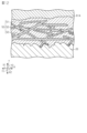
- FIG. 4 is an enlarged cross-sectional view of a portion including the glass film in FIG.
- FIG. 5 is a flow chart illustrating a method for manufacturing an electronic component.
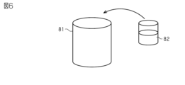
- FIG. 6 is an explanatory diagram for explaining a method for manufacturing an electronic component.
- FIG. 7 is an explanatory diagram for explaining a method for manufacturing an electronic component.
- FIG. 8 is an explanatory diagram for explaining a method for manufacturing an electronic component.
- FIG. 9 is an explanatory diagram for explaining a method for manufacturing an electronic component.
- FIG. 6 is an explanatory diagram for explaining a method for manufacturing an electronic component.
- FIG. 7 is an explanatory diagram for explaining a method for manufacturing an electronic component.
- FIG. 8 is an explanatory diagram for explaining a method for manufacturing an
- FIG. 10 is an explanatory diagram for explaining a method for manufacturing an electronic component.
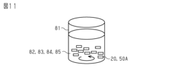
- FIG. 11 is an explanatory diagram for explaining a method for manufacturing an electronic component.
- FIG. 12 is an enlarged cross-sectional view of a portion including a glass film of an electronic component according to a modified example.
- the electronic component 10 is, for example, a surface-mount type negative temperature coefficient thermistor component that is mounted on a circuit board, etc. Note that a negative temperature coefficient thermistor component has a characteristic that its resistance value decreases as the temperature increases.
- the electronic component 10 includes an element body 20.
- the element body 20 is generally rectangular prism-shaped and has a central axis CA.
- an axis extending along the central axis CA is defined as a first axis X.
- One of the axes perpendicular to the first axis X is defined as a second axis Y.
- An axis perpendicular to the first axis X and the second axis Y is defined as a third axis Z.
- One of the directions along the first axis X is defined as a first positive direction X1
- the direction along the first axis X opposite to the first positive direction X1 is defined as a first negative direction X2.
- One of the directions along the second axis Y is defined as a second positive direction Y1, and the direction along the second axis Y opposite to the second positive direction Y1 is defined as a second negative direction Y2.
- One of the directions along the third axis Z is defined as a third positive direction Z1, and the direction along the third axis Z opposite to the third positive direction Z1 is defined as a third negative direction Z2.
- the outer surface 21 of the element body 20 has six flat surfaces 22.
- the "surface” of the element body 20 here refers to a surface that can be observed when the entire element body 20 is observed. In other words, even if there are minute irregularities or steps that cannot be seen unless a part of the element body 20 is magnified and observed with a microscope, the surface is expressed as a flat surface or a curved surface.
- the six flat surfaces 22 extend in different directions.
- the six flat surfaces 22 are broadly divided into a first end surface 22A facing the first positive direction X1, a second end surface 22B facing the first negative direction X2, and four side surfaces 22C.
- the four side surfaces 22C are a surface facing the third positive direction Z1, a surface facing the third negative direction Z2, a surface facing the second positive direction Y1, and a surface facing the second negative direction Y2, respectively.
- the outer surface 21 of the element body 20 has 12 boundary surfaces 23.
- the boundary surfaces 23 include curved surfaces that exist at the boundaries between adjacent flat surfaces 22.
- the boundary surfaces 23 include curved surfaces that are formed, for example, by chamfering the corners that form the adjacent flat surfaces 22.
- the outer surface 21 of the base body 20 also has eight spherical corner surfaces 24.
- the corner surfaces 24 are the boundaries between three adjacent flat surfaces 22.
- the corner surfaces 24 include curved surfaces at the intersections of the three boundary surfaces 23. That is, the corner surfaces 24 include curved surfaces formed, for example, by R-chamfering the corners formed by the three adjacent flat surfaces 22.
- the surface of a glass film 50 described later is regarded as being the same as the outer surface 21 of the element body 20 and is given a reference number.
- the element body 20 has a larger dimension along the first axis X than the dimension along the third axis Z.
- the element body 20 has a larger dimension along the first axis X than the dimension along the second axis Y.
- the material of the element body 20 is a ceramic obtained by sintering a metal oxide containing at least one of Mn, Fe, Ni, Co, Ti, Ba, Al, and Zn.
- the electronic component 10 has two first internal electrodes 41 and two second internal electrodes 42.
- the first internal electrodes 41 and the second internal electrodes 42 are embedded inside the element body 20.
- the material of the first internal electrode 41 is a conductive material.
- the material of the first internal electrode 41 is silver and palladium.
- the material of the second internal electrode 42 is the same as the material of the first internal electrode 41, that is, silver and palladium.
- the first internal electrode 41 has a rectangular plate shape.
- the main surface of the first internal electrode 41 is perpendicular to the second axis Y.
- the second internal electrode 42 has the same rectangular plate shape as the first internal electrode 41.
- the main surface of the second internal electrode 42 is perpendicular to the second axis Y, similar to the first internal electrode 41.
- the dimension of the first internal electrode 41 in the direction along the first axis X is smaller than the dimension of the element body 20 in the direction along the first axis X. Also, as shown in FIG. 1, the dimension of the first internal electrode 41 in the direction along the third axis Z is approximately two-thirds of the dimension of the element body 20 in the direction along the third axis Z. The dimensions of the second internal electrode 42 in each direction are the same as those of the first internal electrode 41.
- the first internal electrodes 41 and the second internal electrodes 42 are positioned alternately in the direction along the second axis Y. That is, from the side surface 22C facing the second positive direction Y1 to the second negative direction Y2, the first internal electrode 41, the second internal electrode 42, the first internal electrode 41, the second internal electrode 42 are arranged in this order. In this embodiment, the distances between each internal electrode in the direction along the second axis Y are equal.
- the two first internal electrodes 41 and the two second internal electrodes 42 are both located at the center of the element body 20 in the direction along the third axis Z.
- the first internal electrode 41 is located closer to the first positive direction X1.
- the second internal electrode 42 is located closer to the first negative direction X2.
- the end of the first internal electrode 41 on the first positive direction X1 side coincides with the end of the element body 20 on the first positive direction X1 side.
- the end of the first internal electrode 41 on the first negative direction X2 side is located inside the element body 20 and does not reach the end of the element body 20 on the first negative direction X2 side.
- the end of the second internal electrode 42 on the first negative direction X2 side coincides with the end of the element body 20 on the first negative direction X2 side.
- the end of the second internal electrode 42 on the first positive direction X1 side is located inside the element body 20 and does not reach the end of the element body 20 on the first positive direction X1 side.
- the electronic component 10 includes a glass film 50.
- the glass film 50 covers the outer surface 21 of the element body 20.
- the glass film 50 covers substantially the entire area of the outer surface 21 of the element body 20.
- the main material of the glass film 50 is insulating glass. Therefore, the glass film 50 contains silicon oxide, specifically silicon dioxide.
- the electronic component 10 has a first external electrode 61 and a second external electrode 62.
- the first external electrode 61 has a first base electrode 61A and a first metal layer 61B.
- the first base electrode 61A is laminated on the glass film 50 in a portion of the outer surface 21 of the element body 20, including the first end face 22A.
- the first base electrode 61A is a five-sided electrode that covers the first end face 22A of the element body 20 and portions of the four side faces 22C on the first positive direction X1 side.
- the material of the first base electrode 61A is copper.
- the first metal layer 61B covers the first base electrode 61A from the outside. Therefore, the first metal layer 61B is laminated on the first base electrode 61A.
- the first metal layer 61B has a two-layer structure of a nickel layer 61C and a tin layer 61D.
- the outer edge of the first metal layer 61B is located outside the outer edge of the first base electrode 61A.
- the outer edge of the first metal layer 61B is located on the surface of the glass film 50. Therefore, a part of the first metal layer 61B is located on the surface of the glass film 50.
- the second external electrode 62 has a second base electrode 62A and a second metal layer 62B.
- the second base electrode 62A is laminated on top of the glass film 50 in a portion of the outer surface 21 of the element body 20, including the second end face 22B.
- the second base electrode 62A is a five-sided electrode that covers the second end face 22B of the element body 20 and portions of the four side faces 22C in the first negative direction X2.
- the material of the second base electrode 62A is the same as the material of the first external electrode 61, that is, copper.
- the second metal layer 62B covers the second base electrode 62A from the outside. Therefore, the second metal layer 62B is laminated on the second base electrode 62A.
- the second metal layer 62B has a two-layer structure of a nickel layer and a tin layer (not shown). Also, as shown in FIG. 3, the outer edge of the second metal layer 62B is located outside the outer edge of the second base electrode 62A. And the outer edge of the second metal layer 62B is located on the surface of the glass film 50. Therefore, a part of the second metal layer 62B is located on the surface of the glass film 50.
- the second external electrode 62 does not reach the first external electrode 61 on the side surface 22C, and is disposed away from the first external electrode 61 in the direction along the first axis X.
- the first external electrode 61 and the second external electrode 62 are not laminated, and the glass film 50 is exposed. Note that in Figures 1 to 3, the first external electrode 61 and the second external electrode 62 are illustrated by two-dot chain lines.
- the first external electrode 61 and the end of the first internal electrode 41 on the first positive direction X1 side are connected via a first penetration portion 71 that penetrates the glass film 50.
- the first penetration portion 71 is formed during the manufacturing process of the electronic component 10 by the silver and palladium that constitute the first internal electrode 41 extending toward the first external electrode 61 side.
- the second external electrode 62 and the end of the second internal electrode 42 on the first negative direction X2 side are connected via a second penetration portion 72 that penetrates the glass film 50.
- the second penetration portion 72 is formed by the silver and palladium that constitute the second internal electrode 42 extending toward the second external electrode 62 during the manufacturing process of the electronic component 10.
- the first internal electrode 41 and the first penetration portion 71 are illustrated as separate members with a boundary, but in reality there is no clear boundary between the two. The same applies to the second penetration portion 72.
- the first penetration portion 71 and the second penetration portion 72 are not illustrated in FIGS. 1 and 2.
- the portion of the glass film 50 that is not covered by either the first base electrode 61A or the second base electrode 62A is a substantially uniform glass layer of silicon dioxide.
- the portion of the glass film 50 that is covered by either the first base electrode 61A or the second base electrode 62A is a mixture of two types of glass layers with different compositions.
- the glass film 50 has a base portion 51 and a specific portion 52. Most of the base portion 51 and the specific portion 52 are located in the glass film 50 between the first base electrode 61A and the outer surface 21 of the element body 20, and between the second base electrode 62A and the outer surface 21 of the element body 20.
- the base portion 51 contains silicon oxide as well as oxides of one or more metal elements selected from alkali metals and alkaline earth metals. In this embodiment, the metal element is barium. In this embodiment, the base portion 51 contains oxides of barium and calcium, which are alkaline earth metals. The base portion 51 also contains zinc oxide. Furthermore, the base portion 51 contains aluminum oxide.
- the specific portion 52 has a flat layer shape when viewed in cross section.
- the specific portion 52 contains oxides of the same metal elements as the base portion 51. That is, in this embodiment, the specific portion 52 contains an oxide of barium, which is an alkaline earth metal. On the other hand, the specific portion 52 does not contain an oxide of calcium. Furthermore, the specific portion 52 contains an oxide of zinc. On the other hand, the specific portion 52 does not contain an oxide of aluminum.
- the content of barium, a metal element, in the specific portion 52 is smaller than the content of barium, a metal element, in the base portion 51.
- the content of silicon in the specific portion 52 is greater than the content of silicon in the base portion 51.
- the content of zinc in the specific portion 52 is greater than the content of zinc in the base portion 51.
- the method for producing electronic component 10 includes a laminate preparation step S11, an R-chamfering process step S12, a solvent introduction step S13, a catalyst introduction step S14, an element introduction step S15, a polymer introduction step S16, and a metal alkoxide introduction step S17.
- the method for producing electronic component 10 further includes a film formation step S18, a drying step S19, a baking step S20, a conductor application step S21, a curing step S22, and a plating step S23.
- a laminate which is the element body 20 that does not have boundary surfaces 23 and corner surfaces 24. That is, the laminate is in a state before R-chamfering and has a rectangular parallelepiped shape with six flat surfaces 22.
- a plurality of ceramic sheets that will become the element body 20 are prepared. The sheets are thin plate-like. A conductive paste that will become the first internal electrode 41 is laminated on the sheets. A ceramic sheet that will become the element body 20 is laminated on the laminated paste. A conductive paste that will become the second internal electrode 42 is laminated on the sheet. In this way, the ceramic sheet and the conductive paste are laminated. Then, by cutting to a predetermined size, an unfired laminate is formed. After that, the unfired laminate is fired at a high temperature to prepare the laminate.
- the R-chamfering process S12 is performed.
- the boundary surface 23 and the corner surface 24 are formed on the laminate prepared in the laminate preparation process S11.
- the corners of the laminate are R-chamfered by barrel polishing, thereby forming the boundary surface 23 having a curved surface and the corner surface 24 having a curved surface. In this way, the base body 20 is formed.
- a catalyst introduction step S14 is performed as shown in Fig. 5.
- Fig. 7 in the catalyst introduction step S14, first, stirring of the solvent 82 in the reaction vessel 81 is started. Then, ammonia water is introduced into the reaction vessel 81 as an aqueous solution 83 containing a catalyst.
- the catalyst in this embodiment is a hydroxide ion, which functions as a catalyst for promoting hydrolysis of a metal alkoxide 85 described later.
- the element introduction step S15 is performed. As shown in FIG. 8, in the element introduction step S15, a plurality of element bodies 20 that have been previously formed in the R chamfering step S12 as described above are introduced into a reaction vessel 81.
- a polymer introduction step S16 is performed.
- polyvinylpyrrolidone is introduced into the reaction vessel 81 as the polymer 84.
- the polymer 84 introduced into the reaction vessel 81 is adsorbed onto the outer surface 21 of the element body 20.
- a metal alkoxide introduction step S17 is performed.
- liquid tetraethyl orthosilicate is introduced into the reaction vessel 81 as the metal alkoxide 85.
- tetraethyl orthosilicate is also called tetraethoxysilane.
- the amount of metal alkoxide 85 introduced in the metal alkoxide introduction step S17 is calculated based on the area of the outer surface 21 of the element body 20 introduced in the element introduction step S15.
- the amount of metal alkoxide 85 per element body 20 required to form a pre-diffusion glass film 50A covering the outer surface 21 of the element body 20 is multiplied by the number of element bodies 20 to calculate the amount.
- the pre-diffusion glass film 50A is a film in a state before diffusion of the metal elements contained in the glass of the conductor paste occurs, as described later. In other words, the pre-diffusion glass film 50A does not contain any metal elements derived from the conductor paste.
- the film formation process S18 is performed.
- the stirring of the solvent 82 started in the above-mentioned solvent introduction process S13 is continued for a predetermined time after the metal alkoxide 85 is introduced into the reaction vessel 81 in the metal alkoxide introduction process S17.
- a pre-diffusion glass film 50A is formed by a liquid phase reaction in the reaction vessel 81.
- a drying step S19 is performed.
- the element body 20 is removed from the reaction vessel 81 and dried.
- the sol-like pre-diffusion glass film 50A is dried and becomes a gel-like pre-diffusion glass film 50A.
- the firing step S20 is performed.
- the base body 20 covered with the gel-like pre-diffusion glass film 50A is heated. This causes the water and polymer 84 to evaporate from the gel-like pre-diffusion glass film 50A. As a result, a pre-diffusion glass film 50A made of silicon dioxide is formed.
- the conductor application step S21 is performed.
- a conductor paste is applied to two portions of the surface of the pre-diffusion glass film 50A, namely, a portion including a portion covering the first end face 22A of the element 20, and a portion including a portion covering the second end face 22B of the element 20.
- the conductor paste is applied to cover the glass film 50 on the entire first end face 22A and a portion on the four side faces 22C.
- the conductor paste is also applied to cover the pre-diffusion glass film 50A on the entire second end face 22B and a portion on the four side faces 22C.
- the conductor paste contains copper powder, glass, and an organic medium.
- the copper powder of the conductor paste becomes the first base electrode 61A and the second base electrode 62A by the subsequent hardening step S22.
- the glass of the conductor paste contains an additive containing one or more metal elements selected from alkali metals and alkaline earth metals. More specifically, the metal element is barium. Additionally, the conductive paste contains calcium, aluminum, and zinc as additives.
- the hardening step S22 is performed. Specifically, in the hardening step S22, the pre-diffusion glass film 50A and the base body 20 to which the conductive paste has been applied are heated. This causes the organic medium in the conductive paste to evaporate. The copper powder in the conductive paste then combines to form the first base electrode 61A and the second base electrode 62A. In other words, the material of the first base electrode 61A and the second base electrode 62A is copper. Note that the first base electrode 61A and the second base electrode 62A may contain impurities.
- the glass in the conductor paste melts and becomes integrated with a portion of the pre-diffusion glass film 50A.
- the pre-diffusion glass film 50A is composed of almost only silicon oxide. Therefore, the pre-diffusion glass film 50A has a high melting point. Therefore, a portion of the pre-diffusion glass film 50A does not become integrated with the glass of the conductor paste and remains.
- the metal elements contained in the glass additive in the conductor paste diffuse into the pre-diffusion glass film 50A made of silicon dioxide. As a result, the metal elements penetrate into the pre-diffusion glass film 50A covering the outer surface 21 of the element body 20.
- the mixture of the glass derived from the conductor paste and the pre-diffusion glass film 50A becomes the base portion 51.
- the pre-diffusion glass film 50A that remains without being integrated with the glass of the conductor paste becomes the specific portion 52.
- the metal elements are also diffused into the pre-diffusion glass film 50A that remains without being integrated with the glass of the conductor paste. Therefore, the specific portion 52 contains a metal element, although in smaller amounts, compared to the base portion 51.
- the diffusion of metal elements as described above is unlikely to occur in the areas that are not covered with the conductive paste. Therefore, in the pre-diffusion glass film 50A, the areas that are not covered with the conductive paste become a generally uniform layer of glass with no distinction between the base portion 51 and the specific portion 52.
- the Kirkendall effect which arises from the difference in diffusion speed between the first internal electrode 41 and the first base electrode 61A, attracts the silver and palladium contained in the first internal electrode 41 to the first base electrode 61A, which is copper.
- the first penetration portion 71 extends from the first internal electrode 41 toward the first base electrode 61A through the glass film 50, connecting the first internal electrode 41 to the first base electrode 61A.
- the second penetration portion 72 that connects the second internal electrode 42 to the second base electrode 62A.
- the plating step S23 is performed.
- electroplating is performed on the first base electrode 61A and the second base electrode 62A.
- a first metal layer 61B is formed on the surface of the first base electrode 61A.
- a second metal layer 62B is formed on the surface of the second base electrode 62A.
- the first metal layer 61B is electroplated with two types of metal, nickel and tin, to form a two-layer structure of a nickel layer 61C and a tin layer 61D.
- the second metal layer 62B is electroplated with two types of metal, nickel and tin, in that order to form a two-layer structure of a nickel layer and a tin layer. In this manner, the electronic component 10 is formed.
- the electronic component 10 of the above embodiment is surface-treated with a water-soluble flux when solder-mounted on a substrate, etc. At this time, the water-soluble flux may penetrate into the glass film 50 from the interface between the first external electrode 61 and the glass film 50, and further into the element body 20.
- the glass film 50 has a base portion 51 and a specific portion 52.
- the specific portion 52 contains silicon oxide and an oxide of a metal element.
- the content ratio of the metal element in the specific portion 52 is smaller than the content ratio of the metal element in the base portion 51. Therefore, an interface between the base portion 51 and the specific portion 52 can be present in the glass film 50. If an interface is present in the glass film 50 in this way, even if the water-soluble flux penetrates into the glass film 50, the water-soluble flux will extend on the interface. Therefore, the water-soluble flux that has penetrated is unlikely to penetrate deeper than the interface between the base portion 51 and the specific portion 52. Therefore, it is possible to more effectively prevent erosion of the element body 20 from the outside.
- the silicon content of the specific portion 52 is greater than the silicon content of the base portion 51. In this way, the composition of the specific portion 52 is different from the composition of the base portion 51. Therefore, the interface between the base portion 51 and the specific portion 52 becomes clearer.
- the metal element is barium, which is an alkaline earth metal.
- barium is relatively easy to obtain. Therefore, there is no need to prepare an element that is difficult to obtain.
- the specifying portion 52 contains zinc oxide. Therefore, the containing of zinc tends to result in a stable composition containing barium, which is an alkaline earth metal.
- the zinc content of the specific portion 52 is greater than the zinc content of the base portion 51. Therefore, the composition of the specific portion 52 is different from the composition of the base portion 51. Therefore, the interface between the base portion 51 and the specific portion 52 becomes clearer.
- the first external electrode 61 has the first metal layer 61B. Therefore, there is a high possibility that the electronic component 10 will be used by being mounted on a substrate or the like by soldering. In other words, there is a high possibility that the electronic component 10 will be exposed to water-soluble flux. Therefore, the effect of preventing the intrusion of water-soluble flux is very significant.
- the first metal layer 61B extends over a wider area than the first base electrode 61A. Therefore, a part of the first metal layer 61B is also located on the surface of the glass film 50. Therefore, when the outer edge of the first metal layer 61B is located outside the outer edge of the first base electrode 61A, it is possible to prevent a gap from being generated between the first external electrode 61 and the glass film 50. Preventing such a gap from being generated makes it easier to prevent the intrusion of water-soluble flux from between the first external electrode 61 and the glass film 50.
- the electronic component 10 is not limited to a negative characteristic thermistor component.
- it may be a thermistor component other than a negative characteristic, or it may be a multilayer capacitor component or an inductor component.
- the material of the element body 20 is not limited to that in the above embodiment.
- the material of the element body 20 may be a composite body of resin and metal powder.
- the shape of the element body 20 is not limited to the example of the above embodiment.
- the element body 20 may be a polygonal columnar shape other than a quadrangular columnar shape having a central axis CA.
- the element body 20 may also be a core of a wire-wound inductor component.
- the core may have a so-called drum core shape.
- the core may have a columnar winding core portion and flange portions provided at each end of the winding core portion.
- the outer surface 21 of the element body 20 may not have boundary surfaces 23 and corner surfaces 24.
- boundary surfaces 23 and corner surfaces 24 may not exist.
- the shape of the first internal electrode 41 and the second internal electrode 42 does not matter as long as it can ensure electrical conduction with the corresponding first external electrode 61 and second external electrode 62.
- the number of first internal electrodes 41 and second internal electrodes 42 does not matter, and the number of internal electrodes may be one or three or more.
- the configuration of the first external electrode 61 is not limited to the example of the above embodiment.
- the first external electrode 61 may be composed of only the first base electrode 61A, and the first metal layer 61B may not have a two-layer structure. The same applies to the second external electrode 62.
- the combination of materials between the first internal electrode 41 and the first base electrode 61A is not limited to a combination of copper on one side and silver and palladium on the other side.
- it may be a combination of palladium and silver, copper and nickel, copper and silver, copper and palladium, silver and gold, nickel and cobalt, or nickel and gold.
- it may be a combination of copper on one side and copper and nickel on the other.
- it may be a combination of nickel on one side and copper and nickel on the other.
- it may be a combination of gold on one side and silver and palladium on the other.
- the Kirkendall effect may not be obtained.
- the first internal electrode 41 may be processed to be exposed before the external electrode formation process.
- the first end surface 22A side of the element body 20 may be polished to physically remove a part of the glass film 50.
- the base electrode formation process may then be performed to connect the first internal electrode 41 and the first base electrode 61A.
- the glass film 50 may be formed including the surface of the first base electrode 61A, and the glass film 50 covering the surface of the first base electrode 61A may be removed. This also applies to the combination of materials for the second internal electrode 42 and the second base electrode 62A.
- the location of the first external electrode 61 is not limited to the example of the above embodiment.
- the first external electrode 61 may be disposed only on the first end surface 22A and one side surface 22C.
- the glass film 50 does not have to cover the entire area of the outer surface 21 of the element body 20.
- the area covered by the glass film 50 may be changed as appropriate depending on the shape of the element body 20, the positions of the first external electrode 61 and the second external electrode 62, etc.
- the metal element contained in the glass film 50 may be an alkali metal.
- the metal element contained in the glass film 50 may be any of the alkali metals lithium, sodium, and potassium. Among the alkali metals, lithium, sodium, and potassium are relatively easy to obtain. Therefore, there is no need to prepare an element that is difficult to obtain.
- the metal element contained in the glass film 50 may be calcium, which is an alkaline earth metal.
- the metal contained in the glass film 50 may also be another alkaline earth metal.
- the specific portion 52 may contain aluminum oxide.
- the specific portion 52 may contain zinc oxide.
- the base portion 51 and the specific portion 52 may contain additives of other elements. Depending on the content ratio of the other elements, the silicon content ratio of the specific portion 52 may be equal to or lower than the silicon content ratio of the base portion 51.
- the base portion 51 may not contain aluminum oxide.
- the base portion 51 may not contain zinc oxide.
- the zinc content of the specific portion 52 may be equal to or less than the zinc content of the base portion 51.
- the material of the glass film 50 is not limited to the example of the above embodiment.
- the glass is not limited to silicon dioxide, and may be a multi-component oxide containing Si, such as B-Si, Si-Zn, Zr-Si, or Al-Si oxides.
- the glass may also be a multi-component oxide containing an alkali metal and Si, such as Al-Si, Na-Si, K-Si, or Li-Si oxides.
- the glass may also be a multi-component oxide containing an alkaline earth metal and Si, such as Mg-Si, Ca-Si, Ba-Si, or Sr-Si.
- the glass may not contain Si, and may be a mixture of these. If the material of the glass film 50 contains boron, the specific portion 52 may contain boron oxide. In this case, the base portion 51 may also contain boron oxide.
- the material of the glass film 50 may also contain a surface treatment agent or an antistatic agent, such as a pigment, a silicone-based flame retardant, a silane coupling agent, or a titanate coupling agent.
- a surface treatment agent or an antistatic agent such as a pigment, a silicone-based flame retardant, a silane coupling agent, or a titanate coupling agent.
- the glass film 50 may contain, in addition to glass, additives such as organic acid salts, oxides, inorganic salts, organic salts, and other fine particles and nanoparticles of metal oxides.
- additives such as organic acid salts, oxides, inorganic salts, organic salts, and other fine particles and nanoparticles of metal oxides.
- organic acid salts include salts of oxoacids such as soda ash, sodium carbonate, sodium hydrogencarbonate, sodium percarbonate, sodium sulfite, sodium hydrogensulfite, sodium sulfate, sodium thiosulfate, sodium nitrate, and sodium sulfite; and halogen compounds such as sodium fluoride, sodium chloride, sodium bromide, and sodium iodide.
- An example of the oxide is sodium peroxide
- an example of the hydroxide is sodium hydroxide.
- examples of inorganic salts include sodium hydride, sodium sulfide, sodium hydrogen sulfide, sodium silicate, trisodium phosphate, sodium borate, sodium borohydride, sodium cyanide, sodium cyanate, and sodium tetrachloroaurate.
- inorganic salts include calcium peroxide, calcium hydroxide, calcium fluoride, calcium chloride, calcium bromide, calcium iodide, calcium hydride, calcium carbide, and calcium phosphide.
- Additives may also be oxoacid salts such as calcium carbonate, calcium bicarbonate, calcium nitrate, calcium sulfate, calcium sulfite, calcium silicate, calcium phosphate, calcium pyrophosphate, calcium hypochlorite, calcium chlorate, calcium perchlorate, calcium bromate, calcium iodate, calcium arsenite, calcium chromate, calcium tungstate, calcium molybdate, calcium magnesium carbonate, and hydroxyapatite.
- Additives may also include calcium acetate, calcium gluconate, calcium citrate, calcium malate, calcium lactate, calcium benzoate, calcium stearate, and calcium aspartate.
- the additive may be lithium carbonate, lithium chloride, lithium titanate, lithium nitride, lithium peroxide, lithium citrate, lithium fluoride, lithium hexafluorophosphate, lithium acetate, lithium iodide, lithium hypochlorite, lithium tetraborate, lithium bromide, lithium nitrate, lithium hydroxide, lithium aluminum hydride, lithium triethylborohydride, lithium hydride, lithium amide, lithium imide, lithium diisopropylamide, lithium tetramethylpiperidide, lithium sulfide, lithium sulfate, lithium thiophenolate, or lithium phenoxide.
- the additive may be boron triiodide, sodium cyanoborohydride, sodium borohydride, tetrafluoroboric acid, triethylborane, borax, or boric acid.
- additives include potassium arsenide, potassium bromide, potassium carbide, potassium chloride, potassium fluoride, potassium hydride, potassium iodide, potassium triiodide, potassium azide, potassium nitride, potassium superoxide, potassium ozonate, potassium peroxide, potassium phosphide, potassium sulfide, potassium selenide, potassium telluride, potassium tetrafluoroaluminate, potassium tetrafluoroborate, potassium tetrahydroborate, potassium methanide, potassium cyanide, potassium formate, potassium hydrogen fluoride, and tetramercury iodide.
- the additive may be barium sulfite, barium chloride, barium chlorate, barium perchlorate, barium peroxide, barium chromate, barium acetate, barium cyanide, barium bromide, barium oxalate, barium nitrate, barium hydroxide, barium hydride, barium carbonate, barium iodide, barium sulfide, or barium sulfate.
- the additive may be sodium acetate or sodium citrate.
- the additive may also be fine particles or nanoparticles of metal oxides, such as sodium oxide, calcium oxide, lithium oxide, boron oxide, potassium oxide, barium oxide, silicon oxide, titanium oxide, zirconium oxide, aluminum oxide, zinc oxide, and magnesium oxide.
- metal oxides such as sodium oxide, calcium oxide, lithium oxide, boron oxide, potassium oxide, barium oxide, silicon oxide, titanium oxide, zirconium oxide, aluminum oxide, zinc oxide, and magnesium oxide.
- the specific portion 52 is not limited to one layer.
- the number of the specific portions 52 may be multiple.
- the shape of the specific portions 52 does not have to be layered.
- the glass film 50 has multiple specific portions 52.
- the major axis of the specific portion 52 When viewed in cross section on a plane perpendicular to the outer surface 21 of the base body 20, the major axis of the specific portion 52 is three times or more the minor axis.
- the major axis is the maximum length of the line segment that passes through the geometric center of one specific portion 52 and can be drawn from outer edge to outer edge when viewed in cross section.
- the minor axis is the length of the line segment that passes through the geometric center of the same specific portion 52, is perpendicular to the major axis, and can be drawn from outer edge to outer edge when viewed in cross section.
- the major axis of one specific portion 52 is three times or more the minor axis, that is, the specific portion 52 is plate-shaped or needle-shaped when viewed in cross section. This allows the path from the outside of the glass film 50 through the base portion 51 to the element body 20 to be complex. It also increases the likelihood that more interfaces will be aligned in the direction perpendicular to the outer surface 21 of the element body 20.
- the metal alkoxide 85 may be, for example, sodium methoxide, sodium ethoxide, calcium diethoxide, lithium isopropoxide, lithium ethoxide, lithium tert-butoxide, lithium methoxide, boron alkoxide, potassium t-butoxide, tetraethyl orthosilicate, allyltrimethoxysilane, isobutyl(trimethoxy)silane, tetrapropyl orthosilicate, tetramethyl orthosilicate, [3-(diethylamino)propyl]trimethylsilane, triethoxysilane, triethoxy(octyl)silane, triethoxyvinylsilane, triethoxyphenylsilane, trimethoxyphenylsilane, trimethoxymethylsilane, butyltrichlorosilane, n-propyltriethoxys
- a metal complex or acetate which is a precursor of the metal alkoxide 85, may be used instead of the metal alkoxide 85.
- a metal complex or acetate which is a precursor of the metal alkoxide, may be introduced.
- Examples of the metal complex include acetylacetonates such as lithium acetylacetonate, titanium (IV) oxyacetylacetonate, titanium diisopropoxide bis(acetylacetonate), zirconium (IV) trifluoroacetylacetonate, zirconium (IV) acetylacetonate, aluminum acetylacetonate, aluminum (III) acetylacetonate, calcium (II) acetylacetonate, and zinc (II) acetylacetonate.
- Examples of acetate include zirconium acetate, zirconium (IV) hydroxide acetate, and basic aluminum acetate.
- the manufacturing method of the electronic component 10 is not limited to the above embodiment.
- the solvent introduction step S13 may be performed after the catalyst introduction step S14 or the element introduction step S15.
- the solvent 82 is not limited to 2-propanol. The solvent 82 may be changed as appropriate as long as it can sufficiently disperse the metal alkoxide 85.
- ⁇ 3> The electronic component according to ⁇ 1> or ⁇ 2>, wherein the metal element is any one of alkali metals, lithium, sodium, and potassium.
- ⁇ 4> The electronic component according to ⁇ 1> or ⁇ 2>, wherein the metal element is either calcium or barium, which is an alkaline earth metal.
- ⁇ 5> The electronic component according to any one of ⁇ 1> to ⁇ 4>, wherein the specific portion contains an oxide of any one of elements of zinc, boron, and aluminum.
- the base portion includes zinc oxide;
- the specific portion contains zinc oxide,
- the electronic component according to ⁇ 5>, wherein the specific portion has a higher zinc content than the base portion.
- the glass film has a plurality of the specific portions, When viewed in cross section, the longest length of a line segment that passes through the geometric center of the specific portion and can be drawn from one outer edge to the other is defined as the major axis; When viewed in cross section, the length of a line segment that passes through the geometric center of the specific portion, is perpendicular to the major axis, and can be drawn from one outer edge to the other outer edge is defined as the minor axis.
- the electronic component according to any one of ⁇ 1> to ⁇ 6>, wherein the major axis is three or more times the minor axis.
- the external electrode further includes a metal layer, The electronic component according to any one of ⁇ 1> to ⁇ 7>, wherein the metal layer is provided on a surface of the base electrode.
- Reference Signs List 10 Electronic component 20: Body 21: Outer surface 50: Glass film 51: Base portion 52: Specific portion 61: First external electrode 61A: First base electrode 61B: First metal layer
Landscapes
- Engineering & Computer Science (AREA)
- Power Engineering (AREA)
- Microelectronics & Electronic Packaging (AREA)
- Physics & Mathematics (AREA)
- Electromagnetism (AREA)
- Manufacturing & Machinery (AREA)
- Fixed Capacitors And Capacitor Manufacturing Machines (AREA)
Abstract
Description
以下、電子部品の一実施形態を、図面を参照して説明する。なお、図面は、理解を容易にするために構成要素を拡大して示している場合がある。構成要素の寸法比率は実際のものと、又は別の図面中のものと異なる場合がある。
図1に示すように、電子部品10は、例えば、回路基板等に実装される表面実装型の負特性サーミスタ部品である。なお、負特性サーミスタ部品は、温度が上がると抵抗値が下がるという特性を有するものである。
図2に示すように、素体20は、第1軸Xに沿う方向の寸法が、第3軸Zに沿う方向の寸法よりも大きい。また、図1に示すように、素体20は、第1軸Xに沿う方向の寸法が、第2軸Yに沿う方向の寸法よりも大きい。また、素体20の材質は、Mn、Fe、Ni、Co、Ti、Ba、Al、及びZnの少なくとも1つを成分とする金属酸化物を焼成したセラミックスである。
ガラス膜50のうち第1下地電極61A及び第2下地電極62Aの双方に覆われていない箇所は、概ね均一な二酸化ケイ素のガラス層となっている。一方、ガラス膜50のうち、第1下地電極61A及び第2下地電極62Aのいずれかに覆われている箇所は、組成の異なる2種類のガラス層の混合物になっている。
次に、電子部品10の製造方法について説明する。
図5に示すように、電子部品10の製造方法は、積層体準備工程S11と、R面取り加工工程S12と、溶媒投入工程S13と、触媒投入工程S14と、素体投入工程S15と、ポリマー投入工程S16と、金属アルコキシド投入工程S17と、を備えている。また、電子部品10の製造方法は、成膜工程S18と、乾燥工程S19と、焼成工程S20と、導電体塗布工程S21と、硬化工程S22と、めっき工程S23と、をさらに備えている。
次に、図5に示すように、触媒投入工程S14を行う。図7に示すように、触媒投入工程S14では、先ず、反応容器81内の溶媒82の撹拌を開始する。そして、反応容器81内に、触媒を含む水溶液83として、アンモニア水を投入する。この実施形態における触媒は、水酸化物イオンであり、後述する金属アルコキシド85の加水分解を促進する触媒として機能する。
上記実施形態の電子部品10は、基板等にはんだ実装される際に、水溶性フラックスを用いて表面処理される。このとき、水溶性フラックスは、第1外部電極61とガラス膜50との界面からガラス膜50の内部に浸入し、さらに素体20へと浸入することがある。
(1)上記実施形態によれば、ガラス膜50は、ベース部51と、特定部52と、を有している。そして、特定部52は、ケイ素酸化物及び金属元素の酸化物を含んでいる。そして、特定部52の金属元素の含有割合は、ベース部51の金属元素の含有割合よりも小さい。そのため、ガラス膜50の中に、ベース部51と特定部52との界面を存在させることができる。このようにガラス膜50中にも界面が存在すると、仮にガラス膜50中に水溶性フラックスが浸入しても、水溶性フラックスが界面上を延びていく。そのため、浸入した水溶性フラックスがベース部51と特定部52との界面より奥には浸透しにくい。よって、外部から素体20への浸食をより防止できる。このように、上記実施形態によれば、シリカ粉末の添加を必ずしも要さずに、耐フラックス性を向上させることができる。
(5)上記実施形態によれば、特定部52の亜鉛の含有割合は、ベース部51の亜鉛の含有割合よりも大きい。そのため、特定部52の組成が、ベース部51の組成と異なっている。よって、ベース部51と特定部52との界面がより明確になる。
上記実施形態は以下のように変更して実施することができる。上記実施形態及び以下の変更例は、技術的に矛盾しない範囲で組み合わせて実施することができる。
・素体20の形状は、上記実施形態の例に限られない。例えば、素体20は、中心軸線CAを有する四角形柱状以外の多角形柱状であってもよい。また、素体20は、巻線型のインダクタ部品のコアであってもよい。例えば、コアは、いわゆるドラムコア形状であってもよい。具体的には、コアは、柱状の巻芯部と、巻芯部の各端部に設けられた鍔部とを有していてもよい。
・ガラス膜50は、素体20の外表面21のすべての領域を覆っていなくてもよい。素体20の形状、第1外部電極61及び第2外部電極62の位置等に併せて、ガラス膜50が覆う範囲は、適宜変更されればよい。
有機酸塩としては、例えば、ソーダ灰、炭酸ナトリウム、炭酸水素ナトリウム、過炭酸ナトリウム、亜硫酸ナトリウム、亜硫酸水素ナトリウム、硫酸ナトリウム、チオ硫酸ナトリウム、硝酸ナトリウム、亜硫酸ナトリウムといったオキソ酸の塩やフッ化ナトリウム、塩化ナトリウム、臭化ナトリウム、ヨウ化ナトリウムといったハロゲン化合物が挙げられる。
無機塩としては、例えば、水素化ナトリウム、硫化ナトリウム、硫化水素ナトリウム、珪酸ナトリウム、リン酸三ナトリウム、ほう酸ナトリウム、水素化ホウ素ナトリウム、シアン化ナトリウム、シアン酸ナトリウム、テトラクロロ金酸ナトリウムが挙げられる。
<1>
素体と、
前記素体の外表面を覆うガラス膜と、
前記ガラス膜の外表面に積層され、少なくとも下地電極を有する外部電極と、を備え、
前記ガラス膜は、ケイ素酸化物に加えてアルカリ金属及びアルカリ土類金属のうちの1種類以上の金属元素の酸化物を含むベース部と、ケイ素酸化物に加えて前記ベース部と同じ前記金属元素の酸化物を含む特定部を有し、
前記特定部における前記金属元素の含有割合は、前記ベース部における前記金属元素の含有割合よりも小さい
電子部品。
前記特定部のケイ素の含有割合は、前記ベース部のケイ素の含有割合よりも大きい
<1>に記載の電子部品。
前記金属元素は、アルカリ金属のうちのリチウム、ナトリウム、及びカリウムのいずれかである
<1>又は<2>に記載の電子部品。
前記金属元素は、アルカリ土類金属のうちのカルシウム、及びバリウムのいずれかである
<1>又は<2>に記載の電子部品。
前記特定部は、亜鉛、ホウ素、及びアルミニウムのいずれかの元素の酸化物を含んでいる
<1>~<4>のいずれか1つに記載の電子部品。
前記ベース部は、亜鉛酸化物を含んでおり、
前記特定部は、亜鉛酸化物を含んでおり、
前記特定部の亜鉛の含有割合は、前記ベース部の亜鉛の含有割合よりも大きい
<5>に記載の電子部品。
前記ガラス膜は、複数の前記特定部を有しており、
断面視したときに、前記特定部の幾何中心を通り、且つ外縁から外縁へと引ける線分の長さのうちの最大の長さを長径とし、
前記断面視したときに、前記特定部の幾何中心を通り、前記長径に対して直交し、外縁から外縁へと引ける線分の長さを短径としたとき、
前記長径は、前記短径の3倍以上である
<1>~<6>のいずれか1つに記載の電子部品。
前記外部電極は、金属層をさらに有しており、
前記金属層は、前記下地電極の表面上に設けられている
<1>~<7>のいずれか1つに記載の電子部品。
前記金属層の一部は、前記ガラス膜の表面上に位置している
<8>に記載の電子部品。
20…素体
21…外表面
50…ガラス膜
51…ベース部
52…特定部
61…第1外部電極
61A…第1下地電極
61B…第1金属層
Claims (9)
- 素体と、
前記素体の外表面を覆うガラス膜と、
前記ガラス膜の外表面に積層され、少なくとも下地電極を有する外部電極と、を備え、
前記ガラス膜は、ケイ素酸化物に加えてアルカリ金属及びアルカリ土類金属のうちの1種類以上の金属元素の酸化物を含むベース部と、ケイ素酸化物に加えて前記ベース部と同じ前記金属元素の酸化物を含む特定部を有し、
前記特定部における前記金属元素の含有割合は、前記ベース部における前記金属元素の含有割合よりも小さい
電子部品。 - 前記特定部のケイ素の含有割合は、前記ベース部のケイ素の含有割合よりも大きい
請求項1に記載の電子部品。 - 前記金属元素は、アルカリ金属のうちのリチウム、ナトリウム、及びカリウムのいずれかである
請求項1又は2に記載の電子部品。 - 前記金属元素は、アルカリ土類金属のうちのカルシウム、及びバリウムのいずれかである
請求項1又は2に記載の電子部品。 - 前記特定部は、亜鉛、ホウ素、及びアルミニウムのいずれかの元素の酸化物を含んでいる
請求項1~4のいずれか一項に記載の電子部品。 - 前記ベース部は、亜鉛酸化物を含んでおり、
前記特定部は、亜鉛酸化物を含んでおり、
前記特定部の亜鉛の含有割合は、前記ベース部の亜鉛の含有割合よりも大きい
請求項5に記載の電子部品。 - 前記ガラス膜は、複数の前記特定部を有しており、
断面視したときに、前記特定部の幾何中心を通り、且つ外縁から外縁へと引ける線分の長さのうちの最大の長さを長径とし、
前記断面視したときに、前記特定部の幾何中心を通り、前記長径に対して直交し、外縁から外縁へと引ける線分の長さを短径としたとき、
前記長径は、前記短径の3倍以上である
請求項1~6のいずれか一項に記載の電子部品。 - 前記外部電極は、金属層をさらに有しており、
前記金属層は、前記下地電極の表面上に設けられている
請求項1~7のいずれか一項に記載の電子部品。 - 前記金属層の一部は、前記ガラス膜の表面上に位置している
請求項8に記載の電子部品。
Priority Applications (3)
| Application Number | Priority Date | Filing Date | Title |
|---|---|---|---|
| JP2024552827A JP7687537B2 (ja) | 2022-10-28 | 2023-07-03 | 電子部品 |
| CN202380036449.0A CN119096311A (zh) | 2022-10-28 | 2023-07-03 | 电子部件 |
| US18/667,780 US20240304363A1 (en) | 2022-10-28 | 2024-05-17 | Electronic component |
Applications Claiming Priority (2)
| Application Number | Priority Date | Filing Date | Title |
|---|---|---|---|
| JP2022173538 | 2022-10-28 | ||
| JP2022-173538 | 2022-10-28 |
Related Child Applications (1)
| Application Number | Title | Priority Date | Filing Date |
|---|---|---|---|
| US18/667,780 Continuation US20240304363A1 (en) | 2022-10-28 | 2024-05-17 | Electronic component |
Publications (1)
| Publication Number | Publication Date |
|---|---|
| WO2024089941A1 true WO2024089941A1 (ja) | 2024-05-02 |
Family
ID=90830520
Family Applications (1)
| Application Number | Title | Priority Date | Filing Date |
|---|---|---|---|
| PCT/JP2023/024562 Ceased WO2024089941A1 (ja) | 2022-10-28 | 2023-07-03 | 電子部品 |
Country Status (4)
| Country | Link |
|---|---|
| US (1) | US20240304363A1 (ja) |
| JP (1) | JP7687537B2 (ja) |
| CN (1) | CN119096311A (ja) |
| WO (1) | WO2024089941A1 (ja) |
Cited By (1)
| Publication number | Priority date | Publication date | Assignee | Title |
|---|---|---|---|---|
| WO2025249191A1 (ja) * | 2024-05-31 | 2025-12-04 | 株式会社村田製作所 | 電子部品 |
Citations (2)
| Publication number | Priority date | Publication date | Assignee | Title |
|---|---|---|---|---|
| JPH05251210A (ja) * | 1991-12-20 | 1993-09-28 | Mitsubishi Materials Corp | 導電性チップ型セラミック素子及びその製造方法 |
| JP2021027163A (ja) * | 2019-08-05 | 2021-02-22 | 三菱マテリアル株式会社 | 保護膜付きサーミスタおよびその製造方法 |
Family Cites Families (3)
| Publication number | Priority date | Publication date | Assignee | Title |
|---|---|---|---|---|
| JPS598323A (ja) * | 1982-07-05 | 1984-01-17 | 松下電器産業株式会社 | 積層セラミツクコンデンサの製造方法 |
| JP4254359B2 (ja) * | 2003-06-11 | 2009-04-15 | 株式会社村田製作所 | チップ型セラミック電子部品の製造方法 |
| JP2014053551A (ja) * | 2012-09-10 | 2014-03-20 | Tdk Corp | セラミック電子部品 |
-
2023
- 2023-07-03 CN CN202380036449.0A patent/CN119096311A/zh active Pending
- 2023-07-03 WO PCT/JP2023/024562 patent/WO2024089941A1/ja not_active Ceased
- 2023-07-03 JP JP2024552827A patent/JP7687537B2/ja active Active
-
2024
- 2024-05-17 US US18/667,780 patent/US20240304363A1/en active Pending
Patent Citations (2)
| Publication number | Priority date | Publication date | Assignee | Title |
|---|---|---|---|---|
| JPH05251210A (ja) * | 1991-12-20 | 1993-09-28 | Mitsubishi Materials Corp | 導電性チップ型セラミック素子及びその製造方法 |
| JP2021027163A (ja) * | 2019-08-05 | 2021-02-22 | 三菱マテリアル株式会社 | 保護膜付きサーミスタおよびその製造方法 |
Cited By (1)
| Publication number | Priority date | Publication date | Assignee | Title |
|---|---|---|---|---|
| WO2025249191A1 (ja) * | 2024-05-31 | 2025-12-04 | 株式会社村田製作所 | 電子部品 |
Also Published As
| Publication number | Publication date |
|---|---|
| CN119096311A (zh) | 2024-12-06 |
| JPWO2024089941A1 (ja) | 2024-05-02 |
| US20240304363A1 (en) | 2024-09-12 |
| JP7687537B2 (ja) | 2025-06-03 |
Similar Documents
| Publication | Publication Date | Title |
|---|---|---|
| US12476049B2 (en) | Electronic component and method for manufacturing the same | |
| US5750264A (en) | Electronic component and method for fabricating the same | |
| US20240021347A1 (en) | Electronic component | |
| JP3555563B2 (ja) | 積層チップバリスタの製造方法および積層チップバリスタ | |
| JP7622842B2 (ja) | 電子部品 | |
| JP7687537B2 (ja) | 電子部品 | |
| US20240021346A1 (en) | Electronic component | |
| US12308174B2 (en) | Electronic component | |
| US20250266189A1 (en) | Protective glass film | |
| US20250232899A1 (en) | Electronic component and film forming method | |
| CN113840812A (zh) | 表面改性玻璃、电子部件和硅酸盐被膜的形成方法 | |
| US20240221981A1 (en) | Electronic component and film forming method | |
| WO2024262064A1 (ja) | 電子部品 | |
| WO2025249192A1 (ja) | 電子部品 | |
| JP3013719B2 (ja) | 電子部品の製造方法 | |
| WO2025249191A1 (ja) | 電子部品 | |
| WO2025169709A1 (ja) | 電子部品 | |
| EP2620418A1 (en) | Glass-ceramic composite material | |
| US20250378997A1 (en) | Multilayer ceramic electronic component, electroconductive material, and method for producing multilayer ceramic electronic component | |
| JP2006344751A (ja) | 積層型チップバリスタ及びその製造方法 | |
| WO2025089298A1 (ja) | 電子部品、保護膜の成膜方法、及び電子部品の製造方法 | |
| WO2024236846A1 (ja) | 電子部品、及び成膜方法 | |
| WO2024029251A1 (ja) | 電子部品 |
Legal Events
| Date | Code | Title | Description |
|---|---|---|---|
| 121 | Ep: the epo has been informed by wipo that ep was designated in this application |
Ref document number: 23882158 Country of ref document: EP Kind code of ref document: A1 |
|
| ENP | Entry into the national phase |
Ref document number: 2024552827 Country of ref document: JP Kind code of ref document: A |
|
| WWE | Wipo information: entry into national phase |
Ref document number: 202380036449.0 Country of ref document: CN |
|
| NENP | Non-entry into the national phase |
Ref country code: DE |
|
| 122 | Ep: pct application non-entry in european phase |
Ref document number: 23882158 Country of ref document: EP Kind code of ref document: A1 |