WO2024075814A1 - 蛍光検出装置 - Google Patents
蛍光検出装置 Download PDFInfo
- Publication number
- WO2024075814A1 WO2024075814A1 PCT/JP2023/036355 JP2023036355W WO2024075814A1 WO 2024075814 A1 WO2024075814 A1 WO 2024075814A1 JP 2023036355 W JP2023036355 W JP 2023036355W WO 2024075814 A1 WO2024075814 A1 WO 2024075814A1
- Authority
- WO
- WIPO (PCT)
- Prior art keywords
- liquid crystal
- crystal layer
- light
- detection device
- fluorescence detection
- Prior art date
- Legal status (The legal status is an assumption and is not a legal conclusion. Google has not performed a legal analysis and makes no representation as to the accuracy of the status listed.)
- Ceased
Links
Images











Classifications
-
- G—PHYSICS
- G02—OPTICS
- G02F—OPTICAL DEVICES OR ARRANGEMENTS FOR THE CONTROL OF LIGHT BY MODIFICATION OF THE OPTICAL PROPERTIES OF THE MEDIA OF THE ELEMENTS INVOLVED THEREIN; NON-LINEAR OPTICS; FREQUENCY-CHANGING OF LIGHT; OPTICAL LOGIC ELEMENTS; OPTICAL ANALOGUE/DIGITAL CONVERTERS
- G02F1/00—Devices or arrangements for the control of the intensity, colour, phase, polarisation or direction of light arriving from an independent light source, e.g. switching, gating or modulating; Non-linear optics
- G02F1/01—Devices or arrangements for the control of the intensity, colour, phase, polarisation or direction of light arriving from an independent light source, e.g. switching, gating or modulating; Non-linear optics for the control of the intensity, phase, polarisation or colour
- G02F1/13—Devices or arrangements for the control of the intensity, colour, phase, polarisation or direction of light arriving from an independent light source, e.g. switching, gating or modulating; Non-linear optics for the control of the intensity, phase, polarisation or colour based on liquid crystals, e.g. single liquid crystal display cells
- G02F1/133—Constructional arrangements; Operation of liquid crystal cells; Circuit arrangements
- G02F1/1333—Constructional arrangements; Manufacturing methods
- G02F1/1335—Structural association of cells with optical devices, e.g. polarisers or reflectors
- G02F1/133528—Polarisers
- G02F1/133531—Polarisers characterised by the arrangement of polariser or analyser axes
-
- G—PHYSICS
- G01—MEASURING; TESTING
- G01N—INVESTIGATING OR ANALYSING MATERIALS BY DETERMINING THEIR CHEMICAL OR PHYSICAL PROPERTIES
- G01N21/00—Investigating or analysing materials by the use of optical means, i.e. using sub-millimetre waves, infrared, visible or ultraviolet light
- G01N21/62—Systems in which the material investigated is excited whereby it emits light or causes a change in wavelength of the incident light
- G01N21/63—Systems in which the material investigated is excited whereby it emits light or causes a change in wavelength of the incident light optically excited
- G01N21/64—Fluorescence; Phosphorescence
-
- G—PHYSICS
- G01—MEASURING; TESTING
- G01N—INVESTIGATING OR ANALYSING MATERIALS BY DETERMINING THEIR CHEMICAL OR PHYSICAL PROPERTIES
- G01N21/00—Investigating or analysing materials by the use of optical means, i.e. using sub-millimetre waves, infrared, visible or ultraviolet light
- G01N21/62—Systems in which the material investigated is excited whereby it emits light or causes a change in wavelength of the incident light
- G01N21/63—Systems in which the material investigated is excited whereby it emits light or causes a change in wavelength of the incident light optically excited
- G01N21/64—Fluorescence; Phosphorescence
- G01N21/645—Specially adapted constructive features of fluorimeters
-
- G—PHYSICS
- G02—OPTICS
- G02B—OPTICAL ELEMENTS, SYSTEMS OR APPARATUS
- G02B5/00—Optical elements other than lenses
- G02B5/30—Polarising elements
-
- G—PHYSICS
- G02—OPTICS
- G02F—OPTICAL DEVICES OR ARRANGEMENTS FOR THE CONTROL OF LIGHT BY MODIFICATION OF THE OPTICAL PROPERTIES OF THE MEDIA OF THE ELEMENTS INVOLVED THEREIN; NON-LINEAR OPTICS; FREQUENCY-CHANGING OF LIGHT; OPTICAL LOGIC ELEMENTS; OPTICAL ANALOGUE/DIGITAL CONVERTERS
- G02F1/00—Devices or arrangements for the control of the intensity, colour, phase, polarisation or direction of light arriving from an independent light source, e.g. switching, gating or modulating; Non-linear optics
- G02F1/01—Devices or arrangements for the control of the intensity, colour, phase, polarisation or direction of light arriving from an independent light source, e.g. switching, gating or modulating; Non-linear optics for the control of the intensity, phase, polarisation or colour
- G02F1/13—Devices or arrangements for the control of the intensity, colour, phase, polarisation or direction of light arriving from an independent light source, e.g. switching, gating or modulating; Non-linear optics for the control of the intensity, phase, polarisation or colour based on liquid crystals, e.g. single liquid crystal display cells
- G02F1/133—Constructional arrangements; Operation of liquid crystal cells; Circuit arrangements
- G02F1/1333—Constructional arrangements; Manufacturing methods
- G02F1/1335—Structural association of cells with optical devices, e.g. polarisers or reflectors
- G02F1/133528—Polarisers
- G02F1/133543—Cholesteric polarisers
-
- G—PHYSICS
- G01—MEASURING; TESTING
- G01N—INVESTIGATING OR ANALYSING MATERIALS BY DETERMINING THEIR CHEMICAL OR PHYSICAL PROPERTIES
- G01N21/00—Investigating or analysing materials by the use of optical means, i.e. using sub-millimetre waves, infrared, visible or ultraviolet light
- G01N21/62—Systems in which the material investigated is excited whereby it emits light or causes a change in wavelength of the incident light
- G01N21/63—Systems in which the material investigated is excited whereby it emits light or causes a change in wavelength of the incident light optically excited
- G01N21/64—Fluorescence; Phosphorescence
- G01N21/645—Specially adapted constructive features of fluorimeters
- G01N2021/6463—Optics
- G01N2021/6471—Special filters, filter wheel
-
- G—PHYSICS
- G01—MEASURING; TESTING
- G01N—INVESTIGATING OR ANALYSING MATERIALS BY DETERMINING THEIR CHEMICAL OR PHYSICAL PROPERTIES
- G01N2201/00—Features of devices classified in G01N21/00
- G01N2201/06—Illumination; Optics
- G01N2201/068—Optics, miscellaneous
- G01N2201/0683—Brewster plate; polarisation controlling elements
Definitions
- This disclosure relates to a fluorescence detection device.
- Patent Document 1 discloses an optical system with a dichroic mirror that detects fluorescence reflected from a sample.
- Patent Document 2 discloses a substrate that can adhere and hold minute amounts of a specific substance in a small area with high density and good reproducibility.
- Patent Document 1 does not require a dichroic mirror, while Patent Document 2 requires further excitation light removal performance in the recesses on the substrate surface that hold the liquid sample.
- the purpose of this disclosure is to provide a fluorescence detection device that improves the detection sensitivity of fluorescence.
- the fluorescence detection device of one embodiment of the present disclosure includes a light source that irradiates a sample with circularly polarized excitation light, a sample holder that holds the sample, a cholesteric liquid crystal layer that transmits fluorescence emitted by the sample in response to the excitation light and reflects the excitation light, and a sensor that detects the fluorescence that has transmitted through the cholesteric liquid crystal layer.
- FIG. 1 is a schematic diagram showing a fluorescence detection device according to the first embodiment.
- FIG. 2 is a cross-sectional view for explaining a schematic configuration of the cholesteric liquid crystal layer according to the first embodiment.
- FIG. 3 is a plan view for illustrating the first and seventh layers of the cholesteric liquid crystal layer of the first embodiment.
- FIG. 4 is a plan view illustrating a schematic configuration of the second layer of the cholesteric liquid crystal layer according to the first embodiment.
- FIG. 5 is a plan view illustrating a schematic configuration of the third layer of the cholesteric liquid crystal layer according to the first embodiment.
- FIG. 6 is a plan view illustrating a schematic configuration of the fourth layer of the cholesteric liquid crystal layer according to the first embodiment.
- FIG. 1 is a schematic diagram showing a fluorescence detection device according to the first embodiment.
- FIG. 2 is a cross-sectional view for explaining a schematic configuration of the cholesteric liquid crystal layer according to the first embodiment.
- FIG. 7 is a plan view illustrating a schematic configuration of the fifth layer of the cholesteric liquid crystal layer according to the first embodiment.
- FIG. 8 is a plan view illustrating a schematic configuration of the sixth layer of the cholesteric liquid crystal layer according to the first embodiment.
- FIG. 9 is an explanatory diagram for explaining the relationship between the excitation light and the reflected light.
- FIG. 10 is a schematic diagram showing an example of the arrangement of the through holes.
- FIG. 11 is a schematic diagram showing the shape of the through hole.
- FIG. 12 is a graph showing the emission spectrum of an inorganic LED.
- FIG. 13 is a schematic diagram showing a fluorescence detection device according to a first comparative example.
- FIG. 14 is a schematic diagram showing a fluorescence detection device according to the second embodiment.
- FIG. 15 is a schematic diagram showing a fluorescence detection device according to the third embodiment.
- FIG. 16 is a schematic diagram showing a fluorescence detection device according to the fourth embodiment.
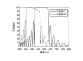
- FIG. 17 is an explanatory diagram showing the wavelength characteristics of reflected excitation light for each twist pitch number of liquid crystal molecules.
- FIG. 18 is an explanatory diagram showing the relationship between the wavelength characteristics of excitation light reflected at an incident angle of 0° to the cholesteric liquid crystal layer and the wavelength characteristics of excitation light reflected at an incident angle of 30° to the cholesteric liquid crystal layer.
- FIG. 19 is an explanatory diagram showing the relationship between the resolution of the cholesteric liquid crystal layer for the excitation light and the incident angle of the excitation light to the cholesteric liquid crystal layer.
- FIG. 20 is an explanatory diagram showing the relationship between the reflectance of excitation light versus the twist pitch number when the incidence angle on the cholesteric liquid crystal layer is 30° and the reflectance of excitation light versus the twist pitch number when the incidence angle on the cholesteric liquid crystal layer is 0°.
- FIG. 21 is a schematic diagram showing a fluorescence detection device according to the fifth embodiment.
- FIG. 22 is a schematic diagram showing a fluorescence detection device according to the sixth embodiment.
- FIG. 23 is a schematic diagram showing a fluorescence detection device according to the seventh embodiment.
- FIG. 24 is a schematic diagram showing a fluorescence detection device according to a second comparative example.
- FIG. 25 is a schematic diagram showing a fluorescence detection device according to the eighth embodiment.
- FIG. 21 is a schematic diagram showing a fluorescence detection device according to the fifth embodiment.
- FIG. 22 is a schematic diagram showing a fluorescence detection device according to the sixth embodiment.
- FIG. 23 is a schematic
- FIG. 26 is a schematic diagram showing another example of the fluorescence detection device according to the eighth embodiment.
- FIG. 27 is a schematic diagram showing a fluorescence detection device according to Comparative Example 3.
- FIG. 28 is a schematic diagram showing a fluorescence detection device according to the ninth embodiment.
- FIG. 29 is a schematic diagram showing a fluorescence detection device according to the tenth embodiment.
- FIG. 30 is a schematic diagram showing another example of the fluorescence detection device according to the tenth embodiment.
- FIG. 31 is a schematic diagram showing a fluorescence detection device according to Comparative Example 4. As shown in FIG.
- the term "on top” is used, unless otherwise specified, to include both a case in which another structure is placed directly on top of a structure so as to be in contact with the structure, and a case in which another structure is placed above a structure via yet another structure.
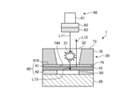
- FIG. 1 is a schematic diagram showing a fluorescence detection device according to the first embodiment.
- FIG. 2 is a cross-sectional view that typically explains the cholesteric liquid crystal layer of the first embodiment.
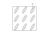
- FIG. 3 is a plan view that typically explains the first and seventh layers of the cholesteric liquid crystal layer of the first embodiment.
- FIG. 4 is a plan view that typically explains the second layer of the cholesteric liquid crystal layer of the first embodiment.
- FIG. 5 is a plan view that typically explains the third layer of the cholesteric liquid crystal layer of the first embodiment.
- FIG. 6 is a plan view that typically explains the fourth layer of the cholesteric liquid crystal layer of the first embodiment.
- FIG. 1 is a schematic diagram showing a fluorescence detection device according to the first embodiment.
- FIG. 2 is a cross-sectional view that typically explains the cholesteric liquid crystal layer of the first embodiment.
- FIG. 3 is a plan view that typically explains the first and seventh layers of the
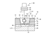
- the fluorescence detection device 1 has a light source 60, a cholesteric liquid crystal layer 10, a light-transmitting substrate 20, a sample holder 30, a resin layer 40, and a sensor 50 in a space that is shielded from light from the outside.
- the fluorescence detection device 1 When the fluorescence detection device 1 irradiates the sample 31 with excitation light L11 of a predetermined wavelength, the substance in the sample 31 is excited and emits fluorescence L13 having spectral characteristics whose peak wavelength is slightly shifted from the wavelength of the excitation light.
- the fluorescence detection device 1 is capable of observing the intensity of this fluorescence L13 and the emission intensity distribution of the fluorescence L13.
- the resin layer 40 is an optical resin having optical transparency, and includes a first resin layer 41 and a second resin layer 42.
- the first resin layer 41 is disposed on the cholesteric liquid crystal layer 10.
- the second resin layer 42 is disposed below the cholesteric liquid crystal layer 10.
- the resin layer 40 is molded integrally with the cholesteric liquid crystal layer 10.
- the light-transmitting substrate 20 is an insulating base material, for example, glass.
- the light-transmitting substrate 20 is disposed below the second resin layer 42.
- the liquid crystal layer 16 is formed on the second resin layer 42 via an alignment film 15.
- the alignment film 15 is made of polyimide or the like, and is subjected to rubbing and photoalignment processes.
- elongated liquid crystal molecules are aligned in one plane with the long axis direction aligned, and the liquid crystal molecules LC rotate in a spiral shape as they move in a direction perpendicular to the plane of the second resin layer 42.
- the first layer LC1, the second layer LC2, the third layer LC3, the fourth layer LC4, the fifth layer LC5, the sixth layer LC6, and the seventh layer LC7 shown in FIG. 2 have liquid crystal molecules LC rotated as shown in FIG. 3 to FIG.
- the long axis direction of the liquid crystal molecules LC is aligned every 1/2 of the pitch p of the spiral, so that the long axis direction of the liquid crystal molecules LC in the first layer LC1 and the long axis direction of the liquid crystal molecules LC in the seventh layer LC7 are in the same direction as shown in FIG. 3.
- the thickness of the liquid crystal molecule LC of the cholesteric liquid crystal layer 10 when it makes one rotation is called the helical pitch p.
- FIG. 9 is an explanatory diagram for explaining the relationship between excitation light and reflected light.
- the cholesteric liquid crystal layer 10 reflects light of a specific wavelength that has circular polarization in the same direction as the rotation direction of the spiral. As shown in FIG. 9, the excitation light L11 incident on the cholesteric liquid crystal layer 10 is reflected according to the same conditions as Bragg's law shown in the following formula (1).
- m is the reflection order
- ⁇ is the reflection wavelength
- p is the helical pitch
- n is the refractive index
- ⁇ is the angle that the incident direction of the excitation light makes with respect to the reflecting surface BL.
- the sample holder 30 includes a light-shielding resin substrate 70 having a first surface 73 and a second surface 74 on the opposite side of the first surface 73, facing the cholesteric liquid crystal layer 10, and a through hole 32 penetrating from the first surface 73 to the second surface 74.
- the opening surface 740 of the through hole 32 on the second surface 74 is blocked by the upper surface 410 of the first resin layer 41.
- the inside of the through hole 32 is filled with an aqueous solution and contains the sample 31.
- the sample holder 30 is located on the upper surface 410 of the first resin layer 41 and is molded integrally with the first resin layer 41.
- the light source 60 includes a light emitter 61, a polarizing plate 62, and a quarter-wave plate 63.
- the light emitter 61 is a light-emitting element that oscillates and emits a predetermined excitation light.
- the polarizing plate 62 makes the light from the light emitter 61 linearly polarized.
- the quarter-wave plate 63 converts the light from the polarizing plate 62 into circularly polarized excitation light L11.
- the sensor 50 is a charge coupled device and an imaging circuit.
- the sensor 50 is embedded in the center of the second resin layer 42.
- the sensor 50 can detect the intensity of the fluorescence and the distribution of the emission intensity of the fluorescence.
- excitation light L11 incident from light source 60 is selectively reflected as reflected light L12.
- the cholesteric liquid crystal layer 10 reflects right-handed circularly polarized light of the excitation light L11 having a wavelength corresponding to the pitch p, and outputs this as reflected light L12.
- the cholesteric liquid crystal layer 10 reflects left-handed circularly polarized light of the excitation light L11 having a wavelength corresponding to the pitch p, and outputs this as reflected light L12.
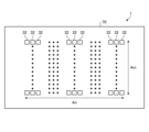
- FIG. 10 is a schematic diagram showing an example of the arrangement of through holes.
- FIG. 11 is a schematic diagram showing the shape of the through holes.
- a plurality of through holes 32 are formed in one resin substrate 70.
- a total of 1250 through holes 32 are provided in one resin substrate 70, 25 in the vertical direction Am and 50 in the horizontal direction An, and are arranged at equal intervals from each other.
- one side 32a of the opening surface 730 of the through hole 32 in the first surface 73 is a square with 650 ⁇ m in size and the other side 32b is 650 ⁇ m in size.
- one side 32c of the opening surface 740 of the through hole 32 in the second surface 74 is a square with 350 ⁇ m in size and the other side 32d is 350 ⁇ m in size.
- the depth 32h of the through hole 32 is 150 ⁇ m.
- the cholesteric liquid crystal layer 10 is manufactured by selecting a liquid crystal material and a chiral agent according to the wavelength of the excitation light L11.
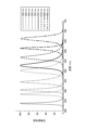
- Figure 12 is a graph showing the emission spectrum of an inorganic LED.
- the wavelength range is about 100 nm, so the wavelength range of the reflected light of the cholesteric liquid crystal layer 10 needs to be at least 50 nm or more.
- the wavelength range of the reflected light from the cholesteric liquid crystal layer 10 is 100 nm or more.
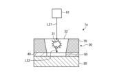
- FIG. 13 is a schematic diagram showing a fluorescence detection device according to Comparative Example 1.
- the fluorescence detection device 1a of Comparative Example 1 shown in FIG. 13 does not have a cholesteric liquid crystal layer 10, unlike the fluorescence detection device 1 shown in FIG. 1.
- the fluorescence detection device 1a of Comparative Example 1 irradiates the sample 31 with excitation light L21 of a predetermined wavelength, the substance in the sample is excited and emits fluorescence having spectral characteristics whose peak wavelength is slightly shifted from the wavelength of the excitation light.
- fluorescence L22 containing noise from the excitation light reaches the sensor 50.
- the cholesteric liquid crystal layer 10 selectively reflects the excitation light L11 as reflected light L12.
- the fluorescence detection device 1 of embodiment 1 includes a light source 60 that irradiates the sample 31 with excitation light L11 in a circularly polarized state, a cholesteric liquid crystal layer 10 that transmits fluorescence L13 emitted by the sample 31 in response to the excitation light L11 and reflects the excitation light L11, and a sensor 50 that detects the fluorescence L13 that has transmitted through the cholesteric liquid crystal layer 10.
- the detection sensitivity of the fluorescence L13 detected by the sensor 50 is improved.
- (Embodiment 2) 14 is a schematic diagram showing a fluorescence detection device according to embodiment 2.
- the same components as those described in the above-mentioned embodiments are denoted by the same reference numerals, and duplicated description will be omitted.
- the fluorescence detection device 1A has a light source 60, a cholesteric liquid crystal layer 10, a light-transmitting substrate 20, a sample holder 30, a resin layer 40, and a sensor 50 in a space shielded from external light.
- the angle between the second surface 74 and the side wall 75 of the through hole 32 is 45° or more, when the excitation light L11 from the light source 60 is refracted at the side wall 75, the direction of the circular polarization state of the reflected light L12 is reversed, and the reflected light L12 is likely to be incident on the sensor 50. Because the direction in which the liquid crystal molecules LC in the cholesteric liquid crystal layer 10 rotate is opposite to the direction of the circular polarization state of the reflected light L12, the cholesteric liquid crystal layer 10 cannot reflect the reflected light L12, and there is a possibility that the fluorescence L22 containing the noise of the excitation light L11 will reach the sensor 50.
- the area of the opening surface 730 is larger than the area of the opening surface 740, is tapered, and the angle between the second surface 74 and the side wall 75 is set to 45° or less.
- the fluorescence detection device 1A reflects the excitation light L11 as reflected light L14, and can prevent the excitation light L11 from entering the sensor 50.
- (Embodiment 3) 15 is a schematic diagram showing a fluorescence detection device according to embodiment 3.
- the same components as those described in the above embodiments are denoted by the same reference numerals, and duplicated description will be omitted.
- the fluorescence detection device 1B has a light source 60, a cholesteric liquid crystal layer 10, a light-transmitting substrate 20, a sample holder 30, a resin layer 40, and a sensor 50 in a space shielded from light from the outside.
- the cholesteric liquid crystal layer 10 of the third embodiment has liquid crystal molecules LC that rotate in a spiral shape, and includes a first liquid crystal layer 11 and a second liquid crystal layer 12 that rotates in a direction different from that of the liquid crystal molecules LC of the first liquid crystal layer 11.
- the first liquid crystal layer 11 has left-handed liquid crystal molecules LC, and is formed on the second liquid crystal layer 12.
- the second liquid crystal layer 12 has right-handed liquid crystal molecules LC, and is formed on an alignment film 15.
- the cholesteric liquid crystal layer 10 may include three or more liquid crystal layers that rotate in a direction different from that of the liquid crystal molecules.
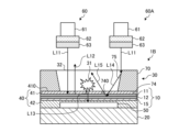
- the excitation light L11 is reflected as reflected light L14, and the excitation light L11 can be prevented from entering the sensor 50.
- the fluorescence detection device 1B of embodiment 3 even if the angle between the second surface 74 and the side wall 75 is 45° or more, the reflected light L14 can be prevented from entering the sensor 50.
- the second liquid crystal layer 12 having liquid crystal molecules LC that rotate in a direction different from the direction in which the liquid crystal molecules LC of the first liquid crystal layer 11 rotate is laminated on the first liquid crystal layer 11.
- the first liquid crystal layer 11 reflects the excitation light L11.
- the first liquid crystal layer 11 cannot reflect the reflected light L14 of the light source 60A. This is because the direction in which the liquid crystal molecules LC of the first liquid crystal layer 11 rotate is opposite to the direction of the circular polarization state of the reflected light L12.
- the reflected light L14 reaches the second liquid crystal layer 12. Because the direction in which the liquid crystal molecules LC of the second liquid crystal layer 12 rotate is the same as the direction of the circular polarization state of the reflected light L12, the second liquid crystal layer 12 can reflect the reflected light L14 as reflected light L15.
- FIG. 16 is a schematic diagram showing a fluorescence detection device according to the fourth embodiment.
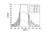
- FIG. 17 is an explanatory diagram showing the wavelength characteristics of the reflected excitation light for each twist pitch number of the liquid crystal molecules.
- FIG. 18 is an explanatory diagram showing the relationship between the wavelength characteristics of the reflected excitation light at an incident angle of 0° to the cholesteric liquid crystal layer and the wavelength characteristics of the reflected excitation light at an incident angle of 30° to the cholesteric liquid crystal layer.
- FIG. 19 is an explanatory diagram showing the relationship between the resolution of the cholesteric liquid crystal layer for the excitation light and the incident angle of the excitation light to the cholesteric liquid crystal layer.
- FIG. 20 is an explanatory diagram showing the relationship between the reflectance of the excitation light with respect to the twist pitch number at an incident angle of 30° to the cholesteric liquid crystal layer and the reflectance of the excitation light with respect to the twist pitch number at an incident angle of 0° to the cholesteric liquid crystal layer.
- the same components as those described in the above-mentioned embodiment are given the same reference numerals, and duplicated description will be omitted.
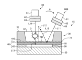
- the fluorescence detection device 1C has a light source 60, a cholesteric liquid crystal layer 10, a light-transmitting substrate 20, a sample holder 30, a resin layer 40, and a sensor 50 in a space shielded from external light.
- the number of helical pitches contained in the thickness of the cholesteric liquid crystal layer 10 is called the pitch number. As shown in Figure 17, when the pitch number is 5 pitches or less, the reflectance of the cholesteric liquid crystal layer 10 tends to decrease.
- the pitch number is preferably 5 pitches or more, and more preferably 10 pitches or more.
- the incident angle the angle at which the excitation light L11 is incident on the surface of the cholesteric liquid crystal layer 10
- the central wavelength of the cholesteric liquid crystal layer 10 shifts when the incident angle is 30°.
- the angle of incidence is 30° or more, there is a possibility that the fluorescence L22 containing the noise of the excitation light L11 may reach the sensor 50.
- the reflectance of the excitation light L11 and the resolution for the excitation light L11 can be maintained by setting the incident angle to 30° or less.
- the angle of incidence is 30° or less. As shown in FIG. 19, when the angle of incidence is 20°, 100% of the resolution can be maintained compared to when the angle of incidence is 30°, so an angle of incidence of 20° or less is more preferable.
- the incident angle when the incident angle is 0° and the pitch number is more than 5 and is equal to or greater than 10, the reflectance of the cholesteric liquid crystal layer 10 can be maintained at 100% even if the pitch number increases.
- the incident angle when the incident angle is 30° and the pitch number is more than 5 and is equal to or greater than 10, the reflectance of the cholesteric liquid crystal layer 10 can be maintained at 93% even if the pitch number increases.
- the incident angle is 30° and the pitch number is less than 10 pitches, the reflectance of the cholesteric liquid crystal layer 10 decreases. Therefore, in order to suppress the decrease in the reflectance of the cholesteric liquid crystal layer 10 even if the incident angle changes, the incident angle is preferably 30° or less and the pitch number is preferably 10 pitches or more.
- the fluorescence detection device 1C suppresses the shift in the center wavelength of the cholesteric liquid crystal layer 10 and the decrease in reflectance, and increases the ability of the cholesteric liquid crystal layer 10 to resolve circularly polarized light.
- (Embodiment 5) 21 is a schematic diagram showing a fluorescence detection device according to embodiment 5.
- the same components as those described in the above embodiments are denoted by the same reference numerals, and duplicated description will be omitted.
- the fluorescence detection device 1D has a light source 60, a cholesteric liquid crystal layer 10, a light-transmitting substrate 20, a sample holder 30, a resin layer 40, a sensor 50, and a light-shielding layer 71 in a space that is shielded from external light.
- the light-transmitting substrate 20 has a first light-transmitting substrate 21 and a second light-transmitting substrate 22.
- the resin layer 40 is placed on the second light-transmitting substrate 22.
- the sensor 50 is embedded in the center of the resin layer 40.
- the outer periphery of the upper surface 51 of the sensor 50 is surrounded by a light-shielding layer 71.
- the cholesteric liquid crystal layer 10 is formed by depositing a liquid crystal layer 16 on the resin layer 40 with an alignment film 15 interposed therebetween.
- the first light-transmitting substrate 21 is disposed on the cholesteric liquid crystal layer 10.
- the sample holder 30 is molded integrally with the first resin layer 41 provided on the cholesteric liquid crystal layer 10, and the opening surface 740 is covered by the upper surface 410 of the first resin layer 41.
- the opening surface 740 is covered by the upper surface 210 of the first light-transmissive substrate 21.
- the first light-transmissive substrate 21 has a higher solvent resistance than resin, the degree of freedom of the solvent that enters the through-hole 32 is increased.
- the light-shielding layer 71 blocks stray light entering the sensor 50 and suppresses light scattering in the first light-transmissive substrate 21, thereby improving the detection accuracy of the sensor 50.
- (Embodiment 6) 22 is a schematic diagram showing a fluorescence detection device according to embodiment 6.
- the same components as those described in the above embodiments are denoted by the same reference numerals, and duplicated description will be omitted.
- the fluorescence detection device 1E has a light source 60, a cholesteric liquid crystal layer 10, a light-transmitting substrate 20, a sample holder 30, a resin layer 40, and a sensor 50 in a space that is shielded from external light.
- the resin layer 40 is placed on the light-transmitting substrate 20.
- the sensor 50 is embedded in the center of the resin layer 40.
- the upper surface 51 of the sensor 50 is exposed and is positioned to match the opening surface 740.
- the cholesteric liquid crystal layer 10 is placed on the upper surface 51 of the sensor 50, and the liquid crystal layer 16 is formed on the resin layer 40 via an alignment film 15.
- the alignment film 15 covers the first surface 73 of the sample holder 30, the side wall 75, and the upper surface 51 of the sensor 50.
- the fluorescence detection device 1E simplifies the manufacturing process of the fluorescence detection device because the cholesteric liquid crystal layer 10 is formed inside the through-hole 32.
- the excitation light L11 enters the cholesteric liquid crystal layer 10 via the first resin layer 41.
- the excitation light L11 is incident directly on the cholesteric liquid crystal layer 10 without passing through a resin layer, so noise in the excitation light L11 can be further suppressed, thereby improving the detection accuracy of the sensor 50.
- (Embodiment 7) 23 is a schematic diagram showing a fluorescence detection device according to embodiment 7.
- the same components as those described in the above embodiments are denoted by the same reference numerals, and duplicated description will be omitted.
- the fluorescence detection device 1F has a light source 60, a cholesteric liquid crystal layer 10, a light-transmitting substrate 20, a sample holder 30, a resin layer 40, and a sensor 50 in a space shielded from external light.
- the sample holder 30 includes a light-shielding resin substrate 70 having a first surface 73 and a second surface 74 on the opposite side of the first surface 73, facing the cholesteric liquid crystal layer 10, and a through hole 32 that penetrates from the first surface 73 to the second surface 74.
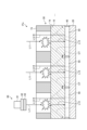
- a plurality of storage sections 300 for storing samples 31 are arranged within a single resin substrate 70, each surrounded by a side wall 75 of a through hole 32.
- the storage sections 300 are arranged on the cholesteric liquid crystal layer 10.
- the inside of the storage section 300 is filled with an aqueous solution, and the sample 31 is stored therein.
- the resin layer 40 is placed on the light-transmitting substrate 20.
- the sensor 50 is embedded in the center of the resin layer 40.
- the upper surface 51 of the sensor 50 is exposed.
- the cholesteric liquid crystal layer 10 is disposed on the upper surface 51 of the sensor 50, and the liquid crystal layer 16 is formed on the resin layer 40 via an alignment film 15.
- the outside of the cholesteric liquid crystal layer 10 is surrounded by a side wall 75.
- the sensors 50 are disposed adjacent to each other in the horizontal direction.
- FIG. 24 is a schematic diagram showing a fluorescence detection device according to Comparative Example 2.
- the fluorescence detection device 1Fa of Comparative Example 2 shown in FIG. 24 is different from the fluorescence detection device 1F shown in FIG. 23 in that multiple cholesteric liquid crystal layers 10 are arranged for each storage section 300, and the exterior of the cholesteric liquid crystal layer 10 is not surrounded by a resin substrate 70.
- the thickness of the cholesteric liquid crystal layer 10 needs to be greater than the thickness of the storage section 300.
- the fluorescence detection device 1Fa of Comparative Example 2 the fluorescence L13 that should enter one of the adjacent sensors 50 enters the other sensor 50, causing mutual interference between the adjacent sensors 50, known as crosstalk CT, and reducing the light receiving sensitivity.
- the cholesteric liquid crystal layer 10 is surrounded by a resin substrate 70 for each storage section 300, and the space between the cholesteric liquid crystal layers 10 is shielded from light, thereby preventing the fluorescence L13 that should enter one sensor 50 from entering the other sensor 50.
- Fig. 25 is a schematic diagram showing a fluorescence detection device according to embodiment 8.
- Fig. 26 is a schematic diagram showing another example of a fluorescence detection device according to embodiment 8.
- the same components as those described in the above-mentioned embodiments are denoted by the same reference numerals, and duplicated description will be omitted.
- the fluorescence detection device 1G has a light source 60, a cholesteric liquid crystal layer 10, a light-transmitting substrate 20, a sample holder 30, a resin layer 40, and a sensor 50 in a space shielded from external light.
- the cholesteric liquid crystal layer 10 includes a first liquid crystal layer 11 and a second liquid crystal layer 12.
- the angle of incidence ⁇ 1 of the excitation light L11 with respect to the side wall 75 is 45°, a critical angle at which the excitation light L11 does not critically enter the sensor 50 directly, and the inside of the storage section 300 is divided into an exposed area AA and an unexposed area AB.
- the configuration of the fluorescence detection device 1G' shown in FIG. 26 is the same as that of the fluorescence detection device 1G.
- the incident angle ⁇ 1 of the excitation light L11 with respect to the side wall 75 is equal to or greater than the critical angle of 45°, so that the inside of the storage section 300 is divided into an exposed area AA and a non-exposed area AB.
- FIG. 27 is a schematic diagram showing a fluorescence detection device according to Comparative Example 3.
- a fluorescence detection device 1Ga of Comparative Example 3 shown in FIG. 27 a portion of the upper surface 110 is exposed to the exposure area AA, as compared to the fluorescence detection devices 1G and 1G' shown in FIGS. 25 and 26.
- the incident angle ⁇ 1 of the excitation light L11 with respect to the side wall 75 is less than the critical angle of 45°, so that a portion of the upper surface 110 where the fluorescence L13 enters the cholesteric liquid crystal layer 10 is exposed to the exposure area AA, and the amount of excitation light L11 that directly enters the sensor 50 increases.
- the entire upper surface 110 faces the exposure area AA, so that the excitation light L11 can be incident only on the sample 31, preventing the excitation light L11 from directly entering the sensor 50 and reducing the amount of excitation light L11 that enters.
- the fluorescence detection device 1G (Fig. 25) and the fluorescence detection device 1G' (Fig. 26) are examples of devices in which the aspect ratio (width to height ratio) of the side wall 75 and the top surface 110 is 1:1, and the critical angle of the incidence angle ⁇ 1 is 45°. If the aspect ratio (width to height ratio) of the fluorescence detection device is different, the critical angle of the incidence angle ⁇ 1 will be changed appropriately depending on the aspect ratio.
- the critical angle of the incident angle ⁇ 1 is 30°. If the incident angle ⁇ 1 is less than the critical angle of 30°, a portion of the top surface 110 where the fluorescence L13 enters the cholesteric liquid crystal layer 10 is exposed to the exposure area AA, and the amount of excitation light L11 that directly enters the sensor 50 increases.
- the entire upper surface 110 faces the exposure area AA, so that the excitation light L11 can be incident only on the sample 31, preventing the excitation light L11 from directly entering the sensor 50 and reducing the amount of excitation light L11 that enters.
- (Embodiment 9) 28 is a schematic diagram showing a fluorescence detection device according to embodiment 9.
- the same components as those described in the above embodiments are denoted by the same reference numerals, and duplicated description will be omitted.
- the upper surface 110 of the cholesteric liquid crystal layer 10 facing the non-exposed region AB and the upper surface 51 of the sensor 50 are inclined toward the side wall 75 so as to be parallel to the light beam of the excitation light L11.
- the distance that the excitation light L11 travels before reflecting off the side wall 75 and penetrating the upper surface 51 of the sensor 50 where the light is incident is increased, so that the excitation light L11 can be prevented from directly penetrating the sensor 50 even more effectively than in the fluorescence detection device 1G of embodiment 8.
- Fig. 29 is a schematic diagram showing a fluorescence detection device according to embodiment 10.
- Fig. 30 is a schematic diagram showing another example of a fluorescence detection device according to embodiment 10.
- the same components as those described in the above embodiments are denoted by the same reference numerals, and duplicated description will be omitted.
- the configuration of the fluorescence detection device 1I shown in FIG. 29 and the configuration of the fluorescence detection device 1I' shown in FIG. 30 are the same as those of the fluorescence detection device 1B.
- the incident angle ⁇ 1 of the excitation light L11 with respect to the side wall 75 is a critical angle of 45°, so that the inside of the through hole 32 is divided into an exposed area AA and a non-exposed area AB.
- the entire surface of the opening surface 740 faces the non-exposed area AB.
- the incident angle ⁇ 1 of the excitation light L11 with respect to the side wall 75 is equal to or greater than the critical angle of 45°, so that the inside of the through hole 32 is divided into an exposed area AA and a non-exposed area AB.
- the entire opening surface 740 faces the non-exposed area AB.
- FIG. 31 is a schematic diagram showing a fluorescence detection device according to Comparative Example 4.
- a fluorescence detection device 1Ia of Comparative Example 4 shown in FIG. 31 a part of the opening surface 740 is exposed to the exposure area AA, as compared to the fluorescence detection devices 1I and 1I' shown in FIGS. 29 and 30.
- the incident angle ⁇ 1 of the excitation light L11 with respect to the side wall 75 is less than the critical angle of 45°, so that a portion of the opening surface 740 is exposed to the exposure area AA, and a large amount of the excitation light L11 enters the sensor 50 directly.
- the entire surface of the opening surface 740 faces the exposure area AA, so that the excitation light L11 can be incident only on the sample 31, preventing the excitation light L11 from directly entering the sensor 50 and reducing the amount of excitation light L11 that enters.
- the fluorescence detection device 1I (Fig. 29) and the fluorescence detection device 1I' (Fig. 30) are examples of devices in which the aspect ratio (horizontal to vertical ratio) of the side wall 75 and the opening surface 740 is 1:1, and the critical angle of the incidence angle ⁇ 1 is 45°. If the aspect ratio (horizontal to vertical ratio) of the fluorescence detection device is different, the critical angle of the incidence angle ⁇ 1 will be changed appropriately depending on the aspect ratio.
- the critical angle of the incident angle ⁇ 1 is 30°. If the incident angle ⁇ 1 is less than the critical angle of 30°, a portion of the opening surface 740 where the fluorescence L13 enters the cholesteric liquid crystal layer 10 is exposed to the exposure area AA, and the amount of excitation light L11 that directly enters the sensor 50 increases.
- the incident angle ⁇ 1 is equal to or greater than the critical angle of 30°
- the entire surface of the opening 740 faces the exposure area AA, so that the excitation light L11 can be incident only on the sample 31, preventing the excitation light L11 from directly entering the sensor 50 and reducing the amount of excitation light L11 that enters.
Landscapes
- Physics & Mathematics (AREA)
- Nonlinear Science (AREA)
- General Physics & Mathematics (AREA)
- Chemical & Material Sciences (AREA)
- Health & Medical Sciences (AREA)
- Optics & Photonics (AREA)
- Mathematical Physics (AREA)
- Crystallography & Structural Chemistry (AREA)
- Analytical Chemistry (AREA)
- Biochemistry (AREA)
- General Health & Medical Sciences (AREA)
- Life Sciences & Earth Sciences (AREA)
- Immunology (AREA)
- Pathology (AREA)
- Nuclear Medicine, Radiotherapy & Molecular Imaging (AREA)
- Investigating, Analyzing Materials By Fluorescence Or Luminescence (AREA)
Priority Applications (2)
| Application Number | Priority Date | Filing Date | Title |
|---|---|---|---|
| JP2024555856A JPWO2024075814A1 (https=) | 2022-10-05 | 2023-10-05 | |
| US19/096,998 US20250231111A1 (en) | 2022-10-05 | 2025-04-01 | Fluorescence detection device |
Applications Claiming Priority (2)
| Application Number | Priority Date | Filing Date | Title |
|---|---|---|---|
| JP2022160919 | 2022-10-05 | ||
| JP2022-160919 | 2022-10-05 |
Related Child Applications (1)
| Application Number | Title | Priority Date | Filing Date |
|---|---|---|---|
| US19/096,998 Continuation US20250231111A1 (en) | 2022-10-05 | 2025-04-01 | Fluorescence detection device |
Publications (1)
| Publication Number | Publication Date |
|---|---|
| WO2024075814A1 true WO2024075814A1 (ja) | 2024-04-11 |
Family
ID=90608440
Family Applications (1)
| Application Number | Title | Priority Date | Filing Date |
|---|---|---|---|
| PCT/JP2023/036355 Ceased WO2024075814A1 (ja) | 2022-10-05 | 2023-10-05 | 蛍光検出装置 |
Country Status (3)
| Country | Link |
|---|---|
| US (1) | US20250231111A1 (https=) |
| JP (1) | JPWO2024075814A1 (https=) |
| WO (1) | WO2024075814A1 (https=) |
Families Citing this family (1)
| Publication number | Priority date | Publication date | Assignee | Title |
|---|---|---|---|---|
| CN121115358B (zh) * | 2025-11-17 | 2026-04-14 | 惠科股份有限公司 | 反射式显示装置和反射式显示装置的制备方法 |
Citations (9)
| Publication number | Priority date | Publication date | Assignee | Title |
|---|---|---|---|---|
| JP2004004764A (ja) * | 2002-04-24 | 2004-01-08 | Nitto Denko Corp | 集光システムおよび透過型液晶表示装置 |
| US20110085219A1 (en) * | 2009-10-13 | 2011-04-14 | California Institute Of Technology | Holographically Illuminated Imaging Devices |
| US20120305801A1 (en) * | 2011-05-31 | 2012-12-06 | Samsung Electronics Co., Ltd. | Fluorescence detecting optical system and multi-channel fluorescence detection apparatus having the same |
| JP2016061833A (ja) * | 2014-09-16 | 2016-04-25 | 富士フイルム株式会社 | 発光スクリーン、表示装置 |
| JP2017161793A (ja) * | 2016-03-10 | 2017-09-14 | シスメックス株式会社 | 光学機器、位相板および像の形成方法 |
| CN108535911A (zh) * | 2018-05-21 | 2018-09-14 | 京东方科技集团股份有限公司 | 一种透明液晶显示装置 |
| WO2020230556A1 (ja) * | 2019-05-10 | 2020-11-19 | 富士フイルム株式会社 | センサー |
| WO2020230698A1 (ja) * | 2019-05-10 | 2020-11-19 | 富士フイルム株式会社 | センサー |
| WO2023038053A1 (ja) * | 2021-09-10 | 2023-03-16 | 富士フイルム株式会社 | 液晶表示装置 |
-
2023
- 2023-10-05 JP JP2024555856A patent/JPWO2024075814A1/ja active Pending
- 2023-10-05 WO PCT/JP2023/036355 patent/WO2024075814A1/ja not_active Ceased
-
2025
- 2025-04-01 US US19/096,998 patent/US20250231111A1/en active Pending
Patent Citations (9)
| Publication number | Priority date | Publication date | Assignee | Title |
|---|---|---|---|---|
| JP2004004764A (ja) * | 2002-04-24 | 2004-01-08 | Nitto Denko Corp | 集光システムおよび透過型液晶表示装置 |
| US20110085219A1 (en) * | 2009-10-13 | 2011-04-14 | California Institute Of Technology | Holographically Illuminated Imaging Devices |
| US20120305801A1 (en) * | 2011-05-31 | 2012-12-06 | Samsung Electronics Co., Ltd. | Fluorescence detecting optical system and multi-channel fluorescence detection apparatus having the same |
| JP2016061833A (ja) * | 2014-09-16 | 2016-04-25 | 富士フイルム株式会社 | 発光スクリーン、表示装置 |
| JP2017161793A (ja) * | 2016-03-10 | 2017-09-14 | シスメックス株式会社 | 光学機器、位相板および像の形成方法 |
| CN108535911A (zh) * | 2018-05-21 | 2018-09-14 | 京东方科技集团股份有限公司 | 一种透明液晶显示装置 |
| WO2020230556A1 (ja) * | 2019-05-10 | 2020-11-19 | 富士フイルム株式会社 | センサー |
| WO2020230698A1 (ja) * | 2019-05-10 | 2020-11-19 | 富士フイルム株式会社 | センサー |
| WO2023038053A1 (ja) * | 2021-09-10 | 2023-03-16 | 富士フイルム株式会社 | 液晶表示装置 |
Also Published As
| Publication number | Publication date |
|---|---|
| US20250231111A1 (en) | 2025-07-17 |
| JPWO2024075814A1 (https=) | 2024-04-11 |
Similar Documents
| Publication | Publication Date | Title |
|---|---|---|
| KR102233732B1 (ko) | 분광 장치 및 분광 방법 | |
| TWI503532B (zh) | 臨界角光學感測器設備 | |
| WO2024075814A1 (ja) | 蛍光検出装置 | |
| EP0981734B1 (en) | Fluorescence sensing device | |
| JPWO2024075814A5 (https=) | ||
| ES3055651T3 (en) | Detection chip, detection system, and detection method | |
| US10337994B2 (en) | Sample liquid measuring device and measuring method | |
| US8704154B2 (en) | Non-contact probe with an optical filter and measuring machine including the same | |
| CN100533125C (zh) | 荧光测定装置 | |
| JP2014032148A (ja) | 表面プラズモン励起増強蛍光取得構造体および表面プラズモン励起増強蛍光測定システム | |
| US11169090B2 (en) | Diffracted light removal slit and optical sample detection system using same | |
| US7843570B2 (en) | Crystal oscillator sensor and substance adsorption detection method using the sensor | |
| US20070247623A1 (en) | Polarization measuring devices, ellipsometers and polarization measuring methods | |
| JP2015078904A (ja) | 光学素子、分析装置、及び電子機器 | |
| WO2017082196A1 (ja) | 検査チップおよび検査システム | |
| WO2018229477A1 (en) | Reading device for a lateral flow test strip | |
| US7718952B2 (en) | Information carrier | |
| JPWO2024009737A5 (https=) | ||
| WO2024009737A1 (ja) | 蛍光検出装置 | |
| KR20210038756A (ko) | 표시 장치 | |
| Gust et al. | Unexpected Sign Inversion of the Circular Dichroism and Circularly Polarized Luminescence Response of Chiral Copolymer Thin Films by Tuning the Thickness and Annealing Conditions | |
| US20060060931A1 (en) | Standard micro-component for calibrating or standardizing fluorescence measuring instruments and biochip comprising same | |
| US10989859B2 (en) | Backlight unit and display apparatus including the same | |
| JP2007059770A5 (https=) | ||
| TWI858877B (zh) | 螢光生物感測系統和生物偵測方法 |
Legal Events
| Date | Code | Title | Description |
|---|---|---|---|
| 121 | Ep: the epo has been informed by wipo that ep was designated in this application |
Ref document number: 23874939 Country of ref document: EP Kind code of ref document: A1 |
|
| WWE | Wipo information: entry into national phase |
Ref document number: 2024555856 Country of ref document: JP |
|
| NENP | Non-entry into the national phase |
Ref country code: DE |
|
| 122 | Ep: pct application non-entry in european phase |
Ref document number: 23874939 Country of ref document: EP Kind code of ref document: A1 |