WO2024075405A1 - 固体撮像装置 - Google Patents
固体撮像装置 Download PDFInfo
- Publication number
- WO2024075405A1 WO2024075405A1 PCT/JP2023/029670 JP2023029670W WO2024075405A1 WO 2024075405 A1 WO2024075405 A1 WO 2024075405A1 JP 2023029670 W JP2023029670 W JP 2023029670W WO 2024075405 A1 WO2024075405 A1 WO 2024075405A1
- Authority
- WO
- WIPO (PCT)
- Prior art keywords
- pixel
- solid
- state imaging
- imaging device
- gate electrode
- Prior art date
- Legal status (The legal status is an assumption and is not a legal conclusion. Google has not performed a legal analysis and makes no representation as to the accuracy of the status listed.)
- Ceased
Links
Images
































Classifications
-
- H—ELECTRICITY
- H10—SEMICONDUCTOR DEVICES; ELECTRIC SOLID-STATE DEVICES NOT OTHERWISE PROVIDED FOR
- H10F—INORGANIC SEMICONDUCTOR DEVICES SENSITIVE TO INFRARED RADIATION, LIGHT, ELECTROMAGNETIC RADIATION OF SHORTER WAVELENGTH OR CORPUSCULAR RADIATION
- H10F39/00—Integrated devices, or assemblies of multiple devices, comprising at least one element covered by group H10F30/00, e.g. radiation detectors comprising photodiode arrays
- H10F39/80—Constructional details of image sensors
- H10F39/803—Pixels having integrated switching, control, storage or amplification elements
- H10F39/8037—Pixels having integrated switching, control, storage or amplification elements the integrated elements comprising a transistor
- H10F39/80373—Pixels having integrated switching, control, storage or amplification elements the integrated elements comprising a transistor characterised by the gate of the transistor
-
- H—ELECTRICITY
- H10—SEMICONDUCTOR DEVICES; ELECTRIC SOLID-STATE DEVICES NOT OTHERWISE PROVIDED FOR
- H10F—INORGANIC SEMICONDUCTOR DEVICES SENSITIVE TO INFRARED RADIATION, LIGHT, ELECTROMAGNETIC RADIATION OF SHORTER WAVELENGTH OR CORPUSCULAR RADIATION
- H10F39/00—Integrated devices, or assemblies of multiple devices, comprising at least one element covered by group H10F30/00, e.g. radiation detectors comprising photodiode arrays
- H10F39/10—Integrated devices
- H10F39/12—Image sensors
-
- H—ELECTRICITY
- H10—SEMICONDUCTOR DEVICES; ELECTRIC SOLID-STATE DEVICES NOT OTHERWISE PROVIDED FOR
- H10F—INORGANIC SEMICONDUCTOR DEVICES SENSITIVE TO INFRARED RADIATION, LIGHT, ELECTROMAGNETIC RADIATION OF SHORTER WAVELENGTH OR CORPUSCULAR RADIATION
- H10F39/00—Integrated devices, or assemblies of multiple devices, comprising at least one element covered by group H10F30/00, e.g. radiation detectors comprising photodiode arrays
- H10F39/80—Constructional details of image sensors
- H10F39/807—Pixel isolation structures
Definitions
- This disclosure relates to a solid-state imaging device.
- Patent Document 1 discloses a solid-state imaging device.
- the solid-state imaging device has a photoelectric conversion section for each of a number of regularly arranged pixels.
- charge is generated as a signal from incident light.
- the signal is transferred to a floating diffusion via a transfer transistor arranged for each pixel.
- the floating diffusion transfers the signal to a pixel circuit, where the signal is processed.
- the floating diffusion is shared by a number of pixels arranged adjacently.
- Patent Document 1 WO2020-262643
- misalignment occurs in the floating diffusion with respect to the gate electrodes of the transfer transistors of each of the multiple pixels, more specifically, with respect to the connection parts that supply control signals to the gate electrodes.
- This misalignment causes variation in the parasitic capacitance generated between the shared connection parts of each pixel and the floating diffusion. For this reason, it is desirable to improve the signal variation and delay associated with parasitic capacitance in solid-state imaging devices.
- the solid-state imaging device comprises a first pixel disposed on the first surface side of the substrate, which is the light incident side, and having a first photoelectric conversion element that converts light into an electric charge; a first transistor disposed on the second surface side of the substrate opposite the first surface at a position corresponding to the first pixel, having a first gate electrode, and one of a pair of main electrodes electrically connected to the first photoelectric conversion element; a floating diffusion disposed on the second surface side of the substrate and electrically connected to the other main electrode of the first transistor; and a low dielectric constant region disposed between the floating diffusion and the first gate electrode facing it, and having a dielectric constant lower than that of the non-facing region.
- the solid-state imaging device further comprises, in the solid-state imaging device according to the first embodiment, a second pixel disposed adjacent to the first pixel on the first surface side of the substrate and having a second photoelectric conversion element that converts light into an electric charge, a second transistor disposed on the second surface side of the substrate at a position corresponding to the second pixel and having a second gate electrode, one of a pair of main electrodes being electrically connected to the second photoelectric conversion element and the other main electrode being electrically connected to a floating diffusion, and a low dielectric constant region disposed between the floating diffusion and the second gate electrode facing it.
- the low dielectric constant region in the solid-state imaging device according to the first or second embodiment is a gap.
- the low dielectric constant region in the solid-state imaging device according to the first or second embodiment is formed from a low dielectric constant material.
- FIG. 1 is a circuit diagram showing a pixel and a pixel circuit of a solid-state imaging device according to a first embodiment of the present disclosure.
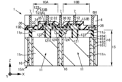
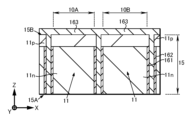
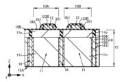
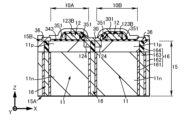
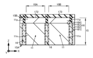
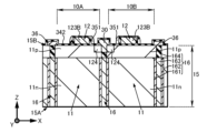
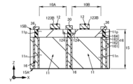
- FIG. 2 is a vertical cross-sectional configuration diagram of the pixel shown in FIG. 1 (a cross-sectional view taken along the line AA shown in FIG. 3).
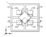
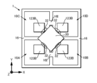
- FIG. 3 is a plan view showing the configuration of the pixel shown in FIG. 4A to 4C are cross-sectional views illustrating a first step of the method for manufacturing the solid-state imaging device according to the first embodiment.
- FIG. 5 is a cross-sectional view of the second process.
- FIG. 6 is a cross-sectional view of the third process.
- FIG. 7 is a cross-sectional view of the fourth step.
- FIG. 1 is a circuit diagram showing a pixel and a pixel circuit of a solid-state imaging device according to a first embodiment of the present disclosure.
- FIG. 2 is a vertical cross-sectional configuration diagram of the pixel shown in FIG. 1
- FIG. 8 is a cross-sectional view of the fifth step.
- FIG. 9 is a cross-sectional view of the sixth step.
- FIG. 10 is a cross-sectional view of the seventh step.
- FIG. 11 is a cross-sectional view of the eighth step.
- FIG. 12 is a cross-sectional view of the ninth step.
- FIG. 13 is a cross-sectional view of the tenth step.
- FIG. 14 is a cross-sectional view of the eleventh step.
- FIG. 15 is a cross-sectional view of the twelfth step.
- FIG. 16 is a cross-sectional view of the thirteenth step.
- FIG. 17 is a cross-sectional view of the fourteenth step.
- FIG. 18 is a cross-sectional view of the 15th step.
- FIG. 19 is a cross-sectional view of the 16th step.
- FIG. 20 is a cross-sectional view of the 17th step.
- FIG. 21 is a cross-sectional view of the 18th step.
- FIG. 22 is a cross-sectional view of the 19th step.
- FIG. 23 is a cross-sectional view of the twentieth step.
- FIG. 24 is a cross-sectional view of the 21st step.
- FIG. 25 is a cross-sectional view of the 22nd step.
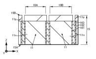
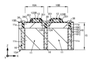
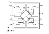
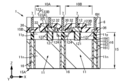
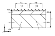
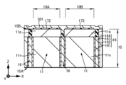
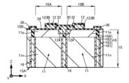
- FIG. 26 is a vertical cross-sectional configuration diagram (a cross-sectional view taken along the line BB shown in FIG. 27) of a pixel of a solid-state imaging device according to the second embodiment of the present disclosure, corresponding to FIG. FIG.
- FIG. 27 is a plan view of the pixel shown in FIG. 26, which corresponds to FIG.
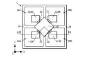
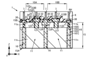
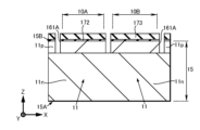
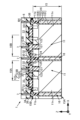
- FIG. 28 is a vertical cross-sectional configuration diagram (a cross-sectional view taken along the CC cutting line shown in FIG. 29) of a pixel of a solid-state imaging device according to a third embodiment of the present disclosure, corresponding to FIG.
- FIG. 29 is a plan view of the pixel shown in FIG. 28, corresponding to FIG.
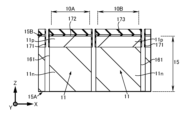
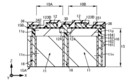
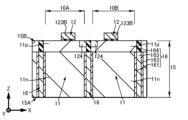
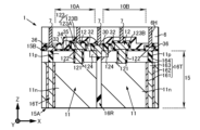
- FIG. 30 is a vertical cross-sectional configuration diagram (a cross-sectional view taken along the line DD shown in FIG. 31) of a pixel of a solid-state imaging device according to a fourth embodiment of the present disclosure, corresponding to FIG.
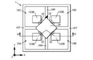
- FIG. 31 is a plan view of the pixel shown in FIG. 30, corresponding to FIG. FIG.
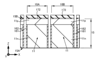
- FIG. 32 is a vertical cross-sectional configuration diagram (a cross-sectional view taken along the line E-E shown in FIG. 33) of a pixel of a solid-state imaging device according to a fifth embodiment of the present disclosure, corresponding to FIG. 2.
- FIG. 33 is a plan view of the pixel shown in FIG. 32, corresponding to FIG.
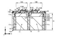
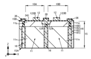
- FIG. 34 is a vertical cross-sectional configuration diagram (a cross-sectional view taken along the line FF shown in FIG. 35) of a pixel of a solid-state imaging device according to a sixth embodiment of the present disclosure, corresponding to FIG. 2.
- FIG. 35 is a plan view of the pixel shown in FIG. 34, corresponding to FIG. FIG.
- FIG. 36 is a cross-sectional view illustrating a first step for explaining each step of a method for manufacturing a solid-state imaging device according to the sixth embodiment.
- FIG. 37 is a cross-sectional view of the second process.
- FIG. 38 is a cross-sectional view of the third step.
- FIG. 39 is a cross-sectional view of the fourth step.
- FIG. 40 is a cross-sectional view of the fifth step.
- FIG. 41 is a cross-sectional view of the sixth step.
- FIG. 42 is a cross-sectional view of the seventh step.
- FIG. 43 is a cross-sectional view of the eighth step.
- FIG. 44 is a cross-sectional view of the ninth step.
- FIG. 45 is a cross-sectional view of the tenth step.
- FIG. 45 is a cross-sectional view of the tenth step.
- FIG. 46 is a cross-sectional view of the 11th step.
- FIG. 47 is a cross-sectional view of the twelfth step.
- FIG. 48 is a cross-sectional view of the thirteenth step.
- FIG. 49 is a cross-sectional view of the 14th step.
- FIG. 50 is a cross-sectional view of the 15th step.
- FIG. 51 is a cross-sectional view of the 16th step.
- FIG. 52 is a cross-sectional view of the 17th step.
- FIG. 53 is a cross-sectional view of the 18th step.
- FIG. 54 is a cross-sectional view of the 19th step.
- FIG. 55 is a cross-sectional view of the 20th step.
- FIG. 56 is a cross-sectional view of the 21st step.
- FIG. 57 is a cross-sectional view of the 22nd step.
- FIG. 58 is a cross-sectional view of the 23rd step.
- FIG. 59 is a cross-sectional view of the 24th step.
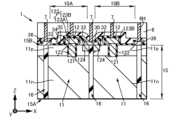
- 60 is a vertical cross-sectional configuration diagram (a cross-sectional view taken along line GG shown in FIG. 61) of a pixel of a solid-state imaging device according to a seventh embodiment of the present disclosure, corresponding to FIG. 2.
- FIG. 61 is a plan view of the pixel shown in FIG. 60, corresponding to FIG.
- FIG. 62 is a cross-sectional view illustrating a first step for explaining each step of a method for manufacturing a solid-state imaging device according to the eighth embodiment.
- FIG. 63 is a cross-sectional view of the second process.
- FIG. 64 is a cross-sectional view of the third step.
- FIG. 65 is a cross-sectional view of the fourth step.
- FIG. 66 is a cross-sectional view illustrating a first step for explaining each step of a method for manufacturing a solid-state imaging device according to the ninth embodiment.
- FIG. 67 is a cross-sectional view of the second process.
- FIG. 68 is a plan view of a pixel of a solid-state imaging device according to a tenth embodiment of the present disclosure, corresponding to FIG.
- FIG. 69 is a vertical cross-sectional configuration diagram (a cross-sectional view taken along the HH cutting line shown in FIG.
- FIG. 70 is a plan view of the pixel shown in FIG. 69
- FIG. 71 is a plan view illustrating the configuration of a pixel of a solid-state imaging device according to a twelfth embodiment of the present disclosure
- FIG. 72 is a block diagram showing an example of a schematic configuration of a vehicle control system, which is a first application example according to an embodiment of the present disclosure.
- FIG. 73 is an explanatory diagram showing an example of the installation positions of the outside-vehicle information detection unit and the imaging unit.
- First embodiment In the first embodiment, an example in which the present technology is applied to a solid-state imaging device will be described. In the first embodiment, the circuit configuration, planar configuration, longitudinal cross-sectional configuration, and manufacturing method of the solid-state imaging device will be described in detail. 2.
- Second Embodiment The second embodiment is a first example in which the isolation structure between the gate electrode of the transfer transistor of a pixel and the floating diffusion in the solid-state imaging device according to the first embodiment is changed. 3.
- Third Embodiment The third embodiment is a second example in which the structure of the pixel isolation region that isolates pixels in the solid-state imaging device according to the first embodiment is changed. 4.
- the fourth embodiment is a fourth example illustrating an isolation structure in other regions in addition to the isolation structure between the gate electrode of the transfer transistor of a pixel and the floating diffusion in the solid-state imaging device according to the first embodiment. 5.
- Fifth Embodiment is a fifth example in which the isolation structure between the gate electrode of the transfer transistor of a pixel and the floating diffusion in the solid-state imaging device according to the first embodiment is changed. 6.
- Sixth embodiment is a sixth example in which the structure of the shared connection portion of the floating diffusion is changed in the solid-state imaging device according to the first embodiment.
- a manufacturing method of the solid-state imaging device will also be described. 7.
- the seventh embodiment is a seventh example in which a transistor that constitutes a pixel circuit is provided in a pixel in the solid-state imaging device according to the first embodiment.
- the eighth embodiment is an eighth example in which the manufacturing method of the isolation structure between the gate electrode of the transfer transistor of a pixel and the floating diffusion in the solid-state imaging device according to the first embodiment is changed.
- the ninth embodiment is a ninth example in which the method of manufacturing the isolation structure between the gate electrode of the transfer transistor of a pixel and the floating diffusion in the solid-state imaging device according to the first embodiment is changed. 10.
- the tenth embodiment is a tenth example in which the structure of the pixel isolation region that isolates pixels in the solid-state imaging device according to the first embodiment is changed.
- the eleventh embodiment is an eleventh example in which the structure of the pixel isolation region that isolates pixels in the solid-state imaging device according to the first embodiment is changed.
- Twelfth Embodiment is a twelfth example in which the structure of the unit pixel is changed in the solid-state imaging device according to the first embodiment.
- Application Example to a Mobile Body An example in which the present technology is applied to a vehicle control system, which is an example of a mobile body control system, will be described. 14.
- a solid-state imaging device 1 according to a first embodiment of the present disclosure will be described with reference to FIGS.
- the arrow X direction shown as appropriate in the figure indicates one planar direction of the solid-state imaging device 1 placed on a flat surface for convenience.
- the arrow Y direction indicates another planar direction perpendicular to the arrow X direction.
- the arrow Z direction indicates an upward direction perpendicular to the arrow X and arrow Y directions.
- the arrow X direction, the arrow Y direction, and the arrow Z direction exactly coincide with the X-axis direction, the Y-axis direction, and the Z-axis direction, respectively, of a three-dimensional coordinate system. Note that these directions are shown to facilitate understanding of the description, and are not intended to limit the directions of the present technology.
- FIG. 1 shows an example of the circuit configuration of the pixel 10 and pixel circuit 20 that constitute the solid-state imaging device 1.
- Each pixel 10 is composed of a series circuit of a photoelectric conversion element (photodiode) 11 and a transistor 12.
- a photoelectric conversion element photodiode
- transistor 12 a transistor
- the photoelectric conversion element 11 converts light incident from outside the solid-state imaging device 1 into an electric charge (electrical signal).
- the transistor 12 is used as a transfer transistor that transfers the electric charge converted in the photoelectric conversion element 11 to the pixel circuit 20.
- the transistor 12 is an insulated gate field effect transistor (IGFET). More specifically, the transistor 12 is an n-channel conductivity type IGFET that is a first conductivity type. That is, the transistor 12 includes a gate electrode and a pair of main electrodes.
- the transistor 12 is the "first transistor” or the "second transistor” according to the present technology.
- the gate electrode is connected to a horizontal signal line (not shown).
- a control signal TG is input to the gate electrode from the horizontal signal line. The on/off operation of the transistor 12 is controlled by the control signal TG.
- the pixel circuit 20 is provided for each unit pixel. In the first embodiment, one pixel circuit 20 is provided for four pixels 10. The pixel circuit 20 performs signal processing of charges converted from light in the pixel 10.
- the pixel circuit 20 includes an amplification transistor 21 , a selection transistor 22 , a floating diffusion conversion gain switching transistor (hereinafter simply referred to as “FD conversion gain switching transistor”) 23 , and a reset transistor 24 .
- the gate electrode of the amplifier transistor 21 is connected to the FD 25.
- One main electrode of the amplifier transistor 21 is connected to the power supply voltage terminal VDD, and the other main electrode is connected to one main electrode of the selection transistor 22.
- the gate electrode of the selection transistor 22 is connected to a selection signal line SEL.
- the other main electrode of the selection transistor 22 is connected to a vertical signal line VSL and a current source load LC.
- the current source load LC is connected to a reference voltage terminal GND.
- a gate electrode of the FD conversion gain switching transistor 23 is connected to a floating diffusion control signal line FDG.
- One main electrode of the FD conversion gain switching transistor 23 is connected to the FD 25, and the other main electrode is connected to one main electrode of the reset transistor 24.
- the gate electrode of the reset transistor 24 is connected to a reset signal line RST.
- the other main electrode of the reset transistor 24 is connected to a power supply voltage terminal VDD.
- the pixel circuits 20 are further connected to an image processing circuit (not shown) that includes, for example, an analog-to-digital converter (ADC) and a digital signal processor (DSP).
- ADC analog-to-digital converter
- DSP digital signal processor
- the charge converted from light by the pixel 10 is an analog signal.
- This analog signal is amplified in the pixel circuit 20.
- the ADC converts the analog signal output from the pixel circuit 20 into a digital signal.
- the DSP performs functional processing of the digital signal.
- the image processing circuit performs signal processing for image creation.
- FIG. 3 shows an example of a schematic vertical cross-sectional structure of the pixel 10.
- Fig. 4 shows an example of a schematic planar structure of the pixel 10.
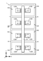
- the unit pixel is composed of four pixels 10 arranged adjacent to each other. More specifically, the unit pixel includes two pixels 10A and 10B arranged adjacent to each other in the direction of the arrow X, and two pixels 10C and 10D arranged adjacent to each other in the direction of the arrow Y and adjacent to each other in the direction of the arrow X. In other words, the pixels 10A to 10D are arranged in a matrix. When viewed from the direction of the arrow Z (hereinafter simply referred to as "in a plan view"), each of the pixels 10A to 10D is formed in a rectangular shape.
- the "pixel 10" is given a reference number that distinguishes it from the "pixels 10A" to the “pixels 10D.” Note that when referring to them collectively, they may be simply referred to as the "pixels 10.”
- the pixels 10 are disposed on a base 15.
- a semiconductor substrate is used for the base 15. More specifically, a single crystal silicon (Si) substrate having a p-type semiconductor region (or a p-type well region) of the second conductivity type is used.
- each of pixels 10A to 10D is further disposed within an area surrounded by pixel isolation regions 16.
- pixel isolation regions 16 are formed in a lattice pattern.
- the pixel isolation region 16 includes a groove 161, an embedding member 163, and an embedding member 164.
- the groove 161 is formed as a groove extending in the depth direction from the second surface 15B on the arrow Z direction side of the base 15 to the first surface 15A side opposite to the arrow Z direction.
- the first surface 15A is used as a light incidence surface of the pixel 10.
- the filling member 163 is on the first surface 15A side of the groove 161 and fills most of the inside of the groove 161.
- the filling member 163 is, for example, a polycrystalline silicon film.
- the filling member 164 is embedded in the groove 161 on the second surface 15B side of the groove 161 and on the filling member 163.
- the filling member 164 is, for example, a silicon oxide (SiO) film, a silicon nitride (SiN) film, or the like. That is, the pixel isolation region 16 has a trench isolation structure.
- the pixel isolation region 16 also includes a pinning region 162 formed in the base 15 in a region along the filling member 163 of the groove 161 .
- the photoelectric conversion element 11 of the pixel 10 is disposed on the first surface 15A side of the base 15.
- the photoelectric conversion element 11 is disposed for each of the pixels 10A to 10D. That is, one photoelectric conversion element 11 (corresponding to the "first photoelectric conversion element” according to the present technology) is disposed in the pixel 10A. Also, one photoelectric conversion element 11 (corresponding to the "second photoelectric conversion element” according to the present technology) is disposed in the pixel 10B. Similarly, one photoelectric conversion element 11 is disposed in the pixel 10C, and one photoelectric conversion element 11 is disposed in the pixel 10D.
- the photoelectric conversion element 11 is formed at the pn junction between the p-type semiconductor region 11p and the n-type semiconductor region 11n.
- the p-type semiconductor region 11p is disposed on the second surface 15B side of the base 15 within the region surrounded by the pixel isolation region 16.
- the n-type semiconductor region 11n is similarly disposed on the first surface 15A side of the base 15 within the region surrounded by the pixel isolation region 16.
- the transistor (transfer transistor) 12 of the pixel 10 includes an n-type semiconductor region 11 n as one main electrode, an n-type semiconductor region 124 as the other main electrode, a gate insulating film 122 , and a gate electrode 123 .
- the n-type semiconductor region 11 n is the n-type semiconductor region 11 n of the photoelectric conversion element 11 .
- the gate insulating film 122 is formed along the inner wall of the groove 121 that reaches the n-type semiconductor region 11n from the second surface 15B of the base 15.
- a single layer film of a SiO film or a SiN film, or a composite film of a combination of these films is used.
- the gate electrode 123 includes a vertical gate electrode portion 123 A and a gate electrode connection portion 123 B.
- the gate electrode 123 corresponds to a “first gate electrode” or a “second gate electrode” according to the present technology.
- the vertical gate electrode portion 123A is buried in the trench 121 with a gate insulating film 122 interposed therebetween.
- a polycrystalline Si film is used for the vertical gate electrode portion 123A. This polycrystalline Si film contains impurities that reduce the resistance value.
- the gate electrode connection portion 123B is disposed on the second surface 15B of the base body 15.
- the gate electrode connection portion 123B is in contact with and electrically connected to the vertical gate electrode portion 123A.
- the gate electrode connection portion 123B is also electrically connected to the wiring 7.
- a control signal TG is input from the wiring 7 to the gate electrode connection portion 123B.
- the gate electrode connection portion 123B is made of, for example, a polycrystalline Si film.
- the n-type semiconductor region 124 is disposed on the surface portion of the p-type semiconductor region 11p on the second surface 15B side of the base 15.
- the n-type semiconductor region 124 is disposed in a position close to the pixel isolation region 16.
- the n-type semiconductor regions 124 of the four pixels 10A to 10D that make up the unit pixel are gathered at the center position of the unit pixel.
- a shared contact 30 is electrically connected to the n-type semiconductor region 124 of the transistor 12.
- the shared contact 30 is configured as a common connection part for a total of four n-type semiconductor regions 124 of the four pixels 10A to 10D that constitute a unit pixel.
- the shared contact 30 is configured as a part of the FD 25 (see FIG. 1), and is electrically connected to the pixel circuit 20 (see FIG. 1) through the wiring 7.
- the shared connection portion 30 is disposed on the second surface 15B side of the base 15 so as to overlap the pixel isolation region 16. To explain in more detail, the shared connection portion 30 overlaps the pixel isolation region 16 and is extended from this overlapping position into each of the n-type semiconductor regions 124 of the pixels 10A to 10D so as to overlap with the n-type semiconductor regions 124. In this extended and overlapping region, the shared connection portion 30 is electrically connected to each of the four n-type semiconductor regions 124.
- the side surface of the shared connection portion 30 on the gate electrode 123 (gate electrode connection portion 123B) side is formed into a shape that approaches the gate electrode 123 as it moves away from the second surface 15B of the base body 15 (as it moves toward the direction of the arrow Z).
- the side surface of the shared connection portion 30 on the gate electrode 123 side is formed into an arc-shaped cross-sectional shape that protrudes toward the shared connection portion 30 side and rides onto the upper portion of the gate electrode 123.
- the side surface of the shared connection unit 30 on the gate electrode 123 (corresponding to the "first gate electrode” in the present technology) side of the pixel 10A is formed in a shape that approaches the gate electrode (first gate electrode) 123 as it is moved away from the second surface 15B.
- the side surface of the shared connection unit 30 on the gate electrode 123 (corresponding to the "second gate electrode” in the present technology) side of the pixel 10B is formed in a shape that approaches the gate electrode (second gate electrode) 123 as it is moved away from the second surface 15B.
- the shape of the side surface of the shared connection unit 30 is similar for each of the pixels 10C and 10D.
- the shared connection portion 30 is made of, for example, a polycrystalline silicon film. This polycrystalline silicon film contains impurities that reduce the resistance value.
- a low dielectric region 32 is disposed between the gate electrode 123 of the transistor 12 in the pixel 10 and the FD 25 (see FIG. 1).
- the low dielectric constant region 32 is disposed between the gate electrode connection portion 123B of the gate electrode 123 and the shared connection portion 30 as a part of the FD 25.
- the low dielectric constant region 32 is on the opposite side of the gate electrode connection portion 123B from the shared connection portion 30, and has a lower dielectric constant than a non-facing region 33 surrounded by a dashed line.
- the non-facing region 33 includes an insulating film 34 that covers a part of the side surface of the gate electrode connection portion 123B, and an insulating film 35 that is laminated and covers the insulating film 34.
- the insulating film 34 is formed of, for example, a SiO film.
- the insulating film 35 is formed of, for example, a SiN film.
- the low dielectric constant region 32 is a gap.
- the low dielectric constant region 32 is a gap containing gas therein. Air is used as the gas.
- the low dielectric constant region 32 is configured as an air gap here.
- the capacitance value of the parasitic capacitance with the gate electrode connection portion 123B as one electrode, the low dielectric constant region 32 as the dielectric, and the shared connection portion 30 as the other electrode is reduced.
- the capacitance value of the parasitic capacitance generated in each of the pixels 10A to 10D is reduced, and as a result, it is possible to effectively suppress or prevent variation in the capacitance value of the parasitic capacitance added to the FD 25.
- the gap serving as the low dielectric constant region 32 may be a vacuum.
- the gap serving as the low dielectric constant region 32 may be filled with an inert gas such as nitrogen gas (N 2 ) or argon gas (Ar).
- the wiring 7 is disposed in a connection hole 6H formed in the insulating film 34, the insulating film 35, and the interlayer insulating film 6, which respectively cover the transistor 12 and the shared connection portion 30.
- the connection hole 6H is a through hole formed in the thickness direction of the insulating film 34, the insulating film 35, and the interlayer insulating film 6.
- the interlayer insulating film 6 is formed of, for example, a SiO film.
- the wiring 7 is formed of, for example, a tungsten (W) film. That is, the wiring 7 is formed as a so-called W plug.
- the solid-state imaging device 1 employs a two-stage structure in which the base 15 including the photoelectric conversion elements 11 and the transistors (transfer transistors) 12 is stacked on the substrate 15 and a substrate on which the pixel circuits 20 are constructed.
- Method of manufacturing the solid-state imaging device 1] 4 to 25 show an example of a manufacturing method for the solid-state imaging device 1 according to the first embodiment, step by step.
- illustrations and descriptions of the respective structures of the photoelectric conversion element 11 and the transistor (transfer transistor) 12 are simplified or omitted.
- a substrate 15 is prepared.
- the substrate 15 is, for example, a single crystal Si substrate.
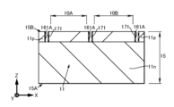
- a groove 161A is formed from the surface of the second face 15B of the base 15 toward the first face 15A.
- This groove 161A has a shallower depth than the groove 161 to be formed later.
- the groove 161A has a depth that reaches the n-type semiconductor region 11n of the photoelectric conversion element 11.
- the groove 161A is formed by using, for example, photolithography technology and etching technology. For the etching, anisotropic etching such as reactive ion etching (RIE) is used. 5, a mask 171 is formed along the inner wall of the groove 161A.
- the mask 171 is used as an etching mask and an impurity introduction mask.
- the mask 171 is a composite film formed by sequentially laminating, for example, a SiO film and a SiN film.
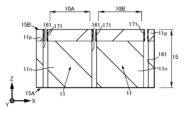
- the mask 171 is used to further deepen the groove 161A, forming the groove 161.
- anisotropic etching is used to form the groove 161.
- pinning regions 162 are formed in the surface portion of the base 15 along the inner wall of the groove 161, specifically, in the surface portion of the n-type semiconductor region 11n (see FIG. 3).
- the pinning regions 162 are formed by introducing p-type impurities into the n-type semiconductor region 11n using a mask 171. As shown in FIG. 8, mask 171 is removed.
- a filling material 163 is formed on the entire surface of the second surface 15B of the base body 15.
- the filling material 163 is, for example, a polycrystalline Si film formed by chemical vapor deposition (CVD). Subsequently, the entire surface of the base 15 is etched to remove excess filling material 163 on the second surface 15B, thereby filling the grooves 161 with filling material 163, as shown in FIG.
- a filling member 164 is further embedded on the filling member 163 in the groove 161.
- the filling member 164 is, for example, a SiO film formed by CVD. As with the filling member 163, excess filling member 164 is removed by etching after the film formation. When this process is completed, the pixel isolation region 16 is completed.
- An insulating film 341 is formed on the second surface 15B of the base 15 (see FIG. 12).
- This insulating film 341 is used as a gate insulating film of the transistor 12.
- the gate electrode connection portion 123B is formed on the insulating film 341.
- the vertical gate electrode portion 123A (see FIG. 2) of the transistor 12 is already formed, and the gate electrode connection portion 123B is formed on the vertical gate electrode portion 123A and electrically connected thereto.
- a polycrystalline Si film formed by CVD is used for the gate electrode connection portion 123B.
- an insulating film 342 is formed to cover the side and upper surfaces of the gate electrode connection portion 123B.
- the insulating film 342 is, for example, a SiO film formed by using a CVD method.
- an insulating film 351 is formed on the side and upper surfaces of the gate electrode connection portion 123B with the insulating film 342 therebetween.
- the insulating film 351 is, for example, a SiN film formed by CVD.
- etching is performed on the entire surface, leaving insulating film 351 on the side of gate electrode connection portion 123B, and removing insulating film 351 in other areas.
- Anisotropic etching such as RIE is used for the etching.
- the insulating film 351 left on the side of gate electrode connection portion 123B is used as a so-called sidewall spacer.
- an insulating film 343 is formed on the upper surface of the gate electrode connection portion 123B and on the upper surface of the insulating film 351.
- the insulating film 343 is, for example, a SiO film formed by using a CVD method.
- the insulating film 343 is used as a buffer film, and an n-type semiconductor region 124 to be used as the other main electrode of the transistor 12 is formed in a surface portion of the second face 15B of the base 15.
- the n-type semiconductor region 124 is formed by introducing an n-type impurity into the base 15 by using, for example, an ion implantation method. Once the n-type semiconductor region 124 is formed, the transistor 12 is complete.
- an opening 343H is formed in the insulating film 343 in a region overlapping the n-type semiconductor region 124 and the pixel isolation region 16.
- the opening 343H is formed using photolithography and etching techniques.
- a conductive film 301 is formed on the entire surface of the base 15 including the insulating film 343.
- the conductive film 301 is a material that forms the shared connection portion 30.
- a polycrystalline Si film formed by using, for example, a CVD method is used for the conductive film 301.
- a p-type impurity is introduced into the conductive film 301 to form a p-type conductive film 36.
- This p-type conductive film 36 is used as a path for supplying a reference voltage, for example. 20, n-type impurities are introduced into the conductive film 301 in the region for forming the shared connection portion 30. When the n-type impurities are introduced, the shared connection portion 30 is substantially formed.
- the conductive film 301 is patterned and excess conductive film 301 is removed to form the shared connection portion 30 and the p-type conductive film 36. Photolithography and etching techniques are used for the patterning.
- the insulating film 343 and the insulating film 351 are selectively removed.
- An etching technique is used for this selective removal.
- the insulating film 351 is formed as a sidewall spacer, and is removed to form the low dielectric constant region 32 that serves as a gap between the gate electrode connection portion 123B and the shared connection portion 30. That is, the low dielectric constant region 32 is formed by forming a sidewall spacer on the side surface of the gate electrode connection portion 123B and utilizing the gap created by removing this sidewall spacer.
- the gap, which is the low dielectric constant region 32 will be filled with air. Also, if a vacuum is drawn in the furnace during the manufacturing process, the gap, which is the low dielectric constant region 32, will become a vacuum. Furthermore, if a carrier gas, such as an inert gas, is used to flow in the furnace during the manufacturing process, the gap, which is the low dielectric constant region 32, will be filled with the inert gas.
- a carrier gas such as an inert gas
- an insulating film 34 is formed on the entire second surface 15B of the base 15 to cover the shared connection portion 30. Furthermore, an insulating film 35 is formed on the insulating film 34 as shown in FIG.
- a non-facing region 33 including the insulating film 34 and the insulating film 35 is formed in a region other than the region in which the low dielectric constant region 32 is formed.
- the dielectric constant of the low dielectric constant region 32 is smaller than the dielectric constant of the non-facing region 33.
- the interlayer insulating film 6 is formed on the insulating film 35 . Subsequently, a contact hole 6H is formed in the interlayer insulating film 6, and as shown in FIG. 2, a wiring 7 is formed in the contact hole 6H. It should be noted that the illustration and description of the manufacturing method for the pixel circuit 20 (see FIG. 1) and the like will be omitted.
- the solid-state imaging device 1 according to the first embodiment is completed and the manufacturing method is completed.
- the solid-state imaging device 1 includes a pixel (first pixel) 10, a transistor (first transistor) 12, and an FD 25.
- the pixel 10 is, for example, pixel 10A.
- the pixel 10 is disposed on the first surface 15A side of the base 15, which is the light incident side, and has a photoelectric conversion element (first photoelectric conversion element) 11 that converts light into electric charges.
- the transistor 12 is disposed on the second surface 15B side of the base 15 opposite to the first surface 15A at a position corresponding to the pixel 10.
- the transistor 12 has a gate electrode (first gate electrode) 123, and one of a pair of main electrodes is electrically connected to the photoelectric conversion element 11.
- the FD 25 is disposed on the second surface 15B side of the base 15, and is electrically connected to an n-type semiconductor region 124 that is the other main electrode of the transistor 12. 2 and 3, the solid-state imaging device 1 further includes a low dielectric constant region 32.
- the low dielectric constant region 32 is disposed between the FD 25 and the gate electrode 123 facing the FD 25.
- the low dielectric constant region 32 has a lower dielectric constant than a non-facing region 33 that does not face the FD 25.
- the solid-state imaging device 1 further includes a pixel (second pixel) 10 and a transistor (second transistor) 12.
- the pixel 10 is, for example, pixel 10B (or pixel 10C).
- the pixel 10 is disposed adjacent to the pixel 10A as the first pixel, for example.
- the pixel 10 is disposed on the first surface 15A side of the base 15, and has a photoelectric conversion element (second photoelectric conversion element) 11 that converts light into electric charges.
- the transistor 12 is disposed on the second surface 15B side of the base 15 at a position corresponding to the pixel 10.
- the transistor 12 has a gate electrode (second gate electrode) 123, one of a pair of main electrodes is electrically connected to the photoelectric conversion element 11, and the FD 25 is electrically connected to the n-type semiconductor region 124, which is the other main electrode.
- the solid-state imaging device 1 further includes a low dielectric constant region 32 between the FD 25 and the gate electrode 123 facing the FD 25 . With this configuration, it is possible to reduce the capacitance value of the parasitic capacitance in which the gate electrode 123 is one electrode, the low dielectric constant region 32 is the dielectric, and the FD 25 is the other electrode.
- the solid-state imaging device 1 further includes a pixel isolation region 16 and a shared connection portion 30 .
- the pixel isolation region 16 is disposed in the base 15 between two adjacent pixels (first pixel) 10 and (second pixel) 10, and electrically and optically isolates the pixels 10.
- the pixel isolation region 16 includes a groove 161 formed in the depth direction of the base 15, and an embedding member 163 and an embedding member 164 embedded in the groove 161.
- the shared connection portion 30 is disposed on the second surface 15B side of the base 15 so as to overlap the pixel isolation region 16, and electrically connects, for example, the other main electrodes (n-type semiconductor regions 124) of the transistor (first transistor) 12 of the pixel 10A and the transistor (second transistor) 12 of the pixel 10B.
- the FD 25 is electrically connected to the shared connection portion 30.
- a low dielectric constant region 32 is disposed between the gate electrode 123 and the shared connection portion 30 . Therefore, the capacitance value of the parasitic capacitance between the gate electrode 123 and the shared connection portion 30 can be reduced.
- the side of the shared connection portion 30 facing the gate electrode (first gate electrode and second gate electrode) 123 is formed in a shape that approaches the gate electrode 123 as it moves away from the second surface 15B of the base 15 in the direction of the arrow Z. 21 of the manufacturing method, the shared connection portion 30 is formed on the side surface of the gate electrode 123 (specifically, the gate electrode connection portion 123B) in a shape that encloses the insulating film 351 serving as a sidewall spacer.
- the low dielectric constant region 32 is formed by utilizing the gap created by selectively removing the insulating film 351. Therefore, the low dielectric constant region 32 can be easily formed, and the capacitance value of the parasitic capacitance can be easily reduced.
- the low dielectric constant region 32 is a gap.
- the gap of the low dielectric constant region 32 is a vacuum.
- the gap of the low dielectric constant region 32 is filled with air or an inert gas. Therefore, the low dielectric constant region 32 can be simply configured, and the capacitance value of the parasitic capacitance can be easily reduced.
- Second embodiment> A solid-state imaging device 1 according to a second embodiment of the present disclosure will be described with reference to Figures 26 and 27. Note that in the second embodiment and the following embodiments, components that are the same as or substantially the same as components of the solid-state imaging device 1 according to the first embodiment are denoted by the same reference numerals, and duplicated descriptions will be omitted.
- FIG. 26 shows an example of a schematic vertical cross-sectional structure of the pixel 10.
- Fig. 27 shows an example of a schematic planar structure of the pixel 10.
- the low dielectric constant region 32 of the solid-state imaging device 1 according to the first embodiment is formed from a low dielectric constant material.
- the low dielectric constant material has a lower dielectric constant than the non-facing region 33.
- the insulating film 34 is a SiO film
- the insulating film 35 is a SiN film to form the non-facing region 33. Therefore, the low dielectric constant region 32 is formed of a single layer film of a SiO film or a carbon-added silicon oxide (SiOC) film, or a composite film formed by laminating these.
- the components other than those described above are the same or substantially the same as the components of the solid-state imaging device 1 according to the first embodiment.
- Fig. 28 shows an example of a schematic vertical cross-sectional structure of the pixel 10.
- Fig. 29 shows an example of a schematic planar structure of the pixel 10.
- the solid-state imaging device 1 according to the third embodiment has a different configuration of the pixel isolation region 16 from the solid-state imaging device 1 according to the first or second embodiment.
- the pixel isolation region 16 is configured with an insulator region instead of the structure including the groove 161, the filling member 163, and the filling member 164.
- the insulator region is formed by injecting impurities into the base 15 using, for example, an ion implantation method.
- the components other than those described above are the same or substantially the same as the components of the solid-state imaging device 1 according to the first or second embodiment.
- the pixel isolation region 16 is formed from an insulating region. Therefore, the pixel isolation region 16 can be easily formed, and the structure of the solid-state imaging device 1 can be easily realized.
- Fig. 30 shows an example of a schematic vertical cross-sectional structure of the pixel 10.
- Fig. 31 shows an example of a schematic planar structure of the pixel 10.
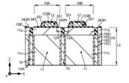
- the solid-state imaging device 1 according to the fourth embodiment is formed in a state where an insulating film 351 is left in the non-facing region 33 in the solid-state imaging device 1 according to the first or second embodiment.
- the insulating film 351 is a sidewall spacer formed on a side surface of the gate electrode connection portion 123B of the transistor 12.
- the components other than those described above are the same or substantially the same as the components of the solid-state imaging device 1 according to the first or second embodiment.
- the solid-state imaging device 1 according to the fourth embodiment may be applied to the solid-state imaging device 1 according to the third embodiment.
- an insulating film 351 is disposed as a sidewall spacer on the side surface of the non-facing region 33 of the gate electrode 123 (gate electrode connection portion 123B).
- the capacitance value of the parasitic capacitance added to the FD 25 is small, so that the signal variation and delay caused by the parasitic capacitance can be improved.
- FIG. 32 shows an example of a schematic vertical cross-sectional structure of the pixel 10.
- Fig. 33 shows an example of a schematic planar structure of the pixel 10.
- an insulating film 35 is formed on the gate electrode connection portion 123B of the transistor 12 and on the shared connection portion 30.
- the insulating film 34 is omitted (see FIG. 2).
- the insulating film 35 is made of, for example, a SiN film, which has poorer embedding ability than, for example, a SiO film.
- the components other than those described above are the same or substantially the same as the components of the solid-state imaging device 1 according to the first or second embodiment.
- the solid-state imaging device 1 according to the fifth embodiment may be applied to the solid-state imaging device 1 according to the third or fourth embodiment.
- Fig. 34 shows an example of a schematic vertical cross-sectional structure of the pixel 10.
- Fig. 35 shows an example of a schematic planar structure of the pixel 10.
- a portion of the shared connection portion 30 is embedded in a groove 161 of the pixel isolation region 16. More specifically, a portion of the shared connection portion 30 is embedded in the upper portion of the groove 161, and is further electrically connected to a side surface of the n-type semiconductor region 124 of the transistor 12 of the adjacent pixel 10. It is sufficient that the portion of the shared connection portion 30 is embedded to approximately the junction depth of the n-type semiconductor region 124.
- Method of manufacturing the solid-state imaging device 1 36 to 59 show an example of a manufacturing method for the solid-state imaging device 1 according to the sixth embodiment, step by step.
- illustrations and descriptions of the cross-sectional structures of the photoelectric conversion elements 11 and the transistors (transfer transistors) 12 are simplified or omitted.
- a base 15 is prepared. 36, a mask 172 and a mask 173 are sequentially formed on the second surface 15B of the base 15.
- the mask 172 is used as an etching stopper, for example, and is formed of a SiN film.
- the mask 173 is used as a hard mask for etching, for example, and is formed of a SiO film.
- an opening 173H is formed in the mask 173 in the region where the pixel isolation region 16 is to be formed.
- the opening 173H is formed by using, for example, photolithography and etching techniques.
- a groove 161A is formed from the surface of the second face 15B of the base 15 toward the first face 15A using a mask 173.
- the groove 161A has a shallow depth.
- the groove 161A is formed by using, for example, an etching technique.
- a mask 171 is formed along the inner wall of the groove 161A, as shown in FIG.
- the mask 171 is used to further deepen the groove 161A, forming the groove 161, as shown in FIG.
- pinning regions 162 are formed in the surface portions of the base 15 along the inner walls of the grooves 161, as shown in FIG. Thereafter, as shown in FIG. 42, the mask 171 is removed.
- an embedding member 163 is formed on the entire second surface 15B of the base 15.
- the embedding member 163 is formed on a mask 173.
- the entire surface of the base 15 is etched to remove excess filling material 163 on the mask 173.
- the filling material 163 is filled into the grooves 161, as shown in FIG.
- a filling material 164 is further filled in the groove 161 on the filling material 163.
- the excess filling material 164 on the mask 173 is removed.
- the mask 173 and the filling material 164 remaining in the opening 173H are removed by etching.
- a portion of the embedding member 164 is further removed using the mask 172.
- a conductive film 301 is formed on the entire surface of the substrate 15, including on the mask 172.
- the conductive film 301 is a material that forms the shared connection portion 30.
- a portion of the conductive film 301 is embedded in the upper portion of the groove 161 of the pixel isolation region 16.
- a p-type impurity is introduced into the conductive film 301 in the portion overlapping the pixel isolation region 16 except for the region where the shared connection portion 30 is formed, and a p-type conductive film 36 is formed.
- n-type impurities are introduced into the conductive film 301 in the region for forming the shared connection portion 30.
- the shared connection portion 30 is substantially formed.
- the conductive film 301 is patterned and excess conductive film 301 is removed to form the shared connection portion 30 and the p-type conductive film 36. Subsequently, mask 172 is removed, as shown in FIG.
- an insulating film 341 is formed on the second surface 15B of the base 15 in the region where the pixel 10 is formed.
- the n-type semiconductor region 124 of the transistor 12 is formed (see FIG. 53).
- the n-type semiconductor region 124 is formed by introducing an n-type impurity into the surface portion of the second face 15B of the base body 15 through the insulating film 341.
- a side surface of the n-type semiconductor region 124 contacts a side surface of the shared connecting portion 30, and the two are electrically connected to each other.
- a gate electrode connection portion 123B of the gate electrode 123 is formed on the insulating film 341 as shown in FIG. 14 of the first manufacturing method, an insulating film 342 and an insulating film 351 are sequentially formed on the entire surface of the second surface 15B side of the base 15 as shown in FIG.
- etching is performed on the entire surface, so that the insulating film 351 is left on the side surface of the gate electrode connection portion 123B and the insulating film 351 is removed from other regions as shown in Fig. 55.
- the remaining insulating film 351 is formed as a sidewall spacer.
- an insulating film 344 is formed to cover the gate electrode connection portion 123B and the insulating film 351.
- the insulating film 344 is, for example, a SiO film.
- the insulating film 344, the insulating film 351, etc. are removed. This removal exposes the surfaces of the gate electrode connection portion 123B, the shared connection portion 30, etc.
- an insulating film 34 is formed to cover the gate electrode connection portion 123B, the shared connection portion 30, etc.
- the insulating film 34 is, for example, a SiO film, as in the first manufacturing method.
- a gap is generated between the gate electrode connection portion 123B and the shared connection portion 30, and as a result, a low dielectric constant region 32 is formed.
- the thickness of the shared connection part 30 in the direction of the arrow Z is set to be large, the height of the low dielectric constant region 32 in the same direction becomes large. In other words, the volume of the low dielectric constant region 32 can be increased, and the capacitance value of the parasitic capacitance can be reduced.
- an insulating film 35 is formed on the insulating film 34 .
- the components other than those mentioned above are the same or substantially the same as the components of the solid-state imaging device 1 according to the first or second embodiment.
- the solid-state imaging device 1 according to the sixth embodiment may be applied to any of the solid-state imaging devices 1 according to the third to fifth embodiments.
- Fig. 60 shows an example of a schematic vertical cross-sectional structure of the pixel 10.
- Fig. 61 shows an example of a schematic planar structure of the pixel 10.
- the solid-state imaging device 1 employs a one-stage structure in which a pixel circuit 20 is constructed on a base 15.
- transistors that construct the pixel circuit 20 are disposed on the second surface 15B of the base 15 at positions corresponding to the pixels 10.
- an amplification transistor 21 is disposed on the base 15 at a position corresponding to pixel 10A that constitutes a unit pixel. Furthermore, a selection transistor 22 is disposed on the base 15 at a position corresponding to pixel 10B. Similarly, an FD conversion gain switching transistor 23 is disposed on the base 15 at a position corresponding to pixel 10C, and a reset transistor 24 is disposed on the base 15 at a position corresponding to pixel 10D.
- An element isolation region 8 is disposed around each of the amplifying transistor 21, the selection transistor 22, the FD conversion gain switching transistor 23, and the reset transistor 24.
- the element isolation region 8 is configured with a trench isolation structure that includes a groove and a filling material filled in the groove, although a detailed structural description is omitted and no particular reference numeral is given to the region.
- each of the amplifying transistor 21, the selection transistor 22, the FD conversion gain switching transistor 23, and the reset transistor 24 has a gate electrode and a pair of main electrodes, although detailed structural explanations are omitted and no particular reference numerals are given to each.
- the gate electrode is formed in the same conductive layer and made of the same conductive material as the gate electrode connection portion 123B of the transistor 12.
- the pair of main electrodes is formed of the same n-type semiconductor region as the n-type semiconductor region 124 of the transistor 12.
- an insulating film 351 used as a sidewall spacer is disposed on the side of each gate electrode of the amplification transistor 21, the selection transistor 22, the FD conversion gain switching transistor 23, and the reset transistor 24.
- the present technology is not limited to arranging one transistor constituting the pixel circuit 20 at a position corresponding to one pixel 10.
- one transistor may be arranged across two pixels 10.
- two transistors may be arranged at positions corresponding to one pixel 10.
- the components other than those mentioned above are the same or substantially the same as the components of the solid-state imaging device 1 according to the first or second embodiment.
- the solid-state imaging device 1 according to the seventh embodiment may be applied to any of the solid-state imaging devices 1 according to the third to sixth embodiments.
- Method of manufacturing the solid-state imaging device 1] 62 to 65 show an example of a manufacturing method for the solid-state imaging device 1 according to the eighth embodiment, step by step.
- illustrations and descriptions of the cross-sectional structures of the photoelectric conversion elements 11 and the transistors (transfer transistors) 12 are simplified or omitted.
- an insulating film 351 used as a sidewall spacer is formed on the side surface of the gate electrode connection portion 123B, and an insulating film 343 covering the gate electrode connection portion 123B and the insulating film 351 is formed (see FIG. 62).
- an n-type semiconductor region 124 is formed as the other main electrode of the transistor 12 .
- the shared connecting portion 30 and the p-type conductive film 36 are formed as shown in FIG.
- the components other than those described above are the same or substantially the same as the components of the solid-state imaging device 1 and the manufacturing method thereof according to the first embodiment.
- Method of manufacturing the solid-state imaging device 1 66 and 67 show an example of a manufacturing method for the solid-state imaging device 1 according to the ninth embodiment, step by step.
- illustrations and descriptions of the cross-sectional structures of the photoelectric conversion elements 11 and the transistors (transfer transistors) 12 are simplified or omitted.
- the shared connection portion 30 and the p-type conductive film 36 are formed as shown in FIG. 66, similar to the process shown in FIG. 64 in the method for manufacturing the solid-state imaging device 1 according to the eighth embodiment (hereinafter simply referred to as the "eighth manufacturing method").
- a part of the shared connection portion 30 is embedded in the groove 161 of the pixel isolation region 16, similar to the process shown in FIGS. 47 to 53 in the method for manufacturing the solid-state imaging device 1 according to the sixth embodiment described above.
- the insulating film 34 and the insulating film 35 are formed in sequence.
- a low dielectric constant region 32 is formed between the gate electrode connection portion 123B and the shared connection portion 30.
- the components other than those described above are the same or substantially the same as the components of the solid-state imaging device 1 and the manufacturing method thereof according to the eighth embodiment.
- FIG. 68 shows an example of a schematic planar structure of a pixel 10.
- a pixel isolation region 16 is disposed in part of the periphery of a pixel 10 .
- a separation portion 16I is provided between pixels 10A and 10B constituting a unit pixel, where the pixel separation region 16 ends.
- a separation portion 16I is provided between pixels 10C and 10D, where the pixel separation region 16 ends.
- the components other than those described above are the same or substantially the same as the components of the solid-state imaging device 1 according to any one of the first to ninth embodiments.
- Fig. 69 shows an example of a schematic vertical cross-sectional structure of the pixel 10.
- Fig. 70 shows an example of a schematic planar structure of the pixel 10.
- the pixel isolation region 16 is composed of two types of pixel isolation region 16T and pixel isolation region 16R.
- the pixel isolation region 16T is the same component as the pixel isolation region 16 of the solid-state imaging device 1 according to the first or second embodiment. To distinguish between them, the reference numerals are changed.
- the pixel isolation region 16T is configured with a groove 161, an embedding member 163, and an embedding member 164.
- the pixel isolation region 16T is disposed around the unit pixel, between pixel 10A and pixel 10C, and between pixel 10B and pixel 10D.
- the pixel isolation region 16R is the same component as the pixel isolation region 16 of the solid-state imaging device 1 according to the third embodiment. Similarly, the reference numerals are changed to distinguish them.
- the pixel isolation region 16R is made of an insulating region.
- the pixel isolation region 16R is disposed between pixel 10A and pixel 10B, and between pixel 10C and pixel 10D.
- the components other than those described above are the same or substantially the same as the components of the solid-state imaging device 1 according to any one of the first to tenth embodiments.
- Twelfth embodiment A solid-state imaging device 1 according to a twelfth embodiment of the present disclosure will be described with reference to FIG.
- FIG. 71 shows an example of a schematic planar structure of a pixel 10.
- a unit pixel is constructed by a total of eight pixels 10A to 10H.
- Pixel 10B is arranged adjacent to pixel 10A in the direction of the arrow X.
- Pixel 10C is arranged adjacent to pixel 10A in the direction of the arrow Y.
- Pixel 10D is arranged adjacent to pixel 10C in the direction of the arrow X.
- Pixel 10E is arranged adjacent to pixel 10C in the direction of the arrow Y.
- Pixel 10F is arranged adjacent to pixel 10E in the direction of the arrow X.
- Pixel 10G is arranged adjacent to pixel 10F in the direction of the arrow Y.
- Pixel 10H is arranged adjacent to pixel 10G in the direction of the arrow X.
- the shared connection portion 30 is disposed extending between pixel 10A and pixel 10B, between pixel 10C and pixel 10D, between pixel 10E and pixel 10F, and between pixel 10G and pixel 10H.
- the shared connection portion 30 is shared by all pixels 10A to 10H of the unit pixel.
- one pixel circuit 20 (see FIG. 1) is provided for one unit pixel.
- the components other than those described above are the same or substantially the same as the components of the solid-state imaging device 1 according to any one of the first to eleventh embodiments.
- the technology according to the present disclosure can be applied to various products.
- the technology according to the present disclosure may be realized as a device mounted on any type of moving body such as an automobile, an electric vehicle, a hybrid electric vehicle, a motorcycle, a bicycle, a personal mobility device, an airplane, a drone, a ship, or a robot.
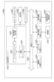
- FIG. 72 is a block diagram showing a schematic configuration example of a vehicle control system, which is an example of a mobile object control system to which the technology disclosed herein can be applied.
- the vehicle control system 12000 includes a plurality of electronic control units connected via a communication network 12001.
- the vehicle control system 12000 includes a drive system control unit 12010, a body system control unit 12020, an outside vehicle information detection unit 12030, an inside vehicle information detection unit 12040, and an integrated control unit 12050.
- Also shown as functional components of the integrated control unit 12050 are a microcomputer 12051, an audio/video output unit 12052, and an in-vehicle network I/F (Interface) 12053.
- the drive system control unit 12010 controls the operation of devices related to the drive system of the vehicle according to various programs.
- the drive system control unit 12010 functions as a control device for a drive force generating device for generating the drive force of the vehicle, such as an internal combustion engine or a drive motor, a drive force transmission mechanism for transmitting the drive force to the wheels, a steering mechanism for adjusting the steering angle of the vehicle, and a braking device for generating a braking force for the vehicle.
- the body system control unit 12020 controls the operation of various devices installed in the vehicle body according to various programs.
- the body system control unit 12020 functions as a control device for a keyless entry system, a smart key system, a power window device, or various lamps such as headlamps, tail lamps, brake lamps, turn signals, and fog lamps.
- radio waves or signals from various switches transmitted from a portable device that replaces a key can be input to the body system control unit 12020.
- the body system control unit 12020 accepts the input of these radio waves or signals and controls the vehicle's door lock device, power window device, lamps, etc.
- the outside-vehicle information detection unit 12030 detects information outside the vehicle equipped with the vehicle control system 12000.
- the image capturing unit 12031 is connected to the outside-vehicle information detection unit 12030.
- the outside-vehicle information detection unit 12030 causes the image capturing unit 12031 to capture images outside the vehicle and receives the captured images.
- the outside-vehicle information detection unit 12030 may perform object detection processing or distance detection processing for people, cars, obstacles, signs, or characters on the road surface based on the received images.
- the imaging unit 12031 is an optical sensor that receives light and outputs an electrical signal according to the amount of light received.
- the imaging unit 12031 can output the electrical signal as an image, or as distance measurement information.
- the light received by the imaging unit 12031 may be visible light, or may be invisible light such as infrared light.
- the in-vehicle information detection unit 12040 detects information inside the vehicle.
- a driver state detection unit 12041 that detects the state of the driver is connected.
- the driver state detection unit 12041 includes, for example, a camera that captures an image of the driver, and the in-vehicle information detection unit 12040 may calculate the driver's degree of fatigue or concentration based on the detection information input from the driver state detection unit 12041, or may determine whether the driver is dozing off.
- the microcomputer 12051 can calculate control target values for the driving force generating device, steering mechanism, or braking device based on information inside and outside the vehicle acquired by the outside vehicle information detection unit 12030 or the inside vehicle information detection unit 12040, and output control commands to the drive system control unit 12010.
- the microcomputer 12051 can perform cooperative control aimed at realizing the functions of an Advanced Driver Assistance System (ADAS), including vehicle collision avoidance or impact mitigation, following driving based on the distance between vehicles, maintaining vehicle speed, vehicle collision warning, or vehicle lane departure warning.
- ADAS Advanced Driver Assistance System
- the microcomputer 12051 can also control the driving force generating device, steering mechanism, braking device, etc. based on information about the surroundings of the vehicle acquired by the outside vehicle information detection unit 12030 or the inside vehicle information detection unit 12040, thereby performing cooperative control aimed at automatic driving, which allows the vehicle to travel autonomously without relying on the driver's operation.
- the microcomputer 12051 can also output control commands to the body system control unit 12030 based on information outside the vehicle acquired by the outside information detection unit 12030. For example, the microcomputer 12051 can control the headlamps according to the position of a preceding vehicle or an oncoming vehicle detected by the outside information detection unit 12030, and perform cooperative control aimed at preventing glare, such as switching high beams to low beams.
- the audio/image output unit 12052 transmits at least one output signal of audio and image to an output device capable of visually or audibly notifying the occupants of the vehicle or the outside of the vehicle of information.
- an audio speaker 12061, a display unit 12062, and an instrument panel 12063 are exemplified as output devices.
- the display unit 12062 may include, for example, at least one of an on-board display and a head-up display.
- FIG. 73 shows an example of the installation position of the imaging unit 12031.
- the imaging unit 12031 includes imaging units 12101, 12102, 12103, 12104, and 12105.
- the imaging units 12101, 12102, 12103, 12104, and 12105 are provided, for example, at the front nose, side mirrors, rear bumper, back door, and upper part of the windshield inside the vehicle cabin of the vehicle 12100.
- the imaging unit 12101 provided at the front nose and the imaging unit 12105 provided at the upper part of the windshield inside the vehicle cabin mainly acquire images of the front of the vehicle 12100.
- the imaging units 12102 and 12103 provided at the side mirrors mainly acquire images of the sides of the vehicle 12100.
- the imaging unit 12104 provided at the rear bumper or back door mainly acquires images of the rear of the vehicle 12100.
- the imaging unit 12105 provided at the upper part of the windshield inside the vehicle cabin is mainly used to detect leading vehicles, pedestrians, obstacles, traffic lights, traffic signs, lanes, etc.
- FIG. 73 shows an example of the imaging ranges of the imaging units 12101 to 12104.
- Imaging range 12111 indicates the imaging range of the imaging unit 12101 provided on the front nose
- imaging ranges 12112 and 12113 indicate the imaging ranges of the imaging units 12102 and 12103 provided on the side mirrors, respectively
- imaging range 12114 indicates the imaging range of the imaging unit 12104 provided on the rear bumper or back door.
- an overhead image of the vehicle 12100 viewed from above is obtained by superimposing the image data captured by the imaging units 12101 to 12104.
- At least one of the imaging units 12101 to 12104 may have a function of acquiring distance information.
- at least one of the imaging units 12101 to 12104 may be a stereo camera consisting of multiple imaging elements, or an imaging element having pixels for detecting phase differences.
- the microcomputer 12051 can obtain the distance to each solid object within the imaging ranges 12111 to 12114 and the change in this distance over time (relative speed with respect to the vehicle 12100) based on the distance information obtained from the imaging units 12101 to 12104, and can extract as a preceding vehicle, in particular, the closest solid object on the path of the vehicle 12100 that is traveling in approximately the same direction as the vehicle 12100 at a predetermined speed (e.g., 0 km/h or faster). Furthermore, the microcomputer 12051 can set the inter-vehicle distance that should be maintained in advance in front of the preceding vehicle, and perform automatic braking control (including follow-up stop control) and automatic acceleration control (including follow-up start control). In this way, cooperative control can be performed for the purpose of automatic driving, which runs autonomously without relying on the driver's operation.
- automatic braking control including follow-up stop control
- automatic acceleration control including follow-up start control
- the microcomputer 12051 classifies and extracts three-dimensional object data on three-dimensional objects, such as two-wheeled vehicles, ordinary vehicles, large vehicles, pedestrians, utility poles, and other three-dimensional objects, based on the distance information obtained from the imaging units 12101 to 12104, and can use the data to automatically avoid obstacles.
- the microcomputer 12051 distinguishes obstacles around the vehicle 12100 into obstacles that are visible to the driver of the vehicle 12100 and obstacles that are difficult to see.
- the microcomputer 12051 determines the collision risk, which indicates the risk of collision with each obstacle, and when the collision risk is equal to or exceeds a set value and there is a possibility of a collision, it can provide driving assistance for collision avoidance by outputting an alarm to the driver via the audio speaker 12061 or the display unit 12062, or by forcibly decelerating or steering the vehicle to avoid a collision via the drive system control unit 12010.
- At least one of the imaging units 12101 to 12104 may be an infrared camera that detects infrared rays.
- the microcomputer 12051 can recognize a pedestrian by determining whether or not a pedestrian is present in the captured image of the imaging units 12101 to 12104. The recognition of such a pedestrian is performed, for example, by a procedure of extracting feature points in the captured image of the imaging units 12101 to 12104 as infrared cameras, and a procedure of performing pattern matching processing on a series of feature points that indicate the contour of an object to determine whether or not it is a pedestrian.
- the audio/image output unit 12052 controls the display unit 12062 to superimpose a rectangular contour line for emphasis on the recognized pedestrian.
- the audio/image output unit 12052 may also control the display unit 12062 to display an icon or the like indicating a pedestrian at a desired position.
- the present technology is not limited to the above-described embodiment, and various modifications are possible without departing from the spirit and scope of the present technology.
- the solid-state imaging devices according to two or more of the embodiments may be combined.
- this technology is not limited to imaging applications, but can be widely applied to light receiving devices, photoelectric conversion devices, photodetection devices, etc. used for sensing applications.
- the incident light of a solid-state imaging device is not limited to visible light, and may be infrared light, ultraviolet light, electromagnetic waves, etc.
- this technology may be configured to receive the desired incident light by optionally providing a bandpass filter or the like above the light incident side of the photoelectric conversion element.
- the solid-state imaging device includes a low dielectric constant region between the first gate electrode of the first transistor and the floating diffusion. This makes it possible to reduce the capacitance value of the parasitic capacitance in which the first gate electrode serves as one electrode, the low dielectric constant region serves as the dielectric, and the floating diffusion serves as the other electrode. In other words, because the capacitance value of the parasitic capacitance added to the floating diffusion is reduced, the variation in this capacitance value can be reduced. As a result, the solid-state imaging device can improve signal variation and delays associated with parasitic capacitance.
- the solid-state imaging device is the solid-state imaging device according to the first embodiment, which includes a low dielectric constant region between the second gate electrode of the second transistor and the floating diffusion. This makes it possible to reduce the capacitance value of the parasitic capacitance in which the second gate electrode serves as one electrode, the low dielectric constant region serves as the dielectric, and the floating diffusion serves as the other electrode. In other words, since the capacitance value of the parasitic capacitance added to the floating diffusion is reduced, the variation in this capacitance value can be reduced. As a result, the solid-state imaging device can improve signal variation and delays associated with parasitic capacitance.
- the low dielectric constant region in the solid-state imaging device according to the first or second embodiment is a gap. This allows the low dielectric constant region 32 to have a simple configuration, so that the capacitance value of the parasitic capacitance can be easily reduced.
- the low dielectric constant region in the solid-state imaging device according to the first or second embodiment is formed from a low dielectric constant material. This allows the low dielectric constant region 32 to have a simple configuration, and therefore the capacitance value of the parasitic capacitance can be easily reduced.
- the present technology includes the following configuration: According to the present technology including the following configuration, it is possible to improve signal variations and delays caused by parasitic capacitance in a solid-state imaging device.
- a first pixel disposed on a first surface side of the substrate, the first surface being a light incident side, the first pixel having a first photoelectric conversion element for converting light into an electric charge;
- a first transistor disposed on a second surface side of the substrate opposite to the first surface at a position corresponding to the first pixel, the first transistor having a first gate electrode and one of a pair of main electrodes electrically connected to the first photoelectric conversion element;
- a floating diffusion disposed on the second surface side of the substrate and electrically connected to the other main electrode of the first transistor; a low dielectric constant region disposed between the floating diffusion and the first gate electrode facing the floating diffusion and having a dielectric constant lower than that of a non-facing region;
- a solid-state imaging device comprising: (2) a second pixel disposed adjacent to the first pixel on the
- a pixel isolation region disposed on the substrate between the first pixel and the second pixel, electrically and optically isolating the first pixel and the second pixel; a shared connection portion that is disposed on the second surface side of the base body so as to overlap a pixel isolation region, electrically connects the other main electrodes of the first transistor and the second transistor, and is electrically connected to the floating diffusion;
- the solid-state imaging device according to (2), wherein the low dielectric constant regions are disposed between the first gate electrode and the shared connection portion and between the second gate electrode and the shared connection portion.
- a side surface of the shared connection portion on the first gate electrode side is formed in a shape approaching the first gate electrode as it becomes more distant from the second surface of the base,
- the solid-state imaging device described in (3) wherein a side surface of the shared connection portion on the second gate electrode side is formed in a shape that approaches the second gate electrode as it becomes more distant from the second surface of the base.
- the pixel isolation region is A groove formed in the depth direction of the base body;
- the pixel isolation region is The solid-state imaging device according to (3) or (4), further comprising an insulating region formed in a depth direction of the base.
- the low dielectric constant region is a gap.
- the gap is a vacuum or is filled with air or an inert gas.
- the low dielectric constant material is silicon oxide or carbon-doped silicon oxide.
- a pixel circuit for processing charges generated by the first photoelectric conversion element or the second photoelectric conversion element the pixel circuit further comprising: a transistor for processing charges generated by the first photoelectric conversion element or the second photoelectric conversion element on the second surface side of the base corresponding to the first pixel and the second pixel;
Landscapes
- Solid State Image Pick-Up Elements (AREA)
Abstract
Description
1.第1実施の形態
第1実施の形態は、固体撮像装置に、本技術を適用した例を説明する。第1実施の形態は、固体撮像装置の画素及び画素回路の回路構成、平面構成、縦断面構成及び固体撮像装置の製造方法について詳細に説明する。
2.第2実施の形態
第2実施の形態は、第1実施の形態に係る固体撮像装置において、画素の転送トランジスタのゲート電極とフローティングディフュージョンとの間の分離構造を変えた第1例である。
3.第3実施の形態
第3実施の形態は、第1実施の形態に係る固体撮像装置において、画素間を分離する画素分離領域の構造を変えた第2例である。
4.第4実施の形態
第4実施の形態は、第1実施の形態に係る固体撮像装置において、画素の転送トランジスタのゲート電極とフローティングディフュージョンとの間の分離構造に加えて、それ以外の領域の分離構造を説明する第4例である。
5.第5実施の形態
第5実施の形態は、第1実施の形態に係る固体撮像装置において、画素の転送トランジスタのゲート電極とフローティングディフュージョンとの間の分離構造を変えた第5例である。
6.第6実施の形態
第6実施の形態は、第1実施の形態に係る固体撮像装置において、フローティングディフュージョンの共有接続部の構造を変えた第6例である。ここでは、固体撮像装置の製造方法についても説明する。
7.第7実施の形態
第7実施の形態は、第1実施の形態に係る固体撮像装置において、画素に画素回路を構築するトランジスタが配設された第7例である。
8.第8実施の形態
第8実施の形態は、第1実施の形態に係る固体撮像装置において、画素の転送トランジスタのゲート電極とフローティングディフュージョンとの間の分離構造の製造方法を変えた第8例である。
9.第9実施の形態
第9実施の形態は、第1実施の形態に係る固体撮像装置において、画素の転送トランジスタのゲート電極とフローティングディフュージョンとの間の分離構造の製造方法を変えた第9例である。
10.第10実施の形態
第10実施の形態は、第1実施の形態に係る固体撮像装置において、画素間を分離する画素分離領域の構造を変えた第10例である。
11.第11実施の形態
第11実施の形態は、第1実施の形態に係る固体撮像装置において、画素間を分離する画素分離領域の構造を変えた第11例である。
12.第12実施の形態
第12実施の形態は、第1実施の形態に係る固体撮像装置において、単位画素の構造を変えた第12例である。
13.移動体への応用例
移動体制御システムの一例である車両制御システムに本技術を適用した例を説明する。
14.その他の実施の形態
図1~図25を用いて、本開示の第1実施の形態に係る固体撮像装置1を説明する。
ここで、図中、適宜、示される矢印X方向は、便宜的に平面上に載置された固体撮像装置1の1つの平面方向を示している。矢印Y方向は、矢印X方向に対して直交する他の1つの平面方向を示している。また、矢印Z方向は、矢印X方向及び矢印Y方向に対して直交する上方向を示している。つまり、矢印X方向、矢印Y方向、矢印Z方向は、丁度、三次元座標系のX軸方向、Y軸方向、Z軸方向に各々一致している。
なお、これらの各方向は、説明の理解を助けるために示されており、本技術の方向を限定するものではない。
(1)固体撮像装置1の画素10及び画素回路20の回路構成
図1は、固体撮像装置1を構築する画素10及び画素回路20の回路構成の一例を示している。
ここで、トランジスタ12は、本技術に係る「第1トランジスタ」又は「第2トランジスタ」である。
画素回路20は、増幅トランジスタ21と、選択トランジスタ22と、フローティングディフュージョン変換ゲイン切替えトランジスタ(以下、単に「FD変換ゲイン切替えトランジスタ」という。)23と、リセットトランジスタ24とを備えている。
選択トランジスタ22のゲート電極は、選択信号線SELに接続されている。選択トランジスタ22の他方の主電極は、垂直信号線VSL及び電流源負荷LCに接続されている。電流源負荷LCは基準電圧端子GNDに接続されている。
FD変換ゲイン切替えトランジスタ23のゲート電極は、フローティングディフュージョン制御信号線FDGに接続されている。FD変換ゲイン切替えトランジスタ23の一方の主電極はFD25に接続され、他方の主電極はリセットトランジスタ24の一方の主電極に接続されている。
リセットトランジスタ24のゲート電極は、リセット信号線RSTに接続されている。リセットトランジスタ24の他方の主電極は、電源電圧端子VDDに接続されている。
画素10により光から変換された電荷は、アナログ信号である。このアナログ信号は、画素回路20において増幅処理される。ADCは、画素回路20から出力されるアナログ信号をデジタル信号に変換する。DSPは、デジタル信号の機能処理を行う。つまり、画像処理回路では、画像作成の信号処理が行われる。
図3は、画素10の概略的な縦断面構造の一例を表している。図4は、画素10の概略的な平面構造の一例を表している。
ここで、理解を助けるために、便宜的に、「画素10」は、「画素10A」~「画素10D」と区別した符号を付している。なお、総称するときには、単に「画素10」と記述する場合がある。
画素分離領域16は、溝161と、埋込部材163及び埋込部材164とを備えている。溝161は、基体15の矢印Z方向側の第2面15Bから矢印Z方向とは反対の第1面15A側へ深さ方向に延設された溝として形成されている。ここで、第1面15Aは、画素10の光入射面とされている。
埋込部材163は、溝161の第1面15A側であって、溝161内の大半に埋め込まれている。ここで、埋込部材163には、例えば多結晶Si膜が使用されている。
埋込部材164は、溝161の第2面15B側、かつ、埋込部材163上であって、溝161内に埋め込まれている。埋込部材164には、例えば酸化珪素(SiO)膜、窒化珪素(SiN)膜等が使用されている。
つまり、画素分離領域16は、トレンチアイソレーション構造により構成されている。
また、画素分離領域16は、溝161の埋込部材163に沿った領域において基体15に形成されたピニング領域162を備えている。
画素10の光電変換素子11は、基体15の第1面15A側に配設されている。光電変換素子11は画素10A~10D毎に配設されている。つまり、画素10Aには、1つの光電変換素子11(本技術に係る「第1光電変換素子」に相当する)が配設されている。また、画素10Bには、1つの光電変換素子11(本技術に係る「第2光電変換素子」に相当する)が配設されている。以下、同様に、画素10Cには1つの光電変換素子11が、画素10Dには1つの光電変換素子11が、それぞれ配設されている。
画素10のトランジスタ(転送トランジスタ)12は、一方の主電極としてのn型半導体領域11nと、他方の主電極としてのn型半導体領域124と、ゲート絶縁膜122と、ゲート電極123とを備えている。
ゲート絶縁膜122は、基体15の第2面15Bからn型半導体領域11nまで達する溝121の内壁に沿って形成されている。ゲート絶縁膜122には、例えばSiO膜若しくはSiN膜の単層膜、又はそれらを組み合わせた複合膜が使用されている。
垂直ゲート電極部123Aは、溝121内にゲート絶縁膜122を介在させて埋め込まれている。垂直ゲート電極部123Aには、例えば多結晶Si膜が使用されている。この多結晶Si膜には、抵抗値を低減させる不純物が含まれている。
ゲート電極接続部123Bは、基体15の第2面15B上に配設されている。ゲート電極接続部123Bは、垂直ゲート電極部123Aに接触し、かつ、電気的に接続されている。また、ゲート電極接続部123Bは、配線7に電気的に接続されている。配線7からゲート電極接続部123Bには、制御信号TGが入力される。ゲート電極接続部123Bには、垂直ゲート電極部123Aと同様に、例えば多結晶Si膜が使用されている。
図2及び図3に示されるように、トランジスタ12のn型半導体領域124には、共有接続(Shared Contact)部30が電気的に接続されている。共有接続部30は、単位画素を構築する4つの画素10A~10Dの合計4つのn型半導体領域124に共通の接続部として構成されている。共有接続部30は、FD25(図1参照)の一部として構成され、配線7を通して画素回路20(図1参照)に電気的に接続されている。
例えば、共有接続部30の画素10Aのゲート電極123(本技術に係る「第1ゲート電極」に相当する)側の側面は、第2面15Bから離間されるに従ってゲート電極(第1ゲート電極)123に近づく形状に形成されている。また、共有接続部30の画素10Bのゲート電極123(本技術に係る「第2ゲート電極」に相当する)側の側面は、第2面15Bから離間されるに従ってゲート電極(第2ゲート電極)123に近づく形状に形成されている。共有接続部30の側面の形状は、画素10C、画素10Dのそれぞれについても同様である。
図2及び図3に示されるように、画素10のトランジスタ12のゲート電極123とFD25(図1参照)との間には、低誘電率領域32が配設されている。
詳しく説明する。低誘電率領域32は、ゲート電極123のゲート電極接続部123Bと、FD25の一部としての共有接続部30との間に配設されている。低誘電率領域32は、ゲート電極接続部123Bの共有接続部30とは反対側であって、破線により囲まれた非対向領域33よりも低い誘電率を有している。
図2に示されるように、配線7は、トランジスタ12、共有接続部30のそれぞれを覆う絶縁膜34、絶縁膜35及び層間絶縁膜6に形成された接続孔6H内に配設されている。接続孔6Hは、絶縁膜34、絶縁膜35及び層間絶縁膜6の厚さ方向に形成された貫通孔である。
ここで、層間絶縁膜6は、例えばSiO膜により形成されている。配線7には、例えばタングステン(W)膜が使用されている。つまり、配線7は、いわゆるWプラグとして形成されている。
画素回路20は、層間絶縁膜6の基体15とは反対側に積層された基板に配設されている。この基板には、例えば単結晶Si基板が使用されている。つまり、第1実施の形態に係る固体撮像装置1では、光電変換素子11及びトランジスタ(転送トランジスタ)12を備えた基体15と、基体15に積層され、画素回路20が構築された基板とを重ねた2段構造が採用されている。
図4~図25は、第1実施の形態に係る固体撮像装置1の一例の製造方法を工程毎に示している。なお、製造方法の説明では、光電変換素子11、トランジスタ(転送トランジスタ)12のそれぞれの構造の図示並びに説明は、簡略化又は省略する。
図5に示されるように、溝161Aの内壁に沿ってマスク171が形成される。このマスク171は、エッチングマスク及び不純物導入マスクとして使用される。マスク171には、例えばSiO膜、SiN膜のそれぞれを順次積層した複合膜が使用される。
図8に示されるように、マスク171が除去される。
引き続き、基体15の全面にエッチングを施し、第2面15B上の余分な埋込部材163が除去される。これにより、図10に示されるように、溝161内に埋込部材163が埋設される。
この工程が完了すると、画素分離領域16が完成する。
図12に示されるように、絶縁膜341上にゲート電極接続部123Bが形成される。ここでは、説明を省略するが、トランジスタ12の垂直ゲート電極部123A(図2参照)は既に形成され、ゲート電極接続部123Bは垂直ゲート電極部123A上にこれに電気的に接続されて形成される。ゲート電極接続部123Bには、例えばCVD法を用いて成膜された多結晶Si膜が使用される。
ゲート電極接続部123Bが形成されると、垂直ゲート電極部123A及びゲート電極接続部123Bを有する、トランジスタ12のゲート電極123が完成する。
引き続き、図14に示されるように、ゲート電極接続部123Bの側面及び上面に絶縁膜342を介在させて絶縁膜351が形成される。絶縁膜351には、例えばCVD法を用いて成膜されたSiN膜が使用される。
図17に示されるように、絶縁膜343をバッファ膜として使用し、基体15の第2面15Bの表面部分に、トランジスタ12の他方の主電極として使用されるn型半導体領域124が形成される。n型半導体領域124は、例えばイオン注入法を用いて、基体15にn型不純物を導入することにより形成される。
n型半導体領域124が形成されると、トランジスタ12が完成する。
引き続き、共有接続部30の形成領域を除き、画素分離領域16に重複する開口343Hの部分において、導電膜301にp型不純物が導入され、p型導電膜36が形成される。このp型導電膜36は、例えば基準電圧を供給する経路として使用される。
図20に示されるように、共有接続部30の形成領域において、導電膜301にn型不純物が導入される。n型不純物が導入されると、共有接続部30が実質的に形成される。
ここで、絶縁膜351は、前述の通り、サイドウォールスペーサとして形成され、除去されることにより、ゲート電極接続部123Bと共有接続部30との間にギャップとなる低誘電率領域32が形成される。すなわち、低誘電率領域32は、ゲート電極接続部123Bの側面にサイドウォールスペーサを形成し、このサイドウォールスペーサを除去したギャップを利用して形成される。
ここで、ゲート電極接続部123Bの側面において、低誘電率領域32が形成された領域以外の領域には絶縁膜34及び絶縁膜35を含む非対向領域33が形成される。低誘電率領域32の誘電率は、非対向領域33の誘電率よりも小さくなる。
引き続き、層間絶縁膜6に接続孔6Hが形成され、前述の図2に示されるように、接続孔6H内に配線7が形成される。
なお、画素回路20(図1参照)等の製造方法の図示並びに説明は省略する。
第1実施の形態に係る固体撮像装置1は、図1~図3に示されるように、画素(第1画素)10と、トランジスタ(第1トランジスタ)12と、FD25とを備える。
画素10は、例えば画素10Aである。画素10は、基体15の光入射側となる第1面15A側に配設され、光を電荷に変換する光電変換素子(第1光電変換素子)11を有する。トランジスタ12は、画素10に対応する位置において、基体15の第1面15Aとは反対側の第2面15B側に配設される。トランジスタ12は、ゲート電極(第1ゲート電極)123を有し、一対の主電極のうち一方が光電変換素子11に電気的に接続される。FD25は、基体15の第2面15B側に配設され、トランジスタ12の他方の主電極であるn型半導体領域124に電気的に接続される。
固体撮像装置1は、図2及び図3に示されるように、更に低誘電率領域32を備える。低誘電率領域32は、FD25とそれに対向するゲート電極123との間に配設される。低誘電率領域32は、FD25とは対向しない非対向領域33よりも低い誘電率を有する。
このような構成により、ゲート電極123を一方の電極、低誘電率領域32を誘電体及びFD25を他方の電極とする寄生容量の容量値を小さくすることができる。つまり、FD25に付加される寄生容量の容量値が小さくなるので、この容量値のばらつきを小さくすることができる。このため、固体撮像装置1では、寄生容量に伴う信号のばらつきや遅延を改善することができる。
画素10は、例えば画素10B(又は画素10C)である。画素10は、例えば第1画素としての画素10Aに隣接して配設される。画素10は、基体15の第1面15A側に配設され、光を電荷に変換する光電変換素子(第2光電変換素子)11を有する。トランジスタ12は、画素10に対応する位置において、基体15の第2面15B側に配設される。トランジスタ12は、ゲート電極(第2ゲート電極)123有し、一対の主電極のうち一方が光電変換素子11に電気的に接続され、他方の主電極であるn型半導体領域124にFD25が電気的に接続される。
ここで、固体撮像装置1は、更にFD25とそれに対向するゲート電極123との間に低誘電率領域32を備える。
このような構成により、ゲート電極123を一方の電極、低誘電率領域32を誘電体及びFD25を他方の電極とする寄生容量の容量値を小さくすることができる。つまり、FD25に付加される寄生容量の容量値が小さくなるので、この容量値のばらつきを小さくすることができる。このため、固体撮像装置1では、寄生容量に伴う信号のばらつきや遅延を改善することができる。
画素分離領域16は、隣接する2つの画素(第1画素)10と画素(第2画素)10との間において基体15に配設され、画素10間を電気的、かつ、光学的に分離する。画素分離領域16は、第1実施の形態において、基体15の深さ方向に形成された溝161と、溝161内に埋め込まれた埋込部材163及び埋込部材164とを備える。
共有接続部30は、基体15の第2面15B側において、画素分離領域16に重複して配設され、例えば画素10Aのトランジスタ(第1トランジスタ)12、画素10Bのトランジスタ(第2トランジスタ)12のそれぞれの他方の主電極(n型半導体領域124)間を電気的に接続する。加えて、共有接続部30には、FD25が電気的に接続される。
そして、ゲート電極123と共有接続部30との間に低誘電率領域32が配設される。
このため、ゲート電極123と共有接続部30との間において、寄生容量の容量値を小さくすることができる。
詳しく説明すると、製造方法の図21に示されるように、共有接続部30は、ゲート電極123(詳細には、ゲート電極接続部123B)の側面に、サイドウォールスペーサとしての絶縁膜351を包み込む形状に形成される。この後、図22に示されるように、絶縁膜351が選択的に除去されたギャップを利用して低誘電率領域32が形成される。
このため、低誘電率領域32を簡易に形成することができ、寄生容量の容量値を簡単に小さくすることができる。
このため、低誘電率領域32を簡易な構成とすることができるので、寄生容量の容量値を簡単に小さくすることができる。
図26及び図27を用いて、本開示の第2実施の形態に係る固体撮像装置1を説明する。なお、第2実施の形態並びにそれ以降の実施の形態において、第1実施の形態に係る固体撮像装置1の構成要素と同一の構成要素、又は実質的に同一の構成要素には同一の符号を付し、重複する説明は省略する。
図26は、画素10の概略的な縦断面構造の一例を表している。図27は、画素10の概略的な平面構造の一例を表している。
図26及び図27に示される第2実施の形態に係る固体撮像装置1によれば、第1実施の形態に係る固体撮像装置1により得られる作用効果と同様の作用効果を得ることができる。
図28及び図29を用いて、本開示の第3実施の形態に係る固体撮像装置1を説明する。
図28は、画素10の概略的な縦断面構造の一例を表している。図29は、画素10の概略的な平面構造の一例を表している。
図28及び図29に示される第3実施の形態に係る固体撮像装置1によれば、第1実施の形態又は第2実施の形態に係る固体撮像装置1により得られる作用効果と同様の作用効果を得ることができる。
図30及び図31を用いて、本開示の第4実施の形態に係る固体撮像装置1を説明する。
図30は、画素10の概略的な縦断面構造の一例を表している。図31は、画素10の概略的な平面構造の一例を表している。
つまり、固体撮像装置1の製造方法では、前述の図22に示される工程において、ゲート電極接続部123Bと共有接続部30との間の絶縁体351は選択的に除去されるが、ゲート電極接続部123Bと非対向領域33との間の絶縁体351は除去されない。
図30及び図31に示される第4実施の形態に係る固体撮像装置1によれば、第1実施の形態又は第2実施の形態に係る固体撮像装置1により得られる作用効果と同様の作用効果を得ることができる。
このように構成される固体撮像装置1では、FD25に付加される寄生容量の容量値が小さくなるので、寄生容量に伴う信号のばらつきや遅延を改善することができる。
図32及び図33を用いて、本開示の第5実施の形態に係る固体撮像装置1を説明する。
図32は、画素10の概略的な縦断面構造の一例を表している。図33は、画素10の概略的な平面構造の一例を表している。
絶縁膜35は、前述の通り、例えばSiN膜により形成されている。この絶縁膜35の埋込み性は、例えばSiO膜の埋込み性よりも悪い。
図32及び図33に示される第5実施の形態に係る固体撮像装置1によれば、第1実施の形態又は第2実施の形態に係る固体撮像装置1により得られる作用効果と同様の作用効果を得ることができる。
図34~図59を用いて、本開示の第6実施の形態に係る固体撮像装置1を説明する。
図34は、画素10の概略的な縦断面構造の一例を表している。図35は、画素10の概略的な平面構造の一例を表している。
詳しく説明すると、共有接続部30の一部は、溝161の上部に埋め込まれ、更に隣接する画素10のトランジスタ12のn型半導体領域124の側面に電気的に接続されている。共有接続部30の一部は、n型半導体領域124の接合深さ程度に埋め込まれていればよい。
図36~図59は、第6実施の形態に係る固体撮像装置1の一例の製造方法を工程毎に示している。なお、製造方法の説明では、光電変換素子11、トランジスタ(転送トランジスタ)12のそれぞれの断面構造の図示並びに説明は、簡略化又は省略する。
図36に示されるように、基体15の第2面15B上に、マスク172、マスク173のそれぞれが順次形成される。マスク172は、例えば、エッチングストッパとして使用され、SiN膜により形成される。マスク173は、例えば、エッチングのハードマスクとして使用され、SiO膜により形成される。
図38に示されるように、マスク173を用いて、基体15の第2面15Bの表面から第1面15Aに向かって溝161Aが形成される。この溝161Aは、浅い深さを有している。溝161Aは、例えばエッチング技術を用いて形成される。
第1製造方法の図6に示される工程と同様に、図40に示されるように、マスク171を用いて溝161Aを更に掘り下げ、溝161が形成される。
この後、図42に示されるように、マスク171が除去される。
引き続き、基体15の全面にエッチングを施し、マスク173上の余分な埋込部材163が除去される。これにより、図44に示されるように、溝161内に埋込部材163が埋め込まれる。
引き続き、図46に示されるように、マスク173及び開口173H内に残っている埋込部材164が除去される。この除去には、エッチング技術が使用される。
さらに、マスク172を用いて、埋込部材164の一部が更に除去される。この工程により、埋込部材164の上面は、基体15の第2面15Bよりも基体15の内部に掘り下げられる。埋込部材164の除去には、エッチング技術が使用される。
この工程が完了すると、画素分離領域16が完成する。
図49に示されるように、共有接続部30の形成領域において、導電膜301にn型不純物が導入される。n型不純物が導入されると、実質的に共有接続部30が形成される。
引き続き、図51に示されるように、マスク172が除去される。
引き続き、トランジスタ12のn型半導体領域124が形成される(図53参照)。n型半導体領域124は、絶縁膜341を通して基体15の第2面15Bの表面部分にn型不純物を導入することにより形成される。n型半導体領域124の側面は共有接続部30の側面に接触し、双方は電気的に接続される。
第1製造方法の図14に示される工程と同様に、図54に示されるように、基体15の第2面15B側の全面に、絶縁膜342、絶縁膜351のそれぞれが順次形成される。
引き続き、図56に示されるように、ゲート電極接続部123B及び絶縁膜351を覆う絶縁膜344が形成される。絶縁膜344は、例えばSiO膜である。
ここで、絶縁膜34が形成されると、ゲート電極接続部123Bと共有接続部30との間に、ギャップが生成され、結果的に低誘電率領域32が形成される。
なお、共有接続部30の矢印Z方向の厚さが厚く設定されると、低誘電率領域32の同一方向の高さは高くなる。つまり、低誘電率領域32の容積を増加させることができ、寄生容量の容量値を小さくすることができる。
引き続き、図59に示されるように、絶縁膜34上に絶縁膜35が形成される。
図34及び図35に示される第6実施の形態に係る固体撮像装置1によれば、第1実施の形態又は第2実施の形態に係る固体撮像装置1により得られる作用効果と同様の作用効果を得ることができる。
また、図36~図59に示される第6実施の形態に係る固体撮像装置1の製造方法によれば、第1製造方法により得られる作用効果と同様の作用効果を得ることができる。
図60及び図61を用いて、本開示の第7実施の形態に係る固体撮像装置1を説明する。
図60は、画素10の概略的な縦断面構造の一例を表している。図61は、画素10の概略的な平面構造の一例を表している。
ゲート電極は、例えばトランジスタ12のゲート電極接続部123Bに対して、同一導電層に形成され、かつ、同一導電性材料により形成されている。また、一対の主電極は、トランジスタ12のn型半導体領域124と同一のn型半導体領域により形成されている。
図60及び図61に示される第7実施の形態に係る固体撮像装置1によれば、第1実施の形態又は第2実施の形態に係る固体撮像装置1により得られる作用効果と同様の作用効果を得ることができる。
図62~図65を用いて、本開示の第8実施の形態に係る固体撮像装置1及びその製造方法を説明する。
図62~図65は、第8実施の形態に係る固体撮像装置1の一例の製造方法を工程毎に示している。なお、製造方法の説明では、光電変換素子11、トランジスタ(転送トランジスタ)12のそれぞれの断面構造の図示並びに説明は、簡略化又は省略する。
図62に示されるように、トランジスタ12の他方の主電極としてのn型半導体領域124が形成される。
引き続き、第1製造方法の図22に示される工程と同様に、図64に示されるように、共有接続部30及びp型導電膜36が形成される。
第1製造方法の図24に示す工程と同様に、図65に示されるように、絶縁膜34を覆う絶縁膜35が形成される。
図62~図65に示される第8実施の形態に係る固体撮像装置1の製造方法によれば、第1実施の形態に係る固体撮像装置1の製造方法により得られる作用効果と同様の作用効果を得ることができる。
図66及び図67を用いて、本開示の第9実施の形態に係る固体撮像装置1及びその製造方法を説明する。
図66及び図67は、第9実施の形態に係る固体撮像装置1の一例の製造方法を工程毎に示している。なお、製造方法の説明では、光電変換素子11、トランジスタ(転送トランジスタ)12のそれぞれの断面構造の図示並びに説明は、簡略化又は省略する。
図66及び図67に示される第9実施の形態に係る固体撮像装置1の製造方法によれば、第6実施の形態に係る固体撮像装置1の製造方法と第8実施の形態に係る固体撮像装置1の製造方法とを組み合わせた作用効果を得ることができる。
図68を用いて、本開示の第10実施の形態に係る固体撮像装置1を説明する。
図68は、画素10の概略的な平面構造の一例を表している。
第10実施の形態では、単位画素を構築する画素10Aと画素10Bとの間に、画素分離領域16が途切れる分離部16Iが配設されている。また、画素10Cと画素10Dとの間にも、画素分離領域16が途切れる分離部16Iが配設されている。
図68に示される第10実施の形態に係る固体撮像装置1によれば、第1実施の形態~第9実施の形態に係るいずれかの固体撮像装置1により得られる作用効果と同様の作用効果を得ることができる。
図69及び図70を用いて、本開示の第11実施の形態に係る固体撮像装置1を説明する。
図69は、画素10の概略的な縦断面構造の一例を表している。図70は、画素10の概略的な平面構造の一例を表している。
図69及び図70に示される第11実施の形態に係る固体撮像装置1によれば、第1実施の形態~第10実施の形態に係るいずれかの固体撮像装置1により得られる作用効果と同様の作用効果を得ることができる。
図71を用いて、本開示の第12実施の形態に係る固体撮像装置1を説明する。
図71は、画素10の概略的な平面構造の一例を表している。
図71に示される第12実施の形態に係る固体撮像装置1によれば、第1実施の形態~第11実施の形態に係るいずれかの固体撮像装置1により得られる作用効果と同様の作用効果を得ることができる。
本開示に係る技術(本技術)は、様々な製品へ応用することができる。例えば、本開示に係る技術は、自動車、電気自動車、ハイブリッド電気自動車、自動二輪車、自転車、パーソナルモビリティ、飛行機、ドローン、船舶、ロボット等のいずれかの種類の移動体に搭載される装置として実現されてもよい。
本技術は、上記実施の形態に限定されるものではなく、その要旨を逸脱しない範囲内において、種々変更可能である。
例えば、上記第1実施の形態から第12実施の形態に係る固体撮像装置のうち、2以上の実施の形態に係る固体撮像装置を組み合わせてもよい。
本技術は、以下の構成を備えている。以下の構成を備える本技術によれば、固体撮像装置において、寄生容量に伴う信号のばらつきや遅延を改善することができる。
(1)
基体の光入射側となる第1面側に配設され、光を電荷に変換する第1光電変換素子を有する第1画素と、
前記第1画素に対応する位置において、前記基体の前記第1面とは反対側の第2面側に配設され、第1ゲート電極を有し、一対の主電極のうち一方が前記第1光電変換素子に電気的に接続された第1トランジスタと、
前記基体の前記第2面側に配設され、前記第1トランジスタの他方の主電極に電気的に接続されたフローティングディフュージョンと、
前記フローティングディフュージョンとそれに対向する前記第1ゲート電極との間に配設され、非対向領域よりも低い誘電率を有する低誘電率領域と、
を備えている固体撮像装置。
(2)
前記第1画素に隣接して、前記基体の前記第1面側に配設され、光を電荷に変換する第2光電変換素子を有する第2画素と、
前記第2画素に対応する位置において、前記基体の前記第2面側に配設され、第2ゲート電極を有し、一対の主電極のうち一方が前記第2光電変換素子に電気的に接続され、他方の主電極に前記フローティングディフュージョンが電気的に接続された第2トランジスタと、
前記フローティングディフュージョンとそれに対向する前記第2ゲート電極との間に配設された前記低誘電率領域とを更に備えている
前記(1)に記載の固体撮像装置。
(3)
前記第1画素と前記第2画素との間において前記基体に配設され、前記第1画素と前記第2画素とを電気的、かつ、光学的に分離する画素分離領域と、
前記基体の前記第2面側において、画素分離領域に重複して配設され、前記第1トランジスタ、前記第2トランジスタのそれぞれの他方の主電極間を電気的に接続し、かつ、前記フローティングディフュージョンが電気的に接続される共有接続部とを更に備え、
前記第1ゲート電極と前記共有接続部との間及び前記第2ゲート電極と前記共有接続部との間に前記低誘電率領域が配設されている
前記(2)に記載の固体撮像装置。
(4)
前記共有接続部の前記第1ゲート電極側の側面は、前記基体の前記第2面から離間されるに従って前記第1ゲート電極に近づく形状に形成され、
前記共有接続部の前記第2ゲート電極側の側面は、前記基体の前記第2面から離間されるに従って前記第2ゲート電極に近づく形状に形成されている
前記(3)に記載の固体撮像装置。
(5)
前記画素分離領域は、
前記基体の深さ方向に形成された溝と、
前記溝内に埋め込まれた埋込部材とを備えている
前記(3)又は前記(4)に記載の固体撮像装置。
(6)
前記画素分離領域は、
前記基体の深さ方向に形成された絶縁体領域を備えている
前記(3)又は前記(4)に記載の固体撮像装置。
(7)
前記共有接続部の一部が、前記基体に埋設されている
前記(3)に記載の固体撮像装置。
(8)
前記低誘電率領域は、ギャップである
前記(1)から前記(7)のいずれか1つに記載の固体撮像装置。
(9)
前記ギャップ内は、真空である、又は空気若しくは不活性ガスが充填されている
前記(8)に記載の固体撮像装置。
(10)
前記低誘電率領域は、低誘電率材料により形成されている
前記(1)から前記(7)のいずれか1つに記載の固体撮像装置。
(11)
前記低誘電率材料は、酸化珪素又は炭素添加酸化珪素である。
前記(10)に記載の固体撮像装置。
(12)
前記第1ゲート電極の前記非対向領域の側面、前記第2ゲート電極の前記非対向領域の側面に、サイドウォールスペーサが配設されている
前記(2)に記載の固体撮像装置。
(13)
前記低誘電率領域は、前記サイドウォールスペーサよりも低誘電率である
前記(12)に記載の固体撮像装置。
(14)
前記基体の前記第1画素、前記第2画素のそれぞれに対応する前記第2面側に、前記第1光電変換素子又は前記第2光電変換素子により生成された電荷を処理する画素回路のトランジスタを更に備え、
前記トランジスタのゲート電極の側壁にサイドウォールスペーサが配設されている
前記(2)に記載の固体撮像装置。
Claims (14)
- 基体の光入射側となる第1面側に配設され、光を電荷に変換する第1光電変換素子を有する第1画素と、
前記第1画素に対応する位置において、前記基体の前記第1面とは反対側の第2面側に配設され、第1ゲート電極を有し、一対の主電極のうち一方が前記第1光電変換素子に電気的に接続された第1トランジスタと、
前記基体の前記第2面側に配設され、前記第1トランジスタの他方の主電極に電気的に接続されたフローティングディフュージョンと、
前記フローティングディフュージョンとそれに対向する前記第1ゲート電極との間に配設され、非対向領域よりも低い誘電率を有する低誘電率領域と、
を備えている固体撮像装置。 - 前記第1画素に隣接して、前記基体の前記第1面側に配設され、光を電荷に変換する第2光電変換素子を有する第2画素と、
前記第2画素に対応する位置において、前記基体の前記第2面側に配設され、第2ゲート電極を有し、一対の主電極のうち一方が前記第2光電変換素子に電気的に接続され、他方の主電極に前記フローティングディフュージョンが電気的に接続された第2トランジスタと、
前記フローティングディフュージョンとそれに対向する前記第2ゲート電極との間に配設された前記低誘電率領域とを更に備えている
請求項1に記載の固体撮像装置。 - 前記第1画素と前記第2画素との間において前記基体に配設され、前記第1画素と前記第2画素とを電気的、かつ、光学的に分離する画素分離領域と、
前記基体の前記第2面側において、画素分離領域に重複して配設され、前記第1トランジスタ、前記第2トランジスタのそれぞれの他方の主電極間を電気的に接続し、かつ、前記フローティングディフュージョンが電気的に接続される共有接続部とを更に備え、
前記第1ゲート電極と前記共有接続部との間及び前記第2ゲート電極と前記共有接続部との間に前記低誘電率領域が配設されている
請求項2に記載の固体撮像装置。 - 前記共有接続部の前記第1ゲート電極側の側面は、前記基体の前記第2面から離間されるに従って前記第1ゲート電極に近づく形状に形成され、
前記共有接続部の前記第2ゲート電極側の側面は、前記基体の前記第2面から離間されるに従って前記第2ゲート電極に近づく形状に形成されている
請求項3に記載の固体撮像装置。 - 前記画素分離領域は、
前記基体の深さ方向に形成された溝と、
前記溝内に埋め込まれた埋込部材とを備えている
請求項3に記載の固体撮像装置。 - 前記画素分離領域は、
前記基体の深さ方向に形成された絶縁体領域を備えている
請求項3に記載の固体撮像装置。 - 前記共有接続部の一部が、前記基体に埋設されている
請求項3に記載の固体撮像装置。 - 前記低誘電率領域は、ギャップである
請求項1に記載の固体撮像装置。 - 前記ギャップ内は、真空である、又は空気若しくは不活性ガスが充填されている
請求項8に記載の固体撮像装置。 - 前記低誘電率領域は、低誘電率材料により形成されている
請求項1に記載の固体撮像装置。 - 前記低誘電率材料は、酸化珪素又は炭素添加酸化珪素である。
請求項10に記載の固体撮像装置。 - 前記第1ゲート電極の前記非対向領域の側面、前記第2ゲート電極の前記非対向領域の側面に、サイドウォールスペーサが配設されている
請求項2に記載の固体撮像装置。 - 前記低誘電率領域は、前記サイドウォールスペーサよりも低誘電率である
請求項12に記載の固体撮像装置。 - 前記基体の前記第1画素、前記第2画素のそれぞれに対応する前記第2面側に、前記第1光電変換素子又は前記第2光電変換素子により生成された電荷を処理する画素回路のトランジスタを更に備え、
前記トランジスタのゲート電極の側壁にサイドウォールスペーサが配設されている
請求項2に記載の固体撮像装置。
Priority Applications (2)
| Application Number | Priority Date | Filing Date | Title |
|---|---|---|---|
| CN202380061027.9A CN119744573A (zh) | 2022-10-04 | 2023-08-17 | 固态成像装置 |
| US19/117,057 US20260114059A1 (en) | 2022-10-04 | 2023-08-17 | Solid-state imaging device |
Applications Claiming Priority (2)
| Application Number | Priority Date | Filing Date | Title |
|---|---|---|---|
| JP2022-160068 | 2022-10-04 | ||
| JP2022160068 | 2022-10-04 |
Publications (1)
| Publication Number | Publication Date |
|---|---|
| WO2024075405A1 true WO2024075405A1 (ja) | 2024-04-11 |
Family
ID=90608029
Family Applications (1)
| Application Number | Title | Priority Date | Filing Date |
|---|---|---|---|
| PCT/JP2023/029670 Ceased WO2024075405A1 (ja) | 2022-10-04 | 2023-08-17 | 固体撮像装置 |
Country Status (3)
| Country | Link |
|---|---|
| US (1) | US20260114059A1 (ja) |
| CN (1) | CN119744573A (ja) |
| WO (1) | WO2024075405A1 (ja) |
Citations (5)
| Publication number | Priority date | Publication date | Assignee | Title |
|---|---|---|---|---|
| JP2016018919A (ja) * | 2014-07-09 | 2016-02-01 | ルネサスエレクトロニクス株式会社 | 半導体装置およびその製造方法 |
| WO2019220945A1 (ja) * | 2018-05-18 | 2019-11-21 | ソニーセミコンダクタソリューションズ株式会社 | 撮像素子、電子機器 |
| WO2020262320A1 (ja) * | 2019-06-26 | 2020-12-30 | ソニーセミコンダクタソリューションズ株式会社 | 撮像装置 |
| JP2021005675A (ja) * | 2019-06-27 | 2021-01-14 | ソニーセミコンダクタソリューションズ株式会社 | 半導体装置、電子機器及び半導体装置の製造方法 |
| JP2022094729A (ja) * | 2020-12-15 | 2022-06-27 | ソニーセミコンダクタソリューションズ株式会社 | 固体撮像装置及び電子機器 |
-
2023
- 2023-08-17 CN CN202380061027.9A patent/CN119744573A/zh not_active Withdrawn
- 2023-08-17 US US19/117,057 patent/US20260114059A1/en active Pending
- 2023-08-17 WO PCT/JP2023/029670 patent/WO2024075405A1/ja not_active Ceased
Patent Citations (5)
| Publication number | Priority date | Publication date | Assignee | Title |
|---|---|---|---|---|
| JP2016018919A (ja) * | 2014-07-09 | 2016-02-01 | ルネサスエレクトロニクス株式会社 | 半導体装置およびその製造方法 |
| WO2019220945A1 (ja) * | 2018-05-18 | 2019-11-21 | ソニーセミコンダクタソリューションズ株式会社 | 撮像素子、電子機器 |
| WO2020262320A1 (ja) * | 2019-06-26 | 2020-12-30 | ソニーセミコンダクタソリューションズ株式会社 | 撮像装置 |
| JP2021005675A (ja) * | 2019-06-27 | 2021-01-14 | ソニーセミコンダクタソリューションズ株式会社 | 半導体装置、電子機器及び半導体装置の製造方法 |
| JP2022094729A (ja) * | 2020-12-15 | 2022-06-27 | ソニーセミコンダクタソリューションズ株式会社 | 固体撮像装置及び電子機器 |
Also Published As
| Publication number | Publication date |
|---|---|
| US20260114059A1 (en) | 2026-04-23 |
| CN119744573A (zh) | 2025-04-01 |
Similar Documents
| Publication | Publication Date | Title |
|---|---|---|
| WO2020054545A1 (ja) | 固体撮像装置および電子機器 | |
| US20250169218A1 (en) | Solid-state imaging device | |
| US20250151430A1 (en) | Solid-state imaging device | |
| CN112602195B (zh) | 摄像装置和电子设备 | |
| WO2023171147A1 (ja) | 半導体装置、光検出装置、及び電子機器 | |
| US20230352512A1 (en) | Imaging element, imaging device, electronic equipment | |
| WO2022196096A1 (ja) | イベント検出素子及び電子機器 | |
| US20250194279A1 (en) | Solid-state imaging device | |
| WO2024075405A1 (ja) | 固体撮像装置 | |
| WO2024101014A1 (ja) | 固体撮像装置 | |
| WO2024210220A1 (ja) | 光検出装置 | |
| WO2020071103A1 (ja) | 半導体装置およびその製造方法、撮像素子 | |
| JP2025056833A (ja) | 光検出装置 | |
| US20260052792A1 (en) | Light detection device | |
| WO2025070286A1 (ja) | 光検出装置 | |
| JP2025047905A (ja) | 光検出装置、電子機器及び光検出装置の製造方法 | |
| WO2025142996A1 (ja) | 光検出装置 | |
| WO2025069370A1 (ja) | 固体撮像装置 | |
| WO2025154549A1 (ja) | 光検出装置及び電子機器 | |
| WO2025084130A1 (ja) | 半導体装置 | |
| JP2025123863A (ja) | 半導体素子 | |
| JP2023038121A (ja) | 固体撮像装置 | |
| EP4704154A1 (en) | Light detection device | |
| WO2025018018A1 (ja) | 光検出装置、撮像装置および光検出装置の製造方法 | |
| WO2026079210A1 (ja) | 光検出装置 |
Legal Events
| Date | Code | Title | Description |
|---|---|---|---|
| 121 | Ep: the epo has been informed by wipo that ep was designated in this application |
Ref document number: 23874538 Country of ref document: EP Kind code of ref document: A1 |
|
| WWE | Wipo information: entry into national phase |
Ref document number: 202380061027.9 Country of ref document: CN |
|
| WWP | Wipo information: published in national office |
Ref document number: 202380061027.9 Country of ref document: CN |
|
| NENP | Non-entry into the national phase |
Ref country code: DE |
|
| 122 | Ep: pct application non-entry in european phase |
Ref document number: 23874538 Country of ref document: EP Kind code of ref document: A1 |
|
| NENP | Non-entry into the national phase |
Ref country code: JP |