WO2024070407A1 - 反射パネル、これを用いた電磁波反射装置、電磁波反射フェンス、及び反射パネルの作製方法 - Google Patents
反射パネル、これを用いた電磁波反射装置、電磁波反射フェンス、及び反射パネルの作製方法 Download PDFInfo
- Publication number
- WO2024070407A1 WO2024070407A1 PCT/JP2023/031165 JP2023031165W WO2024070407A1 WO 2024070407 A1 WO2024070407 A1 WO 2024070407A1 JP 2023031165 W JP2023031165 W JP 2023031165W WO 2024070407 A1 WO2024070407 A1 WO 2024070407A1
- Authority
- WO
- WIPO (PCT)
- Prior art keywords
- intermediate film
- reflective panel
- substrate
- film
- electromagnetic wave
- Prior art date
- Legal status (The legal status is an assumption and is not a legal conclusion. Google has not performed a legal analysis and makes no representation as to the accuracy of the status listed.)
- Ceased
Links
Images




Classifications
-
- H—ELECTRICITY
- H01—ELECTRIC ELEMENTS
- H01Q—ANTENNAS, i.e. RADIO AERIALS
- H01Q15/00—Devices for reflection, refraction, diffraction or polarisation of waves radiated from an antenna, e.g. quasi-optical devices
- H01Q15/14—Reflecting surfaces; Equivalent structures
- H01Q15/141—Apparatus or processes specially adapted for manufacturing reflecting surfaces
-
- H—ELECTRICITY
- H01—ELECTRIC ELEMENTS
- H01Q—ANTENNAS, i.e. RADIO AERIALS
- H01Q15/00—Devices for reflection, refraction, diffraction or polarisation of waves radiated from an antenna, e.g. quasi-optical devices
- H01Q15/14—Reflecting surfaces; Equivalent structures
-
- H—ELECTRICITY
- H01—ELECTRIC ELEMENTS
- H01Q—ANTENNAS, i.e. RADIO AERIALS
- H01Q1/00—Details of, or arrangements associated with, antennas
- H01Q1/12—Supports; Mounting means
-
- H—ELECTRICITY
- H01—ELECTRIC ELEMENTS
- H01Q—ANTENNAS, i.e. RADIO AERIALS
- H01Q15/00—Devices for reflection, refraction, diffraction or polarisation of waves radiated from an antenna, e.g. quasi-optical devices
- H01Q15/0006—Devices acting selectively as reflecting surface, as diffracting or as refracting device, e.g. frequency filtering or angular spatial filtering devices
- H01Q15/0013—Devices acting selectively as reflecting surface, as diffracting or as refracting device, e.g. frequency filtering or angular spatial filtering devices said selective devices working as frequency-selective reflecting surfaces, e.g. FSS, dichroic plates, surfaces being partly transmissive and reflective
- H01Q15/0026—Devices acting selectively as reflecting surface, as diffracting or as refracting device, e.g. frequency filtering or angular spatial filtering devices said selective devices working as frequency-selective reflecting surfaces, e.g. FSS, dichroic plates, surfaces being partly transmissive and reflective said selective devices having a stacked geometry or having multiple layers
Definitions
- the present invention relates to a reflective panel, an electromagnetic wave reflective device using the same, an electromagnetic wave reflective fence, and a method for manufacturing the reflective panel.
- the fifth generation mobile communication system (hereafter referred to as "5G"), a mobile communication technology that offers high speed, large capacity, low latency, and multiple simultaneous connections, will be introduced into the communication networks of the IoT (Internet of Things), which handles large amounts of data.
- the low latency characteristics of 5G are said to be suitable for IoT.
- 5G radio waves have a high degree of directivity, it is necessary to install reflectors or the like to ensure a propagation path that delivers radio waves to the required areas.
- 6G sixth generation mobile communication system
- 6G which uses a higher frequency band
- reflection devices used to improve the propagation environment will be required to have high reflection efficiency as well as accurate reflection direction.
- Reflective panels have an issue where the reflection direction or reflection efficiency deviates from the design, causing radio waves to not reach the desired area.
- One objective of the present invention is to provide a reflective panel that improves at least one of the reflection efficiency and the accuracy of the reflection direction.
- the reflective panel includes a first substrate, a second substrate, and an intermediate layer provided between the first substrate and the second substrate, the intermediate layer being formed by laminating a first intermediate film, a second intermediate film, and a third intermediate film in this order, and an interface between the first intermediate film and the second intermediate film or an interface between the second intermediate film and the third intermediate film is a reflective surface that reflects electromagnetic waves of 1 GHz or more and 300 GHz or less, If the average thickness of the first interlayer film is d1 and the average thickness of the third interlayer film is d2, 0.5 ⁇ d1/d2 ⁇ 1.5 Meet the following.
- a reflective panel is realized that has improved reflection efficiency and/or accuracy of reflection direction.
- FIG. 1 is a schematic diagram of an electromagnetic wave reflecting fence in which electromagnetic wave reflecting devices having reflecting panels according to an embodiment are connected together.
- 2 is a horizontal cross-sectional view taken along line AA in FIG. 1.
- FIG. 2 is a diagram showing an example of a layer structure of a reflective panel.
- FIG. 13 is a diagram showing another example of a layer structure of the reflective panel.
- FIG. 2 is a schematic diagram of a layer structure of the reflective panel of Example 1.
- 1 is an optical microscope image of a cross section of the reflective panel of Example 1.
- FIG. 11 is a schematic diagram of a layer structure of a reflective panel of Example 5, which is a comparative example.
- 1 is an optical microscope image of a cross section of the reflective panel of Example 5.
- FIG. 1 is a schematic diagram of an electromagnetic wave reflecting fence 100 in which electromagnetic wave reflecting devices having reflecting panels according to an embodiment are connected.
- the electromagnetic wave reflecting fence 100 is formed by connecting electromagnetic wave reflecting devices 60-1, 60-2, and 60-3, each having a reflecting panel 10-1, 10-2, and 10-3 (hereinafter, may be collectively referred to as "reflecting panel 10" as appropriate), in the horizontal direction.
- the width or horizontal direction of the reflecting panel 10 is the X direction
- the height or vertical direction is the Y direction
- the thickness direction is the Z direction.
- the electromagnetic wave reflecting fence 100 is formed by connecting three electromagnetic wave reflecting devices 60-1, 60-2, and 60-3 (hereinafter, may be collectively referred to as "electromagnetic wave reflecting device 60" as appropriate), but there is no particular limit to the number of electromagnetic wave reflecting devices 60 that are connected.
- each reflective panel 10 includes a layer that forms a reflective surface.
- the reflective surface may be a mirror reflective surface with an angle of incidence and an angle of reflection equal to each other, or a metasurface that reflects incident electromagnetic waves in a desired direction, or it may include both of these.
- Each electromagnetic wave reflecting device 60 has a frame 50 that holds the reflecting panel 10.
- the electromagnetic wave reflecting device 60 may have legs 56 that support the frame 50.
- the legs 56 are not essential, but are useful when the electromagnetic wave reflecting device 60 or the electromagnetic wave reflecting fence 100 is to be made to stand independently on the installation surface (XZ plane) as shown in FIG. 1.
- the reflective panels 10-1, 10-2, and 10-3 have mirror-like reflective surfaces, it is desirable for them to be electrically connected to each other in order to maintain the continuity of the reflected potential, but if they include a metasurface, there does not need to be any electrical connection between adjacent reflective panels 10.
- an electromagnetic wave reflective fence 100 that is connected in the X direction is obtained.
- the electromagnetic wave reflection device 60 may have a top frame 57 that holds the upper end of the reflective panel 10, and a bottom frame 58 that holds the lower end.
- the frame 50, top frame 57, and bottom frame 58 form a frame that holds the entire periphery of the reflective panel 10.
- the frame 50 may be called a "side frame" because of its positional relationship to the top frame 57 and bottom frame 58. Providing the top frame 57 and bottom frame 58 ensures mechanical strength and safety when transporting and assembling the reflective panel 10.
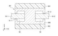
- FIG. 2 is a horizontal cross-sectional view taken along line A-A in FIG. 1.
- This horizontal cross-sectional view shows the reflective panels 10-1 and 10-2 held by the frame 50 in a cross section parallel to the XZ plane.
- the frame 50 has a conductive main body 500 and slits 51-1 and 51-2 formed on both sides of the width of the main body 500.
- the edges of the reflective panels 10-1 and 10-2 are inserted into the slits 51-1 and 51-2, respectively, and are held within a space 52.
- the space 52 is not essential, providing the space 52 allows the weight of the main body 500 of the frame 50 to be reduced and allows for a more flexible holding angle for the reflective panel 10.
- a part of the main body 500 may be formed from a non-conductive material.
- a non-conductive cover 501 such as a resin may be provided on the outer surface of the main body 500, but the cover 501 is not essential. If the cover 501 is provided, the cover 501 functions as a protective member that protects the frame 50.
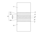
- ⁇ Layer structure of reflective panel> 3 shows an example of a layer structure of the reflective panel 10A.
- This layer structure is a structure in the thickness (Z) direction of the reflective panel 10A.
- the reflective panel 10A has a first substrate 11, a second substrate 12, and an intermediate layer 13A provided between the first substrate 11 and the second substrate 12.
- the intermediate layer 13A is formed by laminating a first intermediate film 131, a second intermediate film 132A, and a third intermediate film 133 in this order.
- the interface between the first intermediate film 131 and the second intermediate film 132A, or the interface between the second intermediate film 132A and the third intermediate film 133 becomes a reflective surface that reflects electromagnetic waves in a predetermined frequency band of 1 GHz to 300 GHz.
- the first substrate 11 and the second substrate 12 support the intermediate layer 13A from both sides.
- the first substrate 11 and the second substrate 12 are insulating polymer sheets or films such as polycarbonate, COP, polyethylene terephthalate (PET), and fluororesin.
- polycarbonate which has excellent impact resistance, durability, and transparency.
- the thicknesses of the first substrate 11 and the second substrate 12 are appropriately selected in the range of 1.0 mm to 10.0 mm.
- the second intermediate film 132A is made of a material containing metal and reflects incident electromagnetic waves.
- the material of the second intermediate film 132A can be stainless steel, mild steel, copper, copper oxide, nickel, nickel oxide, gold, silver, aluminum, or a combination of these.
- the first intermediate film 131 and the third intermediate film 133 are insulating resin films.
- resins that can be used include ethylene vinyl acetate, cycloolefin polymer (COP), ultraviolet-curing resin, thermosetting resin, and thermoplastic resin.
- ultraviolet-curing resins that can be used include urethane-based resin, acrylic-based resin, silicone-based resin, epoxy resin, and urethane acrylate.
- the first intermediate film 131 and the third intermediate film 133 may be made of the same or different materials, but it is desirable to form them from the same material so that the front and back surfaces of the reflective panel 10A can be used with the same reflective properties from either direction without distinguishing between them.
- the relative dielectric constant and dielectric loss tangent of the resin material of the first intermediate film 131 and the third intermediate film 133 are set within an appropriate range to suppress the decrease in reflection efficiency.
- the relative dielectric constant of the above resin material is 2.0 or more and less than 3.0, and the dielectric loss tangent is 0.0001 or more and less than 0.1000. If the relative dielectric constant of the first intermediate film 131 and the third intermediate film 133 is 3.0 or more, there is a risk of increased loss at high frequencies. Similarly, if the dielectric loss tangent of the first intermediate film 131 and the third intermediate film 133 is 0.1000 or more, there is a risk of increased loss of electrical energy in the resin film.
- the average thickness of the first intermediate film 131 is d1 and the average thickness of the third intermediate film 133 is d2, then d1 and d2 satisfy 0.5 ⁇ d1/d2 ⁇ 1.5.
- the average thickness refers to the average thickness measured at 10 points in the width (X) direction of the reflective panel.
- This condition is the film thickness relationship in the finished state of the intermediate layer 13A.
- the position of the second intermediate film 132A in the intermediate layer 13A is stable, and at least one of the reflection efficiency and reflection direction can be maintained well.
- the second intermediate film 132A will be too close to the surface of the intermediate layer 13A, resulting in insufficient coverage by the resin film, and there is a risk of air bubbles being generated at the interface between the intermediate layer 13A and the first substrate 11 or the second substrate 12.
- the resin film covering the second intermediate film 132A may become too thick, which may cause undesirable air bubbles to form inside the dielectric film.
- the second intermediate film 132A is stably maintained in the intermediate layer 13A, and a decrease in reflection efficiency or deterioration in the accuracy of the reflection direction can be suppressed. It is desirable that the value of d1/d2 satisfies 0.5 ⁇ d1/d2 ⁇ 1.5 and is approximately uniform over the entire outer periphery of the reflective panel 10.
- the average thickness of the second intermediate film 132A is d3. From the viewpoint of designing it to be usable for the entire range of 5G or 6G related frequencies and keeping the reflective panel 10 thin, it is desirable that the total thickness of d1, d2, and d3, i.e., the average thickness of the intermediate layer 13A, in the completed state of the intermediate layer 13A, is smaller than the operating wavelength ⁇ (d1 + d2 + d3 ⁇ ⁇ ). For example, when the frequency of the electromagnetic wave incident on the reflective panel 10A is 28.0 GHz, the wavelength ⁇ is 10.7 mm, and it is desirable that the thickness of the intermediate layer 13A is thinner than 10.7 mm.
- FIG. 4 shows an example of the layer structure of the reflective panel 10B.
- the reflective panel 10B has the same layer structure as the reflective panel 10A, except that the second intermediate film 132B of the intermediate layer 13B has an opening 135.
- the intermediate layer 13B is held between the first substrate 11 and the second substrate 12.
- the intermediate layer 13B is formed by laminating the first intermediate film 131, the second intermediate film 132B, and the third intermediate film 133 in this order.
- the interface between the first intermediate film 131 and the second intermediate film 132B, or the interface between the second intermediate film 132B and the third intermediate film 133 becomes a reflective surface that selectively reflects electromagnetic waves in a predetermined frequency band of 1 GHz to 300 GHz.
- the materials, thicknesses, etc. of the first substrate 11, the second substrate 12, the first intermediate film 131, and the third intermediate film 133 are the same as those of the reflective panel 10A.
- the openings 135 of the second intermediate film 132B may be through holes of a square, circle, ellipse, polygon, or the like, or may be mesh openings.
- the openings 135 penetrating the second intermediate film 132B may be formed in a periodic arrangement to enhance the selectivity of reflection for a specific frequency.
- the second intermediate film 132B may be formed in a mesh structure, and the mesh openings may be the openings 135 of the second intermediate film 132B.
- the aperture ratio of the second intermediate film 132B is preferably 50% or more and 80% or less. If the aperture ratio exceeds 80%, the desired reflection efficiency may not be obtained.
- the aperture ratio is less than 50%, the visible light transmittance of the reflection panel 10B may be reduced. If transparency to visible light is not required depending on the usage mode of the reflection panel 10B, the aperture ratio of the openings 135 may be made smaller than 50% to prioritize improvement of the reflection efficiency.
- the first intermediate film 131 and the third intermediate film 133 may be connected within the opening 135 of the second intermediate film 132B.
- the opening 135 does not need to be completely filled with the resin film, and may be 90.0% or more of the total area or volume of the opening 135 depending on the bonding conditions when forming the intermediate layer 13B.
- the first intermediate film 131 and the third intermediate film 133 may enter the opening 135 from both sides of the second intermediate film 132B, or either the first intermediate film 131 or the third intermediate film 133 may enter the opening 135.
- the average thickness d1 of the first intermediate film 131 and the average thickness d2 of the third intermediate film 133 in the finished state also satisfy the condition 0.5 ⁇ d1/d2 ⁇ 1.5. This allows the second intermediate film 132B to be stably held in the intermediate layer 13B, suppressing a decrease in reflection efficiency or deterioration in the accuracy of the reflection direction. Furthermore, assuming that the average thickness of the second intermediate film 132B is d3, the total thickness of d1, d2, and d3, i.e., the thickness of the intermediate layer 13B, is smaller than the operating wavelength ⁇ (d1+d2+d3 ⁇ ).
- samples are prepared under different conditions, and the return loss at a specified frequency is measured to verify the preferred range of the film thickness relationship of the first intermediate film 131, the second intermediate film, and the third intermediate film contained in the intermediate layer 13.
- the return loss is measured using a vector network analyzer and a high-frequency oblique incidence free-space type S-parameter measurement jig.
- As a reference value for return loss the return loss is measured using a smooth aluminum plate that is 3 mm thick and 300 mm x 300 mm, and this measurement value is set to a return loss of 0.00 dB.
- Example 1 is Example 1.
- a sample of a reflective panel 10 is prepared by using a polycarbonate sheet having a thickness of 2 mm as the first substrate 11 and the second substrate 12, and disposing an intermediate layer 13 between the two polycarbonate sheets.
- a first intermediate film 131 is made of ethylene vinyl acetate having a thickness of 400 ⁇ m
- a second intermediate film 132 is made of stainless steel mesh having a thickness of 100 ⁇ m
- a third intermediate film 133 is made of ethylene vinyl acetate having a thickness of 400 ⁇ m.
- the average opening diameter of the stainless steel mesh is 268 ⁇ m, and the average opening ratio is 71%.
- This laminate is sandwiched between two pieces of glass having a thickness of 3 mm, and heated at 130° C. under vacuum for 60 minutes to prepare a reflective panel 10.
- the size of the reflective panel 10 is 1000 mm ⁇ 2000 mm.
- FIG. 5A shows a schematic diagram of the layer structure of the reflective panel of Example 1
- FIG. 5B shows an optical microscope image of the cross section of the sample.
- the average thickness d1 of the first intermediate film 131 is 400 ⁇ m
- the average thickness d3 of the second intermediate film 132 is 100 ⁇ m
- the average thickness d2 of the third intermediate film 133 is 400 ⁇ m.
- d1/d2 1.0, which satisfies the condition 0.5 ⁇ d1/d2 ⁇ 1.5.
- d1+d2+d3 900 ⁇ m.
- Example 2 is Example 2.
- a sample of the reflective panel 10 is prepared by using a polycarbonate sheet having a thickness of 2 mm as the first substrate 11 and the second substrate 12, and disposing the intermediate layer 13 between the two polycarbonate sheets.
- the design conditions of the intermediate layer 13 are the same as those of Example 1, the first intermediate film 131 is ethylene vinyl acetate having a thickness of 400 ⁇ m, the second intermediate film 132 is stainless steel mesh having a thickness of 100 ⁇ m, and the third intermediate film 133 is ethylene vinyl acetate having a thickness of 400 ⁇ m.
- the conditions of the stainless steel mesh are also the same.
- the above-mentioned laminate is sandwiched between two pieces of glass having a thickness of 3 mm, and heated at 90° C. under vacuum for 60 minutes to prepare a sample of Example 2.
- the size of the reflective panel 10 is 1000 mm ⁇ 2000 mm.
- the average thickness d1 of the first intermediate film 131 was 400 ⁇ m
- the average thickness d3 of the second intermediate film 132 was 100 ⁇ m
- the average thickness d2 of the third intermediate film 133 was 350 ⁇ m.
- d1/d2 1.1, which satisfies the condition 0.5 ⁇ d1/d2 ⁇ 1.5.
- d1 + d2 + d3 850 ⁇ m, which also satisfies the condition d1 + d2 + d3 ⁇ ⁇ .
- Example 3 is Example 3.
- a sample of the reflective panel 10 is prepared by using a polycarbonate sheet having a thickness of 2 mm as the first substrate 11 and the second substrate 12, and disposing the intermediate layer 13 between the two polycarbonate sheets.
- the design conditions of the intermediate layer 13 are the same as those of Example 1, the first intermediate film 131 is ethylene vinyl acetate having a thickness of 400 ⁇ m, the second intermediate film 132 is stainless steel mesh having a thickness of 100 ⁇ m, and the third intermediate film 133 is ethylene vinyl acetate having a thickness of 400 ⁇ m.
- the conditions of the stainless steel mesh are also the same.
- the above-mentioned laminate is sandwiched between two pieces of glass having a thickness of 3 mm, and heated at 88° C. under vacuum for 60 minutes to prepare a sample of Example 2.
- the size of the reflective panel 10 is 1000 mm ⁇ 2000 mm.
- the average thickness d1 of the first intermediate film 131 was 400 ⁇ m
- the average thickness d3 of the second intermediate film 132 was 100 ⁇ m
- the average thickness d2 of the third intermediate film 133 was 285 ⁇ m.
- d1/d2 1.4, which satisfies the condition 0.5 ⁇ d1/d2 ⁇ 1.5.
- d1 + d2 + d3 785 ⁇ m, which also satisfies the condition d1 + d2 + d3 ⁇ ⁇ .
- Example 4 is Comparative Example 1.
- the design conditions are the same as those of Examples 1 to 3. That is, a sample of the reflective panel 10 is prepared by using a polycarbonate sheet having a thickness of 2 mm as the first substrate 11 and the second substrate 12, and disposing the intermediate layer 13 between the two polycarbonate sheets.
- the design values of the intermediate layer 13 are ethylene vinyl acetate having a thickness of 400 ⁇ m for the first intermediate film 131, stainless steel mesh having a thickness of 100 ⁇ m for the second intermediate film 132, and ethylene vinyl acetate having a thickness of 400 ⁇ m for the third intermediate film 133.
- the conditions of the stainless steel mesh are also the same.
- the above-mentioned laminate is sandwiched between two pieces of glass having a thickness of 3 mm, and heated at 80° C. under vacuum for 60 minutes to prepare a sample of Example 3.
- the size of the reflective panel 10 is 1000 mm ⁇ 2000 mm.
- the average thickness d1 of the first intermediate film 131 was 400 ⁇ m
- the average thickness d3 of the second intermediate film 132 was 100 ⁇ m
- the average thickness d2 of the third intermediate film 133 was 200 ⁇ m.
- d1/d2 2.0, which is outside the range of 0.5 ⁇ d1/d2 ⁇ 1.5.
- the cross section of the sample in Example 4 was observed with an optical microscope, 25 air bubbles with sizes of about 2 mm to 10 mm were observed within the effective range of 1000 mm x 2000 mm.
- the return loss was measured for an incident electromagnetic wave of 28.0 GHz, it was -1.75 dB compared to an ideal aluminum plate reflector, indicating that the return loss had increased. This is thought to be due to the position of the second intermediate film 132 being offset in the intermediate layer 13, which resulted in the generation of air bubbles in the resin film.
- Example 5 is Comparative Example 2.
- the design conditions are the same as those of Examples 1 to 4, except for the second intermediate film 132.
- a sample of the reflective panel 10 is prepared by using a polycarbonate sheet having a thickness of 2 mm as the first substrate 11 and the second substrate 12, and disposing the intermediate layer 13 between the two polycarbonate sheets.
- the first intermediate film 131 and the third intermediate film of the intermediate layer 13 are ethylene vinyl acetate having a thickness of 400 ⁇ m.
- As the second intermediate film 132 a film in which a sputtered film of Ag-based metal having a thickness of 360 nm is formed on polyethylene terephthalate having a thickness of 100 ⁇ m is used.
- the above-mentioned laminate is sandwiched between two pieces of glass having a thickness of 3 mm, and heated at 130° C. for 60 minutes under vacuum, to prepare a sample of Example 4.
- the size of the reflective panel 10 is 1000 mm ⁇ 2000 mm.
- Figure 6A shows a schematic diagram of the layer structure of the reflective panel of Example 5
- Figure 6B shows an optical microscope image of the cross section of the sample.
- the average thickness d1 of the first intermediate film 131 is 400 ⁇ m
- the average thickness d2 of the third intermediate film 133 is 50 ⁇ m.
- d1/d2 8.0, which is outside the range of 0.5 ⁇ d1/d2 ⁇ 1.5.
- 125 bubbles 101 with sizes of about 2 mm to 10 mm were observed within the effective range of 1000 mm x 2000 mm.
- the average thickness d1 of the first intermediate film 131 and the average thickness d2 of the third intermediate film 133 are configured to satisfy 0.5 ⁇ d1/d2 ⁇ 1.5. Since the film thickness relationship between d1 and d2 is the same even if the first intermediate film 131 and the third intermediate film 133 are reversed, when d1/d2 is smaller than 1.5, d1/d2 is larger than 0.5 when viewed from the opposite side.
- the method of manufacturing the reflective panel 10 is as follows: (a) An intermediate layer 13 in which a first intermediate film 131, a second intermediate film 132, and a third intermediate film 133 are laminated in this order is disposed between a first substrate 11 and a second substrate 12; (b) The first substrate 11, intermediate layer 13, and second substrate 12 are vacuum-pressed together at a temperature higher than 80°C and lower than 130°C, so that the ratio d1/d2 of the average thickness d1 of the first intermediate film 131 to the average thickness d2 of the third intermediate film 133 after pressing satisfies 0.5 ⁇ d1/d2 ⁇ 1.5.
- the condition d1+d2+d3 ⁇ is satisfied. Even if d1+d2+d3 ⁇ is satisfied, if it is outside the range of 0.5 ⁇ d1/d2 ⁇ 1.5, the return loss will increase, making it difficult to maintain the accuracy of the reflection efficiency or reflection direction.
- the electromagnetic wave reflecting device 60 and the electromagnetic wave reflecting fence 100 By using the above-mentioned reflective panel 10 in the electromagnetic wave reflecting device 60 and the electromagnetic wave reflecting fence 100, it is possible to reduce the return loss and maintain at least one of the reflection efficiency and the accuracy of the reflection direction.
- the electromagnetic wave reflecting device and the electromagnetic wave reflecting fence using the reflective panel of the embodiment are effectively used in environments where many blind zones occur within a limited space. If the reflective panel 10 is transparent to visible light, the electromagnetic wave reflecting device and the electromagnetic wave reflecting fence can also be used as a safety fence or a soundproof fence.
- the in-plane size of the reflective panel 10 can be appropriately selected within a range from 30 cm x 30 cm to 3 m x 3 m.
- the entire surface of the reflective panel 10 may be a metasurface, or a portion of it may be a mirror-reflective surface.
- a protective layer such as an ultraviolet protection film on the surfaces of the first substrate 11 and the second substrate of the reflective panel 10, it can be used for a long period of time in outdoor environments.
- the present disclosure may include the following configurations.
- (Item 1) A first substrate; A second substrate; an intermediate layer provided between the first substrate and the second substrate, the intermediate layer being formed by stacking a first intermediate film, a second intermediate film, and a third intermediate film in this order; an interface between the first intermediate film and the second intermediate film, or an interface between the second intermediate film and the third intermediate film, is a reflective surface that reflects electromagnetic waves of 1 GHz or more and 300 GHz or less; If the average thickness of the first interlayer film is d1 and the average thickness of the third interlayer film is d2, 0.5 ⁇ d1/d2 ⁇ 1.5 Meet the reflective panels.
- (Item 2) Item 2.
- the reflective panel according to item 1 wherein the thickness of the intermediate layer is smaller than the wavelength of the electromagnetic wave incident on the reflective surface.
- Item 5 Item 5.
- (Item 7) The reflective panel according to item 6, wherein the aperture ratio of the through holes or the mesh structure is 50.0% or more and 80% or less.
- (Item 8) Item 8. The reflective panel according to item 6 or 7, wherein the first intermediate film and the third intermediate film are connected inside the opening.
- (Item 9) 9. The reflective panel according to any one of items 6 to 8, wherein at least one of the first intermediate film and the third intermediate film is disposed inside the opening.
- Item 10 Item 10. The reflective panel according to item 9, wherein the filling rate of the openings is 90.0% or more of the total area or volume of the openings.
- (Item 11) A reflective panel according to any one of items 1 to 10, A frame for holding the reflective panel; An electromagnetic wave reflecting device having the same.
- An electromagnetic wave reflective fence comprising two or more electromagnetic wave reflective devices according to item 11, the two or more reflective panels being connected by the frame.
- an intermediate layer having a first intermediate film, a second intermediate film, and a third intermediate film laminated in this order is disposed between the first substrate and the second substrate; the first substrate, the intermediate layer, and the second substrate are vacuum-compressed together at a temperature higher than 80° C. and lower than 130° C., so that a ratio d1/d2 of an average thickness d1 of the first intermediate film to an average thickness d2 of the third intermediate film after compression is such that 0.5 ⁇ d1/d2 ⁇ 1.5 is satisfied; How to make a reflective panel.
- Electromagnetic wave reflection device 100
- Air bubble 131
- First intermediate film 132
- Second intermediate film 133
- Third intermediate film 135 Opening d1 Average thickness of first intermediate film d2 Average thickness of third intermediate film
Landscapes
- Physics & Mathematics (AREA)
- Electromagnetism (AREA)
- Engineering & Computer Science (AREA)
- Manufacturing & Machinery (AREA)
- Aerials With Secondary Devices (AREA)
Abstract
Description
前記第1中間膜の平均厚さをd1、前記第3中間膜の平均厚さをd2とすると、
0.5<d1/d2<1.5
を満たす。
図3は、反射パネル10Aの層構成の一例を示す。この層構成は、反射パネル10Aの厚さ(Z)方向の構成である。反射パネル10Aは、第1基板11と、第2基板12と、第1基板11と第2基板12の間に設けられる中間層13Aを有する。中間層13Aは、第1中間膜131、第2中間膜132A、及び第3中間膜133がこの順で積層されている。電磁波の入射方向によって、第1中間膜131と第2中間膜132Aの界面、または第2中間膜132Aと第3中間膜133の界面は、1GHz以上300GHz以下の所定の周波数帯の電磁波を反射する反射面となる。
例1は、実施例1である。第1基板11及び第2基板12として、厚さ2mmのポリカーボネートシートを用い、2枚のポリカーボネートシートの間に中間層13を配置した反射パネル10のサンプルを作製する。中間層13の設計条件として、第1中間膜131は厚さ400μmのエチレン酢酸ビニル、第2中間膜132は厚さ100μmのステンレスメッシュ、第3中間膜133は厚さ400μmのエチレン酢酸ビニルを用いる。ステンレスメッシュの平均開口径は268μm、平均開口率は71%である。この積層体を2枚の厚さ3mmのガラスで挟み、真空下130℃で60分間加熱することで、反射パネル10を作成する。反射パネル10のサイズは1000mm×2000mmである。
例2は、実施例2である。第1基板11及び第2基板12として、厚さ2mmのポリカーボネートシートを用い、2枚のポリカーボネートシートの間に中間層13を配置した反射パネル10のサンプルを作製する。中間層13の設計条件は例1と同じであり、第1中間膜131は厚さ400μmのエチレン酢酸ビニル、第2中間膜132は厚さ100μmのステンレスメッシュ、第3中間膜133は厚さ400μmのエチレン酢酸ビニルである。ステンレスメッシュの条件も同じである。貼り合わせプロセスで、上述した積層体を厚さ3mmの2枚のガラスの間に挟み、真空下90℃で60分間加熱して、例2のサンプルを作製する。反射パネル10のサイズは1000mm×2000mmである。
例3は、実施例3である。第1基板11及び第2基板12として、厚さ2mmのポリカーボネートシートを用い、2枚のポリカーボネートシートの間に中間層13を配置した反射パネル10のサンプルを作製する。中間層13の設計条件は例1と同じであり、第1中間膜131は厚さ400μmのエチレン酢酸ビニル、第2中間膜132は厚さ100μmのステンレスメッシュ、第3中間膜133は厚さ400μmのエチレン酢酸ビニルである。ステンレスメッシュの条件も同じである。貼り合わせプロセスで、上述した積層体を厚さ3mmの2枚のガラスの間に挟み、真空下88℃で60分間加熱して、例2のサンプルを作製する。反射パネル10のサイズは1000mm×2000mmである。
例4は、比較例1である。設計条件は、例1から例3と同じである。すなわち、第1基板11及び第2基板12として、厚さ2mmのポリカーボネートシートを用い、2枚のポリカーボネートシートの間に中間層13を配置した反射パネル10のサンプルを作製する。中間層13の設計値は、第1中間膜131は厚さ400μmのエチレン酢酸ビニル、第2中間膜132は厚さ100μmのステンレスメッシュ、第3中間膜133は厚さ400μmのエチレン酢酸ビニルである。ステンレスメッシュの条件も同じである。貼り合わせプロセスでは、上述した積層体を厚さ3mmの2枚のガラスの間に挟み、真空下80℃で60分間加熱して、例3のサンプルを作製する。反射パネル10のサイズは1000mm×2000mmである。
例5は、比較例2である。設計条件は、第2中間膜132を除いて、例1から例4と同じである。第1基板11及び第2基板12として、厚さ2mmのポリカーボネートシートを用い、2枚のポリカーボネートシートの間に中間層13を配置した反射パネル10のサンプルを作製する。中間層13の第1中間膜131と第3中間膜は、厚さ400μmのエチレン酢酸ビニルである。第2中間膜132として、厚さ100μmのポリエチレンテレフタラートに厚さ360nmのAg系金属のスパッタ膜が形成された膜を用いる。上述した積層体を厚さ3mmの2枚のガラスの間に挟み、真空下130℃60分間加熱して、例4のサンプルを作製する。反射パネル10のサイズは1000mm×2000mmである。
(a)第1基板11と第2基板12の間に、第1中間膜131、第2中間膜132、及び第3中間膜133がこの順で積層された中間層13を配置し、
(b)第1基板11と中間層13と第2基板12を、80℃より高く130℃以下の温度で真空圧着して、圧着後の第3中間膜133の平均厚さd2に対する第1中間膜131の平均厚さd1の比d1/d2が0.5<d1/d2<1.5を満たすようにする。
(項1)
第1基板と、
第2基板と、
前記第1基板と前記第2基板の間に設けられる中間層であって、第1中間膜、第2中間膜、及び第3中間膜がこの順で積層された中間層と、
を有し、前記第1中間膜と前記第2中間膜の界面、または前記第2中間膜と前記第3中間膜の界面は1GHz以上300GHz以下の電磁波を反射する反射面であり、
前記第1中間膜の平均厚さをd1、前記第3中間膜の平均厚さをd2とすると、
0.5<d1/d2<1.5
を満たす、反射パネル。
(項2)
前記中間層の厚さは前記反射面に入射する前記電磁波の波長よりも小さい、項1に記載の反射パネル。
(項3)
前記第1中間膜と前記第3中間膜は樹脂層である、項1または2に記載の反射パネル。
(項4)
前記樹脂層の比誘電率は2.0以上3.0以下、誘電正接は0.0001以上0.1000未満である、項3に記載の反射パネル。
(項5)
前記第2中間膜は金属を含む膜である、項1から4のいずれかに記載の反射パネル。
(項6)
前記第2中間膜は貫通穴またはメッシュ構造の開口を有する、項5に記載の反射パネル。
(項7)
前記貫通穴または前記メッシュ構造の開口率は50.0%以上80%以下である、項6に記載の反射パネル。
(項8)
前記第1中間膜と前記第3中間膜は前記開口の内部で接続されている、項6または7に記載の反射パネル。
(項9)
前記開口の内部に前記第1中間膜と前記第3中間膜の少なくとも一方が入っている、項6から8のいずれかに記載の反射パネル。
(項10)
前記開口の充填率は、前記開口の総面積または総体積の90.0%以上である、項9に記載の反射パネル。
(項11)
項1から10のいずれかに記載の反射パネルと、
前記反射パネルを保持するフレームと、
を有する電磁波反射装置。
(項12)
項11に記載の電磁波反射装置を2以上有し、2以上の前記反射パネルを前記フレームによって連結した電磁波反射フェンス。
(項13)
第1基板と第2基板の間に、第1中間膜、第2中間膜、及び第3中間膜がこの順で積層された中間層を配置し、
前記第1基板と前記中間層と前記第2基板を、80℃より高く130℃以下の温度で真空圧着して、圧着後の前記第3中間膜の平均厚さd2に対する前記第1中間膜の平均厚さd1の比d1/d2が0.5<d1/d2<1.5を満たすようにする、
反射パネルの作製方法。
11 第1基板
12 第2基板
13、13A、13B 中間層
50 フレーム(サイドフレーム)
57 トップフレーム
58 ボトムフレーム
60、60-1、60-2、60-3 電磁波反射装置
100 電磁波反射フェンス
101 気泡
131 第1中間膜
132 第2中間膜
133 第3中間膜
135 開口
d1 第1中間膜の平均厚さ
d2 第3中間膜の平均厚さ
Claims (13)
- 第1基板と、
第2基板と、
前記第1基板と前記第2基板の間に設けられる中間層であって、第1中間膜、第2中間膜、及び第3中間膜がこの順で積層された中間層と、
を有し、前記第1中間膜と前記第2中間膜の界面、または前記第2中間膜と前記第3中間膜の界面は1GHz以上300GHz以下の電磁波を反射する反射面であり、
前記第1中間膜の平均厚さをd1、前記第3中間膜の平均厚さをd2とすると、
0.5<d1/d2<1.5
を満たす、反射パネル。 - 前記中間層の厚さは、前記反射面に入射する前記電磁波の波長よりも小さい、
請求項1に記載の反射パネル。 - 前記第1中間膜と前記第3中間膜は樹脂層である、
請求項1に記載の反射パネル。 - 前記樹脂層の比誘電率は2.0以上3.0以下、誘電正接は0.0001以上0.1000未満である、
請求項3に記載の反射パネル。 - 前記第2中間膜は金属を含む膜である、
請求項1に記載の反射パネル。 - 前記第2中間膜は貫通穴またはメッシュ構造の開口を有する、
請求項5に記載の反射パネル。 - 前記貫通穴または前記メッシュ構造の開口率は50.0%以上80%以下である、
請求項6に記載の反射パネル。 - 前記第1中間膜と前記第3中間膜は前記開口の内部で接続されている、
請求項6に記載の反射パネル。 - 前記開口の内部に前記第1中間膜と前記第3中間膜の少なくとも一方が入っている、
請求項6に記載の反射パネル。 - 前記開口の充填率は、前記開口の総面積または総体積の90.0%以上である、
請求項9に記載の反射パネル。 - 請求項1から10のいずれか一項に記載の反射パネルと、
前記反射パネルを保持するフレームと、
を有する電磁波反射装置。 - 請求項11に記載の電磁波反射装置を2以上有し、2以上の前記反射パネルを前記フレームによって連結した電磁波反射フェンス。
- 第1基板と第2基板の間に、第1中間膜、第2中間膜、及び第3中間膜がこの順で積層された中間層を配置し、
前記第1基板と前記中間層と前記第2基板を、80℃より高く130℃以下の温度で真空圧着して、圧着後の前記第3中間膜の平均厚さd2に対する前記第1中間膜の平均厚さd1の比d1/d2が0.5<d1/d2<1.5を満たすようにする、
反射パネルの作製方法。
Priority Applications (3)
| Application Number | Priority Date | Filing Date | Title |
|---|---|---|---|
| CN202380067180.2A CN119895663A (zh) | 2022-09-26 | 2023-08-29 | 反射面板、使用其的电磁波反射装置、电磁波反射围栏以及反射面板的制作方法 |
| JP2024549900A JPWO2024070407A1 (ja) | 2022-09-26 | 2023-08-29 | |
| US19/079,975 US20250210877A1 (en) | 2022-09-26 | 2025-03-14 | Reflective panel, electromagnetic wave reflecting apparatus using reflective panel, electromagnetic wave reflecting fence, and method of making reflective panel |
Applications Claiming Priority (2)
| Application Number | Priority Date | Filing Date | Title |
|---|---|---|---|
| JP2022-152154 | 2022-09-26 | ||
| JP2022152154 | 2022-09-26 |
Related Child Applications (1)
| Application Number | Title | Priority Date | Filing Date |
|---|---|---|---|
| US19/079,975 Continuation US20250210877A1 (en) | 2022-09-26 | 2025-03-14 | Reflective panel, electromagnetic wave reflecting apparatus using reflective panel, electromagnetic wave reflecting fence, and method of making reflective panel |
Publications (1)
| Publication Number | Publication Date |
|---|---|
| WO2024070407A1 true WO2024070407A1 (ja) | 2024-04-04 |
Family
ID=90477138
Family Applications (1)
| Application Number | Title | Priority Date | Filing Date |
|---|---|---|---|
| PCT/JP2023/031165 Ceased WO2024070407A1 (ja) | 2022-09-26 | 2023-08-29 | 反射パネル、これを用いた電磁波反射装置、電磁波反射フェンス、及び反射パネルの作製方法 |
Country Status (5)
| Country | Link |
|---|---|
| US (1) | US20250210877A1 (ja) |
| JP (1) | JPWO2024070407A1 (ja) |
| CN (1) | CN119895663A (ja) |
| TW (1) | TW202414895A (ja) |
| WO (1) | WO2024070407A1 (ja) |
Citations (2)
| Publication number | Priority date | Publication date | Assignee | Title |
|---|---|---|---|---|
| WO2021199504A1 (ja) * | 2020-03-31 | 2021-10-07 | Agc株式会社 | 無線伝達システム |
| WO2022163813A1 (ja) * | 2021-01-29 | 2022-08-04 | 積水化学工業株式会社 | 構造体、及び建築材料 |
-
2023
- 2023-08-29 CN CN202380067180.2A patent/CN119895663A/zh active Pending
- 2023-08-29 WO PCT/JP2023/031165 patent/WO2024070407A1/ja not_active Ceased
- 2023-08-29 JP JP2024549900A patent/JPWO2024070407A1/ja active Pending
- 2023-08-31 TW TW112132931A patent/TW202414895A/zh unknown
-
2025
- 2025-03-14 US US19/079,975 patent/US20250210877A1/en active Pending
Patent Citations (2)
| Publication number | Priority date | Publication date | Assignee | Title |
|---|---|---|---|---|
| WO2021199504A1 (ja) * | 2020-03-31 | 2021-10-07 | Agc株式会社 | 無線伝達システム |
| WO2022163813A1 (ja) * | 2021-01-29 | 2022-08-04 | 積水化学工業株式会社 | 構造体、及び建築材料 |
Also Published As
| Publication number | Publication date |
|---|---|
| JPWO2024070407A1 (ja) | 2024-04-04 |
| TW202414895A (zh) | 2024-04-01 |
| US20250210877A1 (en) | 2025-06-26 |
| CN119895663A (zh) | 2025-04-25 |
Similar Documents
| Publication | Publication Date | Title |
|---|---|---|
| CN112622391B (zh) | 一种光学透明超宽带雷达与红外双隐身结构 | |
| US11967769B2 (en) | Planar antenna, layered antenna structure, and window glass for vehicle | |
| Zheng et al. | Transparent broadband absorber based on a multilayer ITO conductive film | |
| WO2019107514A1 (ja) | アンテナユニット、およびアンテナ付きガラス板 | |
| US12057631B2 (en) | Antenna unit and window glass | |
| US20250055201A1 (en) | Electromagnetic wave reflecting device, electromagnetic wave reflecting fence, and reflection panel | |
| KR20220058481A (ko) | 메타표면을 포함하는 전자기파 흡수체 | |
| EP2738875B1 (en) | Cassegrain microwave antenna | |
| US20250210877A1 (en) | Reflective panel, electromagnetic wave reflecting apparatus using reflective panel, electromagnetic wave reflecting fence, and method of making reflective panel | |
| CN102842760B (zh) | 透波材料及其天线罩和天线系统 | |
| CN114927880B (zh) | 一种吸波单元及吸波超表面 | |
| JP2017181911A (ja) | 電波透過性赤外線反射積層体および閉鎖部材 | |
| KR20250018469A (ko) | 전자파 반사 장치, 전자파 반사 펜스 및 반사 패널 | |
| WO2020189350A1 (ja) | 電波吸収体及び電波吸収体用キット | |
| CN114465016A (zh) | 一种用于x频段隐身的超薄透光超材料吸波体 | |
| WO2024214369A1 (ja) | 電磁波反射パネル、電磁波反射装置、及び電磁波反射フェンス | |
| WO2026105746A1 (ja) | 電磁波吸収体 | |
| WO2024195270A1 (ja) | 電磁波反射パネル、電磁波反射装置、電磁波反射フェンス、及び電磁波反射パネルの製造方法 | |
| CN119029558B (zh) | 一种雷达rcs缩减和红外发射率可调兼容的隐身超表面 | |
| WO2024214372A1 (ja) | 電磁波反射パネルの製造方法、電磁波反射パネル、電磁波反射装置、及び電磁波反射フェンス | |
| JP2025147893A (ja) | メタサーフェスシート及び窓構造 | |
| WO2024070455A1 (ja) | 反射パネル、これを用いた電磁波反射装置、電磁波反射フェンス、及び反射パネルの作製方法 | |
| CN119156746A (zh) | 电磁波反射装置、电磁波反射围栏以及反射面板 | |
| WO2024241666A1 (ja) | 電磁波反射パネル、電磁波反射装置、及び電磁波反射フェンス | |
| JP2018002534A (ja) | 合わせガラスおよび閉鎖部材 |
Legal Events
| Date | Code | Title | Description |
|---|---|---|---|
| 121 | Ep: the epo has been informed by wipo that ep was designated in this application |
Ref document number: 23871648 Country of ref document: EP Kind code of ref document: A1 |
|
| WWE | Wipo information: entry into national phase |
Ref document number: 2024549900 Country of ref document: JP |
|
| WWE | Wipo information: entry into national phase |
Ref document number: 202380067180.2 Country of ref document: CN |
|
| WWP | Wipo information: published in national office |
Ref document number: 202380067180.2 Country of ref document: CN |
|
| NENP | Non-entry into the national phase |
Ref country code: DE |
|
| 122 | Ep: pct application non-entry in european phase |
Ref document number: 23871648 Country of ref document: EP Kind code of ref document: A1 |