WO2024070295A1 - ベルト - Google Patents
ベルト Download PDFInfo
- Publication number
- WO2024070295A1 WO2024070295A1 PCT/JP2023/029584 JP2023029584W WO2024070295A1 WO 2024070295 A1 WO2024070295 A1 WO 2024070295A1 JP 2023029584 W JP2023029584 W JP 2023029584W WO 2024070295 A1 WO2024070295 A1 WO 2024070295A1
- Authority
- WO
- WIPO (PCT)
- Prior art keywords
- rfid tag
- belt
- dielectric layer
- radiating element
- layer
- Prior art date
- Legal status (The legal status is an assumption and is not a legal conclusion. Google has not performed a legal analysis and makes no representation as to the accuracy of the status listed.)
- Ceased
Links
Images



Classifications
-
- B—PERFORMING OPERATIONS; TRANSPORTING
- B29—WORKING OF PLASTICS; WORKING OF SUBSTANCES IN A PLASTIC STATE IN GENERAL
- B29D—PRODUCING PARTICULAR ARTICLES FROM PLASTICS OR FROM SUBSTANCES IN A PLASTIC STATE
- B29D29/00—Producing belts or bands
-
- F—MECHANICAL ENGINEERING; LIGHTING; HEATING; WEAPONS; BLASTING
- F16—ENGINEERING ELEMENTS AND UNITS; GENERAL MEASURES FOR PRODUCING AND MAINTAINING EFFECTIVE FUNCTIONING OF MACHINES OR INSTALLATIONS; THERMAL INSULATION IN GENERAL
- F16G—BELTS, CABLES, OR ROPES, PREDOMINANTLY USED FOR DRIVING PURPOSES; CHAINS; FITTINGS PREDOMINANTLY USED THEREFOR
- F16G1/00—Driving-belts
-
- F—MECHANICAL ENGINEERING; LIGHTING; HEATING; WEAPONS; BLASTING
- F16—ENGINEERING ELEMENTS AND UNITS; GENERAL MEASURES FOR PRODUCING AND MAINTAINING EFFECTIVE FUNCTIONING OF MACHINES OR INSTALLATIONS; THERMAL INSULATION IN GENERAL
- F16G—BELTS, CABLES, OR ROPES, PREDOMINANTLY USED FOR DRIVING PURPOSES; CHAINS; FITTINGS PREDOMINANTLY USED THEREFOR
- F16G1/00—Driving-belts
- F16G1/06—Driving-belts made of rubber
- F16G1/08—Driving-belts made of rubber with reinforcement bonded by the rubber
- F16G1/10—Driving-belts made of rubber with reinforcement bonded by the rubber with textile reinforcement
-
- F—MECHANICAL ENGINEERING; LIGHTING; HEATING; WEAPONS; BLASTING
- F16—ENGINEERING ELEMENTS AND UNITS; GENERAL MEASURES FOR PRODUCING AND MAINTAINING EFFECTIVE FUNCTIONING OF MACHINES OR INSTALLATIONS; THERMAL INSULATION IN GENERAL
- F16G—BELTS, CABLES, OR ROPES, PREDOMINANTLY USED FOR DRIVING PURPOSES; CHAINS; FITTINGS PREDOMINANTLY USED THEREFOR
- F16G1/00—Driving-belts
- F16G1/06—Driving-belts made of rubber
- F16G1/08—Driving-belts made of rubber with reinforcement bonded by the rubber
- F16G1/12—Driving-belts made of rubber with reinforcement bonded by the rubber with metal reinforcement
-
- G—PHYSICS
- G06—COMPUTING OR CALCULATING; COUNTING
- G06K—GRAPHICAL DATA READING; PRESENTATION OF DATA; RECORD CARRIERS; HANDLING RECORD CARRIERS
- G06K19/00—Record carriers for use with machines and with at least a part designed to carry digital markings
- G06K19/06—Record carriers for use with machines and with at least a part designed to carry digital markings characterised by the kind of the digital marking, e.g. shape, nature, code
- G06K19/067—Record carriers with conductive marks, printed circuits or semiconductor circuit elements, e.g. credit or identity cards also with resonating or responding marks without active components
- G06K19/07—Record carriers with conductive marks, printed circuits or semiconductor circuit elements, e.g. credit or identity cards also with resonating or responding marks without active components with integrated circuit chips
- G06K19/077—Constructional details, e.g. mounting of circuits in the carrier
Definitions
- the present invention relates to a belt, and more specifically, to a belt equipped with an RFID tag.
- Transmission belts and conveyor belts are used in various products that have belt drive systems.
- Transmission belts and conveyor belts are usually made endless, and are used by being wound around multiple pulleys, including a drive pulley and a driven pulley.
- the belt may not be endless, but may be used in the form of a strip. Even in such cases, the belt is often used by being wound around pulleys.
- belt drive systems are usually inspected to prevent accidents caused by breakdowns. For example, the condition of the belt is inspected periodically to prevent accidents caused by belt damage.
- RFID tags are equipped with an IC chip and a radiating element connected to the IC chip, and are configured to be able to transmit information in the IC chip via wireless communication with an RFID reader/writer.
- RFID reader/writer an RFID reader/writer
- Patent Document 1 describes a transmission belt that includes an RFID tag and a pressure sensor connected to the RFID tag, and is configured to store data detected by the pressure sensor in the memory of an IC chip. It also proposes using the pressure data read from the RFID tag by an RFID reader/writer as information for checking the condition of the belt.
- the belts described above are provided with a core layer to provide tensile strength.
- One such core layer is known to be made of carbon fiber.
- Belts with a core layer made of carbon fiber are highly durable and are suitable for use as transmission belts that are subject to high loads, such as in machine tools and large agricultural machinery.
- the present invention aims to provide a belt with which an RFID tag can communicate even if the core layer is made of a material that exhibits electrical conductivity.
- the belt according to the present invention comprises:
- the present invention comprises a belt body and an RFID tag provided on the belt body,
- the belt body has a core layer made of a conductive material, preferably a core layer made of carbon fiber or a metal material
- the RFID tag is any one of the following types A to C of RFID tags:
- Type A An RFID tag comprising a dielectric layer, a radiating element formed in a loop shape from the front surface to the back surface of the dielectric layer, and an IC chip connected to the radiating element.
- Type B An RFID tag comprising a dielectric layer, a radiating element formed on the front surface of the dielectric layer, a ground conductor formed on the back surface of the dielectric layer, and an IC chip connected to the radiating element.
- Type C An RFID tag comprising a dielectric layer, a radiating element formed on the front surface of the dielectric layer, and a metal layer formed on the back surface of the dielectric layer for reflecting electromagnetic waves from the front surface side of the dielectric layer toward the
- the RFID tag when the RFID tag is an RFID tag of type B, Two connection portions are provided on the dielectric layer to electrically connect the radiating element and the ground conductor, The radiating element, the two connecting portions, and the ground conductor constitute an inverted-F antenna.
- the RFID tag in the belt communicates in the UHF band.
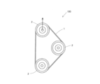
- FIG. 1 is a schematic diagram of a belt drive system including a belt according to one embodiment.
- 1 is a schematic cross-sectional view of a belt according to one embodiment.
- FIG. 2 is a perspective view of an example of a type A RFID tag.
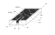
- FIG. 2 is a perspective view of an example of a Type B RFID tag.
- 13 is a schematic cross-sectional view of a modified example of a type B RFID tag.
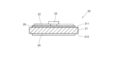
- FIG. 2 is a schematic cross-sectional view of an example Type C RFID tag.
- the belt 1 of this embodiment constitutes a belt drive system 100.
- the belt drive system 100 includes a plurality of pulleys 2 and a belt 1 wound around the plurality of pulleys 2.
- the belt 1 of this embodiment is a transmission belt used to transmit power between pulleys.
- the belt 1 of this embodiment has a length direction, a width direction perpendicular to the length direction, and a thickness direction perpendicular to both the length direction and the width direction.
- the belt 1 of this embodiment is endless and has an inner peripheral surface that contacts the pulley when it is wound around the pulley, and an outer peripheral surface that is the surface opposite the inner peripheral surface.
- the belt 1 of this embodiment includes a belt body 10 made of multiple rubber layers overlapping in the thickness direction, and an RFID tag 20 embedded in the belt body 10.
- the belt body 10 of this embodiment has multiple protrusions that protrude inward. That is, the belt body 10 of this embodiment has multiple protrusions on the inner peripheral surface side. The multiple protrusions are provided at a constant pitch in the longitudinal direction. In addition, recesses are formed between adjacent protrusions. The belt body 10 of this embodiment has a shape on the inner peripheral surface side in which protrusions and recesses are alternately repeated in the longitudinal direction (circumferential direction). Note that the belt of the present invention is not limited to one having a belt body of the type described herein.
- the belt body 10 of this embodiment has an inner rubber layer 11 having teeth 111 that mesh with each pulley 2, an outer rubber layer 12 that forms the outer peripheral surface, and a core layer 13 composed of a carbon fiber core wire 131.
- the belt body 10 of this embodiment also has a reinforcing layer 14 that reinforces the inner rubber layer 11.
- the reinforcing layer 14 forms the inner peripheral surface of the belt body 10.
- the belt 1 exemplified in this embodiment is a toothed belt having a plurality of teeth, and the teeth of the toothed belt are composed of the tooth portion 111 of the inner rubber layer 11 and the reinforcing layer 14 that covers the tooth portion 111 from the inner circumferential side so as to follow the uneven shape of the inner circumferential side of the inner rubber layer 11.
- the outer rubber layer 12 is formed in a strip shape.
- the rubber components of the rubber composition forming the inner rubber layer 11 and the outer rubber layer 12 include, for example, natural rubber (NR), butadiene rubber (BR), styrene-butadiene rubber (SBR), ethylene-propylene rubber (EPR), ethylene-propylene-diene rubber (EPDM), isoprene rubber (IR), acrylonitrile-butadiene rubber (NBR), hydrogenated nitrile rubber (HNBR), isobutylene-isoprene rubber (IIR), chloroprene rubber (CR), chlorosulfonated polyethylene rubber (CSM), chlorinated butyl rubber (CIIR), brominated butyl rubber (BIIR), silicone rubber (SR), urethane rubber (UR), acrylic rubber (ACR), fluororubber (FR), etc.
- the rubber components may be used alone or in combination.
- the rubber composition may contain additives other than the rubber component.
- additives include fillers such as carbon black, silica, calcium carbonate, etc., flame retardants such as ethylene bistetrabromophthalimide, crosslinking agents such as sulfur and organic peroxides, vulcanization accelerators such as zinc oxide, plasticizers such as dioctyl adipate, hardness regulators such as paraffin oil, anti-aging agents such as benzimidazole compounds, lubricants, etc.
- the dielectric constant of the inner rubber layer 11 and the outer rubber layer 12 is preferably 1 or more and 30 or less, and more preferably 10 or more and 30 or less.
- the dielectric constant of each rubber layer means the dielectric constant at 909 MHz, and can be measured by the following measurement method. First, an impedance analyzer (manufactured by HEWLETT PACKARD, model number 4291B RF) is used as the measurement device. Then, the thickness (measured with a micrometer) of a test piece (thickness 3 mm or less, ⁇ 15 mm or more) cut from each rubber layer is input into the measurement device.
- test piece is set in the high impedance test head measurement unit, and a graph of the dielectric constant from 1 MHz to 1 GHz is obtained.
- the dielectric constant at 909 MHz is read from this graph and used as the dielectric constant of each rubber layer.
- the core layer 13 of this embodiment is composed of a core wire 131 made of carbon fiber, as described above.
- the core layer 13 is a layer that exhibits electrical conductivity due to the carbon fiber.
- the fibers that make up the core wire may include synthetic fibers such as polyester fiber, polyamide fiber, and aramid fiber, as well as glass fiber, in addition to carbon fiber.
- the mass ratio of carbon fiber to the total mass of the fibers that make up the core wire is preferably 50 mass% or more, and more preferably 90 mass% or more.
- the core wire 131 of this embodiment is composed only of carbon fiber.
- the core layer may also be composed of canvas.
- the reinforcing layer 14 is made of a fabric material such as a woven fabric, knitted fabric, or nonwoven fabric made from threads such as cotton, polyamide fiber, polyester fiber, or aramid fiber.
- the belt drive system 100 of this embodiment is equipped with an RFID reader/writer (which may be an RFID reader) that is arranged to face the outer circumferential surface of the belt body 10.
- the belt drive system 100 of this embodiment uses electromagnetic waves of 860 to 960 MHz, i.e., electromagnetic waves in the UHF band, to send and receive data.
- the RFID tag 20 of this embodiment is a type A RFID tag.
- the RFID tag 20 includes a dielectric layer 21 extending along the core layer 13, a radiating element 22 formed in a loop shape from a front surface 211 to a back surface 212 of the dielectric layer 21, and an IC chip 23 mounted on the front surface 211 of the dielectric layer 21 and connected to the radiating element 22.
- the type A RFID tag 20 includes the dielectric layer 21, the IC chip 23 mounted on the front surface 211 of the dielectric layer 21, and the radiating element 22 formed on the dielectric layer 21 and formed in a loop shape via the IC chip 23.
- the dielectric layer 21 of type A is made of resin.
- the resin include polyethylene terephthalate (PET), epoxy resin, ABS resin, polycarbonate, polyvinyl chloride (PVC), polytetrafluoroethylene (PTFE), polyphenylene ether (PPE), etc.
- the dielectric constant (909 MHz) of the dielectric layer of type A is preferably 4 to 20, and more preferably 4 to 15. The dielectric constant can be measured in the same manner as the dielectric constant of the inner rubber layer 11 and the outer rubber layer 12.
- the radiating element 22 can be formed by adhering a metal wire or metal foil to the surface 211 of the dielectric layer 21, applying conductive ink to the dielectric layer 21, etching the dielectric layer 21, or the like.
- the metal include copper, aluminum, and silver.
- the radiating element 22 constitutes a loop antenna together with the dielectric layer 21. That is, the radiating element 22 structurally has a pair of surface patterns 221 extending in opposite directions from the IC chip 23 mounted on the surface 211 of the dielectric layer 21, a pair of side patterns 222 formed on each side of the dielectric layer 21, and a back pattern 223 formed on the back surface 212 of the dielectric layer 21.
- the surface pattern 221, the side pattern 222, and the back pattern 223 are connected to each other without interruption, thereby constituting a loop antenna together with the dielectric layer 21.
- the RFID tag 20 is embedded in the outer rubber layer 12 of the belt body 10 so that the back pattern 223 of the radiating element 22 faces the core layer 13.
- the RFID tag 20 is embedded in the outer rubber layer 12 so that the back surface 212 of the dielectric layer 21 faces the core layer 13.
- This allows the RFID tag 20 to communicate with an RFID reader/writer even in a belt 1 in which the core layer 13 is made of carbon fiber, as in the belt 1 of this embodiment.
- the RFID tag 20 in the belt 1 of this embodiment employs a loop antenna, communication using electromagnetic waves over a relatively wide range in the UHF band is possible.
- the IC chip 23 has a pair of terminals electrically connected to the radiating element 22. That is, the IC chip 23 is electrically connected to the radiating element 22 via the pair of terminals.
- the radiating element 22 is configured to generate a current due to electromagnetic waves from an RFID reader/writer, and the IC chip 23 is impedance-matched with the radiating element 22 so that it is driven by this current. That is, the RFID tag 20 of this embodiment is a passive type.
- the IC chip 23 also has a memory that stores data such as information regarding the state of the belt 1.
- the IC chip 23 is configured to receive data transmitted from an RFID reader/writer and transmit information stored in the memory to the RFID reader/writer.
- the RFID tag may be an active type equipped with a battery.
- the IC chip of this embodiment is a sensor-integrated IC chip, and includes a temperature sensor and a control circuit that controls the operation of the temperature sensor.
- the temperature sensor and the control circuit are electrically connected by wiring.
- the wiring is also attached to the temperature sensor and the control circuit by a conductive adhesive.
- the conductive adhesive contains metal particles such as silver particles and a curable resin such as epoxy resin or acrylic resin.
- the IC chip does not have to include a temperature sensor, and instead, the belt 1 may include a temperature sensor outside the IC chip that is electrically connected to the IC chip.
- the temperature sensor is composed of a thermistor whose resistance value changes with temperature change.
- the thermistor may be an NTC thermistor or a CTR thermistor whose resistance value decreases with increasing temperature, or a PTC thermistor whose resistance value increases with increasing temperature.
- the temperature sensor is configured to output a voltage or current according to the change in the resistance value of the thermistor.
- the IC chip of this embodiment is configured to convert the numerical value of the voltage or current output by the temperature sensor into a temperature value by the control circuit.
- the temperature sensor may be composed of a thermocouple.
- the thermocouple is a pair of two metal wires with different components connected together, and outputs a thermoelectromotive force according to temperature change at the connection point of these metal wires.
- Type B and Type C RFID tags that can be used in the present invention.
- the RFID tag 20 of type B includes a dielectric layer 21 extending along the core layer 13, a plate-shaped radiating element 22 formed on the front surface 211 of the dielectric layer 21, a plate-shaped ground conductor 24 formed on the back surface 212 of the dielectric layer 21, and an IC chip 23 connected to the radiating element 22 via a microstrip line 25 and connected to the ground conductor 24 via a connection portion 26. That is, the RFID tag of type B includes a patch antenna (microstrip antenna) composed of the dielectric layer 21, the radiating element 22, and the ground conductor 24. The ground conductor 24 is disposed so as to face the radiating element 22 via the dielectric layer 21. Usually, the area of the ground conductor 24 is larger than the area of the radiating element 22.
- the dielectric constant (909 MHz) of the dielectric layer 21 of type B is preferably greater than 1, more preferably 4 to 20, and more preferably 4 to 15.
- the dielectric constant can be measured in the same manner as the dielectric constant of the inner rubber layer 11 and the outer rubber layer 12. This allows the tag to be made smaller, and reduces damage to the belt body 10 caused by the tag.
- the material constituting the dielectric layer 21 may be, for example, polyphenylene sulfide (PPS resin), polyether ether ketone (PEEK resin), fluorine-based resin, polyethylene terephthalate (PET), epoxy resin, ABS resin, polycarbonate, polyvinyl chloride (PVC), polytetrafluoroethylene (PTFE), polyphenylene ether (PPE), or a ceramic material such as alumina.
- PPS resin polyphenylene sulfide
- PEEK resin polyether ether ketone
- fluorine-based resin polyethylene terephthalate
- PET polyethylene terephthalate
- PET polyethylene terephthalate
- PET polycarbonate
- PVC polyvinyl chloride
- PTFE polytetrafluoroethylene
- PPE polyphenylene ether
- a ceramic material such as alumina.
- the radiating element 22 has a first region 224 to which the microstrip line 25 is connected, and a second region 225 connected to the first region 224 on the side opposite the microstrip line 25. Between the first region 224 and the second region 225, a pair of slits 226 are formed, which extend perpendicular to the microstrip line 25.
- the IC chip 23 is mounted on the side of the dielectric layer 21.
- the IC chip 23 may be mounted on the front or back surface of the dielectric layer 21, or may be embedded in the dielectric layer 21.
- the modified version of the tag of type B includes a dielectric layer 21 extending along the core layer 13, a plate-shaped radiating element 22 formed on the front surface 211 of the dielectric layer 21, a plate-shaped ground conductor 24 formed on the back surface 212 of the dielectric layer 21, an IC chip 23 mounted on the radiating element 22 or the ground conductor 24, a short-circuit wire 26 that extends through the dielectric layer 21 and serves as a connection portion connecting the radiating element 22 and the ground conductor 24, and a power supply line 27 that extends through the dielectric layer 21 and serves as a connection portion connecting the radiating element 22 and the ground conductor 24.
- Each of the short circuit line 26 and the power supply line 27 is formed by a conductive paste filled in a through hole formed in the dielectric layer 21.
- the RFDI tag of the modified type B has an inverted F antenna composed of the radiating element 22, the ground conductor 24, and the connection portion (the short-circuit wire 26 and the power supply line 27). This allows the tag to be compact while still enabling communication over a relatively wide range of electromagnetic waves in the UHF band.
- the IC chip 23 may be embedded in the dielectric layer 21, similar to the short-circuit wire 26 and the power supply line 27. This prevents poor contact at the terminals of the IC chip and at each connection portion caused by bending of the belt body 10.
- a slit is formed in the radiating element 22 or the ground conductor 24, and the IC chip 23 is provided in the slit.
- a pair of terminals of the IC chip 23 may both be electrically connected to the radiating element 22, or one terminal may be electrically connected to the radiating element 22 and the other terminal may be electrically connected to the ground conductor 24. Since the electromagnetic field of such an RFID tag is enhanced in the vicinity of the slit in the radiating element 22, the tag is fully capable of communication even when embedded in the belt body 10.
- the RFID tag When a Type B RFID tag is used, the RFID tag is embedded in the outer rubber layer 12 so that the ground conductor 24 faces the core layer 13. This allows the RFID tag to communicate with an RFID reader/writer even in a belt 1 whose core layer 13 is made of carbon fiber.
- the type C RFID tag includes a dielectric layer 21 extending along the core layer 13, a radiating element 22 formed on a surface 211 of the dielectric layer 21, and a metal layer 28 formed on a back surface 212 of the dielectric layer 21 to reflect electromagnetic waves from the surface side of the dielectric layer 21 toward the radiating element 22.
- the radiating element 22 is formed on a base 29 placed on the surface 211 of the dielectric layer 21.
- the type C RFID tag is configured such that the radiating element 22 receives a composite wave of a traveling wave, which is an electromagnetic wave traveling from an RFID reader/writer toward the RFID tag (specifically, the radiating element 22), and a reflected wave, which is an electromagnetic wave transmitted from the RFID reader/writer and reflected by the metal layer 28.
- the type C RFID tag generates the composite wave by generating a phase difference between the traveling wave and the reflected wave by the dielectric layer 21, thereby weakening the effect of the traveling wave and the reflected wave canceling each other out. That is, the Type C RFID tag generates the composite wave by utilizing the wavelength shortening effect of the dielectric layer 21.
- the material and thickness of the dielectric layer 21 and the positional relationship between the radiating element 22 and the metal layer 28 are determined so that a composite wave is generated in which the traveling wave and the reflected wave are composited so as to constructively reinforce each other. This improves the gain of the radiating element 22, and ultimately makes it possible to miniaturize the tag so that it can be embedded in the belt body 10.
- the dielectric constant of the dielectric layer 21 of type C (909 MHz) is preferably greater than 1, more preferably 4 to 20, and even more preferably 4 to 15.
- the dielectric constant can be measured in the same manner as the dielectric constant of the inner rubber layer 11 and the outer rubber layer 12. This allows the tag to be made smaller, making it easier to embed in the belt body 10.
- the material constituting the dielectric layer 21 may be, for example, polyphenylene sulfide (PPS resin), polyether ether ketone (PEEK resin), fluorine-based resin, polyethylene terephthalate (PET), epoxy resin, ABS resin, polycarbonate, polyvinyl chloride (PVC), polytetrafluoroethylene (PTFE), polyphenylene ether (PPE), or a ceramic material such as alumina.
- PPS resin polyphenylene sulfide
- PEEK resin polyether ether ketone
- fluorine-based resin polyethylene terephthalate
- PET polyethylene terephthalate
- PET polyethylene terephthalate
- PET polycarbonate
- PVC polyvinyl chloride
- PTFE polytetrafluoroethylene
- PPE polyphenylene ether
- a ceramic material such as alumina.
- the RFID tag When a Type C RFID tag is used, the RFID tag is embedded in the outer rubber layer 12 so that the metal layer 28 faces the core layer 13. This allows the RFID tag to communicate with an RFID reader/writer even in a belt 1 in which the core layer 13 is made of carbon fiber.
- the RFID tag 20 is embedded in the belt body 10.
- the RFID tag 20 it is preferable that the RFID tag 20 is embedded so as not to come into contact with the core layer 13. This suppresses absorption of radio waves by the core layer 13 via the metal layer 28, improving communication performance.
- the manufacturing method of the belt 1 includes a material preparation step of producing an unvulcanized rubber sheet, a primary molding step of molding the unvulcanized rubber sheet to obtain a primary molded body, an installation step of attaching an RFID tag 20 to the primary molded body to obtain a tagged primary molded body, and a secondary molding step of further molding the tagged primary molded body to obtain a belt molded body (belt body 10).
- the unvulcanized rubber sheets prepared include an inner rubber layer sheet that forms the inner rubber layer 11, an outer rubber layer sheet that forms the outer rubber layer 12, and an adhesive rubber sheet for bonding the layers together.
- a reinforcing sheet for forming the reinforcing layer 14 is prepared.
- the core wires for forming the core layer 13 are immersed in a liquid adhesive and then heated to obtain adhesively treated core wires.
- canvas When using canvas to form the core layer 13, commercially available canvas can be used as is, since it has already been adhesively treated.
- the RFID tag 20 is subjected to an adhesive treatment.
- a vulcanizing adhesive e.g., Chemlok manufactured by Lord Corporation
- the solvent contained in the vulcanizing adhesive is removed by drying to obtain an adhesive-treated RFID tag 20.
- a teeth forming mold is used to form the teeth 111.
- the teeth forming mold is cylindrical, and teeth forming grooves extending in the axial direction are formed at predetermined intervals in the circumferential direction.
- each sheet is wrapped around the teeth forming mold to create a cylindrical primary laminate.
- the primary laminate in this embodiment is composed of the reinforcing sheet in contact with the teeth forming mold, a core wire wrapped around the reinforcing sheet, the inner rubber layer sheet wrapped around the core wire so as to sandwich it together with the reinforcing sheet, release paper wrapped around the inner rubber layer sheet so as to be laminated thereon, and a rubber sleeve laminated on the release paper.
- an outer mold is used to apply pressure to the outer surface of the primary laminate.
- the primary laminate with the outer mold attached is placed in a high-temperature, high-pressure can, and the inner rubber layer sheet is pressed against the circumferential surface of the teeth mold by the pressure of the outer mold while the inner rubber layer sheet flows toward the teeth forming groove, producing a primary molded body with the teeth formed.
- the temperature of the teeth mold and the temperature of the outer mold are set to a temperature that causes the rubber component of the inner rubber layer sheet to flow and does not cause vulcanization of the inner rubber layer sheet.
- the temperature of the teeth mold and the temperature of the outer mold can be changed appropriately depending on the type of rubber component of the inner rubber layer sheet, but is preferably 110°C or higher, and more preferably 120°C or higher.
- the temperature of the teeth mold and the outer mold is preferably 130°C or lower. Note that the rubber sleeve is interposed between the contact surface of the outer mold with the primary molded body and the inner rubber layer sheet of the primary molded body, so the temperature of the teeth mold is relatively important in causing the rubber component of the inner rubber layer sheet to flow.
- the primary molding process it is preferable to process the primary laminate for 15 minutes or more from the point when the pressure and temperature of the teeth mold reach the set values.
- the RFID tag 20 is installed on the primary molded body. At this time, it is important that the rear pattern 223 (or the ground conductor 24 or the metal layer 28) of the radiating element 22 (loop antenna) of the RFID tag 20 is installed so as to face the core wire.
- the RFID tag 20 is installed between the primary molded body and one or more of the adhesive rubber sheets wrapped around the primary molded body. That is, the RFID tag 20 is installed so as to be in contact with the adhesive rubber sheet. At this time, the surface of the primary molded body may be cut to form a groove in the primary molded body for installing the RFID tag 20.
- the outer rubber layer sheet is laminated on the wrapped adhesive rubber sheet to prepare a tagged primary molded body.
- a tagged primary molded body may be prepared by sandwiching the RFID tag 20 between a first adhesive rubber sheet wrapped around the primary molded body and a second adhesive rubber sheet wrapped around the first adhesive rubber sheet so as to be laminated thereon.
- the outer rubber layer sheet may be directly wrapped around the primary molded body, in which case a tagged primary molded body may be produced in which an RFID tag 20 is placed on the peripheral surface of the primary molded body.
- the outer rubber layer sheet is wrapped around the tagged primary molded body, and then release paper is wrapped around it to create a secondary laminate.
- the secondary laminate with the outer mold attached is then placed in a high-temperature, high-pressure can and vulcanized to form the inner rubber layer 11 and the outer rubber layer 12, while bonding the inner rubber layer 11 and the outer rubber layer 12 to the core layer 13, to obtain the belt molded body (belt body 10).
- the temperature of the teeth mold is set to a temperature at which vulcanization occurs in the unvulcanized rubber sheet.
- the temperature of the teeth mold can be changed as appropriate depending on the components of the unvulcanized rubber sheet, such as the vulcanizing agent, but is preferably 165°C or higher.
- the temperature of the teeth mold is relatively important in vulcanizing the rubber components of each unvulcanized rubber sheet.
- the secondary forming process it is preferable to process the secondary laminate for 15 minutes or more from the point when the temperature of the teeth forming mold reaches the set value.
- the inner rubber layer 11 (particularly the tooth portion 111), where the rubber flows violently during molding, is molded before the RFID tag 20 is installed, thereby suppressing damage to the RFID tag 20 during molding of the belt 1.
- the belt 1 is The belt includes a belt body 10 and an RFID tag 20 provided on the belt body 10.
- the belt body 10 has a core layer 13 made of a conductive material such as carbon fiber or a metal material,
- the RFID tag 20 is any one of types A to C of the RFID tag 20, Type A: An RFID tag 20 including a dielectric layer 21, a radiating element 22 formed in a loop shape from a front surface 211 to a back surface 212 of the dielectric layer 21, and an IC chip 23 connected to the radiating element 22.
- Type B An RFID tag 20 including a dielectric layer 21, a radiating element 22 formed on a front surface 211 of the dielectric layer 21, a ground conductor 24 formed on a rear surface 212 of the dielectric layer 21, and an IC chip 23 connected to the radiating element 22.
- Type C An RFID tag 20 including a dielectric layer 21, a radiating element 22 formed on a front surface 211 of the dielectric layer 21, and a metal layer 28 formed on a rear surface 212 of the dielectric layer 21 and reflecting electromagnetic waves from the front surface side of the dielectric layer 21 toward the radiating element.
- the RFID tag 20 is provided so that the back surface 212 of the dielectric layer 21 faces the core layer 13 .
- the RFID tag 20 is one of types A to C, and the back surface 212 of the dielectric layer 21 is arranged to face the core layer 13, so that the RFID tag 20 is less susceptible to the absorption of electromagnetic waves by the material that constitutes the core layer 13. Therefore, the RFID tag 20 provided on the belt 1 and the RFID reader/writer can communicate with each other.
- the RFID tag 20 when the RFID tag 20 is the RFID tag 20 of the type B, Two connection portions (the short-circuit line 26 and the feed line 27) electrically connecting the radiating element 22 and the ground conductor 24 are provided on the dielectric layer 21, The radiating element 22, the two connection portions, and the ground conductor 24 constitute an inverted-F antenna.
- This configuration allows the RFID tag 20 to be made small so that it can be easily attached to a belt, while still enabling communication over a relatively wide range of electromagnetic waves in the UHF band.
- the RFID tag 20 of the belt 1 communicates in the UHF band.
- This configuration can increase applicability in multiple regions that use different frequencies.
- the belt according to the present invention is not limited to the configuration of the above embodiment. Furthermore, the belt according to the present invention is not limited by the above-mentioned effects.
- the belt according to the present invention can be modified in various ways without departing from the gist of the present invention.
- the RFID tag 20 is embedded in the belt body 10, but the present invention is not limited to this, and the RFID tag may be placed on the surface (outer periphery) of the belt body.
- the belt drive system 100 of the above embodiment includes an RFID reader/writer arranged to face the outer circumferential surface of the belt body 10, but the system may also include an RFID reader/writer arranged to face the inner circumferential surface of the belt body 10.
- the RFID tag is installed on the inner circumferential surface side of the belt body 10 via the core layer 13, and specifically, is embedded in the inner rubber layer 11.
- the RFID tag 20 is embedded in the inner rubber layer 11 so that the back surface 212 of the dielectric layer 21 faces the core layer 13.
- the ground conductor 24 is embedded in the inner rubber layer 11 so that it faces the core layer 13.
- the belt of the present invention may be a transmission belt such as a V-belt, a V-ribbed belt, or a flat belt.
- the V-belt may have a plurality of protrusions that protrude inward.
- the plurality of protrusions are provided at a constant pitch in the belt length direction.
- recesses are formed between adjacent protrusions.
- the protrusions may be formed so as to be parallel to the belt width direction, or so as to extend obliquely with respect to the belt width direction.
- the V-ribbed belt has one or more ridges that protrude inward and are formed along the length of the belt.
- the ridges have a generally trapezoidal cross section perpendicular to the length of the belt.
- the belt of the present invention may also be a double-cog belt having protrusions on the inner circumferential surface that protrude inward and are arranged at a constant pitch along the length of the belt, and protrusions on the outer circumferential surface that protrude outward and are arranged at a constant pitch along the length of the belt.
- the belt of the present invention may be a serpentine belt having a plurality of protrusions on the inner peripheral surface that protrude inward and are arranged at a constant pitch along the length of the belt, and having one or more protrusions on the outer peripheral surface that protrude outward and are formed along the length of the belt.
- the flat belt is formed by forming the inner rubber layer and the outer rubber layer into a belt shape.
- the belt of the present invention may be a conveyor belt.
- the metallic core layer is a layer that exhibits electrical conductivity due to the metal. And, like a core layer made of carbon fiber, the metallic core layer may impede communication of the RFID tag.
- RFID tags of types A to C can also be applied to belts that have a belt body that has a metallic core layer. That is, as a belt that addresses the issue of wireless communication in a belt that has a metallic core layer, a belt that has a belt body that has a metallic core layer and an RFID tag provided on the belt body, where the RFID tag is any of the RFID tags of types A to C described above, is conceivable.
- An example of the metallic material that constitutes the core layer is a steel cord.
- a tooth mold was used as the tooth mold, which was cylindrical and had tooth forming grooves extending in the axial direction formed at a predetermined interval in the circumferential direction.
- a reinforcing sheet for forming a reinforcing layer was wrapped around this tooth mold, and then an inner rubber layer sheet for forming an inner rubber layer was wrapped around the reinforcing sheet so as to be laminated.
- a carbon fiber core wire was spirally wound around the inner rubber layer sheet.
- a release paper was wrapped around the core wire to produce a cylindrical primary laminate.
- the primary laminate with the outer mold attached was then placed in a high-temperature press can, the pressure was set to a predetermined value, the temperature of the teeth forming mold was set to 120° C., and the primary laminate was treated for 15 minutes.
- An outer rubber layer sheet for forming an outer rubber layer was wound around the tagged primary molded body, and then a release paper was wound thereon to prepare a secondary laminate.
- the secondary laminate with the outer mold attached was placed in a high-temperature press can, the pressure was set to a predetermined value, the temperature of the tooth molding mold was set to 165°C, and the secondary laminate was vulcanized for 15 minutes to produce a belt molded body (belt main body).
- the inner and outer rubber layers had a relative dielectric constant of 19.99 (909 MHz).
- Test specimens were prepared in which the RFID tags listed below were placed on the surface (outer periphery) of the belt body, and in which a cut was made in the middle of the thickness direction of the outer rubber layer of the belt body and an RFID tag listed below was sandwiched in the cut.
- each RFID tag was installed so that the back surface of the dielectric substrate faced the core layer.
- the electromagnetic wave receiving efficiency (radio wave intensity dbm) was measured from 1 MHz to 1 GHz using a UHF tag tester (model number T-9000) manufactured by Testgram. The results are shown in Table 1.
- RFID tag 1 (not belonging to any of types A to C): an RFID tag equipped with a dipole antenna as a radiating element and an IC chip connected to the dipole antenna.
- RFID tag 2 (type A): an RFID tag equipped with a loop-shaped radiating element (loop antenna) formed on a dielectric layer.
- RFID tag 3 (type B): an RFID tag equipped with a plate-shaped radiating element formed on the surface of a dielectric layer made of ceramics and a plate-shaped ground conductor formed on the back surface of the dielectric layer, which constitute a patch antenna.
- RFID tag 4 (type B): an RFID tag equipped with a plate-shaped radiating element formed on the surface of a dielectric layer and a plate-shaped ground conductor formed on the back surface of the dielectric layer, which constitute a patch antenna.
- RFID tag 5 (Type B): An RFID tag having a plate-shaped radiating element formed on the surface of a dielectric layer (relative dielectric constant 1) made of a foam layer, and a plate-shaped ground conductor formed on the back surface of the dielectric layer, which constitute a patch antenna;
- RFID tag 6 (Type B): An RFID tag having a plate-shaped radiating element formed on the surface of a dielectric layer and a plate-shaped ground conductor formed on the back surface of the dielectric layer, which constitute a patch antenna, and in which a slit is formed in the radiating element to strengthen the electromagnetic field.
- Tables 1 and 2 show that the belt of the present invention is capable of communicating with an RFID reader/writer even when it has a core layer made of a conductive material. Note that the radio wave intensity in Table 2 is an indicator that the lower the value, the better the communication performance.
Landscapes
- Engineering & Computer Science (AREA)
- General Engineering & Computer Science (AREA)
- Mechanical Engineering (AREA)
- Computer Hardware Design (AREA)
- Microelectronics & Electronic Packaging (AREA)
- Physics & Mathematics (AREA)
- General Physics & Mathematics (AREA)
- Theoretical Computer Science (AREA)
- Textile Engineering (AREA)
Abstract
導電性を示す材料で構成された芯体層を有するベルト本体と、前記ベルト本体に設けられたRFIDタグとを備え、前記RFIDタグが特定のRIFDタグである。該RFIDタグは、例えば、次のタイプAのものであり、すなわち、誘電体層と、前記誘電体層の表面から裏面にかけてループ状に形成された放射素子と、前記放射素子に接続されたICチップとを備えている。そして、本発明では、前記誘電体層の裏面が前記芯体層に対向するように前記RFIDタグが設けられている。
Description
本願は、日本国特願2022-157371号の優先権を主張し、引用によって本願明細書の記載に組み込まれる。
本発明は、ベルトに関し、具体的には、RFIDタグを備えるベルトに関する。
伝動ベルトや搬送ベルトなどのベルトは、ベルト駆動システムを備える各種製品に使用されている。伝動ベルトや搬送ベルトは、通常、無端状にされ、該ベルトを駆動プーリーと従動プーリーとを含む複数のプーリーに巻き掛けられて用いられる。また、ベルト駆動システムでは、ベルトが無端状ではなく、帯状で利用される場合もある。そのような場合も、多くの場合、ベルトがプーリーに巻き掛けられて用いられる。
この種のベルトは、一定時間のベルト走行中にプーリーによる曲げ伸ばしを数多く受けることになる。よって、ベルト駆動システムでは、通常、故障による事故などを防止するための点検が行われる。例えば、ベルトの損傷による事故を未然に防止するために、ベルトの状態を定期的に点検することが行われる。
近年、ベルト駆動システムの点検を簡便にするために、RFIDタグを用いることが試みられている。RFIDタグは、ICチップと、該ICチップに接続された放射素子とを備えており、RFIDリーダライタとの無線通信によって、ICチップ内の情報を発信可能に構成されている。よって、RFIDタグを備えるベルトによれば、ICチップ内に蓄積したベルト情報を非接触で読み取ることが可能となる。
例えば、特許文献1には、RFIDタグと該RFIDタグに接続された圧力センサとを備え、圧力センサが検知したデータをICチップのメモリに蓄積するように構成された伝動ベルトが記載されている。そして、RFIDリーダライタでRFIDタグから読み取られた圧力データをベルトの状態確認のための情報として用いることが提案されている。
ところで、上記のようなベルトには、抗張力を発揮させるための芯体層が備えられている。かかる芯体層としては、例えば、炭素繊維で構成されたものが知られている。炭素繊維で構成された芯体層を備えるベルトは、耐久性に優れており、工作機械や大型農機などの高負荷がかかる伝動ベルトに好適である。
しかしながら、炭素繊維で構成されたベルトにRFIDタグを設けた場合、炭素繊維の電磁波を吸収する性質によって、通信性能が著しく低下するおそれがある。なお、この現象は、炭素繊維以外の金属材料などの他の導電性を示す材料によって芯体層が構成される場合にも同様に生じ得る。
上記事情に鑑み、本発明は、芯体層が導電性を示す材料で構成されている場合であってもRFIDタグが通信可能なベルトを提供することを課題とする。
本発明に係るベルトは、
ベルト本体と、前記ベルト本体に設けられたRFIDタグとを備え、
前記ベルト本体は、導電性を示す材料で構成された芯体層、好ましくは、炭素繊維又は金属材料で構成された芯体層を有し、
前記RFIDタグは、下記タイプA~CのいずれかのRFIDタグであり、
タイプA:誘電体層と、前記誘電体層の表面から裏面にかけてループ状に形成された放射素子と、前記放射素子に接続されたICチップとを備えるRFIDタグ
タイプB:誘電体層と、前記誘電体層の表面に形成された放射素子と、前記誘電体層の裏面に形成された接地導体と、前記放射素子に接続されたICチップとを備えるRFIDタグ
タイプC:誘電体層と、前記誘電体層の表面に形成された放射素子と、前記誘電体層の裏面に形成されて前記誘電体層の表面側からの電磁波を前記放射素子に向かって反射する金属層とを備えるRFIDタグ
そして、前記誘電体層の裏面が前記芯体層に対向するように前記RFIDタグが設けられている。
ベルト本体と、前記ベルト本体に設けられたRFIDタグとを備え、
前記ベルト本体は、導電性を示す材料で構成された芯体層、好ましくは、炭素繊維又は金属材料で構成された芯体層を有し、
前記RFIDタグは、下記タイプA~CのいずれかのRFIDタグであり、
タイプA:誘電体層と、前記誘電体層の表面から裏面にかけてループ状に形成された放射素子と、前記放射素子に接続されたICチップとを備えるRFIDタグ
タイプB:誘電体層と、前記誘電体層の表面に形成された放射素子と、前記誘電体層の裏面に形成された接地導体と、前記放射素子に接続されたICチップとを備えるRFIDタグ
タイプC:誘電体層と、前記誘電体層の表面に形成された放射素子と、前記誘電体層の裏面に形成されて前記誘電体層の表面側からの電磁波を前記放射素子に向かって反射する金属層とを備えるRFIDタグ
そして、前記誘電体層の裏面が前記芯体層に対向するように前記RFIDタグが設けられている。
本発明の一態様に係るベルトは、前記RFIDタグが前記タイプBのRFIDタグである場合、
前記放射素子と、前記接地導体とを電気的に接続する2つの接続部が前記誘電体層に設けられており、
前記放射素子と前記2つの接続部と前記接地導体とが逆Fアンテナを構成している。
前記放射素子と、前記接地導体とを電気的に接続する2つの接続部が前記誘電体層に設けられており、
前記放射素子と前記2つの接続部と前記接地導体とが逆Fアンテナを構成している。
本発明の一態様に係るベルトは、前記RFIDタグの交信周波数帯がUHF帯である。
以下、図面を参照しつつ、本発明の一実施形態に係るベルトについて説明する。
図1に示すように、本実施形態のベルト1は、ベルト駆動システム100を構成するものである。ベルト駆動システム100は、複数のプーリー2と、複数のプーリー2に巻き掛けられたベルト1とを備えている。本実施形態のベルト1は、プーリー間で動力を伝動するために用いられる伝動ベルトである。本実施形態のベルト1は、長さ方向と、長さ方向に直交する幅方向と、長さ方向及び幅方向の両方に直交する厚さ方向とを有する。
本実施形態のベルト1は、無端状でありプーリーに巻き掛けられる際に該プーリーに当接される内周面と、該内周面とは反対の面となる外周面とを備えている。
図2に示すように、本実施形態のベルト1は、厚さ方向に重なる複数のゴム層で構成されたベルト本体10と、ベルト本体10に埋設されたRFIDタグ20とを備えている。
本実施形態のベルト本体10は、内向きに突出した複数の突部を備えている。すなわち、本実施形態のベルト本体10は、内周面側に複数の突部を備えている。複数の突部は、長さ方向に一定のピッチで備えられている。また、隣り合う突部の間には、凹部が形成されている。本実施形態のベルト本体10は、長さ方向(周方向)に突部と凹部とが交互に繰り返される形状を内周面側に有する。なお、本発明のベルトは、ここに記載の態様のベルト本体を備えるものに限定されない。
本実施形態のベルト本体10は、各プーリー2と歯合する歯部111を有する内側ゴム層11と、外周側の表面をなす外側ゴム層12と、炭素繊維製の心線131で構成された芯体層13とを有する。また、本実施形態のベルト本体10は、内側ゴム層11を補強する補強層14を備えている。補強層14は、ベルト本体10の内周面をなしている。
上記の通り本実施形態で例示するベルト1は、複数の歯を備えた歯付ベルトであり、該歯付ベルトの歯は、内側ゴム層11の歯部111と、内側ゴム層11の内周面側の凹凸形状に追従するように歯部111を内周面側から覆う補強層14とによって構成されている。
外側ゴム層12は、帯状に形成されている。
内側ゴム層11及び外側ゴム層12を形成するゴム組成物のゴム成分としては、例えば、天然ゴム(NR)、ブタジエンゴム(BR)、スチレン-ブタジエンゴム(SBR)、エチレン-プロピレンゴム(EPR)、エチレン-プロピレン-ジエンゴム(EPDM)、イソプレンゴム(IR)、アクリロニトリル-ブタジエンゴム(NBR)、水素化ニトリルゴム(HNBR)、イソブチレン-イソプレンゴム(IIR)、クロロプレンゴム(CR)、クロロスルホン化ポリエチレンゴム(CSM)、塩素化ブチルゴム(CIIR)、臭素化ブチルゴム(BIIR)、シリコンゴム(SR)、ウレタンゴム(UR)、アクリルゴム(ACR)、フッ素ゴム(FR)等が挙げられる。ゴム成分は、1種単独で用いられてもよく、複数種を組み合わせて用いられてもよい。
前記ゴム組成物は、ゴム成分以外の添加剤を含有していてもよい。かかる添加剤としては、例えば、カーボンブラック、シリカ、炭酸カルシウム等の充填材、エチレンビステトラブロモフタルイミド等の難燃剤、硫黄、有機過酸化物等の架橋剤、酸化亜鉛等の加硫促進剤、ジオクチルアジペート等の可塑剤、パラフィンオイル等の硬さ調整剤、ベンズイミダゾール系化合物等の老化防止剤、滑剤等が挙げられる。
内側ゴム層11及び外側ゴム層12の比誘電率は、1以上30以下であることが好ましく、10以上30以下であることがより好ましい。なお、各ゴム層の比誘電率は、909MHzにおける比誘電率を意味するものとし、次の測定方法によって測定することができる。まず、測定装置としては、インピーダンスアナライザ(HEWLETT PACKARD製、型番4291B RF)を用いる。そして、各ゴム層から切り出した試験片(厚み3mm以下、φ15mm以上)の厚み(マイクロメータで測定)を測定装置に入力する。次に、試験片を高インピーダンステストヘッド測定部にセットし、1MHzから1GHzにわたる比誘電率のグラフを得る。このグラフから909MHzにおける比誘電率を読み取り、各ゴム層の比誘電率とする。
本実施形態の芯体層13は、上記のように、炭素繊維製の心線131によって構成されている。すなわち、芯体層13は、炭素繊維による導電性を示す層である。心線を構成する繊維は、炭素繊維の他に、ポリエステル繊維、ポリアミド繊維、アラミド繊維等の合成繊維、ガラス繊維等を含んでいてもよい。心線を構成する繊維の総質量に対する炭素繊維の質量割合は、50質量%以上が好ましく、90質量%以上がより好ましい。本実施形態の心線131は、炭素繊維のみからなる。なお、前記芯体層は、帆布によって構成されていてもよい。
補強層14は、綿、ポリアミド繊維、ポリエステル繊維、アラミド繊維等の糸で形成された織布、編布、不織布等の布材により構成されている。
本実施形態のベルト駆動システム100は、ベルト本体10の外周面に対向するように配置されたRFIDリーダライタ(RFIDリーダであってもよい)を備えている。本実施形態のベルト駆動システム100は、データの送受信に860~960MHzの電磁波、すなわち、UHF帯の電磁波を使用するものである。
[タイプAのRFIDタグ]
本実施形態のRFIDタグ20は、タイプAのRFIDタグである。図3に示すように、RFIDタグ20は、芯体層13に沿って延在する誘電体層21と、前記誘電体層21の表面211から裏面212にかけてループ状に形成された放射素子22と、前記誘電体層21の表面211に搭載され且つ前記放射素子22に接続されたICチップ23とを備えている。言い換えれば、タイプAのRFIDタグ20は、前記誘電体層21と、前記誘電体層21の表面211に搭載されたICチップ23と、前記誘電体層21に形成され前記ICチップ23を介してループ状に形成された前記放射素子22とを備えている。
本実施形態のRFIDタグ20は、タイプAのRFIDタグである。図3に示すように、RFIDタグ20は、芯体層13に沿って延在する誘電体層21と、前記誘電体層21の表面211から裏面212にかけてループ状に形成された放射素子22と、前記誘電体層21の表面211に搭載され且つ前記放射素子22に接続されたICチップ23とを備えている。言い換えれば、タイプAのRFIDタグ20は、前記誘電体層21と、前記誘電体層21の表面211に搭載されたICチップ23と、前記誘電体層21に形成され前記ICチップ23を介してループ状に形成された前記放射素子22とを備えている。
タイプAの誘電体層21は、樹脂によって構成されている。前記樹脂としては、ポリエチレンテレフタレート(PET)、エポキシ樹脂、ABS樹脂、ポリカーボネート、ポリ塩化ビニル(PVC)、ポリテトラフルオロエチレン(PTFE)、ポリフェニレンエーテル(PPE)などが挙げられる。また、タイプAの誘電体層の比誘電率(909MHz)は、4~20が好ましく、4~15がより好ましい。なお、当該比誘電率は、内側ゴム層11及び外側ゴム層12の比誘電率と同様にして測定することができる。
前記放射素子22は、前記誘電体層21の表面211への金属線や金属箔の接着、前記誘電体層21への導電性インクの塗布、前記誘電体層21へのエッチング加工等によって形成され得る。該金属としては、銅、アルミニウム、又は銀等が挙げられる。
前記放射素子22は、前記誘電体層21とともにループアンテナを構成している。すなわち、前記放射素子22は、構造上、前記誘電体層21の表面211に搭載された前記ICチップ23から互いに反対方向に向かって延びる一対の表面パターン221と、前記誘電体層21の各側面に形成された一対の側面パターン222と、前記誘電体層21の裏面212に形成された裏面パターン223とを有する。そして、前記表面パターン221、前記側面パターン222、及び前記裏面パターン223は、途切れることなく互いにつながっていることによって、前記誘電体層21とともにループアンテナを構成している。
本実施形態のベルト1では、前記放射素子22の前記裏面パターン223が芯体層13に対向するように、RFIDタグ20がベルト本体10の外側ゴム層12に埋設されている。言い換えれば、前記誘電体層21の裏面212が芯体層13に対向するようにRFIDタグ20が外側ゴム層12に埋設されている。これによって、本実施形態のベルト1のように、芯体層13が炭素繊維で構成されているベルト1であっても、RFIDタグ20がRFIDリーダライタと通信可能となる。また、本実施形態のベルト1は、RFIDタグ20がループアンテナを採用しているため、UHF帯における比較的広範囲の電磁波による通信が可能である。
前記ICチップ23は、前記放射素子22と電気的に接続する一対の端子を有する。すなわち、前記ICチップ23は、該一対の端子を介して前記放射素子22と電気的に接続されている。前記放射素子22は、RFIDリーダライタからの電磁波によって電流が生じるように構成されており、前記ICチップ23は、この電流で駆動するように前記放射素子22とのインピーダンス整合がとられている。すなわち、本実施形態のRFIDタグ20は、パッシブ型である。また、前記ICチップ23は、ベルト1の状態に関する情報などのデータを格納するメモリを有する。そして、前記ICチップ23は、RFIDリーダライタから送信されるデータを受信するとともに、前記メモリに格納された情報をRFIDリーダライタへ送信するように構成されている。なお、前記RFIDタグは、バッテリを備えたアクティブ型であってもよい。
本実施形態のICチップは、センサ一体型のICチップであり、温度センサと、該温度センサの駆動を制御する制御回路とを備えている。前記温度センサと前記制御回路とは、配線によって電気的に接続されている。また、前記配線は、導電性接着剤によって前記温度センサ及び前記制御回路に接着されている。前記導電性接着剤は、銀粒子等の金属粒子と、エポキシ樹脂やアクリル樹脂等の硬化性樹脂とを含む。なお、ICチップは温度センサを備えていなくてもよく、その代わりに、ベルト1は、前記ICチップに電気的に接続された温度センサをICチップの外部に備えていてもよい。
前記温度センサは、温度変化により抵抗値が変化するサーミスタで構成されている。前記サーミスタは、温度の上昇により抵抗値が減少するNTCサーミスタやCTRサーミスタのようなサーミスタであってもよく、温度の上昇により抵抗値が増大するPTCサーミスタのようなサーミスタであってもよい。前記温度センサは、前記サーミスタの抵抗値の変化に応じた電圧又は電流を出力するように構成されている。そして、本実施形態のICチップは、前記温度センサが出力した電圧又は電流の数値を、前記制御回路によって温度値に変換するように構成されている。なお、前記温度センサは、熱電対で構成されていてもよい。該熱電対は、成分の異なる2種類の金属線どうしが接続されて対にされており、これらの金属線の接続点において温度変化に応じた熱起電力を出力するものである。
次に、本発明に用いられ得るタイプB及びタイプCのRFIDタグについて説明する。
[タイプBのRFIDタグ]
図4に示すように、タイプBのRFIDタグ20は、芯体層13に沿って延在する誘電体層21と、前記誘電体層21の表面211に形成された板状の放射素子22と、前記誘電体層21の裏面212に形成された板状の接地導体24と、マイクロストリップライン25を介して前記放射素子22に接続され且つ接続部26を介して前記接地導体24に接続されたICチップ23とを備えている。すなわち、タイプBのRFIDタグは、前記誘電体層21と前記放射素子22と前記接地導体24とで構成されたパッチアンテナ(マイクロストリップアンテナ)を備えている。前記接地導体24は、前記誘電体層21を介して前記放射素子22と対向するように配されている。通常、前記接地導体24の面積は、前記放射素子22の面積よりも大きくされている。
図4に示すように、タイプBのRFIDタグ20は、芯体層13に沿って延在する誘電体層21と、前記誘電体層21の表面211に形成された板状の放射素子22と、前記誘電体層21の裏面212に形成された板状の接地導体24と、マイクロストリップライン25を介して前記放射素子22に接続され且つ接続部26を介して前記接地導体24に接続されたICチップ23とを備えている。すなわち、タイプBのRFIDタグは、前記誘電体層21と前記放射素子22と前記接地導体24とで構成されたパッチアンテナ(マイクロストリップアンテナ)を備えている。前記接地導体24は、前記誘電体層21を介して前記放射素子22と対向するように配されている。通常、前記接地導体24の面積は、前記放射素子22の面積よりも大きくされている。
タイプBの誘電体層21の比誘電率(909MHz)は、1よりも大きいことが好ましく、4~20が好ましく、4~15がより好ましい。なお、当該比誘電率は、内側ゴム層11及び外側ゴム層12の比誘電率と同様にして測定することができる。これによって、タグの小型化が可能となり、タグに起因するベルト本体10の損傷が抑制される。かかる誘電体層21を構成する素材としては、例えば、ポリフェニレンサルフィド(PPS樹脂)、ポリエーテルエーテルケトン(PEEK樹脂)、フッ素系樹脂、ポリエチレンテレフタレート(PET)、エポキシ樹脂、ABS樹脂、ポリカーボネート、ポリ塩化ビニル(PVC)、ポリテトラフルオロエチレン(PTFE)、ポリフェニレンエーテル(PPE)などであってもよく、アルミナなどのセラミック材料であってもよい。
前記放射素子22は、マイクロストリップライン25が接続された第1領域224と、マイクロストリップライン25とは反対側において前記第1領域224につながっている第2領域225とを有する。前記第1領域224と前記第2領域225との間には、マイクロストリップライン25と直交するように延びる一対のスリット226が形成されている。
前記ICチップ23は、前記誘電体層21の側面に搭載されている。なお、前記ICチップ23は、前記誘電体層21の表面又は裏面に搭載されていてもよく、前記誘電体層21に埋設されていてもよい。
次に、図5を参照しつつ、タイプBのRFIDタグの変形例について説明する。タイプBの変形例のタグは、芯体層13に沿って延在する誘電体層21と、該誘電体層21の表面211に形成された板状の放射素子22と、前記誘電体層21の裏面212に形成された板状の接地導体24と、前記放射素子22又は前記接地導体24に実装されたICチップ23と、前記誘電体層21を貫通するように延びて前記放射素子22と前記接地導体24とを接続する接続部たる短絡線26と、前記誘電体層21を貫通するように延びて前記放射素子22と前記接地導体24とを接続する接続部たる給電線27とを備えている。
前記短絡線26及び前記給電線27のそれぞれは、前記誘電体層21に形成された貫通孔に充填された導電性ペーストによって形成されている。
タイプBの変形例のRFDIタグは、前記放射素子22と前記接地導体24と前記接続部(前記短絡線26及び前記給電線27)とで構成される逆Fアンテナを備えている。これによって、タグが小型にされつつもUHF帯における比較的広範囲の電磁波による通信が可能となる。なお、前記ICチップ23は、前記短絡線26及び前記給電線27と同様に、前記誘電体層21に埋設されていてもよい。これによって、ベルト本体10の屈曲に起因する当該ICチップの端子や各接続部における接触不良が抑制される。
タイプBの変形例のRFIDタグにおいては、前記放射素子22又は前記接地導体24にスリットが形成され、該スリットに前記ICチップ23が備えられている。この場合、前記ICチップ23の一対の端子は、両方が前記放射素子22に電気的に接続されていてもよく、一方の端子が前記放射素子22に電気的に接続され且つ他方の端子が前記接地導体24に電気的に接続されていてもよい。かかるRFIDタグは、前記放射素子22における前記スリットの近傍において電磁界が増強されるため、ベルト本体10に埋設された場合であっても十分に通信可能なものとなる。
タイプBのRFIDタグが採用される場合、前記接地導体24が芯体層13に対向するように、RFIDタグが外側ゴム層12に埋設される。これによって、芯体層13が炭素繊維で構成されているベルト1であっても、RFIDタグがRFIDリーダライタと通信可能となる。
[タイプCのRFIDタグ]
タイプCのRFIDタグは、芯体層13に沿って延在する誘電体層21と、前記誘電体層21の表面211に形成された放射素子22と、前記誘電体層21の裏面212に形成されて誘電体層21の表面側からの電磁波を前記放射素子22に向かって反射する金属層28とを備えている。前記放射素子22は、前記誘電体層21の表面211に載置されたベース29上に形成されている。タイプCのRFIDタグは、RFIDリーダライタからRFIDタグ(具体的には前記放射素子22)に向かって進行する電磁波である進行波と、RFIDリーダライタから送信された電磁波が前記金属層28で反射された反射波との合成波を前記放射素子22が受信するように構成されている。タイプCのRFIDタグは、前記誘電体層21によって前記進行波と前記反射波との位相差を生じさせて、前記進行波と前記反射波とが互いに相殺する効果を弱めることによって前記合成波を生成する。すなわち、タイプCのRFIDタグは、前記誘電体層21による波長短縮効果を利用して前記合成波を生成する。好ましくは、前記進行波と前記反射波とが強め合うように合成された合成波が生成するように、前記誘電体層21の材質及び厚み、前記放射素子22及び前記金属層28の位置関係が決定されている。これによって、前記放射素子22の利得が向上し、延いては、ベルト本体10に埋設し得るようにタグの小形化が可能となる。
タイプCのRFIDタグは、芯体層13に沿って延在する誘電体層21と、前記誘電体層21の表面211に形成された放射素子22と、前記誘電体層21の裏面212に形成されて誘電体層21の表面側からの電磁波を前記放射素子22に向かって反射する金属層28とを備えている。前記放射素子22は、前記誘電体層21の表面211に載置されたベース29上に形成されている。タイプCのRFIDタグは、RFIDリーダライタからRFIDタグ(具体的には前記放射素子22)に向かって進行する電磁波である進行波と、RFIDリーダライタから送信された電磁波が前記金属層28で反射された反射波との合成波を前記放射素子22が受信するように構成されている。タイプCのRFIDタグは、前記誘電体層21によって前記進行波と前記反射波との位相差を生じさせて、前記進行波と前記反射波とが互いに相殺する効果を弱めることによって前記合成波を生成する。すなわち、タイプCのRFIDタグは、前記誘電体層21による波長短縮効果を利用して前記合成波を生成する。好ましくは、前記進行波と前記反射波とが強め合うように合成された合成波が生成するように、前記誘電体層21の材質及び厚み、前記放射素子22及び前記金属層28の位置関係が決定されている。これによって、前記放射素子22の利得が向上し、延いては、ベルト本体10に埋設し得るようにタグの小形化が可能となる。
タイプCの誘電体層21の比誘電率は(909MHz)は、1よりも大きいことが好ましく、4~20が好ましく、4~15がより好ましい。なお、当該比誘電率は、内側ゴム層11及び外側ゴム層12の比誘電率と同様にして測定することができる。これによって、タグの小型化が可能となり、ベルト本体10に埋設し易くなる。かかる誘電体層21を構成する素材としては、例えば、ポリフェニレンサルフィド(PPS樹脂)、ポリエーテルエーテルケトン(PEEK樹脂)、フッ素系樹脂、ポリエチレンテレフタレート(PET)、エポキシ樹脂、ABS樹脂、ポリカーボネート、ポリ塩化ビニル(PVC)、ポリテトラフルオロエチレン(PTFE)、ポリフェニレンエーテル(PPE)などであってもよく、アルミナなどのセラミック材料であってもよい。
タイプCのRFIDタグが採用される場合、前記金属層28が芯体層13に対向するように、該RFIDタグが外側ゴム層12に埋設される。これによって、芯体層13が炭素繊維で構成されているベルト1であっても、RFIDタグがRFIDリーダライタと通信可能となる。
上記のように、ベルト1ではRFIDタグ20がベルト本体10に埋設されている。この場合、芯体層13に接触しないようにRFIDタグ20が埋設されることが好ましい。これによって、金属層28を介した芯体層13への電波の吸収が抑制され、通信性能が向上する。
次に、本発明のベルトの製造方法について、上記実施形態のベルト1の製造方法を例示して説明する。
本実施形態に係るベルト1の製造方法は、未加硫ゴムシートを作製する材料準備工程と、前記未加硫ゴムシートを成形して一次成形体を得る一次成形工程と、前記一次成形体にRFIDタグ20を設置してタグ付一次成形体を得る設置工程と、前記タグ付一次成形体をさらに成形してベルト成形体(ベルト本体10)を得る二次成形工程と、を備える。
前記材料準備工程では、前記ゴム成分に前記添加剤を配合した配合物を混練してゴム組成物を調製し、該ゴム組成物をカレンダー成形によってシート状に成形し、前記未加硫ゴムシートを作製する。本実施形態では、前記未加硫ゴムシートとして、内側ゴム層11を形成する内側ゴム層用シートと、外側ゴム層12を形成する外側ゴム層用シートと、各層を接着するための接着用ゴムシートとを作製する。この他、補強層14を形成するための補強シートを準備する。
また、前記材料準備工程では、芯体層13を形成するための心線を液状の接着剤に浸漬した後、加熱し、接着処理された心線を得る。なお、芯体層13を形成するのに帆布を採用する場合、市販の帆布には接着処理がなされているため、市販の帆布をそのまま使用することができる。
さらに、前記材料準備工程では、RFIDタグ20を接着処理する。該接着処理では、加硫接着剤(例えば、ロード社製のChemlok)をRFIDタグ20に塗布し、前記加硫接着剤に含まれる溶剤を乾燥により除去し、接着処理されたRFIDタグ20を得る。
前記一次成形工程では、歯部111を成形するための歯部成形型を用いる。前記歯部成形型は、円筒状であり、軸方向に延びる歯部形成溝が周方向に所定の間隔を空けて形成されている。そして、前記一次成形工程では、前記歯部成形型に各シートを巻き付けて、円筒状の一次積層体を作製する。本実施形態の一次積層体は、前記歯部成形型に接触する前記補強シートと、該補強シートに巻き付けられた心線と、該心線を前記補強シートとともに挟み込むように巻き付けられた前記内側ゴム層用シートと、該内側ゴム層用シートに積層するように巻き付けられた離型紙と、該離型紙に積層されたゴムスリーブとで構成される。
さらに、前記一次成形工程では、前記一次積層体の外面に圧力を加える外型を用いる。
そして、前記外型を装着した前記一次積層体を高温高圧缶の中に配し、前記外型の圧力によって前記内側ゴム層用シートを前記歯部成形型の周面に向かって押し付けながら該内側ゴム層用シートを前記歯部形成溝に向かって流動させ、歯部が成形された一次成形体を作製する。
本実施形態の一次成形工程では、前記歯部成形型の温度及び前記外型の温度が、前記内側ゴム層用シートのゴム成分を流動させる温度であり、且つ、前記内側ゴム層用シートに加硫が生じない温度に設定される。前記歯部成形型の温度及び前記外型の温度は、前記内側ゴム層用シートのゴム成分の種類により適宜変更され得るが、110℃以上であることが好ましく、120℃以上であることがより好ましい。前記歯部成形型の温度及び前記外型の温度は、130℃以下であることが好ましい。なお、前記外型における前記一次成形体との接触面と、前記一次成形体の内側ゴム層用シートとの間には、前記ゴムスリーブが介在することとなるため、該内側ゴム層用シートのゴム成分を流動させる上では、前記歯部成形型の温度が比較的重要となる。
前記一次成形工程では、前記歯部成形型の圧力及び温度が設定値となった時点から15分以上、前記一次積層体を処理することが好ましい。
前記設置工程では、前記一次成形体にRFIDタグ20を設置する。このとき、RFIDタグ20の放射素子22(ループアンテナ)における前記裏面パターン223(若しくは前記接地導体24又は前記金属層28)が、前記心線と対向するように設置することが重要である。本実施形態では、前記一次成形体と、該一次成形体に巻き付ける一又は複数の前記接着用ゴムシートとの間にRFIDタグ20を設置する。すなわち、前記接着用ゴムシートと接するようにRFIDタグ20を設置する。このとき、前記一次成形体の表面を切削し、RFIDタグ20を設置するための溝を前記一次成形体に形成してもよい。次いで、巻き付けた前記接着用ゴムシートに前記外側ゴム層用シートを積層し、タグ付一次成形体を作製する。この他、前記一次成形体に巻き付ける第1接着用ゴムシートと、該第1接着用ゴムシートに積層するように巻き付ける第2接着用ゴムシートとの間に、RFIDタグ20を挟み込んだタグ付一次成形体を作製してもよい。あるいは、前記一次成形体に前記外側ゴム層用シートを直接巻き付けてもよく、この場合、前記一次成形体の周面上にRFIDタグ20を設置したタグ付一次成形体を作製してもよい。
本実施形態の前記二次成形工程では、前記タグ付一次成形体に前記外側ゴム層用シートを巻き付け、さらに、離型紙を巻き付け、二次積層体を作製する。そして、前記外型を装着した前記二次積層体を高温高圧缶の中に配し、前記二次積層体を加硫することによって、内側ゴム層11及び外側ゴム層12を形成しつつ、芯体層13に内側ゴム層11及び外側ゴム層12を接着し、前記ベルト成形体(ベルト本体10)を得る。
本実施形態の二次成形工程では、前記歯部成形型の温度が、前記未加硫ゴムシートにおいて加硫が生じる温度に設定される。前記歯部成形型の温度は、前記未加硫ゴムシートの加硫剤等の成分により適宜変更し得るが、165℃以上であることが好ましい。なお、前記二次成形工程においても、前記一次成形工程と同様に、各未加硫ゴムシートのゴム成分を加硫する上では、前記歯部成形型の温度が比較的重要となる。
前記二次成形工程では、前記歯部成形型の温度が設定値となった時点から15分以上、前記二次積層体を処理することが好ましい。
本実施形態の製造方法によれば、RFIDタグ20を設置する前に、成形時のゴムの流動が激しい内側ゴム層11(特に歯部111)を成形するため、ベルト1の成形時におけるRFIDタグ20の損傷が抑制される。
本実施形態に係るベルト1は、
ベルト本体10と、ベルト本体10に設けられたRFIDタグ20とを備え、
ベルト本体10は、炭素繊維又は金属材料等の導電性を示す材料で構成された芯体層13を有し、
RFIDタグ20は、タイプA~CのいずれかのRFIDタグ20であり、
タイプA:誘電体層21と、該誘電体層21の表面211から裏面212にかけてループ状に形成された放射素子22と、前記放射素子22に接続されたICチップ23とを備えるRFIDタグ20
タイプB:誘電体層21と、該誘電体層21の表面211に形成された放射素子22と、前記誘電体層21の裏面212に形成された接地導体24と、前記放射素子22に接続されたICチップ23とを備えるRFIDタグ20
タイプC:誘電体層21と、該誘電体層21の表面211に形成された放射素子22と、前記誘電体層21の裏面212に形成されて前記誘電体層21の表面側からの電磁波を前記放射素子に向かって反射する金属層28とを備えるRFIDタグ20
そして、前記誘電体層21の裏面212が芯体層13に対向するようにRFIDタグ20が設けられている。
ベルト本体10と、ベルト本体10に設けられたRFIDタグ20とを備え、
ベルト本体10は、炭素繊維又は金属材料等の導電性を示す材料で構成された芯体層13を有し、
RFIDタグ20は、タイプA~CのいずれかのRFIDタグ20であり、
タイプA:誘電体層21と、該誘電体層21の表面211から裏面212にかけてループ状に形成された放射素子22と、前記放射素子22に接続されたICチップ23とを備えるRFIDタグ20
タイプB:誘電体層21と、該誘電体層21の表面211に形成された放射素子22と、前記誘電体層21の裏面212に形成された接地導体24と、前記放射素子22に接続されたICチップ23とを備えるRFIDタグ20
タイプC:誘電体層21と、該誘電体層21の表面211に形成された放射素子22と、前記誘電体層21の裏面212に形成されて前記誘電体層21の表面側からの電磁波を前記放射素子に向かって反射する金属層28とを備えるRFIDタグ20
そして、前記誘電体層21の裏面212が芯体層13に対向するようにRFIDタグ20が設けられている。
かかる構成によれば、RFIDタグ20がタイプA~Cのいずれかであり且つ前記誘電体層21の裏面212が芯体層13に対向するように設けられることによって、芯体層13を構成する材料による電磁波の吸収の影響を受けにくくなる。よって、ベルト1に設けられたRFIDタグ20とRFIDリーダライタとが通信可能なものとなる。
本実施形態に係るベルト1は、RFIDタグ20が前記タイプBのRFIDタグ20である場合、
前記放射素子22と、前記接地導体24とを電気的に接続する2つの接続部(前記短絡線26及び前記給電線27)が前記誘電体層21に設けられており、
前記放射素子22と前記2つの接続部と前記接地導体24とが逆Fアンテナを構成している。
前記放射素子22と、前記接地導体24とを電気的に接続する2つの接続部(前記短絡線26及び前記給電線27)が前記誘電体層21に設けられており、
前記放射素子22と前記2つの接続部と前記接地導体24とが逆Fアンテナを構成している。
かかる構成によれば、ベルトに設置され易いようにRFIDタグ20が小型にされつつも、UHF帯における比較的広範囲の電磁波による通信が可能となる。
本実施形態に係るベルト1は、RFIDタグ20の交信周波数帯がUHF帯である。
かかる構成によれば、異なる周波数を採用する複数の地域における適用可能性を高めることができる。
以上のように、例示として一実施形態を示したが、本発明に係るベルトは、上記実施形態の構成に限定されるものではない。また、本発明に係るベルトは、上記した作用効果により限定されるものでもない。本発明に係るベルトは、本発明の要旨を逸脱しない範囲で種々の変更が可能である。
例えば、上記実施形態では、RFIDタグ20がベルト本体10に埋設されているが、本発明はこれに限定されず、ベルト本体の表面上(外周面上)にRFIDタグが載置されていてもよい。
上記実施形態のベルト駆動システム100は、ベルト本体10の外周面に対向するように配置されたRFIDリーダライタを備えているが、この他、該システムは、ベルト本体10の内周面に対向するように配置されたRFIDリーダライタを備えていてもよい。この場合、前記RFIDタグは、芯体層13を介したベルト本体10の内周面側に設置されることとなり、具体的には、内側ゴム層11に埋設されることとなる。そして、前記RFIDタグ20は、前記誘電体層21の裏面212が芯体層13に対向するように内側ゴム層11に埋設される。例えば、タイプBのRFIDタグの場合、前記接地導体24が芯体層13に対向するように内側ゴム層11に埋設される。
ベルトの種類に関し、本発明のベルトは、Vベルト、Vリブドベルト、平ベルト等の伝動ベルトであってもよい。
前記Vベルトは、内向きに突出した複数の突部を備えていてもよい。該複数の突部は、ベルト長さ方向に一定のピッチで設けられている。また、隣り合う突部の間には、凹部が形成されている。前記突部は、ベルト幅方向に平行するように形成されていてもよく、ベルト幅方向に対して斜めに延びるように形成されていてもよい。
前記Vリブドベルトは、内向きに突出し且つベルト長さ方向にわたって形成された1又は複数の突条部を備えている。前記突条部は、ベルト長さ方向に直交する断面が略台形状である。
また、本発明のベルトは、内向きに突出し且つベルト長さ方向に一定のピッチで設けられた突部を内周面側に有し、且つ、外向きに突出し且つベルト長さ方向に一定のピッチで設けられた突部を外周面側に有するダブルコグベルトであってもよい。
さらに、本発明のベルトは、内向きに突出し且つベルト長さ方向に一定のピッチで設けられた複数の突部を内周面側に有し、且つ、外向きに突出し且つベルト長さ方向にわたって形成された1又は複数の突条部を外周面側に有するサーペンタインベルトであってもよい。
前記平ベルトは、前記内側ゴム層及び前記外側ゴム層が帯状に形成されたものである。
さらに、本発明のベルトは、搬送ベルトであってもよい。
なお、金属製の材料で構成された芯体層を有するベルトが存在する。すなわち、金属製の芯体層は、金属による導電性を示す層である。そして、金属製の芯体層は、炭素繊維で構成された芯体層と同様に、RFIDタグの通信を阻害するおそれがある。これに対して、タイプA~CのRFIDタグは、金属製の芯体層を有するベルト本体を備えるベルトにも応用が可能であると考えられる。すなわち、金属製の芯体層を有するベルトにおける無線通信という課題に対するベルトとして、金属製の芯体層を有するベルト本体と、前記ベルト本体に設けられたRFIDタグとを備え、前記RFIDタグが、上記のタイプA~CのいずれかのRFIDタグであるベルトが考えられる。
前記芯体層を構成する金属製の材料としては、例えば、スチールコードが挙げられる。
以下、実施例により本発明をさらに説明する。
[ベルト本体の製造例]
(一次成形工程)
歯部成形型として、円筒状であり、軸方向に延びる歯部形成溝が周方向に所定の間隔を空けて形成された歯部成形型を用いた。まず、この歯部成形型に補強層を形成するための補強シートを巻き付けた後、内側ゴム層を形成するための内側ゴム層用シートを補強シートに積層するように巻きつけた。次に、内側ゴム層用シートに炭素繊維製の心線を螺旋状に巻き付けた。さらに、心線の上から離型紙を巻き付けて、円筒状の一次積層体を作製した。
そして、外型を装着した一次積層体を高温押圧缶の中に配し、圧力を所定値に設定し且つ歯部成形型の温度を120℃に設定し、15分間、一次積層体を処理した。
(二次成形工程)
タグ付一次成形体に外側ゴム層を形成するための外側ゴム層用シートを巻き付けた後、離型紙を巻き付け、二次積層体を作製した。
そして、外型を装着した二次積層体を高温押圧缶の中に配し、圧力を所定値に設定し且つ歯部成形型の温度を165℃に設定し、15分間、二次積層体を加硫し、ベルト成形体(ベルト本体)を作製した。
なお、内側ゴム層及び外側ゴム層の比誘電率は、19.99(909MHz)であった。
(一次成形工程)
歯部成形型として、円筒状であり、軸方向に延びる歯部形成溝が周方向に所定の間隔を空けて形成された歯部成形型を用いた。まず、この歯部成形型に補強層を形成するための補強シートを巻き付けた後、内側ゴム層を形成するための内側ゴム層用シートを補強シートに積層するように巻きつけた。次に、内側ゴム層用シートに炭素繊維製の心線を螺旋状に巻き付けた。さらに、心線の上から離型紙を巻き付けて、円筒状の一次積層体を作製した。
そして、外型を装着した一次積層体を高温押圧缶の中に配し、圧力を所定値に設定し且つ歯部成形型の温度を120℃に設定し、15分間、一次積層体を処理した。
(二次成形工程)
タグ付一次成形体に外側ゴム層を形成するための外側ゴム層用シートを巻き付けた後、離型紙を巻き付け、二次積層体を作製した。
そして、外型を装着した二次積層体を高温押圧缶の中に配し、圧力を所定値に設定し且つ歯部成形型の温度を165℃に設定し、15分間、二次積層体を加硫し、ベルト成形体(ベルト本体)を作製した。
なお、内側ゴム層及び外側ゴム層の比誘電率は、19.99(909MHz)であった。
[通信性能の評価]
ベルト本体の表面(外周面)に下記に列挙したRFIDタグを載置した試験体、及び、ベルト本体の外側ゴム層の厚み方向途中に切り込みを形成し該切り込みに下記に列挙したRFIDタグを挟み込んだ試験体を作製した。なお、RFIDタグ2~5を備える試験体については、誘電体基板の裏面が芯体層に対向するように各RFIDタグを設置した。そして、各試験体について、テストグラム社製のUHFタグテスター(型番T-9000)を用い、1MHzから1GHzにわたって電磁波の受信効率(電波強度dbm)を測定した。結果は、表1に示したとおりである。
ベルト本体の表面(外周面)に下記に列挙したRFIDタグを載置した試験体、及び、ベルト本体の外側ゴム層の厚み方向途中に切り込みを形成し該切り込みに下記に列挙したRFIDタグを挟み込んだ試験体を作製した。なお、RFIDタグ2~5を備える試験体については、誘電体基板の裏面が芯体層に対向するように各RFIDタグを設置した。そして、各試験体について、テストグラム社製のUHFタグテスター(型番T-9000)を用い、1MHzから1GHzにわたって電磁波の受信効率(電波強度dbm)を測定した。結果は、表1に示したとおりである。
[評価したRFIDタグ]
RFIDタグ1(タイプA~Cのいずれにも属さないもの):放射素子としてのダイポールアンテナと、ダイポールアンテナに接続したICチップとを備えるRFIDタグ
RFIDタグ2(タイプA):誘電体層に形成されたループ状の放射素子(ループアンテナ)を備えるRFIDタグ
RFIDタグ3(タイプB):セラミックスで構成された誘電体層の表面に形成された板状の放射素子と、誘電体層の裏面に形成された板状の接地導体とを備え、これらがパッチアンテナを構成しているRFIDタグ
RFIDタグ4(タイプB):誘電体層の表面に形成された板状の放射素子と、誘電体層の裏面に形成された板状の接地導体とを備え、これらがパッチアンテナを構成し且つ放射素子と接地導体とが2つの接続部を介して電気的に接続されて逆Fアンテナを構成しているRFIDタグ
RFIDタグ5(タイプB):発泡層で構成された誘電体層(比誘電率1)の表面に形成された板状の放射素子と、誘電体層の裏面に形成された板状の接地導体とを備え、これらがパッチアンテナを構成しているRFIDタグ
RFIDタグ6(タイプB):誘電体層の表面に形成された板状の放射素子と、誘電体層の裏面に形成された板状の接地導体とを備え、これらがパッチアンテナを構成し、且つ、放射素子には電磁界を強めるためのスリットが形成されているRFIDタグ
RFIDタグ1(タイプA~Cのいずれにも属さないもの):放射素子としてのダイポールアンテナと、ダイポールアンテナに接続したICチップとを備えるRFIDタグ
RFIDタグ2(タイプA):誘電体層に形成されたループ状の放射素子(ループアンテナ)を備えるRFIDタグ
RFIDタグ3(タイプB):セラミックスで構成された誘電体層の表面に形成された板状の放射素子と、誘電体層の裏面に形成された板状の接地導体とを備え、これらがパッチアンテナを構成しているRFIDタグ
RFIDタグ4(タイプB):誘電体層の表面に形成された板状の放射素子と、誘電体層の裏面に形成された板状の接地導体とを備え、これらがパッチアンテナを構成し且つ放射素子と接地導体とが2つの接続部を介して電気的に接続されて逆Fアンテナを構成しているRFIDタグ
RFIDタグ5(タイプB):発泡層で構成された誘電体層(比誘電率1)の表面に形成された板状の放射素子と、誘電体層の裏面に形成された板状の接地導体とを備え、これらがパッチアンテナを構成しているRFIDタグ
RFIDタグ6(タイプB):誘電体層の表面に形成された板状の放射素子と、誘電体層の裏面に形成された板状の接地導体とを備え、これらがパッチアンテナを構成し、且つ、放射素子には電磁界を強めるためのスリットが形成されているRFIDタグ

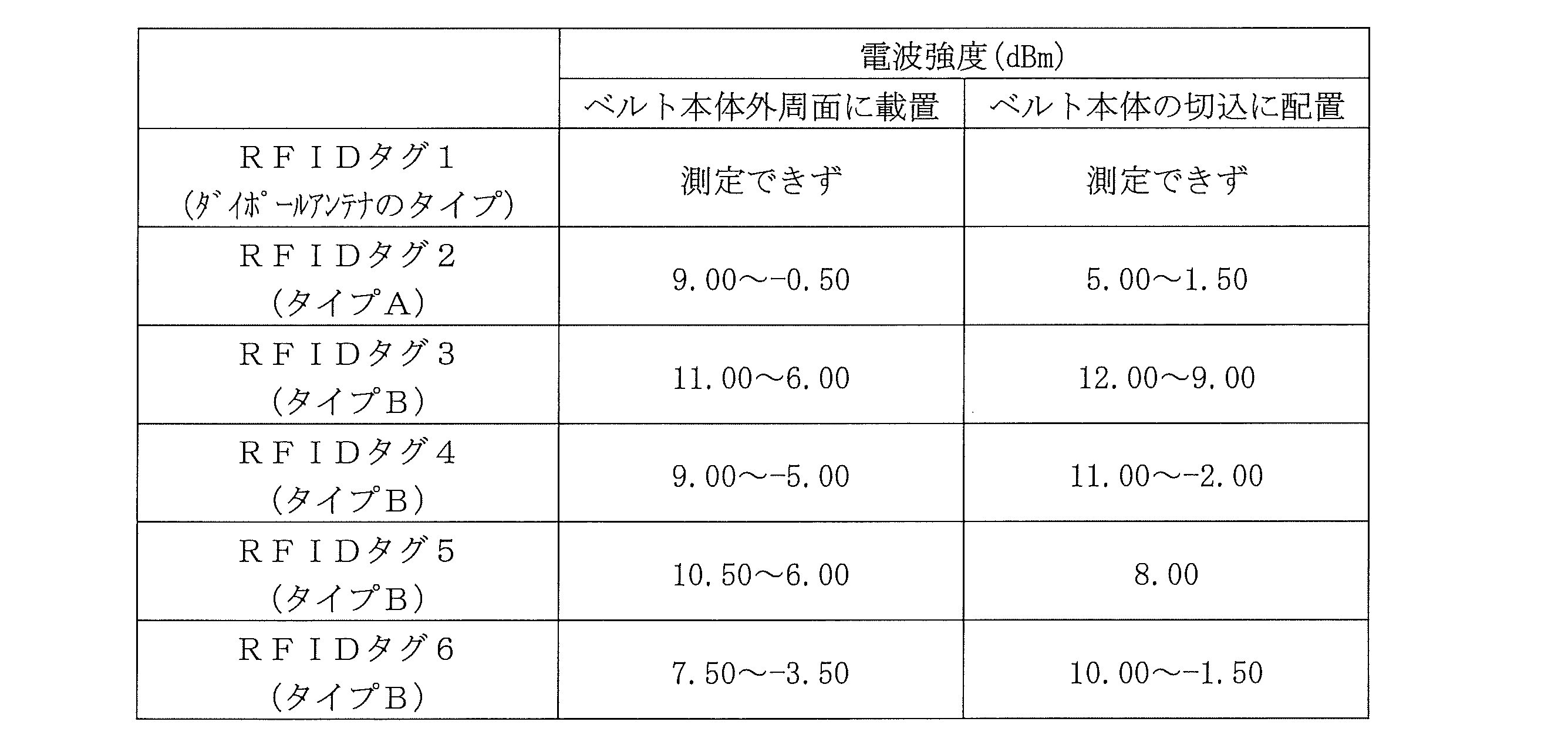
表1及び表2に示す結果から、本発明のベルトは、導電性の材料からなる芯体層を備える場合であっても、RFIDリーダライタとの通信が可能であることがわかる。なお、表2の電波強度は、値が低いほど通信性能が良好であることを示す指標である。
1:ベルト、10:ベルト本体、11:内側ゴム層、111:歯部、12:外側ゴム層、13:芯体層、131:心線、14:補強層、20:RFIDタグ、21:誘電体層、211:表面、212:裏面、22:放射素子、221:表面パターン、222:側面パターン、223:裏面パターン、224:第1領域、225:第2領域、226:スリット、23:ICチップ、24:接地導体、25:マイクロストリップライン、26:短絡線、27:給電線、28:金属層、29:ベース、2:プーリー、100:ベルト駆動システム
Claims (5)
- ベルト本体と、前記ベルト本体に設けられたRFIDタグとを備え、
前記ベルト本体は、導電性を示す材料で構成された芯体層を有し、
前記RFIDタグは、下記タイプA~CのいずれかのRFIDタグであり、
タイプA:誘電体層と、前記誘電体層の表面から裏面にかけてループ状に形成された放射素子と、前記放射素子に接続されたICチップとを備えるRFIDタグ
タイプB:誘電体層と、前記誘電体層の表面に形成された放射素子と、前記誘電体層の裏面に形成された接地導体と、前記放射素子に接続されたICチップとを備えるRFIDタグ
タイプC:誘電体層と、前記誘電体層の表面に形成された放射素子と、前記誘電体層の裏面に形成されて前記誘電体層の表面側からの電磁波を前記放射素子に向かって反射する金属層とを備えるRFIDタグ
そして、前記誘電体層の裏面が前記芯体層に対向するように前記RFIDタグが設けられている、ベルト。 - 前記芯体層が、炭素繊維で構成された芯体層である、請求項1に記載のベルト。
- 前記芯体層が、金属材料で構成された芯体層である、請求項1に記載のベルト。
- 前記RFIDタグが前記タイプBのRFIDタグである場合、
前記放射素子と、前記接地導体とを電気的に接続する2つの接続部が前記誘電体層に設けられており、
前記放射素子と前記2つの接続部と前記接地導体とが逆Fアンテナを構成している、請求項1に記載のベルト。 - 前記RFIDタグの交信周波数帯がUHF帯である、請求項1に記載のベルト。
Priority Applications (1)
| Application Number | Priority Date | Filing Date | Title |
|---|---|---|---|
| JP2023554059A JP7466070B1 (ja) | 2022-09-30 | 2023-08-16 | ベルト |
Applications Claiming Priority (2)
| Application Number | Priority Date | Filing Date | Title |
|---|---|---|---|
| JP2022-157371 | 2022-09-30 | ||
| JP2022157371 | 2022-09-30 |
Publications (1)
| Publication Number | Publication Date |
|---|---|
| WO2024070295A1 true WO2024070295A1 (ja) | 2024-04-04 |
Family
ID=90477251
Family Applications (1)
| Application Number | Title | Priority Date | Filing Date |
|---|---|---|---|
| PCT/JP2023/029584 Ceased WO2024070295A1 (ja) | 2022-09-30 | 2023-08-16 | ベルト |
Country Status (2)
| Country | Link |
|---|---|
| JP (1) | JP7466070B1 (ja) |
| WO (1) | WO2024070295A1 (ja) |
Citations (4)
| Publication number | Priority date | Publication date | Assignee | Title |
|---|---|---|---|---|
| JP2007094666A (ja) * | 2005-09-28 | 2007-04-12 | Nec Tokin Corp | 無線タグ |
| JP2010056683A (ja) * | 2008-08-26 | 2010-03-11 | Nitta Ind Corp | 無線icタグおよび無線通信システム |
| JP2011205384A (ja) * | 2010-03-25 | 2011-10-13 | Murata Mfg Co Ltd | アンテナ装置及び無線通信デバイス |
| JP2020118297A (ja) * | 2019-01-28 | 2020-08-06 | 三ツ星ベルト株式会社 | ベルト及びベルトの状態情報取得システム |
-
2023
- 2023-08-16 JP JP2023554059A patent/JP7466070B1/ja active Active
- 2023-08-16 WO PCT/JP2023/029584 patent/WO2024070295A1/ja not_active Ceased
Patent Citations (4)
| Publication number | Priority date | Publication date | Assignee | Title |
|---|---|---|---|---|
| JP2007094666A (ja) * | 2005-09-28 | 2007-04-12 | Nec Tokin Corp | 無線タグ |
| JP2010056683A (ja) * | 2008-08-26 | 2010-03-11 | Nitta Ind Corp | 無線icタグおよび無線通信システム |
| JP2011205384A (ja) * | 2010-03-25 | 2011-10-13 | Murata Mfg Co Ltd | アンテナ装置及び無線通信デバイス |
| JP2020118297A (ja) * | 2019-01-28 | 2020-08-06 | 三ツ星ベルト株式会社 | ベルト及びベルトの状態情報取得システム |
Also Published As
| Publication number | Publication date |
|---|---|
| JP7466070B1 (ja) | 2024-04-11 |
| JPWO2024070295A1 (ja) | 2024-04-04 |
Similar Documents
| Publication | Publication Date | Title |
|---|---|---|
| JP6741889B2 (ja) | ベルト及びベルトの状態情報取得システム | |
| JP7296535B1 (ja) | ベルト、ベルト駆動システム、及びベルトの製造方法 | |
| KR102758985B1 (ko) | Rfid 태그용 코일 | |
| US6836253B2 (en) | Transmitting and/or receiving unit for incorporation into an elastic structure | |
| US7151495B2 (en) | Transponder configuration, tire including a transponder, and method of producing a tire having a transponder | |
| KR101146161B1 (ko) | 무선 통신장치 및 방법 | |
| JP6751975B1 (ja) | Rfidタグ、rfidタグ内蔵タイヤ、およびrfidタグの製造方法 | |
| US20040041739A1 (en) | Wave antenna wireless communication device and method | |
| US12209636B2 (en) | Belt and system for acquiring belt state information | |
| US10268940B2 (en) | Stretchable broad impedance bandwidth RFID devices | |
| AU2022432013B2 (en) | Wear detection device and method for conveyor belt | |
| JP7466070B1 (ja) | ベルト | |
| US11984656B2 (en) | RF tag antenna, RF tag, tire provided with RF tag, and tire with built-in RF tag | |
| Shao et al. | Broadband and flexible textile RFID tags for tires | |
| JP2021037907A (ja) | Rfタグ付きタイヤ | |
| AU2022431126B2 (en) | Device and method for detecting longitudinal tear in conveyor belt | |
| JP7174415B2 (ja) | Rfidタグ、rfidタグ内蔵タイヤ、およびrfidタグの共振周波数を調整する方法 | |
| WO2023176331A1 (ja) | ベルト、ベルト駆動システム、及びベルトの製造方法 | |
| JP7818557B2 (ja) | ベルト及びベルトの状態情報取得システム | |
| JP2025122644A (ja) | ゴム製品用rfidタグ、ゴム製品、タイヤ及びゴム製品用rfidタグの製造方法 | |
| JPWO2020075732A1 (ja) | タイヤに埋め込まれるrfタグおよびrfタグ内蔵タイヤ | |
| JP2021056650A (ja) | 非接触型データ受送信体 | |
| EP4108478B1 (en) | AIRCRAFT TIRES | |
| JP2008153855A (ja) | ダイポールアンテナ | |
| KR20150052949A (ko) | 알에프아이디 태그 |
Legal Events
| Date | Code | Title | Description |
|---|---|---|---|
| ENP | Entry into the national phase |
Ref document number: 2023554059 Country of ref document: JP Kind code of ref document: A |
|
| 121 | Ep: the epo has been informed by wipo that ep was designated in this application |
Ref document number: 23871537 Country of ref document: EP Kind code of ref document: A1 |
|
| NENP | Non-entry into the national phase |
Ref country code: DE |
|
| 122 | Ep: pct application non-entry in european phase |
Ref document number: 23871537 Country of ref document: EP Kind code of ref document: A1 |