WO2024057367A1 - 固体レーザ装置および固体レーザ加工装置 - Google Patents
固体レーザ装置および固体レーザ加工装置 Download PDFInfo
- Publication number
- WO2024057367A1 WO2024057367A1 PCT/JP2022/034084 JP2022034084W WO2024057367A1 WO 2024057367 A1 WO2024057367 A1 WO 2024057367A1 JP 2022034084 W JP2022034084 W JP 2022034084W WO 2024057367 A1 WO2024057367 A1 WO 2024057367A1
- Authority
- WO
- WIPO (PCT)
- Prior art keywords
- solid
- light
- wavelength
- pulsed light
- generating element
- Prior art date
- Legal status (The legal status is an assumption and is not a legal conclusion. Google has not performed a legal analysis and makes no representation as to the accuracy of the status listed.)
- Ceased
Links
Images


Classifications
-
- H—ELECTRICITY
- H01—ELECTRIC ELEMENTS
- H01S—DEVICES USING THE PROCESS OF LIGHT AMPLIFICATION BY STIMULATED EMISSION OF RADIATION [LASER] TO AMPLIFY OR GENERATE LIGHT; DEVICES USING STIMULATED EMISSION OF ELECTROMAGNETIC RADIATION IN WAVE RANGES OTHER THAN OPTICAL
- H01S3/00—Lasers, i.e. devices using stimulated emission of electromagnetic radiation in the infrared, visible or ultraviolet wave range
- H01S3/30—Lasers, i.e. devices using stimulated emission of electromagnetic radiation in the infrared, visible or ultraviolet wave range using scattering effects, e.g. stimulated Brillouin or Raman effects
Definitions
- the present disclosure relates to a solid-state laser device that emits laser light used in laser processing, and a solid-state laser processing device.
- solid-state laser devices that output short pulse light have been widely used as laser light sources for microprocessing.
- Such solid-state laser devices often employ a MOPA (Master Oscillator Power Amplifier) method in which weak short pulse light output from a seed light source is amplified by a solid-state amplifier containing a solid-state active medium and output.
- MOPA Master Oscillator Power Amplifier
- the advantages of the MOPA system include the fact that it is easy to control the repetition frequency and that it is easy to obtain high output by increasing the number of solid-state amplifier stages.
- Patent Document 1 discloses that when temporarily stopping the output of pulsed light from the device, it is possible to avoid damage caused by excessive excitation of a solid-state amplifier, and also to avoid deterioration of beam propagation characteristics immediately after restarting the output.
- a laser light source device is disclosed.
- the laser light source device described in Patent Document 1 includes a fiber amplifier and a solid-state amplifier that amplify pulsed light output from a seed light source using a gain switching method, and a nonlinear optical element that converts the wavelength of the pulsed light output from the solid-state amplifier.
- an optical switch element that allows or blocks propagation of pulsed light from the fiber amplifier to the solid-state amplifier; and a control section that controls the seed light source and the optical switch element.
- the optical switch element is controlled by the control unit so that propagation of the pulsed light from the fiber amplifier to the solid-state amplifier is blocked during the output period of the pulsed light from the seed light source.
- an output stop state is realized in which the output of pulsed light is stopped from the nonlinear optical element without stopping the seed light source.
- the optical switch element is controlled by the control unit so that the propagation of light is allowed during a period different from the output period of the pulsed light from the seed light source.
- the emitted light noise propagates to the subsequent solid-state amplifier, and the energy of the active region of the solid-state amplifier in an excited state by the excitation light source is emitted.
- Patent Document 1 discloses a technique for preventing the generation of giant pulses, but when a giant pulse occurs, optical elements disposed downstream of the fiber amplifier and solid-state amplifier may be damaged or processing quality may be affected. It was difficult to suppress the decline. As described above, the technique described in Patent Document 1 has a problem in that damage to optical elements and the like due to the generation of unintended giant pulses in a solid-state laser device cannot be avoided.
- the present disclosure has been made in view of the above, and an object of the present disclosure is to obtain a solid-state laser device that can suppress damage to an optical element disposed after a solid-state active medium due to the generation of a giant pulse. do.
- a solid-state laser device includes a seed light source, a solid-state amplifier, a stimulated Raman scattering generating element, and a wavelength filter.
- the seed light source outputs pulsed light of a first wavelength.
- the solid-state amplifier has a solid-state active medium that outputs pulsed amplified light of a first wavelength, which is obtained by amplifying pulsed light.
- the stimulated Raman scattering generating element is placed after the solid-state amplifier, converts the pulsed amplified light into a second wavelength by stimulated Raman scattering with a wavelength conversion efficiency of 1% or more, and combines the first pulsed light of the first wavelength with the second pulsed light.
- the second pulsed light having the same wavelength is output.
- the wavelength filter uses the difference in wavelength to separate the second pulsed light from the optical path of the first pulsed light output from the stimulated Raman scattering generating element.
- the solid-state laser device has the effect of being able to suppress damage to optical elements disposed after the solid-state active medium due to the generation of giant pulses.
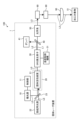
- FIG. 1 is a diagram showing a schematic example of a configuration of a solid-state laser processing apparatus including a solid-state laser device according to the first embodiment.
- the solid-state laser processing apparatus 100 includes a solid-state laser device 1, a deflector 80, and a condenser lens 90.
- the solid-state laser device 1 is an apparatus that emits laser light in the solid-state laser processing apparatus 100 using a solid active medium 21, which is a medium that causes stimulated emission, as described later.
- the solid-state laser processing apparatus 100 is an apparatus that processes a workpiece 51 using laser light emitted from the solid-state laser device 1 using the solid active medium 21. That is, in the solid-state laser processing apparatus 100, the laser light emitted from the solid-state laser device 1 is irradiated onto the workpiece 51 via the deflector 80 and the condenser lens 90, and is used to process the workpiece 51.
- the solid-state laser device 1 includes a seed light source 10, a control unit 11, a solid-state amplifier 20, an excitation light source 22, a dichroic mirror 23, and a stimulated Raman scattering (SRS) generating element 30. , a temperature control mechanism 31 , a wavelength filter 40 , a damper 41 , and an optical system 50 .
- SRS stimulated Raman scattering
- the seed light source 10 generates and outputs pulsed light LS of the first wavelength.
- the pulsed light LS of the first wavelength is a laser light that is amplified by the solid active medium 21 .
- the seed light source 10 is configured by, for example, a semiconductor laser, a fiber laser, or the like.
- the seed light source 10 may be a MOPA light source composed of the seed light source 10 and an amplifier (not shown).
- the control unit 11 controls various conditions such as the wavelength, pulse width, repetition frequency, and output of the pulsed light LS output from the seed light source 10.
- the solid-state amplifier 20 includes a solid-state active medium 21 that amplifies the pulsed light LS output from the seed light source 10 and outputs pulsed amplified light L0, which is the amplified pulsed light of the first wavelength.
- the type of solid active medium 21 is selected depending on the first wavelength, which is the wavelength of the pulsed light LS output from the seed light source 10. For example, when the first wavelength is 1064 nm, Nd:YVO 4 or Nd:YAG (Yttrium Aluminum Garnet) is preferably used as the solid active medium 21.
- the property of amplifying laser light by doping a solid base material such as YAG or YVO 4 with laser active ions such as Nd, Yb, or Tm and exciting it at a predetermined wavelength that is, gain
- the medium having the following is called a solid active medium 21.
- the solid-state amplifier 20 outputs the amplified pulse amplified light L0 of the first wavelength to the SRS generating element 30.
- the excitation light source 22 is a light source that outputs laser light LE that excites the solid active medium 21.
- the excitation light source 22 is composed of, for example, a semiconductor laser.
- the wavelength of the laser beam LE output from the excitation light source 22 is preferably 808 nm, or continuous light with wavelengths of 878.6 nm and 888 nm.
- the continuous light having a wavelength of 808 nm, 878.6 nm, or 888 nm output from the excitation light source 22 is also simply referred to as excitation light LE.
- the dichroic mirror 23 is provided to cause the pulsed light LS from the seed light source 10 and the excitation light LE from the excitation light source 22 to coaxially enter the solid active medium 21 .
- the dichroic mirror 23 is configured to reflect the pulsed light LS from the seed light source 10 and transmit the excitation light LE from the excitation light source 22.
- the SRS generating element 30 is arranged after the solid-state amplifier 20, and converts a part of the pulse amplified light L0 of the first wavelength amplified by the solid-state active medium 21 into the second pulse light L2 of the second wavelength by SRS, A first pulsed light L1 having a first wavelength and a second pulsed light L2 having a second wavelength are output.
- the second wavelength is longer than the first wavelength.
- the SRS generating element 30 wavelength-converts the pulse amplified light L0 to the second wavelength using SRS with a wavelength conversion efficiency of 1% or more.
- materials such as YVO 4 , GdVO 4 , Ba(NO 3 ) 2 , and diamond are used for the SRS generating element 30 .
- the SRS generating element 30 may be made of the above material as a base material to which laser active ions are added.
- the first wavelength is 1064 nm and the SRS generating element 30 is Nd:YVO 4 which is YVO 4 added with Nd as a laser active ion
- the second pulsed light L2 converted by the SRS generating element 30 is The wavelength is 1176 nm.
- the SRS generating element 30 includes an anti-reflection coating film that suppresses reflection of light of the first wavelength provided on an incident surface that is a surface on which the pulsed amplified light L0 is incident, and from which the first pulsed light L1 and the second pulsed light L2 are emitted.
- the light emitting device may include a non-reflective coating film provided on the output surface, which is a surface, for suppressing reflection of light of the first wavelength and the second wavelength.
- the non-reflection coating film provided on the incident surface can prevent the pulse amplified light L0 from returning to the seed light source 10, the excitation light source 22, and the solid active medium 21.
- the non-reflection coating film provided on the output surface can prevent the first pulsed light L1 and the second pulsed light L2 from returning to the seed light source 10, the excitation light source 22, and the solid active medium 21.
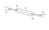
- FIG. 2 is a diagram schematically showing another example of the configuration of the SRS generating element.
- the SRS generating element 30 may be a non-coated structure in which no anti-reflection coating is provided on the incident surface 301 of the pulsed amplified light L0 and the exit surface 302 of the first pulsed light L1 and the second pulsed light L2. .
- the pulse amplified light L0 is incident on the incident surface 301 of the SRS generating element 30 at a Brewster angle ⁇ Bi
- the first pulsed light L1 and the second pulsed light L2 are incident on the incident surface 301 of the SRS generating element 30. It may be arranged so that the light is emitted at a Brewster angle ⁇ Bo with respect to the light emitting surface 302.
- an anti-reflection coating film is provided on the entrance/exit surface of a transmission type optical element.
- Anti-reflective coatings often have lower damage thresholds than the bulk or interface of optical elements.
- FIG. 2 when pulsed light is input to and output from the optical element at Brewster angles ⁇ Bi and ⁇ Bo, the reflectance at the input and output surfaces can be reduced even without an anti-reflection coating film. Therefore, damage to the anti-reflection coating film can be avoided, and damage to the optical element is less likely to occur.
- the temperature control mechanism 31 controls the temperature of the SRS generating element 30.
- the temperature control mechanism 31 includes a heating section that heats the SRS generating element 30 to a predetermined temperature, and a heating control section that controls heating by the heating section.
- the temperature control mechanism 31 controls the temperature of the SRS generating element 30 so that the wavelength conversion efficiency of the SRS generating element 30 is 1% or more, as will be described later.
- the wavelength filter 40 separates the second pulsed light L2 from the first pulsed light L1 and the second pulsed light L2 output from the SRS generation element 30 by utilizing the difference in wavelength. That is, the wavelength filter 40 separates the second pulsed light L2 from the optical path of the first pulsed light L1 output from the SRS generation element 30.
- the wavelength filter 40 transmits one of the first pulsed light L1 and the second pulsed light L2 emitted from the SRS generating element 30, and reflects the other.
- the first pulsed light L1 and the second pulsed light L2 which are lights of two wavelengths, are spatially separated.
- the wavelength filter 40 transmits the first pulsed light L1 and reflects the second pulsed light L2.
- the damper 41 is placed on the optical path of the second pulsed light L2 reflected by the wavelength filter 40.
- the damper 41 attenuates the second pulsed light L2.
- the damper 41 may be a measuring device such as a power meter.
- the optical system 50 is arranged on the optical path where the first pulsed light L1 passes through the wavelength filter 40.
- the first pulsed light L1 separated by the wavelength filter 40 passes through the optical system 50.
- the optical system 50 is configured with a lens or a mirror for transmitting the first pulsed light L1, but can be configured as appropriate depending on the use of the solid-state laser device 1 of the present disclosure.
- a solid state amplifier may be provided in the optical system 50.
- a nonlinear optical element for harmonic generation may be provided in the optical system 50. good.
- the third pulsed light L3, which is pulsed light that has been appropriately processed by the optical system 50, is output from the solid-state laser device 1.
- the deflector 80 deflects the third pulsed light L3 output from the solid-state laser device 1. Specifically, the deflector 80 arbitrarily displaces the irradiation position of the third pulsed light L3 on the workpiece 51. It is desirable that two deflectors 80 be provided so that the irradiation position of the third pulsed light L3 can be displaced on the workpiece 51 in two directions perpendicular to each other.
- An example of deflector 80 is a galvano scanner. Note that when the solid-state laser device 1 does not have the optical system 50, the deflector 80 deflects the pulsed light output from the wavelength filter 40.
- the condenser lens 90 condenses and irradiates the pulsed light deflected by the deflector 80, in the case of FIG. 1, the third pulsed light L3, onto an arbitrary position on the workpiece 51. As a result, the third pulsed light L3 is irradiated onto the workpiece 51, and laser processing is performed.
- FIG. 1 shows a case where the wavelength filter 40 transmits the first pulsed light L1 and reflects the second pulsed light L2, conversely, it reflects the first pulsed light L1 and reflects the second pulsed light L2. L2 may be transmitted.
- the damper 41 be placed on the transmission side of the wavelength filter 40 and the optical system 50 be placed on the reflection side of the wavelength filter 40.
- SRS is used for wavelength conversion of pulsed light.
- Wavelength conversion of pulsed light using SRS has advantages over harmonic generation, which is a common wavelength conversion method.
- harmonic generation the wavelength of the pulsed light incident on the nonlinear optical element is converted to 1/2 or less.
- the damage threshold of the bulk or coating film of an optical element becomes lower as the wavelength of the incident pulsed light becomes shorter. Therefore, when the wavelength of the giant pulse is converted by harmonic generation, there is a problem that optical elements such as the nonlinear optical element and the wavelength filter 40 are easily damaged by the shortened giant pulse.
- part of the pulsed light of the first wavelength is wavelength-converted into the pulsed light of the second wavelength, but the second wavelength is longer than the first wavelength. Therefore, the giant pulse whose wavelength has been converted to the second wavelength is less likely to damage optical elements such as the SRS generating element 30 and the wavelength filter 40 than the giant pulse having the first wavelength.
- nonlinear optical elements such as LBO (Lithium Triborate: LiB 3 O 5 ) and CLBO (Cesium Lithium Borate: CsLiB 6 O 10 ) used for harmonic generation have hygroscopic properties, humidity must be controlled.
- the SRS generating element 30 can be made of Nd:YVO 4 or the like used as a solid-state laser medium, there is no need for a special environment or treatment unlike in LBO, CLBO, etc. can be easily introduced into
- the wavelength conversion efficiency in the SRS generating element 30 it is preferable to set the wavelength conversion efficiency in the SRS generating element 30 to 1% or more.
- the intensity I SRS of the SRS light output from the SRS generating element 30 is given by the following equation (1).
- I SRS I Raman0 ⁇ exp(g Raman ⁇ I Pump ⁇ L) ...(1)
- I Raman0 is the intensity of the second wavelength pulsed light at the incident surface 301 of the SRS generating element 30
- g Raman is the Raman gain coefficient of the SRS generating element 30
- I Pump is the intensity of the second wavelength pulsed light at the incident surface 301 of the SRS generating element 30.
- the length L of the SRS generating element 30 is the length in the traveling direction of the pulsed light in the SRS generating element 30.
- the wavelength conversion efficiency ⁇ by SRS can be expressed by the following equation (2).
- the wavelength conversion efficiency ⁇ of SRS increases non-linearly with respect to the peak intensity of the first pulsed light L1.
- the wavelength conversion efficiency ⁇ increases. That is, the SRS generating element 30 functions as an attenuator for the first pulsed light L1 having a rated peak intensity or higher.
- the wavelength conversion efficiency ⁇ increases, so that the SRS generating element 30 generates a large amount of the second pulsed light L2 that is absorbed by the damper 41. This prevents the peak intensity of the first pulsed light L1 output from the SRS generating element 30 from becoming larger than necessary.
- the Raman gain coefficient at 893 cm -1 which has the largest Raman gain coefficient among the Raman modes of Nd:YVO 4 , is 4.5 cm/GW. It is preferable to set I Pump and L such that the value of I Pump ⁇ L is greater than or equal to "3 GW/cm" and less than or equal to "7 GW/cm.”
- the solid-state laser device 1 of the first embodiment preferably includes a temperature control mechanism 31 that controls the temperature of the SRS generating element 30.
- a wavelength conversion efficiency of 1% or more can be obtained for any I Pump ⁇ L.
- the wavelength conversion efficiency of SRS can be controlled, and the solid active medium by the giant pulse can be It is also possible to obtain the effect of avoiding damage to the SRS generating element 30 and the wavelength filter 40 which are arranged after the SRS generating element 21.
- I Pump and L may be set so that the wavelength conversion efficiency ⁇ is 1% or more, and the solid-state laser device 1 has the temperature control mechanism 31. You don't have to.
- the solid-state laser device 1 may be equipped with a temperature control mechanism 31 in order to change g Raman so that the wavelength conversion efficiency ⁇ becomes 1% or more. desirable.
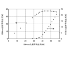
- FIG. 3 is a diagram showing an example of wavelength conversion characteristics to SRS when Nd:YVO 4 is used as the SRS generating element and pulsed light of 1064 nm is incident on the SRS generating element.
- the horizontal axis shows the 1064 nm input average output, which is the average input power of 1064 nm pulsed light
- the left vertical axis shows the 1064 nm output average output, which is the output average output of 1064 nm pulsed light
- the right vertical axis shows the SRS wavelength.
- 1176 nm output average output which is the output average output of a certain 1176 nm pulsed light, is shown.
- the beam diameter, pulse width, and repetition frequency of the incident pulsed light were kept constant, so the peak output and peak intensity at 1064 nm were proportional to the average output.
- SRS occurs when the average incident power of 1064 nm exceeds a certain value, and it can be confirmed that the average output power of 1064 nm is decreased and the average output power of 1176 nm is increased.
- the peak of the pulse amplified light L0 is preferably set so that the peak output of the first pulsed light L1 emitted from the SRS generating element 30 becomes maximum.
- the 1064 nm incident average output where the 1064 nm output average output is the maximum, when the 1064 nm incident average output changes by ⁇ 10%, the 1064 nm output average output changes by ⁇ 1% or less.
- the 1064 nm output average power on the left vertical axis is a constant value of about 36 W.
- the variation in the 1064 nm output average output with respect to the variation in the 1064 nm input average output is reduced, and this has the effect of increasing the stability of the output average output.
- the change in the average output in the experiment shown in Figure 3 means the change in the peak output, so a similar effect can be obtained by setting the 1064 nm incident peak output so that the 1064 nm output peak output is the maximum. can.
- the beam diameter of the pulsed light passing through the SRS generating element 30 and the wavelength filter 40 is large. If a giant pulse is generated in the configuration of the first embodiment, the SRS generating element 30 may be damaged by the giant pulse of the first wavelength. Furthermore, the SRS generating element 30 and the wavelength filter 40 may be damaged by the giant pulse whose wavelength is converted to the second wavelength.
- the damage threshold of an optical element caused by pulsed light depends on the peak intensity of the pulsed light. That is, the larger the beam diameter of the pulsed light that enters the optical element, the less likely it is to be damaged. On the other hand, the SRS threshold depends on the peak intensity of the pulsed light and the medium length.
- the desired SRS light can be generated by increasing the medium length of the SRS generation element 30. Is possible.
- a giant pulse occurs, it is possible to stably obtain the effect of avoiding damage to the SRS generating element 30 and the wavelength filter 40 disposed downstream of the solid active medium 21 due to the giant pulse.
- the pulse amplified light L0 is emitted from the solid active medium 21 in a converged state, and after the pulse amplified light L0 changes to a divergent state again behind the condensing point, the pulse amplified light L0 enters the SRS generating element 30.
- the SRS generating element 30 may be arranged as shown in FIG.
- the pulse amplified light L0 when the peak output of the pulse amplified light L0 is larger than the predetermined rated peak output, the pulse amplified light L0 is wavelength converted by the SRS generating element 30 and separated from the optical path by the wavelength filter 40. be done. As a result, damage to the optical element disposed downstream of the solid active medium 21 and deterioration in processing quality of the workpiece 51 due to the generation of the giant pulse are suppressed.
- the SRS generating element 30 may be made of the same material as the solid active medium 21, or the SRS generating element 30 may be made of a non-doped material or a lightly doped material of the same base material as the solid active medium 21. That is, the SRS generating element 30 transfers the same laser active ions as the laser active ions doped into the solid active medium 21 to the same base material as the solid active medium 21 . It may also be a lightly doped material doped at a concentration below . Alternatively, the SRS generating element 30 may be made of a non-doped material that is the same base material as the solid active medium 21 that does not contain laser active ions.
- the non-doped or lightly doped material is placed after the solid active medium 21.
- the non-doped material or the lightly doped material may be disposed downstream of the solid active medium 21 and separated from the solid active medium 21, or may be bonded to the surface of the solid active medium 21 from which the pulse amplified light L0 is emitted. may have been done.
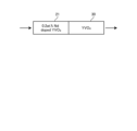
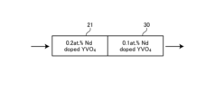
- FIGS. 4 to 6 are diagrams showing configuration examples of a solid active medium and an SRS generation element of a solid state laser device according to the second embodiment.
- the materials shown in FIGS. 4 to 6 can be used for the SRS generating element 30 when Nd:YVO 4 doped with Nd, which is a laser active ion, is used for the solid active medium 21.
- the SRS generating element 30 is made of the same material as the solid active medium 21 and has a doping concentration of 0.2 at. % Nd:YVO 4 is shown.
- FIG. 4 is a doping concentration of 0.2 at. % Nd:YVO 4 is shown.
- the SRS generating element 30 is made of non-doped YVO 4 which is the same base material as the base material of the solid active medium 21 and is not doped with laser active ions.
- the SRS generating element 30 injects Nd, which is the same as the laser active ion doped into the solid active medium 21, into YVO 4 , which is the same base material as the solid active medium 21.
- the case of a lightly doped material doped at a concentration less than or equal to the concentration of laser active ions of 21 is shown.
- the doping concentration is 0.1 at. % Nd:YVO 4 is used as the SRS generating element 30.
- the number or types of parts of the solid-state laser device 1 can be reduced. Furthermore, by bonding the SRS generating element 30 to the surface of the solid-state active medium 21 from which the pulse amplified light L0 is emitted, it is possible to downsize the solid-state laser device 1 including the solid-state active medium 21 and the SRS generating element 30. Become.
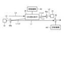
- FIG. 7 is a diagram schematically showing an example of the configuration of a solid-state laser device according to the third embodiment. Note that in the third embodiment, the configuration of the optical path between the solid active medium 21 and the wavelength filter 40 is different from that in the first embodiment, so FIG. It shows the configuration of the optical path.
- the solid-state laser device 1 includes folding mirrors 60a, 60b and a damper 61 between the solid-state active medium 21 and the wavelength filter 40 and after the SRS generating element 30. , a moving mechanism 62, a parallel plane substrate 63, and a rotating mechanism 64.
- the folding mirrors 60a and 60b When placed on the optical path along which the light travels, the folding mirrors 60a and 60b are placed between the SRS generating element 30 and the wavelength filter 40. In other words, the light passes through the SRS generating element 30, the folding mirrors 60a and 60b, and the wavelength filter 40 in this order. Further, in the arrangement on the optical path, at least one folding mirror 60a, 60b may be provided between the incident surface 301 of the SRS generating element 30 and the wavelength filter 40, and in the example of FIG. , 60b are shown. In the following, the folding mirrors 60a and 60b will be referred to as a folding mirror 60 unless they are distinguished from each other.
- the folding mirror 60 reflects the first pulsed light L1 of the first wavelength emitted from the SRS generating element 30 and transmits the second pulsed light L2 of the second wavelength.
- the folding mirror 60 is arranged so that the first pulsed light L1 of the first wavelength passes through the SRS generating element 30 at least twice.
- the position of the SRS generating element 30 is adjusted by a moving mechanism 62, which will be described later, so that the first pulsed light L1 passes through the SRS generating element 30 twice.
- FIG. 8 is a diagram schematically showing another example of the configuration of the solid-state laser device according to the third embodiment.
- FIG. 8 shows a state in which the position of the SRS generating element 30 is adjusted so that the first pulsed light L1, which is the light reflected by the folding mirror 60, all passes through the SRS generating element 30.
- the SRS generating element 30 is moved upward in the plane of the paper from the state shown in FIG. 8, the first pulsed light L1 reflected by the folding mirror 60b does not pass through the SRS generating element 30, as shown in FIG.
- the position where the first pulsed light L1 reflected by all the folding mirrors 60 passes through the SRS generating element 30 is called a reference position. Note that by appropriately setting the transmittance of the return mirror 60 for the second pulsed light L2, the partially reflected second pulsed light L2 is made incident on the SRS generation element 30, and the wavelength conversion efficiency in the SRS generation element 30 is increased to 1. % or more.
- the damper 61 attenuates the second pulsed light L2 transmitted by the folding mirror 60. Therefore, in the example of FIG. 7, the damper 61 is arranged on the transmission side of the folding mirror 60. Note that the damper 61 may be a measuring device such as a power meter.
- the moving mechanism 62 moves the SRS generating element 30. As shown in FIG. 8, when the SRS generating element 30 is located at the reference position by the moving mechanism 62, the SRS generating element 30 emits the first pulsed light L1 emitted from the solid active medium 21, the folding mirror 60a, It has a size that can transmit all of the first pulsed light L1 reflected by 60b. That is, at the reference position, the SRS generating element 30 is configured so that the first pulsed light L1 passes through the number of folding mirrors 60+1 times. The moving mechanism 62 moves the SRS generating element 30 so that the number of first pulsed lights L1 transmitted through the SRS generating element 30 can be changed from 1 to the number of folding mirrors 60 + 1.
- the SRS intensity depends on the length of the SRS generating element 30 and the peak intensity of the pulsed light of the first wavelength incident on the SRS generating element 30.
- the effective element length can be increased by making the pulsed light of the first wavelength, that is, the pulsed amplified light L0 and the first pulsed light L1, travel back and forth through the SRS generating element 30 a plurality of times.
- the second pulsed light L2 which is the SRS component of the second wavelength, is transmitted through the folding mirror 60 and excluded from the optical path of the first wavelength, I Raman in equation (1) is becomes essentially 0.
- the third embodiment has the effect of increasing the attenuation rate for the giant pulse compared to the case where the signal passes through the SRS generating element 30 having a long medium length once.
- the number of times the first pulsed light L1 passes through the SRS generating element 30 and the distance that the first pulsed light L1 passes through the SRS generating element 30 can be increased. It can also be changed.
- the moving mechanism 62 can move the SRS generating element 30 so that the beam diameter of the first pulsed light L1 incident on the SRS generating element 30 becomes larger.
- the diameter of the beam incident on the SRS generating element 30 can also be changed by changing the spread angle of the pulse amplified light L0 emitted from the solid active medium 21.
- the divergence angle of the pulsed light LS that is incident on the solid active medium 21 the diameter of the beam that is incident on the SRS generating element 30 is changed.
- the moving mechanism 62 has a beam diameter such that the first pulsed light L1 reflected by the folding mirror 60 is incident on the SRS generation element 30, and the first pulsed light L1 passes through the SRS generation element 30. At least one of the number of times the first pulsed light L1 passes through the SRS generating element 30 and the distance through which the first pulsed light L1 passes through the SRS generating element 30 are changed.
- the parallel plane substrate 63 is placed between the wavelength filter 40 and the folding mirror 60b placed before the wavelength filter 40.
- the parallel plane substrate 63 has a shape in which an entrance surface, which is a surface on which the first pulsed light L1 enters, and an exit surface, which is a surface from which the first pulsed light L1 is emitted, are parallel to each other.
- the rotation mechanism 64 changes the angle between the incident surface of the parallel plane substrate 63 and the optical axis of the first pulsed light L1 by rotating the parallel plane substrate 63.
- the rotation mechanism 64 rotates the parallel plane substrate 63 around two axes that are parallel to the incident surface of the parallel plane substrate 63 and orthogonal to each other.
- the rotation mechanism 64 corrects the optical axis shift caused by the first pulsed light L1 passing through the SRS generation element 30 by rotating the parallel plane substrate 63.
- the beam diameter of the first pulsed light L1 reflected by the folding mirror 60 is incident on the SRS generation element 30, the number of times the first pulsed light L1 passes through the SRS generation element 30, and the first pulsed light L1 includes a moving mechanism 62 that changes at least one of the distances through which the SRS generation element 30 passes.
- the moving mechanism 62 By moving the SRS generating element 30 with the moving mechanism 62, it is possible to change the number of times the first wavelength pulsed light passes through the SRS generating element 30 from 1 time to the number of folding mirrors 60 + 1 time. becomes. Furthermore, by changing the number of times the light passes through, it is possible to increase the substantial medium length of the SRS generating element 30.
- the possibility of damage to the optical element can be suppressed.
- the giant pulse when a giant pulse is generated can be reduced. This has the effect of increasing the attenuation rate of the pulse.
- a parallel plane substrate 63 that is a parallel flat plate and a rotation mechanism 64 that rotates the parallel plane substrate 63 are provided at a stage subsequent to the SRS generating element 30.
- the first pulsed light L1 passes through the SRS generation element 30 multiple times. By doing so, it becomes possible to correct the optical axis shift that occurs.
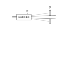
- FIG. 9 is a diagram schematically showing an example of the configuration of a solid-state laser device according to the fourth embodiment. Note that in the fourth embodiment, the configuration of the optical path between the solid active medium 21 and the wavelength filter 40 is different from that in the first embodiment, so FIG. It shows the configuration of the optical path.
- the solid-state laser device 1 further includes an aperture 70.
- the aperture 70 is disposed after the SRS generating element 30.
- the aperture 70 is a plate-shaped member in which an opening is formed.
- the aperture 70 is preferably a circular opening.
- the aperture 70 has a function of removing components of the pulsed light passing through the aperture 70, i.e., the first pulsed light L1 and the second pulsed light L2, whose divergence angle is greater than a set value, and transmitting components whose divergence angle is smaller than a set value.
- the SRS light of the second wavelength generated by a non-waveguide type bulk element has a component with a larger divergence angle than the pulsed light of the first wavelength. Therefore, by arranging the aperture 70 after the SRS generating element 30 as in the fourth embodiment, there is an effect that the pulse component of the second wavelength having a large divergence angle can be selectively removed.
- Solid-state laser device 10. Seed light source, 11. Control unit, 20. Solid-state amplifier, 21. Solid-state active medium, 22. Excitation light source, 23. Dichroic mirror, 30. SRS generation element, 31. Temperature control mechanism, 40. Wavelength filter, 41, 61. Damper. 50 Optical system, 51 Processing object, 60, 60a, 60b folding mirror, 62 Moving mechanism, 63 Parallel plane substrate, 64 Rotating mechanism, 70 Aperture, 80 Deflector, 90 Condensing lens, 100 Solid laser processing device, 301 Incident surface, 302 exit surface, L0 pulse amplified light, L1 first pulse light, L2 second pulse light, L3 third pulse light, LE excitation light, LS pulse light.
Landscapes
- Physics & Mathematics (AREA)
- Electromagnetism (AREA)
- Engineering & Computer Science (AREA)
- Plasma & Fusion (AREA)
- Optics & Photonics (AREA)
- Lasers (AREA)
- Optical Modulation, Optical Deflection, Nonlinear Optics, Optical Demodulation, Optical Logic Elements (AREA)
- Laser Beam Processing (AREA)
Priority Applications (3)
| Application Number | Priority Date | Filing Date | Title |
|---|---|---|---|
| PCT/JP2022/034084 WO2024057367A1 (ja) | 2022-09-12 | 2022-09-12 | 固体レーザ装置および固体レーザ加工装置 |
| JP2022574324A JP7254260B1 (ja) | 2022-09-12 | 2022-09-12 | 固体レーザ装置および固体レーザ加工装置 |
| TW112128990A TWI869957B (zh) | 2022-09-12 | 2023-08-02 | 固體雷射裝置以及固體雷射加工裝置 |
Applications Claiming Priority (1)
| Application Number | Priority Date | Filing Date | Title |
|---|---|---|---|
| PCT/JP2022/034084 WO2024057367A1 (ja) | 2022-09-12 | 2022-09-12 | 固体レーザ装置および固体レーザ加工装置 |
Publications (1)
| Publication Number | Publication Date |
|---|---|
| WO2024057367A1 true WO2024057367A1 (ja) | 2024-03-21 |
Family
ID=85795581
Family Applications (1)
| Application Number | Title | Priority Date | Filing Date |
|---|---|---|---|
| PCT/JP2022/034084 Ceased WO2024057367A1 (ja) | 2022-09-12 | 2022-09-12 | 固体レーザ装置および固体レーザ加工装置 |
Country Status (3)
| Country | Link |
|---|---|
| JP (1) | JP7254260B1 (https=) |
| TW (1) | TWI869957B (https=) |
| WO (1) | WO2024057367A1 (https=) |
Families Citing this family (1)
| Publication number | Priority date | Publication date | Assignee | Title |
|---|---|---|---|---|
| WO2025088680A1 (ja) * | 2023-10-24 | 2025-05-01 | 三菱電機株式会社 | レーザ装置およびレーザ加工装置 |
Citations (5)
| Publication number | Priority date | Publication date | Assignee | Title |
|---|---|---|---|---|
| JP2002031823A (ja) * | 2000-07-14 | 2002-01-31 | Japan Atom Energy Res Inst | 高出力短パルスレーザー光の発生システム |
| JP2003017787A (ja) * | 2001-07-04 | 2003-01-17 | Toshiba Corp | 固体レーザ装置及びqスイッチドライバの駆動回路 |
| JP2006019603A (ja) * | 2004-07-05 | 2006-01-19 | Matsushita Electric Ind Co Ltd | コヒーレント光源および光学装置 |
| US20060120418A1 (en) * | 2004-12-07 | 2006-06-08 | Imra America, Inc. | Yb: and Nd: mode-locked oscillators and fiber systems incorporated in solid-state short pulse laser systems |
| JP2008209909A (ja) * | 2007-01-31 | 2008-09-11 | Matsushita Electric Ind Co Ltd | 波長変換装置および2次元画像表示装置 |
Family Cites Families (3)
| Publication number | Priority date | Publication date | Assignee | Title |
|---|---|---|---|---|
| US7529281B2 (en) * | 2006-07-11 | 2009-05-05 | Mobius Photonics, Inc. | Light source with precisely controlled wavelength-converted average power |
| US20080261382A1 (en) * | 2007-04-19 | 2008-10-23 | Andrei Starodoumov | Wafer dicing using a fiber mopa |
| JP6456250B2 (ja) * | 2014-08-29 | 2019-01-23 | 三菱電機株式会社 | レーザ装置およびレーザ加工機 |
-
2022
- 2022-09-12 WO PCT/JP2022/034084 patent/WO2024057367A1/ja not_active Ceased
- 2022-09-12 JP JP2022574324A patent/JP7254260B1/ja active Active
-
2023
- 2023-08-02 TW TW112128990A patent/TWI869957B/zh active
Patent Citations (5)
| Publication number | Priority date | Publication date | Assignee | Title |
|---|---|---|---|---|
| JP2002031823A (ja) * | 2000-07-14 | 2002-01-31 | Japan Atom Energy Res Inst | 高出力短パルスレーザー光の発生システム |
| JP2003017787A (ja) * | 2001-07-04 | 2003-01-17 | Toshiba Corp | 固体レーザ装置及びqスイッチドライバの駆動回路 |
| JP2006019603A (ja) * | 2004-07-05 | 2006-01-19 | Matsushita Electric Ind Co Ltd | コヒーレント光源および光学装置 |
| US20060120418A1 (en) * | 2004-12-07 | 2006-06-08 | Imra America, Inc. | Yb: and Nd: mode-locked oscillators and fiber systems incorporated in solid-state short pulse laser systems |
| JP2008209909A (ja) * | 2007-01-31 | 2008-09-11 | Matsushita Electric Ind Co Ltd | 波長変換装置および2次元画像表示装置 |
Also Published As
| Publication number | Publication date |
|---|---|
| TWI869957B (zh) | 2025-01-11 |
| JPWO2024057367A1 (https=) | 2024-03-21 |
| JP7254260B1 (ja) | 2023-04-07 |
| TW202412416A (zh) | 2024-03-16 |
Similar Documents
| Publication | Publication Date | Title |
|---|---|---|
| US7885298B2 (en) | Method and apparatus for producing arbitrary pulsetrains from a harmonic fiber laser | |
| US9160136B1 (en) | External diffusion amplifier | |
| US9941654B2 (en) | Fiber-laser pumped crystal-laser | |
| US20140056321A1 (en) | Optical amplifier and process | |
| JP6295003B2 (ja) | 受動パルスシェイピング付き光源 | |
| JP5612964B2 (ja) | レーザ出射方法 | |
| US8873595B2 (en) | Laser processing method | |
| TWI869957B (zh) | 固體雷射裝置以及固體雷射加工裝置 | |
| US10256599B2 (en) | Laser light-source apparatus and laser pulse light generating method | |
| US10288981B2 (en) | Laser light-source apparatus and laser pulse light generating method | |
| WO2012099166A1 (ja) | レーザ装置 | |
| CN119072655A (zh) | 具有紫外线损伤减轻的激光频率转换 | |
| TWI897602B (zh) | 雷射裝置及雷射加工裝置 | |
| FI125097B (fi) | Tehokas pulssitettu itseherätteinen CO2-laser | |
| JP7214056B1 (ja) | レーザ装置およびレーザ加工機 | |
| JP7500069B2 (ja) | 光発振器 | |
| US8457171B2 (en) | Miniaturized laser amplifier arrangement having a pump source | |
| Büker et al. | High-pulse-energy Q-switched Ho3+: YAG laser | |
| JP2025521256A (ja) | 光同期マルチステージ/マルチパス増幅を有する受動高エネルギーqスイッチレーザーシステム | |
| Zimer et al. | High-power Nd: YAG-MISER |
Legal Events
| Date | Code | Title | Description |
|---|---|---|---|
| ENP | Entry into the national phase |
Ref document number: 2022574324 Country of ref document: JP Kind code of ref document: A |
|
| 121 | Ep: the epo has been informed by wipo that ep was designated in this application |
Ref document number: 22958702 Country of ref document: EP Kind code of ref document: A1 |
|
| NENP | Non-entry into the national phase |
Ref country code: DE |
|
| 122 | Ep: pct application non-entry in european phase |
Ref document number: 22958702 Country of ref document: EP Kind code of ref document: A1 |