WO2024053724A1 - Signal processing device, signal processing method, and program - Google Patents
Signal processing device, signal processing method, and program Download PDFInfo
- Publication number
- WO2024053724A1 WO2024053724A1 PCT/JP2023/032792 JP2023032792W WO2024053724A1 WO 2024053724 A1 WO2024053724 A1 WO 2024053724A1 JP 2023032792 W JP2023032792 W JP 2023032792W WO 2024053724 A1 WO2024053724 A1 WO 2024053724A1
- Authority
- WO
- WIPO (PCT)
- Prior art keywords
- phase noise
- signal
- measurement target
- zero
- signal processing
- Prior art date
Links
- 238000012545 processing Methods 0.000 title claims abstract description 45
- 238000003672 processing method Methods 0.000 title claims description 5
- 238000005259 measurement Methods 0.000 claims abstract description 92
- 238000004364 calculation method Methods 0.000 claims abstract description 27
- 238000009795 derivation Methods 0.000 claims abstract description 18
- 238000006243 chemical reaction Methods 0.000 claims abstract description 8
- 238000012360 testing method Methods 0.000 abstract description 7
- 238000001228 spectrum Methods 0.000 description 19
- 238000000034 method Methods 0.000 description 17
- 238000010586 diagram Methods 0.000 description 12
- 239000013078 crystal Substances 0.000 description 8
- 238000004891 communication Methods 0.000 description 5
- 238000011156 evaluation Methods 0.000 description 4
- 238000004458 analytical method Methods 0.000 description 3
- 239000006185 dispersion Substances 0.000 description 3
- 230000009977 dual effect Effects 0.000 description 3
- 230000000737 periodic effect Effects 0.000 description 3
- 239000002131 composite material Substances 0.000 description 2
- 229920005994 diacetyl cellulose Polymers 0.000 description 1
- 230000014509 gene expression Effects 0.000 description 1
- 239000000463 material Substances 0.000 description 1
- 239000000203 mixture Substances 0.000 description 1
- 230000005236 sound signal Effects 0.000 description 1
- 230000003595 spectral effect Effects 0.000 description 1
- 230000007704 transition Effects 0.000 description 1
Images


Classifications
-
- G—PHYSICS
- G01—MEASURING; TESTING
- G01R—MEASURING ELECTRIC VARIABLES; MEASURING MAGNETIC VARIABLES
- G01R19/00—Arrangements for measuring currents or voltages or for indicating presence or sign thereof
- G01R19/06—Measuring real component; Measuring reactive component
-
- G—PHYSICS
- G01—MEASURING; TESTING
- G01R—MEASURING ELECTRIC VARIABLES; MEASURING MAGNETIC VARIABLES
- G01R19/00—Arrangements for measuring currents or voltages or for indicating presence or sign thereof
- G01R19/175—Indicating the instants of passage of current or voltage through a given value, e.g. passage through zero
-
- G—PHYSICS
- G01—MEASURING; TESTING
- G01R—MEASURING ELECTRIC VARIABLES; MEASURING MAGNETIC VARIABLES
- G01R23/00—Arrangements for measuring frequencies; Arrangements for analysing frequency spectra
- G01R23/16—Spectrum analysis; Fourier analysis
Definitions
- the present invention relates to a signal processing device, a signal processing method, and a program.
- phase noise has been known as one of the evaluation indicators of the performance (e.g. frequency stability) of devices to be measured such as crystal oscillators, audio equipment, digital equipment, communication equipment, etc.
- Various methods of measurement are being considered.
- the signal to be measured output from the device under test is measured using two independent measuring instruments, and each of the two measuring instruments is A cross-correlation spectrum method is known in which the phase noise of the DUT is measured by removing the phase noise of each of the two measuring instruments by taking the cross-correlation spectrum of the measurement signal of the DUT (for example, Patent Document 1). Note that the cross-correlation spectrum is also called a cross spectrum.
- one of the objects of the present disclosure is to provide a signal processing device, a signal processing method, and a program that can measure the phase noise of a device to be measured while reducing at least one of measurement cost and measurement time.
- a signal processing device includes an acquisition unit that acquires a plurality of measurement target signals obtained by independently analog-to-digital conversion of a measurement target signal output from a measurement target device by a plurality of measuring instruments; a derivation unit that derives a plurality of zero-crossing fluctuations (ZCF), which are time differences between the zero-crossing time of each measurement target signal and the zero-crossing time of an ideal sine wave signal; A calculation unit that calculates phase noise of the device to be measured.
- ZCF zero-crossing fluctuations
- a signal processing device acquires a plurality of measurement target signals output from a measurement target device and each independently analog-to-digital converted by a plurality of measuring instruments, Deriving a plurality of zero-crossing fluctuations (ZCFs), which are time differences between the zero-crossing times of each of the plurality of measurement target signals and the zero-crossing time of an ideal sine wave signal, and based on the plurality of ZCFs, performing the measurement. Calculate the phase noise of the target device.
- ZCFs zero-crossing fluctuations
- a program includes an acquisition unit that causes a computer to acquire a plurality of measurement target signals outputted from a measurement target device and independently analog-to-digital converted by a plurality of measurement devices; a derivation unit that derives a plurality of zero-crossing fluctuations (ZCFs), which are time differences between the zero-crossing times of each of the plurality of measurement target signals and the zero-crossing time of an ideal sine wave signal; and based on the plurality of ZCFs, It functions as a calculation unit that calculates the phase noise of the device to be measured.
- ZCFs zero-crossing fluctuations
- phase noise of a device it is possible to measure the phase noise of a device to be measured while reducing at least one of measurement cost and measurement time.
- FIG. 1 is a diagram showing an example of the configuration of a measurement system according to the present embodiment.
- 1 is a diagram illustrating an example of the configuration of a signal processing device according to an embodiment.
- FIG. 3 is a diagram showing an example of zero-crossing time of a signal to be measured according to the present embodiment. It is a figure showing an example of ZCF concerning this embodiment. It is a figure showing an example of setting for ZCF derivation concerning this embodiment. It is a figure showing other examples of settings for ZCF derivation concerning this embodiment. It is a flowchart which shows an example of operation of the measurement system concerning this embodiment.
- FIG. 1 is a diagram showing an example of the configuration of a measurement system according to the present embodiment.
- 1 is a diagram illustrating an example of the configuration of a signal processing device according to an embodiment.
- FIG. 3 is a diagram showing an example of zero-crossing time of a signal to be measured according to the present embodiment. It is a figure showing an example of ZCF concerning this embodiment. It
- 3 is a diagram illustrating an example of a comparison between phase noise measured by the signal processing device 50 according to the present embodiment and phase noise measured using a cross-correlation spectrum method.
- 1 is a diagram illustrating an example of generalization of the configuration of a measurement system according to the present embodiment.
- the measurement system includes a device to be measured (hereinafter referred to as "DUT: Device Under Test”), a divider that distributes a signal to be measured output from the DUT, and a divider connected to the divider. It includes a plurality of measuring instruments and a signal processing device connected to the plurality of measuring instruments.
- DUT Device Under Test
- N the number of multiple measuring devices
- N the number of multiple measuring devices
- FIG. 1 is a diagram showing an example of the configuration of a measurement system according to the present embodiment.
- N 2
- the measurement system 1 includes a DUT 10, a distributor 20, two independent analog-to-digital converters (ADCs) 30a and 30b, and an ADC 30a. and 30b, and a signal processing device 50.
- ADCs analog-to-digital converters
- the measuring device MDa includes an ADC 30a and a clock circuit 40a
- the measuring device MDb includes an ADC 30b and a clock circuit 40b.
- the measuring devices MDa and b are not distinguished, they will simply be collectively referred to as measuring devices MD.
- the ADCs 30a and 30b are not distinguished, they are collectively referred to as the ADC 30, and when the clock circuits 40a and 40b are not distinguished, they are collectively referred to as the clock circuit 40.
- FIG. 1 is merely an example, and some configurations may be omitted, configurations not shown may be added, or the arrangement of some configurations may be changed.
- a plurality of measuring devices MD may be connected in parallel without providing the distributor 20.
- the DUT 10 is an oscillator that outputs a periodic signal such as a sine wave or a rectangular wave as a signal to be measured.
- the DUT 10 includes, for example, a crystal oscillator, a voltage controlled oscillator (VCO), a temperature compensated crystal oscillator (TCXO), and an oven controlled crystal oscillator (OCXO). ), audio equipment such as audio players and music players with earphone output terminals, communication equipment such as wireless communication terminals or base stations, arbitrary waveform generators with BNC (Bayonet Neill Concelman) output terminals, etc. be.
- VCO voltage controlled oscillator
- TXO temperature compensated crystal oscillator
- OXO oven controlled crystal oscillator
- the distributor 20 is, for example, a power splitter, and distributes the measurement target signal output from the DUT 10 and outputs the distributed measurement target signal to each ADC 30.
- Each ADC 30 measures the measurement target signal output from the distributor 20. Specifically, each ADC 30 samples the measurement target signal output from the distributor 20 based on the clock signal output from the corresponding clock circuit 40, and converts it from an analog signal to a digital signal (discrete data). You may.
- Each clock circuit 40 generates a clock signal and outputs the generated clock signal to the corresponding ADC 30.
- Each clock circuit 40 may be, for example, an oscillator such as a crystal oscillator, a VCO, a TCXO, or an OCXO.
- the clock signal may be a periodic signal with a predetermined frequency (eg, 27 MHz).
- a clock signal is also called a reference signal or a local signal.
- Each measuring device MD including the ADC 30 and the clock circuit 40 may be, for example, an audio device such as an audio recorder, or a communication device such as a base station or a wireless communication terminal. Note that each measuring device MD does not need to include the clock circuit 40, but may include at least the ADC 30.
- the measurement of the measurement target signal in each measuring device MD may include conversion from an analog signal to a digital signal by the ADC 30.
- the signal processing device 50 calculates the phase noise of the DUT 10 based on the measurement target signal output from each measuring device MD.
- the signal processing device 50 is composed of a device including at least a processor.
- phase noise is a variation in phase or frequency of a signal to be measured.
- jitter is a fluctuation in a signal waveform in the time direction.
- the phase noise calculated by the signal processing device 50 may include at least one of PI (Phase independent) noise, jitter, and amplitude modulation (AM).
- FIG. 2 is a diagram showing an example of the configuration of the signal processing device 50 according to the present embodiment.
- the signal processing device 50 includes an acquisition section 501, a derivation section 502, and a calculation section 503.
- the configuration of the signal processing device 50 is realized by, for example, at least one of a processor and a program executed by the processor.
- the acquisition unit 501 acquires a plurality of measurement target signals respectively output from a plurality of measuring devices MD. For example, in FIG. 1, the acquisition unit 501 acquires two measurement target signals output from measuring instruments MDa and MDb, respectively.
- the derivation unit 502 calculates a plurality of zero-crossing fluctuations, which are time differences between the zero-crossing time of each of the plurality of measurement target signals acquired by the acquisition unit 501 and the zero-crossing time of an ideal sine wave signal.
- ZCF Zero-Crossing Fluctuations
- the derivation of the plurality of ZCFs is also called zero-crossing analysis (ZCA). Since ZCA is a type of time domain analysis (TDA), it is useful for measuring jitter, which is impossible with frequency domain analysis (FDA).
- TDA time domain analysis
- FDA frequency domain analysis
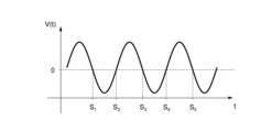
- FIG. 3 is a diagram illustrating an example of the zero crossing time of the signal to be measured according to the present embodiment.
- the horizontal axis is time t
- the vertical axis is voltage V
- voltage V(t) of the signal to be measured at time t is shown.
- k is the zero-crossing time index
- M is the number of zero-crossing times.
- the zero crossing time may also be referred to as a zero crossing point (ZCP).
- the intervals between the zero crossing times sk of the signal to be measured are not equal due to the influence of noise of the DUT 10 and each measuring device MD.
- the zero crossing times s ' k (not shown) of the ideal sine wave signal are equally spaced.
- the ideal zero-crossing time of a sine wave signal is expressed, for example, by the function s'(k) of Equation 1 below.
- f'c is the frequency of an ideal sine wave signal (for example, the average frequency of period T).
- the zero crossing time s'k of the index k of the ideal sine wave signal can be set to the value of the function s'(k) shown in Equation 1.
- FIG. 4 is a diagram showing an example of the ZCF according to this embodiment.
- the horizontal axis is the index k of the zero crossing time
- the vertical axis is the time t
- the zero-crossing time function s'(k) of an ideal sinusoidal signal is the zero-crossing time function s'(k) of an ideal sinusoidal signal.
- FIG. 5 is a diagram illustrating an example of setup for ZCF derivation according to the present embodiment.
- an audio player is used as the DUT 10
- a first audio recorder is used as the measuring device MDa including the ADC 30a and the clock circuit 40b
- a second audio recorder is used as the measuring device MDb including the ADC 30b and the clock circuit 40b. shall be taken as a thing.
- the measurement target signal output from the DUT 10 is a playback signal c(t) of the audio player.
- the reproduced signal c(t) may be, for example, a signal in a relatively low frequency region such as 12 kHz (hereinafter referred to as a "low frequency signal").
- the formula shown below is of course applicable not only to the audio player and the first and second audio recorders, but also to any DUT 10 and measuring device MD.
- the audio player as DUT 10 includes a digital-to-analog converter (DAC) and a clock circuit.
- the audio player is configured as a dual channel player including two single channel players corresponding to the left channel and right channel respectively, two DACs and two low pass players corresponding to the left channel and right channel respectively. It may also include a filter (LPF: Low Pass Filter).
- LPF Low Pass Filter
- a playback waveform v[i] corresponding to each of the left channel and right channel is converted into an analog signal by a DAC, and the jitter n jitter and amplitude from the clock circuit are converted into the analog signal via the LPF.
- Amplitude Modulation A reproduced signal c(t) which is the sum of n AM and PI noise n PI is generated and output.
- the first audio recorder as the measuring device MDa includes an ADC 30a and a clock circuit 40a.
- the first audio recorder is configured as a dual channel recorder (pseudo single channel recorder) including two single channel recorders corresponding to the left channel and right channel, respectively. It may also include two corresponding ADCs 30a and two LPFs.
- an analog signal obtained by adding jitter a jitter from the clock circuit 40a, amplitude a AM , and PI noise a PI to the playback signal c(t) output from the audio player passes through an LPF. , converted into a digital signal x[i] by the ADC 30a and output. Note that i is the index of the signal recorded by the first audio recorder.
- the second audio recorder as measuring device MDb includes an ADC 30b and a clock circuit 40b.
- the second audio recorder is configured as a dual channel recorder (pseudo single channel recorder) including two single channel recorders corresponding to the left channel and right channel, respectively. It may also include two corresponding ADCs 30b and two LPFs.
- an analog signal obtained by adding jitter b jitter from the clock circuit 40b, amplitude b AM , and PI noise b PI to the playback signal c(t) output from the audio player is passed through an LPF. , and is converted into a digital signal y[i] by the ADC 30b and output. Note that i is the index of the signal recorded by the second audio recorder.
- the derivation unit 502 calculates the time difference between the zero crossing time s k of the measurement target signal x[i] outputted from the first audio recorder as the measuring device MDa and the zero crossing time s' k of the ideal sine wave signal. Perform ZCA to derive a certain ZCF ⁇ s k .
- k is the zero-crossing time index
- ⁇ is the angular frequency
- a 0 is the amplitude
- n jitter (s' k ) is the jitter of index k added by the audio player as DUT 10
- n PI ( s' k ) is the PI noise of index k added by the audio player
- a PI (s' k ) is the PI noise of index k added by the first audio recorder as the measuring device MDa
- a jitter (s ' k ) is the jitter of index k added by the first audio recorder.
- the derivation unit 502 calculates the difference between the zero crossing time r k of the measurement target signal y[i] output from the second audio recorder as the measuring device MDb and the zero crossing time r ' k of the ideal sine wave signal.
- ZCA is performed to derive the time difference ZCF ⁇ rk .
- k, ⁇ , A 0 , n jitter (s' k ), and n PI (s' k ) are as explained in Equation 3.
- b PI (s' k ) is the PI noise of index k added by the second audio recorder as the measuring device MDb
- b jitter (s' k ) is the jitter of index k added by the first audio recorder. It is. Since the first and second audio recorders simultaneously sample the playback signal c(t) output from the audio player, the ideal sine wave signal zero-crossing time s' k of the first and second audio recorders and r'k are the same. Therefore, the deriving unit 502 can replace r ' k in Equation 4 with s ' k to obtain Equation 5.
- the reproduction signal c(t) corresponding to the left channel is input to the first and second audio recorders as measuring devices MDa and MDb, respectively, but the invention is not limited to this.
- a composite signal c(t) of reproduction signals corresponding to the left channel and the right channel may be input to the first and second audio recorders, respectively.
- the derivation unit 502 derives a plurality of ZCFs corresponding to each of the plurality of measuring devices MD (for example, the first and second audio recorders in FIG. 5).
- the calculation unit 503 calculates the phase noise of the DUT 10 based on the plurality of ZCFs derived by the derivation unit 502.
- the calculation unit 503 may calculate the phase noise of the DUT 10 based on the difference between the first ZCF and the second ZCF of the plurality of ZCFs. Further, the calculation unit 503 may calculate the phase noise of the DUT 10 based on the sum of the first ZCF and the second ZCF of the plurality of ZCFs. Further, the calculation unit 503 may calculate the phase noise of each of the measuring devices MDa and MDb as well as the phase noise of the DUT 10.
- a first ZCF ( ⁇ s k ) corresponding to the first audio recorder as the measuring device MDa and a second ZCF ( ⁇ r k ) is derived by ZCA
- the calculation unit 503 calculates the first ZCF ( ⁇ s k ), the second ZCF ( ⁇ r k ), the difference between the first and second ZCFs ( ⁇ s k ⁇ r k ), Based on the sum of the first and second ZCFs ( ⁇ s k + ⁇ r k ), the phase noise ( ⁇ n2 ) of the DUT 10, the phase noise ( ⁇ a2 ) of the measuring device MDa, and the phase noise ( ⁇ b2 ) of the measuring device MDb are calculated. It may be calculated.
- the four parameters i.e., ⁇ s k , ⁇ r k , ⁇ s k ⁇ r k , ⁇ s k + ⁇ r k
- ⁇ n2 is the root mean square (RMS) of the ZCF of the audio player as the DUT 10
- ⁇ a2 is the RMS of the ZCF of the first audio recorder as the measuring device MDa
- ⁇ b2 is the RMS of the ZCF of the second audio recorder as measuring device MDb.
- V ⁇ indicates dispersion.
- ⁇ n2 , ⁇ a2 and ⁇ b2 can also be considered as phase noise of the audio player and the first and second audio recorders.
- the calculation unit 503 can evaluate the phase noise of the audio player as the DUT 10 by distinguishing it from the phase noise of the first and second audio recorders as the measuring devices MDa and MDb.
- the phase noises ⁇ n2 , ⁇ a2 and ⁇ b2 may be calculated based on Equations 6 to 8 without using Equation 9.
- Equations 10 to 12 below are relational expressions based on the model.
- ⁇ n2 , ⁇ a2 , and ⁇ b2 can also be said to be the phase noise of the audio player and the first and second audio recorders, as explained in Equations 6 to 9.
- k, ⁇ , and A 0 are as explained in Equation 3.
- j (s' k ) indicates the jitter (n jitter (s' k )) input to the audio player as the DUT 10
- n PI (s' k ) indicates the PI noise (n PI ( s'k )).
- V ⁇ indicates dispersion.
- a jitter (s' k ) indicates the jitter input to the first audio recorder as the measuring device MDa
- a PI (s' k ) is the PI noise added by the first audio recorder.
- b jitter (s' k ) indicates the jitter input to the second audio recorder as the measuring device MDb
- b PI (s' k ) is the PI noise added by the second audio recorder.
- the calculation unit 503 may be separated from the phase noise of the audio player.
- the phase noise ⁇ n3 of the audio player may be expressed by Equation 13 below.
- the calculation unit 503 may calculate the jitter j (s' k ) of the audio player as the DUT 10 based on Equations 10 and 13 above.
- the jitter may be expressed by Equation 14.
- dev ⁇ indicates the standard deviation.
- j (s' k ) is as explained in Equation 10
- ⁇ n3 is the phase noise of the audio player as DUT 10 in the configuration shown in FIG. 6
- ⁇ n2 is the phase noise of the audio player as DUT 10 in the configuration shown in FIG. is the phase noise of
- FIG. 7 is a flowchart showing an example of the operation of the measurement system according to this embodiment. Note that the steps shown in FIG. 7 are only an example, and some steps (for example, step S107) may not be performed, or steps not shown may be added.
- step 101 the DUT 10 outputs the signal to be measured.
- the measurement target signal output from the DUT 10 includes phase noise in the DUT 10.
- step S102 the distributor 20 distributes the measurement target signal output from the DUT 10 into N signals.
- N (N ⁇ 2) measurement devices MD independently convert the N measurement target signals distributed by the distributor 20 from analog signals to digital signals and output the converted signals.
- N 2
- the measuring device MDa converts the signal to be measured from the distributor 20 from an analog signal to a digital signal using the ADC 30a, based on the clock signal from the clock circuit 40a, and outputs the converted signal.
- the measuring device MDb converts the signal to be measured from the distributor 20 from an analog signal to a digital signal using the ADC 30b, based on the clock signal from the clock circuit 40b, and outputs the converted signal.
- step S104 the signal processing device 50 acquires N measurement target signals respectively output from the N measurement devices MD.
- Each signal to be measured includes phase noise in the DUT 10 and phase noise in each measuring device.
- the signal processing device 50 acquires the measurement target signal output from the measuring device MDa and the measuring target signal from the measuring device MDb.
- step S105 the signal processing device 50 derives N ZCFs, which are the time differences between the zero-crossing time of each of the N measurement target signals acquired in step S104 and the zero-crossing time of an ideal sine wave signal. do.
- the signal processing device 50 uses an index of the zero-crossing time of the measurement target signal x[i] output from the first audio recorder as the measuring device MDa and the zero-crossing time of the ideal sine wave signal.
- ZCF ⁇ s k which is the time difference of k, is derived.
- the signal processing device 50 calculates the time difference of index k between the zero crossing time of the signal to be measured y[i] output from the second audio recorder as the measuring device MDb and the zero crossing time of the ideal sine wave signal.
- a certain ZCF ⁇ rk is derived.
- the signal processing device 50 may measure the phase noise of the N measurement devices MD as well as the phase noise of the DUT 10 based on the N ZCFs derived in step S105. For example, in the configuration shown in FIG. 5, the signal processing device 50 calculates ZCF ⁇ s k of the first audio recorder as the measuring device MDa, ZCF ⁇ r k of the second audio recorder as the measuring device MDb, and ZCF ⁇ s k and ZCF ⁇ r k Based on the difference between them, the phase noise ⁇ a2 of the measuring device MDa and the phase noise ⁇ b2 of the measuring device MDb are calculated together with the phase noise ⁇ n2 of the DUT 10. Further, the signal processing device 50 may verify the calculated phase noises ⁇ n2 , ⁇ a2 and ⁇ b2 based on the sum of ZCF ⁇ s k and ZCF ⁇ rk .
- step S107 the signal processing device 50 calculates the phase noise of the N measurement devices MD calculated in step S106, but evaluates only the phase noise of the DUT 10. Therefore, the phase noise of the N measuring devices MD can be removed analytically, rather than being removed due to the uncorrelation of the signals to be measured from the N measuring devices MD as in the cross-correlation spectrum method.
- the signal processing device 50 processes N measurement target signals (for example, in FIG. 5, x[i] and y[i]), it is possible to calculate not only the phase noise ⁇ n2 of the DUT 10 but also the phase noise of the N measurement devices MD (for example, in FIG. 5, the phase noises ⁇ n2 , ⁇ a2 and ⁇ b2 ). Only the phase noise of DUT 10 can be evaluated. Therefore, the phase noise of the DUT 10 can be measured with high precision even if an inexpensive measuring device MD that does not necessarily have low noise is used.
- the signal processing device 50 detects not only the phase noise of the DUT 10 but also the phase noise of the N measuring devices MD (for example, in FIG. 5, the phase noise Since only the phase noise of the DUT 10 can be evaluated by calculating ⁇ n2 , ⁇ a2 , and ⁇ b2 ), the phase noise of the DUT 10 can be measured with high precision without increasing the measurement time unlike the cross-correlation spectrum method.
- the signal to be measured is a low frequency signal (for example, a 12 kHz sine wave signal)
- the signal to be measured is a signal in a relatively high frequency domain (hereinafter referred to as "high frequency signal", for example, a 27 MHz sine wave signal)
- high frequency signal for example, a 27 MHz sine wave signal
- down conversion can be applied to the high frequency signal, so conventional The cross-correlation spectrum method can be applied. Therefore, the phase noise measured by the signal processing device 50 and the phase noise measured using the conventional cross-correlation spectrum method will be compared and evaluated.
- the high frequency signal is not limited to, for example, the above-mentioned 27 MHz, but may be a frequency signal of several MHz to several tens of GHz, etc.
- FIG. 8 is a diagram showing an example of a comparison between the phase noise measured by the signal processing device 50 according to the present embodiment and the phase noise measured using the cross-correlation spectrum method.
- the DUT 10 is a commercially available crystal oscillator, and the measurement target signal output from the DUT 10 is a 27 MHz periodic signal.
- the horizontal axis indicates frequency
- the vertical axis indicates power spectral density (PSD) of phase noise.
- ⁇ indicates the PSD of the phase noise of the DUT 10 calculated by the signal processing device 50.
- the PSD (straight line) of the phase noise of the DUT 10 using the conventional cross-correlation spectrum method is the PSD (straight line) of the phase noise of the DUT 10 calculated by the signal processing device 50 ( ⁇ ).
- the present embodiment can accurately measure the PSD of the phase noise of the crystal oscillator for high frequency signals to which the conventional cross-correlation spectrum method can be applied.
- the phase noise of the DUT 10 can be measured with at least the same degree of accuracy as the conventional cross-correlation spectrum method, while reducing the measurement time using the relatively inexpensive measuring device MD. Note that FIG.
- both measurement cost and measurement time can be reduced by measuring the phase noise of the DUT 10 with the signal processing device 50 using a relatively inexpensive product as the measuring device MD of the measurement system 1 of this embodiment. We have achieved this, but are not limited to this. At least the measurement time may be reduced by using a relatively inexpensive product as the measuring device MD of the measuring system 1 of this embodiment and measuring the phase noise of the DUT 10 with the signal processing device 50.
- the signal processing device 50 can calculate the phase noise of the DUT 10 as an absolute value.
- the measurement system 1 it is possible to measure the phase noise of the DUT 10 while reducing at least one of measurement cost and measurement time.
- FIG. 9 is a diagram showing an example of a generalized configuration of the measurement system according to this embodiment.
- the measurement system 1 differs from FIG. 1 in that it includes N measuring devices MD n (1 ⁇ n ⁇ N) instead of the two measuring devices MDa and MDb.
- the measuring device MD n has an ADC 30 n and a clock circuit 40 n .
- the measurement target signal output from the DUT 10 is converted from an analog signal to a digital signal by the ADC 30 n based on the clock signal from the corresponding clock circuit 40 n , and is output. be done.
- the acquisition unit 501 of the signal processing device 50 acquires the measurement target signal x k (n) (1 ⁇ n ⁇ N) output from the measuring device MD n .
- the measurement target signal x k (n) includes the phase noise of the DUT 10 and the phase noise of the measuring device MD n .
- the derivation unit 502 of the signal processing device 50 uses ZCA to calculate ZCF ⁇ s k which is the time difference between the zero crossing time of the measurement target signal x k (n) acquired by the acquisition unit 501 and the zero crossing time of the ideal sine wave signal. (n) (1 ⁇ n ⁇ N) is derived.
- the calculation unit 503 of the signal processing device 50 calculates the phase noise of the DUT 10 based on the ZCF ⁇ s k (n) derived by the derivation unit 502.
- the calculation unit 503 may calculate the phase noise of the measuring device MD n as well as the phase noise of the DUT 10 based on ZCF ⁇ s k (n) .
- the calculation unit 503 calculates the first ZCF ⁇ s k (i) (1 ⁇ i ⁇ N ⁇ 1 ) and the second ZCF ⁇ s k (j )
- the phase noise of the DUT 10 may be calculated based on the difference of (i+1 ⁇ j ⁇ N) and the sum of the first ZCF ⁇ s k (i) and the second ZCF ⁇ s k (j) .
- the calculation unit 503 calculates the first ZCF ⁇ s k (i) (1 ⁇ i ⁇ N-1) of the measuring device MD i (1 ⁇ i ⁇ N-1) and the first ZCF ⁇ s k (i) (1 ⁇ i ⁇ N-1) and the measuring device MD j (i+1 ⁇ j ⁇ N).
- the phase noise ⁇ n2 (i, j) of the DUT 10 may be calculated from the measuring instruments MD i and MD j , for example, using Equation 15 below. .
- Equation 15 As shown in FIG. 9, when 1 ⁇ i ⁇ N ⁇ 1 and i+1 ⁇ j ⁇ N, according to Equation 15, N(N ⁇ 1)/2 ⁇ n2 (i, j) are calculated.
- the calculation unit 503 may calculate the phase noise ⁇ n2 of the DUT 10 based on N(N ⁇ 1)/2 phase noises ⁇ n2 (i, j) .
- the calculation unit 503 may calculate the phase noise ⁇ n2 of the DUT 10 using Equation 16, Equation 17, or Equation 18 below. Note that the calculation unit 503 may calculate the phase noise of the measuring device MD n (1 ⁇ n ⁇ N) as well as the phase noise ⁇ n2 of the DUT 10, but the description of the equation will be omitted.
- Equation 16 is the number of zero crossing times, and 1 ⁇ k ⁇ M.
- N is the number of measuring devices MD as described above, ⁇ s k (i) is the first ZCF of measuring devices MD j (1 ⁇ i ⁇ N ⁇ 1), and ⁇ s k (j) is the number of measuring devices MD It is the second ZCF of MD j (i+1 ⁇ j ⁇ N).
- V ⁇ indicates dispersion.
- Equation 19 E 1 , E 2 and E 4 in Equation 19 are represented by Equations 20, 21 and 22 below. dev ⁇ indicates standard deviation.
Abstract
The present invention measures phase noise of a device under test while reducing at least one among the measurement cost and measurement time. This signal processing device comprises: an acquisition unit that acquires a plurality of signals to be measured, which are obtained by signals to be measured outputted from a device under test each being independently subjected to analog-to-digital conversion by a plurality of measuring instruments; and a derivation unit that derives a plurality of zero-crossing fluctuations (ZCFs), which is the time difference between the zero-crossing time of each of the plurality of signals to be measured and the zero-crossing time of an ideal sinusoidal signal; and a calculation unit that calculates phase noise of the device under test on the basis of the plurality of ZCFs.
Description
本出願は、2022年9月9日に出願された米国仮出願63/404974に基づくもので、ここにその記載内容を援用する。
This application is based on US Provisional Application No. 63/404974 filed on September 9, 2022, the contents of which are hereby incorporated by reference.
本発明は、信号処理装置、信号処理方法及びプログラムに関する。
The present invention relates to a signal processing device, a signal processing method, and a program.
従来、水晶発振器(crystal oscillator)、オーディオ機器、デジタル機器、通信機器等の測定対象器の性能(例えば、周波数安定性)の評価指標の一つとして位相雑音が知られており、当該位相雑音を測定する種々の方法が検討されている。
Conventionally, phase noise has been known as one of the evaluation indicators of the performance (e.g. frequency stability) of devices to be measured such as crystal oscillators, audio equipment, digital equipment, communication equipment, etc. Various methods of measurement are being considered.
測定対象器(DUT:Device Under Test)の位相雑音の測定方法としては、測定対象器から出力された測定対象信号を二台の独立な測定器を用いて測定し、当該二台の測定器それぞれの測定信号の相互相関スペクトラムを取ることで二台の測定器それぞれの位相雑音を除去して、DUTの位相雑音を測定する相互相関スペクトラム法が知られている(例えば、特許文献1)。なお、相互相関スペクトラムはクロススペクトラムとも呼ばれる。
To measure the phase noise of a device under test (DUT: Device Under Test), the signal to be measured output from the device under test is measured using two independent measuring instruments, and each of the two measuring instruments is A cross-correlation spectrum method is known in which the phase noise of the DUT is measured by removing the phase noise of each of the two measuring instruments by taking the cross-correlation spectrum of the measurement signal of the DUT (for example, Patent Document 1). Note that the cross-correlation spectrum is also called a cross spectrum.
しかしながら、上記相互相関スペクトラム法では、二台の測定器それぞれの位相雑音が大きい場合や測定回数が少ない場合、測定対象器の位相雑音の測定精度が低下する恐れがある。上記相互相関スペクトラム法において測定対象器の位相雑音の測定精度を向上させようとすると、高価で低雑音の二台の測定器を用いたり、測定時間を長くしたりする必要があるため、測定対象器の位相雑音の測定コスト及び測定時間が増加するという問題点がある。
However, in the above-mentioned cross-correlation spectrum method, if the phase noise of each of the two measuring devices is large or the number of measurements is small, there is a risk that the accuracy of measuring the phase noise of the device to be measured may decrease. In order to improve the measurement accuracy of the phase noise of the device to be measured using the cross-correlation spectrum method described above, it is necessary to use two expensive, low-noise measuring devices or to lengthen the measurement time. However, there is a problem in that the cost and time required to measure the phase noise of the device increases.
そこで、本開示は、測定コスト及び測定時間の少なくとも一つを低減しながら測定対象器の位相雑音を測定可能な信号処理装置、信号処理方法及びプログラムを提供することを目的の一つとする。
Therefore, one of the objects of the present disclosure is to provide a signal processing device, a signal processing method, and a program that can measure the phase noise of a device to be measured while reducing at least one of measurement cost and measurement time.
本開示の一態様に係る信号処理装置は、測定対象器から出力された測定対象信号が複数の測定器によってそれぞれ独立にアナログデジタル変換された複数の測定対象信号を取得する取得部と、前記複数の測定対象信号それぞれのゼロ交差時間と理想的な正弦波信号のゼロ交差時間との時間差である、複数のゼロ交差ゆらぎ(ZCF)を導出する導出部と、前記複数のZCFに基づいて、前記測定対象器の位相雑音を算出する算出部と、を備える。
A signal processing device according to an aspect of the present disclosure includes an acquisition unit that acquires a plurality of measurement target signals obtained by independently analog-to-digital conversion of a measurement target signal output from a measurement target device by a plurality of measuring instruments; a derivation unit that derives a plurality of zero-crossing fluctuations (ZCF), which are time differences between the zero-crossing time of each measurement target signal and the zero-crossing time of an ideal sine wave signal; A calculation unit that calculates phase noise of the device to be measured.
本開示の一態様に係る信号処理方法は、信号処理装置が、測定対象器から出力された測定対象信号が複数の測定器によってそれぞれ独立にアナログデジタル変換された複数の測定対象信号を取得し、前記複数の測定対象信号それぞれのゼロ交差時間と理想的な正弦波信号のゼロ交差時間との時間差である、複数のゼロ交差ゆらぎ(ZCF)を導出し、前記複数のZCFに基づいて、前記測定対象器の位相雑音を算出する。
In a signal processing method according to an aspect of the present disclosure, a signal processing device acquires a plurality of measurement target signals output from a measurement target device and each independently analog-to-digital converted by a plurality of measuring instruments, Deriving a plurality of zero-crossing fluctuations (ZCFs), which are time differences between the zero-crossing times of each of the plurality of measurement target signals and the zero-crossing time of an ideal sine wave signal, and based on the plurality of ZCFs, performing the measurement. Calculate the phase noise of the target device.
本開示の一態様に係るプログラムは、コンピュータを、測定対象器から出力された測定対象信号が複数の測定器によってそれぞれ独立にアナログデジタル変換された複数の測定対象信号を取得する取得部と、前記複数の測定対象信号それぞれのゼロ交差時間と理想的な正弦波信号のゼロ交差時間との時間差である、複数のゼロ交差ゆらぎ(ZCF)を導出する導出部と、前記複数のZCFに基づいて、前記測定対象器の位相雑音を算出する算出部と、して機能させる。
A program according to an aspect of the present disclosure includes an acquisition unit that causes a computer to acquire a plurality of measurement target signals outputted from a measurement target device and independently analog-to-digital converted by a plurality of measurement devices; a derivation unit that derives a plurality of zero-crossing fluctuations (ZCFs), which are time differences between the zero-crossing times of each of the plurality of measurement target signals and the zero-crossing time of an ideal sine wave signal; and based on the plurality of ZCFs, It functions as a calculation unit that calculates the phase noise of the device to be measured.
本開示の一態様によれば、測定コスト及び測定時間の少なくとも一つを低減しながら測定対象器の位相雑音を測定可能である。
According to one aspect of the present disclosure, it is possible to measure the phase noise of a device to be measured while reducing at least one of measurement cost and measurement time.
添付図面を参照して、本発明の実施形態について説明する。なお、各図において、同一の符号を付したものは、同一又は少なくとも一部が共通する構成を有する。
Embodiments of the present invention will be described with reference to the accompanying drawings. In addition, in each figure, those with the same reference numerals have the same or at least partially common configurations.
(構成)
本実施形態に係る測定システムは、測定対象器(以下、「DUT:Device Under Test」という)と、DUTから出力される測定対象信号を分配する分配器(divider)と、分配器に接続される複数の測定器と、複数の測定器に接続される信号処理装置と、を備える。以下では、複数の測定器の数N=2である場合を中心に説明するが、これに限られず、N≧2であればよい。 (composition)
The measurement system according to this embodiment includes a device to be measured (hereinafter referred to as "DUT: Device Under Test"), a divider that distributes a signal to be measured output from the DUT, and a divider connected to the divider. It includes a plurality of measuring instruments and a signal processing device connected to the plurality of measuring instruments. The following explanation will focus on the case where the number of multiple measuring devices is N=2, but the present invention is not limited to this, and it is sufficient if N≧2.
図1は、本実施形態に係る測定システムの構成の一例を示す図である。例えば、図1では、N=2であり、測定システム1は、DUT10と、分配器20と、二台の独立したアナログデジタル変換器(ADC:Analog-to-digital converter)30a及び30bと、ADC30a及び30bにそれぞれ接続されるクロック回路40a及び40bと、信号処理装置50と、を備える。
FIG. 1 is a diagram showing an example of the configuration of a measurement system according to the present embodiment. For example, in FIG. 1, N=2, and the measurement system 1 includes a DUT 10, a distributor 20, two independent analog-to-digital converters (ADCs) 30a and 30b, and an ADC 30a. and 30b, and a signal processing device 50.
図1に示すように、例えば、測定器MDaはADC30a及びクロック回路40aを含み、測定器MDbはADC30b及びクロック回路40bを含む。以下、測定器MDa及びbを区別しない場合は単に測定器MDと総称する。また、ADC30a及び30bを区別しない場合はADC30と総称し、クロック回路40a及び40bを区別しない場合はクロック回路40と総称する。なお、図1は例示にすぎず、一部の構成が省略されてもよいし、不図示の構成が追加されたり、一部の構成の配置が変更されたりしてもよい。例えば、分配器20を設けずに複数の測定器MDが並列に接続されてもよい。
As shown in FIG. 1, for example, the measuring device MDa includes an ADC 30a and a clock circuit 40a, and the measuring device MDb includes an ADC 30b and a clock circuit 40b. Hereinafter, if the measuring devices MDa and b are not distinguished, they will simply be collectively referred to as measuring devices MD. Further, when the ADCs 30a and 30b are not distinguished, they are collectively referred to as the ADC 30, and when the clock circuits 40a and 40b are not distinguished, they are collectively referred to as the clock circuit 40. Note that FIG. 1 is merely an example, and some configurations may be omitted, configurations not shown may be added, or the arrangement of some configurations may be changed. For example, a plurality of measuring devices MD may be connected in parallel without providing the distributor 20.
DUT10は、測定対象信号としての正弦波、矩形波等の周期的信号を出力する発振器である。DUT10は、例えば、水晶発振器(crystal oscillator)、電圧制御型発振器(VCO:Voltage Controlled Oscillator)、温度補償型水晶発振器(TCXO:Temperature Compensated Crystal Oscillator)、恒温槽付水晶発振器(OCXO:Oven Controlled Crystal Oscillator)等の発振器、例えば、オーディオプレイヤー、イヤホン出力端子付き音楽プレイヤー等のオーディオ機器、例えば、無線通信端末又は基地局等の通信機器、BNC(Bayonet Neill Concelman)出力端子付きの任意波形発生器等である。
The DUT 10 is an oscillator that outputs a periodic signal such as a sine wave or a rectangular wave as a signal to be measured. The DUT 10 includes, for example, a crystal oscillator, a voltage controlled oscillator (VCO), a temperature compensated crystal oscillator (TCXO), and an oven controlled crystal oscillator (OCXO). ), audio equipment such as audio players and music players with earphone output terminals, communication equipment such as wireless communication terminals or base stations, arbitrary waveform generators with BNC (Bayonet Neill Concelman) output terminals, etc. be.
分配器20は、例えば、パワースプリッタであり、DUT10から出力される測定対象信号を分配して、分配された測定対象信号を各ADC30に出力する。
The distributor 20 is, for example, a power splitter, and distributes the measurement target signal output from the DUT 10 and outputs the distributed measurement target signal to each ADC 30.
各ADC30は、分配器20から出力される測定対象信号を測定する。具体的には、各ADC30は、対応するクロック回路40から出力されたクロック信号に基づいて、分配器20から出力された測定対象信号をサンプリングして、アナログ信号からデジタル信号(離散データ)に変換してもよい。
Each ADC 30 measures the measurement target signal output from the distributor 20. Specifically, each ADC 30 samples the measurement target signal output from the distributor 20 based on the clock signal output from the corresponding clock circuit 40, and converts it from an analog signal to a digital signal (discrete data). You may.
各クロック回路40は、クロック信号を生成し、対応するADC30に対して生成したクロック信号を出力する。各クロック回路40は、例えば、水晶発振器、VCO、TCXO、OCXO等の発振器であってもよい。クロック信号は、所定周波数(例えば、27MHz)の周期的信号であってもよい。クロック信号は、基準信号又はローカル信号とも呼ばれる。
Each clock circuit 40 generates a clock signal and outputs the generated clock signal to the corresponding ADC 30. Each clock circuit 40 may be, for example, an oscillator such as a crystal oscillator, a VCO, a TCXO, or an OCXO. The clock signal may be a periodic signal with a predetermined frequency (eg, 27 MHz). A clock signal is also called a reference signal or a local signal.
ADC30とクロック回路40を含む各測定器MDは、例えば、オーディオレコーダー等のオーディオ機器、又は、例えば、基地局又は無線通信端末等の通信機器等であってもよい。なお、各測定器MDは、クロック回路40を内蔵していなくともよく、少なくともADC30を含めばよい。各測定器MDにおける測定対象信号の測定とは、ADC30によるアナログ信号からデジタル信号への変換を含んでもよい。
Each measuring device MD including the ADC 30 and the clock circuit 40 may be, for example, an audio device such as an audio recorder, or a communication device such as a base station or a wireless communication terminal. Note that each measuring device MD does not need to include the clock circuit 40, but may include at least the ADC 30. The measurement of the measurement target signal in each measuring device MD may include conversion from an analog signal to a digital signal by the ADC 30.
信号処理装置50は、各測定器MDから出力された測定対象信号に基づいて、DUT10の位相雑音を算出する。信号処理装置50は、少なくともプロセッサを含む装置で構成される。ここで、位相雑音は、測定対象信号の位相又は周波数の変動である。なお、ジッタは信号波形の時間方向の変動である。信号処理装置50によって算出される位相雑音は、PI(Phase independent)雑音、ジッタ(jitter)及び振幅変調(AM:Amplitude Modulation)の少なくとも一つを含んでもよい。
The signal processing device 50 calculates the phase noise of the DUT 10 based on the measurement target signal output from each measuring device MD. The signal processing device 50 is composed of a device including at least a processor. Here, phase noise is a variation in phase or frequency of a signal to be measured. Note that jitter is a fluctuation in a signal waveform in the time direction. The phase noise calculated by the signal processing device 50 may include at least one of PI (Phase independent) noise, jitter, and amplitude modulation (AM).
図2は、本実施形態に係る信号処理装置50の構成の一例を示す図である。図2に示すように、信号処理装置50は、取得部501と、導出部502と、算出部503と、を備える。なお、信号処理装置50の構成は、例えば、プロセッサ及び当該プロセッサで実行されるプログラムの少なくとも一つによって実現される。
FIG. 2 is a diagram showing an example of the configuration of the signal processing device 50 according to the present embodiment. As shown in FIG. 2, the signal processing device 50 includes an acquisition section 501, a derivation section 502, and a calculation section 503. Note that the configuration of the signal processing device 50 is realized by, for example, at least one of a processor and a program executed by the processor.
取得部501は、複数の測定器MDからそれぞれ出力された複数の測定対象信号を取得する。例えば、図1では、取得部501は、測定器MDa及びMDbからそれぞれ出力された二つの測定対象信号を取得する。
The acquisition unit 501 acquires a plurality of measurement target signals respectively output from a plurality of measuring devices MD. For example, in FIG. 1, the acquisition unit 501 acquires two measurement target signals output from measuring instruments MDa and MDb, respectively.
導出部502は、取得部501で取得された複数の測定対象信号それぞれのゼロ交差時間(Zero-Crossing Time)と理想的な正弦波信号のゼロ交差時間との時間差である、複数のゼロ交差ゆらぎ(ZCF:Zero-Crossing Fluctuations)を導出する。当該複数のZCFの導出は、ゼロ交差解析(ZCA:Zero-Crossing Analysis)とも呼ばれる。ZCAは、時間領域解析(TDA:Time domain analysis)の一つであるので、周波数領域解析(FDA:Frequency domain analysis)では不可能なジッタの測定に有用である。ここで、測定器MDの位相雑音が無視できるほど小さい(negligible)なら、測定器MDから出力された測定対象信号のZCFはDUT10の位相雑音を示すともいえる。
The derivation unit 502 calculates a plurality of zero-crossing fluctuations, which are time differences between the zero-crossing time of each of the plurality of measurement target signals acquired by the acquisition unit 501 and the zero-crossing time of an ideal sine wave signal. (ZCF: Zero-Crossing Fluctuations) is derived. The derivation of the plurality of ZCFs is also called zero-crossing analysis (ZCA). Since ZCA is a type of time domain analysis (TDA), it is useful for measuring jitter, which is impossible with frequency domain analysis (FDA). Here, if the phase noise of the measuring device MD is negligible, it can be said that the ZCF of the signal to be measured outputted from the measuring device MD indicates the phase noise of the DUT 10.
図3は、本実施形態に係る測定対象信号のゼロ交差時間の一例を示す図である。図3では、横軸を時間t、縦軸を電圧Vとし、時間tにおける測定対象信号の電圧V(t)が示される。また、当該測定対象信号の電圧Vが0となる時間がゼロ交差時間sk(k=1,2,3,…,M)として示される。ここで、kはゼロ交差時間のインデックスであり、Mはゼロ交差時間の数である。ゼロ交差時間は、ゼロ交差ポイント(ZCP:Zero Crossing Point)と言い換えられてもよい。
FIG. 3 is a diagram illustrating an example of the zero crossing time of the signal to be measured according to the present embodiment. In FIG. 3, the horizontal axis is time t, the vertical axis is voltage V, and voltage V(t) of the signal to be measured at time t is shown. Further, the time when the voltage V of the measurement target signal becomes 0 is indicated as a zero crossing time s k (k=1, 2, 3, . . . , M). where k is the zero-crossing time index and M is the number of zero-crossing times. The zero crossing time may also be referred to as a zero crossing point (ZCP).
図3に示すように、測定対象信号のゼロ交差時間sk間の間隔は、DUT10及び各測定器MDの雑音の影響により等間隔とはならない。一方、理想的な正弦波信号のゼロ交差時間s´k(不図示)の間隔は等間隔となる。理想的な正弦波信号のゼロ交差時間は、例えば、以下の式1の関数s´(k)により表される。

ここで、f´cは、理想的な正弦波信号の周波数(例えば、周期Tの平均周波数)である。また、理想的な正弦波信号のインデックスkのゼロ交差時間s´kは式1で示される関数s´(k)の値とすることができる。 As shown in FIG. 3, the intervals between the zero crossing times sk of the signal to be measured are not equal due to the influence of noise of theDUT 10 and each measuring device MD. On the other hand, the zero crossing times s ' k (not shown) of the ideal sine wave signal are equally spaced. The ideal zero-crossing time of a sine wave signal is expressed, for example, by the function s'(k) of Equation 1 below.
Here, f'c is the frequency of an ideal sine wave signal (for example, the average frequency of period T). Further, the zero crossing time s'k of the index k of the ideal sine wave signal can be set to the value of the function s'(k) shown inEquation 1.
ここで、f´cは、理想的な正弦波信号の周波数(例えば、周期Tの平均周波数)である。また、理想的な正弦波信号のインデックスkのゼロ交差時間s´kは式1で示される関数s´(k)の値とすることができる。 As shown in FIG. 3, the intervals between the zero crossing times sk of the signal to be measured are not equal due to the influence of noise of the
Here, f'c is the frequency of an ideal sine wave signal (for example, the average frequency of period T). Further, the zero crossing time s'k of the index k of the ideal sine wave signal can be set to the value of the function s'(k) shown in
図3に示される測定対象信号のゼロ交差時間skと、式1により導出される理想的な正弦波信号のゼロ交差時間s´kとの時間差であるZCFΔskは、例えば、以下の式2により表される。

ZCFΔs k , which is the time difference between the zero-crossing time s k of the signal to be measured shown in FIG. Represented by
ZCFΔs k , which is the time difference between the zero-crossing time s k of the signal to be measured shown in FIG. Represented by
図4は、本実施形態に係るZCFの一例を示す図である。図4では、横軸をゼロ交差時間のインデックスk、縦軸を時間tとし、インデックスkにおける測定対象信号のゼロ交差時間skとインデックスkにおける理想的な正弦波信号のゼロ交差時間s´kと理想的な正弦波信号のゼロ交差時間の関数s´(k)とが示される。
FIG. 4 is a diagram showing an example of the ZCF according to this embodiment. In FIG. 4, the horizontal axis is the index k of the zero crossing time, and the vertical axis is the time t, and the zero crossing time s k of the signal to be measured at the index k and the zero crossing time s' k of the ideal sine wave signal at the index k. and the zero-crossing time function s'(k) of an ideal sinusoidal signal.
図4に示すように、測定対象信号のゼロ交差時間skは、理想的な正弦波信号のゼロ交差時間s´kから少しずれる。このため、測定対象信号のゼロ交差時間skと理想的な正弦波信号のゼロ交差時間s´kとの差がZCFΔsk(図4では、k=1,2,3,4,5)で示される。このようなZCFは、測定器MD毎に導出されてもよい。
As shown in FIG. 4, the zero-crossing time s k of the signal to be measured deviates slightly from the zero-crossing time s' k of the ideal sine wave signal. Therefore, the difference between the zero-crossing time s k of the signal to be measured and the zero-crossing time s' k of the ideal sine wave signal is ZCFΔs k (k = 1, 2, 3, 4, 5 in Fig. 4). shown. Such ZCF may be derived for each measuring device MD.
図5は、本実施形態に係るZCF導出のための設定(setup)の一例を示す図である。例えば、図5では、DUT10としてオーディオプレイヤーを用い、ADC30a及びクロック回路40bを含む測定器MDaとして第1のオーディオレコーダーを用い、ADC30b及びクロック回路40bを含む測定器MDbとして第2のオーディオレコーダーを用いるものとする。
FIG. 5 is a diagram illustrating an example of setup for ZCF derivation according to the present embodiment. For example, in FIG. 5, an audio player is used as the DUT 10, a first audio recorder is used as the measuring device MDa including the ADC 30a and the clock circuit 40b, and a second audio recorder is used as the measuring device MDb including the ADC 30b and the clock circuit 40b. shall be taken as a thing.
また、図5では、DUT10から出力される測定対象信号は、当該オーディオプレイヤーの再生信号(playback signal)c(t)であるものとする。再生信号c(t)は、例えば、12kHz等の相対的に低い周波数領域の信号(以下、「低周波数信号」という)であってもよい。なお、以下に示す式は、オーディオプレイヤー、第1及び第2のオーディオレコーダーに限られず、どのようなDUT10、測定器MDを用いる場合にも適用できることは勿論である。
Furthermore, in FIG. 5, it is assumed that the measurement target signal output from the DUT 10 is a playback signal c(t) of the audio player. The reproduced signal c(t) may be, for example, a signal in a relatively low frequency region such as 12 kHz (hereinafter referred to as a "low frequency signal"). Note that the formula shown below is of course applicable not only to the audio player and the first and second audio recorders, but also to any DUT 10 and measuring device MD.
DUT10としてのオーディオプレイヤーは、デジタルアナログ変換器(DAC: Digital -to- Analog Converter)及びクロック回路を含む。例えば、図5では、当該オーディオプレイヤーは、左チャネル及び右チャネルにそれぞれ対応する二つのシングルチャネルプレイヤーを含むデュアルチャネルプレイヤーとして構成され、左チャネル及び右チャネルそれぞれに対応する二つのDAC及び二つのローパスフィルター(LPF:Low Pass Filter)を含んでもよい。当該オーディオプレイヤーにおいて、左チャネル及び右チャネルの各々に対応する再生波(playback waveform)v[i]がDACによりアナログ信号に変換され、LPFを経由したアナログ信号にクロック回路からのジッタnjitter、振幅(Amplitude Modulation)nAM及びPI雑音nPIを加算した再生信号c(t)が生成されて、出力される。
The audio player as DUT 10 includes a digital-to-analog converter (DAC) and a clock circuit. For example, in FIG. 5, the audio player is configured as a dual channel player including two single channel players corresponding to the left channel and right channel respectively, two DACs and two low pass players corresponding to the left channel and right channel respectively. It may also include a filter (LPF: Low Pass Filter). In the audio player, a playback waveform v[i] corresponding to each of the left channel and right channel is converted into an analog signal by a DAC, and the jitter n jitter and amplitude from the clock circuit are converted into the analog signal via the LPF. (Amplitude Modulation) A reproduced signal c(t) which is the sum of n AM and PI noise n PI is generated and output.
測定器MDaとしての第1のオーディオレコーダーは、ADC30a及びクロック回路40aを含む。例えば、図5では、当該第1のオーディオレコーダーは、左チャネル及び右チャネルにそれぞれ対応する二つのシングルチャネルレコーダーを含むデュアルチャネルレコーダー(疑似シングルチャネルレコーダー)として構成され、左チャネル及び右チャネルそれぞれに対応する二つのADC30a及び二つのLPFを含んでもよい。当該第1のオーディオレコーダーにおいて、オーディオプレイヤーから出力された再生信号c(t)にクロック回路40aからのジッタajitter、振幅aAM及びPI雑音aPIを加算したアナログ信号が、LPFを経由して、ADC30aによりデジタル信号x[i]に変換されて出力される。なお、iは、第1のオーディオレコーダーで記録された信号のインデックスである。
The first audio recorder as the measuring device MDa includes an ADC 30a and a clock circuit 40a. For example, in FIG. 5, the first audio recorder is configured as a dual channel recorder (pseudo single channel recorder) including two single channel recorders corresponding to the left channel and right channel, respectively. It may also include two corresponding ADCs 30a and two LPFs. In the first audio recorder, an analog signal obtained by adding jitter a jitter from the clock circuit 40a, amplitude a AM , and PI noise a PI to the playback signal c(t) output from the audio player passes through an LPF. , converted into a digital signal x[i] by the ADC 30a and output. Note that i is the index of the signal recorded by the first audio recorder.
測定器MDbとしての第2のオーディオレコーダーは、ADC30b及びクロック回路40bを含む。例えば、図5では、当該第2のオーディオレコーダーは、左チャネル及び右チャネルにそれぞれ対応する二つのシングルチャネルレコーダーを含むデュアルチャネルレコーダー(疑似シングルチャネルレコーダー)として構成され、左チャネル及び右チャネルそれぞれに対応する二つのADC30b及び二つのLPFを含んでもよい。当該第2のオーディオレコーダーにおいて、オーディオプレイヤーから出力された再生信号c(t)にクロック回路40bからのジッタbjitter、振幅bAM及びPI雑音bPIを加算したアナログ信号が、LPFを経由して、ADC30bによりデジタル信号y[i]に変換されて出力される。なお、iは、第2のオーディオレコーダーで記録された信号のインデックスである。
The second audio recorder as measuring device MDb includes an ADC 30b and a clock circuit 40b. For example, in FIG. 5, the second audio recorder is configured as a dual channel recorder (pseudo single channel recorder) including two single channel recorders corresponding to the left channel and right channel, respectively. It may also include two corresponding ADCs 30b and two LPFs. In the second audio recorder, an analog signal obtained by adding jitter b jitter from the clock circuit 40b, amplitude b AM , and PI noise b PI to the playback signal c(t) output from the audio player is passed through an LPF. , and is converted into a digital signal y[i] by the ADC 30b and output. Note that i is the index of the signal recorded by the second audio recorder.
導出部502は、測定器MDaとしての第1のオーディオレコーダーから出力された測定対象信号x[i]のゼロ交差時間skと理想的な正弦波信号のゼロ交差時間s´kとの時間差であるZCFΔskを導出するZCAを行う。ZCFΔsk(k=1~M)は、例えば、以下の式3により表される。

ここで、kはゼロ交差時間のインデックス、ωは角周波数(angular frequency)、A0は振幅、njitter(s´k)はDUT10としてのオーディオプレイヤーで加算されるインデックスkのジッタ、nPI(s´k)は当該オーディオプレイヤーで加算されるインデックスkのPI雑音、aPI(s´k)は測定器MDaとしての第1のオーディオレコーダーで加算されるインデックスkのPI雑音、ajitter(s´k)は当該第1のオーディオレコーダーで加算されるインデックスkのジッタである。 Thederivation unit 502 calculates the time difference between the zero crossing time s k of the measurement target signal x[i] outputted from the first audio recorder as the measuring device MDa and the zero crossing time s' k of the ideal sine wave signal. Perform ZCA to derive a certain ZCFΔs k . ZCFΔs k (k=1 to M) is expressed, for example, by the following equation 3.
Here, k is the zero-crossing time index, ω is the angular frequency, A 0 is the amplitude, n jitter (s' k ) is the jitter of index k added by the audio player asDUT 10, n PI ( s' k ) is the PI noise of index k added by the audio player, a PI (s' k ) is the PI noise of index k added by the first audio recorder as the measuring device MDa, a jitter (s ' k ) is the jitter of index k added by the first audio recorder.
ここで、kはゼロ交差時間のインデックス、ωは角周波数(angular frequency)、A0は振幅、njitter(s´k)はDUT10としてのオーディオプレイヤーで加算されるインデックスkのジッタ、nPI(s´k)は当該オーディオプレイヤーで加算されるインデックスkのPI雑音、aPI(s´k)は測定器MDaとしての第1のオーディオレコーダーで加算されるインデックスkのPI雑音、ajitter(s´k)は当該第1のオーディオレコーダーで加算されるインデックスkのジッタである。 The
Here, k is the zero-crossing time index, ω is the angular frequency, A 0 is the amplitude, n jitter (s' k ) is the jitter of index k added by the audio player as
また、導出部502は、測定器MDbとしての第2のオーディオレコーダーから出力された測定対象信号y[i]のゼロ交差時間rkと理想的な正弦波信号のゼロ交差時間r´kとの時間差であるZCFΔrkを導出するZCAを行う。ZCFΔrk(k=1~M)は、例えば、以下の式(4)により表される。

ここで、k、ω、A0、njitter(s´k)、nPI(s´k)は式3で説明した通りである。bPI(s´k)は測定器MDbとしての第2のオーディオレコーダーで加算されるインデックスkのPI雑音、bjitter(s´k)は当該第1のオーディオレコーダーで加算されるインデックスkのジッタである。第1及び第2のオーディオレコーダーは、オーディオプレイヤーから出力される再生信号c(t)を同時にサンプルするので、第1及び第2のオーディオレコーダーの理想的な正弦波信号のゼロ交差時間s´k及びr´kは同一である。したがって、導出部502は、式4におけるr´kはs´kに置き換えて、式5とすることができる。

Further, thederivation unit 502 calculates the difference between the zero crossing time r k of the measurement target signal y[i] output from the second audio recorder as the measuring device MDb and the zero crossing time r ' k of the ideal sine wave signal. ZCA is performed to derive the time difference ZCFΔrk . ZCFΔr k (k=1 to M) is expressed, for example, by the following equation (4).
Here, k, ω, A 0 , n jitter (s' k ), and n PI (s' k ) are as explained inEquation 3. b PI (s' k ) is the PI noise of index k added by the second audio recorder as the measuring device MDb, and b jitter (s' k ) is the jitter of index k added by the first audio recorder. It is. Since the first and second audio recorders simultaneously sample the playback signal c(t) output from the audio player, the ideal sine wave signal zero-crossing time s' k of the first and second audio recorders and r'k are the same. Therefore, the deriving unit 502 can replace r ' k in Equation 4 with s ' k to obtain Equation 5.
ここで、k、ω、A0、njitter(s´k)、nPI(s´k)は式3で説明した通りである。bPI(s´k)は測定器MDbとしての第2のオーディオレコーダーで加算されるインデックスkのPI雑音、bjitter(s´k)は当該第1のオーディオレコーダーで加算されるインデックスkのジッタである。第1及び第2のオーディオレコーダーは、オーディオプレイヤーから出力される再生信号c(t)を同時にサンプルするので、第1及び第2のオーディオレコーダーの理想的な正弦波信号のゼロ交差時間s´k及びr´kは同一である。したがって、導出部502は、式4におけるr´kはs´kに置き換えて、式5とすることができる。
Further, the
Here, k, ω, A 0 , n jitter (s' k ), and n PI (s' k ) are as explained in
なお、図5では、左チャネルに対応する再生信号c(t)が測定器MDa及びMDbとして第1及び第2のオーディオレコーダーにそれぞれ入力されるが、これに限られない。例えば、図6に示すように、左チャネル及び右チャネルに対応する再生信号の合成信号c(t)が第1及び第2のオーディオレコーダーにそれぞれ入力されてもよい。以上のように、導出部502は、複数の測定器MD(例えば、図5では、第1及び第2のオーディオレコーダー)それぞれに対応する複数のZCFを導出する。
Note that in FIG. 5, the reproduction signal c(t) corresponding to the left channel is input to the first and second audio recorders as measuring devices MDa and MDb, respectively, but the invention is not limited to this. For example, as shown in FIG. 6, a composite signal c(t) of reproduction signals corresponding to the left channel and the right channel may be input to the first and second audio recorders, respectively. As described above, the derivation unit 502 derives a plurality of ZCFs corresponding to each of the plurality of measuring devices MD (for example, the first and second audio recorders in FIG. 5).
算出部503は、導出部502によって導出された複数のZCFに基づいて、DUT10の位相雑音を算出する。算出部503は、複数のZCFのうちの第1のZCF及び第2のZCFの差に基づいて、DUT10の位相雑音を算出してもよい。また、算出部503は、複数のZCFのうちの第1のZCF及び第2のZCFの和に基づいて、DUT10の位相雑音を算出してもよい。また、算出部503は、DUT10の位相雑音ともに、測定器MDa及びMDbそれぞれの位相雑音を算出してもよい。
The calculation unit 503 calculates the phase noise of the DUT 10 based on the plurality of ZCFs derived by the derivation unit 502. The calculation unit 503 may calculate the phase noise of the DUT 10 based on the difference between the first ZCF and the second ZCF of the plurality of ZCFs. Further, the calculation unit 503 may calculate the phase noise of the DUT 10 based on the sum of the first ZCF and the second ZCF of the plurality of ZCFs. Further, the calculation unit 503 may calculate the phase noise of each of the measuring devices MDa and MDb as well as the phase noise of the DUT 10.
例えば、図5に示すように、測定器MDaとしての第1のオーディオレコーダーに対応する第1のZCF(Δsk)及び測定器MDbとしての第2のオーディオレコーダーに対応する第2のZCF(Δrk)がZCAによって導出される場合、算出部503は、第1のZCF(Δsk)、第2のZCF(Δrk)、第1及び第2のZCFの差(Δsk-Δrk)、第1及び第2のZCFの和(Δsk+Δrk)に基づいて、DUT10の位相雑音(σn2)、測定器MDaの位相雑音(σa2)及び測定器MDbの位相雑音(σb2)を算出してもよい。例えば、位相雑音σn2、σa2及びσb2の算出に用いる4つのパラメータ(すなわち、Δsk、Δrk、Δsk-Δrk、Δsk+Δrk)は、例えば、以下の式6~式9で表される。

ここで、σn2は、DUT10としてのオーディオプレイヤーのZCFの二乗平均平方根(RMS:Root Mean Square)であり、σa2は、測定器MDaとしての第1のオーディオレコーダーのZCFのRMSであり、σb2は、測定器MDbとしての第2のオーディオレコーダーのZCFのRMSである。V{}は分散を示す。なお、σn2、σa2及びσb2は、オーディオプレイヤー、第1及び第2のオーディオレコーダーの位相雑音とも考えることができる。 For example, as shown in FIG. 5, a first ZCF (Δs k ) corresponding to the first audio recorder as the measuring device MDa and a second ZCF (Δr k ) is derived by ZCA, thecalculation unit 503 calculates the first ZCF (Δs k ), the second ZCF (Δr k ), the difference between the first and second ZCFs (Δs k −Δr k ), Based on the sum of the first and second ZCFs (Δs k +Δr k ), the phase noise (σ n2 ) of the DUT 10, the phase noise (σ a2 ) of the measuring device MDa, and the phase noise (σ b2 ) of the measuring device MDb are calculated. It may be calculated. For example, the four parameters (i.e., Δs k , Δr k , Δs k −Δr k , Δs k +Δr k ) used to calculate the phase noises σ n2 , σ a2 , and σ b2 are, for example, the following equations 6 to 9. It is expressed as
Here, σ n2 is the root mean square (RMS) of the ZCF of the audio player as theDUT 10, σ a2 is the RMS of the ZCF of the first audio recorder as the measuring device MDa, and σ b2 is the RMS of the ZCF of the second audio recorder as measuring device MDb. V{} indicates dispersion. Note that σ n2 , σ a2 and σ b2 can also be considered as phase noise of the audio player and the first and second audio recorders.
ここで、σn2は、DUT10としてのオーディオプレイヤーのZCFの二乗平均平方根(RMS:Root Mean Square)であり、σa2は、測定器MDaとしての第1のオーディオレコーダーのZCFのRMSであり、σb2は、測定器MDbとしての第2のオーディオレコーダーのZCFのRMSである。V{}は分散を示す。なお、σn2、σa2及びσb2は、オーディオプレイヤー、第1及び第2のオーディオレコーダーの位相雑音とも考えることができる。 For example, as shown in FIG. 5, a first ZCF (Δs k ) corresponding to the first audio recorder as the measuring device MDa and a second ZCF (Δr k ) is derived by ZCA, the
Here, σ n2 is the root mean square (RMS) of the ZCF of the audio player as the
算出部503は、式6~式9に基づいて、DUT10としてのオーディオプレイヤーの位相雑音を測定器MDa及びMDbとしての第1及び第2のオーディオレコーダーの位相雑音と区別して評価できる。なお、式9は計算を検証するために用いられるので、式9を用いずに式6~8に基づいて位相雑音σn2、σa2及びσb2を算出してもよい。以下の式10~12はモデルに基づく関係式である。

ここで、σn2、σa2、σb2は、式6~式9で説明した通り、オーディオプレイヤー、第1及び第2のオーディオレコーダーの位相雑音ともいえる。k、ω、A0は式3で説明した通りである。j(s´k)は、DUT10としてのオーディオプレイヤーに入力されるジッタ(njitter(s´k))を示し、nPI(s´k)は、オーディオプレイヤーで加算されるPI雑音(nPI(s´k))である。V{}は分散を示す。また、ajitter(s´k)は、測定器MDaとしての第1のオーディオレコーダーに入力されるジッタを示し、aPI(s´k)は、第1のオーディオレコーダーで加算されるPI雑音である。bjitter(s´k)は、測定器MDbとしての第2のオーディオレコーダーに入力されるジッタを示し、bPI(s´k)は、第2のオーディオレコーダーで加算されるPI雑音である。 Based on Equations 6 to 9, thecalculation unit 503 can evaluate the phase noise of the audio player as the DUT 10 by distinguishing it from the phase noise of the first and second audio recorders as the measuring devices MDa and MDb. Note that since Equation 9 is used to verify the calculation, the phase noises σ n2 , σ a2 and σ b2 may be calculated based on Equations 6 to 8 without using Equation 9. Equations 10 to 12 below are relational expressions based on the model.
Here, σ n2 , σ a2 , and σ b2 can also be said to be the phase noise of the audio player and the first and second audio recorders, as explained in Equations 6 to 9. k, ω, and A 0 are as explained inEquation 3. j (s' k ) indicates the jitter (n jitter (s' k )) input to the audio player as the DUT 10, and n PI (s' k ) indicates the PI noise (n PI ( s'k )). V{} indicates dispersion. In addition, a jitter (s' k ) indicates the jitter input to the first audio recorder as the measuring device MDa, and a PI (s' k ) is the PI noise added by the first audio recorder. be. b jitter (s' k ) indicates the jitter input to the second audio recorder as the measuring device MDb, and b PI (s' k ) is the PI noise added by the second audio recorder.
ここで、σn2、σa2、σb2は、式6~式9で説明した通り、オーディオプレイヤー、第1及び第2のオーディオレコーダーの位相雑音ともいえる。k、ω、A0は式3で説明した通りである。j(s´k)は、DUT10としてのオーディオプレイヤーに入力されるジッタ(njitter(s´k))を示し、nPI(s´k)は、オーディオプレイヤーで加算されるPI雑音(nPI(s´k))である。V{}は分散を示す。また、ajitter(s´k)は、測定器MDaとしての第1のオーディオレコーダーに入力されるジッタを示し、aPI(s´k)は、第1のオーディオレコーダーで加算されるPI雑音である。bjitter(s´k)は、測定器MDbとしての第2のオーディオレコーダーに入力されるジッタを示し、bPI(s´k)は、第2のオーディオレコーダーで加算されるPI雑音である。 Based on Equations 6 to 9, the
Here, σ n2 , σ a2 , and σ b2 can also be said to be the phase noise of the audio player and the first and second audio recorders, as explained in Equations 6 to 9. k, ω, and A 0 are as explained in
なお、図6に示すように、左チャネル及び右チャネルに対応する再生信号の合成信号c(t)が第1及び第2のオーディオレコーダーにそれぞれ入力される構成の場合、算出部503は、DUT10としてのオーディオプレイヤーの位相雑音からジッタを分離してもよい。図6に示す構成において、オーディオプレイヤーの位相雑音σn3は、以下の式13により表されてもよい。

Note that, as shown in FIG. 6, in the case of a configuration in which the composite signal c(t) of the reproduction signals corresponding to the left channel and the right channel is input to the first and second audio recorders, respectively, thecalculation unit 503 The jitter may be separated from the phase noise of the audio player. In the configuration shown in FIG. 6, the phase noise σ n3 of the audio player may be expressed by Equation 13 below.
Note that, as shown in FIG. 6, in the case of a configuration in which the composite signal c(t) of the reproduction signals corresponding to the left channel and the right channel is input to the first and second audio recorders, respectively, the
算出部503は、上記式10及び式13に基づいて、DUT10としてのオーディオプレイヤーのジッタj(s´k)を算出してもよい。例えば、当該ジッタは、式14により表わされてもよい。

ここで、dev{}は標準偏差を示す。j(s´k)は式10で説明した通りであり、σn3は図6に示す構成におけるDUT10としてのオーディオプレイヤーの位相雑音であり、σn2は図5に示す構成におけるDUT10としてのオーディオプレイヤーの位相雑音である。 Thecalculation unit 503 may calculate the jitter j (s' k ) of the audio player as the DUT 10 based on Equations 10 and 13 above. For example, the jitter may be expressed by Equation 14.
Here, dev{} indicates the standard deviation. j (s' k ) is as explained inEquation 10, σ n3 is the phase noise of the audio player as DUT 10 in the configuration shown in FIG. 6, and σ n2 is the phase noise of the audio player as DUT 10 in the configuration shown in FIG. is the phase noise of
ここで、dev{}は標準偏差を示す。j(s´k)は式10で説明した通りであり、σn3は図6に示す構成におけるDUT10としてのオーディオプレイヤーの位相雑音であり、σn2は図5に示す構成におけるDUT10としてのオーディオプレイヤーの位相雑音である。 The
Here, dev{} indicates the standard deviation. j (s' k ) is as explained in
(動作)
図7は、本実施形態に係る測定システムの動作の一例を示すフローチャートである。なお、図7に示すステップは一例にすぎず、一部のステップ(例えば、ステップS107)は実施されなくともよいし、不図示のステップが追加されてもよい。 (motion)
FIG. 7 is a flowchart showing an example of the operation of the measurement system according to this embodiment. Note that the steps shown in FIG. 7 are only an example, and some steps (for example, step S107) may not be performed, or steps not shown may be added.
ステップ101において、DUT10は測定対象信号を出力する。DUT10から出力される測定対象信号は、DUT10における位相雑音を含む。ステップS102において、分配器20は、DUT10から出力された測定対象信号をN個に分配する。
In step 101, the DUT 10 outputs the signal to be measured. The measurement target signal output from the DUT 10 includes phase noise in the DUT 10. In step S102, the distributor 20 distributes the measurement target signal output from the DUT 10 into N signals.
ステップS103において、N(N≧2)個の測定器MDが、分配器20によって分配されたN個の測定対象信号を独立にアナログ信号からデジタル信号に変換して出力する。例えば、図1では、N=2であり、測定器MDaは、クロック回路40aからのクロック信号に基づいて、分配器20からの測定対象信号をADC30aによりアナログ信号からデジタル信号に変換して出力する。同様に、測定器MDbは、クロック回路40bからのクロック信号に基づいて、分配器20からの測定対象信号をADC30bによりアナログ信号からデジタル信号に変換して出力する。
In step S103, N (N≧2) measurement devices MD independently convert the N measurement target signals distributed by the distributor 20 from analog signals to digital signals and output the converted signals. For example, in FIG. 1, N=2, and the measuring device MDa converts the signal to be measured from the distributor 20 from an analog signal to a digital signal using the ADC 30a, based on the clock signal from the clock circuit 40a, and outputs the converted signal. . Similarly, the measuring device MDb converts the signal to be measured from the distributor 20 from an analog signal to a digital signal using the ADC 30b, based on the clock signal from the clock circuit 40b, and outputs the converted signal.
ステップS104において、信号処理装置50は、N個の測定器MDからそれぞれ出力されたN個の測定対象信号を取得する。各測定対象信号は、DUT10における位相雑音と、各測定器における位相雑音と、を含む。例えば、図1では、信号処理装置50は、測定器MDaから出力された測定対象信号と、測定器MDbから測定対象信号を取得する。
In step S104, the signal processing device 50 acquires N measurement target signals respectively output from the N measurement devices MD. Each signal to be measured includes phase noise in the DUT 10 and phase noise in each measuring device. For example, in FIG. 1, the signal processing device 50 acquires the measurement target signal output from the measuring device MDa and the measuring target signal from the measuring device MDb.
ステップS105において、信号処理装置50は、ステップS104で取得されたN個の測定対象信号それぞれのゼロ交差時間と理想的な正弦波信号のゼロ交差時間との時間差である、N個のZCFを導出する。例えば、図5では、信号処理装置50は、測定器MDaとしての第1のオーディオレコーダーから出力された測定対象信号x[i]のゼロ交差時間と理想的な正弦波信号のゼロ交差時間のインデックスkの時間差であるZCFΔskを導出する。また、信号処理装置50は、測定器MDbとしての第2のオーディオレコーダーから出力された測定対象信号y[i]のゼロ交差時間と理想的な正弦波信号のゼロ交差時間のインデックスkの時間差であるZCFΔrkを導出する。
In step S105, the signal processing device 50 derives N ZCFs, which are the time differences between the zero-crossing time of each of the N measurement target signals acquired in step S104 and the zero-crossing time of an ideal sine wave signal. do. For example, in FIG. 5, the signal processing device 50 uses an index of the zero-crossing time of the measurement target signal x[i] output from the first audio recorder as the measuring device MDa and the zero-crossing time of the ideal sine wave signal. ZCFΔs k , which is the time difference of k, is derived. Further, the signal processing device 50 calculates the time difference of index k between the zero crossing time of the signal to be measured y[i] output from the second audio recorder as the measuring device MDb and the zero crossing time of the ideal sine wave signal. A certain ZCFΔrk is derived.
ステップS106において、信号処理装置50は、ステップS105で導出されたN個のZCFに基づいて、DUT10の位相雑音とともに、N個の測定器MDの位相雑音を測定してもよい。例えば、図5に示す構成では、信号処理装置50は、測定器MDaとしての第1のオーディオレコーダーのZCFΔsk、測定器MDbとしての第2のオーディオレコーダーのZCFΔrk、及び、ZCFΔskとZCFΔrkとの差に基づいて、DUT10の位相雑音σn2とともに、測定器MDaの位相雑音σa2及び測定器MDbの位相雑音σb2を算出する。また、信号処理装置50は、ZCFΔskとZCFΔrkとの和に基づいて、算出した位相雑音σn2、σa2及びσb2を検証してもよい。
In step S106, the signal processing device 50 may measure the phase noise of the N measurement devices MD as well as the phase noise of the DUT 10 based on the N ZCFs derived in step S105. For example, in the configuration shown in FIG. 5, the signal processing device 50 calculates ZCFΔs k of the first audio recorder as the measuring device MDa, ZCFΔr k of the second audio recorder as the measuring device MDb, and ZCFΔs k and ZCFΔr k Based on the difference between them, the phase noise σ a2 of the measuring device MDa and the phase noise σ b2 of the measuring device MDb are calculated together with the phase noise σ n2 of the DUT 10. Further, the signal processing device 50 may verify the calculated phase noises σ n2 , σ a2 and σ b2 based on the sum of ZCFΔs k and ZCFΔrk .
ステップS107において、信号処理装置50は、ステップS106で算出されたN個の測定器MDの位相雑音を算出するが、DUT10の位相雑音のみを評価する。したがって、N個の測定器MDの位相雑音は、相互相関スペクトラム法のようにN個の測定器MDからの測定対象信号の無相関性により除去されるのではなく、解析的に除去できる。
In step S107, the signal processing device 50 calculates the phase noise of the N measurement devices MD calculated in step S106, but evaluates only the phase noise of the DUT 10. Therefore, the phase noise of the N measuring devices MD can be removed analytically, rather than being removed due to the uncorrelation of the signals to be measured from the N measuring devices MD as in the cross-correlation spectrum method.
以上のように、本実施形態に係る測定システム1によると、信号処理装置50は、N個の測定器MDからそれぞれ出力されたN個の測定対象信号(例えば、図5では、x[i]及びy[i])から、DUT10の位相雑音σn2だけでなくN個の測定器MDの位相雑音(例えば、図5では、位相雑音σn2、σa2及びσb2)も算出でき、算出したDUT10の位相雑音のみを評価できる。このため、必ずしも低雑音とは限らない安価な測定器MDを用いてもDUT10の位相雑音を高精度に測定できる。
As described above, according to the measurement system 1 according to the present embodiment, the signal processing device 50 processes N measurement target signals (for example, in FIG. 5, x[i] and y[i]), it is possible to calculate not only the phase noise σ n2 of the DUT 10 but also the phase noise of the N measurement devices MD (for example, in FIG. 5, the phase noises σ n2 , σ a2 and σ b2 ). Only the phase noise of DUT 10 can be evaluated. Therefore, the phase noise of the DUT 10 can be measured with high precision even if an inexpensive measuring device MD that does not necessarily have low noise is used.
また、信号処理装置50は、ステップS103におけるN個の測定器MDでの1度の測定により、DUT10の位相雑音だけでなくN個の測定器MDの位相雑音(例えば、図5では、位相雑音σn2、σa2及びσb2)も算出して、DUT10の位相雑音のみを評価できるので、相互相関スペクトラム法のように測定時間を長くせずとも、DUT10の位相雑音を高精度に測定できる。
In addition, the signal processing device 50 detects not only the phase noise of the DUT 10 but also the phase noise of the N measuring devices MD (for example, in FIG. 5, the phase noise Since only the phase noise of the DUT 10 can be evaluated by calculating σ n2 , σ a2 , and σ b2 ), the phase noise of the DUT 10 can be measured with high precision without increasing the measurement time unlike the cross-correlation spectrum method.
(評価)
一般に、測定対象信号を低周波数信号(例えば、12kHzの正弦波信号)とする場合、低周波数信号にはダウンコンバージョンを適用することができないので、従来の相互相関スペクトラム法を適用することは困難である。このため、本実施形態に係る信号処理装置50を用いることにより、ダウンコンバージョンを適用できない低周波数信号(例えば、オーディオ信号等)についても、計算的に測定器MDの位相雑音を除去して、DUT10の位相雑音を高精度に算出可能となる。 (evaluation)
Generally, when the signal to be measured is a low frequency signal (for example, a 12 kHz sine wave signal), it is difficult to apply the conventional cross-correlation spectrum method because down conversion cannot be applied to the low frequency signal. be. Therefore, by using thesignal processing device 50 according to the present embodiment, even for low frequency signals to which down-conversion cannot be applied (for example, audio signals, etc.), the phase noise of the measuring device MD can be computationally removed and the DUT 10 It becomes possible to calculate phase noise with high accuracy.
一般に、測定対象信号を低周波数信号(例えば、12kHzの正弦波信号)とする場合、低周波数信号にはダウンコンバージョンを適用することができないので、従来の相互相関スペクトラム法を適用することは困難である。このため、本実施形態に係る信号処理装置50を用いることにより、ダウンコンバージョンを適用できない低周波数信号(例えば、オーディオ信号等)についても、計算的に測定器MDの位相雑音を除去して、DUT10の位相雑音を高精度に算出可能となる。 (evaluation)
Generally, when the signal to be measured is a low frequency signal (for example, a 12 kHz sine wave signal), it is difficult to apply the conventional cross-correlation spectrum method because down conversion cannot be applied to the low frequency signal. be. Therefore, by using the
一方、測定対象信号を相対的に高い周波数領域の信号(以下、「高周波数信号」という、例えば、27MHzの正弦波信号)とする場合、当該高周波数信号にはダウンコンバージョンを適用できるので、従来の相互相関スペクトラム法を適用できる。そこで、信号処理装置50で測定された位相雑音と、従来の相互相関スペクトラム法を用いて測定された位相雑音とを比較して評価する。なお、高周波数信号は、例えば、上記27MHzに限られず、数MHz~数十GHz等の周波数信号であってもよい。
On the other hand, when the signal to be measured is a signal in a relatively high frequency domain (hereinafter referred to as "high frequency signal", for example, a 27 MHz sine wave signal), down conversion can be applied to the high frequency signal, so conventional The cross-correlation spectrum method can be applied. Therefore, the phase noise measured by the signal processing device 50 and the phase noise measured using the conventional cross-correlation spectrum method will be compared and evaluated. Note that the high frequency signal is not limited to, for example, the above-mentioned 27 MHz, but may be a frequency signal of several MHz to several tens of GHz, etc.
図8は、本実施形態に係る信号処理装置50で測定された位相雑音と、相互相関スペクトラム法を用いて測定された位相雑音の比較の一例を示す図である。図8では、DUT10を市販の水晶発振器とし、DUT10から出力される測定対象信号を27MHzの周期的信号とする。また、図8では、測定器MDとして比較的簡易的な回路構成で安価な製品を使用しているものとする。図8において、横軸は周波数を示し、縦軸は、位相雑音のパワースペクトラム密度(PSD:Power Spectrum Density)を示す。
FIG. 8 is a diagram showing an example of a comparison between the phase noise measured by the signal processing device 50 according to the present embodiment and the phase noise measured using the cross-correlation spectrum method. In FIG. 8, the DUT 10 is a commercially available crystal oscillator, and the measurement target signal output from the DUT 10 is a 27 MHz periodic signal. Furthermore, in FIG. 8, it is assumed that an inexpensive product with a relatively simple circuit configuration is used as the measuring device MD. In FIG. 8, the horizontal axis indicates frequency, and the vertical axis indicates power spectral density (PSD) of phase noise.
図8において、相互相関スペクトラム法(CSM(Cross Spectrum method))を用いたDUT10の位相雑音のPSDの推移が示される。〇は、信号処理装置50で算出されたDUT10の位相雑音のPSDである。
In FIG. 8, the transition of the PSD of the phase noise of the DUT 10 using the cross-correlation spectrum method (CSM) is shown. ◯ indicates the PSD of the phase noise of the DUT 10 calculated by the signal processing device 50.
図8に示すように、DUT10として水晶発振器を用いる場合、従来の相互相関スペクトラム法を用いたDUT10の位相雑音のPSD(直線)は、信号処理装置50で算出されたDUT10の位相雑音のPSD(〇)と一致している。これは、従来の相互相関スペクトラム法を適用可能な高周波数信号について、本実施形態が水晶発振器の位相雑音のPSDを正しく測定できることを示している。このように、本実施形態によると、比較的安価な測定器MDを用いて測定時間を低減しながらも、少なくとも従来の相互相関スペクトラム法と同程度の精度でDUT10の位相雑音を測定できる。なお、図8は例示にすぎず、本実施形態に係るDUT10の位相雑音のPSDの評価が図8に示す評価に限られるものではない。例えば、図8では、本実施形態の測定システム1の測定器MDとして比較的安価な製品を用いて信号処理装置50でDUT10の位相雑音を測定することで測定コスト及び測定時間の双方の低減を達成しているが、これに限られない。本実施形態の測定システム1の測定器MDとして比較的安価でない製品を用い信号処理装置50でDUT10の位相雑音を測定することで少なくとも測定時間の低減を達成してもよい。
As shown in FIG. 8, when a crystal oscillator is used as the DUT 10, the PSD (straight line) of the phase noise of the DUT 10 using the conventional cross-correlation spectrum method is the PSD (straight line) of the phase noise of the DUT 10 calculated by the signal processing device 50 ( 〇). This shows that the present embodiment can accurately measure the PSD of the phase noise of the crystal oscillator for high frequency signals to which the conventional cross-correlation spectrum method can be applied. As described above, according to the present embodiment, the phase noise of the DUT 10 can be measured with at least the same degree of accuracy as the conventional cross-correlation spectrum method, while reducing the measurement time using the relatively inexpensive measuring device MD. Note that FIG. 8 is merely an example, and the evaluation of the PSD of the phase noise of the DUT 10 according to this embodiment is not limited to the evaluation shown in FIG. 8. For example, in FIG. 8, both measurement cost and measurement time can be reduced by measuring the phase noise of the DUT 10 with the signal processing device 50 using a relatively inexpensive product as the measuring device MD of the measurement system 1 of this embodiment. We have achieved this, but are not limited to this. At least the measurement time may be reduced by using a relatively inexpensive product as the measuring device MD of the measuring system 1 of this embodiment and measuring the phase noise of the DUT 10 with the signal processing device 50.
また、従来の相互相関スペクトラム法を用いたDUT10の位相雑音は漸近的な自己相関スペクトラムであるのに対して、信号処理装置50はDUT10の位相雑音を絶対的な値として算出できる。
Furthermore, while the phase noise of the DUT 10 using the conventional cross-correlation spectrum method is an asymptotic autocorrelation spectrum, the signal processing device 50 can calculate the phase noise of the DUT 10 as an absolute value.
以上のように、本実施形態に係る測定システム1によると、測定コスト及び測定時間の少なくとも一つを低減しながらDUT10の位相雑音の測定可能である。
As described above, according to the measurement system 1 according to the present embodiment, it is possible to measure the phase noise of the DUT 10 while reducing at least one of measurement cost and measurement time.
(その他の実施形態)
上記実施形態では、測定器の数Nは2である場合を中心に説明したが、これに限られず、本実施形態に係る測定システム1は、Nが2以上である場合にも適用可能である。以下、N≧2である場合について説明する。 (Other embodiments)
In the above embodiment, the case where the number N of measuring devices is 2 has been mainly described, but themeasurement system 1 according to the present embodiment is not limited to this, and can also be applied when N is 2 or more. . The case where N≧2 will be described below.
上記実施形態では、測定器の数Nは2である場合を中心に説明したが、これに限られず、本実施形態に係る測定システム1は、Nが2以上である場合にも適用可能である。以下、N≧2である場合について説明する。 (Other embodiments)
In the above embodiment, the case where the number N of measuring devices is 2 has been mainly described, but the
図9は、本実施形態に係る測定システムの構成の一般化の一例を示す図である。図9では、複数の測定器の数Nが、2以上の任意の整数に一般化されている点で、N=2である図1と異なる。以下では、図1との相違点を中心に説明する。図9に示すように、測定システム1は、二台の測定器MDa及びMDbに代えてN台の測定器MDn(1≦n≦N)を有する点で図1と異なる。測定器MDnは、ADC30nとクロック回路40nとを有する。
FIG. 9 is a diagram showing an example of a generalized configuration of the measurement system according to this embodiment. FIG. 9 differs from FIG. 1 where N=2 in that the number N of multiple measuring devices is generalized to any integer greater than or equal to 2. Below, differences from FIG. 1 will be mainly explained. As shown in FIG. 9, the measurement system 1 differs from FIG. 1 in that it includes N measuring devices MD n (1≦n≦N) instead of the two measuring devices MDa and MDb. The measuring device MD n has an ADC 30 n and a clock circuit 40 n .
図9に示すように、測定器MDnでは、DUT10から出力された測定対象信号が、対応するクロック回路40nからのクロック信号に基づいて、ADC30nによりアナログ信号からデジタル信号に変換されて出力される。
As shown in FIG. 9, in the measuring device MD n , the measurement target signal output from the DUT 10 is converted from an analog signal to a digital signal by the ADC 30 n based on the clock signal from the corresponding clock circuit 40 n , and is output. be done.
信号処理装置50の取得部501は、測定器MDnから出力される測定対象信号xk
(n)(1≦n≦N)を取得する。当該測定対象信号xk
(n)は、DUT10の位相雑音と測定器MDnの位相雑音とを含む。
The acquisition unit 501 of the signal processing device 50 acquires the measurement target signal x k (n) (1≦n≦N) output from the measuring device MD n . The measurement target signal x k (n) includes the phase noise of the DUT 10 and the phase noise of the measuring device MD n .
信号処理装置50の導出部502は、ZCAにより、取得部501で取得された測定対象信号xk
(n)のゼロ交差時間と理想的な正弦波信号のゼロ交差時間との時間差であるZCFΔsk
(n)(1≦n≦N)を導出する。
The derivation unit 502 of the signal processing device 50 uses ZCA to calculate ZCFΔs k which is the time difference between the zero crossing time of the measurement target signal x k (n) acquired by the acquisition unit 501 and the zero crossing time of the ideal sine wave signal. (n) (1≦n≦N) is derived.
信号処理装置50の算出部503は、導出部502によって導出されたZCFΔsk
(n)に基づいて、DUT10の位相雑音を算出する。算出部503は、ZCFΔsk
(n)に基づいて、DUT10の位相雑音ともに、測定器MDnの位相雑音を算出してもよい。
The calculation unit 503 of the signal processing device 50 calculates the phase noise of the DUT 10 based on the ZCFΔs k (n) derived by the derivation unit 502. The calculation unit 503 may calculate the phase noise of the measuring device MD n as well as the phase noise of the DUT 10 based on ZCFΔs k (n) .
具体的には、算出部503は、ZCFΔsk
(n)(1≦n≦N)のうちの第1のZCFΔsk
(i)(1≦i≦N-1)及び第2のZCFΔsk
(j)(i+1≦j≦N)の差と、当該第1のZCFΔsk
(i)及び第2のZCFΔsk
(j)の和と、に基づいて、DUT10の位相雑音を算出してもよい。例えば、算出部503は、測定器MDi(1≦i≦N-1)の第1のZCFΔsk
(i)(1≦i≦N-1)及び測定器MDj(i+1≦j≦N)第2のZCFΔsk
(j)の差と和とに基づいて、例えば、以下の式15により、測定器MDi及びMDjからDUT10の位相雑音σn2
(i,j)を算出してもよい。図9に示すように、1≦i≦N-1、i+1≦j≦Nの場合、式15によると、N(N-1)/2個のσn2
(i,j)が算出される。

Specifically, the calculation unit 503 calculates the first ZCFΔs k (i) (1≦i≦N−1 ) and the second ZCFΔs k (j ) The phase noise of theDUT 10 may be calculated based on the difference of (i+1≦j≦N) and the sum of the first ZCFΔs k (i) and the second ZCFΔs k (j) . For example, the calculation unit 503 calculates the first ZCFΔs k (i) (1≦i≦N-1) of the measuring device MD i (1≦i≦N-1) and the first ZCFΔs k (i) (1≦i≦N-1) and the measuring device MD j (i+1≦j≦N). Based on the difference and the sum of the second ZCFΔs k (j) , the phase noise σ n2 (i, j) of the DUT 10 may be calculated from the measuring instruments MD i and MD j , for example, using Equation 15 below. . As shown in FIG. 9, when 1≦i≦N−1 and i+1≦j≦N, according to Equation 15, N(N−1)/2 σ n2 (i, j) are calculated.
Specifically, the calculation unit 503 calculates the first ZCFΔs k (i) (1≦i≦N−1 ) and the second ZCFΔs k (j ) The phase noise of the
算出部503は、N(N-1)/2個の位相雑音σn2
(i,j)に基づいて、DUT10の位相雑音σn2を算出してもよい。例えば、算出部503は、以下の式16、式17又は式18により、DUT10の位相雑音σn2を算出してもよい。なお、算出部503は、DUT10の位相雑音σn2とともに、測定器MDn(1≦n≦N)の位相雑音も算出してもよいが、式の記載は省略する。
The calculation unit 503 may calculate the phase noise σ n2 of the DUT 10 based on N(N−1)/2 phase noises σ n2 (i, j) . For example, the calculation unit 503 may calculate the phase noise σ n2 of the DUT 10 using Equation 16, Equation 17, or Equation 18 below. Note that the calculation unit 503 may calculate the phase noise of the measuring device MD n (1≦n≦N) as well as the phase noise σ n2 of the DUT 10, but the description of the equation will be omitted.
以下の式16、式17又は式18において、Mはゼロ交差時間の数であり、1≦k≦Mである。Nは上記の通り測定器MDの数であり、Δsk
(i)は、測定器MDj(1≦i≦N-1)の第1のZCFであり、Δsk
(j)は、測定器MDj(i+1≦j≦N)の第2のZCFである。V{}は分散を示す。

In Equation 16, Equation 17, or Equation 18 below, M is the number of zero crossing times, and 1≦k≦M. N is the number of measuring devices MD as described above, Δs k (i) is the first ZCF of measuring devices MD j (1≦i≦N−1), and Δs k (j) is the number of measuring devices MD It is the second ZCF of MD j (i+1≦j≦N). V{} indicates dispersion.
In Equation 16, Equation 17, or Equation 18 below, M is the number of zero crossing times, and 1≦k≦M. N is the number of measuring devices MD as described above, Δs k (i) is the first ZCF of measuring devices MD j (1≦i≦N−1), and Δs k (j) is the number of measuring devices MD It is the second ZCF of MD j (i+1≦j≦N). V{} indicates dispersion.


式19におけるE1、E2及びE4は、以下の式20、21及び22で示される。dev{}は標準偏差を示す。
(式20)
E1=dev{Δsk}
(式21)
E2=dev{Δrk}
(式22)
E4=dev{Δsk+Δrk}
E 1 , E 2 and E 4 in Equation 19 are represented by
(Formula 20)
E 1 =dev{Δs k }
(Formula 21)
E 2 =dev{Δr k }
(Formula 22)
E 4 =dev{Δs k +Δr k }
以上説明した実施形態は、本発明の理解を容易にするためのものであり、本発明を限定して解釈するためのものではない。実施形態が備える各要素並びにその配置、材料、条件、形状及びサイズ等は、例示したものに限定されるわけではなく適宜変更することができる。また、異なる実施形態で示した構成同士を部分的に置換し又は組み合わせることが可能である。
The embodiments described above are intended to facilitate understanding of the present invention, and are not intended to be interpreted as limiting the present invention. Each element included in the embodiment, as well as its arrangement, material, conditions, shape, size, etc., are not limited to those illustrated, and can be changed as appropriate. Further, it is possible to partially replace or combine the structures shown in different embodiments.
1…測定システム、10…DUT、20…分配器、30…ADC、40…クロック回路、50…信号処理装置、MD…測定器、501…取得部、502…導出部、503…算出部
DESCRIPTION OFSYMBOLS 1... Measurement system, 10... DUT, 20... Distributor, 30... ADC, 40... Clock circuit, 50... Signal processing device, MD... Measuring instrument, 501... Acquisition part, 502... Derivation part, 503... Calculation part
DESCRIPTION OF
Claims (7)
- 測定対象器から出力された測定対象信号が複数の測定器によってそれぞれ独立にアナログデジタル変換された複数の測定対象信号を取得する取得部と、
前記複数の測定対象信号それぞれのゼロ交差時間と理想的な正弦波信号のゼロ交差時間との時間差である、複数のゼロ交差ゆらぎ(ZCF)を導出する導出部と、
前記複数のZCFに基づいて、前記測定対象器の位相雑音を算出する算出部と、
を備える信号処理装置。 an acquisition unit that acquires a plurality of measurement target signals obtained by independently analog-to-digital conversion of the measurement target signals output from the measurement target device by the plurality of measuring instruments;
a derivation unit that derives a plurality of zero-crossing fluctuations (ZCF), which are time differences between zero-crossing times of each of the plurality of measurement target signals and a zero-crossing time of an ideal sine wave signal;
a calculation unit that calculates phase noise of the device to be measured based on the plurality of ZCFs;
A signal processing device comprising: - 前記算出部は、前記複数のZCFのうちの第1のZCF及び第2のZCFの差に基づいて、前記測定対象器の位相雑音を算出する、
請求項1記載の信号処理装置。 The calculation unit calculates phase noise of the measurement target device based on a difference between a first ZCF and a second ZCF of the plurality of ZCFs.
The signal processing device according to claim 1. - 前記算出部は、前記複数のZCFのうちの前記第1のZCF及び前記第2のZCFの和に基づいて、前記測定対象器の位相雑音を算出する、
請求項2記載の信号処理装置。 The calculation unit calculates the phase noise of the measurement target device based on the sum of the first ZCF and the second ZCF of the plurality of ZCFs.
The signal processing device according to claim 2. - 前記算出部は、前記測定対象器の位相雑音とともに、前記複数の測定器の各々の位相雑音を算出する、
請求項1から請求項3のいずれか記載の信号処理装置。 The calculation unit calculates the phase noise of each of the plurality of measurement devices as well as the phase noise of the measurement target device.
The signal processing device according to any one of claims 1 to 3. - 前記算出部は、前記測定対象器の位相雑音に基づいて、前記測定対象器のジッタを算出する、
請求項4記載の信号処理装置。 The calculation unit calculates jitter of the device to be measured based on the phase noise of the device to be measured.
The signal processing device according to claim 4. - 信号処理装置が、
測定対象器から出力された測定対象信号が複数の測定器によってそれぞれ独立にアナログデジタル変換された複数の測定対象信号を取得し、
前記複数の測定対象信号それぞれのゼロ交差時間と理想的な正弦波信号のゼロ交差時間との時間差である、複数のゼロ交差ゆらぎ(ZCF)を導出し、
前記複数のZCFに基づいて、前記測定対象器の位相雑音を算出する、
信号処理方法。 The signal processing device
The measurement target signal output from the measurement target device is independently analog-to-digital converted by multiple measuring instruments to obtain multiple measurement target signals,
Deriving a plurality of zero-crossing fluctuations (ZCF), which are time differences between the zero-crossing time of each of the plurality of measurement target signals and the zero-crossing time of an ideal sine wave signal,
calculating phase noise of the device to be measured based on the plurality of ZCFs;
Signal processing method. - コンピュータを、
測定対象器から出力された測定対象信号が複数の測定器によってそれぞれ独立にアナログデジタル変換された複数の測定対象信号を取得する取得部と、
前記複数の測定対象信号それぞれのゼロ交差時間と理想的な正弦波信号のゼロ交差時間との時間差である、複数のゼロ交差ゆらぎ(ZCF)を導出する導出部と、
前記複数のZCFに基づいて、前記測定対象器の位相雑音を算出する算出部と、
して機能させるためのプログラム。
computer,
an acquisition unit that acquires a plurality of measurement target signals obtained by independently analog-to-digital conversion of the measurement target signals output from the measurement target device by the plurality of measuring instruments;
a derivation unit that derives a plurality of zero-crossing fluctuations (ZCF), which are time differences between zero-crossing times of each of the plurality of measurement target signals and a zero-crossing time of an ideal sine wave signal;
a calculation unit that calculates phase noise of the device to be measured based on the plurality of ZCFs;
A program to make it work.
Applications Claiming Priority (2)
| Application Number | Priority Date | Filing Date | Title |
|---|---|---|---|
| US202263404974P | 2022-09-09 | 2022-09-09 | |
| US63/404,974 | 2022-09-09 |
Publications (1)
| Publication Number | Publication Date |
|---|---|
| WO2024053724A1 true WO2024053724A1 (en) | 2024-03-14 |
Family
ID=90191379
Family Applications (1)
| Application Number | Title | Priority Date | Filing Date |
|---|---|---|---|
| PCT/JP2023/032792 WO2024053724A1 (en) | 2022-09-09 | 2023-09-08 | Signal processing device, signal processing method, and program |
Country Status (1)
| Country | Link |
|---|---|
| WO (1) | WO2024053724A1 (en) |
Citations (7)
| Publication number | Priority date | Publication date | Assignee | Title |
|---|---|---|---|---|
| US5053714A (en) * | 1989-05-19 | 1991-10-01 | Thomson-Csf | Measuring circuit of the additive phase noise characteristic of a component in the vicinity of a carrier frequency |
| WO2001073455A1 (en) * | 2000-03-29 | 2001-10-04 | Advantest Corporation | Jitter estimating device and estimating method |
| JP2001337121A (en) * | 2000-03-29 | 2001-12-07 | Advantest Corp | Measurement device of quality yardstick for phase noise waveform and measuring method therefor |
| JP2005308512A (en) * | 2004-04-21 | 2005-11-04 | Agilent Technol Inc | Spectrum processing method and measuring apparatus using the same |
| JP2013250260A (en) * | 2012-05-31 | 2013-12-12 | Agilent Technologies Inc | Phase noise extraction apparatus and technique |
| US20180180655A1 (en) * | 2016-09-01 | 2018-06-28 | Imra America, Inc. | Ultra-low noise photonic phase noise measurement system for microwave signals |
| JP2019158418A (en) * | 2018-03-08 | 2019-09-19 | アンリツ株式会社 | Measuring system and measuring method |
-
2023
- 2023-09-08 WO PCT/JP2023/032792 patent/WO2024053724A1/en unknown
Patent Citations (7)
| Publication number | Priority date | Publication date | Assignee | Title |
|---|---|---|---|---|
| US5053714A (en) * | 1989-05-19 | 1991-10-01 | Thomson-Csf | Measuring circuit of the additive phase noise characteristic of a component in the vicinity of a carrier frequency |
| WO2001073455A1 (en) * | 2000-03-29 | 2001-10-04 | Advantest Corporation | Jitter estimating device and estimating method |
| JP2001337121A (en) * | 2000-03-29 | 2001-12-07 | Advantest Corp | Measurement device of quality yardstick for phase noise waveform and measuring method therefor |
| JP2005308512A (en) * | 2004-04-21 | 2005-11-04 | Agilent Technol Inc | Spectrum processing method and measuring apparatus using the same |
| JP2013250260A (en) * | 2012-05-31 | 2013-12-12 | Agilent Technologies Inc | Phase noise extraction apparatus and technique |
| US20180180655A1 (en) * | 2016-09-01 | 2018-06-28 | Imra America, Inc. | Ultra-low noise photonic phase noise measurement system for microwave signals |
| JP2019158418A (en) * | 2018-03-08 | 2019-09-19 | アンリツ株式会社 | Measuring system and measuring method |
Similar Documents
| Publication | Publication Date | Title |
|---|---|---|
| US9791484B2 (en) | Measurement and system for performing a calibration | |
| CN103795475B (en) | Amplitude and the phase response calibration of receiver | |
| EP1786163B1 (en) | Filter equalization using magnitude measurement data | |
| Cho et al. | Calibration of time-interleaved errors in digital real-time oscilloscopes | |
| Cárdenas-Olaya et al. | Noise characterization of analog to digital converters for amplitude and phase noise measurements | |
| US20070019768A1 (en) | Sampling device and sampling method | |
| WO2024053724A1 (en) | Signal processing device, signal processing method, and program | |
| Linnenbrink et al. | ADC testing | |
| US7315731B2 (en) | Method of measuring and calibrating frequency down converter | |
| US20020136337A1 (en) | Method and apparatus for high-resolution jitter measurement | |
| US20120112807A1 (en) | Test and measurement instrument with oscillator phase dejitter | |
| Magstadt et al. | Accurate spectral testing with impure source and noncoherent sampling | |
| RU2614191C1 (en) | Measurement method of harmonic distortion of fm signal generated by the direct digital synthesis method | |
| EP0430256B1 (en) | Method and equipment for cablibrating output levels of waveform analyzing apparatus | |
| JP6756491B2 (en) | Methods and Devices for Generating Normalized Phase Spectrum | |
| EP0192981B1 (en) | Circuit for measuring characteristics of a device under test | |
| Sudani et al. | A comparative study of state-of-The-Art high-performance spectral test methods | |
| EP1515147A1 (en) | Method and apparatus for determining the group delay caused by a device under test | |
| JP4752424B2 (en) | Sampling equipment | |
| Kim et al. | Imbalance-based self-test for high-speed mixed-signal embedded systems | |
| Eielsen et al. | Experimental assessment of dynamic digital-to-analog converter performance for applications in precision mechatronic systems | |
| Mohns et al. | Heterodyne measurement system (HMS) for determining phase angles | |
| Rabijns et al. | Using multisines to measure state-of-the-art analog to digital converters | |
| JP3863097B2 (en) | Carrier leak measurement method for double balanced mixer | |
| Mogilev et al. | Primary Standard of the Unit of Frequency Deviation. New Opportunities and Prospectives |
Legal Events
| Date | Code | Title | Description |
|---|---|---|---|
| 121 | Ep: the epo has been informed by wipo that ep was designated in this application |
Ref document number: 23863262 Country of ref document: EP Kind code of ref document: A1 |