WO2024048312A1 - 表示装置 - Google Patents
表示装置 Download PDFInfo
- Publication number
- WO2024048312A1 WO2024048312A1 PCT/JP2023/029757 JP2023029757W WO2024048312A1 WO 2024048312 A1 WO2024048312 A1 WO 2024048312A1 JP 2023029757 W JP2023029757 W JP 2023029757W WO 2024048312 A1 WO2024048312 A1 WO 2024048312A1
- Authority
- WO
- WIPO (PCT)
- Prior art keywords
- layer
- black matrix
- display device
- light emitting
- light
- Prior art date
- Legal status (The legal status is an assumption and is not a legal conclusion. Google has not performed a legal analysis and makes no representation as to the accuracy of the status listed.)
- Ceased
Links
Images


Classifications
-
- H—ELECTRICITY
- H10—SEMICONDUCTOR DEVICES; ELECTRIC SOLID-STATE DEVICES NOT OTHERWISE PROVIDED FOR
- H10H—INORGANIC LIGHT-EMITTING SEMICONDUCTOR DEVICES HAVING POTENTIAL BARRIERS
- H10H29/00—Integrated devices, or assemblies of multiple devices, comprising at least one light-emitting semiconductor element covered by group H10H20/00
- H10H29/80—Constructional details
- H10H29/85—Packages
- H10H29/855—Optical field-shaping means, e.g. lenses
- H10H29/8552—Light absorbing arrangements, e.g. black matrix
-
- G—PHYSICS
- G02—OPTICS
- G02B—OPTICAL ELEMENTS, SYSTEMS OR APPARATUS
- G02B5/00—Optical elements other than lenses
- G02B5/20—Filters
-
- G—PHYSICS
- G09—EDUCATION; CRYPTOGRAPHY; DISPLAY; ADVERTISING; SEALS
- G09F—DISPLAYING; ADVERTISING; SIGNS; LABELS OR NAME-PLATES; SEALS
- G09F9/00—Indicating arrangements for variable information in which the information is built-up on a support by selection or combination of individual elements
-
- G—PHYSICS
- G09—EDUCATION; CRYPTOGRAPHY; DISPLAY; ADVERTISING; SEALS
- G09F—DISPLAYING; ADVERTISING; SIGNS; LABELS OR NAME-PLATES; SEALS
- G09F9/00—Indicating arrangements for variable information in which the information is built-up on a support by selection or combination of individual elements
- G09F9/30—Indicating arrangements for variable information in which the information is built-up on a support by selection or combination of individual elements in which the desired character or characters are formed by combining individual elements
-
- G—PHYSICS
- G09—EDUCATION; CRYPTOGRAPHY; DISPLAY; ADVERTISING; SEALS
- G09F—DISPLAYING; ADVERTISING; SIGNS; LABELS OR NAME-PLATES; SEALS
- G09F9/00—Indicating arrangements for variable information in which the information is built-up on a support by selection or combination of individual elements
- G09F9/30—Indicating arrangements for variable information in which the information is built-up on a support by selection or combination of individual elements in which the desired character or characters are formed by combining individual elements
- G09F9/33—Indicating arrangements for variable information in which the information is built-up on a support by selection or combination of individual elements in which the desired character or characters are formed by combining individual elements being semiconductor devices, e.g. diodes
-
- H—ELECTRICITY
- H05—ELECTRIC TECHNIQUES NOT OTHERWISE PROVIDED FOR
- H05B—ELECTRIC HEATING; ELECTRIC LIGHT SOURCES NOT OTHERWISE PROVIDED FOR; CIRCUIT ARRANGEMENTS FOR ELECTRIC LIGHT SOURCES, IN GENERAL
- H05B33/00—Electroluminescent light sources
- H05B33/02—Details
-
- H—ELECTRICITY
- H05—ELECTRIC TECHNIQUES NOT OTHERWISE PROVIDED FOR
- H05B—ELECTRIC HEATING; ELECTRIC LIGHT SOURCES NOT OTHERWISE PROVIDED FOR; CIRCUIT ARRANGEMENTS FOR ELECTRIC LIGHT SOURCES, IN GENERAL
- H05B33/00—Electroluminescent light sources
- H05B33/12—Light sources with substantially two-dimensional [2D] radiating surfaces
-
- H—ELECTRICITY
- H05—ELECTRIC TECHNIQUES NOT OTHERWISE PROVIDED FOR
- H05B—ELECTRIC HEATING; ELECTRIC LIGHT SOURCES NOT OTHERWISE PROVIDED FOR; CIRCUIT ARRANGEMENTS FOR ELECTRIC LIGHT SOURCES, IN GENERAL
- H05B33/00—Electroluminescent light sources
- H05B33/12—Light sources with substantially two-dimensional [2D] radiating surfaces
- H05B33/14—Light sources with substantially two-dimensional [2D] radiating surfaces characterised by the chemical or physical composition or the arrangement of the electroluminescent material, or by the simultaneous addition of the electroluminescent material in or onto the light source
-
- H—ELECTRICITY
- H10—SEMICONDUCTOR DEVICES; ELECTRIC SOLID-STATE DEVICES NOT OTHERWISE PROVIDED FOR
- H10H—INORGANIC LIGHT-EMITTING SEMICONDUCTOR DEVICES HAVING POTENTIAL BARRIERS
- H10H20/00—Individual inorganic light-emitting semiconductor devices having potential barriers, e.g. light-emitting diodes [LED]
- H10H20/80—Constructional details
-
- H—ELECTRICITY
- H10—SEMICONDUCTOR DEVICES; ELECTRIC SOLID-STATE DEVICES NOT OTHERWISE PROVIDED FOR
- H10H—INORGANIC LIGHT-EMITTING SEMICONDUCTOR DEVICES HAVING POTENTIAL BARRIERS
- H10H20/00—Individual inorganic light-emitting semiconductor devices having potential barriers, e.g. light-emitting diodes [LED]
- H10H20/80—Constructional details
- H10H20/85—Packages
- H10H20/851—Wavelength conversion means
-
- H—ELECTRICITY
- H10—SEMICONDUCTOR DEVICES; ELECTRIC SOLID-STATE DEVICES NOT OTHERWISE PROVIDED FOR
- H10H—INORGANIC LIGHT-EMITTING SEMICONDUCTOR DEVICES HAVING POTENTIAL BARRIERS
- H10H29/00—Integrated devices, or assemblies of multiple devices, comprising at least one light-emitting semiconductor element covered by group H10H20/00
- H10H29/30—Active-matrix LED displays
-
- H—ELECTRICITY
- H10—SEMICONDUCTOR DEVICES; ELECTRIC SOLID-STATE DEVICES NOT OTHERWISE PROVIDED FOR
- H10H—INORGANIC LIGHT-EMITTING SEMICONDUCTOR DEVICES HAVING POTENTIAL BARRIERS
- H10H29/00—Integrated devices, or assemblies of multiple devices, comprising at least one light-emitting semiconductor element covered by group H10H20/00
- H10H29/80—Constructional details
- H10H29/85—Packages
- H10H29/851—Wavelength conversion means
- H10H29/8515—Wavelength conversion means not being in contact with the bodies
-
- H—ELECTRICITY
- H10—SEMICONDUCTOR DEVICES; ELECTRIC SOLID-STATE DEVICES NOT OTHERWISE PROVIDED FOR
- H10H—INORGANIC LIGHT-EMITTING SEMICONDUCTOR DEVICES HAVING POTENTIAL BARRIERS
- H10H29/00—Integrated devices, or assemblies of multiple devices, comprising at least one light-emitting semiconductor element covered by group H10H20/00
- H10H29/80—Constructional details
- H10H29/85—Packages
- H10H29/8517—Colour filters
-
- H—ELECTRICITY
- H10—SEMICONDUCTOR DEVICES; ELECTRIC SOLID-STATE DEVICES NOT OTHERWISE PROVIDED FOR
- H10H—INORGANIC LIGHT-EMITTING SEMICONDUCTOR DEVICES HAVING POTENTIAL BARRIERS
- H10H29/00—Integrated devices, or assemblies of multiple devices, comprising at least one light-emitting semiconductor element covered by group H10H20/00
- H10H29/80—Constructional details
- H10H29/85—Packages
- H10H29/855—Optical field-shaping means, e.g. lenses
- H10H29/856—Reflecting means
-
- H—ELECTRICITY
- H10—SEMICONDUCTOR DEVICES; ELECTRIC SOLID-STATE DEVICES NOT OTHERWISE PROVIDED FOR
- H10H—INORGANIC LIGHT-EMITTING SEMICONDUCTOR DEVICES HAVING POTENTIAL BARRIERS
- H10H29/00—Integrated devices, or assemblies of multiple devices, comprising at least one light-emitting semiconductor element covered by group H10H20/00
- H10H29/80—Constructional details
- H10H29/85—Packages
- H10H29/858—Means for heat extraction or cooling
- H10H29/8583—Means for heat extraction or cooling not being in contact with the bodies
-
- H—ELECTRICITY
- H10—SEMICONDUCTOR DEVICES; ELECTRIC SOLID-STATE DEVICES NOT OTHERWISE PROVIDED FOR
- H10K—ORGANIC ELECTRIC SOLID-STATE DEVICES
- H10K50/00—Organic light-emitting devices
- H10K50/10—OLEDs or polymer light-emitting diodes [PLED]
- H10K50/11—OLEDs or polymer light-emitting diodes [PLED] characterised by the electroluminescent [EL] layers
- H10K50/125—OLEDs or polymer light-emitting diodes [PLED] characterised by the electroluminescent [EL] layers specially adapted for multicolour light emission, e.g. for emitting white light
-
- H—ELECTRICITY
- H10—SEMICONDUCTOR DEVICES; ELECTRIC SOLID-STATE DEVICES NOT OTHERWISE PROVIDED FOR
- H10K—ORGANIC ELECTRIC SOLID-STATE DEVICES
- H10K50/00—Organic light-emitting devices
- H10K50/80—Constructional details
- H10K50/86—Arrangements for improving contrast, e.g. preventing reflection of ambient light
-
- H—ELECTRICITY
- H10—SEMICONDUCTOR DEVICES; ELECTRIC SOLID-STATE DEVICES NOT OTHERWISE PROVIDED FOR
- H10K—ORGANIC ELECTRIC SOLID-STATE DEVICES
- H10K59/00—Integrated devices, or assemblies of multiple devices, comprising at least one organic light-emitting element covered by group H10K50/00
- H10K59/10—OLED displays
-
- H—ELECTRICITY
- H10—SEMICONDUCTOR DEVICES; ELECTRIC SOLID-STATE DEVICES NOT OTHERWISE PROVIDED FOR
- H10K—ORGANIC ELECTRIC SOLID-STATE DEVICES
- H10K59/00—Integrated devices, or assemblies of multiple devices, comprising at least one organic light-emitting element covered by group H10K50/00
- H10K59/30—Devices specially adapted for multicolour light emission
- H10K59/38—Devices specially adapted for multicolour light emission comprising colour filters or colour changing media [CCM]
Definitions
- the present invention relates to a display device.
- partition walls are sometimes provided to separate pixels or sub-pixels from each other (see Patent Documents 1 and 2).
- the partition wall makes it possible, for example, to utilize light efficiently or to prevent color mixing.
- An object of the present invention is to provide a display device with excellent heat dissipation.
- a transparent substrate having a first main surface and a second main surface; a black matrix provided on the first main surface and having a plurality of first through holes; , a resin layer provided on the black matrix and having a plurality of second through holes at the positions of the plurality of first through holes, and a side wall of each of the plurality of second through holes and the resin layer.
- a reflective layer that at least partially covers an upper surface, and the portion of the reflective layer that covers the upper surface has an arithmetic average height S a in a range of 40 to 650 nm, and a kurtosis S ku of 3.
- the above black matrix substrate is provided.
- the "arithmetic mean height S a " is a surface texture parameter defined in JIS B0681-2:2018.
- “Kurtosis S ku” is a surface texture parameter defined in JIS B0681-2:2018. Note that JIS B0681-2:2018 corresponds to ISO25178-2.
- the portion of the reflective layer that covers the side wall has an arithmetic mean height S a in a range of 40 to 650 nm, and a kurtosis S ku of 3 or more.
- a black matrix substrate is provided.
- a black matrix substrate according to any of the above aspects, in which the reflective layer further partially covers the black matrix.
- a black matrix substrate according to any one of the above aspects, further including a plurality of wavelength conversion layers respectively provided in at least some of the plurality of second through holes. Ru.
- the black matrix according to any one of the above aspects further includes a color filter including a plurality of colored layers, each of which is disposed at a position of at least a part of the plurality of first through holes.
- a substrate is provided.
- the reflective layer includes a layer made of metal or an alloy.
- a black matrix substrate according to any of the above aspects, a light control device installed to face the first main surface, and a combination of the black matrix substrate and the light control device.
- a display device is provided that includes an adhesive layer interposed therebetween and bonded together.
- a heat radiator located outside a laminate of the black matrix substrate, the light control device, and the adhesive layer, and a heat conductor that guides heat from the reflective layer to the heat radiator.
- the display according to the above-mentioned side surface includes a back heat radiator provided to face the black matrix substrate with the light control device and the adhesive layer interposed therebetween. Equipment is provided.
- the back heat radiator is a back heat radiator layer provided on the light control device.
- the light control device is provided with one or more through holes, and the heat transfer body is located at least partially within the one or more through holes.
- a display device according to the present invention is provided.
- the light control device includes a plurality of light emitting elements.
- the light control device includes a plurality of light emitting diodes.
- a display device with excellent heat dissipation properties is provided.
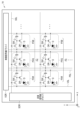
- FIG. 1 is a plan view showing a part of a display device according to a first embodiment of the present invention.
- FIG. 2 is an equivalent circuit diagram of the display device shown in FIG. 1.
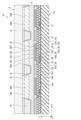
- FIG. 3 is a cross-sectional view of the display device shown in FIG. 1 taken along line III-III.
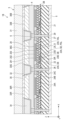
- FIG. 4 is a cross-sectional view of the display device shown in FIG. 1 taken along line IV-IV.
- FIG. 5 is a sectional view showing a part of a display device according to a second embodiment of the present invention.
- FIG. 1 is a plan view showing a part of a display device according to a first embodiment of the present invention.
- FIG. 2 is an equivalent circuit diagram of the display device shown in FIG. 1.
- FIG. 3 is a cross-sectional view of the display device shown in FIG. 1 taken along line III-III.
- FIG. 4 is a cross-sectional view of the display device shown in FIG. 1 taken along line IV-IV.
- the area surrounded by the broken line represents the opening on the transparent substrate 31 side of the first through hole that the black matrix 32 has, as will be described later.
- the display device 1A shown in FIGS. 1 to 4 is a micro-LED display capable of color display using an active matrix driving method, and in which each sub-pixel includes a light-emitting diode (LED).
- LED light-emitting diode
- the X direction and the Y direction are directions that are parallel to the display surface of the display device 1A and intersect with each other. According to one example, the X and Y directions are perpendicular to each other. Further, the Z direction is a direction perpendicular to the X direction and the Y direction. That is, the Z direction is the thickness direction of the display device 1A.
- the display device 1A includes a video signal line VSL, a power supply line PSL, a scanning signal line SSL, a pixel PX, a video signal line driver VDR, and a scanning signal line driver SDR. .
- the video signal line VSL and the power supply line PSL each extend in the Y direction and are arranged alternately in the X direction.
- the scanning signal lines SSL each extend in the X direction and are arranged in the Y direction.
- the pixels PX are arranged in the X direction and the Y direction.
- Each pixel PX includes a first sub-pixel PXR, a second sub-pixel PXG, and a third sub-pixel PXB.
- the first sub-pixel PXR, the second sub-pixel PXG, and the third sub-pixel PXB are arranged corresponding to the intersection of the video signal line VSL and the scanning signal line SSL.
- the first sub-pixel PXR, the second sub-pixel PXG, and the third sub-pixel PXB emit light of different colors.
- the first sub-pixel PXR, the second sub-pixel PXG, and the third sub-pixel PXB emit red light, green light, and blue light, respectively.
- the first sub-pixel PXR, the second sub-pixel PXG, and the third sub-pixel PXB are arranged in this order in the X direction.
- the arrangement order of the first sub-pixel PXR, second sub-pixel PXG, and third sub-pixel PXB in each pixel PX can be changed.
- first sub-pixel PXR, the second sub-pixel PXG, and the third sub-pixel PXB form a stripe arrangement.
- the first sub-pixel PXR, the second sub-pixel PXG, and the third sub-pixel PXB may form other arrangements such as a delta arrangement and a mosaic arrangement.
- Each of the first sub-pixel PXR, the second sub-pixel PXG, and the third sub-pixel PXB includes a light emitting element D, a drive control element DR, a switch SW, and a capacitor C.
- the light emitting element D is a light emitting diode.
- the light emitting diode is, for example, a light emitting diode made of an inorganic substance.
- a light emitting diode made of an inorganic substance can be obtained, for example, by dividing a laminate having a layer structure similar to these into a plurality of parts.
- the light emitting element D may be an electroluminescent element which is a light emitting diode made of an organic substance.
- the cathode of the light emitting element D is connected to a ground electrode.
- the light emitting element D is a blue light emitting diode that is made of an inorganic substance and emits blue light.
- the drive control element DR and switch SW are field effect transistors.
- the drive control element DR is a p-channel thin film transistor
- the switch SW is an n-channel thin film transistor.
- the drive control element DR has a gate connected to the drain of the switch SW, a source connected to the power supply line PSL, and a drain connected to the anode of the light emitting element D.
- the switch SW has a gate connected to the scanning signal line SSL, and a source connected to the video signal line VSL.
- the capacitor C is, for example, a thin film capacitor.
- the capacitor C has one electrode connected to the gate of the drive control element DR, and the other electrode connected to the power supply line PSL.
- the first sub-pixel PXR further includes a first wavelength conversion layer 36R and a first colored layer 33R shown in FIGS. 3 and 4.
- the first wavelength conversion layer 36R is installed to face the light emitting element D of the first sub-pixel PXR.
- the first wavelength conversion layer 36R converts the light emitted by the light emitting element D of the first sub-pixel PXR into first light of a specific color.
- the first wavelength conversion layer 36R converts, for example, blue light emitted by the light emitting element D of the first sub-pixel PXR into red light.
- the first colored layer 33R is installed to face the light emitting element D of the first sub-pixel PXR with the first wavelength conversion layer 36R in between.
- the first colored layer 33R transmits the light whose wavelength has been converted by the first wavelength conversion layer 36R, and absorbs the light whose wavelength has not been converted by the first wavelength conversion layer 36R.
- the first colored layer 33R is, for example, a red colored layer that transmits red light after wavelength conversion by the first wavelength conversion layer 36R and absorbs blue light etc. whose wavelength has not been converted by the first wavelength conversion layer 36R. .
- the second sub-pixel PXG further includes a second wavelength conversion layer 36G and a second colored layer 33G shown in FIG.
- the second wavelength conversion layer 36G is installed to face the light emitting element D of the second sub-pixel PXG.
- the second wavelength conversion layer 36G converts the light emitted by the light emitting element D of the second sub-pixel PXG into second light having a different color from the first light.
- the second wavelength conversion layer 36G converts, for example, blue light emitted by the light emitting element D of the second sub-pixel PXG into green light.
- the second colored layer 33G is installed to face the light emitting element D of the second sub-pixel PXG with the second wavelength conversion layer 36G in between.
- the second colored layer 33G transmits the light whose wavelength has been converted by the second wavelength conversion layer 36G, and absorbs the light whose wavelength has not been converted by the second wavelength conversion layer 36G.
- the second colored layer 33G is, for example, a green colored layer that transmits green light after wavelength conversion by the second wavelength conversion layer 36G and absorbs blue light, etc. whose wavelength has not been converted by the second wavelength conversion layer 36G. .
- the third sub-pixel PXB further includes a base layer 33B and a filling layer 36B shown in FIG. 3.
- the filling layer 36B is installed to face the light emitting element D of the third sub-pixel PXB.
- the filling layer 36B is, for example, a colorless and transparent layer.
- the filling layer 36B can be omitted.
- the base layer 33B is installed to face the light emitting element D of the third sub-pixel PXB with the filling layer 36B in between.
- the base layer 33B transmits the light emitted by the light emitting element D of the third sub-pixel PXB as third light.
- the base layer 33B is, for example, a colorless light transmitting layer or a blue colored layer that transmits blue light emitted from the light emitting element D of the third subpixel PXB.
- the video signal line driver VDR and the scanning signal line driver SDR are mounted on the display panel using COG (chip on glass), as shown in FIG.
- the video signal line driver VDR and the scanning signal line driver SDR may be implemented using TCP (tape carrier package) instead of COG implementation.
- a video signal line VSL and a power supply line PSL are connected to the video signal line driver VDR.
- the video signal line driver VDR outputs a voltage signal as a video signal to the video signal line VSL.
- a scanning signal line SSL is connected to the scanning signal line driver SDR.
- the scanning signal line driver SDR outputs a voltage signal as a scanning signal to the scanning signal line SSL.
- the power supply line PSL may be connected to the scanning signal line driver SDR instead of being connected to the video signal line driver VDR.
- the display device 1A will be explained in more detail.
- the display device 1A includes a light control device 2A, a black matrix substrate 3, and an adhesive layer 4, as shown in FIGS. 3 and 4.
- the light control device is a device that emits light toward the black matrix substrate and is capable of adjusting at least one of the intensity of this light and the time for emitting this light for each pixel or each subpixel.
- the substrate 21 includes, for example, an insulating substrate such as a glass substrate.
- the substrate 21 may further include an undercoat layer provided on the main surface of the insulating substrate facing the black matrix substrate 3.
- the undercoat layer is, for example, a laminate of a silicon nitride layer and a silicon oxide layer that are sequentially stacked on an insulating substrate.
- the substrate 21 may be a semiconductor substrate such as a silicon substrate.
- the substrate 21 may be rigid or flexible.
- the semiconductor layers 22 are arranged on the main surface of the substrate 21 facing the black matrix substrate 3.
- the semiconductor layer 22 is, for example, a polysilicon layer.
- the semiconductor layer 22 is a semiconductor layer of a thin film transistor that constitutes the drive control element DR or the switch SW.
- Each semiconductor layer 22 includes a source and a drain, and a channel region interposed therebetween.
- the conductor layer 23A is a conductor pattern provided on the main surface of the substrate 21.
- the conductor layer 23A constitutes the video signal line VSL, the power supply line PSL, the source electrode SE, the drain electrode DE, and the lower electrode (not shown) of the capacitor C.
- the source electrode SE and the drain electrode DE are connected to the source and drain of the semiconductor layer 22, respectively.
- the conductor layer 23A is made of metal or an alloy.
- the conductor layer 23A may have a single layer structure or a multilayer structure.
- the insulating layer 24A covers the conductor layer 23A and the main surface of the substrate 21.
- the insulating layer 24A can be formed using, for example, TEOS (tetraethyl orthosilicate).
- TEOS tetraethyl orthosilicate
- the gate insulating film of each thin film transistor constituting the drive control element DR or switch SW is a part of the insulating layer 24A. Further, the dielectric layer of each capacitor C is another part of the insulating layer 24A.
- the conductor layer 23B is a conductor pattern provided on the insulating layer 24A.
- the gate electrode GE of each thin film transistor constituting the drive control element DR or switch SW is a part of the conductor layer 23B.
- Each gate electrode GE faces the channel region of the semiconductor layer 22 with the insulating layer 24A in between.
- the upper electrode (not shown) of each capacitor C is another part of the conductor layer 23B.
- Each upper electrode faces the lower electrode of the capacitor C including the upper electrode, with the insulating layer 24A interposed therebetween.
- the conductor layer 23B is made of metal or an alloy.
- the conductor layer 23B may have a single layer structure or a multilayer structure.
- the insulating layer 24B covers the conductor layer 23B and the insulating layer 24A.
- the insulating layer 24B is an interlayer insulating film.
- the insulating layer 24B is made of, for example, an inorganic insulator such as silicon oxide.
- the insulating layer made of an inorganic insulator can be formed by, for example, a plasma CVD (chemical vapor deposition) method.
- the conductor layer 23C is a conductor pattern provided on the insulating layer 24B, as shown in FIG.
- the conductor layer 23C constitutes a scanning signal line SSL.
- the source electrode SE and the drain electrode DE may be provided on the insulating layer 24B instead of being provided on the insulating layer 24A. That is, the conductor layer 23C may constitute the scanning signal line SSL, the source electrode SE, and the drain electrode DE.
- the insulating layer 24C covers the conductor layer 23C and the insulating layer 24B.
- the insulating layer 24C is a passivation film.
- the insulating layer 24C is made of an inorganic insulator such as silicon nitride, for example.
- the conductor layer 23D is a conductor pattern provided on the insulating layer 24C.
- the conductor layer 23D constitutes electrode pads arranged in the X direction and the Y direction corresponding to the first sub-pixel PXR, the second sub-pixel PXG, and the third sub-pixel PXB.
- a through hole is provided in the stacked body consisting of the insulating layers 24A, 24B, and 24C at the position of the drain electrode DE connected to the drain of the drive control element DR. Each electrode pad is connected to the drain electrode DE through this through hole.
- the conductor layer 23D is made of metal or an alloy, for example.
- the conductor layer 23D may have a single layer structure or a multilayer structure.
- the contour of the orthogonal projection of each electrode pad onto a plane perpendicular to the Z direction is spaced apart from the orthogonal projection of the light emitting element 25 installed on this electrode pad onto the plane above, and surrounds this orthogonal projection.
- the electrode pad has a larger dimension in the direction perpendicular to the Z direction than the light emitting element 25. Therefore, the electrode pad also serves as a reflective layer that reflects light traveling toward the substrate 21.
- the electrode pad does not have to play the role of this reflective layer. In this case, the reflective layer that plays this role may be provided separately from the electrode pad, or may not be provided.
- the light emitting element 25 shown in FIGS. 3 and 4 is the light emitting element D shown in FIG. 2.
- the light emitting element 25 is arranged on the electrode pad.
- the light emitting element 25 is a light emitting diode made of an inorganic material.
- a substrate including a light emitting diode as the light emitting element 25 is sometimes referred to as an "LED substrate.”
- the light emitting element 25 has a multilayer structure including a plurality of layers, for example, a first layer 251, a second layer 252, and a third layer 253.
- the stacking direction of the layers included in the light emitting element 25 is the Z direction. This stacking direction may be perpendicular to the Z direction.
- Each light emitting element 25 includes an anode and a cathode.
- the light emitting element 25 has an anode and a cathode on one surface.
- the anode of the light emitting element 25 is connected to an electrode pad via a bonding wire (not shown).
- the bonding of the light emitting element 25 to the electrode pad and the connection of the anode to the electrode pad are performed using a conductive paste such as a conductive paste.
- the bonding may also be performed by die bonding using the material as a bonding material.
- the conductor layer 28 is omitted, and an electrode pad for connecting to the cathode of the light emitting element 25 is further provided on the insulating layer 24C, and these electrodes are Wiring connected to the pads may be further provided between the insulating layers, and the connection of the light emitting element 25 to the electrode pad and the conductor layer 28 and the connection of the anode and cathode to the electrode pads may be performed by flip chip bonding.
- the dimensions of the light emitting element 25 in the X and Y directions are preferably in the range of 1 to 100 ⁇ m, more preferably in the range of 5 to 80 ⁇ m, and still more preferably in the range of 10 to 60 ⁇ m.
- the dimension of the light emitting element 25 in the Z direction is preferably in the range of 1 to 20 ⁇ m, more preferably in the range of 1 to 15 ⁇ m, and still more preferably in the range of 1 to 10 ⁇ m.
- the partition layer 26 is provided on the insulating layer 24C.
- the partition layer 26 has through holes at the positions of the electrode pads.
- the light emitting elements 25 are located within these through holes, respectively.
- the partition layer 26 is made of resin, for example.
- Such a partition layer 26 can be formed by photolithography using a photosensitive resin.
- the partition layer 26 may include a resin layer having through holes, and a reflective layer covering the side walls of the through holes and optionally the upper surface of the resin layer.
- the reflective layer may have a single layer structure or a multilayer structure.
- the reflective layer includes, for example, a metal, an alloy, or a transparent dielectric.
- the partition layer 26 can be omitted.
- the filling layer 27 fills the gap between the light emitting element 25 and the partition layer 26.
- the filling layer 27 is a light transmitting layer that transmits the light emitted from the light emitting element 25. Furthermore, the filling layer 27 also serves as a protective layer that protects the light emitting element 25 and the joints between it and the electrodes.
- the filling layer 27 is made of resin, for example.
- the refractive index of the filling layer 27 is preferably different from the refractive index of the material forming the surface of the partition layer 26.
- the conductor layer 28 is provided on the partition layer 26 and the filling layer 27.
- the cathode of the light emitting element 25 is connected to the conductor layer 28.
- the conductor layer 28 is made of a conductive transparent oxide, it can be provided so as to cover the entire cathode of the light emitting element 25 .
- the conductor layer 28 is made of metal or an alloy, it is preferable to provide the conductor layer 28 so as to partially cover the cathode of the light emitting element 25 .
- the black matrix substrate 3 faces the light control device 2A. Specifically, the black matrix substrate 3 faces the substrate 21 with the light emitting elements 25 and the like interposed therebetween.
- the black matrix substrate 3 includes a transparent substrate 31, a black matrix 32, a resin layer 34, a reflective layer 35, a color filter including a first colored layer 33R and a second colored layer 33G, a base layer 33B, and a color filter including a first colored layer 33R and a second colored layer 33G. It includes a first wavelength conversion layer 36R, a second wavelength conversion layer 36G, and a filling layer 36B.
- the transparent substrate 31 has visible light transmittance.
- the transparent substrate 31 is, for example, a colorless substrate.
- the transparent substrate 31 may have a single layer structure or a multilayer structure.
- the transparent substrate 31 is made of, for example, glass, transparent resin, or a combination thereof.
- the transparent substrate 31 may be hard or flexible.
- the transparent substrate 31 has a first main surface facing the light control device 2A and a second main surface that is the back surface thereof.
- the black matrix 32 is provided on the first main surface of the transparent substrate 31.
- the black matrix 32 is a black layer that blocks visible light.
- the black matrix 32 is made of, for example, a mixture containing a binder resin and a colorant.
- the coloring agent is, for example, a black pigment or a mixture of pigments that produces a black color by subtractive color mixing, for example a mixture containing a blue pigment, a green pigment and a red pigment.
- the black matrix 32 is a layer containing carbon materials such as graphite, graphene, and carbon nanotubes.
- the black matrix 32 is a laminate of a chromium layer and a chromium oxide layer.
- the black matrix 32 has a first through hole at the position of the light emitting element 25.
- the opening of each first through hole on the transparent substrate 31 side has a larger dimension in the direction perpendicular to the Z direction than the light emitting element 25 .
- each portion of the black matrix 32 corresponding to the pixel PX includes a first through hole provided at the position of the first sub pixel PXR, a first through hole provided at the position of the second sub pixel PXG, and a third through hole provided at the position of the second sub pixel PXG. and a first through hole provided at the position of the sub-pixel PXB, and these three first through holes are arranged in the X direction.
- a plurality of first through-hole groups each consisting of these three first through-holes are arranged in the X direction and the Y direction.
- the distance between adjacent first through-hole groups in the X direction is larger than the distance between first through-holes included in the same through-hole group.
- the distance between adjacent first through-hole groups in the Y direction is also larger than the distance between first through-holes included in the same through-hole group.
- the aperture ratio of the black matrix 32 is preferably within the range of 5 to 66%, more preferably within the range of 5 to 40%, and still more preferably within the range of 5 to 20%.
- a light emitting diode made of an inorganic material can emit bright light even if the light exit surface is small, and has a long life. Therefore, when the light emitting element 25 is a light emitting diode made of an inorganic material, bright display is possible even if the aperture ratio of the black matrix 32 is made small.
- the aperture ratio of the black matrix 32 is reduced, reflection of external light can be suppressed, black color with greater depth can be displayed, and a higher contrast ratio can therefore be achieved.
- the thickness of the black matrix 32 is preferably in the range of 0.1 to 30 ⁇ m, more preferably in the range of 1 to 15 ⁇ m, and still more preferably in the range of 1 to 5 ⁇ m.
- a thick black matrix 32 is advantageous in achieving high light-shielding properties.
- the black matrix 32 is made thicker, during pattern exposure of a coating film made of a photosensitive black composition, light may not be able to reach deep parts of the coating film with sufficient intensity, and high shape accuracy may not be achieved. .
- the resin layer 34 is provided on the black matrix 32, as shown in FIGS. 3 and 4.
- resin layer 34 is transparent.
- the resin layer 34 may be colored or colorless.
- the resin layer 34 may have light scattering properties. For example, assuming that the film thickness is 5 ⁇ m, the transparent resin layer 34 has a maximum transmittance of 20% or more for light in the wavelength range of 350 to 480 nm that is incident in the thickness direction. It is desirable that
- the resin layer 34 has second through holes at the positions of the first through holes. These second through holes constitute a second through hole group corresponding to the first through hole group described above.
- Each of the second through-hole groups here includes three second through-holes arranged in the X direction.
- the second through-hole group is arranged in a first direction and a second direction that intersect with each other, here, in the X direction and the Y direction.
- the distance W x 1 between the second through-hole groups adjacent to each other in the X direction is larger than the distance W1 between the second through-holes included in the same through-hole group.
- the distance W y 1 between the second through-hole groups adjacent to each other in the Y direction is also larger than the distance W 1 between the second through-holes included in the same through-hole group.
- the distance W1 is preferably in the range of 5 to 80 ⁇ m, more preferably in the range of 5 to 40 ⁇ m, and still more preferably in the range of 5 to 20 ⁇ m.
- the distance W x 1 is preferably in the range of 5 to 250 ⁇ m, more preferably in the range of 50 to 250 m, even more preferably in the range of 100 to 250 ⁇ m.
- the distance W y 1 is preferably in the range of 5 to 250 ⁇ m, more preferably in the range of 5 to 100 ⁇ m, and still more preferably in the range of 5 to 50 ⁇ m.
- the ratio W x 1/W1 between the distance W x 1 and the distance W1 is preferably in the range of 0.1 to 50, more preferably in the range of 2 to 20, and still more preferably in the range of 5 to 15. It's within.
- the distance W x 1 may be equal to the distance W1 or may be smaller than the distance W1.
- the ratio W y 1/W1 between the distance W y 1 and the distance W1 is preferably in the range of 0.1 to 50, more preferably in the range of 0.1 to 10, and even more preferably 0.1. It is within the range of 5 to 5.
- the distance W y 1 may be equal to the distance W1 or may be smaller than the distance W1.
- the contour of the orthogonal projection of the opening on the transparent substrate 31 side onto the first principal surface of the second through hole is the contour of the orthogonal projection of the opening on the transparent substrate 31 side onto the first principal surface. It is provided so as to surround the projection contour (hereinafter referred to as the first contour).
- the second contour does not have to surround the first contour. In a structure in which the second contour surrounds the first contour, stray light has less influence on the display than in a structure in which the second contour does not surround the first contour.
- a portion of the resin layer 34 sandwiched between adjacent second through holes has a forward tapered cross-sectional shape.
- This portion may have a rectangular cross-sectional shape, a reverse tapered cross-sectional shape, or another cross-sectional shape.
- the thickness of the resin layer 34 is preferably in the range of 5 to 50 ⁇ m, more preferably in the range of 5 to 40 ⁇ m, and still more preferably in the range of 10 to 25 ⁇ m.
- the thickness of the resin layer 34 is small, it is difficult to increase the total thickness of the layers formed in the second through hole.
- the resin layer 34 is made thicker, the shape accuracy of the partition wall portion sandwiched between adjacent second through holes is reduced.
- the reflective layer 35 at least partially covers the side walls of each of the second through holes and the upper surface of the resin layer 34.
- the reflective layer 35 covers the entire side wall of each second through hole, the entire upper surface of the resin layer 34, and the part of the black matrix 32 that is not covered with the resin layer 34. It covers the parts.
- the reflective layer 35 does not need to cover a part of the side wall of the second through hole.
- the reflective layer 35 covers at least one of a portion of at least one side wall of the second through hole near the black matrix 32 and a portion of at least one side wall of the second through hole near the top surface of the resin layer 34. It does not need to be covered.
- the reflective layer 35 does not need to cover the portions of the black matrix 32 that are not covered with the resin layer 34 .
- the portion of the reflective layer 35 located within the second through-hole is open at the position of the first colored layer 33R, the second colored layer 33G, or the base layer 33B.
- the area S2 of each of these openings is preferably larger compared to the area S1 of the opening of the first through hole.
- the ratio S2/S1 between area S2 and area S1 is preferably in the range of 1 to 100, more preferably in the range of 1 to 30, and still more preferably in the range of 1 to 2.
- the reflective layer 35 may have a single layer structure or a multilayer structure.
- the layer included in the reflective layer 35 is, for example, a metal, an alloy, or a transparent dielectric. From the viewpoint of thermal conductivity, the reflective layer 35 preferably includes a layer made of metal or an alloy. According to one example, the reflective layer 35 consists of aluminum, an aluminum alloy or a neodymium alloy.
- the thickness of the reflective layer 35 at the portion covering the upper surface of the resin layer 34 is preferably within the range of 100 to 500 nm, more preferably within the range of 100 to 250 nm. Increasing the thickness of the reflective layer 35 improves the thermal conductivity in the in-plane direction. However, increasing the thickness of the reflective layer 35 increases manufacturing costs.
- the reflective layer 35 can be formed by, for example, forming a film by a vapor deposition method such as a sputtering method or a vacuum evaporation method, forming an etching mask, and etching such as wet etching in this order.
- the etching mask can be formed by photolithography using a photosensitive resin.
- the transparent resin layer used as this etching mask may or may not be removed after the above etching.
- the first colored layer 33R fills the first through hole at the position of the first sub-pixel PXR, as shown in FIGS. 3 and 4. As mentioned above, the first colored layer 33R is a red colored layer here.
- the second colored layer 33G fills the first through hole at the position of the second sub-pixel PXG.
- the second colored layer 33G is a green colored layer here.
- the base layer 33B embeds the first through hole at the position of the third sub-pixel PXB.
- the base layer 33B is a colorless light-transmitting layer or a blue-colored layer.
- the first wavelength conversion layer 36R is provided on the first colored layer 33R, and buries at least the bottom of the second recess.
- the first wavelength conversion layer 36R is a layer containing a phosphor such as a quantum dot phosphor and a transparent resin. As described above, here, the first wavelength conversion layer 36R converts the blue light emitted by the light emitting element D of the first sub-pixel PXR into red light.
- the second wavelength conversion layer 36G is provided on the second colored layer 33G, and buries at least the bottom of the second recess.
- the second wavelength conversion layer 36G is a layer containing a phosphor such as a quantum dot phosphor and a transparent resin. As described above, here, the second wavelength conversion layer 36G converts the blue light emitted by the light emitting element D of the second sub-pixel PXG into red light.
- the filling layer 36B is provided on the base layer 33B and fills at least the bottom of the second recess.
- the filling layer 36B is a colorless and transparent layer here.
- the filling layer 36B is made of transparent resin, for example.
- the adhesive layer 4 is interposed between the light control device 2A and the black matrix substrate 3, and adheres them to each other.
- the adhesive layer 4 transmits the light emitted by the light emitting element 25.
- the adhesive layer 4 is, for example, a colorless and transparent layer.
- the adhesive layer 4 is made of adhesive or adhesive.
- the portion of the reflective layer 35 that covers the upper surface of the resin layer 34 has an arithmetic mean height S a in the range of 40 to 650 nm, and a kurtosis S ku of 3 or more.
- the portion of the reflective layer 35 that covers the side wall of the second through hole provided in the resin layer 34 also has an arithmetic average height S a within the range of 40 to 650 nm, and a kurtosis S ku of 3 or more. be. It is preferable that these arithmetic mean heights S a are 100 nm or more, and it is also preferable that it is 400 nm or less. Further, these kurtosis S ku are, for example, 6 or less. Note that the kurtosis S ku represents the sharpness of the height distribution.
- the light emitting element 25 is the main heat generation source. A portion of the heat generated in the light emitting element 25 is transmitted to the reflective layer 35 via the adhesive layer 4.
- the difference between the adhesive layer 4 and the reflective layer 35 is greater than when this part is smoother. heat exchange can occur more efficiently.
- the reflective layer 35 has particularly excellent thermal conductivity among the elements located between the adhesive layer 4 and the transparent substrate 31.
- the reflective layer 35 covers not only the upper surface of the resin layer 34 but also the side walls of the through holes provided in the resin layer 34, and also partially covers the black matrix 32.
- the reflective layer 35 includes a portion located near the transparent substrate 31 in addition to a portion adjacent to the adhesive layer 4 .
- the black matrix 32 interposed between the reflective layer 35 and the transparent substrate 31 is made of a black material such as carbon-containing resin or chromium oxide. These black materials have high thermal conductivity. Therefore, the heat transmitted from the adhesive layer 4 to the reflective layer 35 is quickly transmitted to the transparent substrate 31.
- the display device 1A can quickly radiate part of the heat generated in the light emitting elements 25 to the outside air via the black matrix substrate 3. Therefore, this display device 1A is difficult to accumulate heat inside and has excellent heat dissipation.
- the display device 1A Since the display device 1A has excellent heat dissipation properties as described above, it is difficult to cause deterioration, decrease in brightness, and color shift, as described below.
- wavelength shift In recent years, in order to expand the use of display devices, there is a need for display devices with increased output and high brightness in order to improve outdoor visibility.
- the heat generated by the light emitting diode may cause problems such as thermal deterioration of members such as wiring and sealing resin located near the light emitting diode.
- phosphors such as quantum dots undergo thermal deterioration, as well as a decrease in brightness and color shift when emitting light at high temperatures (shift in wavelength showing maximum intensity in the visible range; hereinafter referred to as wavelength shift).
- the light emitting diode which is the heat source
- the light emitting diode is isolated from the atmosphere, so heat is stored inside.
- high-brightness display uses phosphors such as quantum dots to convert the short wavelength light (blue light or ultraviolet light) emitted by light-emitting diodes into blue, green, and red light for full-color display.
- Equipment requires excellent heat dissipation.
- the display device 1A described above quickly radiates part of the heat generated in the light emitting elements 25 to the outside of the display device 1A via the black matrix substrate 3. Therefore, in this display device 1A, heat does not easily accumulate inside the display device 1A, and the inside temperature does not easily reach an excessively high temperature. Therefore, the display device 1A is less likely to cause deterioration of quantum dots, etc., decrease in brightness, and color shift (wavelength shift).
- the portion of the reflective layer 35 that covers the side wall of the second through hole provided in the resin layer 34 has the above-mentioned surface texture, this portion will moderately scatter the light from the light emitting element 25. can be done. As a result, the wavelength conversion efficiency in the first wavelength conversion layer 36R and the second wavelength conversion layer 36G increases, making it possible to increase brightness or reduce power consumption.
- the reflective layer 35 having the above-mentioned surface properties can be obtained by, for example, subjecting the resin layer 34 to surface roughening treatment such as O 2 plasma treatment, and then forming the reflective layer 35 into a film. That is, by performing the surface roughening treatment, the arithmetic mean height S a and the kurtosis S ku of the resin layer 34 can be increased, and therefore the arithmetic mean height S a and the kurtosis S ku of the reflective layer 35 can also be increased. It can be made larger. For example, by subjecting a resin layer having an arithmetic mean height S a of 30 nm to O 2 plasma treatment, the reflective layer 35 having an arithmetic mean height S a of 40 nm or more can be obtained.
- surface roughening treatment such as O 2 plasma treatment
- the reflective layer 35 having the above-mentioned surface properties can also be obtained by incorporating particles into the material of the resin layer 34. By appropriately setting the particle size and content of the particles, it is possible to obtain the resin layer 34 having the desired surface texture, and therefore to obtain the reflective layer 35 having the above-mentioned surface texture. is also possible.
- these particles are preferably made of a highly thermally conductive material such as a metal oxide. In this case, the thermal conductivity of the resin layer 34 is increased and the heat dissipation is improved.
- the proportion of particles in this material is preferably 50% by volume or less, more preferably 20% by volume or less. If this ratio is increased, the shape accuracy of the resin layer 34 will decrease.
- the portion of the reflective layer 35 that covers the side wall of the second through hole provided in the resin layer 34 has an arithmetic mean height S a that is the same as the wavelength in the visible range. It is preferable that the degree of
- the arithmetic mean height S a of the portion of the reflective layer 35 that covers the upper surface of the resin layer 34 and the portion that covers the side wall of the second through hole provided in the resin layer 34 is not excessively large. is desirable.
- etching residue is likely to be generated.
- the arithmetic mean height S a of the resin layer 34 is excessively increased, the removability of the protective resist used as a mask during this etching will be reduced.
- the black matrix substrate 3 includes a partition layer consisting of a resin layer 34 provided with a second through hole and a reflective layer 35 covering the resin layer 34.
- the structure in which a black matrix substrate is provided with a partition layer including a resin layer having through holes and a metal layer covering the resin layer is advantageous for repairing the LED substrate before bonding the LED substrate and the black matrix substrate. It is. This will be explained below.
- a protective film can also be formed on the light emitting diode.
- the LED substrate cannot be repaired, resulting in a reduction in yield.
- partition layer including a resin layer having through holes and a metal layer covering the resin layer
- a partition wall can be omitted from the LED board. Therefore, ease of manufacture, high reflectance, and high light shielding properties can be achieved without reducing yield.
- FIG. 5 is a sectional view showing a part of a display device according to a second embodiment of the present invention.
- the display device 1B shown in FIG. 5 is the same as the display device 1A described above except that the following configuration is adopted. That is, the display device 1B includes a light control device 2B that is similar to the light control device 2A except that one or more through holes each extending in the Z direction are provided instead of the light control device 2A. .
- the display device 1B further includes a heat radiator 5 and a heat conductor.
- the heat sink 5 is located outside the laminate of the light control device 2A, the black matrix substrate 3, and the adhesive layer 4.
- the heat radiator 5 is a back heat radiator provided to face the black matrix substrate 3 with the light control device 2B and the adhesive layer 4 in between.
- the heat dissipation body 5 is a back heat dissipation layer provided on the light control device 2B here.
- the heat sink 5 is made of a highly thermally conductive material.
- Highly thermally conductive materials include, for example, metals such as copper, aluminum, iron, silver, titanium, molybdenum, tantalum, tungsten, and niobium; alloys containing one or more of these metals; carbides such as tungsten carbide; graphite, graphene, Carbon materials such as carbon nanotubes and diamonds; other insulating ceramics; or composite materials containing one or more of them.
- the heat sink 5 may have a single layer structure or a multilayer structure.
- the heat sink 5 has a flat surface.
- the heat sink 5 having a flat surface can be formed by, for example, forming a film on the light control device 2A.
- the heat sink 5 having a flat surface can be provided on the light control device B by pasting it on the light control device 2B.
- the heat radiator 5 having a flat surface is easy to form or install on the light control device 2B.
- the heat sink 5 may have an uneven surface.
- the heat sink 5 may have a plurality of fins or pins on its surface.
- Such a heat sink 5 has a large surface area and is excellent in heat dissipation.
- the ratio S RB /S B of the apparent area S RB of the heat sink 5 (area not taking into account irregularities) and the area S B of the back surface of the light control device 2A is preferably 0.05 or more, and 0.05 or more. More preferably, it is 5 or more.
- the upper limit value of the ratio S RB /S B is, for example, 1.
- the ratio S RB /S B may be greater than 1.
- the minimum thickness of the heat sink 5 is preferably 50 ⁇ m or more, more preferably 500 ⁇ m or more.
- the minimum thickness of the heat sink 5 is increased, the heat capacity of the heat sink 5 increases, and the thermal resistance of the heat sink 5 decreases.
- the minimum thickness of the heat sink 5 is 5 mm or less.
- the heat transfer body is provided inside the laminate.
- the heat transfer body guides heat from the reflective layer 35 to the heat dissipation body 5.
- the heat transfer body here consists of a main heat transfer body 29 and an auxiliary heat transfer body 6. Moreover, here, the heat transfer body is located at least partially within the through hole of the light control device 2B.
- the main heat transfer body 29 is made of a highly thermally conductive material that fills the through holes provided in the light control device 2B.
- the main heat transfer body 29 may be one in which the side wall of a through hole provided in the light control device 2B is coated with a highly thermally conductive material.
- the main heat transfer body 29 promotes heat transfer from the reflective layer 35 to the heat dissipation body 5.
- the auxiliary heat transfer body 6 is installed between the main heat transfer body 29 and the reflective layer 35.
- the auxiliary heat transfer body 6 is made of a highly thermally conductive material.
- the auxiliary heat transfer body 6 promotes heat transfer from the reflective layer 35 to the main heat transfer body 29.
- the auxiliary heat transfer body 6 can be omitted.
- the main heat transfer body 29 and the auxiliary heat transfer body 6 are made of a highly thermally conductive material.
- the highly thermally conductive material for example, those exemplified for the heat sink 5 can be used.
- Each of the main heat transfer body 29 and the auxiliary heat transfer body 6 may have a single layer structure or a multilayer structure.
- the light emitting element 25 is the main heat source.
- the other part of the heat generated in the light emitting element 25 is radiated to the outside air via the black matrix substrate 3, similarly to the display device 1A.
- Another part of the heat generated in the light emitting element 25 is guided to the heat sink 5 installed outside the laminate via the reflective layer 35 and the heat transfer body. Therefore, this display device 1B is less likely to accumulate heat inside the laminate, and is particularly excellent in heat dissipation.
- the heat sink 5 since the heat sink 5 is provided on the back surface, the heat sink 5 does not interfere with display. Therefore, various structures can be adopted for the heat sink 5.
- a partition layer including a resin layer having through holes and a metal layer covering the resin layer is provided on the black matrix substrate, so a large partition wall can be formed on the LED substrate.
- the partition wall can be omitted from the LED board. Therefore, ease of manufacture, high reflectance, and high light shielding properties can be achieved without reducing yield.
- the heat transfer body that thermally connects the reflective layer 35 and the heat dissipation body 5 is at least partially located outside the laminate of the light control device 2B, the black matrix substrate 3, and the adhesive layer 4. You may provide it so that it may be located.
- the heat transfer body may be provided on the end face of the laminate.
- the display device 1A further includes a front heat dissipation layer as a heat dissipation body, which is provided on the second main surface of the transparent substrate 31 and is open at the position of the first through hole provided in the black matrix 32.
- the display device 1A may further include a heat conductor that thermally connects the reflective layer 35 and the front heat dissipation layer.
- the heat transfer body may be provided inside the laminate of the light control device 2A, the black matrix substrate 3, and the adhesive layer 4, or may be provided at least partially outside the laminate.
- the display device In an electronic device that includes a display device, the display device is usually installed in a casing so that its front surface is exposed to the outside of the electronic device, and its back surface is adjacent to the internal space of the casing. Therefore, when the display device 1A provided with a front heat dissipation layer as a heat dissipation body is mounted on an electronic device, heat exchange is likely to occur between the heat dissipation body and the outside air.
- the display device 1B may also further include the above-mentioned front heat dissipation layer.
- the display device 1B may further include a heat conductor that thermally connects the reflective layer 35 and the front heat dissipation layer.
- the video signal line driver VDR may supply a current signal as a video signal to the video signal line VSL.
- the gate-source voltage of the drive control element DR is equal to this current signal. It may be set to a corresponding value, and a drive current having a magnitude corresponding to the gate-source voltage may be caused to flow through the light emitting element D during the light emitting period.
- a circuit for displaying an image using a passive matrix drive method may be used in the light control devices 2A and 2B.
- the filling layer 36B is a wavelength conversion layer that converts the light emitted by the light emitting element 25 of the third sub-pixel PXB into third light having a different color from the first light and the second light.
- the first wavelength conversion layer 36R, the second wavelength conversion layer 36G, and the filling layer 36B convert the ultraviolet light emitted by the light emitting element 25 into red light, green light, and blue light, respectively.
- multiple types of light emitting diodes may be used, for example, in the first subpixel PXR, the second subpixel PXG, and the third subpixel PXB. , a red light emitting diode, a green light emitting diode and a blue light emitting diode, respectively.
- a layer similar to that described above for the base layer 33B is provided instead of the first colored layer 33R and the second colored layer 33G, and a filling layer is provided instead of the first wavelength conversion layer 36R and the second wavelength conversion layer 36G. Layers similar to those described above for layer 36B may be provided.
- the display device may also display a monochrome image.
- the first sub-pixel PXR and the second sub-pixel PXG are omitted, a blue light emitting diode is used as the light emitting element 25, and the filling layer 36B is a wavelength conversion layer that converts blue light into yellow light. do.
- the filling layer 36B converts a part of the blue light incident thereon into yellow light and transmits the rest, it is possible to display white by additive color mixing of blue and yellow.
- the black matrix substrate may further include an overcoat layer interposed between the black matrix 32 and the resin layer 34.
- the overcoat layer can include a transparent resin and one or more of a UV absorber, a yellow pigment, and transparent particles.
- the overcoat layer containing an ultraviolet absorber can absorb ultraviolet light when the stray light incident on the resin layer 34 is ultraviolet light.
- Light emitting element DR...drive control element, PSL...power supply line, PX...pixel, PXB...third sub-pixel, PXG...second sub-pixel, PXR...first sub-pixel, SDR...scanning signal line driver, SSL...scanning signal line, SW...switch, VDR...video signal line driver, VSL...video signal line.
Landscapes
- Physics & Mathematics (AREA)
- General Physics & Mathematics (AREA)
- Optics & Photonics (AREA)
- Engineering & Computer Science (AREA)
- Theoretical Computer Science (AREA)
- Devices For Indicating Variable Information By Combining Individual Elements (AREA)
- Electroluminescent Light Sources (AREA)
- Led Device Packages (AREA)
- Optical Filters (AREA)
Abstract
Description
図1は、本発明の第1実施形態に係る表示装置の一部を示す平面図である。図2は、図1に示す表示装置の等価回路図である。図3は、図1に示す表示装置のIII-III線に沿った断面図である。図4は、図1に示す表示装置のIV-IV線に沿った断面図である。なお、図1において、破線で囲まれた領域は、後述するように、ブラックマトリクス32が有している第1貫通孔の透明基板31側の開口を表している。
表示装置1Aは、図3及び図4に示すように、調光装置2Aと、ブラックマトリクス基板3と、接着層4とを含んでいる。
図5は、本発明の第2実施形態に係る表示装置の一部を示す断面図である。
図5に示す表示装置1Bは、以下の構成を採用したこと以外は、上述した表示装置1Aと同様である。即ち、表示装置1Bは、調光装置2Aの代わりに、Z方向へ各々が伸びた1以上の貫通孔が設けられていること以外は調光装置2Aと同様の調光装置2Bを含んでいる。また、表示装置1Bは、放熱体5及び伝熱体を更に含んでいる。
上述した表示装置及びブラックマトリクス基板には、以下に例示するように、様々な変形が可能である。
例えば、映像信号線ドライバVDRは、映像信号線VSLへ映像信号として電流信号を供給するものであってもよい。この場合、第1サブ画素PXR、第2サブ画素PXG、及び第3サブ画素PXBの各々は、映像信号を書き込む書込期間においては、駆動制御素子DRのゲート-ソース間電圧がこの電流信号に対応した値に設定され、発光期間においては、上記ゲート-ソース間電圧に対応した大きさの駆動電流を発光素子Dへ流すように構成してもよい。また、調光装置2A及び2Bには、アクティブマトリクス駆動方式により画像を表示するための回路を採用する代わりに、パッシブマトリクス駆動方式により画像を表示するための回路を採用してもよい。
Claims (13)
- 第1主面及び第2主面を有している透明基板と、
前記第1主面上に設けられ、複数の第1貫通孔を有しているブラックマトリクスと、 前記ブラックマトリクス上に設けられ、前記複数の第1貫通孔の位置に複数の第2貫通孔をそれぞれ有している樹脂層と、
前記複数の第2貫通孔の各々の側壁と前記樹脂層の上面とを少なくとも部分的に被覆した反射層と
を含み、
前記反射層のうち前記上面を被覆した部分は、算術平均高さSaが40乃至650nmの範囲内にあり、クルトシスSkuが3以上であるブラックマトリクス基板。 - 前記反射層のうち前記側壁を被覆した部分は、算術平均高さSaが40乃至650nmの範囲内にあり、クルトシスSkuが3以上である請求項1に記載のブラックマトリクス基板。
- 前記反射層は、前記ブラックマトリクスを部分的に更に被覆した請求項1又は2に記載のブラックマトリクス基板。
- 前記複数の第2貫通孔の少なくとも一部の中にそれぞれ設けられた複数の波長変換層を更に含んだ請求項1乃至3の何れか1項に記載のブラックマトリクス基板。
- 前記複数の第1貫通孔の少なくとも一部の位置にそれぞれ配置された複数の着色層を含んだカラーフィルタを更に含んだ請求項1乃至4の何れか1項に記載のブラックマトリクス基板。
- 前記反射層は、金属又は合金からなる層を含んだ請求項1乃至5の何れか1項に記載のブラックマトリクス基板。
- 請求項1乃至6の何れか1項に記載のブラックマトリクス基板と、
前記第1主面と向き合うように設置された調光装置と、
前記ブラックマトリクス基板と前記調光装置との間に介在して、それらを貼り合わせた接着層と
を備えた表示装置。 - 前記ブラックマトリクス基板と前記調光装置と前記接着層との積層体の外部に位置した放熱体と、
前記反射層から前記放熱体へ熱を導く伝熱体と
を更に備えた請求項7に記載の表示装置。 - 前記放熱体は、前記調光装置及び前記接着層を間に挟んで前記ブラックマトリクス基板と向き合うように設けられた裏面放熱体を含んだ請求項8に記載の表示装置。
- 前記裏面放熱体は、前記調光装置上に設けられた裏面放熱層である請求項9に記載の表示装置。
- 前記調光装置には1以上の貫通孔が設けられ、前記伝熱体は、少なくとも部分的に前記1以上の貫通孔内に位置した請求項8乃至10の何れか1項に記載の表示装置。
- 前記調光装置は複数の発光素子を含んだ請求項7乃至11の何れか1項に記載の表示装置。
- 前記調光装置は複数の発光ダイオードを含んだ請求項7乃至12の何れか1項に記載の表示装置。
Priority Applications (2)
| Application Number | Priority Date | Filing Date | Title |
|---|---|---|---|
| KR1020257009703A KR20250056968A (ko) | 2022-08-31 | 2023-08-17 | 표시 장치 |
| CN202380048588.5A CN119422085A (zh) | 2022-08-31 | 2023-08-17 | 显示装置 |
Applications Claiming Priority (2)
| Application Number | Priority Date | Filing Date | Title |
|---|---|---|---|
| JP2022138481A JP7452592B1 (ja) | 2022-08-31 | 2022-08-31 | 表示装置 |
| JP2022-138481 | 2022-08-31 |
Publications (1)
| Publication Number | Publication Date |
|---|---|
| WO2024048312A1 true WO2024048312A1 (ja) | 2024-03-07 |
Family
ID=90099597
Family Applications (1)
| Application Number | Title | Priority Date | Filing Date |
|---|---|---|---|
| PCT/JP2023/029757 Ceased WO2024048312A1 (ja) | 2022-08-31 | 2023-08-17 | 表示装置 |
Country Status (5)
| Country | Link |
|---|---|
| JP (1) | JP7452592B1 (ja) |
| KR (1) | KR20250056968A (ja) |
| CN (1) | CN119422085A (ja) |
| TW (1) | TW202424541A (ja) |
| WO (1) | WO2024048312A1 (ja) |
Cited By (1)
| Publication number | Priority date | Publication date | Assignee | Title |
|---|---|---|---|---|
| WO2025089024A1 (ja) * | 2023-10-27 | 2025-05-01 | Toppanホールディングス株式会社 | 表示装置 |
Citations (8)
| Publication number | Priority date | Publication date | Assignee | Title |
|---|---|---|---|---|
| JP2015064391A (ja) * | 2012-01-23 | 2015-04-09 | シャープ株式会社 | 蛍光体基板、表示装置および電子機器 |
| JP2016164855A (ja) * | 2015-03-06 | 2016-09-08 | シャープ株式会社 | 発光装置並びにこれを備えた表示装置、照明装置および電子機器 |
| JP2017195135A (ja) * | 2016-04-22 | 2017-10-26 | 大日本印刷株式会社 | 有機エレクトロルミネッセンス素子 |
| WO2020044426A1 (ja) * | 2018-08-28 | 2020-03-05 | 日本碍子株式会社 | 蛍光体素子および照明装置 |
| US20200135811A1 (en) * | 2018-10-26 | 2020-04-30 | Samsung Display Co., Ltd. | Optical filter substrate and display device including the same |
| JP2021071645A (ja) * | 2019-10-31 | 2021-05-06 | シャープ福山セミコンダクター株式会社 | 表示デバイス、および表示デバイスの製造方法 |
| WO2021220734A1 (ja) * | 2020-04-28 | 2021-11-04 | 凸版印刷株式会社 | ブラックマトリクス基板及びこれを備えた表示装置 |
| WO2022163811A1 (ja) * | 2021-01-28 | 2022-08-04 | 凸版印刷株式会社 | 表示装置及び波長変換基板 |
Family Cites Families (1)
| Publication number | Priority date | Publication date | Assignee | Title |
|---|---|---|---|---|
| JP2018189920A (ja) | 2017-05-11 | 2018-11-29 | 東レエンジニアリング株式会社 | カラーフィルタおよびカラーフィルタの製造方法 |
-
2022
- 2022-08-31 JP JP2022138481A patent/JP7452592B1/ja active Active
-
2023
- 2023-08-17 WO PCT/JP2023/029757 patent/WO2024048312A1/ja not_active Ceased
- 2023-08-17 CN CN202380048588.5A patent/CN119422085A/zh active Pending
- 2023-08-17 KR KR1020257009703A patent/KR20250056968A/ko active Pending
- 2023-08-30 TW TW112132734A patent/TW202424541A/zh unknown
Patent Citations (8)
| Publication number | Priority date | Publication date | Assignee | Title |
|---|---|---|---|---|
| JP2015064391A (ja) * | 2012-01-23 | 2015-04-09 | シャープ株式会社 | 蛍光体基板、表示装置および電子機器 |
| JP2016164855A (ja) * | 2015-03-06 | 2016-09-08 | シャープ株式会社 | 発光装置並びにこれを備えた表示装置、照明装置および電子機器 |
| JP2017195135A (ja) * | 2016-04-22 | 2017-10-26 | 大日本印刷株式会社 | 有機エレクトロルミネッセンス素子 |
| WO2020044426A1 (ja) * | 2018-08-28 | 2020-03-05 | 日本碍子株式会社 | 蛍光体素子および照明装置 |
| US20200135811A1 (en) * | 2018-10-26 | 2020-04-30 | Samsung Display Co., Ltd. | Optical filter substrate and display device including the same |
| JP2021071645A (ja) * | 2019-10-31 | 2021-05-06 | シャープ福山セミコンダクター株式会社 | 表示デバイス、および表示デバイスの製造方法 |
| WO2021220734A1 (ja) * | 2020-04-28 | 2021-11-04 | 凸版印刷株式会社 | ブラックマトリクス基板及びこれを備えた表示装置 |
| WO2022163811A1 (ja) * | 2021-01-28 | 2022-08-04 | 凸版印刷株式会社 | 表示装置及び波長変換基板 |
Cited By (1)
| Publication number | Priority date | Publication date | Assignee | Title |
|---|---|---|---|---|
| WO2025089024A1 (ja) * | 2023-10-27 | 2025-05-01 | Toppanホールディングス株式会社 | 表示装置 |
Also Published As
| Publication number | Publication date |
|---|---|
| JP7452592B1 (ja) | 2024-03-19 |
| KR20250056968A (ko) | 2025-04-28 |
| TW202424541A (zh) | 2024-06-16 |
| JP2024042131A (ja) | 2024-03-28 |
| CN119422085A (zh) | 2025-02-11 |
Similar Documents
| Publication | Publication Date | Title |
|---|---|---|
| JP2021071645A (ja) | 表示デバイス、および表示デバイスの製造方法 | |
| JP7452592B1 (ja) | 表示装置 | |
| JP7476928B2 (ja) | 表示装置 | |
| TW202427831A (zh) | 波長轉換基板及顯示裝置 | |
| CN119137639A (zh) | 波长转换基板以及显示装置 | |
| JP2025073851A (ja) | 表示装置 | |
| JP2024162333A (ja) | 表示装置 | |
| JP7501569B2 (ja) | ブラックマトリクス基板及び表示装置 | |
| JP7509173B2 (ja) | 波長変換基板及び表示装置 | |
| TW202431597A (zh) | 黑色矩陣基板及顯示裝置 | |
| JP7513054B2 (ja) | ブラックマトリクス基板及び表示装置 | |
| JP2025078446A (ja) | 波長変換基板及び表示装置 | |
| CN119790327A (zh) | 波长转换基板以及显示装置 | |
| WO2024171877A1 (ja) | 波長変換基板及び表示装置 | |
| JP2024151529A (ja) | 波長変換基板及び表示装置 | |
| WO2024135570A1 (ja) | 波長変換基板及び表示装置 |
Legal Events
| Date | Code | Title | Description |
|---|---|---|---|
| 121 | Ep: the epo has been informed by wipo that ep was designated in this application |
Ref document number: 23860075 Country of ref document: EP Kind code of ref document: A1 |
|
| WWE | Wipo information: entry into national phase |
Ref document number: 202380048588.5 Country of ref document: CN |
|
| WWP | Wipo information: published in national office |
Ref document number: 202380048588.5 Country of ref document: CN |
|
| ENP | Entry into the national phase |
Ref document number: 20257009703 Country of ref document: KR Kind code of ref document: A |
|
| NENP | Non-entry into the national phase |
Ref country code: DE |
|
| WWP | Wipo information: published in national office |
Ref document number: 1020257009703 Country of ref document: KR |
|
| 122 | Ep: pct application non-entry in european phase |
Ref document number: 23860075 Country of ref document: EP Kind code of ref document: A1 |