WO2024048037A1 - 電子部品及び成膜方法 - Google Patents
電子部品及び成膜方法 Download PDFInfo
- Publication number
- WO2024048037A1 WO2024048037A1 PCT/JP2023/023393 JP2023023393W WO2024048037A1 WO 2024048037 A1 WO2024048037 A1 WO 2024048037A1 JP 2023023393 W JP2023023393 W JP 2023023393W WO 2024048037 A1 WO2024048037 A1 WO 2024048037A1
- Authority
- WO
- WIPO (PCT)
- Prior art keywords
- glass film
- element body
- potassium
- recess
- metal alkoxide
- Prior art date
- Legal status (The legal status is an assumption and is not a legal conclusion. Google has not performed a legal analysis and makes no representation as to the accuracy of the status listed.)
- Ceased
Links
Images



Classifications
-
- H—ELECTRICITY
- H01—ELECTRIC ELEMENTS
- H01C—RESISTORS
- H01C1/00—Details
- H01C1/02—Housing; Enclosing; Embedding; Filling the housing or enclosure
- H01C1/034—Housing; Enclosing; Embedding; Filling the housing or enclosure the housing or enclosure being formed as coating or mould without outer sheath
-
- H—ELECTRICITY
- H01—ELECTRIC ELEMENTS
- H01C—RESISTORS
- H01C17/00—Apparatus or processes specially adapted for manufacturing resistors
- H01C17/02—Apparatus or processes specially adapted for manufacturing resistors adapted for manufacturing resistors with envelope or housing
-
- H—ELECTRICITY
- H01—ELECTRIC ELEMENTS
- H01C—RESISTORS
- H01C7/00—Non-adjustable resistors formed as one or more layers or coatings; Non-adjustable resistors made from powdered conducting material or powdered semi-conducting material with or without insulating material
- H01C7/04—Non-adjustable resistors formed as one or more layers or coatings; Non-adjustable resistors made from powdered conducting material or powdered semi-conducting material with or without insulating material having negative temperature coefficient
Definitions
- the present disclosure relates to electronic components and film forming methods.
- the electronic component described in Patent Document 1 includes an element body, a glass film, and a base electrode.
- the element body is made of ceramics.
- a glass film covers the outer surface of the element body.
- the base electrode covers a portion of the outer surface of the glass film. Note that the base electrode is electrically connected to an internal electrode inside the element body.
- the element body has a rectangular parallelepiped shape. Therefore, the element body has, as an outer surface, six surface portions and a side portion that is a boundary between adjacent surface portions. The thickness of the glass film covering the side portion is thinner than the thickness of the glass film covering the surface portion.
- the outer surface of the element body may have a recess that is depressed relative to other parts.
- the thickness of the glass film covering the vicinity of the opening edge of the recess becomes significantly smaller than the thickness of the glass film covering the recess. If the thickness of the glass film changes rapidly at a specific location, stress will be concentrated at that location, making it easier for cracks to occur in the glass film.
- An electronic component includes an element body and a glass film that covers an outer surface of the element body, the outer surface has a recessed part that is a recessed part with respect to the surroundings, and the On the outer surface of the glass film, the portion covering the recess is depressed relative to the surroundings, and the ratio of the minimum to maximum thickness of the glass film covering the recess is 0.05 or more and 0.8 or less. .
- a film forming method for forming a glass film containing a metal oxide on the surface of an element body, the element body being placed in a reaction vessel.
- the element body is immersed in a solution of an additive containing at least one element selected from alkali metals and alkaline earth metals, and after the immersion step, the glass film is dried.
- the method includes a second drying step, and a curing step of curing the glass film by firing the glass film after the second drying step.
- the ratio of the minimum value to the maximum thickness of the glass film covering the recess is 0.05 or more and 0.8 or less.
- the glass film covering the recess has a maximum thickness at a portion covering the vicinity of the deepest part of the recess.
- the glass film covering the recess has the minimum thickness at a portion covering the vicinity of the opening edge of the recess. That is, the thickness of the glass film covering the recess does not change rapidly from the deepest part of the recess to the opening edge of the recess. Therefore, occurrence of cracks and the like in the glass film covering the recessed portions can be prevented.
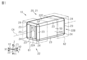
- FIG. 2 is a perspective view of an electronic component.
- FIG. 2 is a cross-sectional view of the XY plane passing through the central axis CA in FIG. 1.
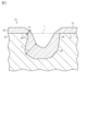
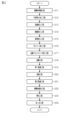
- FIG. FIG. 3 is an enlarged cross-sectional view of a recess and its vicinity. It is a flowchart explaining the manufacturing method of an electronic component. It is an explanatory view explaining a manufacturing method of an electronic component. It is an explanatory view explaining a manufacturing method of an electronic component. It is an explanatory view explaining a manufacturing method of an electronic component. It is an explanatory view explaining a manufacturing method of an electronic component. It is an explanatory view explaining a manufacturing method of an electronic component. It is an explanatory view explaining a manufacturing method of an electronic component. It is an explanatory view explaining a manufacturing method of an electronic component. It is an explanatory view explaining a manufacturing method of an electronic component. It is an explanatory view explaining a manufacturing method of an electronic component. It is an explanatory view explaining a manufacturing method of an electronic
- the electronic component 10 is, for example, a surface-mounted negative temperature coefficient thermistor component mounted on a circuit board or the like. Note that the negative characteristic thermistor component has a characteristic that the resistance value decreases as the temperature increases.
- the electronic component 10 includes an element body 20.
- the element body 20 has a substantially quadrangular prism shape and has a central axis CA.
- the axis extending along the central axis CA will be referred to as a first axis X.
- one of the axes orthogonal to the first axis X is defined as a second axis Y.
- an axis perpendicular to the first axis X and the second axis Y is defined as a third axis Z.
- one of the directions along the first axis X is defined as a first positive direction X1, and among the directions along the first axis X, the opposite direction to the first positive direction X1 is defined as a first negative direction X2.
- one of the directions along the second axis Y is defined as a second positive direction Y1, and the direction opposite to the second positive direction Y1 among the directions along the second axis Y is defined as a second negative direction Y2.
- one of the directions along the third axis Z is defined as a third positive direction Z1, and among the directions along the third axis Z, the direction opposite to the third positive direction Z1 is defined as a third negative direction Z2.
- the outer surface 21 of the element body 20 has six flat surfaces 22.
- the "surface" of the element body 20 herein refers to what can be observed as a surface when the entire element body 20 is observed. That is, even if there are minute irregularities or steps that cannot be seen unless a part of the element body 20 is observed under a microscope or the like, it is expressed as a flat or curved surface.
- the six planes 22 face different directions.
- the six planes 22 are roughly divided into a first end surface 22A facing the first positive direction X1, a second end surface 22B facing the first negative direction X2, and four side surfaces 22C.
- the four side surfaces 22C are a surface facing the third positive direction Z1, a surface facing the third negative direction Z2, a surface facing the second positive direction Y1, and a surface facing the second negative direction Y2.
- the outer surface 21 of the element body 20 has 12 boundary surfaces 23.
- the boundary surface 23 includes a curved surface existing at the boundary between adjacent planes 22. That is, the boundary surface 23 includes, for example, a curved surface formed by rounding the corner formed by the adjacent planes 22.
- the outer surface 21 of the element body 20 has eight spherical corner surfaces 24.
- the corner surface 24 is a boundary between three adjacent planes 22.
- the corner surface 24 includes a curved surface where the three boundary surfaces 23 intersect. That is, the corner surface 24 includes a curved surface formed by, for example, rounding the corner formed by the three adjacent planes 22.
- the surface of a glass film 50 which will be described later, is identified with the outer surface 21 of the element body 20 and is designated by a reference numeral.
- the dimension of the element body 20 in the direction along the first axis X is larger than the dimension in the direction along the third axis Z. Furthermore, the dimension of the element body 20 in the direction along the first axis X is larger than the dimension in the direction along the second axis Y. Further, the material of the element body 20 is a ceramic made by firing a metal oxide containing one or more components selected from Mn, Fe, Ni, Co, Ti, Ba, Al, and Zn.
- the electronic component 10 includes two first internal electrodes 41 and two second internal electrodes 42.
- the first internal electrode 41 and the second internal electrode 42 are embedded inside the element body 20 .
- the material of the first internal electrode 41 is a conductive material.
- the material of the first internal electrode 41 is palladium.
- the material of the second internal electrode 42 is the same as that of the first internal electrode 41.
- the shape of the first internal electrode 41 is a rectangular plate.
- the main surface of the first internal electrode 41 is perpendicular to the second axis Y.
- the shape of the second internal electrode 42 is the same rectangular plate shape as the first internal electrode 41.
- the main surface of the second internal electrode 42 is perpendicular to the second axis Y, similarly to the first internal electrode 41.
- the dimension of the first internal electrode 41 in the direction along the first axis X is smaller than the dimension of the element body 20 in the direction along the first axis X. Further, as shown in FIG. 1, the dimension of the first internal electrode 41 in the direction along the third axis Z is approximately two-thirds of the dimension of the element body 20 in the direction along the third axis Z. The dimensions of the second internal electrode 42 in each direction are the same as those of the first internal electrode 41.
- the first internal electrodes 41 and the second internal electrodes 42 are located alternately in the direction along the second axis Y. That is, the first internal electrode 41, the second internal electrode 42, the first internal electrode 41, and the second internal electrode 42 are arranged in this order from the side surface 22C facing the second positive direction Y1 toward the second negative direction Y2. In this embodiment, the distance between each internal electrode in the direction along the second axis Y is equal.
- the two first internal electrodes 41 and the two second internal electrodes 42 are both located at the center of the element body 20 in the direction along the third axis Z.
- the first internal electrode 41 is located closer to the first positive direction X1.
- the second internal electrode 42 is located closer to the first negative direction X2.
- the end of the first internal electrode 41 on the first positive direction X1 side matches the end of the element body 20 on the first positive direction X1 side.
- the end of the first internal electrode 41 on the first negative direction X2 side is located inside the element body 20 and does not reach the end of the element body 20 on the first negative direction X2 side.
- the end of the second internal electrode 42 on the first negative direction X2 side coincides with the end of the element body 20 on the first negative direction X2 side.
- the end of the second internal electrode 42 on the first positive direction X1 side is located inside the element body 20 and does not reach the end of the element body 20 on the first positive direction X1 side.
- the electronic component 10 includes a glass film 50.
- Glass film 50 covers outer surface 21 of element body 20 .
- the glass film 50 covers the entire area of the outer surface 21 of the element body 20.
- the main material of the glass film 50 is insulating glass. Therefore, the glass film 50 contains silicon dioxide.
- the glass film 50 contains one or more elements selected from alkali metals and alkaline earth metals as additives.
- the glass film 50 contains potassium as an additive.
- the value of "K/Si" which is the ratio of potassium to silicon contained in the glass film 50, is 0.5 atm% or more and 90 atm% or less. Specifically, the ratio of potassium to silicon contained in the glass film 50 is about 30 atm %.
- the electronic component 10 includes a first external electrode 61 and a second external electrode 62.
- the first external electrode 61 includes a first base electrode 61A and a first metal layer 61B.
- the first base electrode 61A is laminated on the glass film 50 on a portion of the outer surface 21 of the element body 20 including the first end surface 22A.
- the first base electrode 61A is a five-sided electrode that covers the first end surface 22A of the element body 20 and a portion of the four side surfaces 22C on the first positive direction X1 side.
- the material of the first base electrode 61A is a mixture of silver and glass.
- the first metal layer 61B covers the first base electrode 61A from the outside. Therefore, the first metal layer 61B is laminated on the first base electrode 61A. Although not shown, the first metal layer 61B has a two-layer structure including a nickel layer and a tin layer in order from the first base electrode 61A side.
- the second external electrode 62 includes a second base electrode 62A and a second metal layer 62B.
- the second base electrode 62A is laminated over the glass film 50 on a portion of the outer surface 21 of the element body 20 that includes the second end surface 22B.
- the second base electrode 62A is a five-sided electrode that covers the second end surface 22B of the element body 20 and a portion of the four side surfaces 22C on the first negative direction X2 side.
- the material of the second base electrode 62A is the same as that of the first external electrode 61, and is a mixture of silver and glass.
- the second metal layer 62B covers the second base electrode 62A from the outside. Therefore, the second metal layer 62B is laminated on the second base electrode 62A. Specifically, the second metal layer 62B has a two-layer structure of a nickel layer and a tin layer, similar to the first metal layer 61B.
- the second external electrode 62 does not reach the first external electrode 61 on the side surface 22C, and is arranged apart from the first external electrode 61 in the direction along the first axis X.
- the first external electrode 61 and the second external electrode 62 are not stacked at the central portion in the direction along the first axis X, and the glass film 50 is exposed.
- the first external electrode 61 and the second external electrode 62 are illustrated by two-dot chain lines.
- the first external electrode 61 and the end of the first internal electrode 41 on the first positive direction X1 side are connected via a first penetration portion 71 that penetrates the glass film 50.
- the first penetrating portion 71 is formed by palladium forming the first internal electrode 41 extending toward the first external electrode 61 during the manufacturing process of the electronic component 10.
- the second external electrode 62 and the end of the second internal electrode 42 on the first negative direction X2 side are connected via a second penetration portion 72 that penetrates the glass film 50.
- the second penetration part 72 is also formed by palladium forming the second internal electrode 42 extending toward the second external electrode 62 during the manufacturing process of the electronic component 10.
- FIG. 2 shows the first internal electrode 41 and the first penetration part 71 as separate members with a boundary, there is actually no clear boundary between them. The same applies to the second penetrating portion 72 in this respect.
- illustration of the first penetration part 71 and the second penetration part 72 is omitted.
- the outer surface 21 of the element body 20 has one or more recesses 25.
- the recess 25 is recessed toward the inside of the element body 20 with respect to the surroundings.
- the glass film 50 described above also covers the recess 25 on the outer surface 21.
- the glass film 50 follows the concave shape of the recess 25 to some extent. That is, the portion of the outer surface 51 of the glass film 50 that covers the recess 25 is recessed toward the element body 20 with respect to the surroundings.
- the opening edge 26 of the recess 25 is defined as follows. First, one recess 25 is viewed in cross section along a plane perpendicular to the outer surface 21. As shown in FIG. Then, on this cross section, a tangent line T that circumscribes both outer surfaces 21 on both sides of the recess 25 is drawn. At this time, the tangent T may partially coincide with the outer surface 21. Among the points of contact between this tangent T and the outer surface 21, the end on the center side of the recess 25 is defined as an opening edge 26.
- the ratio of the minimum thickness TS to the maximum thickness TL of the glass film 50 covering the recess 25 is 0.05 or more and 0.8 or less.
- the thickness of the glass film 50 is calculated as follows. First, a cross section perpendicular to the outer surface 21 of the electronic component 10 is photographed using an electron microscope. Then, in the photographed image, the shortest distance from an arbitrary point on the recess 25 to the outer surface 51 of the glass film 50 is calculated. This is the thickness of the glass film 50 that covers any one point on the recess 25. Then, on the image captured by the electron microscope, the thickness of the glass film 50 covering the recess 25 is measured within the range from one opening edge 26 of the recess 25 to the other opening edge 26.
- the maximum value TL and minimum value TS are specified.
- the maximum value TL is measured at or near the deepest part of the recess 25.
- the minimum value TS is measured at or near the opening edge 26 of the recess 25 .
- the value of "minimum value TS/maximum value TL” is 0.05 or more and 0.8 or less. Specifically, in the example shown in FIG. 3, the value of "minimum value TS/maximum value TL" is approximately 0.24.
- the method for manufacturing the electronic component 10 includes a laminate preparation step S11, an R chamfering step S12, a solvent charging step S13, a catalyst charging step S14, an element charging step S15, and a polymer charging step S15.
- the method includes a step S16 and a metal alkoxide charging step S17.
- the method for manufacturing the electronic component 10 also includes a film forming step S18, a first drying step S19, a dipping step S20, a second drying step S21, a conductor coating step S22, a curing step S23, and a plating step S24. It also has the following.
- a laminate which is the element body 20 without the boundary surface 23 and the corner surface 24 is prepared. That is, the laminate is in a state before R-chamfering and is in the shape of a rectangular parallelepiped with six planes 22.
- a plurality of ceramic sheets that will become the element body 20 are prepared. The sheet is in the form of a thin plate. A conductive paste that will become the first internal electrode 41 is laminated on the sheet. A ceramic sheet that will become the element body 20 is laminated on the lamination paste. A conductive paste that will become the second internal electrode 42 is laminated on the sheet. In this way, the ceramic sheet and the conductive paste are laminated.
- an unfired laminate is formed. Thereafter, a laminate is prepared by firing the unfired laminate at a high temperature.
- an R chamfering step S12 is performed.
- a boundary surface 23 and a corner surface 24 are formed on the laminate prepared in the laminate preparation step S11.
- the corners of the laminate are rounded to form a curved boundary surface 23 and a curved corner surface 24 .
- the element body 20 is formed.
- recesses 25 may be formed on the outer surface 21 of the elements 20.
- the unevenness of that portion remains as a recess 25 even after barrel-polishing.
- the outer surface 21 of the element body 20 is not polished sufficiently by barrel polishing, the unevenness on the outer surface 21 of the element body 20 that was formed before barrel polishing is not completely polished and remains as a recess 25.
- I do I do.
- a solvent injection step S13 is performed.
- 2-propanol is charged as the solvent 82 into the reaction vessel 81.
- a catalyst charging step S14 is performed.
- FIG. 6 in the catalyst charging step S14, first, stirring of the solvent 82 in the reaction vessel 81 is started. Then, aqueous ammonia is poured into the reaction vessel 81 as an aqueous solution 83 containing a catalyst.
- the catalyst in this embodiment is a hydroxide ion, and functions as a catalyst that promotes the hydrolysis of metal alkoxide 85, which will be described later.
- an element loading step S15 is performed. As shown in FIG. 7, in the element loading step S15, the plurality of elements 20 previously formed in the R-chamfering process S12 as described above are charged into the reaction container 81.
- a polymer charging step S16 is performed. As shown in FIG. 8, in the polymer charging step S16, polyvinylpyrrolidone is charged as the polymer 84 into the reaction container 81. As a result, the polymer 84 introduced into the reaction container 81 is adsorbed onto the outer surface 21 of the element body 20 .
- a metal alkoxide charging step S17 is performed.
- liquid tetraethyl orthosilicate is charged as the metal alkoxide 85 into the reaction vessel 81.
- tetraethyl orthosilicate is sometimes called tetraethoxysilane.
- the amount of metal alkoxide 85 introduced in the metal alkoxide introduction step S17 is calculated based on the area of the outer surface 21 of the element body 20 introduced in the element body introduction step S15. Specifically, it is calculated by multiplying the amount of metal alkoxide 85 per element body 20 necessary to form the glass film 50 covering the outer surface 21 of the element body 20 by the number of element bodies 20. .
- a film forming step S18 is performed.
- the stirring of the solvent 82 started in the above-mentioned solvent charging step S13 is continued for a predetermined period of time after the metal alkoxide 85 is charged into the reaction vessel 81 in the metal alkoxide charging step S17.
- the metal alkoxide 85 is hydrolyzed by the hydroxide ion that is the catalyst.
- the hydrolyzed metal alkoxide 85 adheres to the surface of the element body 20 .
- the metal alkoxides 85 adhering to the surface of the element body 20 are dehydrated and condensed to form the glass film 50.
- a sol-like glass film 50 is formed by a liquid phase reaction within the reaction vessel 81.
- a first drying step S19 is performed.
- the element body 20 is taken out from the reaction container 81 and dried.
- the sol-like glass film 50 is dried and becomes a gel-like glass film 50.
- a dipping step S20 is performed.
- at least one element selected from alkali metals and alkaline earth metals is added as an additive to a reaction container 86 different from the reaction container 81 used up to the film forming step S18.
- a solution 87 containing is an aqueous solution containing a potassium oxide precursor.
- the element body 20 having the gel-like glass film 50 is immersed in the solution 87. As a result, the solution 87 adheres to the surface of the glass film 50.
- a second drying step S21 is performed.
- the element body 20 immersed in the solution 87 in the dipping step S20 is taken out from the reaction container 86 and dried.
- the water in the solution 87 adhering to the surface of the glass film 50 evaporates.
- the potassium oxide precursor contained in the solution 87 is deposited on the outer surface 51 of the glass film 50.
- a conductor coating step S22 is performed.
- two parts of the surface of the glass film 50 are formed: a part including a part covering the first end face 22A of the element body 20, and a part including a part covering the second end face 22B of the element body 20.
- a curing step S23 is performed. Specifically, in the curing step S23, the glass film 50 and the element body 20 coated with the conductive paste are heated. As a result, the precipitated potassium oxide precursor becomes potassium oxide. Potassium oxide diffuses into the glass film 50 covering the outer surface 21 of the element body 20 . Then, as water and polymer 84 evaporate from gel-like glass film 50, glass film 50 covering outer surface 21 of element body 20 is fired and hardened. Further, in the curing step S23, the conductor paste applied in the conductor application step S22 is fired, thereby forming the first base electrode 61A and the second base electrode 62A.
- the first penetrating portion 71 extends through the glass film 50 from the first internal electrode 41 toward the first base electrode 61A, thereby connecting the first internal electrode 41 and the first base electrode 61A.
- the second through portion 72 that connects the second internal electrode 42 and the second base electrode 62A.
- a plating step S24 is performed. Electroplating is performed on the first base electrode 61A and the second base electrode 62A. As a result, a first metal layer 61B is formed on the surface of the first base electrode 61A. Further, a second metal layer 62B is formed on the surface of the second base electrode 62A. Although not shown, the first metal layer 61B and the second metal layer 62B are electroplated with two types of metal, nickel and tin, so that they have a two-layer structure. In this way, electronic component 10 is formed.
- the ratio of the minimum value TS to the maximum value TL of the thickness of the glass film 50 covering the recess 25 is 0.05 or more and 0.8 or less.
- the glass film 50 covering the recess 25 has a maximum thickness at a portion covering the vicinity of the deepest part of the recess 25 .
- the glass film 50 covering the recess 25 has a minimum thickness at a portion covering the vicinity of the opening edge 26 of the recess 25 . That is, the thickness of the glass film 50 covering the recess 25 does not change rapidly from the deepest part of the recess 25 to the opening edge 26 of the recess 25 . Therefore, occurrence of cracks or the like in the glass film 50 covering the recess 25 can be prevented.
- the softening point of the glass film 50 is lower than when the glass film 50 does not contain an alkali metal or an alkaline earth metal. Therefore, the glass melted in the curing step S23 tends to reach the inside of the recess 25. As a result, a portion of the recess 25 can be filled with the glass film 50, and the flatness of the outer surface 51 of the glass film 50 is increased.
- the glass film 50 contains an alkali metal or an alkaline earth metal, and the ratio of the alkali metal or the alkaline earth metal to Si contained in the glass film 50 is 0.5 atm% or more and 90 atm%. It is as follows. By including an alkali metal or an alkaline earth metal in the glass film 50 within the range of this ratio, the ratio of the minimum value TS to the maximum value TL of the thickness of the glass film 50 covering the recess 25 is set to be 0.05 or more and 0.05 or more. Easy to control to 8 or less.
- the dipping step S20 and the second drying step S21 are performed to form a glass containing an alkali metal or an alkaline earth metal as an additive.
- a film 50 can be formed.
- the dipping step S20 and the second drying step S21 can be easily performed without requiring any special equipment or the like. Therefore, the manufacturing method of the above embodiment can be realized without major changes from the conventional manufacturing process.
- the electronic component 10 is not limited to a negative characteristic thermistor component.
- the electronic component 10 may be a thermistor component with a non-negative characteristic, a multilayer capacitor component, or an inductor component.
- the material of the element body 20 is not limited to the example of the above embodiment.
- the material of the element body 20 may be a composite body of resin and metal powder.
- the shape of the element body 20 is not limited to the example of the above embodiment.
- the element body 20 may have a polygonal columnar shape other than a quadrangular columnar shape having the central axis CA.
- the element body 20 may be a core of a wire-wound inductor component.
- the core may have a so-called drum core shape.
- the core may include a columnar winding core and a flange provided at each end of the winding core.
- the outer surface 21 of the element body 20 does not need to have the boundary surface 23 and the corner surface 24.
- the boundary surface 23 and the corner surface 24 may not exist.
- the shapes of the first internal electrode 41 and the second internal electrode 42 are not limited as long as they can ensure electrical continuity with the corresponding first external electrode 61 and second external electrode 62. Moreover, the number of the first internal electrodes 41 and the second internal electrodes 42 does not matter, and the number of internal electrodes may be one or three or more.
- the configuration of the first external electrode 61 is not limited to the example of the above embodiment.
- the first external electrode 61 may be composed only of the first base electrode 61A, and the first metal layer 61B may not have a two-layer structure. The same applies to the second external electrode 62 in this respect.
- the combination of materials for the first internal electrode 41 and the first base electrode 61A is not limited to the combination of palladium and silver.
- it may be a combination of copper and nickel, copper and silver, silver and gold, nickel and cobalt, or nickel and gold.
- one may be silver and the other may be a combination of silver and palladium.
- one may be a combination of palladium and the other of silver and palladium, or one may be copper and the other a combination of silver and palladium.
- one may be gold and the other may be a combination of silver and palladium.
- the first internal electrode 41 may be processed to be exposed before the external electrode forming step. For example, a portion of the glass film 50 may be physically removed by polishing the first end surface 22A side of the element body 20. Thereafter, by performing a base electrode forming step, the first internal electrode 41 and the first base electrode 61A can be connected. For example, after forming the first base electrode 61A, the glass film 50 may be formed including the surface of the first base electrode 61A, and the glass film 50 covering the surface of the first base electrode 61A may be removed. The same applies to the combination of materials for the second internal electrode 42 and the second base electrode 62A.
- the arrangement location of the first external electrode 61 is not limited to the example of the above embodiment.
- the first external electrode 61 may be arranged only on the first end surface 22A and one side surface 22C.
- the glass film 50 does not need to cover the entire area of the outer surface 21 of the element body 20.
- the range covered by the glass film 50 may be changed as appropriate in accordance with the shape of the element body 20, the positions of the first external electrode 61 and the second external electrode 62, and the like.
- the glass in the glass film 50 may diffuse into the glass in the first base electrode 61A, so that the two may be integrated.
- the glass film 50 can prevent cracks from occurring if the ratio of the minimum thickness TS to the maximum thickness TL of the glass film 50 covering the recess 25 is 0.05 or more and 0.8 or less. Therefore, the glass film 50 does not need to contain one or more elements selected from alkali metals and alkaline earth metals as additives.
- the ratio of the additive to Si contained in the glass film 50 is less than 0.5 atm%, Alternatively, it may be greater than 90 atm%.
- glass is not limited to silicon dioxide, but may be a multi-component oxide containing Si, such as B-Si, Si-Zn, Zr-Si, or Al-Si oxides. Good too. Further, the glass may be a multi-component oxide containing an alkali metal and Si, such as an Al--Si, Na--Si, or Li--Si oxide. Further, the glass may be a multi-component oxide containing an alkaline earth metal and Si, such as Mg--Si, Ca--Si, Ba--Si, or Sr--Si. The glass may not contain Si or may be a mixture thereof.
- the material of the glass film 50 may include, in addition to glass, a surface treatment agent such as a pigment, a silicone flame retardant, a silane coupling agent, a titanate coupling agent, or an antistatic agent. More specifically, in addition to glass, the glass film 50 may contain additives such as organic acid salts, oxides, inorganic salts, organic salts, and other fine particles and nanoparticles of metal oxides. . Furthermore, the additives contained in the solution 87 are not limited to the potassium oxide precursor.
- organic acid salts include salts of oxoacids such as soda ash, sodium carbonate, sodium hydrogen carbonate, sodium percarbonate, sodium sulfite, sodium hydrogen sulfite, sodium sulfate, sodium thiosulfate, sodium nitrate, and sodium sulfite, and sodium fluoride. , sodium chloride, sodium bromide, and sodium iodide.
- Examples of the oxide include sodium peroxide, and examples of the hydroxide include sodium hydroxide.
- examples of inorganic salts include sodium hydride, sodium sulfide, sodium hydrogen sulfide, sodium silicate, trisodium phosphate, sodium borate, sodium borohydride, sodium cyanide, sodium cyanate, and sodium tetrachloroaurate. .
- examples of inorganic salts include calcium peroxide, calcium hydroxide, calcium fluoride, calcium chloride, calcium bromide, calcium iodide, calcium hydride, calcium carbide, and calcium phosphide.
- Additives include calcium carbonate, calcium hydrogen carbonate, calcium nitrate, calcium sulfate, calcium sulfite, calcium silicate, calcium phosphate, calcium pyrophosphate, calcium hypochlorite, calcium chlorate, calcium perchlorate, calcium bromate, and iodine.
- Oxoacid salts such as calcium acid, calcium arsenite, calcium chromate, calcium tungstate, calcium molybdate, calcium magnesium carbonate, and hydroxyapatite may also be used.
- additives include calcium acetate, calcium gluconate, calcium citrate, calcium malate, calcium lactate, calcium benzoate, calcium stearate, and calcium aspartate.
- additives include lithium carbonate, lithium chloride, lithium titanate, lithium nitride, lithium peroxide, lithium citrate, lithium fluoride, lithium hexafluorophosphate, lithium acetate, lithium iodide, and lithium hypochlorite.
- the additive may be boron triiodide, sodium cyanoborohydride, sodium borohydride, tetrafluoroboric acid, triethylborane, borax, or boric acid.
- additives include barium sulfite, barium chloride, barium chlorate, barium perchlorate, barium peroxide, barium chromate, barium acetate, barium cyanide, barium bromide, barium oxalate, barium nitrate, and hydroxide. It may be barium, barium hydride, barium carbonate, barium iodide, barium sulfide, or barium sulfate. Other additives may include sodium acetate and sodium citrate.
- the additive may be fine particles or nanoparticles of metal oxides.
- metal oxides include sodium oxide, calcium oxide, lithium oxide, boron oxide, barium oxide, silicon oxide, and titanium oxide. , zircon oxide, aluminum oxide, zinc oxide, and magnesium oxide.
- the potassium oxide precursor is, for example, potassium arsenide, potassium bromide, potassium carbide, potassium chloride, potassium fluoride, potassium hydride, potassium iodide, potassium triiodide, potassium azide, potassium nitride.
- potassium sulfate potassium acetate
- potassium gold(I) cyanide potassium hexanitrocobaltate(III), hexacyano Potassium ferrate (III), potassium hexacyano
- Metal alkoxide 85 is, for example, sodium methoxide, sodium ethoxide, calcium diethoxide, lithium isopropoxide, lithium ethoxide, lithium tert-butoxide, lithium methoxide, boron alkoxide, potassium t-butoxide, tetraethyl orthosilicate, Allyltrimethoxysilane, isobutyl(trimethoxy)silane, tetrapropyl orthosilicate, tetramethyl orthosilicate, [3-(diethylamino)propyl]trimethoxysilane, triethoxy(octyl)silane, triethoxyvinylsilane, triethoxyphenylsilane, trimethoxy Phenylsilane, trimethoxymethylsilane, butyltrichlorosilane, n-propyltriethoxysilane, methyltrichlorosilane, dime
- a metal complex or acetate which is a precursor of the metal alkoxide 85, may be used instead of the metal alkoxide 85.
- a metal complex or acetate which is a metal alkoxide precursor, may be charged.
- metal complexes include lithium acetylacetonate, titanium (IV) oxyacetylacetonate, titanium diisopropoxide bis(acetylacetonate), zirconium (IV) trifluoroacetylacetonate, and zirconium (IV) acetylacetonate.
- examples of the acetate include zirconium acetate, zirconium (IV) acetic acid hydroxide, and basic aluminum acetate.
- the solvent 82 introduced in the solvent injection step S13 is not limited to the example of the above embodiment, and may be any liquid that can appropriately disperse the metal alkoxide 85.
- the solvent charging step S13 may be performed after the catalyst charging step S14 or the element charging step S15.
- the solvent charging step S13 may be performed before at least one of the metal alkoxide charging step S17 and the catalyst charging step S14.
- the solvent injection step S13 may be omitted. In this case, for example, if the amount of water contained in the aqueous solution 83 containing the catalyst is correspondingly large, the metal alkoxide 85 reacts in the liquid phase.
- the aqueous solution 83 containing the catalyst may be mixed with an organic solvent as the solvent 82 and then introduced.
- the aqueous solution 83 containing the catalyst is ammonia water, and the catalyst is hydroxide ion, but the catalyst is not limited to this. If it is a basic aqueous solution, it can catalyze the hydrolysis of the metal alkoxide 85, similar to the aqueous ammonia in the above embodiment, and even if it is an acidic aqueous solution, it can catalyze the hydrolysis of the metal alkoxide 85. Furthermore, even if the aqueous solution is neutral, it is sufficient if the aqueous solution contains ions that can catalyze hydrolysis.
- the catalyst is introduced as an aqueous solution 83 containing the catalyst, but a solid compound containing the catalyst and water may be separately introduced into the reaction vessel 81, and in this case, It can be considered that the catalyst was introduced into the reaction container 81 because the catalyst was generated in the reaction container 81.
- a solid compound containing a catalyst may be put into the reaction vessel 81, and moisture in the air may be used as the water necessary for hydrolysis.
- the element body charging step S15 may be performed before the catalyst charging step S14. Further, when the element body charging step S15 is performed before the catalyst charging step S14, the metal alkoxide charging step S17 may be performed before the catalyst charging step S14 or the element body charging step S15. The element body charging step S15 may be performed before at least one of the metal alkoxide charging step S17 and the catalyst charging step S14.
- a solution containing a precursor for producing the metal alkoxide 85 may be charged.
- the metal alkoxide 85 may be generated inside the reaction vessel 81 without having to generate the metal alkoxide 85 outside the reaction vessel 81 and then charging it into the reaction vessel 81.
- metal alkoxide 85 is produced by reacting a metal salt with an alcohol. Therefore, the metal alkoxide 85 is also introduced into the reaction container 81 when the metal salt and alcohol, which are metal alkoxide precursors, are introduced into the reaction container 81 and the metal alkoxide 85 is generated by the reaction. It can be considered that
- the metal alkoxide 85 is not limited to tetraethyl orthosilicate.
- the metal contained in the metal alkoxide 85 may be titanium, zirconium, aluminum, or the like. Note that when the metal contained in the metal alkoxide 85 is silicon, the reaction rate is slower than that of other metals, so the reaction rate of the metal alkoxide 85 can be easily controlled to be constant.
- the alkoxy group of metal alkoxide 85 a methoxy group, a propoxy group, etc. may be used, or a functional group such as a long-chain alkyl group or an epoxy group may be modified like a coupling agent.
- the number of coordinations to the metal contained in the metal alkoxide 85 is not limited to four coordinations, but may be three coordinations or two coordinations.
- the reaction container 86 different from the reaction container 81 was used in the immersion step S20. However, if the solution used up to the film-forming step S18 in the reaction container 81 is removed and the solution 87 is newly put into the reaction container 81, the reaction container 81 used up to the film-forming step S18 can be used. Good too.
- the solution 87 only needs to adhere to the glass film 50 covering the outer surface 21 of the element body 20, and the entire element body 20 does not have to be immersed in the solution 87 in the reaction container 86.
- the solution 87 may be applied only to the portion of the outer surface 21 of the element body 20 that is covered with the glass film 50.
- the curing step S23 is not limited to the step of curing the glass film 50 and the conductive paste at the same time.
- the conductive paste is a material that can be cured by ultraviolet irradiation
- a heating process may be performed as a curing process for curing the glass film 50
- ultraviolet irradiation may be performed as a curing process for the conductive paste.
Landscapes
- Engineering & Computer Science (AREA)
- Microelectronics & Electronic Packaging (AREA)
- Manufacturing & Machinery (AREA)
- Physics & Mathematics (AREA)
- Electromagnetism (AREA)
- Fixed Capacitors And Capacitor Manufacturing Machines (AREA)
Priority Applications (2)
| Application Number | Priority Date | Filing Date | Title |
|---|---|---|---|
| JP2024543822A JPWO2024048037A1 (https=) | 2022-08-31 | 2023-06-23 | |
| US18/608,018 US20240221981A1 (en) | 2022-08-31 | 2024-03-18 | Electronic component and film forming method |
Applications Claiming Priority (2)
| Application Number | Priority Date | Filing Date | Title |
|---|---|---|---|
| JP2022137882 | 2022-08-31 | ||
| JP2022-137882 | 2022-08-31 |
Related Child Applications (1)
| Application Number | Title | Priority Date | Filing Date |
|---|---|---|---|
| US18/608,018 Continuation US20240221981A1 (en) | 2022-08-31 | 2024-03-18 | Electronic component and film forming method |
Publications (1)
| Publication Number | Publication Date |
|---|---|
| WO2024048037A1 true WO2024048037A1 (ja) | 2024-03-07 |
Family
ID=90099417
Family Applications (1)
| Application Number | Title | Priority Date | Filing Date |
|---|---|---|---|
| PCT/JP2023/023393 Ceased WO2024048037A1 (ja) | 2022-08-31 | 2023-06-23 | 電子部品及び成膜方法 |
Country Status (3)
| Country | Link |
|---|---|
| US (1) | US20240221981A1 (https=) |
| JP (1) | JPWO2024048037A1 (https=) |
| WO (1) | WO2024048037A1 (https=) |
Citations (4)
| Publication number | Priority date | Publication date | Assignee | Title |
|---|---|---|---|---|
| JPH05251210A (ja) * | 1991-12-20 | 1993-09-28 | Mitsubishi Materials Corp | 導電性チップ型セラミック素子及びその製造方法 |
| JP2020136570A (ja) * | 2019-02-22 | 2020-08-31 | 三菱マテリアル株式会社 | サーミスタの製造方法 |
| JP2021019002A (ja) * | 2019-07-17 | 2021-02-15 | 三菱マテリアル株式会社 | 電子部品の製造方法 |
| JP2021027163A (ja) * | 2019-08-05 | 2021-02-22 | 三菱マテリアル株式会社 | 保護膜付きサーミスタおよびその製造方法 |
-
2023
- 2023-06-23 WO PCT/JP2023/023393 patent/WO2024048037A1/ja not_active Ceased
- 2023-06-23 JP JP2024543822A patent/JPWO2024048037A1/ja active Pending
-
2024
- 2024-03-18 US US18/608,018 patent/US20240221981A1/en active Pending
Patent Citations (4)
| Publication number | Priority date | Publication date | Assignee | Title |
|---|---|---|---|---|
| JPH05251210A (ja) * | 1991-12-20 | 1993-09-28 | Mitsubishi Materials Corp | 導電性チップ型セラミック素子及びその製造方法 |
| JP2020136570A (ja) * | 2019-02-22 | 2020-08-31 | 三菱マテリアル株式会社 | サーミスタの製造方法 |
| JP2021019002A (ja) * | 2019-07-17 | 2021-02-15 | 三菱マテリアル株式会社 | 電子部品の製造方法 |
| JP2021027163A (ja) * | 2019-08-05 | 2021-02-22 | 三菱マテリアル株式会社 | 保護膜付きサーミスタおよびその製造方法 |
Also Published As
| Publication number | Publication date |
|---|---|
| US20240221981A1 (en) | 2024-07-04 |
| JPWO2024048037A1 (https=) | 2024-03-07 |
Similar Documents
| Publication | Publication Date | Title |
|---|---|---|
| US12476049B2 (en) | Electronic component and method for manufacturing the same | |
| US20240021347A1 (en) | Electronic component | |
| US12557212B2 (en) | Electronic component | |
| US20250266189A1 (en) | Protective glass film | |
| US20240021346A1 (en) | Electronic component | |
| JP7156520B2 (ja) | 表面改質ガラス、電子部品、及び、ケイ酸塩皮膜の形成方法 | |
| US12308174B2 (en) | Electronic component | |
| US20240304363A1 (en) | Electronic component | |
| WO2024048037A1 (ja) | 電子部品及び成膜方法 | |
| US20250118462A1 (en) | Electronic component | |
| JP7582508B2 (ja) | 電子部品 | |
| WO2025004432A1 (ja) | 電子部品 | |
| WO2024029252A1 (ja) | 電子部品 | |
| CN117897785A (zh) | 电子部件 | |
| WO2025249191A1 (ja) | 電子部品 | |
| WO2025249192A1 (ja) | 電子部品 | |
| WO2025169709A1 (ja) | 電子部品 | |
| US20250118461A1 (en) | Electronic component and method for manufacturing electronic component | |
| WO2025089298A1 (ja) | 電子部品、保護膜の成膜方法、及び電子部品の製造方法 |
Legal Events
| Date | Code | Title | Description |
|---|---|---|---|
| 121 | Ep: the epo has been informed by wipo that ep was designated in this application |
Ref document number: 23859807 Country of ref document: EP Kind code of ref document: A1 |
|
| WWE | Wipo information: entry into national phase |
Ref document number: 2024543822 Country of ref document: JP |
|
| NENP | Non-entry into the national phase |
Ref country code: DE |
|
| 122 | Ep: pct application non-entry in european phase |
Ref document number: 23859807 Country of ref document: EP Kind code of ref document: A1 |