WO2024043221A1 - 感光性表面処理剤、パターン形成用基板、積層体、トランジスタ、パターン形成方法及びトランジスタの製造方法 - Google Patents
感光性表面処理剤、パターン形成用基板、積層体、トランジスタ、パターン形成方法及びトランジスタの製造方法 Download PDFInfo
- Publication number
- WO2024043221A1 WO2024043221A1 PCT/JP2023/030083 JP2023030083W WO2024043221A1 WO 2024043221 A1 WO2024043221 A1 WO 2024043221A1 JP 2023030083 W JP2023030083 W JP 2023030083W WO 2024043221 A1 WO2024043221 A1 WO 2024043221A1
- Authority
- WO
- WIPO (PCT)
- Prior art keywords
- resin film
- surface treatment
- treatment agent
- photosensitive
- photosensitive surface
- Prior art date
- Legal status (The legal status is an assumption and is not a legal conclusion. Google has not performed a legal analysis and makes no representation as to the accuracy of the status listed.)
- Ceased
Links
Images


Classifications
-
- G—PHYSICS
- G03—PHOTOGRAPHY; CINEMATOGRAPHY; ANALOGOUS TECHNIQUES USING WAVES OTHER THAN OPTICAL WAVES; ELECTROGRAPHY; HOLOGRAPHY
- G03F—PHOTOMECHANICAL PRODUCTION OF TEXTURED OR PATTERNED SURFACES, e.g. FOR PRINTING, FOR PROCESSING OF SEMICONDUCTOR DEVICES; MATERIALS THEREFOR; ORIGINALS THEREFOR; APPARATUS SPECIALLY ADAPTED THEREFOR
- G03F7/00—Photomechanical, e.g. photolithographic, production of textured or patterned surfaces, e.g. printing surfaces; Materials therefor, e.g. comprising photoresists; Apparatus specially adapted therefor
- G03F7/004—Photosensitive materials
- G03F7/075—Silicon-containing compounds
- G03F7/0755—Non-macromolecular compounds containing Si-O, Si-C or Si-N bonds
-
- H—ELECTRICITY
- H10—SEMICONDUCTOR DEVICES; ELECTRIC SOLID-STATE DEVICES NOT OTHERWISE PROVIDED FOR
- H10P—GENERIC PROCESSES OR APPARATUS FOR THE MANUFACTURE OR TREATMENT OF DEVICES COVERED BY CLASS H10
- H10P14/00—Formation of materials, e.g. in the shape of layers or pillars
- H10P14/40—Formation of materials, e.g. in the shape of layers or pillars of conductive or resistive materials
- H10P14/46—Formation of materials, e.g. in the shape of layers or pillars of conductive or resistive materials using a liquid
-
- C—CHEMISTRY; METALLURGY
- C07—ORGANIC CHEMISTRY
- C07F—ACYCLIC, CARBOCYCLIC OR HETEROCYCLIC COMPOUNDS CONTAINING ELEMENTS OTHER THAN CARBON, HYDROGEN, HALOGEN, OXYGEN, NITROGEN, SULFUR, SELENIUM OR TELLURIUM
- C07F7/00—Compounds containing elements of Groups 4 or 14 of the Periodic Table
- C07F7/02—Silicon compounds
- C07F7/08—Compounds having one or more C—Si linkages
- C07F7/18—Compounds having one or more C—Si linkages as well as one or more C—O—Si linkages
-
- C—CHEMISTRY; METALLURGY
- C23—COATING METALLIC MATERIAL; COATING MATERIAL WITH METALLIC MATERIAL; CHEMICAL SURFACE TREATMENT; DIFFUSION TREATMENT OF METALLIC MATERIAL; COATING BY VACUUM EVAPORATION, BY SPUTTERING, BY ION IMPLANTATION OR BY CHEMICAL VAPOUR DEPOSITION, IN GENERAL; INHIBITING CORROSION OF METALLIC MATERIAL OR INCRUSTATION IN GENERAL
- C23C—COATING METALLIC MATERIAL; COATING MATERIAL WITH METALLIC MATERIAL; SURFACE TREATMENT OF METALLIC MATERIAL BY DIFFUSION INTO THE SURFACE, BY CHEMICAL CONVERSION OR SUBSTITUTION; COATING BY VACUUM EVAPORATION, BY SPUTTERING, BY ION IMPLANTATION OR BY CHEMICAL VAPOUR DEPOSITION, IN GENERAL
- C23C18/00—Chemical coating by decomposition of either liquid compounds or solutions of the coating forming compounds, without leaving reaction products of surface material in the coating; Contact plating
- C23C18/16—Chemical coating by decomposition of either liquid compounds or solutions of the coating forming compounds, without leaving reaction products of surface material in the coating; Contact plating by reduction or substitution, e.g. electroless plating
- C23C18/1601—Process or apparatus
- C23C18/1603—Process or apparatus coating on selected surface areas
- C23C18/1607—Process or apparatus coating on selected surface areas by direct patterning
- C23C18/1608—Process or apparatus coating on selected surface areas by direct patterning from pretreatment step, i.e. selective pre-treatment
-
- G—PHYSICS
- G03—PHOTOGRAPHY; CINEMATOGRAPHY; ANALOGOUS TECHNIQUES USING WAVES OTHER THAN OPTICAL WAVES; ELECTROGRAPHY; HOLOGRAPHY
- G03C—PHOTOSENSITIVE MATERIALS FOR PHOTOGRAPHIC PURPOSES; PHOTOGRAPHIC PROCESSES, e.g. CINE, X-RAY, COLOUR, STEREO-PHOTOGRAPHIC PROCESSES; AUXILIARY PROCESSES IN PHOTOGRAPHY
- G03C1/00—Photosensitive materials
- G03C1/72—Photosensitive compositions not covered by the groups G03C1/005 - G03C1/705
-
- G—PHYSICS
- G03—PHOTOGRAPHY; CINEMATOGRAPHY; ANALOGOUS TECHNIQUES USING WAVES OTHER THAN OPTICAL WAVES; ELECTROGRAPHY; HOLOGRAPHY
- G03F—PHOTOMECHANICAL PRODUCTION OF TEXTURED OR PATTERNED SURFACES, e.g. FOR PRINTING, FOR PROCESSING OF SEMICONDUCTOR DEVICES; MATERIALS THEREFOR; ORIGINALS THEREFOR; APPARATUS SPECIALLY ADAPTED THEREFOR
- G03F7/00—Photomechanical, e.g. photolithographic, production of textured or patterned surfaces, e.g. printing surfaces; Materials therefor, e.g. comprising photoresists; Apparatus specially adapted therefor
- G03F7/004—Photosensitive materials
- G03F7/075—Silicon-containing compounds
- G03F7/0754—Non-macromolecular compounds containing silicon-to-silicon bonds
-
- G—PHYSICS
- G03—PHOTOGRAPHY; CINEMATOGRAPHY; ANALOGOUS TECHNIQUES USING WAVES OTHER THAN OPTICAL WAVES; ELECTROGRAPHY; HOLOGRAPHY
- G03F—PHOTOMECHANICAL PRODUCTION OF TEXTURED OR PATTERNED SURFACES, e.g. FOR PRINTING, FOR PROCESSING OF SEMICONDUCTOR DEVICES; MATERIALS THEREFOR; ORIGINALS THEREFOR; APPARATUS SPECIALLY ADAPTED THEREFOR
- G03F7/00—Photomechanical, e.g. photolithographic, production of textured or patterned surfaces, e.g. printing surfaces; Materials therefor, e.g. comprising photoresists; Apparatus specially adapted therefor
- G03F7/20—Exposure; Apparatus therefor
-
- G—PHYSICS
- G03—PHOTOGRAPHY; CINEMATOGRAPHY; ANALOGOUS TECHNIQUES USING WAVES OTHER THAN OPTICAL WAVES; ELECTROGRAPHY; HOLOGRAPHY
- G03F—PHOTOMECHANICAL PRODUCTION OF TEXTURED OR PATTERNED SURFACES, e.g. FOR PRINTING, FOR PROCESSING OF SEMICONDUCTOR DEVICES; MATERIALS THEREFOR; ORIGINALS THEREFOR; APPARATUS SPECIALLY ADAPTED THEREFOR
- G03F7/00—Photomechanical, e.g. photolithographic, production of textured or patterned surfaces, e.g. printing surfaces; Materials therefor, e.g. comprising photoresists; Apparatus specially adapted therefor
- G03F7/26—Processing photosensitive materials; Apparatus therefor
- G03F7/30—Imagewise removal using liquid means
- G03F7/32—Liquid compositions therefor, e.g. developers
- G03F7/322—Aqueous alkaline compositions
-
- G—PHYSICS
- G03—PHOTOGRAPHY; CINEMATOGRAPHY; ANALOGOUS TECHNIQUES USING WAVES OTHER THAN OPTICAL WAVES; ELECTROGRAPHY; HOLOGRAPHY
- G03F—PHOTOMECHANICAL PRODUCTION OF TEXTURED OR PATTERNED SURFACES, e.g. FOR PRINTING, FOR PROCESSING OF SEMICONDUCTOR DEVICES; MATERIALS THEREFOR; ORIGINALS THEREFOR; APPARATUS SPECIALLY ADAPTED THEREFOR
- G03F7/00—Photomechanical, e.g. photolithographic, production of textured or patterned surfaces, e.g. printing surfaces; Materials therefor, e.g. comprising photoresists; Apparatus specially adapted therefor
- G03F7/26—Processing photosensitive materials; Apparatus therefor
- G03F7/38—Treatment before imagewise removal, e.g. prebaking
-
- G—PHYSICS
- G03—PHOTOGRAPHY; CINEMATOGRAPHY; ANALOGOUS TECHNIQUES USING WAVES OTHER THAN OPTICAL WAVES; ELECTROGRAPHY; HOLOGRAPHY
- G03F—PHOTOMECHANICAL PRODUCTION OF TEXTURED OR PATTERNED SURFACES, e.g. FOR PRINTING, FOR PROCESSING OF SEMICONDUCTOR DEVICES; MATERIALS THEREFOR; ORIGINALS THEREFOR; APPARATUS SPECIALLY ADAPTED THEREFOR
- G03F7/00—Photomechanical, e.g. photolithographic, production of textured or patterned surfaces, e.g. printing surfaces; Materials therefor, e.g. comprising photoresists; Apparatus specially adapted therefor
- G03F7/26—Processing photosensitive materials; Apparatus therefor
- G03F7/40—Treatment after imagewise removal, e.g. baking
-
- H—ELECTRICITY
- H10—SEMICONDUCTOR DEVICES; ELECTRIC SOLID-STATE DEVICES NOT OTHERWISE PROVIDED FOR
- H10D—INORGANIC ELECTRIC SEMICONDUCTOR DEVICES
- H10D30/00—Field-effect transistors [FET]
- H10D30/01—Manufacture or treatment
- H10D30/021—Manufacture or treatment of FETs having insulated gates [IGFET]
-
- H—ELECTRICITY
- H10—SEMICONDUCTOR DEVICES; ELECTRIC SOLID-STATE DEVICES NOT OTHERWISE PROVIDED FOR
- H10D—INORGANIC ELECTRIC SEMICONDUCTOR DEVICES
- H10D30/00—Field-effect transistors [FET]
- H10D30/60—Insulated-gate field-effect transistors [IGFET]
- H10D30/67—Thin-film transistors [TFT]
-
- H—ELECTRICITY
- H10—SEMICONDUCTOR DEVICES; ELECTRIC SOLID-STATE DEVICES NOT OTHERWISE PROVIDED FOR
- H10D—INORGANIC ELECTRIC SEMICONDUCTOR DEVICES
- H10D64/00—Electrodes of devices having potential barriers
- H10D64/01—Manufacture or treatment
-
- H—ELECTRICITY
- H10—SEMICONDUCTOR DEVICES; ELECTRIC SOLID-STATE DEVICES NOT OTHERWISE PROVIDED FOR
- H10P—GENERIC PROCESSES OR APPARATUS FOR THE MANUFACTURE OR TREATMENT OF DEVICES COVERED BY CLASS H10
- H10P76/00—Manufacture or treatment of masks on semiconductor bodies, e.g. by lithography or photolithography
- H10P76/20—Manufacture or treatment of masks on semiconductor bodies, e.g. by lithography or photolithography of masks comprising organic materials
- H10P76/204—Manufacture or treatment of masks on semiconductor bodies, e.g. by lithography or photolithography of masks comprising organic materials of organic photoresist masks
- H10P76/2041—Photolithographic processes
-
- Y—GENERAL TAGGING OF NEW TECHNOLOGICAL DEVELOPMENTS; GENERAL TAGGING OF CROSS-SECTIONAL TECHNOLOGIES SPANNING OVER SEVERAL SECTIONS OF THE IPC; TECHNICAL SUBJECTS COVERED BY FORMER USPC CROSS-REFERENCE ART COLLECTIONS [XRACs] AND DIGESTS
- Y02—TECHNOLOGIES OR APPLICATIONS FOR MITIGATION OR ADAPTATION AGAINST CLIMATE CHANGE
- Y02P—CLIMATE CHANGE MITIGATION TECHNOLOGIES IN THE PRODUCTION OR PROCESSING OF GOODS
- Y02P20/00—Technologies relating to chemical industry
- Y02P20/50—Improvements relating to the production of bulk chemicals
- Y02P20/55—Design of synthesis routes, e.g. reducing the use of auxiliary or protecting groups
Definitions
- the present invention relates to a photosensitive surface treatment agent, a pattern forming substrate, a laminate, a transistor, a pattern forming method, and a transistor manufacturing method.
- a pattern forming method that takes advantage of differences in surface characteristics on a substrate, for example, there is a method of forming a region in which a chemically active substituent is generated in a part of the substrate.
- a metal material, an organic material, or an inorganic material can be brought into close contact with a part of the substrate.
- Electroless plating is a technique for bonding a metal material onto a substrate to form a metal film.
- Patent Document 1 discloses a technique for forming fine wiring by electroless plating.
- Patent Document 1 discloses that a catalyst activation layer and a photoresist are used to perform optical patterning by etching or lift-off from a state where the entire surface is plated.
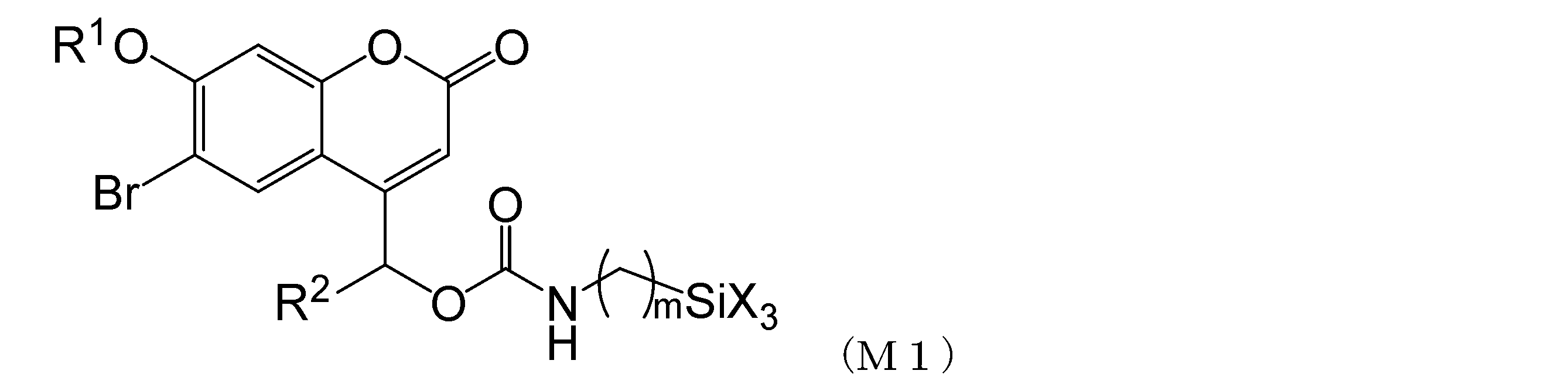
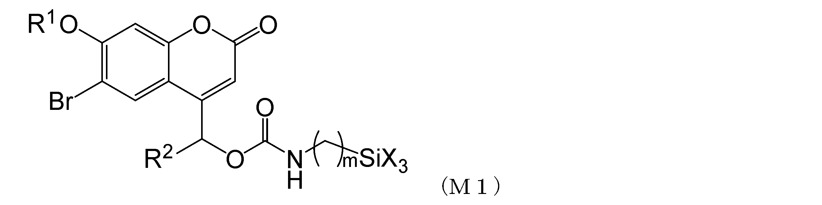
- the first aspect of the present invention is a photosensitive surface treatment agent containing a compound represented by the following formula (M1).
- R 1 is a hydrogen atom, a tert-butoxycarbonyl group, or an ester protecting group
- R 2 is a hydrogen atom or an alkyl group having 1 to 6 carbon atoms
- m is an integer of 1 or more.
- X is a halogen atom or an alkoxy group.
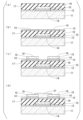
- FIG. 3 is a schematic diagram for explaining the pattern forming method of the present embodiment.
- FIG. 2 is a schematic diagram for explaining a method for manufacturing a transistor according to the present embodiment.
- This is the molecular structure of a resin film on a PET substrate.
- This is an overall image of the PET substrate processed in step 5 of manufacturing plated wiring.
- the photosensitive surface treatment agent of the present invention contains a compound represented by the following formula (M1).
- R 1 is a hydrogen atom, a tert-butoxycarbonyl group, or an ester protecting group
- R 2 is a hydrogen atom or an alkyl group having 1 to 6 carbon atoms
- m is an integer of 1 or more.
- X is a halogen atom or an alkoxy group.
- R 1 is a hydrogen atom, a tert-butoxycarbonyl group, or an ester protecting group.
- ester protecting group examples include an acetyl (Ac) group, a pivaloyl (Pv) group, a propoxycarbonyl group, a tert-butoxycarbonyl group, and a benzoyl group.
- acetal protecting groups such as methoxymethyl (MOM), methoxyethoxymethyl (MEM), and 2-tetrahydropyranyl (THP), methyl, tert.
- R 1 is preferably a tert-butoxycarbonyl group from the viewpoint of stability, high reactivity in protection/deprotection, and ease of synthesis.
- R 2 is a hydrogen atom or an alkyl group having 1 to 6 carbon atoms.
- alkyl group having 1 to 6 carbon atoms include methyl group, ethyl group, propyl group, isopropyl group, n-butyl group, tert-butyl group, hexyl group, and cyclohexyl group.
- m is an integer of 1 or more
- X is a halogen atom or an alkoxy group.
- Examples of the halogen atom represented by X include a fluorine atom, a chlorine atom, a bromine atom, and an iodine atom.
- X is an alkoxy group.
- alkoxy group of X include -O-(CH 3 ) and -O-(CH 2 )n(CH 3 ).
- n is a natural number from 1 to 3.
- the nitrobenzyl groups are eliminated and amines are generated on the substrate surface.
- a metal material, an organic material, or an inorganic material can be brought into close contact with the portion where the amine is generated.
- the photosensitive surface treatment agent of the present embodiment by placing a metal material in the amine-generating portion formed on the substrate surface, line width It is possible to form a metal pattern with a diameter of 5 ⁇ m or less.
- photosensitivity is suppressed in the state of the resin film, after the photosensitive surface treatment agent is applied to the substrate, it can be stored stably without proceeding with photodecomposition. According to the present invention, it is possible to apply a photosensitive surface treatment agent to a substrate, store it, and use it by deprotecting it immediately before pattern formation.
- the deprotection method is specifically acidic conditions using hydrochloric acid, trifluoroacetic acid, etc. Deprotection using hydrolysis below.
- the deprotection method is specifically, under acidic conditions or basic conditions. Deprotection using hydrolysis or hydride reduction.
- the compound represented by formula (M1) can be produced by the following method. First, 6-bromo-4-hydroxymethyl-7-hydroxycoumarin is synthesized by the method described in Examples.
- R 1 is a hydrogen atom by reacting an aminosilane compound with 6-bromo-4-hydroxymethyl-7-hydroxycoumarin.
- a compound represented by formula (M1) can be synthesized.
- Compounds containing a tert-butoxycarbonyl group include, for example, 1-tert-butoxy-2-tert-butoxycarbonyl-1,2-dihydroisoquinoline, di-tert-butyldicarbonate, 1-tert-butoxycarbonyl-1,2, These are 4-triazole, N-(tart-butoxycarbonyloxy)phthalimide, N-tart-butoxycarbonylimidazole, and tert-butylphenyl carbonate.
- the compound represented by formula (M1) is a compound in which R 1 is an ester-based protecting group, first, a compound containing 6-bromo-4-hydroxymethyl-7-hydroxycoumarin and an ester-based protecting group precursor to synthesize an intermediate.
- Examples of compounds containing an ester protecting group include acetyl chloride, acetic anhydride, pivaloyl chloride, pivalic anhydride, benzoyl chloride, and benzoic anhydride.
- the photosensitive surface treatment agent consists of a compound represented by the above formula (M1).
- the photosensitive surface treatment agent may contain a solvent. It can be used as a suitable surface treatment agent by dissolving it in common organic solvents such as alcohol solvents, ester solvents, hydrocarbon aromatic solvents, amine solvents, ketone solvents, glycol ether solvents, and ether solvents. I can do it.
- alcoholic solvents examples include isopropyl alcohol (IPA) and n-butyl alcohol (n-butanol).
- ester solvent examples include ethyl acetate (EAC), butyl acetate (NBAC), n-propyl acetate (NPAC), and 3-methoxy-3-methylbutyl acetate.
- hydrocarbon aromatic solvent examples include toluene, xylene, benzene, ethylbenzene, and trimethylbenzene.
- amine solvent examples include N-methyl-2-pyrrolidone (NMP), dimethylformamide (DMF), and N,N-dimethylacetamide (DMAC).
- NMP N-methyl-2-pyrrolidone
- DMF dimethylformamide
- DMAC N,N-dimethylacetamide
- ketone solvents include methyl ethyl ketone (MEK), methyl isobutyl ketone (MIBK), diisobutyl ketone (DIBK), methyl isopropyl ketone (MIPK), cyclohexanone, cyclopentanone (CPN), cycloheptanone, and acetone. It will be done.
- glycol ether solvents examples include methycellosolve, butycellosolve, ethylene glycol mono t-butyl ether (ETB), propylene glycol monomethyl ether (PGME), proether solvent pyrene glycol monomethyl ether acetate (PGMEA), and 3-methoxy- Examples include 3-methyl-1-butanol (MMB).
- solvents examples include halogenated solvents containing chlorine and fluorine, such as chloroform, chlorobenzene, and fluoroalkyl ether. These may be used alone or in combination of two or more.
- the organic solvent can be appropriately selected depending on conditions such as pollution, solubility, volatility, attack on the substrate or underlayer, film forming apparatus and film forming method.
- alcohol-based, ether-based, or hydrocarbon-based solvents are preferable as the solvent, and in particular, hydrocarbon-based solvents. , among which toluene is preferred.
- any acidic or basic compound may be included during film formation. It can be selected as appropriate depending on the film forming conditions, and acidic compounds such as hydrochloric acid, acetic acid, and nitric acid are particularly preferred, and acetic acid, which allows film formation while maintaining Boc, is particularly preferred.
- the pattern forming method of the present embodiment includes a step of applying the photosensitive surface treatment agent of the present embodiment onto a substrate to form a resin film, a step of deprotecting the resin film, and forming a photosensitive resin film.
- the method includes a step of irradiating a photosensitive resin film with a predetermined pattern of light to form an amine generation region in the exposed region, and a step of arranging an electroless plating catalyst in the amine generation region and performing electroless plating. .
- the photosensitive surface treatment agent of the present embodiment is applied onto a substrate 11 to obtain a resin film 10a.
- coating methods include spin coating, dip coating, die coating, spray coating, roll coating, microgravure, lip coating, inkjet coating, applicator coating, and brush coating.
- the coating may be applied by a printing method such as flexographic printing or screen printing.
- a process of drying the solvent by, for example, heat or reduced pressure may be added.
- the resin film is deprotected to form a photosensitive resin layer 10.
- the deprotection treatment is a hydrolysis treatment under acidic conditions using hydrochloric acid, sulfuric acid, hydrofluoric acid, hexafluoroantimonate, trifluoroacetic acid, or the like.
- the deprotection treatment may be carried out in a liquid phase, or may be carried out in a solid phase by contacting with a gel, film, or the like. Gels, films, etc. may take the form of sheets or rolls.
- a photosensitive surface treatment agent layer 10 is formed on the substrate 11 as shown in FIG. 1(b). Deprotection treatment may be performed immediately after the resin film is formed, or deprotection may be performed immediately before exposure in order to improve the storage stability of the resin film.
- a photomask 13 having a predetermined pattern of exposure areas is prepared.
- the exposure method is not limited to using a photomask, and may include projection exposure using an optical system such as a lens or mirror, maskless exposure using a spatial light modulator, a laser beam, or the like.
- the photomask 13 may be provided so as to be in contact with the photosensitive surface treatment agent layer 10, or may be provided so as not to be in contact with the photosensitive surface treatment agent layer 10.
- the surface of the photosensitive resin layer may be exposed while being immersed in any liquid, or may be exposed after immersion.
- the type of liquid is not particularly limited, but water, alcohol solvents, and ketone solvents can be selected. These may be used alone or in combination of two or more.
- a basic compound may be added to make any basic solution.
- Types of basic compounds include alkali metal carbonates such as sodium hydrogen carbonate and potassium carbonate, alkali metal hydrides such as sodium hydride and sodium tetraborohydride, cesium hydroxide, lithium hydroxide, sodium hydroxide, and hydroxide.
- Alkali metal hydroxides such as potassium, quaternary ammonium salts such as tetramethylammonium hydroxide (TMAH), tetraethylammonium hydroxide (TEAH), tetrapropylammonium hydroxide (TPAH), tetrabutylammonium hydroxide (TBAH), Metal alkoxides such as sodium methoxide and potassium t-butoxide, metal amides such as lithium diisopropylamide (LDA) and potassium hexamethyldisilazide (KHMDS), metal alkyls such as alkyl lithium and alkyl aluminum, pyridine, tetraethylamine, DBU , DBN, imidazole, nitrogen-containing aliphatic compounds, nitrogen-containing heterocyclic compounds, and the like. These may be used alone or in combination of two or more.
- TMAH tetramethylammonium hydroxide
- TEAH tetraethylam
- the liquid preferably has a liquid composition that does not cause peeling, decomposition, or dissolution of the substrate, base, or photosensitive surface treatment agent layer, has good cleaning removability, and has a higher pKa.
- a liquid containing quaternary ammonium is preferred. Particularly preferred is an aqueous solution of tetrabutylammonium hydroxide (TBAH).
- the purpose of increasing pKa is to activate the hydroxy group contained in hydroxycoumarin, increase the molar extinction coefficient, and improve the photoreaction rate. By providing suitable basic conditions, it is possible to improve photoreactivity without damaging the photosensitive surface treatment agent layer.
- the photosensitive surface treatment agent layer 10 is irradiated with UV light through the photomask 13. As a result, the photosensitive surface treatment agent layer 10 is exposed in the exposed area of the photomask 13.
- amine-generating areas 14 are formed in the exposed areas, and amine-ungenerated areas 12 are formed in the unexposed areas.
- UV light is i-line with a wavelength of 365 nm. Further, the exposure amount and exposure time do not necessarily need to be such that complete deprotection occurs, but may be such that some amine is generated.
- an electroless plating catalyst is applied to the surface to form a catalyst layer 15.
- the electroless plating catalyst is a catalyst that reduces metal ions contained in a plating solution for electroless plating, and includes silver and palladium.
- Amino groups are exposed on the surface of the amine generating part 14.
- the amino group can capture and reduce the above-mentioned electroless plating catalyst. Therefore, the electroless plating catalyst is captured only on the amine generating section 14, and the catalyst layer 15 is formed. Further, as the catalyst for electroless plating, a catalyst capable of supporting an amino group can be used.
- electroless plating is performed to form a plating layer 16.
- materials for the plating layer 16 include nickel-phosphorus (NiP) and copper (Cu).
- the substrate 11 is immersed in an electroless plating bath to reduce metal ions to the catalyst surface and deposit a plating layer 16.
- the catalyst layer 15 supporting a sufficient amount of catalyst is formed on the surface of the amine generating part 14, the plating layer 16 can be selectively deposited only on the amine generating part 14.
- an insulator layer 17 is formed by a known method so as to cover the plating layer 16 of the electroless plating pattern formed by the above-described pattern forming method and the amine-free areas 12.
- the insulator layer 17 is formed by applying a coating liquid in which one or more resins such as ultraviolet curable acrylic resin, epoxy resin, ene-thiol resin, silicone resin, etc. are dissolved in an organic solvent. It may also be formed by The insulator layer 17 can be formed into a desired pattern by irradiating the coating film with ultraviolet rays through a mask provided with openings corresponding to the regions where the insulator layer 17 is to be formed. Note that, before forming the insulator layer 17, the amine-free portion 12 may be removed if necessary.
- a photosensitive surface treatment agent layer 10 is formed on the insulator layer 17 in the same manner as the electroless plating pattern forming method described above, and the photosensitive surface treatment agent layer 10 is formed on the portion where the source electrode and the drain electrode are to be formed.
- An amine generating section 14 is formed.
- an electroless plating catalyst is supported on the amine generating portion 14, a catalyst layer 15 is formed, and then electroless plating is performed.
- a plating layer 18 (source electrode) and a plating layer 19 (drain electrode) are formed.
- the materials for the plating layers 18 and 19 include nickel-phosphorus (NiP) and copper (Cu), but they may also be formed of a material different from that of the plating layer 16 (gate electrode). ), or gold (Au) may be deposited by performing electroless gold plating on the surface of copper (Cu) with a different metal, such as electroless gold plating.
- a semiconductor layer 21 is formed between the plating layer 18 (source electrode) and the plating layer 19 (drain electrode).
- the semiconductor layer 21 is formed by preparing a solution in which an organic semiconductor material soluble in an organic solvent, such as TIPS pentacene (6,13-Bis (triisopropylsilylthynyl) pentacene), is dissolved in the organic solvent. It may also be formed by coating and drying between the electrode) and the plating layer 19 (drain electrode).
- an organic semiconductor material soluble in an organic solvent such as TIPS pentacene (6,13-Bis (triisopropylsilylthynyl) pentacene
- the semiconductor layer 21 is formed by adding one or more types of insulating polymer such as PS (polystyrene) or PMMA (polymethyl methacrylate) to the above solution, applying the solution containing the insulating polymer, and drying. It's okay.
- insulating polymer such as PS (polystyrene) or PMMA (polymethyl methacrylate)
- the insulating polymer is formed in a concentrated manner below the semiconductor layer 21 (on the insulator layer 17 side).
- a polar group such as an amino group
- transistor characteristics tend to deteriorate; however, by providing the organic semiconductor through the above-mentioned insulating polymer, Deterioration of transistor characteristics can be suppressed. It is possible to manufacture a transistor in the manner described above.
- the resin film protected by BOC is extremely stable against light, and does not require light-shielding storage or work in a yellow room, from the surface treatment agent state to the film formation process, and the resin film after formation. This significantly improves workability and storage stability compared to the handling of general photosensitive materials. Since photosensitivity is obtained after deprotection treatment, the number of processes that require light control can be significantly reduced, reducing the burden on workers.
- top contact/bottom gate type, top contact/top gate type, and bottom contact/top gate type transistors may be manufactured in the same manner.
- This embodiment is a laminate containing the photosensitive surface treatment agent of this embodiment.
- the laminate of this embodiment is a laminate in which a substrate and a metal pattern are laminated, and includes a photosensitive surface treatment agent in an unexposed area where a pattern is not formed.
- This embodiment is a transistor containing the photosensitive surface treatment agent of this embodiment.
- the laminate of this embodiment is a transistor having a laminate in which a substrate and a metal pattern are laminated, and includes a photosensitive surface treatment agent in an unexposed area where a pattern is not formed.
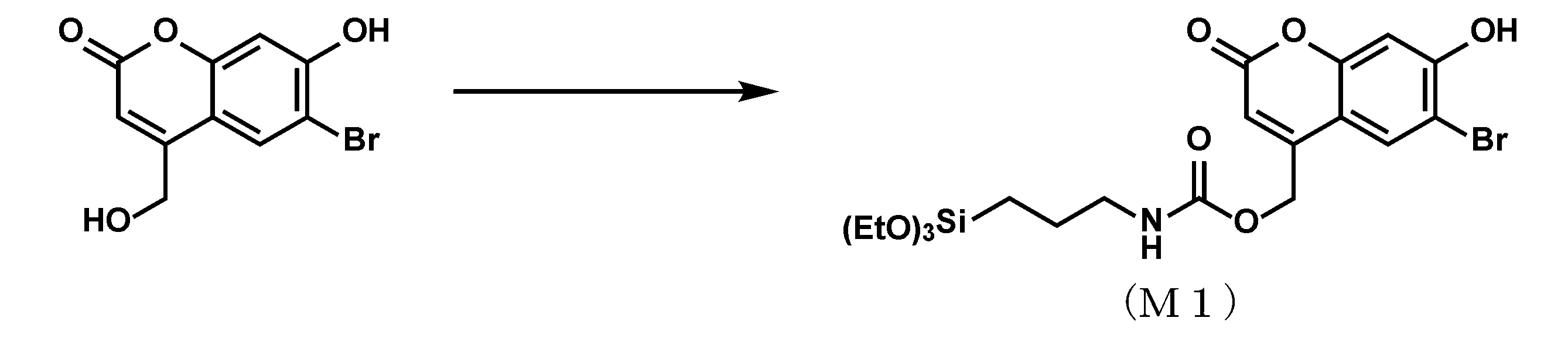
- Example 1 A compound represented by (M1)-11 was obtained using the following synthesis scheme. First, 6-bromo-4-chloromethyl-7-hydroxycoumarin was synthesized by the reaction shown below.
- Extract by adding ethyl acetate (10 mL x 3) and 1N HCl (10 mL), wash sequentially with saturated NaHCO 3 aqueous solution (10 mL x 1) and saturated brine (10 mL x 1), dry the organic layer with anhydrous MgSO 4 and filter. , concentrated and dried under vacuum to obtain 990 mg of a brown solid. Purify by column chromatography (silica gel 100 cc, diameter 3.0 cm, height 15 cm) (suspend in developing solvent and charge, developing solvent chloroform:ethyl acetate 5:1 (Rf 0.29, 300 mL)), concentrate, and vacuum It was dried to obtain 835 mg (2.25 mmol, 76%) of the target product as a white solid.
- Toluene was added to the compound represented by formula (M1)-11 synthesized in Example 1 to adjust the concentration to 0.1% by mass, and then acetic acid was added at a rate such that the acetic acid concentration was 1.0% by mass to form a photosensitive surface. Processing agent 1 was obtained.
- Photosensitive surface treatment agent 1 was placed in a 1.4 L glass container, heated to 60°C using a hot water bath, and then the substrate was immersed for 90 minutes to form a SiO 2 film on the surface of the PET substrate (Oike).
- a compound represented by (M1)-11 was chemically bonded onto VX-50TUH (manufactured by Advanced Film Co., Ltd.) to form a resin film. Thereafter, the physically attached compound was removed by immersing the substrate in methanol and irradiating it with 28 kHz ultrasonic waves for 3 minutes, thereby obtaining a resin film with strong adhesion.
- the resin film was deprotected by immersing it in a 50:50 mixed solution of 35% hydrochloric acid aqueous solution and methanol for 30 minutes at room temperature to obtain a photosensitive surface treatment agent layer.
- the tert-butoxycarbonyl group of the compound represented by formula (M1)-11 was removed and a hydroxyl group was generated, as shown below, to obtain a photosensitive resin layer.
- the substrate on which the photosensitive surface treatment agent layer has been formed is exposed to 250 mJ/ cm2 of light with a wavelength of 365 nm through a photomask to expose the photosensitive surface treatment agent layer to light, and the exposed area has amino groups. A non-generated portion of amino groups was formed in the unexposed portion.
- a plated wiring was produced in the same manner as described in [Manufacture of plated wiring 1] above, except that the exposure amount was changed to 500 mJ/cm 2 .
- a plated wiring was produced in the same manner as described in [Manufacture of plated wiring 1] above, except that the exposure amount was changed to 1000 mJ/cm 2 .
- a plated wiring was produced in the same manner as described in [Manufacture of plated wiring 1] above, except that the exposure amount was changed to 2000 mJ/cm 2 .
- a plated wiring was produced in the same manner as described in [Manufacture of plated wiring 1] above, except that the resin film was not deprotected and the dry substrate was exposed to light with a wavelength of 365 nm at 2000 mJ/cm 2 .
- FIGS. 3A and 3B show optical microscope images (manufactured by Keyence Corporation, VHX-7000) of the PET substrate that was subjected to the plating wiring treatment in the example.
- FIGS. 4A and 4B show the results of exposure and plating wiring processing performed on the resin film in the example.
- FIG. 4A shows the molecular structure of the resin film on the PET substrate.
- FIG. 4B is an overall image of the PET substrate processed in step 5 of manufacturing plated wiring. From FIG. 4A and FIG. 4B, even when irradiated with 2000 mJ/ cm2 of light with a wavelength of 365 nm, unintended generation of amines can be suppressed without deprotection, and in the state of the resin film, unintentional amine generation can be suppressed. None generated. In other words, it was confirmed that it has excellent photostability and does not need to be stored in the dark.
Landscapes
- Physics & Mathematics (AREA)
- General Physics & Mathematics (AREA)
- Chemical & Material Sciences (AREA)
- Organic Chemistry (AREA)
- Spectroscopy & Molecular Physics (AREA)
- Engineering & Computer Science (AREA)
- Materials Engineering (AREA)
- Chemical Kinetics & Catalysis (AREA)
- Mechanical Engineering (AREA)
- Metallurgy (AREA)
- General Chemical & Material Sciences (AREA)
- Materials For Photolithography (AREA)
- Electrodes Of Semiconductors (AREA)
- Thin Film Transistor (AREA)
- Photosensitive Polymer And Photoresist Processing (AREA)
Abstract
Description
本願は、2022年8月22日に、日本に出願された特願2022-131902号に基づき優先権を主張し、その内容をここに援用する。
本発明の感光性表面処理剤は、下記式(M1)で表される化合物を含む。
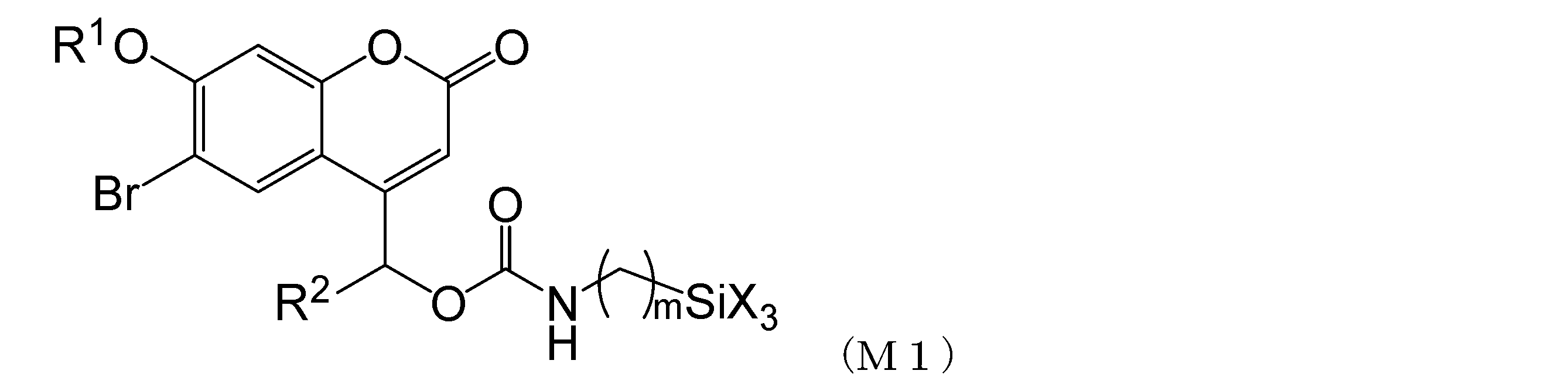




式(M1)で表される化合物は、以下の方法により製造できる。
まず、実施例に記載の方法により、6-ブロモ-4-ヒドロキシメチル-7-ヒドロキシクマリンを合成する。
本実施形態のパターン形成方法は、前記本実施形態の感光性表面処理剤を基板上に塗布し、樹脂膜を成膜する工程と、樹脂膜を脱保護し、感光性樹脂膜する工程と、感光性樹脂膜に所定のパターンの光を照射して、露光領域にアミン発生領域を形成する工程と、アミン発生領域に無電解めっき用触媒を配置し、無電解めっきを行う工程と、を備える。
以下、各工程について図面を参照して説明する。
塗布方法としては、例えば、スピンコート法、ディップコート法、ダイコート法、スプレーコート法、ロールコート法、マイクログラビア法、リップコート法、インクジェット法、アプリケーター塗布、刷毛塗り等の塗布方法使用できる。また、フレキソ印刷、スクリーン印刷等の印刷法により塗布してもよい。
これにより、図1(b)に示すように基板11の上に感光性表面処理剤層10が形成される。
樹脂膜の成膜直後に脱保護処理してもよく、樹脂膜の保管安定性を高めるために露光直前に脱保護してもよい。
さらに、上記<パターン形成方法>で得られためっき層16をゲート電極とするトランジスタの製造方法について図2を用いて説明する。
本実施形態は、前記本実施形態の感光性表面処理剤を含む積層体である。
本実施形態の積層体は、基板と金属パターンとが積層された積層体であって、パターンが形成されていない未露光部に感光性表面処理剤を含む。
本実施形態は、前記本実施形態の感光性表面処理剤を含むトランジスタである。
本実施形態の積層体は、基板と金属パターンとが積層された積層体を有するトランジスタであって、パターンが形成されていない未露光部に感光性表面処理剤を含む。
下記の合成スキームで(M1)-11で表される化合物を得た。
まず、下記に示す反応により、6-ブロモ-4-クロロメチル-7-ヒドロキシクマリンを合成した。



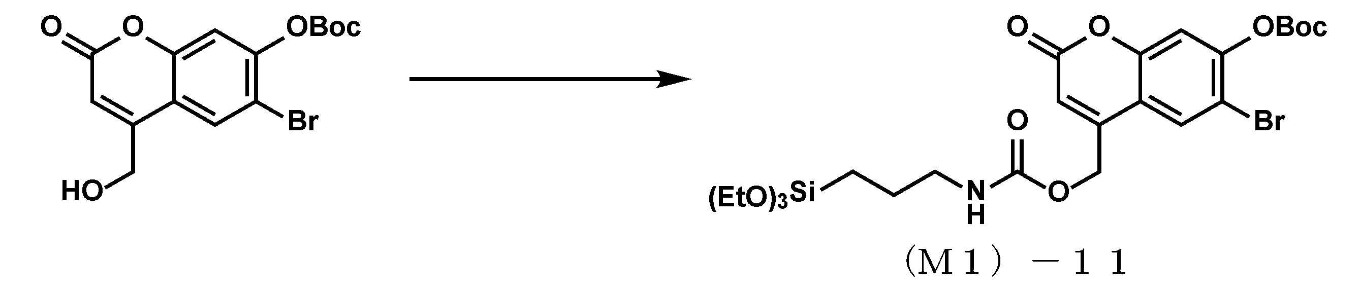
以下に示す反応により、6-ブロモ-7-ヒドロキシクマリン-4-イルメチル 3-(トリエトキシシリル)プロピルカルバメート(M1)を合成した。
Rf=0.25(クロロホルム:酢酸エチル=20:1)
[めっき配線の製造1]
式(M1)-11で表される化合物を含む表面処理剤を用いて基板上に成膜し、めっき配線を製造した。
樹脂膜を脱保護処理することで、下記に示すように式(M1)-11で表される化合物のtert-ブトキシカルボニル基が脱離し、ヒドロキシ基が発生し、感光性樹脂層を得た。

樹脂膜を浸漬することで、式(M1)-11で表される化合物のヒドロキシ基が塩基により活性化され、モル吸光係数の増加とともに光反応速度が向上し、高感度な感光性表面処理剤層を得た。
露光量を500mJ/cm2に変更した以外は、上記[めっき配線の製造1]に記載の方法と同様にめっき配線を作製した。
露光量を1000mJ/cm2に変更した以外は、上記[めっき配線の製造1]に記載の方法と同様にめっき配線を作製した。
露光量を2000mJ/cm2に変更した以外は、上記[めっき配線の製造1]に記載の方法と同様にめっき配線を作製した。
樹脂膜を脱保護処理行わず、乾燥基板のまま波長365nm光を2000mJ/cm2露光に変更した以外は、上記[めっき配線の製造1]に記載の方法と同様にめっき配線を作製した。
図3A、図3Bに実施例でめっき配線処理を行った、PET基板の光学顕微鏡(株式会社キーエンス製、VHX-7000)像をそれぞれ示す。
図3Aは、PET基板に上記めっき配線の製造1~4で加工したL/S=100/100、5/5の光学顕微鏡像である。
図3Bは、PET基板に上記めっき配線の製造3で加工したL/S=1/1~9/9umの光学顕微鏡像である。
図4Bは、上記めっき配線の製造5で加工したPET基板の全体像である。
図4A及び図4Bから、波長365nm光を2000mJ/cm2照射してもなお、脱保護されることなく意図しないアミンの発生を抑制できており、樹脂膜の状態であれば意図せずアミンが生成されることがない。すなわち光安定性に優れ遮光保管する必要がないことが確認できた。
Claims (13)
- 下記式(M1)で表される化合物を含む、感光性表面処理剤。
- 請求項1に記載の感光性表面処理剤を用いて化学修飾された表面を有するパターン形成用基板。
- 請求項1に記載の感光性表面処理剤を含む積層体。
- 請求項1に記載の感光性表面処理剤を含むトランジスタ。
- 請求項1に記載の感光性表面処理剤を基板上に塗布し、樹脂膜を成膜する工程と、
前記樹脂膜を脱保護し、感光性樹脂膜にする工程と、
前記感光性樹脂膜に所定のパターンの光を照射する工程と、
前記所定のパターン光の照射領域の少なくとも一部の領域に対して無電解めっきを行う工程と、を備える、パターン形成方法。 - 請求項1に記載の感光性表面処理剤を基板上に塗布し、樹脂膜を成膜する工程と、
前記樹脂膜を脱保護し、感光性樹脂膜にする工程と、
前記感光性樹脂膜に所定のパターンの光を照射する工程と、
前記所定のパターン光の照射領域の少なくとも一部の領域に無電解めっき用触媒を配置し、無電解めっきを行う工程と、を備える、パターン形成方法。 - 請求項1に記載の感光性表面処理剤を基板上に塗布し、樹脂膜を成膜する工程と、
前記樹脂膜を脱保護し、感光性樹脂膜にする工程と、
前記感光性樹脂膜に所定のパターンの光を照射して、露光領域にアミン発生領域を形成する工程と、
前記アミン発生領域に無電解めっき用触媒を配置し、無電解めっきを行う工程と、を備える、パターン形成方法。 - 請求項1に記載の感光性表面処理剤を基板上に塗布し、樹脂膜を成膜する工程と、
前記樹脂膜を脱保護し、感光性樹脂膜にする工程と、
前記感光性樹脂膜を塩基性溶液に浸漬する工程と、
前記塩基性溶液に浸漬した後、前記感光性樹脂膜に所定のパターンの光を照射して、露光領域にアミン発生領域を形成する工程と、
前記アミン発生領域に無電解めっき用触媒を配置し、無電解めっきを行う工程と、を備える、パターン形成方法。 - 請求項1に記載の感光性表面処理剤を基板上に塗布し、樹脂膜を成膜する工程と、
前記樹脂膜を脱保護し、感光性樹脂膜にする工程と、
前記感光性樹脂膜を塩基性溶液に浸漬する工程と、
前記塩基性溶液に浸漬しながら、前記感光性樹脂膜に所定のパターンの光を照射して、露光領域にアミン発生領域を形成する工程と、
前記アミン発生領域に無電解めっき用触媒を配置し、無電解めっきを行う工程と、を備える、パターン形成方法。 - 前記塩基性溶液は、水酸化テトラブチラムモニウム(TBAH)水溶液である、請求項8または9に記載のパターン形成方法。
- 請求項5又は6に記載のパターン形成方法により、ソース電極、ドレイン電極、またはゲート電極のうちいずれか1以上の電極を形成する工程を含む、トランジスタの製造方法。
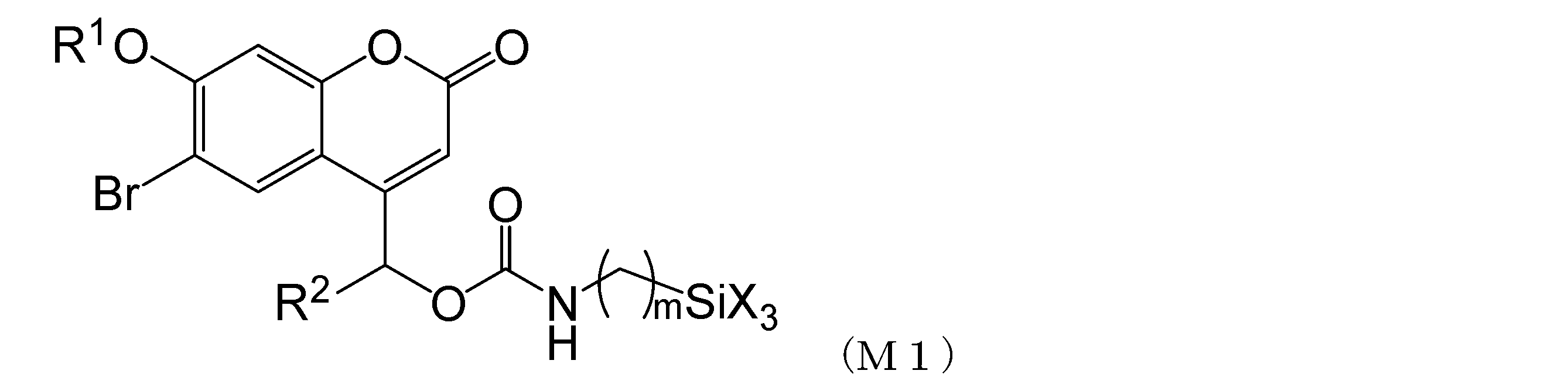
- 下記式(M1)で表される化合物を含む、トランジスタ。
- 前記化合物は、少なくとも一部のニトロベンジル基が脱離してアミノ基が発生した部分を有する、請求項12に記載のトランジスタ。
Priority Applications (3)
| Application Number | Priority Date | Filing Date | Title |
|---|---|---|---|
| KR1020257004982A KR102897547B1 (ko) | 2022-08-22 | 2023-08-22 | 감광성 표면 처리제, 패턴 형성용 기판, 적층체, 트랜지스터, 패턴 형성 방법 및 트랜지스터의 제조 방법 |
| CN202380056457.1A CN119631019A (zh) | 2022-08-22 | 2023-08-22 | 感光性表面处理剂、图案形成用基板、层积体、晶体管、图案形成方法和晶体管的制造方法 |
| US19/057,306 US20250189894A1 (en) | 2022-08-22 | 2025-02-19 | Photosensitive surface treating agent, pattern formation substrate, laminate, transistor, pattern forming method and method of producing transistor |
Applications Claiming Priority (2)
| Application Number | Priority Date | Filing Date | Title |
|---|---|---|---|
| JP2022-131902 | 2022-08-22 | ||
| JP2022131902A JP7868450B2 (ja) | 2022-08-22 | 2022-08-22 | 感光性表面処理剤、パターン形成用基板、積層体、トランジスタ、パターン形成方法及びトランジスタの製造方法 |
Related Child Applications (1)
| Application Number | Title | Priority Date | Filing Date |
|---|---|---|---|
| US19/057,306 Continuation US20250189894A1 (en) | 2022-08-22 | 2025-02-19 | Photosensitive surface treating agent, pattern formation substrate, laminate, transistor, pattern forming method and method of producing transistor |
Publications (1)
| Publication Number | Publication Date |
|---|---|
| WO2024043221A1 true WO2024043221A1 (ja) | 2024-02-29 |
Family
ID=90013344
Family Applications (1)
| Application Number | Title | Priority Date | Filing Date |
|---|---|---|---|
| PCT/JP2023/030083 Ceased WO2024043221A1 (ja) | 2022-08-22 | 2023-08-22 | 感光性表面処理剤、パターン形成用基板、積層体、トランジスタ、パターン形成方法及びトランジスタの製造方法 |
Country Status (5)
| Country | Link |
|---|---|
| US (1) | US20250189894A1 (ja) |
| JP (1) | JP7868450B2 (ja) |
| KR (1) | KR102897547B1 (ja) |
| CN (1) | CN119631019A (ja) |
| WO (1) | WO2024043221A1 (ja) |
Citations (5)
| Publication number | Priority date | Publication date | Assignee | Title |
|---|---|---|---|---|
| JP2003321479A (ja) * | 2002-05-02 | 2003-11-11 | Japan Science & Technology Corp | 光分解性シランカップリング剤 |
| JP2011225645A (ja) * | 2010-04-15 | 2011-11-10 | Tokyo Univ Of Science | エポキシ樹脂硬化用微粒子及びエポキシ樹脂硬化用微粒子の製造方法 |
| WO2015129799A1 (ja) * | 2014-02-28 | 2015-09-03 | 株式会社ニコン | 配線パターンの製造方法およびトランジスタの製造方法 |
| WO2016163525A1 (ja) * | 2015-04-10 | 2016-10-13 | 株式会社ニコン | 高分子化合物、表面処理剤、表面処理剤を用いた積層体、トランジスタ、積層体の製造方法 |
| WO2021010370A1 (ja) * | 2019-07-12 | 2021-01-21 | 株式会社ニコン | 基板処理方法、パターン形成方法、及び基板処理システム |
Family Cites Families (2)
| Publication number | Priority date | Publication date | Assignee | Title |
|---|---|---|---|---|
| JP2006002201A (ja) | 2004-06-16 | 2006-01-05 | Hitachi Maxell Ltd | メッキ膜被覆構造部材、メッキ膜が被覆された構造部材の製造方法および光学モジュール |
| JP7121505B2 (ja) * | 2017-10-11 | 2022-08-18 | 株式会社ニコン | 化合物、パターン形成用基板、光分解性カップリング剤、パターン形成方法及びトランジスタの製造方法 |
-
2022
- 2022-08-22 JP JP2022131902A patent/JP7868450B2/ja active Active
-
2023
- 2023-08-22 WO PCT/JP2023/030083 patent/WO2024043221A1/ja not_active Ceased
- 2023-08-22 KR KR1020257004982A patent/KR102897547B1/ko active Active
- 2023-08-22 CN CN202380056457.1A patent/CN119631019A/zh active Pending
-
2025
- 2025-02-19 US US19/057,306 patent/US20250189894A1/en active Pending
Patent Citations (5)
| Publication number | Priority date | Publication date | Assignee | Title |
|---|---|---|---|---|
| JP2003321479A (ja) * | 2002-05-02 | 2003-11-11 | Japan Science & Technology Corp | 光分解性シランカップリング剤 |
| JP2011225645A (ja) * | 2010-04-15 | 2011-11-10 | Tokyo Univ Of Science | エポキシ樹脂硬化用微粒子及びエポキシ樹脂硬化用微粒子の製造方法 |
| WO2015129799A1 (ja) * | 2014-02-28 | 2015-09-03 | 株式会社ニコン | 配線パターンの製造方法およびトランジスタの製造方法 |
| WO2016163525A1 (ja) * | 2015-04-10 | 2016-10-13 | 株式会社ニコン | 高分子化合物、表面処理剤、表面処理剤を用いた積層体、トランジスタ、積層体の製造方法 |
| WO2021010370A1 (ja) * | 2019-07-12 | 2021-01-21 | 株式会社ニコン | 基板処理方法、パターン形成方法、及び基板処理システム |
Also Published As
| Publication number | Publication date |
|---|---|
| KR20250039424A (ko) | 2025-03-20 |
| JP7868450B2 (ja) | 2026-06-02 |
| CN119631019A (zh) | 2025-03-14 |
| KR102897547B1 (ko) | 2025-12-08 |
| JP2024029570A (ja) | 2024-03-06 |
| US20250189894A1 (en) | 2025-06-12 |
Similar Documents
| Publication | Publication Date | Title |
|---|---|---|
| JP7121505B2 (ja) | 化合物、パターン形成用基板、光分解性カップリング剤、パターン形成方法及びトランジスタの製造方法 | |
| US20250180990A1 (en) | Photosensitive surface treating agent, laminate, pattern formation substrate, transistor, pattern forming method and method of producing transistor | |
| TW200811224A (en) | Silsesquioxane resin systems with base additives bearing electron-attracting functionalities | |
| US20250004366A1 (en) | Resist composition, resist pattern formation method, compound, acid-generating agent, acid diffusion control agent, and high-molecular-weight compound | |
| TW201229660A (en) | Radio-sensitive resin composition and pattern forming method | |
| KR102897547B1 (ko) | 감광성 표면 처리제, 패턴 형성용 기판, 적층체, 트랜지스터, 패턴 형성 방법 및 트랜지스터의 제조 방법 | |
| JP5110507B2 (ja) | 反応現像画像形成法 | |
| CN105980347B (zh) | 新型脂环式酯化合物的制造方法、新型脂环式酯化合物、将其聚合的(甲基)丙烯酸系共聚物、和包含其的感光性树脂组合物 | |
| JP6832727B2 (ja) | 化合物、パターン形成用基板、光分解性カップリング剤、パターン形成方法及びトランジスタの製造方法 | |
| JP2025113997A (ja) | レジスト組成物及びそれを利用したパターン形成方法 | |
| JP7732272B2 (ja) | 感光性表面処理剤、積層体、トランジスタ、パターン形成方法及びトランジスタの製造方法 | |
| JP5827058B2 (ja) | シルセスキオキサン化合物の製造方法 | |
| JP2025054216A (ja) | 有機金属化合物、それを含むレジスト組成物、及びそれを利用したパターン形成方法 | |
| US7147985B2 (en) | Resist compounds including acid labile groups having hydrophilic groups attached thereto | |
| JP2024036931A (ja) | かご構造を有するシルセスキオキサン及びレジスト組成物 | |
| CN119256273A (zh) | 可显影的抗蚀剂上层膜组合物以及制造抗蚀剂上层膜图案及抗蚀剂图案的方法 | |
| TW201414712A (zh) | 光酸產生劑及其製備方法、以及含有該光酸產生劑的抗蝕劑組成物及化合物 | |
| TWI498340B (zh) | Linear radiation-sensitive resin composition | |
| US20250386722A1 (en) | Compound, polymer compound, photosensitive surface treatment agent, laminate, substrate for pattern formation, transistor, pattern formation method, and transistor manufacturing method | |
| EP4194949A1 (en) | Photoacid generator, photoresist composition including the same, and method of forming a pattern using the photoacid generator | |
| TW201939175A (zh) | 圖案形成方法及顯影液 | |
| JP2010191409A (ja) | 酸転写用組成物、酸転写用膜及びパターン形成方法 | |
| WO2026100410A1 (ja) | ヨウ素含有重合性化合物及びヨウ素含有重合体 | |
| TW202447349A (zh) | 抗蝕劑底層膜形成用組成物、半導體基板的製造方法及抗蝕劑底層膜形成用聚合物 | |
| CN118255802A (zh) | 有机金属化合物、包括其的抗蚀剂组合物和使用其的图案形成方法 |
Legal Events
| Date | Code | Title | Description |
|---|---|---|---|
| 121 | Ep: the epo has been informed by wipo that ep was designated in this application |
Ref document number: 23857330 Country of ref document: EP Kind code of ref document: A1 |
|
| WWE | Wipo information: entry into national phase |
Ref document number: 202380056457.1 Country of ref document: CN |
|
| ENP | Entry into the national phase |
Ref document number: 20257004982 Country of ref document: KR Kind code of ref document: A |
|
| WWE | Wipo information: entry into national phase |
Ref document number: 1020257004982 Country of ref document: KR |
|
| WWP | Wipo information: published in national office |
Ref document number: 202380056457.1 Country of ref document: CN |
|
| WWP | Wipo information: published in national office |
Ref document number: 1020257004982 Country of ref document: KR |
|
| NENP | Non-entry into the national phase |
Ref country code: DE |
|
| 122 | Ep: pct application non-entry in european phase |
Ref document number: 23857330 Country of ref document: EP Kind code of ref document: A1 |