WO2024042863A1 - 撮像装置 - Google Patents
撮像装置 Download PDFInfo
- Publication number
- WO2024042863A1 WO2024042863A1 PCT/JP2023/024429 JP2023024429W WO2024042863A1 WO 2024042863 A1 WO2024042863 A1 WO 2024042863A1 JP 2023024429 W JP2023024429 W JP 2023024429W WO 2024042863 A1 WO2024042863 A1 WO 2024042863A1
- Authority
- WO
- WIPO (PCT)
- Prior art keywords
- signal line
- transistor
- pixel
- signal
- imaging device
- Prior art date
- Legal status (The legal status is an assumption and is not a legal conclusion. Google has not performed a legal analysis and makes no representation as to the accuracy of the status listed.)
- Ceased
Links
Images










Classifications
-
- H—ELECTRICITY
- H04—ELECTRIC COMMUNICATION TECHNIQUE
- H04N—PICTORIAL COMMUNICATION, e.g. TELEVISION
- H04N25/00—Circuitry of solid-state image sensors [SSIS]; Control thereof
- H04N25/70—SSIS architectures; Circuits associated therewith
- H04N25/76—Addressed sensors, e.g. MOS or CMOS sensors
- H04N25/78—Readout circuits for addressed sensors, e.g. output amplifiers or A/D converters
-
- H—ELECTRICITY
- H04—ELECTRIC COMMUNICATION TECHNIQUE
- H04N—PICTORIAL COMMUNICATION, e.g. TELEVISION
- H04N25/00—Circuitry of solid-state image sensors [SSIS]; Control thereof
- H04N25/60—Noise processing, e.g. detecting, correcting, reducing or removing noise
- H04N25/62—Detection or reduction of noise due to excess charges produced by the exposure, e.g. smear, blooming, ghost image, crosstalk or leakage between pixels
- H04N25/627—Detection or reduction of inverted contrast or eclipsing effects
-
- H—ELECTRICITY
- H04—ELECTRIC COMMUNICATION TECHNIQUE
- H04N—PICTORIAL COMMUNICATION, e.g. TELEVISION
- H04N25/00—Circuitry of solid-state image sensors [SSIS]; Control thereof
- H04N25/70—SSIS architectures; Circuits associated therewith
- H04N25/76—Addressed sensors, e.g. MOS or CMOS sensors
- H04N25/77—Pixel circuitry, e.g. memories, A/D converters, pixel amplifiers, shared circuits or shared components
- H04N25/771—Pixel circuitry, e.g. memories, A/D converters, pixel amplifiers, shared circuits or shared components comprising storage means other than floating diffusion
-
- H—ELECTRICITY
- H04—ELECTRIC COMMUNICATION TECHNIQUE
- H04N—PICTORIAL COMMUNICATION, e.g. TELEVISION
- H04N25/00—Circuitry of solid-state image sensors [SSIS]; Control thereof
- H04N25/60—Noise processing, e.g. detecting, correcting, reducing or removing noise
- H04N25/67—Noise processing, e.g. detecting, correcting, reducing or removing noise applied to fixed-pattern noise, e.g. non-uniformity of response
Definitions
- the present technology relates to an imaging device. Specifically, the present technology relates to an imaging device that can prevent black level output due to incidence of high-intensity light.
- a capacitive load readout method is known in which a capacitor is used as the load of a source follower when reading signals from a pixel.
- a capacitive load readout method for example, an imaging device has been proposed in which a reset unit resets the voltage of the output line, and then a constant current source causes a constant current to flow through the output line, and the source of the amplification transistor is connected to the output line. (For example, see Patent Document 1).
- This technology was created in view of this situation, and its purpose is to make it possible to prevent black level output due to the incidence of high-intensity light.
- the signal line has a potential that changes based on the electric charge accumulated in accordance with the current that flows when reading signals from the pixel.
- a signal line reset transistor that resets the potential of the signal line;
- a signal line reset level generation section that generates a reset level of the potential of the signal line;
- a signal line clip transistor that clips the potential of the signal line;
- the imaging apparatus includes a signal line clipping voltage setting section that sets a signal line clipping voltage used to generate a clipping level of the potential of the signal line. This brings about the effect that the potential of the signal line is clipped regardless of the amount of incident light.
- the potential of the signal line may be a potential of a parasitic capacitance of the signal line. This brings about the effect that capacitive load reading can be performed without adding a capacitive element to the signal line.
- the pixel includes a photodiode, a transfer transistor that transfers the charge accumulated in the photodiode to the floating diffusion, a reset transistor that resets the floating diffusion, and a potential of the floating diffusion.
- the device may include an amplification transistor that outputs a corresponding signal, and a selection transistor connected between the amplification transistor and the signal line. This brings about the effect that a source follower is formed between the pixel and the pixel when a signal is read from the pixel.
- the signal line reset level generation section may include a diode-connected transistor. This brings about the effect that the potential of the signal line is raised in accordance with the forward voltage of the diode-connected transistor when the signal line is reset.
- the device may further include a driver that drives the signal line reset transistor. This brings about the effect that the signal line reset transistor is turned on/off.
- a signal line clip selection transistor may be further provided connected between the signal line and the signal line clip transistor. This brings about the effect of controlling the application of the clip level to the signal line.
- a first chip in which the pixel, the signal line clip transistor, and the signal line clip selection transistor are formed, and the first chip are stacked, and the signal line reset transistor and the signal line reset transistor are stacked.
- the second chip may include a level generation section and a second chip in which the signal line clip voltage setting section is formed.
- the gate length and gate width of the signal line clip transistor are equal to the gate length and gate width of the amplification transistor of the pixel
- the gate length and gate width of the signal line clip selection transistor are equal to the gate length and gate width of the signal line clip selection transistor. It may be equal to the gate length and gate width of the selection transistor of the pixel. This brings about the effect that the characteristics of the signal line clip transistor and the characteristics of the pixel amplification transistor become equal, and the characteristics of the signal line clip selection transistor and the characteristics of the pixel selection transistor become equal.
- the signal line may be simultaneously driven by the signal line clip selection transistor and the amplification transistor of the pixel. This brings about the effect of increasing the driving force of the signal line.
- the device may further include a comparator that compares the potential of the signal line and the ramp signal. This brings about the effect that the signal read from the pixel can be detected based on the potential of the signal line.
- a comparator may be further provided to compare the potentials of the signal lines provided in different columns. This brings about the effect that the edge of the object is detected based on the capacitive load readout.
- a first DC cut capacitor connected to a first input terminal of the comparator, a second DC cut capacitor connected to a second input terminal of the comparator, and a first DC cut capacitor connected to a second input terminal of the comparator, and a first
- the apparatus may further include an auto-zero control section that controls charges accumulated in the first DC cut capacitor and the second DC cut capacitor, respectively, so that the input and the second input are balanced. This brings about the effect that fixed pattern noise is reduced.
- the signal line clip selection transistor may be turned off after the auto-zero period. This brings about the effect that when the signal line is clipped, the non-inverting input and the inverting input of the comparator are adjusted to be balanced.
- the signal line clipping voltage may be lower than the reset level of the pixel. This brings about the effect that the reset level of the pixel can be read.
- the device may further include a constant current transistor that is electrically connectable to the signal line and that flows a constant current based on a source follower formed between the pixel and the pixel. This brings about the effect that constant current reading is possible when capacitive load reading is not performed.
- the constant current transistor is turned on in constant current readout using the constant current transistor, and the constant current transistor is turned off in capacitive load readout using the signal line reset level generation section. It's okay. This brings about the effect that capacitive load readout and constant current readout can be switched.
- the signal line clip voltage setting section may generate a plurality of clip levels. This brings about the effect that the clip level of the signal line is adjusted.
- the signal line clipping voltage setting section may include a resistance ladder circuit and a first selector that switches the divided voltage generated by the resistance ladder circuit. This brings about the effect of switching the clip level of the signal line.
- the signal line reset level generation section may include a second selector that switches the divided voltage generated by the resistance ladder circuit. This brings about the effect that the reset level and clip level of the signal line can be switched separately.
- the pixel array section includes a pixel array section in which the pixels are arranged in a matrix in a row direction and a column direction, the signal line is provided for each column, and the signal line reset transistor and the signal line clip are provided.
- a transistor may be provided in each of the signal lines. This brings about the effect that the potential of the signal line is reset and clipped for each signal line.
- FIG. 1 is a block diagram illustrating a configuration example of a camera to which the imaging device according to the first embodiment is applied.
- 1 is a block diagram showing a configuration example of a solid-state imaging device according to a first embodiment.
- FIG. FIG. 2 is a block diagram showing an example of a circuit configuration of a pixel provided in the solid-state imaging device according to the first embodiment.
- FIG. 2 is a cross-sectional view showing a configuration example of a pixel array section provided in the solid-state imaging device according to the first embodiment.
- FIG. 7 is a cross-sectional view showing a modification of the pixel array section provided in the solid-state imaging device according to the first embodiment.
- FIG. 3 is a diagram illustrating a configuration example of a signal readout circuit for one column according to the first embodiment.
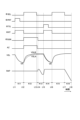
- FIG. 3 is a diagram showing a first example of waveforms of various parts during signal readout of the imaging device according to the first embodiment.
- FIG. 7 is a diagram illustrating a second example of waveforms of various parts during signal readout of the imaging device according to the first embodiment.
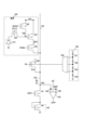
- FIG. 7 is a diagram showing a configuration example of a signal readout circuit for one column according to a second embodiment.
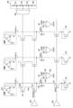
- FIG. 7 is a diagram showing a configuration example of a signal readout circuit for three columns according to a third embodiment.
- FIG. 12 is a diagram showing a configuration example of a signal readout circuit for one column according to a fourth embodiment.
- FIG. 3 is a diagram illustrating a configuration example of a signal readout circuit for one column according to the first embodiment.
- FIG. 3 is a diagram showing a first example of waveforms of various parts during signal readout of the imaging device according
- FIG. 12 is a diagram showing a configuration example of a signal readout circuit for one column according to a fifth embodiment.
- FIG. 7 is a diagram showing an example of waveforms of various parts during signal readout according to the fifth embodiment.
- FIG. 12 is a diagram showing a configuration example of a signal readout circuit for one column according to a sixth embodiment.
- FIG. 9 is a diagram showing an example of waveforms of various parts during signal readout according to the sixth embodiment.
- FIG. 12 is a diagram showing an example of the configuration of a signal readout circuit for one column according to a seventh embodiment.
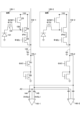
- FIG. 12 is a diagram showing a configuration example of a signal readout circuit for two columns according to an eighth embodiment.
- FIG. 12 is a diagram showing an example of the configuration of a comparator applied to a signal readout circuit according to an eighth embodiment.
- FIG. 12 is a diagram showing an example of waveforms of various parts during signal readout of the imaging device according to the eighth embodiment.
- FIG. 12 is a diagram showing an example of waveforms of various parts during signal readout of an imaging device according to a comparative example of the eighth embodiment.
- FIG. 12 is a diagram showing an example of the configuration of a signal readout circuit for one column according to a ninth embodiment.
- 10 is a diagram showing an example of the configuration of a signal readout circuit for one column according to a tenth embodiment.
- FIG. 12 is a perspective view showing a configuration example of an imaging device according to an eleventh embodiment.
- FIG. 1 is a block diagram showing a schematic configuration example of a vehicle control system.
- FIG. 3 is an explanatory diagram showing an example of an installation position of an imaging unit.
- First embodiment (example in which a signal line clip transistor is connected via a signal line clip selection transistor electrically connected to a vertical signal line) 2.
- Second embodiment an example in which a signal line clipping transistor and a signal line clipping selection transistor are provided in an upper layer chip in which pixels are provided, and a signal line clipping voltage setting section is provided in a lower layer chip) 3.
- Third embodiment (example in which a driver that drives a signal line clip selection transistor and a driver that drives a signal line reset transistor are provided) 4.
- Fourth embodiment (example in which a constant current transistor is connected in parallel to a series circuit of a signal line reset transistor and a diode-connected transistor) 5.
- Fifth embodiment (example in which clipping the potential of a signal line and selecting a selected signal line are performed using a signal line clipping transistor) 6.
- Sixth embodiment (example where an amplification transistor of an OB (Optical Black) pixel is used as a signal line clipping transistor and a selection transistor of an OB pixel is used as a signal line clipping selection transistor) 7.
- Seventh embodiment (example where a resistance ladder circuit is used to set the clip level of a signal line and also to set the reset level of a signal line) 8.
- FIG. 1 is a block diagram showing a configuration example of a camera to which an imaging device according to a first embodiment is applied.
- a camera 100 includes an optical system 101, a solid-state imaging device 102, an imaging control section 103, an image processing section 104, a storage section 105, a display section 106, and an operation section 107.
- the imaging control section 103, the image processing section 104, the storage section 105, the display section 106, and the operation section 107 are connected to each other via a bus 108.
- the camera 100 may be used alone, or may be incorporated into a mobile terminal such as a smartphone, or may be incorporated into an authentication device or a monitoring device.
- the optical system 101 makes light from a subject enter the solid-state imaging device 102 and forms an image of the subject on the light-receiving surface of the solid-state imaging device 102.
- the optical system 101 can include, for example, a focus lens, a zoom lens, an aperture, and the like.
- Optical system 101 may include multiple lenses such as a wide-angle lens, a standard lens, and a telephoto lens.
- the solid-state imaging device 102 converts light from a subject into an electrical signal for each pixel, digitizes the electrical signal, and outputs the digital signal.
- the solid-state imaging device 102 may be, for example, a CMOS (Complementary Metal Oxide Semiconductor) image sensor or a CCD (Charge Coupled Device).
- CMOS Complementary Metal Oxide Semiconductor
- CCD Charge Coupled Device
- the imaging control unit 103 controls imaging by the solid-state imaging device 102 based on commands from the operation unit 107. At this time, the imaging control unit 103 can control the exposure time, exposure amount, imaging timing, etc. of the solid-state imaging device 102.
- the image processing unit 104 performs image processing based on the output from the solid-state imaging device 102.
- Image processing includes, for example, gamma correction, white balance processing, sharpness processing, and gradation conversion processing.
- the image processing unit 104 may include a processor that executes processing based on software.
- the storage unit 105 stores captured images captured by the solid-state imaging device 102, and stores imaging parameters of the solid-state imaging device 102. Furthermore, the storage unit 105 can store a program for operating the camera 100 based on software.
- the storage unit 105 may include a ROM (Read Only Memory), a RAM (Random Access Memory), and a memory card.
- the display unit 106 displays captured images and various information that supports imaging operations.
- the display unit 106 may be a liquid crystal display or an organic EL (Electro Luminescence) display.
- the operation unit 107 provides a user interface for operating the camera 100.
- the operation unit 107 may include, for example, buttons, dials, and switches provided on the camera 100.
- the operation unit 107 may be configured with a touch panel together with the display unit 106.
- FIG. 2 is a block diagram showing a configuration example of the solid-state imaging device according to the first embodiment.
- the solid-state imaging device 102 includes a pixel array section 111, a vertical scanning circuit 112, a column readout circuit 113, a column signal processing section 114, a horizontal scanning circuit 115, a control circuit 116, and a signal line clip level setting circuit 117.
- the pixel array section 111 includes a plurality of pixels 120.
- the pixels 120 are arranged in a matrix along the row direction (also referred to as the horizontal direction) and the column direction (also referred to as the vertical direction).
- Each pixel 120 can form a source follower with the column readout circuit 113 during signal readout.
- Each pixel 120 is connected to a horizontal drive line 131 for each row and to a vertical signal line 132 for each column.
- the horizontal drive line 131 drives each pixel 120 row by row when reading signals from each pixel 120.
- the vertical signal line 132 transmits to the column signal processing unit 114 for each column a potential based on accumulated charges according to a current flowing when reading a signal from the pixel 120. Note that the vertical signal line 132 is an example of a signal line described in the claims.
- the vertical scanning circuit 112 scans the pixels 120 to be read in the column direction.
- the vertical scanning circuit 112 may be configured using vertical registers.
- the column readout circuit 113 can form a source follower with each pixel 120 when reading signals from each pixel 120. At this time, the column readout circuit 113 can change the potential of the vertical signal line 132 based on the charge held in the pixel 120. Column readout circuit 113 can support capacitive load readout. The column readout circuit 113 may also support constant current readout. Further, the column read circuit 113 sets the potential of the vertical signal line 132 to the clip level during P-phase VSL settling for capacitive load read. This clip level can be set to a potential higher than the potential of the vertical signal line 132 when reading a signal from the pixel 120 when charge overflows from the photodiode to the floating diffusion. Further, the column readout circuit 113 may set the potential of the vertical signal line 132 to the clip level even during P-phase VSL settling of constant current readout.
- the column signal processing unit 114 processes signals transmitted from each pixel 120 in the column direction. For example, the column signal processing unit 114 can perform correlated double sampling (CDS) processing based on signals transmitted from each pixel 120 in the column direction. Further, the column signal processing unit 114 can perform AD (Analog to Digital) conversion processing based on the signals transmitted in the column direction from each pixel 120, and output the image pickup signal Gout.
- CDS correlated double sampling
- AD Analog to Digital
- the horizontal scanning circuit 115 scans the pixels 120 to be read in the row direction.
- the horizontal scanning circuit 115 may be configured using a horizontal register.
- the control circuit 116 controls the vertical scanning circuit 112, the column readout circuit 113, the column signal processing section 114, and the horizontal scanning circuit 115.
- the control circuit 116 can control the scan timing in the column direction, the scan timing in the row direction, the operation timing of the column readout circuit 113, and the processing timing of the column signal processing section 114.
- the signal line clip level setting circuit 117 sets the signal line clip voltage Vb used to generate the clip level of the potential of the vertical signal line 132.
- the signal line clipping voltage Vb is supplied to the column readout circuit 113 and used to generate a clip level of the potential of the vertical signal line 132.
- the signal line clip level setting circuit 117 may be used to generate a reset level of the potential of the vertical signal line 132.
- FIG. 3 is a block diagram showing an example of a circuit configuration of a pixel provided in the solid-state imaging device according to the first embodiment.
- a pixel 120 includes a photodiode 121, a transfer transistor 122, a reset transistor 123, an amplification transistor 124, a selection transistor 125, and a floating diffusion 126.
- MOS Metal Oxide Semiconductor
- the amplification transistor 124 and the selection transistor 125 are connected in series.
- a cathode of the photodiode 121 is connected to a floating diffusion 126 via a transfer transistor 122.
- the floating diffusion 126 is connected to the power supply Vdd via the reset transistor 123.
- the power supply Vdd is connected to the vertical signal line 132 via a series circuit of an amplification transistor 124 and a selection transistor 125.
- the gate of amplification transistor 124 is connected to floating diffusion 126 .
- a transfer signal ⁇ TG is applied to the gate of the transfer transistor 122.
- a pixel reset signal ⁇ PRT is applied to the gate of the reset transistor 123.
- a selection signal ⁇ SEL is applied to the gate of the selection transistor 125.
- the transfer signal ⁇ TG, pixel reset signal ⁇ PRT, and selection signal ⁇ SEL can be transmitted to each pixel 120 via the horizontal drive line 131 in FIG.
- the transfer transistor 122 When the transfer transistor 122 is turned on, the charges accumulated in the photodiode 121 are transferred to the floating diffusion 126. Then, when the selection transistor 125 is turned on, the source potential of the amplification transistor 124 changes according to the potential of the floating diffusion 126. The source potential of the amplification transistor 124 is applied to the vertical signal line 132 via the selection transistor 125 and transmitted via the vertical signal line 132. Further, when the reset transistor 123 is turned on, the charges accumulated in the floating diffusion 126 are discharged.
- FIG. 4 is a cross-sectional view showing an example of the configuration of a pixel array section provided in the solid-state imaging device according to the first embodiment. Note that FIG. 4 shows an example of a front-illuminated solid-state imaging device. Further, FIG. 4 shows a configuration example for three pixels.
- a photodiode 232 is formed on a semiconductor substrate 231 for each pixel 120.
- the material of the semiconductor substrate 231 may be Si, InGaAs, or InP.
- a gate electrode 214 and a wiring layer 210 are formed on the semiconductor substrate 231.
- Gate electrode 214 is formed on semiconductor substrate 231 with gate insulating film 213 interposed therebetween.
- a sidewall 215 is formed on the sidewall of the gate electrode 214 .
- the material of the gate electrode 214 for example, polycrystalline silicon into which impurities are introduced can be used.
- the material of the gate insulating film 213, for example, a silicon oxide film can be used.
- the gate electrode 214 can be used for a pixel transistor.
- the pixel transistors include the transfer transistor 122, reset transistor 123, amplification transistor 124, and selection transistor 125 in FIG.
- a wiring 216 is formed on the gate electrode 214.
- FIG. 4 shows an example of three-layer wiring.
- the wiring 216 is provided with an opening OP1 that allows light to enter the photodiode 232.
- Gate electrode 214 and wiring 216 are insulated via insulating layer 217.
- insulating layer 217 For example, a silicon oxide film can be used as the insulating layer 217.
- metal such as Al or Cu can be used as the material of the wiring 216.
- a color filter 218 is formed on the wiring layer 210 for each pixel 120.
- a microlens 219 is formed on the color filter 218 for each pixel 120.
- transparent resin such as acrylic or polycarbonate can be used.
- a pigment may be added to the color filter 218 for coloring.
- the color filter 218 can have a Bayer array, for example.
- FIG. 5 is a cross-sectional view showing a modification of the pixel array section provided in the solid-state imaging device according to the first embodiment. Note that FIG. 5 shows an example of a back-illuminated solid-state imaging device. Further, FIG. 5 shows a configuration example for three pixels.
- a photodiode 222 is formed in a semiconductor layer 221 for each pixel 120.
- the material of the semiconductor layer 221 may be Si, InGaAs, or InP.
- the semiconductor layer 221 can be formed, for example, by thinning a semiconductor substrate on which the photodiode 222 is formed from the back side.
- a gate electrode 224 and a wiring layer 220 are formed on the semiconductor layer 221.
- Gate electrode 224 is formed on semiconductor layer 221 with gate insulating film 223 interposed therebetween.
- a sidewall 225 is formed on the sidewall of the gate electrode 224 .
- the gate electrode 224 can be used for a pixel transistor.
- the pixel transistors include the transfer transistor 122, reset transistor 123, amplification transistor 124, and selection transistor 125 in FIG.
- a wiring 226 is formed on the gate electrode 224.
- FIG. 5 shows an example of three-layer wiring. Gate electrode 224 and wiring 226 are insulated via insulating layer 227.
- the semiconductor layer 221 is supported on a support substrate 230 with an insulating layer 227 interposed therebetween.
- the support substrate 230 may be a glass substrate, a Si substrate, or a sapphire substrate.
- a color filter 228 is formed for each pixel 120 on the back side of the semiconductor layer 221.
- a microlens 229 is formed on the color filter 228 for each pixel 120.
- the color filter 228 can have a Bayer array, for example.
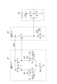
- FIG. 6 is a diagram showing a configuration example of a signal readout circuit for one column according to the first embodiment.
- an amplification transistor 124 is connected to a vertical signal line 132 via a selection transistor 125. Further, a capacitor 133 is added to the vertical signal line 132. This capacitance 133 may be a parasitic capacitance of the vertical signal line 132 or a capacitive element connected to the vertical signal line 132.
- a signal line reset transistor 141 is electrically connected to the vertical signal line 132.
- the signal line reset transistor 141 can reset the potential VSL of the vertical signal line 132.
- a MOS transistor can be used as the signal line reset transistor 141.
- a signal line reset signal ⁇ RT is applied to the gate of the signal line reset transistor 141.
- a diode-connected transistor 142 is connected in series to the signal line reset transistor 141.
- a MOS transistor can be used as the diode-connected transistor 142.
- the gate of diode-connected transistor 142 is connected to the drain of diode-connected transistor 142.
- the source of diode-connected transistor 142 is grounded.
- the source of diode-connected transistor 142 may be connected to a potential higher than ground potential.
- the diode-connected transistor 142 can generate a voltage higher than 0V (for example, 0.5V), and can set the potential VSL of the vertical signal line 132 to a potential higher than 0V via the signal line reset transistor 141.
- the diode-connected transistor 142 is an example of a signal line reset level generation section described in the claims.
- a signal line clip transistor 146 is electrically connected to the vertical signal line 132.
- the signal line clipping transistor 146 clips the potential VSL of the vertical signal line 132.
- a MOS transistor can be used as the signal line clip transistor 146.
- a signal line clipping voltage Vb is applied to the gate of the signal line clipping transistor 146.
- Signal line clip transistor 146 can generate clip level Vcp based on signal line clip voltage Vb.
- the signal line clipping voltage Vb can be lower than the reset level of the pixel 120.
- a signal line clip selection transistor 147 is connected between the signal line clip transistor 146 and the vertical signal line 132.
- the signal line clip selection transistor 147 applies the clip level Vcp generated by the signal line clip transistor 146 to the vertical signal line 132.
- a plurality of clip levels Vcp may be provided and switchable.
- a MOS transistor can be used as the signal line clip selection transistor 147.
- a signal line clip selection signal ⁇ SUN is applied to the gate of the signal line clip selection transistor 147.
- the resistance ladder circuit 155 generates the signal line clip voltage Vb in stages.
- the resistance ladder circuit 155 includes voltage dividing resistors 151 to 154. Voltage dividing resistors 151 to 154 are connected in series with each other.
- the selector 150 switches the divided voltages generated by the voltage dividing resistors 151 to 154, and inputs the divided voltage to the gate of the signal line clipping transistor 146 as the signal line clipping voltage Vb.
- the selector 150 and the resistance ladder circuit 155 are examples of a signal line clip voltage setting section described in the claims.
- FIG. 6 shows an example in which the signal line clipping voltage Vb can be switched to three levels, the number is not necessarily limited to three levels, and may be, for example, two levels or four or more levels.
- the vertical signal line 132 is connected to an inverting input of a comparator 143 via a DC cut capacitor 144. At this time, the potential VSL of the vertical signal line 132 is applied to the inverting input of the comparator 143 via the DC cut capacitor 144.
- a reference signal RAP is input to a non-inverting input of the comparator 143 via a DC cut capacitor 145. Reference signal RAP is, for example, a ramp signal. Further, the auto-zero signal AZ is input to the comparator 143.
- the auto-zero control unit 148 inputs the auto-zero signal AZ to the comparator 143.
- the autozero signal AZ activates autozero operation during the autozero period.
- the auto-zero control unit 148 can control the charge accumulated in each DC cut capacitor 144 and 145 so that the non-inverting input and the inverting input of the comparator 143 are balanced.
- the potential VSL of the vertical signal line 132 is set to a potential higher than 0V. Then, after the signal line reset transistor 141 is turned off, the selection transistor 125 and the signal line clip selection transistor 147 are turned on. At this time, when high-intensity light such as sunlight enters the pixel 120, the potential VSL of the vertical signal line 132 is clipped to the clip level Vcp by the signal line clip transistor 146 during P-phase VSL settling of capacitive load readout. be done.
- the potential can be set higher than the potential of the vertical signal line 132 when reading signals from the pixel 120.
- the comparator 143 compares the potential VSL of the vertical signal line 132 with the reference signal RAP, and outputs the comparison result COP.
- the potential VSL of the vertical signal line 132 is clipped to the clip level Vcp during P-phase VSL settling for capacitive load readout, so sunspot phenomena can be prevented.
- the potential VSL of the vertical signal line 132 is such that the electric charge corresponding to the pixel current IPX flowing to the vertical signal line 132 via the selection transistor 125 is accumulated in the capacitor 133.
- the potential VSL of the vertical signal line 132 changes based on the charge accumulated in the capacitor 133.
- the comparator 143 compares the potential VSL of the vertical signal line 132 with the reference signal RAP, and outputs the comparison result COP.
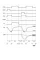
- FIG. 7 is a diagram showing a first example of waveforms of each part during signal readout of the imaging device according to the first embodiment. Note that this figure shows the waveforms of various parts during signal readout when high-intensity light such as sunlight is incident on the pixel 120.
- pixel reset/VSL reset is performed in capacitive load readout of the imaging device (K11).
- the pixel reset signal ⁇ PRT rises (t11)
- the reset transistor 123 is turned on
- the floating diffusion 126 is reset.
- the reset level of the floating diffusion 126 can be set to the power supply potential Vdd.
- the signal line reset signal ⁇ RT rises (t11)
- the signal line reset transistor 141 is turned on, and the vertical signal line 132 is reset.
- the reset level of the vertical signal line 132 is set to a potential higher than 0V (for example, 0.5V) by the forward voltage VR of the diode-connected transistor 142.
- 0V for example, 0.5V
- the rising timing of the pixel reset signal ⁇ PRT and the rising timing of the signal line reset signal ⁇ RT do not necessarily have to be simultaneous, and may be shifted from each other.
- the fall timing of the signal line reset signal ⁇ RT does not need to be later than the fall timing of the pixel reset signal ⁇ PRT, and is not particularly limited as long as it is before the rise of the selection signal ⁇ SEL.
- P-phase VSL settling is performed (K12).
- the signal line reset signal ⁇ RT falls, the selection signal ⁇ SEL rises (t12), and the selection transistor 125 is turned on.
- the output of the resistance ladder circuit 155 is selected so that the signal line clipping voltage Vb is lower than the reset level of the pixel 120, and is applied to the gate of the signal line clipping transistor 146.
- the signal line clip selection signal ⁇ SUN rises (t12)
- the signal line clip selection transistor 147 turns on
- the auto-zero signal AZ rises (t12), activating the auto-zero operation of the comparator 143.
- the signal line clip selection signal ⁇ SUN falls (t14).
- the potential VSL of the vertical signal line 132 is clipped to the clip level Vcp, and the non-inverting input and the inverting input of the comparator 143 are adjusted so as to be balanced when the potential VSL of the vertical signal line 132 is clipped. .
- P-phase AD is performed (K13).
- the ramp signal is supplied to the comparator 143 as the reference signal RAP.
- the potential VSL of the vertical signal line 132 according to the clip level Vcp is compared with the reference signal RAP, and the timing when the level of the reference signal RAP matches the potential VSL of the vertical signal line 132 is the comparison result COP. is output as
- the clip level Vcp set to the vertical signal line 132 is AD converted based on a counting operation until the level of the reference signal RAP matches the potential VSL of the vertical signal line 132.
- transfer/VSL reset is performed (K14).
- the transfer signal ⁇ TG rises (t15)
- the transfer transistor 122 is turned on, and the charges accumulated in the photodiode 121 are transferred to the floating diffusion 126.
- the signal line reset signal ⁇ RT rises (t15)
- the signal line reset transistor 141 is turned on, and the vertical signal line 132 is reset.
- the reset level of the vertical signal line 132 is set to a potential higher than 0V (for example, 0.5V) by the forward voltage VR of the diode-connected transistor 142.
- the rising timing of the transfer signal ⁇ TG and the rising timing of the signal line reset signal ⁇ RT do not necessarily have to be simultaneous, and may be shifted from each other. Further, the fall timing of the signal line reset signal ⁇ RT does not need to be later than the fall timing of the transfer signal ⁇ TG, and is not particularly limited as long as it is before the rise of the selection signal ⁇ SEL.
- D-phase VSL settling is performed (K15).
- the signal line reset signal ⁇ RT falls, the selection signal ⁇ SEL rises (t16), and the selection transistor 125 is turned on.
- a pixel current IPX corresponding to the signal level of the floating diffusion 126 flows to the vertical signal line 132 via the selection transistor 125.
- charges corresponding to the pixel current IPX are accumulated in the capacitor 133, and the potential VSL of the vertical signal line 132 is set based on the charges accumulated in the capacitor 133.
- D-phase AD is performed (K16).
- the selection signal ⁇ SEL falls (t17), and the ramp signal is supplied to the comparator 143 as the reference signal RAP (t17-t18).
- the comparator 143 the potential VSL of the vertical signal line 132 according to the signal level is compared with the reference signal RAP, and the timing when the level of the reference signal RAP matches the potential VSL of the vertical signal line 132 is determined as the comparison result COP.
- the signal level read from the pixel 120 is AD converted based on a counting operation until the level of the reference signal RAP matches the potential VSL of the vertical signal line 132.
- FIG. 8 is a diagram showing a second example of waveforms of each part during signal readout of the imaging device according to the first embodiment. Note that the same figure shows waveforms of various parts during signal readout when normal light is incident on the pixel 120.
- the signal readout operation when normal light is incident on the pixel 120 is similar to the signal readout operation when high-intensity light such as sunlight is incident on the pixel 120.
- charges do not overflow from the photodiode 121 to the floating diffusion 126 during P-phase VSL settling (K12).
- the selection transistor 125 is turned on, a pixel current IPX corresponding to the reset level of the floating diffusion 126 flows to the vertical signal line 132 via the selection transistor 125 based on the source follower operation of the amplification transistor 124.
- the signal line clip transistor 146 is electrically connected via the signal line clip selection transistor 147 connected to the vertical signal line 132.
- the potential VSL of the vertical signal line 132 can be clipped without depending on the amount of incident light, making it possible to prevent sunspot phenomena and speeding up P-phase VSL settling.
- the signal line clipping transistor 146 is electrically connected via the signal line clipping selection transistor 147 connected to the vertical signal line 132.
- a signal line clipping transistor 146 and a signal line clipping selection transistor 147 are provided on the upper layer chip in which the pixel 120 is provided, and a resistance ladder circuit 155 and a selector 150 are provided on the lower layer chip.
- FIG. 9 is a diagram showing a configuration example of a signal readout circuit for one column according to the second embodiment.
- this signal readout circuit is similar to the circuit configuration of the signal readout circuit in FIG. However, this signal readout circuit is formed on a stacked chip.
- This stacked chip includes an upper layer chip 161 and a lower layer chip 162.
- Upper layer chip 161 is stacked on lower layer chip 162.
- a pixel 120, a vertical signal line 132, a signal line clip transistor 146, and a signal line clip selection transistor 147 are formed on the upper layer chip 161.
- the gate length and gate width of the signal line clip transistor 146 can be made equal to the gate length and gate width of the amplification transistor 124 of the pixel 120.
- the gate length and gate width of the signal line clip selection transistor 147 can be made equal to the gate length and gate width of the selection transistor 125 of the pixel 120.
- a signal line reset transistor 141, a diode-connected transistor 142, a comparator 143, a resistance ladder circuit 155, and a selector 150 are formed in the lower chip 162. At this time, the vertical signal line 132 can be wired from the upper layer chip 161 to the lower layer chip 162.
- the signal line clip transistor 146 and the signal line clip selection transistor 147 are formed in the upper layer chip 161 on which the pixel 120 is formed. This makes it possible to equalize the characteristic variations of the pixel transistors provided in the pixel 120 and the characteristic variations of the signal line clip transistor 146 and the signal line clip selection transistor 147.
- the signal line clipping transistor 146 is electrically connected via the signal line clipping selection transistor 147 connected to the vertical signal line 132.
- a driver for driving the signal line clip selection transistor 147 and a driver for driving the signal line reset transistor 141 are provided in the peripheral circuit of the pixel 120.
- FIG. 10 is a diagram showing a configuration example of a signal readout circuit for three columns according to the third embodiment.
- a signal line reset transistor 141 a diode-connected transistor 142, a comparator 143, a signal line clip transistor 146, and a signal line clip selection transistor 147 are provided for each column.
- the driver 161 drives the signal line clip selection transistor 147.
- the driver 162 drives the signal line reset transistor 141.
- Drivers 161 and 162 are provided in the peripheral circuit of pixel 120.
- the driver 161 is shared by a plurality of signal line clip selection transistors 147 having different columns.
- the driver 162 is shared by a plurality of signal line reset transistors 141 having different columns.
- the resistance ladder circuit 155 and the selector 150 are shared by a plurality of signal line clip transistors 146 having different columns.
- the driver 161 is shared by a plurality of signal line clip selection transistors 147 in different columns, and the driver 162 is shared by a plurality of signal line reset transistors 141 in different columns. . This makes it possible to prevent the sunspot phenomenon during capacitive load reading while suppressing an increase in the area occupied by the drivers 161 and 162.
- the clipping operation of the potential VSL of the vertical signal line 132 during P-phase VSL settling is applied to capacitive load reading.
- FIG. 11 is a diagram showing a configuration example of a signal readout circuit for one column according to the fourth embodiment.
- this signal readout circuit has a sample hold circuit 201 and a constant current transistor 301 added to the signal readout circuit of the first embodiment described above.
- the other configuration of the signal readout circuit of the fourth embodiment is similar to the configuration of the signal readout circuit of the first embodiment described above.
- the sample and hold circuit 201 samples and holds the bias voltage Vbs that operates the constant current transistor 301, and applies it to the gate of the constant current transistor 301.
- Sample and hold circuit 201 includes a transistor 211 and a capacitor 212.
- Transistor 211 may be a MOS transistor.
- a sample and hold signal ⁇ SH is applied to the gate of the transistor 211.
- Capacitor 212 is connected between the source of transistor 211 and ground potential.
- Constant current transistor 301 is electrically connected to the vertical signal line 132.
- Constant current transistor 301 may be a MOS transistor.
- the bias voltage Vbs is set to 0V and the sample hold signal ⁇ SH is set to high level.
- the constant current transistor 301 is turned off, and no current flows through the constant current transistor 301.
- the operation of the signal readout circuit at this time is similar to that in FIG. 7 or 8.
- the transistor 211 In constant current reading, the transistor 211 is turned on and the bias voltage Vbs is sampled and held. Then, the transistor 211 is turned off, and the bias voltage Vbs sampled and held by the sample and hold circuit 201 is applied to the gate of the constant current transistor 301. In this case, the constant current transistor 301 is turned on, and a constant current flows through the constant current transistor 301.
- FIG. 12 is a diagram showing an example of waveforms of various parts during constant current readout of the signal readout circuit according to the fourth embodiment. Note that this figure shows the waveforms of various parts during signal readout when high-intensity light such as sunlight is incident on the pixel 120.
- the transistor 211 in constant current readout, the transistor 211 is turned on and the bias voltage Vbs is sampled and held in order to prevent horizontal scanning noise during AD conversion. Then, the transistor 211 is turned off, and the bias voltage Vbs sampled and held by the sample and hold circuit 201 is applied to the gate of the constant current transistor 301.
- pixel reset is performed (K21).
- the pixel reset signal ⁇ PRT rises (t21)
- the reset transistor 123 is turned on
- the floating diffusion 126 is reset.
- the selection signal ⁇ SEL rises (t21)
- the selection transistor 125 is turned on.
- the potential VSL of the vertical signal line 132 is set based on the source follower operation when the power supply potential Vdd is applied to the gate of the amplification transistor 124.
- P-phase VSL settling is performed (K22).
- the pixel reset signal ⁇ PRT falls (t22), and the reset transistor 123 is turned off.
- the potential VSL of the vertical signal line 132 changes based on the source follower operation when the reset level of the floating diffusion 126 is applied to the gate of the amplification transistor 124.
- a signal line clipping voltage Vb set to be lower than the reset level of the pixel 120 is applied to the gate of the signal line clipping transistor 146.
- the signal line clip selection signal ⁇ SUN rises (t23), the signal line clip selection transistor 147 turns on, and the auto-zero signal AZ rises (t23), activating the auto-zero operation of the comparator 143.
- the signal line clip selection signal ⁇ SUN falls (t24).
- the potential VSL of the vertical signal line 132 is clipped to the clip level Vcp, and the non-inverting input and the inverting input of the comparator 143 are adjusted so as to be balanced when the potential VSL of the vertical signal line 132 is clipped. .
- P-phase AD is performed (K23).
- the ramp signal is supplied to the comparator 143 as the reference signal RAP.
- the potential VSL of the vertical signal line 132 according to the clip level Vcp is compared with the reference signal RAP, and the timing when the level of the reference signal RAP matches the potential VSL of the vertical signal line 132 is the comparison result COP. is output as
- the clip level Vcp set to the vertical signal line 132 is AD converted based on a counting operation until the level of the reference signal RAP matches the potential VSL of the vertical signal line 132.
- transfer is performed (K24).
- the transfer signal ⁇ TG rises (t25)
- the transfer transistor 122 is turned on, and the charges accumulated in the photodiode 121 are transferred to the floating diffusion 126.
- the potential VSL of the vertical signal line 132 is set based on the source follower operation when the cathode potential of the photodiode 121 is applied to the gate of the amplification transistor 124.
- D-phase VSL settling is performed (K25).
- the transfer signal ⁇ TG falls (t25) and the transfer transistor 122 is turned off.
- the potential VSL of the vertical signal line 132 is set based on the source follower operation when the signal level of the floating diffusion 126 is applied to the gate of the amplification transistor 124.
- P-phase AD is performed (K26).
- the ramp signal is supplied to the comparator 143 as the reference signal RAP (t27-t28).
- the potential VSL of the vertical signal line 132 according to the signal level is compared with the reference signal RAP, and the timing when the level of the reference signal RAP matches the potential VSL of the vertical signal line 132 is determined as the comparison result COP.
- the signal level read from the pixel 120 is AD converted based on a counting operation until the level of the reference signal RAP matches the potential VSL of the vertical signal line 132.
- the constant current transistor 301 is connected in parallel to the series circuit of the signal line reset transistor 141 and the diode-connected transistor 142, and the vertical signal line 132 is Clip the potential VSL. This makes it possible to switch between constant current readout and capacitive load readout while preventing the sunspot phenomenon.
- the signal line clip transistor 146 is electrically connected via the signal line clip selection transistor 147 connected to the vertical signal line 132.
- a signal line clipping transistor 146 performs clipping of the potential VSL of the vertical signal line 132 and selection of the vertical signal line 132.
- FIG. 13 is a diagram showing a configuration example of a signal readout circuit for one column according to the fifth embodiment.
- this signal readout circuit has the signal line clip selection transistor 147 removed from the signal readout circuit of the first embodiment described above.
- the rest of the configuration of the signal readout circuit of the fifth embodiment is similar to the configuration of the signal readout circuit of the first embodiment described above.
- the signal line clipping transistor 146 is directly connected to the vertical signal line 132. At this time, the signal line clipping transistor 146 clips the potential VSL of the vertical signal line 132 and selects the vertical signal line 132 instead of the signal line clipping selection transistor 147.
- FIG. 14 is a diagram showing an example of waveforms of various parts during constant current readout of the signal readout circuit according to the fifth embodiment. Note that this figure shows the waveforms of various parts during signal readout when high-intensity light such as sunlight is incident on the pixel 120.
- the operation when the signal line clip selection transistor 147 is not present is the same as the operation when the signal line clip selection transistor 147 is present.
- the signal line clipping voltage Vb changes from voltage Vb1 to voltage Vb2 based on the switching operation of the selector 150, and is applied to the gate of the signal line clipping transistor 146 (t12).
- the signal line clipping voltage Vb transitions from the voltage Vb2 to the voltage Vb1, and is applied to the gate of the signal line clipping transistor 146 (t14).
- Voltage Vb1 is set so that signal line clip transistor 146 is turned off.
- Voltage Vb2 is set so that potential VSL of vertical signal line 132 clipped via signal line clipping transistor 146 matches clip level Vcp.
- clipping of the potential VSL of the vertical signal line 132 and selection of the vertical signal line 132 are performed by the signal line clipping transistor 146.
- the signal line clip selection transistor 147 can be omitted, and the circuit configuration can be simplified.
- the signal line clipping transistor 146 is electrically connected via the signal line clipping selection transistor 147 connected to the vertical signal line 132.
- the amplification transistor of the OB pixel is used as the signal line clipping transistor 146, and the selection transistor of the OB pixel is used as the signal line clipping selection transistor 147.
- FIG. 15 is a diagram showing a configuration example of a signal readout circuit for one column according to the sixth embodiment.
- this signal readout circuit is provided with an OB pixel 400 in place of the signal line clipping transistor 146 and the signal line clipping selection transistor 147 of the above-described first embodiment.
- the other configuration of the signal readout circuit of the fourth embodiment is similar to the configuration of the signal readout circuit of the first embodiment described above.
- the OB pixel 400 includes a photodiode 421, a transfer transistor 422, a reset transistor 423, an amplification transistor 424, a selection transistor 425, and a floating diffusion 426.
- Photodiode 421 is covered with a light shielding film.
- the amplification transistor 424 and the selection transistor 425 are connected in series.
- a cathode of the photodiode 421 is connected to a floating diffusion 426 via a transfer transistor 422.
- the power supply Vdd is connected to the vertical signal line 132 via a series circuit of an amplification transistor 424 and a selection transistor 425.
- the gate of amplification transistor 424 is connected to floating diffusion 426 .
- a transfer signal ⁇ TGB is applied to the gate of the transfer transistor 422.
- a pixel reset signal ⁇ PRTS is applied to the gate of the reset transistor 423.
- a signal line clipping voltage Vb is applied to the drain of the reset transistor 423.
- a selection signal ⁇ SELS is applied to the gate of the selection transistor 425.
- the transfer signal ⁇ TGB, the pixel reset signal ⁇ PRTS, and the selection signal ⁇ SELS can be transmitted to the OB pixel 400 via the horizontal drive line 131 in FIG.
- FIG. 16 is a diagram showing an example of waveforms of various parts during constant current readout of the signal readout circuit according to the sixth embodiment. Note that this figure shows the waveforms of various parts during signal readout when high-intensity light such as sunlight is incident on the pixel 120.
- the amplification transistor 424 of the OB pixel 400 is used as the signal line clipping transistor 146, and the selection transistor 425 of the OB pixel 400 is used as the signal line clipping selection transistor 147.
- the capacitive load read operation in this case is similar to the capacitive load read operation in FIG.
- the amplification transistor 424 of the OB pixel 400 is used as the signal line clip transistor 146, the signal line clip voltage Vb is applied to the gate of the amplification transistor 424.
- the pixel reset signal ⁇ PRTS is set to high level (t11-t18), and the reset transistor 423 is turned on.
- the transfer signal ⁇ TGB is set to a low level (t11-t18), and the transfer transistor 422 is turned off.
- the selection signal ⁇ SELS rises (t12), and the selection transistor 425 is turned on. Further, the output of the resistance ladder circuit 155 is selected so that the signal line clip voltage Vb is lower than the reset level of the pixel 120 and is applied to the gate of the amplification transistor 424. Further, the auto-zero signal AZ rises (t12), and the auto-zero operation of the comparator 143 is activated. Then, after the auto-zero signal AZ falls, the selection signal ⁇ SELS falls (t14).
- the potential VSL of the vertical signal line 132 is clipped to the clip level Vcp, and the non-inverting input and the inverting input of the comparator 143 are adjusted so as to be balanced when the potential VSL of the vertical signal line 132 is clipped. .
- the transfer transistor 422, reset transistor 423, amplification transistor 424, and selection transistor 425 of the OB pixel 400 are operated in the same manner as the transfer transistor 122, reset transistor 123, amplification transistor 124, and selection transistor 125 of the pixel 120. Further, the output of the resistance ladder circuit 155 is selected so that the signal line clip voltage Vb is supplied as the power supply Vdd, and is applied to the drain of the reset transistor 423. At this time, the OB pixel 400 is shielded from light and no light enters it, so there is no need to clip the vertical signal line 132 during P-phase VLS settling.
- the amplification transistor 424 of the OB pixel 400 is used as the signal line clipping transistor 146, and the selection transistor 425 of the OB pixel 400 is used as the signal line clipping selection transistor 147.
- the diode-connected transistor 142 in order to set the reset level of the vertical signal line 132, is connected via the signal line reset transistor 141 electrically connected to the vertical signal line 132.
- the resistance ladder circuit 155 is used to set the clip level Vcp of the vertical signal line 132 and also to set the reset level of the vertical signal line 132.
- FIG. 17 is a diagram showing a configuration example of a signal readout circuit for one column according to the seventh embodiment.
- this signal readout circuit is provided with a selector 500 in place of the diode-connected transistor 142 of the first embodiment described above.
- the other configuration of the signal readout circuit of the seventh embodiment is similar to the configuration of the signal readout circuit of the first embodiment described above.
- the selector 500 switches the divided voltages generated by the voltage dividing resistors 151 to 154 and applies the divided voltage to the source of the signal line reset transistor 141 as a reset voltage VRT.
- Reset voltage VRT can be set to a voltage greater than 0V. Switching of selector 500 can be controlled separately from switching of selector 150.
- the resistance ladder circuit 155 is used to set the clip level Vcp of the vertical signal line 132, and is also used to set the reset voltage VRT of the vertical signal line 132. This makes it possible to switch the reset voltage VRT of the vertical signal line 132 while suppressing an increase in circuit scale.
- the signal read from the pixel 120 is detected based on the potential VSL of the vertical signal line 132 while clipping the potential VSL of the vertical signal line 132 during P-phase VSL settling.
- edge detection is performed based on the comparison result of the potential of the vertical signal line based on load capacitance read from different columns.
- FIG. 18 is a diagram showing a configuration example of a signal readout circuit for two columns according to the eighth embodiment.
- this signal readout circuit includes a plurality of vertical signal lines 132-1 and 132-2, and comparators 143-1 and 143-2 in place of the comparator 143 of the first embodiment described above. Be prepared.
- the other configuration of the signal readout circuit of the eighth embodiment is similar to the configuration of the signal readout circuit of the first embodiment described above, and although not shown, the signal line clip transistor 146 and A signal line clip selection transistor 147 may be included.
- Pixels 120-1 and 120-2 are connected to each vertical signal line 132-1 and 132-2, respectively, and vertical signal lines 132-1 and 132-2 are connected to each comparator 143-1 and 143-2. 2 are connected together.
- Each pixel 120-1 and 120-2 can be configured similarly to pixel 120 in FIG. 6.
- Each pixel 120-1 and 120-2 is connected to vertical signal lines 132-1 and 132-2, respectively.
- a diode-connected transistor 142 is connected to each vertical signal line 132-1 and 132-2 via a signal line reset transistor 141.
- Each comparator 143-1 and 143-2 detects a difference between comparator inputs DVSL1 and DVSL2. At this time, the potentials VLS1 and VLS2 of the vertical signal lines 132-1 and 132-2 are outputted via the respective DC cut capacitors 144 and 145, thereby generating the respective comparator inputs DVSL1 and DVSL2. Then, if the difference between comparator inputs DVSL1 and DVSL2 after auto-zero of each comparator 143-1 and 143-2 is equal to or greater than a threshold value, it can be determined that an edge exists.
- FIG. 19 is a diagram showing a configuration example of a comparator applied to the signal readout circuit according to the eighth embodiment.
- the configuration of the comparator 143-1 in FIG. 18 will be taken as an example, but the comparator 143-2 can also be configured in the same way.
- the comparator 143-1 includes a differential amplifier 501, a subsequent stage amplifier 502, and an inverter 503.
- the rear amplifier 502 is connected to the rear of the differential amplifier 501
- the inverter 503 is connected to the rear of the rear amplifier 502.
- the differential amplifier 501 balances the comparator inputs DVSL1 and DVSL2 based on the auto-zero operation, and then outputs a voltage according to the difference between the comparator inputs DVSL1 and DVSL2.
- Differential amplifier 501 includes PMOS transistors 511, 521, 551 and 561 and NMOS transistors 531, 541 and 571.
- the PMOS transistor 511 and the NMOS transistor 531 are connected in series with each other.
- PMOS transistor 521 and NMOS transistor 541 are connected in series with each other.
- the sources of each PMOS transistor 511 and 521 are connected to power supply voltage VDDH, and the gate of each PMOS transistor 511 and 521 is connected to the drain of PMOS transistor 521. At this time, PMOS transistors 511 and 521 can constitute a current mirror.
- a PMOS transistor 551 is connected between the gate and drain of the NMOS transistor 531, and a PMOS transistor 561 is connected between the gate and drain of the NMOS transistor 541.
- the sources of each NMOS transistor 531 and 541 are grounded via NMOS transistor 571.
- An auto-zero signal AZP is applied to the gate of each PMOS transistor 551 and 561, and a bias voltage BIAS is applied to the gate of the NMOS transistor 571.
- NMOS transistor 571 can operate as a constant current source based on bias voltage BIAS.
- Post-stage amplifier 502 amplifies the output of the differential amplifier 501.
- Post-stage amplifier 502 includes a PMOS transistor 512, an NMOS transistor 522, and a switch 532.
- the PMOS transistor 512 and the NMOS transistor 522 are connected in series with each other.
- the source of the PMOS transistor 512 is connected to the power supply voltage VDDH, and the gate of the PMOS transistor 512 is connected to the drain of the PMOS transistor 511.
- a switch 532 is connected between the gate and drain of the NMOS transistor 522, and the source of the NMOS transistor 522 is grounded. Switch 532 opens and closes based on auto-zero signal AZN.
- the inverter 503 converts the output of the subsequent stage amplifier 502 into a logical value '0' or a logical value '1'.
- Inverter 503 includes a PMOS transistor 513 and an NMOS transistor 523.
- the PMOS transistor 513 and the NMOS transistor 523 are connected in series with each other.
- the source of PMOS transistor 513 is connected to power supply voltage VDDL, and the source of NMOS transistor 523 is grounded.
- Power supply voltage VDDL can be lower than power supply voltage VDDH.
- the gate of PMOS transistor 513 and the gate of NMOS transistor 523 are connected to the drain of PMOS transistor 512.
- each PMOS transistor 551 and 561 is turned on based on the auto-zero signal AZP, and the switch 532 is closed based on the auto-zero signal AZN. Note that the timing at which each PMOS transistor 551 and 561 turns off after being turned on can be made later than the timing at which the switch 532 opens after closing. At this time, current flows through each PMOS transistor 551 and 561 based on the current mirror operation of PMOS transistors 511 and 521. Then, charge is accumulated in each DC cut capacitor 144 and 145 so that the non-inverting input and the inverting input of comparator 143-1 are balanced.
- FIG. 20 is a diagram showing an example of waveforms of each part during signal readout of the imaging device according to the eighth embodiment. In the figure, it is assumed that normal light is incident on the pixel 120-1, and high-intensity light such as sunlight is incident on the pixel 120-2.
- the capacitive load readout operation is the same as in FIG. 8 for pixel 120-1, and the same as in FIG. 7 for pixel 120-2.
- the potential VSL2 of the vertical signal line 132-2 is clipped during P-phase VSL settling (K12), so the potential of the vertical signal line 132-2 is Potential VSL2 is raised to a potential equivalent to potential VSL1 of vertical signal line 132-1.
- the difference between the comparator inputs DVSL1 and DVSL2 corresponding to the difference between the potentials VSL1 and VSL2 of each vertical signal line 132-1 and 132-2 is substantially maintained, and erroneous edge determination is prevented.
- FIG. 21 is a diagram illustrating an example of waveforms of various parts during signal readout of an imaging device according to a comparative example of the eighth embodiment.
- the vertical signal line 132-2 is not clipped during P-phase VSL settling.
- normal light is incident on the pixel 120-1, and high-intensity light such as sunlight is incident on the pixel 120-2.
- the capacitive load readout operation is the same as in FIG. 8 for pixel 120-1, and the same as in FIG. 7 for pixel 120-2.
- the signal line clip selection signal ⁇ SUN maintains a low level during P-phase VSL settling (K12).
- the potential VSL2 of the vertical signal line 132-2 is not clipped, if normal light enters the pixel 120-1 and high-intensity light enters the pixel 120-2, each vertical signal line 132 during P-phase VSL settling -1 and 132-2 potentials VSL1 and VSL2 are opened.
- the potentials VLS1 and VLS2 of each vertical signal line 132-1 and 132-2 are clipped in P-phase VSL settling, while the potentials of each comparator 143-1 and 143-2 are clipped. After auto-zero, detect the difference between comparator inputs DVSL1 and DVSL2. Thereby, even when high-intensity light such as sunlight is incident on the pixel 120-2, the edges of the object can be detected while reducing the influence of fixed pattern noise.
- the clipping operation of the potential VLS of the vertical signal line 132 is applied to the capacitive load readout from the pixel 120 in which one photodiode 121 is provided for one amplification transistor 124.
- the clipping operation of the potential VLS of the vertical signal line 132 is applied to capacitive load readout from a cell in which four photodiodes are provided for one amplification transistor 124.
- FIG. 22 is a diagram showing a configuration example of a signal readout circuit for one column according to the ninth embodiment.
- this signal readout circuit is provided with a cell 130 in place of the pixel 120 of the signal readout circuit of the first embodiment described above.
- the rest of the configuration of the signal readout circuit of the ninth embodiment is similar to the configuration of the signal readout circuit of the first embodiment described above.
- the cell 130 includes photodiodes 121-1 to 121-4 and transfer transistors 122-1 to 122-4 instead of the photodiode 121 and transfer transistor 122 of the first embodiment described above.
- the other configuration of the cell 130 of the ninth embodiment is similar to the configuration of the pixel 120 of the first embodiment described above.
- Each photodiode 121-1 to 121-4 can be arranged in two rows and two columns. Each of the photodiodes 121-1 to 121-4 is connected to the floating diffusion 126 via transfer transistors 122-1 to 122-4, respectively. Transfer signals ⁇ TG1 to ⁇ TG4 are applied to the gates of each of the transfer transistors 122-1 to 122-4. By controlling the application timing of the transfer signals ⁇ TG1 to ⁇ TG4, signals can be read out individually from each photodiode 121-1 to 121-4 to the vertical signal line 132.
- the capacitive load reading operation from each photodiode 121-1 to 121-4 is similar to that in FIG. 7 or 8.
- the vertical signal line 132 is used for capacitive load reading from the cell 130 in which four photodiodes 121-1 to 121-4 are provided for one amplification transistor 124.
- a clipping operation of the potential VLS is applied.
- the clipping operation of the potential VLS of the vertical signal line 132 is applied to the capacitive load reading from each pixel 120 connected to the vertical signal line 132.
- the clipping operation of the potential VLS of the vertical signal line 132 is applied to the binning operation based on capacitive load readout from the pixel 120 connected to the vertical signal line 132.
- FIG. 23 is a diagram showing a configuration example of a signal readout circuit for one column according to the tenth embodiment.
- this signal readout circuit is provided with pixels 140 and 150 in place of the pixel 120 of the signal readout circuit of the first embodiment described above. Further, in this signal readout circuit, a binning line 134 is added to the signal readout circuit of the first embodiment described above. The rest of the configuration of the signal readout circuit of the tenth embodiment is similar to the configuration of the signal readout circuit of the first embodiment described above.
- Each pixel 140 and 150 has a binning transistor 127 added to the pixel 120 of the first embodiment described above.
- the other configurations of each pixel 140 and 150 in the tenth embodiment are similar to the configuration of the pixel 120 in the first embodiment described above.
- a binning transistor 127 is connected between the floating diffusion 126 and the binning line 134 for each pixel 140 and 150.
- Binning transistor 127 may be a MOS transistor.
- Binning signals ⁇ BN1 and ⁇ BN2 are applied to the gate of the binning transistor 127 for each pixel 140 and 150.
- Transfer signals ⁇ TG1 and ⁇ TG2 are applied to the gate of the transfer transistor 122 for each pixel 140 and 150.
- Pixel reset signals ⁇ PRT1 and ⁇ PRT2 are applied to the gate of the reset transistor 123 for each pixel 140 and 150.
- Selection signals ⁇ SEL1 and ⁇ SEL2 are applied to the gate of the selection transistor 125 for each pixel 140 and 150.
- each binning signal ⁇ BN1 and ⁇ BN2 When reading signals from each pixel 140 and 150 individually, each binning signal ⁇ BN1 and ⁇ BN2 is set to low level, and the binning transistor 127 of each pixel 140 and 150 is turned off. When reading signals from each pixel 140 and 150 by binning, each binning signal ⁇ BN1 and ⁇ BN2 is set to a high level, and the binning transistor 127 of each pixel 140 and 150 is turned on.
- the capacitive load readout operation from each pixel 140 and 150 is similar to that in FIG. At this time, in the binning readout, either one of the selection transistors 125 of each pixel 140 and 150 may be turned on, or both of the selection transistors 125 of each pixel 140 and 150 may be turned on.
- the binning transistors 127 are provided in the pixels 140 and 150 connected to the vertical signal line 132. Thereby, capacitive load reading can be applied while reducing the number of times each frame is read, and power consumption can be reduced.
- the signal line clip transistor 146 is electrically connected via the signal line clip selection transistor 147 connected to the vertical signal line 132 that transmits the signal read out from the pixel 120.
- substrates on which a solid-state imaging device including a pixel array section in which pixels 120 are arranged in a matrix are formed are laminated.
- FIG. 24 is a perspective view showing a configuration example of an imaging device according to the eleventh embodiment.
- the solid-state imaging device 901 includes a support substrate 911 and a semiconductor substrate 912.
- a semiconductor substrate 912 is stacked on a support substrate 911.
- a pixel array section 913 and a peripheral circuit 914 are formed on the semiconductor substrate 912.
- a column readout circuit 915 and a column ADC 916 are formed in the peripheral circuit 914.
- the column readout circuit 915 and the column ADC 916 may be formed on both sides of the pixel array section 913 in the column direction.
- the column readout circuit 915 can clip the potential of the vertical signal line during D-phase VSL settling and read out signals from each pixel 120 based on capacitive load readout.
- the signal line reset transistor 141, diode-connected transistor 142, signal line clip transistor 146, and signal line clip selection transistor 147 shown in FIG. 6 may be formed in the column readout circuit 915.
- the column ADC 916 can AD convert signals read out via the column readout circuit 915 for each column.
- the solid-state imaging device 901 can constitute a back-illuminated image sensor.
- the solid-state imaging device 902 includes semiconductor substrates 921 and 922.
- a semiconductor substrate 922 is stacked on the semiconductor substrate 921.
- a pixel array section 923 is formed on the semiconductor substrate 922.
- a peripheral circuit 924 is formed on the semiconductor substrate 922 .
- a column readout circuit 925 and a column ADC 926 are formed.
- the column readout circuit 925 and the column ADC 926 may be formed to correspond to positions on both sides of the pixel array section 923 in the column direction.
- the solid-state imaging device 902 can constitute a back-illuminated image sensor.
- the substrates on which the solid-state imaging devices 901 and 902 are formed are laminated.
- the semiconductor substrates 912 and 922 on which each pixel array section 913 and 923 are formed can be thinned, and a back-illuminated image sensor can be formed. can.
- the technology according to the present disclosure (this technology) can be applied to various products.
- the technology according to the present disclosure may be realized as a device mounted on any type of moving body such as a car, electric vehicle, hybrid electric vehicle, motorcycle, bicycle, personal mobility, airplane, drone, ship, robot, etc. It's okay.
- FIG. 25 is a block diagram showing a schematic configuration example of a vehicle control system, which is an example of a mobile object control system to which the technology according to the present disclosure can be applied.
- the vehicle control system 12000 includes a plurality of electronic control units connected via a communication network 12001.
- the vehicle control system 12000 includes a drive system control unit 12010, a body system control unit 12020, an outside vehicle information detection unit 12030, an inside vehicle information detection unit 12040, and an integrated control unit 12050.
- a microcomputer 12051, an audio/image output section 12052, and an in-vehicle network I/F (interface) 12053 are illustrated.
- the drive system control unit 12010 controls the operation of devices related to the drive system of the vehicle according to various programs.
- the drive system control unit 12010 includes a drive force generation device such as an internal combustion engine or a drive motor that generates drive force for the vehicle, a drive force transmission mechanism that transmits the drive force to wheels, and a drive force transmission mechanism that controls the steering angle of the vehicle. It functions as a control device for a steering mechanism to adjust and a braking device to generate braking force for the vehicle.
- the body system control unit 12020 controls the operations of various devices installed in the vehicle body according to various programs.
- the body system control unit 12020 functions as a keyless entry system, a smart key system, a power window device, or a control device for various lamps such as a headlamp, a back lamp, a brake lamp, a turn signal, or a fog lamp.
- radio waves transmitted from a portable device that replaces a key or signals from various switches may be input to the body control unit 12020.
- the body system control unit 12020 receives input of these radio waves or signals, and controls the door lock device, power window device, lamp, etc. of the vehicle.
- the external information detection unit 12030 detects information external to the vehicle in which the vehicle control system 12000 is mounted.
- an imaging section 12031 is connected to the outside-vehicle information detection unit 12030.
- the vehicle exterior information detection unit 12030 causes the imaging unit 12031 to capture an image of the exterior of the vehicle, and receives the captured image.
- the external information detection unit 12030 may perform object detection processing such as a person, car, obstacle, sign, or text on the road surface or distance detection processing based on the received image.
- the imaging unit 12031 is an optical sensor that receives light and outputs an electrical signal according to the amount of received light.
- the imaging unit 12031 can output the electrical signal as an image or as distance measurement information.
- the light received by the imaging unit 12031 may be visible light or non-visible light such as infrared rays.
- the in-vehicle information detection unit 12040 detects in-vehicle information.
- a driver condition detection section 12041 that detects the condition of the driver is connected to the in-vehicle information detection unit 12040.
- the driver condition detection unit 12041 includes, for example, a camera that images the driver, and the in-vehicle information detection unit 12040 detects the degree of fatigue or concentration of the driver based on the detection information input from the driver condition detection unit 12041. It may be calculated or it may be determined whether the driver is falling asleep.
- the microcomputer 12051 calculates control target values for the driving force generation device, steering mechanism, or braking device based on the information inside and outside the vehicle acquired by the vehicle exterior information detection unit 12030 or the vehicle interior information detection unit 12040, Control commands can be output to 12010.
- the microcomputer 12051 realizes ADAS (Advanced Driver Assistance System) functions, including vehicle collision avoidance or shock mitigation, following distance based on vehicle distance, vehicle speed maintenance, vehicle collision warning, vehicle lane departure warning, etc. It is possible to perform cooperative control for the purpose of ADAS (Advanced Driver Assistance System) functions, including vehicle collision avoidance or shock mitigation, following distance based on vehicle distance, vehicle speed maintenance, vehicle collision warning, vehicle lane departure warning, etc. It is possible to perform cooperative control for the purpose of
- ADAS Advanced Driver Assistance System
- the microcomputer 12051 controls the driving force generating device, steering mechanism, braking device, etc. based on information about the surroundings of the vehicle acquired by the vehicle exterior information detection unit 12030 or the vehicle interior information detection unit 12040. It is possible to perform cooperative control for the purpose of autonomous driving, etc., which does not rely on operation.
- the microcomputer 12051 can output a control command to the body system control unit 12020 based on the information outside the vehicle acquired by the outside information detection unit 12030.
- the microcomputer 12051 controls the headlamps according to the position of the preceding vehicle or oncoming vehicle detected by the vehicle exterior information detection unit 12030, and performs cooperative control for the purpose of preventing glare, such as switching from high beam to low beam. It can be carried out.
- the audio and image output unit 12052 transmits an output signal of at least one of audio and images to an output device that can visually or audibly notify information to the occupants of the vehicle or to the outside of the vehicle.
- an audio speaker 12061, a display section 12062, and an instrument panel 12063 are illustrated as output devices.
- the display unit 12062 may include, for example, at least one of an on-board display and a head-up display.
- FIG. 26 is a diagram showing an example of the installation position of the imaging section 12031.
- the imaging unit 12031 includes imaging units 12101, 12102, 12103, 12104, and 12105.
- the imaging units 12101, 12102, 12103, 12104, and 12105 are provided, for example, at positions such as the front nose, side mirrors, rear bumper, back door, and the top of the windshield inside the vehicle 12100.
- An imaging unit 12101 provided in the front nose and an imaging unit 12105 provided above the windshield inside the vehicle mainly acquire images in front of the vehicle 12100.
- Imaging units 12102 and 12103 provided in the side mirrors mainly capture images of the sides of the vehicle 12100.
- An imaging unit 12104 provided in the rear bumper or back door mainly captures images of the rear of the vehicle 12100.
- the imaging unit 12105 provided above the windshield inside the vehicle is mainly used to detect preceding vehicles, pedestrians, obstacles, traffic lights, traffic signs, lanes, and the like.
- FIG. 26 shows an example of the imaging range of the imaging units 12101 to 12104.
- An imaging range 12111 indicates the imaging range of the imaging unit 12101 provided on the front nose
- imaging ranges 12112 and 12113 indicate imaging ranges of the imaging units 12102 and 12103 provided on the side mirrors, respectively
- an imaging range 12114 shows the imaging range of the imaging unit 12101 provided on the front nose.
- the imaging range of the imaging unit 12104 provided in the rear bumper or back door is shown. For example, by overlapping the image data captured by the imaging units 12101 to 12104, an overhead image of the vehicle 12100 viewed from above can be obtained.
- At least one of the imaging units 12101 to 12104 may have a function of acquiring distance information.
- at least one of the imaging units 12101 to 12104 may be a stereo camera including a plurality of image sensors, or may be an image sensor having pixels for phase difference detection.
- the microcomputer 12051 determines the distance to each three-dimensional object within the imaging ranges 12111 to 12114 and the temporal change in this distance (relative speed with respect to the vehicle 12100) based on the distance information obtained from the imaging units 12101 to 12104. In particular, by determining the three-dimensional object that is closest to the vehicle 12100 on its path and that is traveling at a predetermined speed (for example, 0 km/h or more) in approximately the same direction as the vehicle 12100, it is possible to extract the three-dimensional object as the preceding vehicle. can.
- a predetermined speed for example, 0 km/h or more
- the microcomputer 12051 can set an inter-vehicle distance to be secured in advance in front of the preceding vehicle, and perform automatic brake control (including follow-up stop control), automatic acceleration control (including follow-up start control), and the like. In this way, it is possible to perform cooperative control for the purpose of autonomous driving, etc., in which the vehicle travels autonomously without depending on the driver's operation.
- the microcomputer 12051 transfers three-dimensional object data to other three-dimensional objects such as two-wheeled vehicles, regular vehicles, large vehicles, pedestrians, and utility poles based on the distance information obtained from the imaging units 12101 to 12104. It can be classified and extracted and used for automatic obstacle avoidance. For example, the microcomputer 12051 identifies obstacles around the vehicle 12100 into obstacles that are visible to the driver of the vehicle 12100 and obstacles that are difficult to see. Then, the microcomputer 12051 determines a collision risk indicating the degree of risk of collision with each obstacle, and when the collision risk exceeds a set value and there is a possibility of a collision, the microcomputer 12051 transmits information via the audio speaker 12061 and the display unit 12062. By outputting a warning to the driver via the vehicle control unit 12010 and performing forced deceleration and avoidance steering via the drive system control unit 12010, driving support for collision avoidance can be provided.
- the microcomputer 12051 determines a collision risk indicating the degree of risk of collision with each obstacle, and when the collision risk exceed
- At least one of the imaging units 12101 to 12104 may be an infrared camera that detects infrared rays.
- the microcomputer 12051 can recognize a pedestrian by determining whether the pedestrian is present in the images captured by the imaging units 12101 to 12104.
- pedestrian recognition involves, for example, a procedure for extracting feature points in images captured by the imaging units 12101 to 12104 as infrared cameras, and a pattern matching process is performed on a series of feature points indicating the outline of an object to determine whether it is a pedestrian or not.
- the audio image output unit 12052 creates a rectangular outline for emphasis on the recognized pedestrian.
- the display unit 12062 is controlled to display the .
- the audio image output unit 12052 may control the display unit 12062 to display an icon or the like indicating a pedestrian at a desired position.
- the technology according to the present disclosure can be applied to the imaging unit 12031 among the configurations described above.
- the above-described camera 100 can be applied to the imaging unit 12031.
- the present technology can also have the following configuration.
- a signal line whose potential changes based on the charge accumulated in accordance with the current flowing when reading signals from the pixel; a signal line reset transistor that resets the potential of the signal line; a signal line reset level generation unit that generates a reset level of the potential of the signal line; a signal line clipping transistor that clips the potential of the signal line;
- An imaging device comprising: a signal line clipping voltage setting unit that sets a signal line clipping voltage used to generate a clipping level of the potential of the signal line.
- the pixel is photodiode and a transfer transistor that transfers the charge accumulated in the photodiode to a floating diffusion; a reset transistor that resets the floating diffusion; an amplification transistor that outputs a signal according to the potential of the floating diffusion;
- the imaging device according to (1) or (2) further comprising a selection transistor connected between the amplification transistor and the signal line.
- the signal line reset level generation section includes a diode-connected transistor.
- the gate length and gate width of the signal line clip transistor are equal to the gate length and gate width of the amplification transistor of the pixel,
- the imaging device according to any one of (6) to (8), wherein the signal line is simultaneously driven by the signal line clip selection transistor and the amplification transistor of the pixel.
- the imaging device according to any one of (6) to (9), further comprising a comparator that compares the potential of the signal line and a ramp signal.
- the imaging device according to any one of (6) to (9), further comprising a comparator that compares the potentials of signal lines provided in different columns.
- An imaging device according to claim 1. (16) In constant current reading using the constant current transistor, the constant current transistor is turned on; The imaging device according to (15), wherein the constant current transistor is turned off in capacitive load reading using the signal line reset level generation section. (17) The imaging device according to any one of (1) to (16), wherein the signal line clip voltage setting section generates a plurality of clip levels.
- the signal line clipping voltage setting section includes: resistor ladder circuit, The imaging device according to any one of (1) to (17), and a first selector that switches the divided voltage generated by the resistance ladder circuit.
- the signal line reset level generation section The imaging device according to (18), further comprising a second selector that switches the divided voltage generated by the resistance ladder circuit. (20) comprising a pixel array section in which the pixels are arranged in a matrix in a row direction and a column direction; The signal line is provided for each column, The imaging device according to any one of (1) to (19), wherein the signal line reset transistor and the signal line clip transistor are provided for each of the signal lines.
Landscapes
- Engineering & Computer Science (AREA)
- Multimedia (AREA)
- Signal Processing (AREA)
- Solid State Image Pick-Up Elements (AREA)
- Transforming Light Signals Into Electric Signals (AREA)
Abstract
Description
1.第1の実施の形態(垂直信号線に電気的に接続された信号線クリップ選択トランジスタを介して信号線クリップトランジスタを接続した例)
2.第2の実施の形態(画素が設けられた上層チップに信号線クリップトランジスタおよび信号線クリップ選択トランジスタを設けるとともに、信号線クリップ電圧設定部を下層チップに設けた例)
3.第3の実施の形態(信号線クリップ選択トランジスタを駆動するドライバと、信号線リセットトランジスタを駆動するドライバとを設けた例)
4.第4の実施の形態(信号線リセットトランジスタとダイオード接続トランジスタとの直列回路に並列に定電流トランジスタを接続した例)
5.第5の実施の形態(信号線の電位のクリップおよび選択信号線の選択を信号線クリップトランジスタで実施した例)
6.第6の実施の形態(OB(Optical Black)画素の増幅トランジスタを信号線クリップトランジスタとして用いるとともに、OB画素の選択トランジスタを信号線クリップ選択トランジスタとして用いた例)
7.第7の実施の形態(抵抗ラダー回路を信号線のクリップレベルの設定に用いるとともに、信号線のリセットレベルの設定に用いた例)
8.第8の実施の形態(信号線トランジスタとダイオード接続トランジスタとの直列回路を用いた容量負荷読出しをエッジ検出に適用した例)
9.第9の実施の形態(信号線トランジスタとダイオード接続トランジスタとの直列回路を用いた容量負荷読出しを4個のフォトダイオードで増幅トランジスタが共有されるセルに適用した例)
10.第10の実施の形態(信号線トランジスタとダイオード接続トランジスタとの直列回路を用いた容量負荷読出しをビニング読出しに適用した例)
11.第11の実施の形態(固体撮像装置が形成される基板を積層化した例)
12.移動体への応用例
図1は、第1の実施の形態に係る撮像装置が適用されるカメラの構成例を示すブロック図である。
上述の第1の実施の形態では、垂直信号線132に接続された信号線クリップ選択トランジスタ147を介して信号線クリップトランジスタ146を電気的に接続した。この第2の実施の形態では、画素120が設けられた上層チップに信号線クリップトランジスタ146および信号線クリップ選択トランジスタ147を設け、抵抗ラダー回路155およびセレクタ150を下層チップに設ける。
上述の第1の実施の形態では、垂直信号線132に接続された信号線クリップ選択トランジスタ147を介して信号線クリップトランジスタ146を電気的に接続した。この第3の実施の形態では、信号線クリップ選択トランジスタ147を駆動するドライバと、信号線リセットトランジスタ141を駆動するドライバとを画素120の周辺回路に設ける。
上述の第1の実施の形態では、P相VSLセトリングにおける垂直信号線132の電位VSLのクリップ動作を容量負荷読出しに適用した。この第4の実施の形態では、垂P相VSLセトリングにおける垂直信号線132の電位VSLのクリップ動作を実現しつつ、電流読出しと容量負荷読出しとを切替可能とする。
上述の第1の実施の形態では、垂直信号線132に接続された信号線クリップ選択トランジスタ147を介して信号線クリップトランジスタ146を電気的に接続した。この第5の実施の形態では、垂直信号線132の電位VSLのクリップおよび垂直信号線132の選択を信号線クリップトランジスタ146で実施する。
上述の第1の実施の形態では、垂直信号線132に接続された信号線クリップ選択トランジスタ147を介して信号線クリップトランジスタ146を電気的に接続した。この第6の実施の形態では、OB画素の増幅トランジスタを信号線クリップトランジスタ146として用いるとともに、OB画素の選択トランジスタを信号線クリップ選択トランジスタ147として用いる。
上述の第1の実施の形態では、垂直信号線132のリセットレベルを設定するために、垂直信号線132に電気的に接続された信号線リセットトランジスタ141を介してダイオード接続トランジスタ142を接続した。この第7の実施の形態では、抵抗ラダー回路155を垂直信号線132のクリップレベルVcpの設定に用いるとともに、垂直信号線132のリセットレベルの設定に用いる。
上述の第1の実施の形態では、P相VSLセトリングにおいて垂直信号線132の電位VSLをクリップしつつ、垂直信号線132の電位VSLに基づいて画素120から読出された信号を検出した。この第8の実施の形態では、P相VSLセトリングにおいて垂直信号線の電位をクリップしつつ、異なるカラムからの負荷容量読出しに基づく垂直信号線の電位の比較結果に基づいてエッジ検出を実施する。
上述の第1の実施の形態では、1つの増幅トランジスタ124に対して1つのフォトダイオード121が設けられた画素120からの容量負荷読出しに垂直信号線132の電位VLSのクリップ動作を適用した。この第9の実施の形態では、1つの増幅トランジスタ124に対して4つのフォトダイオードが設けられたセルからの容量負荷読出しに垂直信号線132の電位VLSのクリップ動作を適用する。
上述の第1の実施の形態では、垂直信号線132に接続された各画素120からの容量負荷読出しに垂直信号線132の電位VLSのクリップ動作を適用した。この第10の実施の形態では、垂直信号線132に接続された画素120からの容量負荷読出しに基づくビニング動作に垂直信号線132の電位VLSのクリップ動作を適用する。
上述の第1の実施の形態では、画素120から読出された信号を伝送する垂直信号線132に接続された信号線クリップ選択トランジスタ147を介して信号線クリップトランジスタ146を電気的に接続した。この第12の実施の形態では、画素120がマトリックス状に配列された画素アレイ部が設けられた固体撮像装置が形成される基板を積層化する。
本開示に係る技術(本技術)は、様々な製品へ応用することができる。例えば、本開示に係る技術は、自動車、電気自動車、ハイブリッド電気自動車、自動二輪車、自転車、パーソナルモビリティ、飛行機、ドローン、船舶、ロボット等のいずれかの種類の移動体に搭載される装置として実現されてもよい。
(1)画素からの信号読出し時に流れる電流に応じて蓄積された電荷に基づいて電位が変化する信号線と、
前記信号線の電位をリセットする信号線リセットトランジスタと、
前記信号線の電位のリセットレベルを生成する信号線リセットレベル生成部と、
前記信号線の電位をクリップする信号線クリップトランジスタと、
前記信号線の電位のクリップレベルの生成に用いられる信号線クリップ電圧を設定する信号線クリップ電圧設定部と
を具備する撮像装置。
(2)前記信号線の電位は、前記信号線の寄生容量の電位である
前記(1)記載の撮像装置。
(3)前記画素は、
フォトダイオードと、
前記フォトダイオードに蓄積された電荷をフローティングディフュージョンに転送する転送トランジスタと、
前記フローティングディフュージョンをリセットするリセットトランジスタと、
前記フローティングディフュージョンの電位に応じた信号を出力する増幅トランジスタと、
前記増幅トランジスタと前記信号線との間に接続された選択トランジスタと
を備える前記(1)または(2)記載の撮像装置。
(4)前記信号線リセットレベル生成部は、ダイオード接続トランジスタを備える
前記(1)から(3)のいずれかに記載の撮像装置。
(5)前記信号線リセットトランジスタを駆動するドライバをさらに具備する
前記(1)から(4)のいずれかに記載の撮像装置。
(6)前記信号線と前記信号線クリップトランジスタとの間に接続された信号線クリップ選択トランジスタをさらに具備する
前記(1)から(5)のいずれかに記載の撮像装置。
(7)前記画素、前記信号線クリップトランジスタおよび前記信号線クリップ選択トランジスタが形成された第1チップと、
前記第1チップが積層され、前記信号線リセットトランジスタ、前記信号線リセットレベル生成部および前記信号線クリップ電圧設定部が形成された第2チップと
を備える
前記(6)記載の撮像装置。
(8)前記信号線クリップトランジスタのゲート長およびゲート幅は、前記画素の増幅トランジスタのゲート長およびゲート幅と等しく、
前記信号線クリップ選択トランジスタのゲート長およびゲート幅は、前記画素の選択トランジスタのゲート長およびゲート幅と等しい
前記(6)または(7)に記載の撮像装置。
(9)前記信号線は、前記信号線クリップ選択トランジスタおよび前記画素の増幅トランジスタにて同時に駆動される
前記(6)から(8)のいずれかに記載の撮像装置。
(10)前記信号線の電位とランプ信号とを比較するコンパレータを
さらに具備する前記(6)から(9)のいずれかに記載の撮像装置。
(11)異なるカラムに設けられた信号線の電位を互いに比較するコンパレータを
さらに具備する前記(6)から(9)のいずれかに記載の撮像装置。
(12)前記コンパレータの第1入力端子に接続された第1DCカットコンデンサと、
前記コンパレータの第2入力端子に接続された第2DCカットコンデンサと、
オートゼロ期間の前記コンパレータの第1入力および第2入力がバランスするように前記第1DCカットコンデンサおよび前記第2DCカットコンデンサに蓄積される電荷をそれぞれ制御するオートゼロ制御部と
をさらに具備する前記(6)から(11)のいずれかに記載の撮像装置。
(13)前記信号線クリップ選択トランジスタは、前記オートゼロ期間後にオフされる
前記(12)記載の撮像装置。
(14)前記信号線クリップ電圧は、前記画素のリセットレベルよりも低い
前記(1)から(13)のいずれかに記載の撮像装置。
(15)前記信号線に電気的に接続可能であり、前記画素との間に形成されるソースフォロワに基づいて定電流を流す定電流トランジスタを
さらに具備する前記(1)から(14)のいずれかに記載の撮像装置。
(16)前記定電流トランジスタを用いた定電流読出しでは、前記定電流トランジスタはオンされ、
前記信号線リセットレベル生成部を用いた容量負荷読出しでは、前記定電流トランジスタはオフされる
前記(15)記載の撮像装置。
(17)前記信号線クリップ電圧設定部は、複数のクリップレベルを生成する
前記(1)から(16)のいずれかに記載の撮像装置。
(18)前記信号線クリップ電圧設定部は、
抵抗ラダー回路と、
前記抵抗ラダー回路で生成された分圧電圧を切り替える第1セレクタと
前記(1)から(17)のいずれかに記載の撮像装置。
(19)前記信号線リセットレベル生成部は、
前記抵抗ラダー回路で生成された分圧電圧を切り替える第2セレクタを
備える前記(18)記載の撮像装置。
(20)前記画素がロウ方向およびカラム方向にマトリックス状に配置された画素アレイ部を備え、
前記信号線は前記カラムごとに設けられ、
前記信号線リセットトランジスタおよび前記信号線クリップトランジスタは、前記信号線のそれぞれに設けられる
前記(1)から(19)のいずれかに記載の撮像装置。
101 光学系
102 固体撮像装置
103 撮像制御部
104 画像処理部
105 記憶部
106 表示部
107 操作部
108 バス
111 画素アレイ部
112 垂直走査回路
113 カラム読出し回路
114 カラム信号処理部
115 水平走査回路
116 制御回路
117 信号線クリップレベル設定回路
121 フォトダイオード
122 転送トランジスタ
123 リセットトランジスタ
124 増幅トランジスタ
125 選択トランジスタ
126 フローティングディフュージョン
131 水平駆動線
132 垂直信号線
133 容量
141 信号線リセットトランジスタ
142 ダイオード接続トランジスタ
143 コンパレータ
144、145 DCカットコンデンサ
146 信号線クリップトランジスタ
147 信号線クリップ選択トランジスタ
148 オートゼロ制御部
150 セレクタ
151から154 分圧抵抗
155 抵抗ラダー回路
Claims (20)
- 画素からの信号読出し時に流れる電流に応じて蓄積された電荷に基づいて電位が変化する信号線と、
前記信号線の電位をリセットする信号線リセットトランジスタと、
前記信号線の電位のリセットレベルを生成する信号線リセットレベル生成部と、
前記信号線の電位をクリップする信号線クリップトランジスタと、
前記信号線の電位のクリップレベルの生成に用いられる信号線クリップ電圧を設定する信号線クリップ電圧設定部と
を具備する撮像装置。 - 前記信号線の電位は、前記信号線の寄生容量の電位である
請求項1記載の撮像装置。 - 前記画素は、
フォトダイオードと、
前記フォトダイオードに蓄積された電荷をフローティングディフュージョンに転送する転送トランジスタと、
前記フローティングディフュージョンをリセットするリセットトランジスタと、
前記フローティングディフュージョンの電位に応じた信号を出力する増幅トランジスタと、
前記増幅トランジスタと前記信号線との間に接続された選択トランジスタと
を備える請求項1記載の撮像装置。 - 前記信号線リセットレベル生成部は、ダイオード接続トランジスタを備える
請求項1記載の撮像装置。 - 前記信号線リセットトランジスタを駆動するドライバをさらに具備する
請求項1記載の撮像装置。 - 前記信号線と前記信号線クリップトランジスタとの間に接続された信号線クリップ選択トランジスタをさらに具備する
請求項1記載の撮像装置。 - 前記画素、前記信号線クリップトランジスタおよび前記信号線クリップ選択トランジスタが形成された第1チップと、
前記第1チップが積層され、前記信号線リセットトランジスタ、前記信号線リセットレベル生成部および前記信号線クリップ電圧設定部が形成された第2チップと
を備える
請求項6記載の撮像装置。 - 前記信号線クリップトランジスタのゲート長およびゲート幅は、前記画素の増幅トランジスタのゲート長およびゲート幅と等しく、
前記信号線クリップ選択トランジスタのゲート長およびゲート幅は、前記画素の選択トランジスタのゲート長およびゲート幅と等しい
請求項7記載の撮像装置。 - 前記信号線は、前記信号線クリップ選択トランジスタおよび前記画素の増幅トランジスタにて同時に駆動される
請求項7記載の撮像装置。 - 前記信号線の電位とランプ信号とを比較するコンパレータを
さらに具備する請求項6記載の撮像装置。 - 異なるカラムに設けられた信号線の電位を互いに比較するコンパレータを
さらに具備する請求項6記載の撮像装置。 - 前記コンパレータの第1入力端子に接続された第1DCカットコンデンサと、
前記コンパレータの第2入力端子に接続された第2DCカットコンデンサと、
オートゼロ期間の前記コンパレータの第1入力および第2入力がバランスするように前記第1DCカットコンデンサおよび前記第2DCカットコンデンサに蓄積される電荷をそれぞれ制御するオートゼロ制御部と
をさらに具備する請求項10記載の撮像装置。 - 前記信号線クリップ選択トランジスタは、前記オートゼロ期間後にオフされる
請求項12記載の撮像装置。 - 前記信号線クリップ電圧は、前記画素のリセットレベルよりも低い
請求項1記載の撮像装置。 - 前記信号線に電気的に接続可能であり、前記画素との間に形成されるソースフォロワに基づいて定電流を流す定電流トランジスタを
さらに具備する請求項1記載の撮像装置。 - 前記定電流トランジスタを用いた定電流読出しでは、前記定電流トランジスタはオンされ、
前記信号線リセットレベル生成部を用いた容量負荷読出しでは、前記定電流トランジスタはオフされる
請求項15記載の撮像装置。 - 前記信号線クリップ電圧設定部は、複数のクリップレベルを生成する
請求項1記載の撮像装置。 - 前記信号線クリップ電圧設定部は、
抵抗ラダー回路と、
前記抵抗ラダー回路で生成された分圧電圧を切り替える第1セレクタと
を備える請求項1記載の撮像装置。 - 前記信号線リセットレベル生成部は、
前記抵抗ラダー回路で生成された分圧電圧を切り替える第2セレクタを
備える請求項18記載の撮像装置。 - 前記画素がロウ方向およびカラム方向にマトリックス状に配置された画素アレイ部を備え、
前記信号線は前記カラムごとに設けられ、
前記信号線リセットトランジスタおよび前記信号線クリップトランジスタは、前記信号線のそれぞれに設けられる
請求項1記載の撮像装置。
Priority Applications (2)
| Application Number | Priority Date | Filing Date | Title |
|---|---|---|---|
| US19/104,348 US20260107076A1 (en) | 2022-08-25 | 2023-06-30 | Imaging device |
| CN202380060608.0A CN119732070A (zh) | 2022-08-25 | 2023-06-30 | 成像装置 |
Applications Claiming Priority (2)
| Application Number | Priority Date | Filing Date | Title |
|---|---|---|---|
| JP2022-134127 | 2022-08-25 | ||
| JP2022134127 | 2022-08-25 |
Publications (1)
| Publication Number | Publication Date |
|---|---|
| WO2024042863A1 true WO2024042863A1 (ja) | 2024-02-29 |
Family
ID=90012876
Family Applications (1)
| Application Number | Title | Priority Date | Filing Date |
|---|---|---|---|
| PCT/JP2023/024429 Ceased WO2024042863A1 (ja) | 2022-08-25 | 2023-06-30 | 撮像装置 |
Country Status (3)
| Country | Link |
|---|---|
| US (1) | US20260107076A1 (ja) |
| CN (1) | CN119732070A (ja) |
| WO (1) | WO2024042863A1 (ja) |
Citations (3)
| Publication number | Priority date | Publication date | Assignee | Title |
|---|---|---|---|---|
| WO2009047883A1 (ja) * | 2007-10-09 | 2009-04-16 | Nikon Corporation | 撮像装置 |
| WO2016158484A1 (ja) * | 2015-04-03 | 2016-10-06 | ソニー株式会社 | 固体撮像装置および電子機器 |
| WO2019026429A1 (ja) * | 2017-08-01 | 2019-02-07 | ソニーセミコンダクタソリューションズ株式会社 | 固体撮像素子、撮像装置、および、固体撮像素子の制御方法 |
-
2023
- 2023-06-30 US US19/104,348 patent/US20260107076A1/en active Pending
- 2023-06-30 WO PCT/JP2023/024429 patent/WO2024042863A1/ja not_active Ceased
- 2023-06-30 CN CN202380060608.0A patent/CN119732070A/zh not_active Withdrawn
Patent Citations (3)
| Publication number | Priority date | Publication date | Assignee | Title |
|---|---|---|---|---|
| WO2009047883A1 (ja) * | 2007-10-09 | 2009-04-16 | Nikon Corporation | 撮像装置 |
| WO2016158484A1 (ja) * | 2015-04-03 | 2016-10-06 | ソニー株式会社 | 固体撮像装置および電子機器 |
| WO2019026429A1 (ja) * | 2017-08-01 | 2019-02-07 | ソニーセミコンダクタソリューションズ株式会社 | 固体撮像素子、撮像装置、および、固体撮像素子の制御方法 |
Also Published As
| Publication number | Publication date |
|---|---|
| CN119732070A (zh) | 2025-03-28 |
| US20260107076A1 (en) | 2026-04-16 |
Similar Documents
| Publication | Publication Date | Title |
|---|---|---|
| US12267611B2 (en) | Solid-state imaging device and control method of the same | |
| WO2021090538A1 (ja) | センシングデバイス、電子機器およびセンシングデバイスの制御方法 | |
| JPWO2020012943A1 (ja) | コンパレータ及び撮像装置 | |
| US20230326940A1 (en) | Imaging device and electronic apparatus | |
| US12587765B2 (en) | Imaging device and electronic apparatus comprising imaging device | |
| US12302023B2 (en) | Solid-state imaging element and imaging device that detect address event | |
| WO2023067961A1 (ja) | 固体撮像素子、撮像装置、および、固体撮像素子の制御方法 | |
| WO2024042862A1 (ja) | 撮像装置 | |
| US20260107076A1 (en) | Imaging device | |
| WO2022254832A1 (ja) | 撮像装置、電子機器、および撮像方法 | |
| WO2024042864A1 (ja) | 撮像装置 | |
| TWI913505B (zh) | 攝像裝置及電子機器 | |
| WO2024228300A1 (ja) | コンパレータおよび撮像装置 | |
| JP2025011389A (ja) | 撮像装置 | |
| WO2025249395A1 (en) | Image sensor and photodetection device | |
| WO2024247495A1 (ja) | 撮像装置および撮像方法 | |
| WO2025079456A1 (ja) | 光検出装置および撮像装置 | |
| WO2025126657A1 (ja) | 撮像装置 | |
| WO2026018563A1 (ja) | コンパレータ、ad変換器および撮像装置 | |
| WO2026094413A1 (ja) | 撮像装置 | |
| WO2025253777A1 (ja) | 撮像装置および撮像方法 | |
| JP2025070564A (ja) | 撮像装置およびデコーダ | |
| WO2026038416A1 (ja) | コンパレータおよび撮像装置 | |
| CN119744538A (zh) | 摄像装置 | |
| WO2023166854A1 (ja) | 固体撮像素子、撮像装置、および、固体撮像素子の制御方法 |
Legal Events
| Date | Code | Title | Description |
|---|---|---|---|
| 121 | Ep: the epo has been informed by wipo that ep was designated in this application |
Ref document number: 23856980 Country of ref document: EP Kind code of ref document: A1 |
|
| WWE | Wipo information: entry into national phase |
Ref document number: 202380060608.0 Country of ref document: CN |
|
| NENP | Non-entry into the national phase |
Ref country code: DE |
|
| WWP | Wipo information: published in national office |
Ref document number: 202380060608.0 Country of ref document: CN |
|
| 122 | Ep: pct application non-entry in european phase |
Ref document number: 23856980 Country of ref document: EP Kind code of ref document: A1 |
|
| NENP | Non-entry into the national phase |
Ref country code: JP |