WO2024038746A1 - Semiconductor device - Google Patents
Semiconductor device Download PDFInfo
- Publication number
- WO2024038746A1 WO2024038746A1 PCT/JP2023/027378 JP2023027378W WO2024038746A1 WO 2024038746 A1 WO2024038746 A1 WO 2024038746A1 JP 2023027378 W JP2023027378 W JP 2023027378W WO 2024038746 A1 WO2024038746 A1 WO 2024038746A1
- Authority
- WO
- WIPO (PCT)
- Prior art keywords
- opening
- die pad
- semiconductor device
- main surface
- pad portion
- Prior art date
Links
- 239000004065 semiconductor Substances 0.000 title claims abstract description 341
- 238000005192 partition Methods 0.000 claims description 8
- 229920005989 resin Polymers 0.000 description 91
- 239000011347 resin Substances 0.000 description 91
- 230000004048 modification Effects 0.000 description 50
- 238000012986 modification Methods 0.000 description 50
- 238000007789 sealing Methods 0.000 description 44
- 238000007747 plating Methods 0.000 description 16
- 238000010586 diagram Methods 0.000 description 14
- 230000002250 progressing effect Effects 0.000 description 13
- 239000000463 material Substances 0.000 description 10
- 238000004519 manufacturing process Methods 0.000 description 8
- 230000000694 effects Effects 0.000 description 6
- 238000005304 joining Methods 0.000 description 6
- 238000000926 separation method Methods 0.000 description 6
- 238000005530 etching Methods 0.000 description 5
- 229910052751 metal Inorganic materials 0.000 description 5
- 239000002184 metal Substances 0.000 description 5
- 238000000034 method Methods 0.000 description 5
- 238000005520 cutting process Methods 0.000 description 4
- JMASRVWKEDWRBT-UHFFFAOYSA-N Gallium nitride Chemical compound [Ga]#N JMASRVWKEDWRBT-UHFFFAOYSA-N 0.000 description 3
- 229910045601 alloy Inorganic materials 0.000 description 3
- 239000000956 alloy Substances 0.000 description 3
- 230000002452 interceptive effect Effects 0.000 description 3
- 229910002601 GaN Inorganic materials 0.000 description 2
- 239000000470 constituent Substances 0.000 description 2
- 229910052802 copper Inorganic materials 0.000 description 2
- 230000032798 delamination Effects 0.000 description 2
- 229910052709 silver Inorganic materials 0.000 description 2
- 229910000679 solder Inorganic materials 0.000 description 2
- 238000005476 soldering Methods 0.000 description 2
- 229910052782 aluminium Inorganic materials 0.000 description 1
- 230000015556 catabolic process Effects 0.000 description 1
- 238000010292 electrical insulation Methods 0.000 description 1
- 239000003822 epoxy resin Substances 0.000 description 1
- 230000003628 erosive effect Effects 0.000 description 1
- 230000005669 field effect Effects 0.000 description 1
- 229910052737 gold Inorganic materials 0.000 description 1
- 230000012447 hatching Effects 0.000 description 1
- 230000017525 heat dissipation Effects 0.000 description 1
- 229910044991 metal oxide Inorganic materials 0.000 description 1
- 150000004706 metal oxides Chemical class 0.000 description 1
- 229910052759 nickel Inorganic materials 0.000 description 1
- 150000004767 nitrides Chemical class 0.000 description 1
- 229920000647 polyepoxide Polymers 0.000 description 1
- 238000004080 punching Methods 0.000 description 1
- 239000004332 silver Substances 0.000 description 1
- 230000001629 suppression Effects 0.000 description 1
Images


Classifications
-
- H—ELECTRICITY
- H01—ELECTRIC ELEMENTS
- H01L—SEMICONDUCTOR DEVICES NOT COVERED BY CLASS H10
- H01L23/00—Details of semiconductor or other solid state devices
- H01L23/48—Arrangements for conducting electric current to or from the solid state body in operation, e.g. leads, terminal arrangements ; Selection of materials therefor
- H01L23/50—Arrangements for conducting electric current to or from the solid state body in operation, e.g. leads, terminal arrangements ; Selection of materials therefor for integrated circuit devices, e.g. power bus, number of leads
Landscapes
- Physics & Mathematics (AREA)
- Condensed Matter Physics & Semiconductors (AREA)
- General Physics & Mathematics (AREA)
- Engineering & Computer Science (AREA)
- Computer Hardware Design (AREA)
- Microelectronics & Electronic Packaging (AREA)
- Power Engineering (AREA)
- Lead Frames For Integrated Circuits (AREA)
Abstract
This semiconductor device comprises: a lead having a die pad portion; a semiconductor element mounted on the die pad portion; a semiconductor element mounted on the die pad portion; and wires joined in electrical communication with the second semiconductor element and the die pad portion. The die pad portion has a main surface facing a first thickness-direction side in the thickness direction. The main surface includes: a first region that is positioned on a first side in a first direction of the semiconductor element, and to which the wires are joined; and a first terminal edge that is positioned on the first side in the first direction of the first region, and that extends in a second direction. The die pad portion includes an opening portion that has an opening end on the main surface, and that is positioned between the first region and the first terminal edge.
Description
本開示は、半導体装置に関する。
The present disclosure relates to a semiconductor device.
半導体素子を備えた半導体装置は、様々な構成が提案されている。特許文献1には、QFN(Quad Flat No-lead)タイプの半導体装置の一例が開示されている。同文献に開示された半導体装置は、半導体素子、第1リード、複数のボンディングワイヤ、および封止樹脂を備えている。半導体素子は、第1リードの搭載部主面に搭載され、第1ソース電極がボンディングワイヤによって搭載部主面に電気的に接続されている。
Various configurations of semiconductor devices including semiconductor elements have been proposed. Patent Document 1 discloses an example of a QFN (Quad Flat No-lead) type semiconductor device. The semiconductor device disclosed in this document includes a semiconductor element, a first lead, a plurality of bonding wires, and a sealing resin. The semiconductor element is mounted on the main surface of the mounting portion of the first lead, and the first source electrode is electrically connected to the main surface of the mounting portion by a bonding wire.
搭載部主面の外縁で封止樹脂8の剥離が発生した場合、剥離が進行して搭載部主面のボンディングワイヤが接合された位置まで広がると、ボンディングワイヤが剥離するおそれがある。
If peeling of the sealing resin 8 occurs at the outer edge of the main surface of the mounting portion, if the peeling progresses and spreads to the position where the bonding wire is bonded on the main surface of the mounting portion, there is a risk that the bonding wire will peel off.
本開示は、従来より改良が施された半導体装置を提供することを一の課題とする。特に本開示は、上記した事情に鑑み、ダイパッド部に接合されたワイヤの剥離を抑制可能な半導体装置を提供することをその一の課題とする。
An object of the present disclosure is to provide a semiconductor device that is improved over the conventional semiconductor device. Particularly, in view of the above-mentioned circumstances, an object of the present disclosure is to provide a semiconductor device that can suppress peeling of a wire bonded to a die pad portion.
本開示の一の側面によって提供される半導体装置は、ダイパッド部を有する第1リードと、前記ダイパッド部に搭載された第1半導体素子と、前記ダイパッド部に搭載された第2半導体素子と、前記第2半導体素子と前記ダイパッド部とに導通接合されたワイヤと、を備える。前記ダイパッド部は、前記厚さ方向の厚さ方向第1側を向くダイパッド主面を備える。前記ダイパッド主面は、前記第2半導体素子の、前記厚さ方向に直交する第1方向の第1方向第1側に位置し、かつ、前記ワイヤが接合された第1領域と、前記第1領域の前記第1方向第1側に位置し、かつ、前記厚さ方向および前記第1方向に直交する第2方向に延びる第1端縁と、を備える。前記ダイパッド部は、前記ダイパッド主面に開口端を有し、かつ、前記第1領域と前記第1端縁との間に位置する第1開口部を備えている。
A semiconductor device provided by one aspect of the present disclosure includes a first lead having a die pad section, a first semiconductor element mounted on the die pad section, a second semiconductor element mounted on the die pad section, and a first lead having a die pad section. A wire conductively connected to a second semiconductor element and the die pad portion is provided. The die pad portion includes a die pad main surface facing a first thickness direction side in the thickness direction. The die pad main surface is located on a first side of the second semiconductor element in a first direction perpendicular to the thickness direction, and includes a first region to which the wire is bonded, and a first region of the second semiconductor element that is connected to the wire. a first edge located on a first side of the region in the first direction and extending in a second direction perpendicular to the thickness direction and the first direction. The die pad portion has an open end on the main surface of the die pad, and includes a first opening located between the first region and the first edge.
上記構成によれば、ダイパッド部に接合されたワイヤの剥離を抑制することが可能である。
According to the above configuration, it is possible to suppress peeling of the wire bonded to the die pad portion.
本開示のその他の特徴および利点は、添付図面を参照して以下に行う詳細な説明によって、より明らかとなろう。
Other features and advantages of the present disclosure will become more apparent from the detailed description given below with reference to the accompanying drawings.
以下、本開示の好ましい実施の形態を、添付図面を参照して具体的に説明する。
Hereinafter, preferred embodiments of the present disclosure will be specifically described with reference to the accompanying drawings.
本開示において、「ある物Aがある物Bに形成されている」および「ある物Aがある物B上に形成されている」とは、特段の断りのない限り、「ある物Aがある物Bに直接形成されていること」、および、「ある物Aとある物Bとの間に他の物を介在させつつ、ある物Aがある物Bに形成されていること」を含む。同様に、「ある物Aがある物Bに配置されている」および「ある物Aがある物B上に配置されている」とは、特段の断りのない限り、「ある物Aがある物Bに直接配置されていること」、および、「ある物Aとある物Bとの間に他の物を介在させつつ、ある物Aがある物Bに配置されていること」を含む。同様に、「ある物Aがある物B上に位置している」とは、特段の断りのない限り、「ある物Aがある物Bに接して、ある物Aがある物B上に位置していること」、および、「ある物Aとある物Bとの間に他の物が介在しつつ、ある物Aがある物B上に位置していること」を含む。また、「ある物Aがある物Bにある方向に見て重なる」とは、特段の断りのない限り、「ある物Aがある物Bのすべてに重なること」、および、「ある物Aがある物Bの一部に重なること」を含む。
In this disclosure, "a thing A is formed on a thing B" and "a thing A is formed on a thing B" mean "a thing A is formed on a thing B" unless otherwise specified. "It is formed directly on object B," and "It is formed on object B, with another object interposed between object A and object B." Similarly, "something A is placed on something B" and "something A is placed on something B" mean "something A is placed on something B" unless otherwise specified. This includes ``directly placed on object B'' and ``placed on object B with another object interposed between object A and object B.'' Similarly, "a certain object A is located on a certain object B" means, unless otherwise specified, "a certain object A is in contact with a certain object B, and a certain object A is located on a certain object B." ``The fact that a certain thing A is located on a certain thing B while another thing is interposed between the certain thing A and the certain thing B.'' In addition, "a certain object A overlaps a certain object B when viewed in a certain direction" means, unless otherwise specified, "a certain object A overlaps all of a certain object B" and "a certain object A overlaps with a certain object B". This includes "overlapping a part of something B."
第1実施形態:
図1~図9は、本開示に係る半導体装置の一例を示している。本実施形態の半導体装置A10は、リード1、リード2、複数のリード3、半導体素子61,62、複数のワイヤ7、および封止樹脂8を備えている。半導体装置A10は、たとえば電気自動車またはハイブリッド自動車などのインバータ装置のゲートドライバ回路に用いられている。半導体装置A10は、外部から入力される制御信号を増幅して、図示しないスイッチング素子に出力する。なお、半導体装置A10の用途や機能は限定されない。半導体装置A10のパッケージ形式は、QFNタイプである。ただし、半導体装置A10のパッケージ形式は、QFNタイプに限定されない。 First embodiment:
1 to 9 show an example of a semiconductor device according to the present disclosure. The semiconductor device A10 of this embodiment includes alead 1, a lead 2, a plurality of leads 3, semiconductor elements 61 and 62, a plurality of wires 7, and a sealing resin 8. The semiconductor device A10 is used, for example, in a gate driver circuit of an inverter device such as an electric vehicle or a hybrid vehicle. The semiconductor device A10 amplifies a control signal input from the outside and outputs it to a switching element (not shown). Note that the use and function of the semiconductor device A10 are not limited. The package format of the semiconductor device A10 is a QFN type. However, the package format of the semiconductor device A10 is not limited to the QFN type.
図1~図9は、本開示に係る半導体装置の一例を示している。本実施形態の半導体装置A10は、リード1、リード2、複数のリード3、半導体素子61,62、複数のワイヤ7、および封止樹脂8を備えている。半導体装置A10は、たとえば電気自動車またはハイブリッド自動車などのインバータ装置のゲートドライバ回路に用いられている。半導体装置A10は、外部から入力される制御信号を増幅して、図示しないスイッチング素子に出力する。なお、半導体装置A10の用途や機能は限定されない。半導体装置A10のパッケージ形式は、QFNタイプである。ただし、半導体装置A10のパッケージ形式は、QFNタイプに限定されない。 First embodiment:
1 to 9 show an example of a semiconductor device according to the present disclosure. The semiconductor device A10 of this embodiment includes a
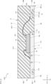
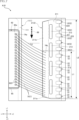
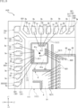
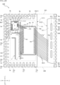
図1は、半導体装置A10を示す斜視図である。図2は、半導体装置A10を示す平面図である。図2においては、理解の便宜上、封止樹脂8を透過して、封止樹脂8の外形を想像線(二点鎖線)で示している。図3は、半導体装置A10を示す底面図である。図4は、図2のIV-IV線に沿う断面図である。図5は、図2のV-V線に沿う断面図である。図6は、図2のVI-VI線に沿う断面図である。図7は、図2の部分拡大図である。図8は、図2の部分拡大図である。図9は、リード1のダイパッド部11(後述)を示す平面図である。
FIG. 1 is a perspective view showing the semiconductor device A10. FIG. 2 is a plan view showing the semiconductor device A10. In FIG. 2, for convenience of understanding, the outline of the sealing resin 8 is shown by an imaginary line (two-dot chain line) that is transmitted through the sealing resin 8. FIG. 3 is a bottom view showing the semiconductor device A10. FIG. 4 is a cross-sectional view taken along line IV-IV in FIG. 2. FIG. 5 is a sectional view taken along line VV in FIG. 2. FIG. 6 is a cross-sectional view taken along line VI-VI in FIG. FIG. 7 is a partially enlarged view of FIG. 2. FIG. 8 is a partially enlarged view of FIG. 2. FIG. 9 is a plan view showing the die pad portion 11 (described later) of the lead 1. As shown in FIG.
半導体装置A10は、厚さ方向視(平面視)の形状が矩形状である。説明の便宜上、半導体装置A10の厚さ方向(平面視方向)を厚さ方向zとし、厚さ方向zに直交する半導体装置A10の一方の辺に沿う方向(図2および図3における左右方向)を第1方向x、厚さ方向zおよび第1方向xに直交する方向(図2および図3における上下方向)を第2方向yとする。また、厚さ方向zの一方側(図4~図6における上側)を第1側z1とし、他方側(図4~図6における下側)を第2側z2とする。第1方向xの一方側(図1および図2における左側)を第1側x1とし、他方側(図1および図2における右側)を第2側x2とする。第2方向yの一方側(図2における上側)を第1側y1とし、他方側(図2における下側)を第2側y2とする。なお、半導体装置A10の形状および各寸法は限定されない。
The semiconductor device A10 has a rectangular shape when viewed in the thickness direction (planar view). For convenience of explanation, the thickness direction (planar view direction) of the semiconductor device A10 is defined as the thickness direction z, and the direction along one side of the semiconductor device A10 perpendicular to the thickness direction z (left-right direction in FIGS. 2 and 3). is the first direction x, and the thickness direction z and the direction perpendicular to the first direction x (vertical direction in FIGS. 2 and 3) is the second direction y. Further, one side in the thickness direction z (upper side in FIGS. 4 to 6) is referred to as a first side z1, and the other side (lower side in FIGS. 4 to 6) is referred to as a second side z2. One side (the left side in FIGS. 1 and 2) in the first direction x is defined as a first side x1, and the other side (the right side in FIGS. 1 and 2) is defined as a second side x2. One side (upper side in FIG. 2) of the second direction y is defined as a first side y1, and the other side (lower side in FIG. 2) is defined as a second side y2. Note that the shape and dimensions of the semiconductor device A10 are not limited.
リード1、リード2、および複数のリード3(以下では、まとめて示す場合に、「リード1~3」と記載する場合がある)は、半導体素子61,62と、半導体装置A10が搭載される配線基板との導通経路を構成する部材である。なお、複数のリード3の一部には、半導体素子61,62に導通しないものも含まれている。リード1~3は、たとえば、金属板にエッチング処理または打ち抜き加工等を施すことにより形成されている。リード1~3は、金属からなり、好ましくはCuおよびNiのいずれか、またはこれらの合金や42アロイなどからなる。本実施形態においては、リード1~3が、Cuからなる場合を例に説明する。リード1~3の厚さは、たとえば0.08~0.3mmであり、本実施形態においては0.2mm程度である。
Lead 1, lead 2, and a plurality of leads 3 (hereinafter, when shown collectively, may be referred to as "leads 1 to 3") are mounted with semiconductor elements 61 and 62 and semiconductor device A10. This is a member that forms a conduction path with the wiring board. Note that some of the plurality of leads 3 include those that are not electrically connected to the semiconductor elements 61 and 62. The leads 1 to 3 are formed, for example, by etching or punching a metal plate. Leads 1 to 3 are made of metal, preferably Cu or Ni, or an alloy thereof, 42 alloy, or the like. In this embodiment, the case where leads 1 to 3 are made of Cu will be explained as an example. The thickness of the leads 1 to 3 is, for example, 0.08 to 0.3 mm, and in this embodiment is about 0.2 mm.
図2に示すように、リード1は、半導体装置A10の第1方向xの第1側x1寄りに配置され、第2方向yの全体に広がっている。リード2は、リード1から離間し、半導体装置A10の第1方向xの第2側x2寄りに配置されている。各リード3は、リード1およびリード2から離間し、また、互いに離間して、半導体装置A10の第1方向xの両端部または第2方向yの両端部のいずれかに配置されている。厚さ方向zに視た寸法は、リード1がリード2より大きく、各リード3がリード2より大きい。
As shown in FIG. 2, the lead 1 is arranged closer to the first side x1 in the first direction x of the semiconductor device A10, and extends throughout the second direction y. The lead 2 is spaced apart from the lead 1 and is placed closer to the second side x2 in the first direction x of the semiconductor device A10. Each lead 3 is spaced apart from the lead 1 and the lead 2, and spaced apart from each other, and is arranged at either both ends in the first direction x or both ends in the second direction y of the semiconductor device A10. In terms of dimensions in the thickness direction z, lead 1 is larger than lead 2, and each lead 3 is larger than lead 2.
リード1は、半導体素子61,62を支持し、ダイパッド部11および複数の端子部12を備えている。
The lead 1 supports the semiconductor elements 61 and 62 and includes a die pad portion 11 and a plurality of terminal portions 12.
ダイパッド部11は、半導体素子61および半導体素子62が搭載される。ダイパッド部11は、半導体装置A10の第1方向xの第1側x1寄りで、第2方向yの中央に位置し、厚さ方向zに視て略矩形状である。ダイパッド部11は、主面111、裏面112、および裏面側凹部113を備えている。主面111および裏面112は、厚さ方向zにおいて互いに反対側を向いている。主面111は、厚さ方向zの第1側z1を向いている。主面111は、半導体素子61,62が搭載される面である。主面111は、図9に示すように、端縁111aを備えている。端縁111aは、主面111の第1方向xの第1側x1で第2方向yに延びる端縁である。裏面112は、厚さ方向zの第2側z2を向いている。裏面112は、封止樹脂8から露出して、裏面端子になる。
A semiconductor element 61 and a semiconductor element 62 are mounted on the die pad section 11. The die pad portion 11 is located near the first side x1 in the first direction x of the semiconductor device A10, at the center in the second direction y, and has a substantially rectangular shape when viewed in the thickness direction z. The die pad portion 11 includes a main surface 111 , a back surface 112 , and a back-side recess 113 . The main surface 111 and the back surface 112 face opposite sides in the thickness direction z. The main surface 111 faces the first side z1 in the thickness direction z. The main surface 111 is a surface on which the semiconductor elements 61 and 62 are mounted. The main surface 111 has an edge 111a, as shown in FIG. The edge 111a is an edge extending in the second direction y on the first side x1 of the main surface 111 in the first direction x. The back surface 112 faces the second side z2 in the thickness direction z. The back surface 112 is exposed from the sealing resin 8 and becomes a back terminal.
裏面側凹部113は、ダイパッド部11の一部が裏面112から厚さ方向zの第1側z1に凹んだ部分である。ダイパッド部11のうち裏面側凹部113が位置する部分の厚さ(厚さ方向zの寸法)は、裏面112が位置する部分の厚さの半分程度である。裏面側凹部113は、たとえば厚さ方向zの第2側z2からのハーフエッチング処理により形成される。図3に示すように、裏面側凹部113は、裏面112の周囲に配置されている。裏面側凹部113は、封止樹脂8から露出せず、封止樹脂8によって覆われている。これにより、リード1が封止樹脂8から厚さ方向zの第2側z2に剥離することが抑制される。なお、ダイパッド部11の形状は限定されない。たとえば、ダイパッド部11は、裏面側凹部113を備えなくてもよい。
The back side recess 113 is a part where a part of the die pad part 11 is recessed from the back surface 112 toward the first side z1 in the thickness direction z. The thickness of the portion of the die pad portion 11 where the back side recess 113 is located (dimension in the thickness direction z) is approximately half the thickness of the portion where the back surface 112 is located. The back side recess 113 is formed, for example, by half-etching from the second side z2 in the thickness direction z. As shown in FIG. 3, the back surface side recess 113 is arranged around the back surface 112. The back side recess 113 is not exposed from the sealing resin 8 and is covered with the sealing resin 8. This prevents the lead 1 from peeling off from the sealing resin 8 toward the second side z2 in the thickness direction z. Note that the shape of the die pad portion 11 is not limited. For example, the die pad portion 11 does not need to include the back side recess 113.
ダイパッド部11は、開口部4を備えている。なお、図2、図8、および図9においては、理解の便宜上、開口部4に比較的細かいハッチングを付している。開口部4は、主面111に開口端を有する開口部であり、本実施形態では、主面111から厚さ方向zの第2側z2に凹んだ凹部である。開口部4の深さ(厚さ方向zの寸法)は、ダイパッド部11の厚さ(厚さ方向zにおける主面111と裏面112との距離)の半分程度である。開口部4は、たとえば厚さ方向zの第1側z1からのハーフエッチング処理により形成される。開口部4は、図9に示すように、開口部41~45を含んでいる。
The die pad section 11 includes an opening 4. In addition, in FIG. 2, FIG. 8, and FIG. 9, for convenience of understanding, the opening 4 is provided with relatively fine hatching. The opening 4 is an opening having an open end on the main surface 111, and in this embodiment, is a recess recessed from the main surface 111 toward the second side z2 in the thickness direction z. The depth of the opening 4 (dimension in the thickness direction z) is approximately half the thickness of the die pad portion 11 (the distance between the main surface 111 and the back surface 112 in the thickness direction z). The opening 4 is formed, for example, by half etching from the first side z1 in the thickness direction z. The opening 4 includes openings 41 to 45, as shown in FIG.
開口部41は、第1方向xにおいて、図9において想像線(二点鎖線)で示す半導体素子62と端縁111aとの間に位置し、第2方向yに延びている。本実施形態では、厚さ方向zに視て、開口部41の第2方向yにおける両端は、主面111の外縁より内側に位置する。開口部42は、開口部41の第2方向yの第1側y1の端部につながり、第1方向xの第1側x1に延びている。つまり、開口部42は、開口部41の第1方向xの第1側x1に位置する。本実施形態では、厚さ方向zに視て、開口部42の第1方向xにおける両端は、主面111の外縁より内側に位置する。図9において想像線(二点鎖線)で示す半導体素子61は、第2方向yにおいて、開口部42の第1側y1に配置されている。開口部4のうち、開口部41および開口部42で構成される部分は、厚さ方向zに視てL字形状である。
The opening 41 is located in the first direction x between the semiconductor element 62 and the edge 111a shown by an imaginary line (two-dot chain line) in FIG. 9, and extends in the second direction y. In this embodiment, both ends of the opening 41 in the second direction y are located inside the outer edge of the main surface 111 when viewed in the thickness direction z. The opening 42 is connected to the end of the first side y1 in the second direction y of the opening 41 and extends to the first side x1 in the first direction x. That is, the opening 42 is located on the first side x1 of the opening 41 in the first direction x. In this embodiment, both ends of the opening 42 in the first direction x are located inside the outer edge of the main surface 111 when viewed in the thickness direction z. The semiconductor element 61 shown by an imaginary line (two-dot chain line) in FIG. 9 is arranged on the first side y1 of the opening 42 in the second direction y. A portion of the opening 4 that is constituted by the opening 41 and the opening 42 is L-shaped when viewed in the thickness direction z.
開口部43は、第1方向xにおいて、半導体素子62と開口部41との間に位置し、第2方向yに延びている。本実施形態では、厚さ方向zに視て、開口部43の第2方向yにおける両端は、主面111の外縁より内側に位置する。開口部44は、開口部43の第2方向yの第1側y1の端部につながり、第1方向xの第1側x1に延びている。つまり、開口部44は、開口部43の第1方向xの第1側x1に位置する。また、開口部44は、第2方向yにおいて、半導体素子61と開口部42との間に位置する。本実施形態では、厚さ方向zに視て、開口部44の第1方向xにおける両端は、主面111の外縁より内側に位置する。開口部45は、開口部43の第2方向yの第1側y1の端部につながり、第2方向yの第1側y1に延びている。つまり、開口部45は、開口部43の第2方向yの第1側y1に位置する。本実施形態では、厚さ方向zに視て、開口部45の第2方向yにおける両端は、主面111の外縁より内側に位置する。開口部4のうち、開口部43、開口部44、および開口部45で構成される部分は、厚さ方向zに視てT字形状である。
The opening 43 is located between the semiconductor element 62 and the opening 41 in the first direction x, and extends in the second direction y. In this embodiment, both ends of the opening 43 in the second direction y are located inside the outer edge of the main surface 111 when viewed in the thickness direction z. The opening 44 is connected to the end of the first side y1 in the second direction y of the opening 43 and extends to the first side x1 in the first direction x. That is, the opening 44 is located on the first side x1 of the opening 43 in the first direction x. Furthermore, the opening 44 is located between the semiconductor element 61 and the opening 42 in the second direction y. In this embodiment, both ends of the opening 44 in the first direction x are located inside the outer edge of the main surface 111 when viewed in the thickness direction z. The opening 45 is connected to the end of the first side y1 in the second direction y of the opening 43 and extends to the first side y1 in the second direction y. That is, the opening 45 is located on the first side y1 of the opening 43 in the second direction y. In this embodiment, both ends of the opening 45 in the second direction y are located inside the outer edge of the main surface 111 when viewed in the thickness direction z. A portion of the opening 4 that is constituted by the opening 43, the opening 44, and the opening 45 is T-shaped when viewed in the thickness direction z.
ダイパッド部11の主面111は、図9に示すように、第1領域51、第2領域52、および第3領域53を含んでいる。図9において、第1領域51、第2領域52、および第3領域53は、想像線(二点鎖線)で示されており、比較的粗いハッチングが付されている。第1領域51は、開口部41および開口部42と、開口部43および開口部44とによってはさまれた領域である。第1領域51は、半導体素子62の第1方向xの第1側x1に位置し、図2に示すように、ワイヤ7(後述するワイヤ73)が接合される領域である。第1領域51には、めっき処理が施されていてもよい。当該めっき処理により形成されるめっき層は、たとえばAgを含む金属からなる。当該めっき層は、ワイヤ73の接合強度を高めつつ、ワイヤ73のワイヤボンディング時の衝撃からリード1を保護する。第2領域52は、開口部43および開口部45の第1方向xの第2側x2の領域である。第2領域52は、図2に示すように、半導体素子62が搭載される領域である。第3領域53は、開口部45の第1方向xの第1側x1であり、かつ、開口部44の第2方向yの第1側y1の領域である。第3領域53は、ダイパッド部11の主面111の第1方向xにおける中心より第1側x1に位置し、第2方向yにおける中心より第1側y1に位置する。第3領域53は、図2に示すように、半導体素子61が搭載される領域である。
The main surface 111 of the die pad section 11 includes a first region 51, a second region 52, and a third region 53, as shown in FIG. In FIG. 9, the first region 51, the second region 52, and the third region 53 are shown by imaginary lines (two-dot chain lines), and are relatively roughly hatched. The first region 51 is a region sandwiched between the openings 41 and 42 and the openings 43 and 44. The first region 51 is located on the first side x1 of the semiconductor element 62 in the first direction x, and is a region to which the wire 7 (wire 73 described later) is bonded, as shown in FIG. The first region 51 may be subjected to plating treatment. The plating layer formed by the plating process is made of a metal containing Ag, for example. The plating layer protects the lead 1 from impact during wire bonding of the wire 73 while increasing the bonding strength of the wire 73. The second region 52 is a region on the second side x2 of the openings 43 and 45 in the first direction x. The second region 52 is a region where a semiconductor element 62 is mounted, as shown in FIG. The third region 53 is a region on the first side x1 of the opening 45 in the first direction x, and is a region on the first side y1 of the opening 44 in the second direction y. The third region 53 is located on the first side x1 from the center of the main surface 111 of the die pad portion 11 in the first direction x, and is located on the first side y1 from the center in the second direction y. The third area 53 is an area where the semiconductor element 61 is mounted, as shown in FIG.
逆に言うと、第1領域51、第2領域52、および第3領域53は、開口部4によって区画された領域である。開口部43は、第1領域51と第2領域52とを区画している。開口部44は、第1領域51と第3領域53とを区画している。開口部45は、第2領域52と第3領域53とを区画している。なお、開口部4の形状および配置は上述したものに限定されず、第1領域51、第2領域52、および第3領域53の形状および配置は上述したものに限定されない。
In other words, the first region 51, the second region 52, and the third region 53 are regions partitioned by the opening 4. The opening 43 partitions a first region 51 and a second region 52. The opening 44 partitions the first region 51 and the third region 53. The opening 45 partitions a second region 52 and a third region 53. Note that the shape and arrangement of the opening 4 are not limited to those described above, and the shapes and arrangement of the first region 51, second region 52, and third region 53 are not limited to those described above.
複数の端子部12は、半導体装置A10を配線基板に実装する際に、配線基板に接合される。各端子部12は、ダイパッド部11につながっており、厚さ方向zに視て略矩形状である。複数の端子部12は、6個の端子部12a、2個の端子部12b、8個の端子部12c、および端子部12d,12eを含んでいる。6個の端子部12aは、ダイパッド部11の第1方向xの第1側x1につながり、第2方向yの第2側y2寄りで第2方向yに沿って配列されている。当該6個の端子部12aは、第1方向xに視て開口部4(開口部41)に重なっている。2個の端子部12bは、ダイパッド部11の第2方向yの第1側y1につながり、第1方向xの第2側x2寄りで第2方向yに沿って配列されている。8個の端子部12cは、ダイパッド部11の第2方向yの第2側y2につながり、第1方向xに沿って配列されている。端子部12dは、ダイパッド部11の第1方向xの第1側x1で第2方向yの第1側y1の角につながっている。端子部12eは、ダイパッド部11の第1方向xの第1側x1で第2方向yの第2側y2の角につながっている。
The plurality of terminal portions 12 are bonded to the wiring board when the semiconductor device A10 is mounted on the wiring board. Each terminal portion 12 is connected to the die pad portion 11 and has a substantially rectangular shape when viewed in the thickness direction z. The plurality of terminal sections 12 include six terminal sections 12a, two terminal sections 12b, eight terminal sections 12c, and terminal sections 12d and 12e. The six terminal parts 12a are connected to the first side x1 of the die pad part 11 in the first direction x, and are arranged along the second direction y near the second side y2 in the second direction y. The six terminal portions 12a overlap the opening 4 (opening 41) when viewed in the first direction x. The two terminal portions 12b are connected to the first side y1 of the die pad portion 11 in the second direction y, and are arranged along the second direction y near the second side x2 in the first direction x. The eight terminal portions 12c are connected to the second side y2 of the die pad portion 11 in the second direction y, and are arranged along the first direction x. The terminal portion 12d is connected to a corner of the first side y1 in the second direction y at the first side x1 in the first direction x of the die pad portion 11. The terminal portion 12e is connected to a corner of the die pad portion 11 on the first side x1 in the first direction x and on the second side y2 in the second direction y.
各端子部12は、主面121、裏面122、および端面123を備えている。主面121および裏面122は、厚さ方向zにおいて互いに反対側を向いている。主面121は、厚さ方向zの第1側z1を向いている。主面121とダイパッド部11の主面111とは、面一になっている。裏面122は、厚さ方向zの第2側z2を向いている。裏面122とダイパッド部11の裏面112とは、図3に示すように離間しており、厚さ方向zでの位置が互いに同じ(あるいは略同じ)である。端面123は、主面121および裏面122に直交し、主面121および裏面122につながる面である。端子部12dおよび端子部12eはそれぞれ、2個の端面123を備えている。端面123は、製造工程における切断工程でのシンギュレーションにより形成される。端面123および裏面122は、封止樹脂8から露出してつながっており、端子になる(図5参照)。なお、端子部12の形状、配置位置および個数は限定されない。
Each terminal portion 12 includes a main surface 121, a back surface 122, and an end surface 123. The main surface 121 and the back surface 122 face opposite to each other in the thickness direction z. The main surface 121 faces the first side z1 in the thickness direction z. The main surface 121 and the main surface 111 of the die pad portion 11 are flush with each other. The back surface 122 faces the second side z2 in the thickness direction z. The back surface 122 and the back surface 112 of the die pad portion 11 are spaced apart from each other as shown in FIG. 3, and are at the same (or substantially the same) position in the thickness direction z. The end surface 123 is a surface that is perpendicular to the main surface 121 and the back surface 122 and connected to the main surface 121 and the back surface 122. The terminal portion 12d and the terminal portion 12e each include two end surfaces 123. The end surface 123 is formed by singulation in the cutting process in the manufacturing process. The end surface 123 and the back surface 122 are exposed from the sealing resin 8 and connected, and become a terminal (see FIG. 5). Note that the shape, arrangement position, and number of terminal portions 12 are not limited.
リード2は、リード1から第1方向xの第2側x2に離間して配置されている。リード1のダイパッド部11とリード2とは、第1方向xに並んで配置されている。リード2は、複数のワイヤ7(後述する複数のワイヤ74)によって、半導体素子62に導通接続している。リード2は、パッド部21および複数の端子部22を備えている。
The lead 2 is spaced apart from the lead 1 on the second side x2 in the first direction x. The die pad portion 11 of the lead 1 and the lead 2 are arranged side by side in the first direction x. The lead 2 is electrically connected to the semiconductor element 62 by a plurality of wires 7 (a plurality of wires 74 to be described later). The lead 2 includes a pad portion 21 and a plurality of terminal portions 22 .
パッド部21は、複数のワイヤ74が接合される。パッド部21は、主面211、裏面212、および貫通孔213を備えている。主面211および裏面212は、厚さ方向zにおいて互いに反対側を向いている。主面211は、厚さ方向zの第1側z1を向いている。主面211は、複数のワイヤ74が接合される面である。主面211は、図7に示すように、接合領域211aおよび非接合領域211bを含んでいる。図7において、接合領域211aおよび非接合領域211bは、想像線(二点鎖線)で示されている。接合領域211aは、複数のワイヤ74が接合される領域であり、主面211において、第2方向yの第2側y2寄りに配置されている。非接合領域211bは、複数のワイヤ74が接合されない領域であり、第2方向yにおいて、接合領域211aに対して第1側y1に配置されている。第2方向yにおける接合領域211aの寸法L1は、第2方向yにおけるリード2の寸法L2の40%以上60%以下である。接合領域211aには、めっき処理が施されていてもよい。当該めっき処理により形成されるめっき層は、たとえばAgを含む金属からなる。当該めっき層は、ワイヤ74の接合強度を高めつつ、ワイヤ74のワイヤボンディング時の衝撃からリード2を保護する。裏面212は、厚さ方向zの第2側z2を向いている。裏面212は、封止樹脂8に覆われている。パッド部21の厚さ(厚さ方向zの寸法)は、ダイパッド部11の厚さの半分程度であり、ダイパッド部11のうち裏面側凹部113が位置する部分の厚さと同程度である。パッド部21は、たとえば厚さ方向zの第2側z2からのハーフエッチング処理により形成される。
A plurality of wires 74 are bonded to the pad portion 21. The pad portion 21 includes a main surface 211, a back surface 212, and a through hole 213. The main surface 211 and the back surface 212 face opposite to each other in the thickness direction z. The main surface 211 faces the first side z1 in the thickness direction z. The main surface 211 is a surface to which the plurality of wires 74 are bonded. As shown in FIG. 7, the main surface 211 includes a bonding region 211a and a non-bonding region 211b. In FIG. 7, the bonded region 211a and the non-bonded region 211b are indicated by imaginary lines (two-dot chain lines). The bonding region 211a is a region where the plurality of wires 74 are bonded, and is disposed on the main surface 211 closer to the second side y2 in the second direction y. The non-bonded region 211b is a region where the plurality of wires 74 are not bonded, and is arranged on the first side y1 with respect to the bonded region 211a in the second direction y. The dimension L1 of the bonding region 211a in the second direction y is 40% or more and 60% or less of the dimension L2 of the lead 2 in the second direction y. The bonding region 211a may be subjected to plating treatment. The plating layer formed by the plating process is made of a metal containing Ag, for example. The plating layer protects the leads 2 from impact during wire bonding of the wires 74 while increasing the bonding strength of the wires 74. The back surface 212 faces the second side z2 in the thickness direction z. The back surface 212 is covered with the sealing resin 8. The thickness of the pad portion 21 (dimension in the thickness direction z) is approximately half the thickness of the die pad portion 11, and is approximately the same as the thickness of the portion of the die pad portion 11 where the backside recess 113 is located. The pad portion 21 is formed, for example, by half-etching from the second side z2 in the thickness direction z.
貫通孔213は、パッド部21を厚さ方向zに貫通する孔である。貫通孔213は、半導体装置A10の製造工程の封止樹脂8の形成工程において、封止樹脂8の材料がパッド部21の裏面212側に充填されやすくする。本実施形態では、パッド部21は、第2方向yに長い略矩形状の貫通孔213が第2方向yに4個配列されている。なお、貫通孔213の形状、数、および配置は限定されない。また、パッド部21は貫通孔213を備えなくてもよい。
The through hole 213 is a hole that penetrates the pad portion 21 in the thickness direction z. The through hole 213 facilitates filling the back surface 212 side of the pad portion 21 with the material of the sealing resin 8 in the process of forming the sealing resin 8 in the manufacturing process of the semiconductor device A10. In this embodiment, the pad portion 21 has four substantially rectangular through holes 213 that are long in the second direction y and are arranged in the second direction y. Note that the shape, number, and arrangement of the through holes 213 are not limited. Further, the pad portion 21 does not need to include the through hole 213.
複数の端子部22は、半導体装置A10を配線基板に実装する際に、配線基板に接合される。各端子部22は、パッド部21の第1方向xの第2側x2につながっており、厚さ方向zに視て略矩形状である。本実施形態では、12個の端子部22が、第2方向yに沿って等間隔で配列されている。
The plurality of terminal parts 22 are bonded to the wiring board when the semiconductor device A10 is mounted on the wiring board. Each terminal portion 22 is connected to the second side x2 of the pad portion 21 in the first direction x, and has a substantially rectangular shape when viewed in the thickness direction z. In this embodiment, twelve terminal parts 22 are arranged at equal intervals along the second direction y.
各端子部22は、主面221、裏面222、および端面223を備えている。主面221および裏面222は、厚さ方向zにおいて互いに反対側を向いている。主面221は、厚さ方向zの第1側z1を向いている。主面221とパッド部21の主面211とは、面一になっている。裏面222は、厚さ方向zの第2側z2を向いている。本実施形態では、図3に示すように、リード2の端子部22の裏面222と、ダイパッド部11の裏面112との距離L3は十分大きく、たとえば半導体装置A10の第1方向xの寸法L4の30%以上40%以下である。なお、裏面222と裏面112との距離は、これに限定されない。端面223は、主面221および裏面222に直交し、主面221および裏面222につながる面である。端面223は、製造工程における切断工程でのシンギュレーションにより形成される。端面223および裏面222は、封止樹脂8から露出してつながっており、端子になる(図4および図5参照)。なお、端子部22の形状、配置位置および個数は限定されない。
Each terminal portion 22 includes a main surface 221, a back surface 222, and an end surface 223. The main surface 221 and the back surface 222 face opposite to each other in the thickness direction z. The main surface 221 faces the first side z1 in the thickness direction z. The main surface 221 and the main surface 211 of the pad portion 21 are flush with each other. The back surface 222 faces the second side z2 in the thickness direction z. In this embodiment, as shown in FIG. 3, the distance L3 between the back surface 222 of the terminal section 22 of the lead 2 and the back surface 112 of the die pad section 11 is sufficiently large, and for example, the distance L3 in the first direction x of the semiconductor device A10 is It is 30% or more and 40% or less. Note that the distance between the back surface 222 and the back surface 112 is not limited to this. The end surface 223 is a surface that is perpendicular to the main surface 221 and the back surface 222 and connected to the main surface 221 and the back surface 222. The end surface 223 is formed by singulation in the cutting process in the manufacturing process. The end surface 223 and the back surface 222 are exposed from the sealing resin 8 and connected, and become terminals (see FIGS. 4 and 5). Note that the shape, arrangement position, and number of the terminal portions 22 are not limited.
複数のリード3は、半導体素子61,62と、半導体装置A10が搭載される配線基板との導通経路を構成する。なお、複数のリード3には、半導体素子61,62に導通しないいわゆるダミーリードも含まれている。各リード3は、パッド部31および端子部32を備えている。
The plurality of leads 3 constitute a conduction path between the semiconductor elements 61 and 62 and the wiring board on which the semiconductor device A10 is mounted. Note that the plurality of leads 3 also include so-called dummy leads that are not electrically connected to the semiconductor elements 61 and 62. Each lead 3 includes a pad portion 31 and a terminal portion 32.
パッド部31は、ワイヤ7(後述するワイヤ71)が接合されるための部位である。なお、パッド部31は、ワイヤ71が接合されている場合と接合されていない場合がある。パッド部31は、主面311および裏面312を備えている。主面311および裏面312は、厚さ方向zにおいて互いに反対側を向いている。主面311は、厚さ方向zの第1側z1を向いている。主面311は、ワイヤ71が接合される面である。主面311には、めっき処理が施されていてもよい。当該めっき処理により形成されるめっき層は、たとえばAgを含む金属からなる。当該めっき層は、ワイヤ71の接合強度を高めつつ、ワイヤ71のワイヤボンディング時の衝撃からリード3を保護する。なお、ワイヤ71が接合されるリード3にのみめっき層が形成されてもよい。裏面312は、厚さ方向zの第2側z2を向いている。裏面312は、封止樹脂8に覆われている。パッド部31の厚さ(厚さ方向zの寸法)は、ダイパッド部11の厚さの半分程度であり、ダイパッド部11のうち裏面側凹部113が位置する部分の厚さと同程度である。パッド部31は、たとえば厚さ方向zの第2側z2からのハーフエッチング処理により形成される。
The pad portion 31 is a portion to which the wire 7 (wire 71 to be described later) is bonded. Note that the pad portion 31 may or may not be joined to the wire 71. The pad portion 31 includes a main surface 311 and a back surface 312. The main surface 311 and the back surface 312 face opposite to each other in the thickness direction z. The main surface 311 faces the first side z1 in the thickness direction z. The main surface 311 is a surface to which the wire 71 is bonded. The main surface 311 may be subjected to plating treatment. The plating layer formed by the plating process is made of a metal containing Ag, for example. The plating layer protects the leads 3 from impact during wire bonding of the wires 71 while increasing the bonding strength of the wires 71. Note that the plating layer may be formed only on the lead 3 to which the wire 71 is bonded. The back surface 312 faces the second side z2 in the thickness direction z. The back surface 312 is covered with sealing resin 8. The thickness of the pad portion 31 (dimension in the thickness direction z) is approximately half the thickness of the die pad portion 11, and is approximately the same as the thickness of the portion of the die pad portion 11 where the backside recess 113 is located. The pad portion 31 is formed, for example, by half-etching from the second side z2 in the thickness direction z.
端子部32は、半導体装置A10を配線基板に実装する際に、配線基板に接合される。端子部32は、パッド部31につながっており、厚さ方向zに視て略矩形状である。端子部32は、主面321、裏面322、および端面323を備えている。主面321および裏面322は、厚さ方向zにおいて互いに反対側を向いている。主面321は、厚さ方向zの第1側z1を向いている。主面321とパッド部31の主面311とは、面一になっている。ワイヤ71は、端子部32の主面321に接合されてもよい。裏面322は、厚さ方向zの第2側z2を向いている。端面323は、主面321および裏面322に直交し、主面321および裏面322につながる面である。端面323は、製造工程における切断工程でのシンギュレーションにより形成される。端面323および裏面322は、封止樹脂8から露出してつながっており、端子になる(図4参照)。なお、端子部32の形状は限定されない。
The terminal portion 32 is bonded to the wiring board when the semiconductor device A10 is mounted on the wiring board. The terminal portion 32 is connected to the pad portion 31 and has a substantially rectangular shape when viewed in the thickness direction z. The terminal portion 32 includes a main surface 321, a back surface 322, and an end surface 323. The main surface 321 and the back surface 322 face opposite to each other in the thickness direction z. The main surface 321 faces the first side z1 in the thickness direction z. The main surface 321 and the main surface 311 of the pad portion 31 are flush with each other. The wire 71 may be joined to the main surface 321 of the terminal portion 32. The back surface 322 faces the second side z2 in the thickness direction z. The end surface 323 is a surface that is perpendicular to the main surface 321 and the back surface 322 and connected to the main surface 321 and the back surface 322. The end surface 323 is formed by singulation in the cutting process in the manufacturing process. The end surface 323 and the back surface 322 are exposed from the sealing resin 8 and connected, and become a terminal (see FIG. 4). Note that the shape of the terminal portion 32 is not limited.
複数のリード3は、図2に示すように、複数のリード3a、複数のリード3b、リード3c、リード3e、一対のリード3f、および一対のリード3gを含んでいる。
As shown in FIG. 2, the plurality of leads 3 include a plurality of leads 3a, a plurality of leads 3b, a lead 3c, a lead 3e, a pair of leads 3f, and a pair of leads 3g.
本実施形態では、複数のリード3は、7個のリード3aを含んでいる。なお、リード3aの数は限定されない。複数のリード3aは、半導体装置A10の第1方向xの第1側x1の端部の第2方向yの第1側y1寄りに配置されている。複数のリード3aは、ダイパッド部11の第1方向xの第1側x1に、第2方向yにおいて端子部12aと端子部12dとの間で第2方向yに沿って配列されている。また、本実施形態では、複数のリード3は、7個のリード3bを含んでいる。なお、リード3bの数は限定されない。複数のリード3bは、半導体装置A10の第2方向yの第1側y1の端部の第1方向xの第1側x1寄りに配置されている。複数のリード3bは、ダイパッド部11の第2方向yの第1側y1に、第1方向xにおいて端子部12bと端子部12dとの間で第1方向xに沿って配列されている。複数のリード3aおよび複数のリード3bは、ワイヤ71を介して半導体素子61に導通できるように配置されている。本実施形態では、複数のリード3aおよび複数のリード3bのほとんどは半導体素子61に導通しているが、半導体素子61に導通していないものも含まれている。なお、複数のリード3aおよび複数のリード3bのいずれが半導体素子61に導通するか、また、半導体素子61のどの電極611(後述)に導通接続されているかは限定されない。図8に示すように、複数のリード3aおよび複数のリード3bの各パッド部31はいずれも、厚さ方向zに視て、半導体素子61の中心である素子中心61cに向けて延びている。
In this embodiment, the plurality of leads 3 include seven leads 3a. Note that the number of leads 3a is not limited. The plurality of leads 3a are arranged near the first side y1 in the second direction y at the end of the first side x1 in the first direction x of the semiconductor device A10. The plurality of leads 3a are arranged on the first side x1 of the die pad portion 11 in the first direction x, and along the second direction y between the terminal portions 12a and 12d in the second direction y. Further, in this embodiment, the plurality of leads 3 includes seven leads 3b. Note that the number of leads 3b is not limited. The plurality of leads 3b are arranged near the first side x1 in the first direction x at the end of the first side y1 in the second direction y of the semiconductor device A10. The plurality of leads 3b are arranged along the first direction x on the first side y1 of the die pad portion 11 in the second direction y between the terminal portions 12b and 12d. The plurality of leads 3a and the plurality of leads 3b are arranged so as to be electrically connected to the semiconductor element 61 via the wire 71. In this embodiment, most of the plurality of leads 3a and the plurality of leads 3b are electrically connected to the semiconductor element 61, but some are not electrically connected to the semiconductor element 61. Note that which of the plurality of leads 3a and the plurality of leads 3b is electrically connected to the semiconductor element 61, and which electrode 611 (described later) of the semiconductor element 61 is electrically connected is not limited. As shown in FIG. 8, each pad portion 31 of the plurality of leads 3a and the plurality of leads 3b extends toward the element center 61c, which is the center of the semiconductor element 61, when viewed in the thickness direction z.
また、本実施形態では、複数のリード3は、1個のリード3cおよび1個のリード3eを含んでいる。なお、リード3cおよびリード3eの数は限定されない。リード3cは、ダイパッド部11の第1方向xの第1側x1に、第2方向yにおいて端子部12aと端子部12eとの間に配置されている。リード3eは、ダイパッド部11の第2方向yの第2側y2に、第1方向xにおいて端子部12cと端子部12eとの間に配置されている。リード3cおよびリード3eは、いわゆるダミーリードである。
Furthermore, in this embodiment, the plurality of leads 3 include one lead 3c and one lead 3e. Note that the number of leads 3c and leads 3e is not limited. The lead 3c is arranged on the first side x1 of the die pad section 11 in the first direction x, between the terminal section 12a and the terminal section 12e in the second direction y. The lead 3e is arranged on the second side y2 of the die pad section 11 in the second direction y, between the terminal section 12c and the terminal section 12e in the first direction x. Leads 3c and 3e are so-called dummy leads.
また、本実施形態では、複数のリード3は、一対のリード3fおよび一対のリード3gを含んでいる。一対のリード3gは、リード2の第2方向yの第1側y1および第2側y2にそれぞれ1個ずつ配置されている。一方のリード3gは半導体装置A10の第1方向xの第2側x2で第2方向yの第1側y1の角に配置され、他方のリード3gは半導体装置A10の第1方向xの第2側x2で第2方向yの第2側y2の角に配置されている。なお、複数のリード3は、リード3gを含んでいなくてもよい。一対のリード3fは、リード2の第2方向yの第1側y1および第2側y2にそれぞれ1個ずつ配置されている。各リード3fは、第2方向yにおいてリード2と各リード3gとの間にそれぞれ配置されている。なお、リード3fの数は限定されない。リード3fおよびリード3gは、いわゆるダミーリードである。
Furthermore, in this embodiment, the plurality of leads 3 include a pair of leads 3f and a pair of leads 3g. The pair of leads 3g are arranged one each on the first side y1 and the second side y2 of the lead 2 in the second direction y. One lead 3g is arranged at a corner of the first side y1 in the second direction y on the second side x2 in the first direction x of the semiconductor device A10, and the other lead 3g is arranged on the second side x2 in the first direction It is arranged at the corner of the second side y2 in the second direction y on the side x2. Note that the plurality of leads 3 may not include the lead 3g. The pair of leads 3f is arranged one each on the first side y1 and the second side y2 of the lead 2 in the second direction y. Each lead 3f is arranged between the lead 2 and each lead 3g in the second direction y. Note that the number of leads 3f is not limited. Lead 3f and lead 3g are so-called dummy leads.
リード1~3のうち封止樹脂8から露出した面には、たとえばSnを含むめっき層が配置されてもよい。なお、めっき層の構成材料は限定されない。当該めっき層は、はんだ接合によって半導体装置A10を配線基板に表面実装させる際に、当該露出した面へのはんだの付着を良好なものにしつつ、はんだ接合に起因した当該露出した部分の浸食を防止する。なお、リード1~3の形状および配置は上記に限定されない。
A plating layer containing Sn, for example, may be disposed on the surfaces of the leads 1 to 3 exposed from the sealing resin 8. Note that the constituent material of the plating layer is not limited. When surface-mounting the semiconductor device A10 on a wiring board by soldering, the plating layer ensures good adhesion of solder to the exposed surface and prevents erosion of the exposed portion caused by soldering. do. Note that the shape and arrangement of the leads 1 to 3 are not limited to the above.
半導体素子61および半導体素子62は、半導体装置A10の電気的機能を発揮する要素である。半導体素子62は、スイッチング素子である。本実施形態では、半導体素子62は、窒化ガリウム(GaN)を用いたHEMT(High Electron Mobility Transistor:高電子移動度トランジスタ)である。なお、半導体素子62は、GaN以外の窒化物半導体が用いられてもよい。また、半導体素子62は、IGBT(Insulated Gate BipolarTransistor)、MOSFET(Metal Oxide Semiconductor Field Effect Transistor)、またはバイポーラトランジスタなどであってもよい。半導体素子62は、素子主面62a、素子裏面62b、複数の第1電極621、第2電極622、および複数の第3電極623を備えている。
The semiconductor element 61 and the semiconductor element 62 are elements that perform the electrical functions of the semiconductor device A10. The semiconductor element 62 is a switching element. In this embodiment, the semiconductor element 62 is a HEMT (High Electron Mobility Transistor) using gallium nitride (GaN). Note that the semiconductor element 62 may be made of a nitride semiconductor other than GaN. Furthermore, the semiconductor element 62 may be an IGBT (Insulated Gate Bipolar Transistor), a MOSFET (Metal Oxide Semiconductor Field Effect Transistor), a bipolar transistor, or the like. The semiconductor element 62 includes an element main surface 62a, an element back surface 62b, a plurality of first electrodes 621, a second electrode 622, and a plurality of third electrodes 623.
素子主面62aおよび素子裏面62bは、厚さ方向zにおいて互いに反対側を向いている。素子主面62aは厚さ方向zの第1側z1を向く面であり、素子裏面62bは厚さ方向zの第2側z2を向く面である。複数の第1電極621、第2電極622、および複数の第3電極623は、素子主面62aに配置されている。複数の第1電極621は、ソース電極であり、素子主面62aの第1方向xの第1側x1寄りに第2方向yに沿って並んで配列されている。第2電極622は、ゲート電極であり、素子主面62aの第2方向yの第1側y1寄りに配置されている。複数の第3電極623は、ドレイン電極であり、素子主面62aの第1方向xの第2側x2寄りに第2方向yに沿って並んで配列されている。なお、素子主面62aには、その他の電極も配置されている。また、各電極621~623の配置のレイアウトは限定されない。
The element main surface 62a and the element back surface 62b face opposite to each other in the thickness direction z. The element main surface 62a is a surface facing the first side z1 in the thickness direction z, and the element back surface 62b is a surface facing the second side z2 in the thickness direction z. A plurality of first electrodes 621, a plurality of second electrodes 622, and a plurality of third electrodes 623 are arranged on the element main surface 62a. The plurality of first electrodes 621 are source electrodes, and are arranged side by side along the second direction y closer to the first side x1 in the first direction x of the element main surface 62a. The second electrode 622 is a gate electrode, and is arranged near the first side y1 in the second direction y of the element main surface 62a. The plurality of third electrodes 623 are drain electrodes, and are arranged side by side along the second direction y closer to the second side x2 of the first direction x of the element main surface 62a. Note that other electrodes are also arranged on the element main surface 62a. Furthermore, the layout of the electrodes 621 to 623 is not limited.
半導体素子62は、図4~図6に示すように、接合部材65を介して、素子裏面62bがダイパッド部11の主面111に接合されている。本実施形態では、接合部材65は、たとえばAgペーストである。なお、接合部材65は、はんだまたは焼結銀接合材などの導電性接合材であってもよいし、絶縁性接合部材であってもよい。半導体素子62は、図2および図9に示すように、主面111の第2領域52、すなわち、開口部43および開口部44の第1方向xの第2側x2側に配置されている。
As shown in FIGS. 4 to 6, the back surface 62b of the semiconductor element 62 is bonded to the main surface 111 of the die pad portion 11 via a bonding member 65. In this embodiment, the bonding member 65 is, for example, Ag paste. Note that the bonding member 65 may be a conductive bonding material such as solder or a sintered silver bonding material, or may be an insulating bonding member. As shown in FIGS. 2 and 9, the semiconductor element 62 is disposed on the second region 52 of the main surface 111, that is, on the second side x2 of the openings 43 and 44 in the first direction x.
半導体素子61は、半導体素子62を駆動させる駆動素子である。半導体素子61は、外部から入力される制御信号に基づいて駆動信号を生成し、半導体素子62に出力する。また、半導体素子61は、半導体素子62から入力されるソースセンス信号などに基づいて、駆動信号の制御を行う。半導体素子61は、素子主面61a、素子裏面61b、および複数の電極611を備えている。
The semiconductor element 61 is a driving element that drives the semiconductor element 62. The semiconductor element 61 generates a drive signal based on a control signal input from the outside and outputs it to the semiconductor element 62. Further, the semiconductor element 61 controls the drive signal based on a source sense signal inputted from the semiconductor element 62 and the like. The semiconductor element 61 includes an element main surface 61a, an element back surface 61b, and a plurality of electrodes 611.
素子主面61aおよび素子裏面61bは、厚さ方向zにおいて互いに反対側を向いている。素子主面61aは厚さ方向zの第1側z1を向く面であり、素子裏面61bは厚さ方向zの第2側z2を向く面である。複数の電極611は、素子主面61aに配置されている。なお、各電極611の機能および配置は限定されない。
The element main surface 61a and the element back surface 61b face opposite sides in the thickness direction z. The element main surface 61a is a surface facing the first side z1 in the thickness direction z, and the element back surface 61b is a surface facing the second side z2 in the thickness direction z. The plurality of electrodes 611 are arranged on the element main surface 61a. Note that the function and arrangement of each electrode 611 are not limited.
半導体素子61は、図4に示すように、接合部材65を介して、素子裏面61bがダイパッド部11の主面111に接合されている。半導体素子61は、図2および図9に示すように、主面111の第3領域53、すなわち、開口部45の第1方向xの第1側x1であり、かつ、開口部44の第2方向yの第1側y1に配置されている。半導体素子61は、第1方向xにおいて半導体素子62に対して第1側x1で、第2方向yにおいて半導体素子62に対して第1側y1に配置されている。厚さ方向zに視た半導体素子61の中心である素子中心61cは、ダイパッド部11の主面111の第2方向yにおける中心より第1側y1に位置し、かつ、主面111の第1方向xにおける中心より第1側x1に位置している。
As shown in FIG. 4, the semiconductor element 61 has its back surface 61b bonded to the main surface 111 of the die pad portion 11 via a bonding member 65. As shown in FIGS. 2 and 9, the semiconductor element 61 is located on the third region 53 of the main surface 111, that is, on the first side x1 of the opening 45 in the first direction x, and on the second side of the opening 44. It is arranged on the first side y1 in the direction y. The semiconductor element 61 is arranged on a first side x1 with respect to the semiconductor element 62 in the first direction x, and on a first side y1 with respect to the semiconductor element 62 in the second direction y. The element center 61c, which is the center of the semiconductor element 61 as viewed in the thickness direction z, is located on the first side y1 from the center of the main surface 111 of the die pad portion 11 in the second direction y, and It is located on the first side x1 from the center in the direction x.
複数のワイヤ7は、図2に示すように、リード1~3とともに、半導体素子61および半導体素子62が所定の機能を果たすための導通経路を構成している。各ワイヤ7の構成材料は、たとえばCu,Au,Ag,Al、または、これらのいずれかを含む合金などであり、限定されない。複数のワイヤ7は、それぞれ複数のワイヤ71,72,73,74を含んでいる。
As shown in FIG. 2, the plurality of wires 7, together with the leads 1 to 3, constitute a conduction path for the semiconductor element 61 and the semiconductor element 62 to perform a predetermined function. The constituent material of each wire 7 is, for example, Cu, Au, Ag, Al, or an alloy containing any of these, and is not limited. Each of the plurality of wires 7 includes a plurality of wires 71, 72, 73, and 74.
複数のワイヤ71は、図2および図8に示すように、半導体素子61と複数のリード3との導通経路を構成する。各ワイヤ71は、半導体素子61のいずれかの電極611と、複数のリード3aまたは複数のリード3bのいずれかのパッド部31の主面311とに導通接合されている。これにより、半導体素子61は、複数のリード3およびワイヤ71を介して、外部から信号が入力され、また、外部に信号を出力できる。複数のリード3aおよび複数のリード3bはいずれも、厚さ方向zに視てパッド部31が半導体素子61の素子中心61cに向けて延びているので、各ワイヤ71は、当該ワイヤ71が接合されたリード3に隣接する他のリード3に、厚さ方向zに視て重ならないように形成できる。
The plurality of wires 71 constitute a conduction path between the semiconductor element 61 and the plurality of leads 3, as shown in FIGS. 2 and 8. Each wire 71 is electrically connected to one of the electrodes 611 of the semiconductor element 61 and the main surface 311 of one of the pad portions 31 of the plurality of leads 3a or the plurality of leads 3b. Thereby, the semiconductor element 61 can receive signals from the outside via the plurality of leads 3 and wires 71, and can also output signals to the outside. Since the pad portions 31 of the plurality of leads 3a and the plurality of leads 3b both extend toward the element center 61c of the semiconductor element 61 when viewed in the thickness direction z, each wire 71 is connected to the It can be formed on other leads 3 adjacent to one lead 3 so as not to overlap when viewed in the thickness direction z.
複数のワイヤ72は、図2および図8に示すように、半導体素子61と半導体素子62との導通経路を構成する。1本のワイヤ72は、半導体素子61のいずれかの電極611と、半導体素子62の第2電極622とに導通接合されている。半導体素子61は、当該ワイヤ72を介して、第2電極622に駆動信号を出力する。その他のワイヤ72は、半導体素子61のいずれかの電極611と、半導体素子62のいずれかの電極とに導通接合されている。半導体素子61は、半導体素子62の第1電極621(ソース電極)に接合されたワイヤ72を介してソースセンス信号を入力される。また、半導体素子61は、他のワイヤ72を介して、半導体素子62と信号の入出力を行う。
The plurality of wires 72 constitute a conduction path between the semiconductor element 61 and the semiconductor element 62, as shown in FIGS. 2 and 8. One wire 72 is electrically connected to one of the electrodes 611 of the semiconductor element 61 and the second electrode 622 of the semiconductor element 62. The semiconductor element 61 outputs a drive signal to the second electrode 622 via the wire 72 . The other wires 72 are electrically connected to one of the electrodes 611 of the semiconductor element 61 and one of the electrodes of the semiconductor element 62. A source sense signal is input to the semiconductor element 61 via a wire 72 connected to a first electrode 621 (source electrode) of the semiconductor element 62 . Further, the semiconductor element 61 inputs and outputs signals to and from the semiconductor element 62 via another wire 72 .
複数のワイヤ73は、図2および図8に示すように、半導体素子62とダイパッド部11との導通経路を構成する。各ワイヤ73は、半導体素子62のいずれかの第1電極621と、ダイパッド部11の主面111とに導通接合されている。これにより、リード1は、半導体素子62の第1電極621(ソース電極)に導通接続されて、ソース端子として機能する。本実施形態では、各ワイヤ73は、主面111のうち第1領域51に接合されている。
The plurality of wires 73 constitute a conduction path between the semiconductor element 62 and the die pad portion 11, as shown in FIGS. 2 and 8. Each wire 73 is electrically connected to one of the first electrodes 621 of the semiconductor element 62 and the main surface 111 of the die pad section 11 . Thereby, the lead 1 is electrically connected to the first electrode 621 (source electrode) of the semiconductor element 62 and functions as a source terminal. In this embodiment, each wire 73 is joined to the first region 51 of the main surface 111.
複数のワイヤ74は、図2および図7に示すように、半導体素子62とリード2との導通経路を構成する。各ワイヤ74は、半導体素子62のいずれかの第3電極623と、リード2のパッド部21の主面211とに導通接合されている。これにより、リード2は、半導体素子62の第3電極623(ドレイン電極)に導通接続されて、ドレイン端子として機能する。本実施形態では、各ワイヤ74は、主面211のうち接合領域211aに接合されている。各ワイヤ74はすべて、厚さ方向zに視て第1方向xに対して傾斜している。図7に示すように、各ワイヤ74は、半導体素子62に接合された接合部74aとリード2に接合された接合部74bとを備えている。接合部74aは、接合部74bより、第2方向yの第1側y1に位置する。
The plurality of wires 74 constitute a conduction path between the semiconductor element 62 and the lead 2, as shown in FIGS. 2 and 7. Each wire 74 is electrically connected to one of the third electrodes 623 of the semiconductor element 62 and the main surface 211 of the pad portion 21 of the lead 2 . Thereby, the lead 2 is electrically connected to the third electrode 623 (drain electrode) of the semiconductor element 62 and functions as a drain terminal. In this embodiment, each wire 74 is joined to the joining region 211a of the main surface 211. All of the wires 74 are inclined with respect to the first direction x when viewed in the thickness direction z. As shown in FIG. 7, each wire 74 includes a bonding portion 74a bonded to the semiconductor element 62 and a bonding portion 74b bonded to the lead 2. As shown in FIG. The joint portion 74a is located on the first side y1 in the second direction y from the joint portion 74b.
半導体装置A10の製造工程の封止樹脂8の形成工程において、封止樹脂8の材料は、図7の破線矢印89に示すように、第2方向yの第1側y1から第2側y2に第2方向yに沿って流れる。したがって、各ワイヤ74は、第2方向yの第2側y2に湾曲している。また、各ワイヤ74は厚さ方向zに視て第1方向xに対して傾斜しているので、封止樹脂8の材料によってワイヤ74にかかる力は、ワイヤ74に平行な方向の成分と直交する方向の成分とに分解される。いわゆるワイヤ流れに影響する直交する方向の成分は、ワイヤ74が第2方向yに平行である場合と比較して小さくなるので、ワイヤ流れが抑制される。ワイヤ74の第1方向xに対する傾斜角αが大きいほど、ワイヤ流れを抑制する効果がより期待できる。
In the process of forming the sealing resin 8 in the manufacturing process of the semiconductor device A10, the material of the sealing resin 8 is spread from the first side y1 to the second side y2 in the second direction y, as shown by the broken line arrow 89 in FIG. It flows along the second direction y. Therefore, each wire 74 is curved toward the second side y2 in the second direction y. Moreover, since each wire 74 is inclined with respect to the first direction x when viewed in the thickness direction z, the force applied to the wire 74 by the material of the sealing resin 8 is perpendicular to the component in the direction parallel to the wire 74. It is decomposed into components in the direction of The component in the orthogonal direction that affects the so-called wire flow is smaller than when the wire 74 is parallel to the second direction y, so the wire flow is suppressed. The larger the inclination angle α of the wire 74 with respect to the first direction x, the more effective the effect of suppressing wire flow can be expected.
封止樹脂8は、リード1~3各々の一部と、半導体素子61,62、および複数のワイヤ7とを覆っている。封止樹脂8は、電気絶縁性を有する。封止樹脂8は、たとえば黒色のエポキシ樹脂を含む材料からなる。なお、封止樹脂8の材料は限定されない。
The sealing resin 8 covers a portion of each of the leads 1 to 3, the semiconductor elements 61 and 62, and the plurality of wires 7. The sealing resin 8 has electrical insulation properties. The sealing resin 8 is made of a material containing, for example, a black epoxy resin. Note that the material of the sealing resin 8 is not limited.
封止樹脂8は、樹脂主面81、樹脂裏面82、および4個の樹脂側面83を備えている。樹脂主面81および樹脂裏面82は、厚さ方向zにおいて互いに反対側を向いている。樹脂主面81は厚さ方向zの第1側z1を向く面であり、樹脂裏面82は厚さ方向zの第2側z2を向く面である。
The sealing resin 8 includes a resin main surface 81, a resin back surface 82, and four resin side surfaces 83. The main resin surface 81 and the resin back surface 82 face opposite sides in the thickness direction z. The main resin surface 81 is a surface facing the first side z1 in the thickness direction z, and the resin back surface 82 is a surface facing the second side z2 in the thickness direction z.
4個の樹脂側面83は、それぞれ、樹脂主面81および樹脂裏面82に直交し、樹脂主面81および樹脂裏面82をつなぐ面であり、第1方向xまたは第2方向yの外側を向く面である。各樹脂側面83は、製造工程における切断工程でのシンギュレーションにより形成される。4個の樹脂側面83は、第1樹脂側面831、第2樹脂側面832、第3樹脂側面833、および第4樹脂側面834を含んでいる。第1樹脂側面831および第2樹脂側面832は、第2方向yにおいて互いに反対側を向いている。第1樹脂側面831は、第2方向yの第1側y1に配置されて第1側y1を向く面であり、第2樹脂側面832は、第2方向yの第2側y2に配置されて第2側y2を向く面である。第3樹脂側面833および第4樹脂側面834は、第1方向xにおいて互いに反対側を向いている。第3樹脂側面833は、第1方向xの第1側x1に配置されて第1側x1を向く面であり、第4樹脂側面834は、第1方向xの第2側x2に配置されて第2側x2を向く面である。
The four resin side surfaces 83 are surfaces that are perpendicular to the resin main surface 81 and the resin back surface 82, connect the resin main surface 81 and the resin back surface 82, and face outward in the first direction x or the second direction y. It is. Each resin side surface 83 is formed by singulation in the cutting process in the manufacturing process. The four resin side surfaces 83 include a first resin side surface 831 , a second resin side surface 832 , a third resin side surface 833 , and a fourth resin side surface 834 . The first resin side surface 831 and the second resin side surface 832 face opposite to each other in the second direction y. The first resin side surface 831 is a surface disposed on the first side y1 in the second direction y and faces the first side y1, and the second resin side surface 832 is a surface disposed on the second side y2 in the second direction y. This is the surface facing the second side y2. The third resin side surface 833 and the fourth resin side surface 834 face opposite to each other in the first direction x. The third resin side surface 833 is a surface disposed on the first side x1 in the first direction x and faces the first side x1, and the fourth resin side surface 834 is a surface disposed on the second side x2 in the first direction x. This is the surface facing the second side x2.
リード1の第1方向xの第1側x1を向く各端面123と、各リード3aおよびリード3cの端面323とは、第3樹脂側面833から露出し、第3樹脂側面833と互いに面一である。第3樹脂側面833から露出した各端面123および各端面323は、互いに離間して、第2方向yに沿って等間隔で配列されている。リード1の第2方向yの第1側y1を向く各端面123と、各リード3bの端面323と、リード3gの第1側y1を向く端面323とは、第1樹脂側面831から露出し、第1樹脂側面831と互いに面一である。第1樹脂側面831から露出した各端面123および各リード3bの端面323は、互いに離間して、第1方向xに沿って等間隔で配列されている。リード1の第2方向yの第2側y2を向く各端面123と、リード3eの端面323と、リード3gの第2側y2を向く端面323とは、第2樹脂側面832から露出し、第2樹脂側面832と互いに面一である。第2樹脂側面832から露出した各端面123および各リード3eの端面323は、互いに離間して、第1方向xに沿って等間隔で配列されている。リード2の各端子部22の端面223と、各リード3fの端面323と、各リード3gの第2側x2を向く端面323とは、第4樹脂側面834から露出し、第4樹脂側面834と互いに面一である。第4樹脂側面834から露出した各端面223および各端面323は、互いに離間して、第2方向yに沿って等間隔で配列されている。また、リード1のダイパッド部11の裏面112および各端子部12の裏面122と、リード2の各端子部22の裏面222と、各リード3の端子部32の裏面322とは、樹脂裏面82から露出し、樹脂裏面82と互いに面一である。
Each end surface 123 of the lead 1 facing the first side x1 in the first direction x and the end surface 323 of each lead 3a and lead 3c are exposed from the third resin side surface 833 and are flush with the third resin side surface 833. be. Each end surface 123 and each end surface 323 exposed from the third resin side surface 833 are spaced apart from each other and arranged at equal intervals along the second direction y. Each end surface 123 of the lead 1 facing the first side y1 in the second direction y, the end surface 323 of each lead 3b, and the end surface 323 of the lead 3g facing the first side y1 are exposed from the first resin side surface 831, It is flush with the first resin side surface 831. Each end surface 123 exposed from the first resin side surface 831 and the end surface 323 of each lead 3b are spaced apart from each other and arranged at equal intervals along the first direction x. Each end surface 123 of the lead 1 facing the second side y2 in the second direction y, the end surface 323 of the lead 3e, and the end surface 323 of the lead 3g facing the second side y2 are exposed from the second resin side surface 832 and It is flush with the two resin side surfaces 832. Each end surface 123 exposed from the second resin side surface 832 and the end surface 323 of each lead 3e are spaced apart from each other and arranged at equal intervals along the first direction x. The end surface 223 of each terminal portion 22 of the lead 2, the end surface 323 of each lead 3f, and the end surface 323 of each lead 3g facing the second side x2 are exposed from the fourth resin side surface 834 and are connected to the fourth resin side surface 834. They are on the same level as each other. Each end surface 223 and each end surface 323 exposed from the fourth resin side surface 834 are spaced apart from each other and arranged at equal intervals along the second direction y. Further, the back surface 112 of the die pad section 11 of the lead 1 and the back surface 122 of each terminal section 12, the back surface 222 of each terminal section 22 of the lead 2, and the back surface 322 of the terminal section 32 of each lead 3 are separated from the resin back surface 82. It is exposed and flush with the resin back surface 82.
次に、半導体装置A10の作用効果について説明する。
Next, the effects of the semiconductor device A10 will be explained.
本実施形態によると、半導体素子61は、ダイパッド部11の主面111の第2方向yにおける中心より第1側y1にずれた位置に搭載されている。また、各リード3aのパッド部31はいずれも、厚さ方向zに視て素子中心61cに向けて延びている。したがって、各リード3aに接合されたワイヤ71は、当該ワイヤ71が接合されたリード3aに隣接する他のリード3aに、厚さ方向zに視て重ならないように形成できる。これにより、半導体装置A10は、各ワイヤ71が、当該隣接する他のリード3aに接触することを抑制できる。また、半導体素子61は、ダイパッド部11の主面111の第1方向xにおける中心より第1側x1にずれた位置に搭載されている。また、各リード3bのパッド部31はいずれも、厚さ方向zに視て素子中心61cに向けて延びている。したがって、各リード3bに接合されたワイヤ71は、当該ワイヤ71が接合されたリード3bに隣接する他のリード3bに、厚さ方向zに視て重ならないように形成できる。これにより、半導体装置A10は、各ワイヤ71が、当該隣接する他のリード3bに接触することを抑制できる。
According to this embodiment, the semiconductor element 61 is mounted at a position shifted toward the first side y1 from the center of the main surface 111 of the die pad portion 11 in the second direction y. Further, the pad portion 31 of each lead 3a extends toward the element center 61c when viewed in the thickness direction z. Therefore, the wire 71 bonded to each lead 3a can be formed so as not to overlap other leads 3a adjacent to the lead 3a to which the wire 71 is bonded when viewed in the thickness direction z. Thereby, the semiconductor device A10 can suppress each wire 71 from coming into contact with the other adjacent lead 3a. Furthermore, the semiconductor element 61 is mounted at a position shifted toward the first side x1 from the center of the main surface 111 of the die pad portion 11 in the first direction x. Further, the pad portion 31 of each lead 3b extends toward the element center 61c when viewed in the thickness direction z. Therefore, the wire 71 bonded to each lead 3b can be formed so as not to overlap other leads 3b adjacent to the lead 3b to which the wire 71 is bonded when viewed in the thickness direction z. Thereby, the semiconductor device A10 can suppress each wire 71 from coming into contact with the other adjacent lead 3b.
また、本実施形態によると、各ワイヤ74はいずれも、厚さ方向zに視て第1方向xに対して傾斜している。したがって、ワイヤ74が第1方向xに平行な場合と比較して、半導体装置A10の製造工程の封止樹脂8の形成工程において、第2方向yに流れる封止樹脂8の材料が各ワイヤ74に及ぼす力は小さくなる。これにより、各ワイヤ74のワイヤ流れが抑制されるので、半導体装置A10は、ワイヤ流れによるワイヤ74同士の接触が抑制される。また、本実施形態によると、各ワイヤ74はいずれも、接合部74aが接合部74bより第2方向yの第1側y1に位置しており、第1方向xに対する傾斜方向が同じ(あるいは略同じ)である。したがって、各ワイヤ74に生じるワイヤ流れが同様なので、半導体装置A10は、ワイヤ流れによるワイヤ74同士の接触が抑制される。
Furthermore, according to the present embodiment, each wire 74 is inclined with respect to the first direction x when viewed in the thickness direction z. Therefore, compared to the case where the wires 74 are parallel to the first direction x, the material of the sealing resin 8 flowing in the second direction y is The force exerted on becomes smaller. This suppresses the wire flow of each wire 74, so that in the semiconductor device A10, contact between the wires 74 due to the wire flow is suppressed. Further, according to the present embodiment, the bonding portion 74a of each wire 74 is located on the first side y1 in the second direction y from the bonding portion 74b, and the inclination direction with respect to the first direction x is the same (or approximately same). Therefore, since the wire flow that occurs in each wire 74 is the same, in the semiconductor device A10, contact between the wires 74 due to wire flow is suppressed.
また、本実施形態によると、ダイパッド部11は、主面111から厚さ方向zの第2側z2に凹んだ凹部である開口部4を備えている。開口部4は、第1方向xにおいて、ワイヤ73が接合される第1領域51と端縁111aとの間に位置し、かつ、第2方向yに延びる開口部41を含んでいる。開口部41は、端縁111aで発生した剥離の第1方向xの第2側x2への進行を妨げる。開口部41が剥離の第1領域51への進行を妨げるので、半導体装置A10は、ワイヤ73のダイパッド部11からの剥離を抑制できる。また、本実施形態によると、開口部4は、開口部41の第2方向yの第1側y1の端部につながり、第1方向xの第1側x1に延びる開口部42を含んでいる。開口部42は、端縁111aで発生した剥離の第2方向yの第1側y1への進行を妨げる。開口部42が剥離の第1領域51および第2領域52への進行を妨げるので、半導体装置A10は、ワイヤ73のダイパッド部11からの剥離、および、半導体素子61のダイパッド部11からの剥離を抑制できる。
According to the present embodiment, the die pad portion 11 includes the opening 4, which is a recessed portion recessed from the main surface 111 toward the second side z2 in the thickness direction z. The opening 4 includes an opening 41 located between the first region 51 to which the wire 73 is bonded and the edge 111a in the first direction x, and extending in the second direction y. The opening 41 prevents the peeling generated at the edge 111a from progressing toward the second side x2 in the first direction x. Since the opening 41 prevents the separation from progressing to the first region 51, the semiconductor device A10 can suppress the separation of the wire 73 from the die pad portion 11. Further, according to the present embodiment, the opening 4 includes an opening 42 that is connected to the end of the first side y1 in the second direction y of the opening 41 and extends to the first side x1 in the first direction x. . The opening 42 prevents the peeling generated at the edge 111a from progressing toward the first side y1 in the second direction y. Since the opening 42 prevents the peeling from progressing to the first region 51 and the second region 52, the semiconductor device A10 prevents the peeling of the wire 73 from the die pad portion 11 and the peeling of the semiconductor element 61 from the die pad portion 11. It can be suppressed.
また、本実施形態によると、開口部4は、第1方向xにおいて、半導体素子62が搭載される第2領域52と、ワイヤ73が接合される第1領域51との間に位置し、かつ、第2方向yに延びる開口部43を含んでいる。製造工程において、ダイパッド部11に半導体素子62を接合する際に、溶融した接合部材65が流れ出した場合でも、開口部43は、溶融した接合部材65が第1領域51まで流れることを抑制できる。これにより、接合部材65がワイヤ73の接合を妨げることを抑制できる。また、開口部43は、封止樹脂8のダイパッド部11からの剥離の第1方向xの第1側x1への進行を妨げるので、ワイヤ73のダイパッド部11からの剥離の抑制にも貢献できる。また、本実施形態によると、開口部4は、開口部43の第2方向yの第1側y1の端部につながり、第1方向xの第1側x1に延びる開口部44を含んでいる。製造工程において、ダイパッド部11に半導体素子61を接合する際に、溶融した接合部材65が流れ出した場合でも、開口部44は、溶融した接合部材65が第1領域51まで流れることを抑制できる。これにより、接合部材65がワイヤ73の接合を妨げることを抑制できる。また、開口部44は、封止樹脂8のダイパッド部11からの剥離の第2方向yの第2側y2への進行を妨げるので、ワイヤ73のダイパッド部11からの剥離の抑制にも貢献できる。また、本実施形態によると、開口部4は、開口部43の第2方向yの第1側y1の端部につながり、第2方向yの第1側y1に延びる開口部45を含んでいる。開口部45は、開口部43と開口部44との接続点における応力の集中を抑制し、また、封止樹脂8とダイパッド部11との結合をより強固にする。また、開口部43、開口部44、および開口部45は、第1領域51、第2領域52、および第3領域53を区画して、半導体素子61および半導体素子62を搭載するための位置を明示する機能も有する。
Further, according to the present embodiment, the opening 4 is located between the second region 52 where the semiconductor element 62 is mounted and the first region 51 where the wire 73 is bonded in the first direction x, and , and includes an opening 43 extending in the second direction y. In the manufacturing process, even if the melted bonding member 65 flows out when bonding the semiconductor element 62 to the die pad portion 11, the opening 43 can suppress the melted bonding member 65 from flowing to the first region 51. This can prevent the joining member 65 from interfering with joining the wires 73. Further, since the opening 43 prevents the peeling of the sealing resin 8 from the die pad portion 11 from progressing toward the first side x1 in the first direction x, it can also contribute to suppressing the peeling of the wire 73 from the die pad portion 11. . Further, according to the present embodiment, the opening 4 includes an opening 44 that is connected to the end of the first side y1 in the second direction y of the opening 43 and extends to the first side x1 in the first direction x. . In the manufacturing process, even if the molten bonding member 65 flows out when the semiconductor element 61 is bonded to the die pad portion 11, the opening 44 can prevent the molten bonding member 65 from flowing to the first region 51. This can prevent the joining member 65 from interfering with joining the wires 73. Further, since the opening 44 prevents the peeling of the sealing resin 8 from the die pad portion 11 from progressing toward the second side y2 in the second direction y, it can also contribute to suppressing the peeling of the wire 73 from the die pad portion 11. . Further, according to the present embodiment, the opening 4 includes an opening 45 that is connected to the end of the first side y1 in the second direction y of the opening 43 and extends to the first side y1 in the second direction y. . The opening 45 suppresses the concentration of stress at the connection point between the opening 43 and the opening 44, and further strengthens the bond between the sealing resin 8 and the die pad portion 11. Further, the opening 43, the opening 44, and the opening 45 partition the first region 51, the second region 52, and the third region 53, and determine the positions for mounting the semiconductor element 61 and the semiconductor element 62. It also has the function of clarifying.
また、本実施形態によると、開口部4の各端部は、ダイパッド部11の主面111の外縁より内側に位置する。したがって、各端部が主面111の外縁まで延びている場合と比較して、ダイパッド部11の強度を強くできる。また、本実施形態によると、開口部4は、主面111から厚さ方向zの第2側z2に凹んだ凹部である。したがって、開口部4がダイパッド部11を厚さ方向zに貫通している場合と比較して、ダイパッド部11の強度を強くできる。
Furthermore, according to the present embodiment, each end of the opening 4 is located inside the outer edge of the main surface 111 of the die pad section 11. Therefore, the strength of the die pad portion 11 can be increased compared to the case where each end portion extends to the outer edge of the main surface 111. Further, according to the present embodiment, the opening 4 is a recessed portion recessed from the main surface 111 toward the second side z2 in the thickness direction z. Therefore, the strength of the die pad portion 11 can be increased compared to the case where the opening portion 4 penetrates the die pad portion 11 in the thickness direction z.
また、本実施形態によると、ダイパッド部11の裏面112とリード2の端子部22の裏面222との距離は十分大きい。したがって、裏面112と裏面222とが絶縁破壊により導通することが抑制される。一方、リード2のパッド部21の第1方向xの寸法は十分大きい。これにより、半導体素子62とパッド部21とを導通接続するワイヤ74の長さを抑制できる。
Furthermore, according to the present embodiment, the distance between the back surface 112 of the die pad section 11 and the back surface 222 of the terminal section 22 of the lead 2 is sufficiently large. Therefore, conduction between the back surface 112 and the back surface 222 due to dielectric breakdown is suppressed. On the other hand, the dimension of the pad portion 21 of the lead 2 in the first direction x is sufficiently large. Thereby, the length of the wire 74 that electrically connects the semiconductor element 62 and the pad portion 21 can be suppressed.
また、本実施形態によると、半導体装置A10は、ダミーリードであるリード3c,3e,3f,3gを備えている。したがって、半導体装置A10は、リード3c,3e,3f,3gを備えない場合と比較して、実装信頼性が高められている。また、本実施形態によると、リード1は、端子部12a,12b,12cを備えている。したがって、半導体装置A10は、端子部12a,12b,12cの代わりに、リード1から離間したリードを備える場合と比較して、放熱性が高められ、また、ダイパッド部11を支える強度が向上している。
Furthermore, according to the present embodiment, the semiconductor device A10 includes leads 3c, 3e, 3f, and 3g that are dummy leads. Therefore, the semiconductor device A10 has improved mounting reliability compared to the case where the leads 3c, 3e, 3f, and 3g are not provided. Further, according to this embodiment, the lead 1 includes terminal portions 12a, 12b, and 12c. Therefore, in the semiconductor device A10, heat dissipation is enhanced and the strength supporting the die pad section 11 is improved, compared to the case where the terminal sections 12a, 12b, and 12c are replaced by leads spaced apart from the leads 1. There is.
なお、本実施形態では、開口部4が開口部41~45をすべて含んでいる場合について説明したが、これに限られない。開口部4は、開口部41~45のいずれかを含んでいなくてもよい。また、ダイパッド部11は、開口部4を備えていなくてもよい。また、本実施形態では、各ワイヤ74がいずれも、厚さ方向zに視て第1方向xに対して傾斜している場合について説明したが、これに限られない。各ワイヤ74は、厚さ方向zに視て第1方向xに平行(あるいは略平行)であってもよい。また、本実施形態では、各リード3aおよび各リード3bのパッド部31がいずれも厚さ方向zに視て素子中心61cに向けて延びている場合について説明したが、これに限られない。各リード3aのパッド部31は、第1方向xの第2側x2に延びていてもよい。また、各リード3bのパッド部31は、第2方向yの第2側y2に延びていてもよい。また、半導体装置A10のパッケージ形式、搭載される半導体素子61,62の種類および個数、ならびに、リード1~3の形状、数、および配置などは、特に限定されない。
Note that in this embodiment, a case has been described in which the opening 4 includes all of the openings 41 to 45, but the present invention is not limited to this. The opening 4 does not have to include any of the openings 41 to 45. Furthermore, the die pad section 11 does not need to include the opening 4. Further, in the present embodiment, a case has been described in which each wire 74 is inclined with respect to the first direction x when viewed in the thickness direction z, but the present invention is not limited to this. Each wire 74 may be parallel (or substantially parallel) to the first direction x when viewed in the thickness direction z. Further, in the present embodiment, a case has been described in which the pad portions 31 of each lead 3a and each lead 3b extend toward the element center 61c when viewed in the thickness direction z, but the present invention is not limited to this. The pad portion 31 of each lead 3a may extend to the second side x2 in the first direction x. Further, the pad portion 31 of each lead 3b may extend to the second side y2 in the second direction y. Further, the package format of the semiconductor device A10, the type and number of the semiconductor elements 61 and 62 mounted, the shape, number, and arrangement of the leads 1 to 3 are not particularly limited.
また、本実施形態では、接合領域211aが主面211の第2方向yの第2側y2寄りに配置されている場合について説明したが、これに限られない。接合領域211aは、主面211の第2方向yの第1側y1寄りに配置されてもよい。この場合、ワイヤ74の接合部74aは、接合部74bより、第2方向yの第2側y2に位置する。
Furthermore, in the present embodiment, a case has been described in which the bonding region 211a is arranged closer to the second side y2 in the second direction y of the main surface 211, but the present invention is not limited to this. The bonding region 211a may be arranged closer to the first side y1 of the main surface 211 in the second direction y. In this case, the joint portion 74a of the wire 74 is located on the second side y2 in the second direction y from the joint portion 74b.
図10~図18は、第1実施形態にかかる半導体装置A10の変形例を示している。なお、これらの図において、上記実施形態と同一または類似の要素には、上記実施形態と同一の符号を付して、重複する説明を省略する。
10 to 18 show modified examples of the semiconductor device A10 according to the first embodiment. In addition, in these figures, the same or similar elements as in the above embodiment are given the same reference numerals as in the above embodiment, and redundant explanation will be omitted.
第1変形例:
図10は、第1実施形態の第1変形例にかかる半導体装置A11を説明するための図である。図10は、半導体装置A11のダイパッド部11を示す平面図であり、図9に対応する図である。半導体装置A11は、開口部4の構成が半導体装置A10と異なる。 First variant:
FIG. 10 is a diagram for explaining a semiconductor device A11 according to a first modification of the first embodiment. FIG. 10 is a plan view showing thedie pad section 11 of the semiconductor device A11, and corresponds to FIG. The semiconductor device A11 is different from the semiconductor device A10 in the configuration of the opening 4.
図10は、第1実施形態の第1変形例にかかる半導体装置A11を説明するための図である。図10は、半導体装置A11のダイパッド部11を示す平面図であり、図9に対応する図である。半導体装置A11は、開口部4の構成が半導体装置A10と異なる。 First variant:
FIG. 10 is a diagram for explaining a semiconductor device A11 according to a first modification of the first embodiment. FIG. 10 is a plan view showing the
本変形例にかかる半導体装置A11の開口部4は、開口部42および開口部45を含んでいない。本変形例においても、開口部4が開口部41を含んでいるので、端縁111aで発生した剥離の第1領域51への進行が妨げられ、ワイヤ73のダイパッド部11からの剥離が抑制される。また、開口部4が開口部43および開口部44を含んでいるので、溶融した接合部材65の第1領域51への流出を抑制でき、また、ワイヤ73のダイパッド部11からの剥離の抑制にも貢献できる。
The opening 4 of the semiconductor device A11 according to this modification does not include the opening 42 and the opening 45. Also in this modification, since the opening 4 includes the opening 41, the peeling generated at the edge 111a is prevented from progressing to the first region 51, and the peeling of the wire 73 from the die pad portion 11 is suppressed. Ru. Further, since the opening 4 includes the opening 43 and the opening 44, it is possible to suppress the melted bonding member 65 from flowing into the first region 51, and also to suppress the wire 73 from peeling off from the die pad section 11. can also contribute.
第2変形例:
図11は、第1実施形態の第2変形例にかかる半導体装置A12を説明するための図である。図11は、半導体装置A12のダイパッド部11を示す平面図であり、図9に対応する図である。半導体装置A12は、開口部4の構成が半導体装置A10と異なる。 Second variant:
FIG. 11 is a diagram for explaining a semiconductor device A12 according to a second modification of the first embodiment. FIG. 11 is a plan view showing thedie pad section 11 of the semiconductor device A12, and corresponds to FIG. 9. As shown in FIG. The semiconductor device A12 differs from the semiconductor device A10 in the configuration of the opening 4.
図11は、第1実施形態の第2変形例にかかる半導体装置A12を説明するための図である。図11は、半導体装置A12のダイパッド部11を示す平面図であり、図9に対応する図である。半導体装置A12は、開口部4の構成が半導体装置A10と異なる。 Second variant:
FIG. 11 is a diagram for explaining a semiconductor device A12 according to a second modification of the first embodiment. FIG. 11 is a plan view showing the
本変形例にかかる半導体装置A12の開口部4は、開口部43~45を含んでいない。本変形例においても、開口部4が開口部41,42を含んでいるので、剥離の第1領域51および第2領域52への進行が妨げられ、ワイヤ73および半導体素子61のダイパッド部11からの剥離が抑制される。
The opening 4 of the semiconductor device A12 according to this modification does not include the openings 43 to 45. Also in this modification, since the opening 4 includes the openings 41 and 42, the progress of peeling to the first region 51 and the second region 52 is prevented, and the separation from the wire 73 and the die pad portion 11 of the semiconductor element 61 is prevented. Peeling is suppressed.
第3変形例:
図12は、第1実施形態の第3変形例にかかる半導体装置A13を説明するための図である。図12は、半導体装置A13のダイパッド部11を示す平面図であり、図9に対応する図である。半導体装置A13は、開口部4の構成が半導体装置A10と異なる。 Third variation:
FIG. 12 is a diagram for explaining a semiconductor device A13 according to a third modification of the first embodiment. FIG. 12 is a plan view showing thedie pad section 11 of the semiconductor device A13, and corresponds to FIG. The semiconductor device A13 is different from the semiconductor device A10 in the configuration of the opening 4.
図12は、第1実施形態の第3変形例にかかる半導体装置A13を説明するための図である。図12は、半導体装置A13のダイパッド部11を示す平面図であり、図9に対応する図である。半導体装置A13は、開口部4の構成が半導体装置A10と異なる。 Third variation:
FIG. 12 is a diagram for explaining a semiconductor device A13 according to a third modification of the first embodiment. FIG. 12 is a plan view showing the
本変形例にかかる半導体装置A13の開口部4は、開口部41,42を含んでいない。本変形例においても、開口部4が開口部43,44を含んでいるので、溶融した接合部材65の第1領域51への流出を抑制でき、また、ワイヤ73のダイパッド部11からの剥離の抑制にも貢献できる。また、開口部4が開口部45を含んでいるので、開口部43と開口部44との接続点における応力の集中が抑制され、また、封止樹脂8とダイパッド部 11との結合がより強固になる。また、開口部43~45によりダイパッド部11の主面111が第1領域51、第2領域52、および第3領域53に区画されるので、半導体素子61および半導体素子62を搭載するための位置が明確になる。
The opening 4 of the semiconductor device A13 according to this modification does not include the openings 41 and 42. Also in this modification, since the opening 4 includes the openings 43 and 44, it is possible to suppress the melted bonding member 65 from flowing out to the first region 51, and to prevent the wire 73 from peeling off from the die pad portion 11. It can also contribute to suppression. In addition, since the opening 4 includes the opening 45, concentration of stress at the connection point between the opening 43 and the opening 44 is suppressed, and the bonding between the sealing resin 8 and the die pad portion 11 becomes stronger. become. Further, since the main surface 111 of the die pad section 11 is divided into a first region 51, a second region 52, and a third region 53 by the openings 43 to 45, the positions for mounting the semiconductor element 61 and the semiconductor element 62 are determined. becomes clear.
変形例1~3から理解されるように、開口部4は、開口部41~45をすべて含んでいる必要はない。開口部4は、開口部41~45のうち必要な部分だけを含んでいればよい。
As understood from Modifications 1 to 3, the opening 4 does not need to include all of the openings 41 to 45. The opening 4 only needs to include necessary portions of the openings 41 to 45.
第4変形例:
図13は、第1実施形態の第4変形例にかかる半導体装置A14を説明するための図である。図13は、半導体装置A14のダイパッド部11を示す平面図であり、図9に対応する図である。半導体装置A14は、開口部4の構成が半導体装置A10と異なる。 Fourth variation:
FIG. 13 is a diagram for explaining a semiconductor device A14 according to a fourth modification of the first embodiment. FIG. 13 is a plan view showing thedie pad section 11 of the semiconductor device A14, and corresponds to FIG. 9. The semiconductor device A14 is different from the semiconductor device A10 in the configuration of the opening 4.
図13は、第1実施形態の第4変形例にかかる半導体装置A14を説明するための図である。図13は、半導体装置A14のダイパッド部11を示す平面図であり、図9に対応する図である。半導体装置A14は、開口部4の構成が半導体装置A10と異なる。 Fourth variation:
FIG. 13 is a diagram for explaining a semiconductor device A14 according to a fourth modification of the first embodiment. FIG. 13 is a plan view showing the
本変形例にかかる半導体装置A14の開口部4は、開口部41および開口部42がつながっておらず互いに離間しており、開口部43、開口部44、および開口部45がつながっておらず互いに離間している。開口部41~45は、他とつながらず離間していても、それぞれが剥離の進行を妨げることができるし、また、溶融した接合部材65の流れを妨げることができる。なお、剥離が離間した部分を通って進行したり、離間した部分から溶融した接合部材65が流出するおそれがあるので、離間した部分の離間距離は小さい方が望ましいし、つながっているのがより望ましい。
In the opening 4 of the semiconductor device A14 according to this modification, the opening 41 and the opening 42 are not connected and are spaced apart from each other, and the opening 43, the opening 44, and the opening 45 are not connected and are separated from each other. They are separated. Even if the openings 41 to 45 are not connected to each other and are spaced apart, each of them can prevent the progress of peeling and can also prevent the flow of the molten bonding member 65. It should be noted that since there is a risk that peeling may progress through the separated portions or that the molten joining member 65 may flow out from the separated portions, it is desirable that the distance between the separated portions be small, and it is better that the separated portions are connected. desirable.
第5変形例:
図14は、第1実施形態の第5変形例にかかる半導体装置A15を説明するための図である。図14は、半導体装置A15のダイパッド部11を示す平面図であり、図9に対応する図である。半導体装置A15は、開口部4の構成が半導体装置A10と異なる。 Fifth variation:
FIG. 14 is a diagram for explaining a semiconductor device A15 according to a fifth modification of the first embodiment. FIG. 14 is a plan view showing thedie pad section 11 of the semiconductor device A15, and corresponds to FIG. The semiconductor device A15 is different from the semiconductor device A10 in the configuration of the opening 4.
図14は、第1実施形態の第5変形例にかかる半導体装置A15を説明するための図である。図14は、半導体装置A15のダイパッド部11を示す平面図であり、図9に対応する図である。半導体装置A15は、開口部4の構成が半導体装置A10と異なる。 Fifth variation:
FIG. 14 is a diagram for explaining a semiconductor device A15 according to a fifth modification of the first embodiment. FIG. 14 is a plan view showing the
本変形例にかかる半導体装置A15の開口部4は、開口部41~45がそれぞれ、第1方向xまたは第2方向yに延びる形状ではなく、第1方向xまたは第2方向yに配列された複数の部位4aからなる。各部位4aは、厚さ方向zに視た形状がたとえば矩形状であり、主面111から厚さ方向zの第2側z2に凹んだ凹部である。なお、各部位4aの厚さ方向zに視た形状および大きさは限定されない。本変形例においても、開口部41~45はそれぞれ、半導体装置A10の開口部41~45と同様の機能を果たす。
The openings 4 of the semiconductor device A15 according to this modification are arranged in the first direction x or the second direction y instead of having the openings 41 to 45 extending in the first direction x or the second direction y, respectively. It consists of a plurality of parts 4a. Each portion 4a has, for example, a rectangular shape when viewed in the thickness direction z, and is a recessed portion recessed from the main surface 111 toward the second side z2 in the thickness direction z. Note that the shape and size of each portion 4a viewed in the thickness direction z are not limited. Also in this modification, the openings 41 to 45 each perform the same functions as the openings 41 to 45 of the semiconductor device A10.
第6変形例:
図15は、第1実施形態の第6変形例にかかる半導体装置A16を説明するための図である。図15は、半導体装置A16のダイパッド部11を示す平面図であり、図9に対応する図である。半導体装置A16は、開口部4の構成が半導体装置A10と異なる。 Sixth variation:
FIG. 15 is a diagram for explaining a semiconductor device A16 according to a sixth modification of the first embodiment. FIG. 15 is a plan view showing thedie pad section 11 of the semiconductor device A16, and corresponds to FIG. The semiconductor device A16 is different from the semiconductor device A10 in the configuration of the opening 4.
図15は、第1実施形態の第6変形例にかかる半導体装置A16を説明するための図である。図15は、半導体装置A16のダイパッド部11を示す平面図であり、図9に対応する図である。半導体装置A16は、開口部4の構成が半導体装置A10と異なる。 Sixth variation:
FIG. 15 is a diagram for explaining a semiconductor device A16 according to a sixth modification of the first embodiment. FIG. 15 is a plan view showing the
本変形例にかかる半導体装置A13の開口部4は、開口部41~45がそれぞれ、第1方向xまたは第2方向yに延びる形状ではなく、複数の部位4bの集合体である。各部位4bは、厚さ方向zに視た形状がたとえば円形状であり、主面111から厚さ方向zの第2側z2に凹んだ凹部である。なお、各部位4aの厚さ方向zに視た形状および大きさは限定されない。本変形例においても、開口部41~45はそれぞれ、半導体装置A10の開口部41~45と同様の機能を果たす。
The opening 4 of the semiconductor device A13 according to this modification does not have a shape in which each of the openings 41 to 45 extends in the first direction x or the second direction y, but is an aggregate of a plurality of portions 4b. Each portion 4b has, for example, a circular shape when viewed in the thickness direction z, and is a recessed portion recessed from the main surface 111 toward the second side z2 in the thickness direction z. Note that the shape and size of each portion 4a viewed in the thickness direction z are not limited. Also in this modification, the openings 41 to 45 each perform the same functions as the openings 41 to 45 of the semiconductor device A10.
第7変形例:
図16は、第1実施形態の第7変形例にかかる半導体装置A17を説明するための図である。図16は、半導体装置A17のダイパッド部11を示す平面図であり、図9に対応する図である。半導体装置A17は、開口部4の構成が半導体装置A10と異なる。 Seventh variation:
FIG. 16 is a diagram for explaining a semiconductor device A17 according to a seventh modification of the first embodiment. FIG. 16 is a plan view showing thedie pad section 11 of the semiconductor device A17, and corresponds to FIG. The semiconductor device A17 is different from the semiconductor device A10 in the configuration of the opening 4.
図16は、第1実施形態の第7変形例にかかる半導体装置A17を説明するための図である。図16は、半導体装置A17のダイパッド部11を示す平面図であり、図9に対応する図である。半導体装置A17は、開口部4の構成が半導体装置A10と異なる。 Seventh variation:
FIG. 16 is a diagram for explaining a semiconductor device A17 according to a seventh modification of the first embodiment. FIG. 16 is a plan view showing the
本変形例にかかる半導体装置A13の開口部41は、第2方向yの第2側y2の端部が主面111の外縁に達している。同様に、開口部43の第2方向yの第2側y2の端部、開口部42の第1方向xの第1側x1の端部、開口部44の第1方向xの第1側x1の端部、および開口部45の第2方向yの第1側y1の端部も主面111の外縁に達している。本変形例においても、開口部41~45はそれぞれ、半導体装置A10の開口部41~45と同様の機能を果たす。
The opening 41 of the semiconductor device A13 according to this modification has an end on the second side y2 in the second direction y reaching the outer edge of the main surface 111. Similarly, the end of the second side y2 of the opening 43 in the second direction y, the end of the first side x1 of the opening 42 in the first direction x, and the first side x1 of the opening 44 in the first direction x. and the end of the opening 45 on the first side y1 in the second direction y also reach the outer edge of the main surface 111. Also in this modification, the openings 41 to 45 each perform the same functions as the openings 41 to 45 of the semiconductor device A10.
第8変形例:
図17は、第1実施形態の第8変形例にかかる半導体装置A18を説明するための図である。図17は、半導体装置A18のダイパッド部11を示す平面図であり、図9に対応する図である。半導体装置A18は、開口部4の構成が半導体装置A10と異なる。 Eighth modification:
FIG. 17 is a diagram for explaining a semiconductor device A18 according to an eighth modification of the first embodiment. FIG. 17 is a plan view showing thedie pad section 11 of the semiconductor device A18, and corresponds to FIG. The semiconductor device A18 is different from the semiconductor device A10 in the configuration of the opening 4.
図17は、第1実施形態の第8変形例にかかる半導体装置A18を説明するための図である。図17は、半導体装置A18のダイパッド部11を示す平面図であり、図9に対応する図である。半導体装置A18は、開口部4の構成が半導体装置A10と異なる。 Eighth modification:
FIG. 17 is a diagram for explaining a semiconductor device A18 according to an eighth modification of the first embodiment. FIG. 17 is a plan view showing the
本変形例にかかる半導体装置A18の開口部4は、開口部46および開口部47をさらに含んでいる。開口部46は、開口部41の第2方向yの第2側y2の端部、および、開口部43の第2方向yの第2側y2の端部につながり、第1方向xに延びている。開口部47は、開口部42の第1方向xの第1側x1の端部、および、開口部44の第1方向xの第1側x1の端部につながり、第2方向yに延びている。開口部46は、剥離の第2方向yの第1側y1への進行を妨げて、第1領域51への進行を妨げる。また、開口部47は、剥離の第1方向xの第2側x2への進行を妨げて、第1領域51への進行を妨げる。したがって、半導体装置A18は、ワイヤ73のダイパッド部11からの剥離をより抑制できる。
The opening 4 of the semiconductor device A18 according to this modification further includes an opening 46 and an opening 47. The opening 46 is connected to an end of the second side y2 in the second direction y of the opening 41 and an end of the second side y2 of the opening 43 in the second direction y, and extends in the first direction x. There is. The opening 47 is connected to an end of the opening 42 on the first side x1 in the first direction x and an end of the opening 44 on the first side x1 in the first direction x, and extends in the second direction y. There is. The opening 46 prevents the peeling from progressing in the second direction y toward the first side y1 and prevents the peeling from progressing toward the first region 51. Further, the opening 47 prevents the peeling from progressing in the first direction x toward the second side x2, and prevents the peeling from progressing toward the first region 51. Therefore, in the semiconductor device A18, separation of the wire 73 from the die pad portion 11 can be further suppressed.
第9変形例:
図18は、第1実施形態の第9変形例にかかる半導体装置A19を説明するための図である。図18は、半導体装置A19のダイパッド部11を示す平面図であり、図9に対応する図である。半導体装置A19は、開口部4の構成が半導体装置A10と異なる。 Ninth modification:
FIG. 18 is a diagram for explaining a semiconductor device A19 according to a ninth modification of the first embodiment. FIG. 18 is a plan view showing thedie pad section 11 of the semiconductor device A19, and corresponds to FIG. The semiconductor device A19 is different from the semiconductor device A10 in the configuration of the opening 4.
図18は、第1実施形態の第9変形例にかかる半導体装置A19を説明するための図である。図18は、半導体装置A19のダイパッド部11を示す平面図であり、図9に対応する図である。半導体装置A19は、開口部4の構成が半導体装置A10と異なる。 Ninth modification:
FIG. 18 is a diagram for explaining a semiconductor device A19 according to a ninth modification of the first embodiment. FIG. 18 is a plan view showing the
本変形例にかかる半導体装置A19の開口部41は、第1方向xにおいて開口部44の第1方向xの第1側x1の端部と同様の位置に配置されている。なお、開口部41は開口部44とつながってもよい。開口部42は、開口部41の第2方向yの第2側y2の端部につながり、第1方向xの第2側x2に延びている。なお、開口部42は開口部43とつながってもよい。本変形例においても、開口部41は、半導体装置A10の開口部41と同様の機能を果たす。一方、開口部42は、剥離の第2方向yの第1側y1への進行を妨げて、第1領域51への進行を妨げる。したがって、半導体装置A19は、ワイヤ73のダイパッド部11からの剥離をより抑制できる。
The opening 41 of the semiconductor device A19 according to this modification is arranged at the same position in the first direction x as the end of the opening 44 on the first side x1 in the first direction x. Note that the opening 41 may be connected to the opening 44. The opening 42 is connected to the end of the second side y2 in the second direction y of the opening 41, and extends to the second side x2 in the first direction x. Note that the opening 42 may be connected to the opening 43. Also in this modification, the opening 41 performs the same function as the opening 41 of the semiconductor device A10. On the other hand, the opening 42 prevents the delamination from progressing toward the first side y1 in the second direction y, and prevents the delamination from progressing toward the first region 51. Therefore, in the semiconductor device A19, separation of the wire 73 from the die pad portion 11 can be further suppressed.
図19~図23は、本開示の他の実施形態を示している。なお、これらの図において、上記実施形態と同一または類似の要素には、上記実施形態と同一の符号を付している。
19 to 23 show other embodiments of the present disclosure. In addition, in these figures, the same or similar elements as in the above embodiment are given the same reference numerals as in the above embodiment.
第2実施形態:
図19は、本開示の第2実施形態に係る半導体装置A20を説明するための図である。図19は、半導体装置A20を示す断面図であり、図5に対応する図である。本実施形態の半導体装置A20は、開口部4がダイパッド部11を厚さ方向zに貫通している点で、第1実施形態と異なっている。本実施形態の他の部分の構成および動作は、第1実施形態と同様である。なお、上記の第1実施形態および各変形例の各部が任意に組み合わせられてもよい。本実施形態では、開口部4の開口部41~45はいずれも、ダイパッド部11を厚さ方向zに貫通している。 Second embodiment:
FIG. 19 is a diagram for explaining a semiconductor device A20 according to a second embodiment of the present disclosure. FIG. 19 is a cross-sectional view showing the semiconductor device A20, and corresponds to FIG. 5. As shown in FIG. The semiconductor device A20 of this embodiment differs from the first embodiment in that theopening 4 penetrates the die pad portion 11 in the thickness direction z. The configuration and operation of other parts of this embodiment are similar to those of the first embodiment. Note that each part of the first embodiment and each modification example described above may be combined arbitrarily. In this embodiment, all of the openings 41 to 45 of the opening 4 penetrate the die pad portion 11 in the thickness direction z.
図19は、本開示の第2実施形態に係る半導体装置A20を説明するための図である。図19は、半導体装置A20を示す断面図であり、図5に対応する図である。本実施形態の半導体装置A20は、開口部4がダイパッド部11を厚さ方向zに貫通している点で、第1実施形態と異なっている。本実施形態の他の部分の構成および動作は、第1実施形態と同様である。なお、上記の第1実施形態および各変形例の各部が任意に組み合わせられてもよい。本実施形態では、開口部4の開口部41~45はいずれも、ダイパッド部11を厚さ方向zに貫通している。 Second embodiment:
FIG. 19 is a diagram for explaining a semiconductor device A20 according to a second embodiment of the present disclosure. FIG. 19 is a cross-sectional view showing the semiconductor device A20, and corresponds to FIG. 5. As shown in FIG. The semiconductor device A20 of this embodiment differs from the first embodiment in that the
本実施形態においても、開口部41~45はそれぞれ、剥離の進行を妨げ、また、溶融した接合部材65の流出を妨げるので、半導体装置A10の開口部41~45と同様の機 能を果たす。これにより、半導体装置A20は、ワイヤ73のダイパッド部11からの剥離を抑制でき、また、接合部材65がワイヤ73の接合を妨げることを抑制できる。また、半導体装置A20は、半導体装置A10と共通する構成をとることにより、半導体装置A10と同等の効果を奏する。
Also in this embodiment, the openings 41 to 45 each prevent the progress of peeling and also prevent the melted bonding member 65 from flowing out, so they function similarly to the openings 41 to 45 of the semiconductor device A10. Thereby, the semiconductor device A20 can suppress separation of the wire 73 from the die pad portion 11, and can also suppress the bonding member 65 from interfering with the bonding of the wire 73. In addition, the semiconductor device A20 has the same configuration as the semiconductor device A10, and thus achieves the same effects as the semiconductor device A10.
第3実施形態:
図20は、本開示の第3実施形態に係る半導体装置A30を説明するための図である。図20は、半導体装置A30を示す平面図であり、図2に対応する図である。図20においては、理解の便宜上、封止樹脂8を透過して、封止樹脂8の外形を想像線(二点鎖線)で示している。本実施形態の半導体装置A30は、リード2の形状が第1実施形態と異なっている。本実施形態の他の部分の構成および動作は、第1実施形態と同様である。なお、上記の第1~2実施形態および各変形例の各部が任意に組み合わせられてもよい。 Third embodiment:
FIG. 20 is a diagram for explaining a semiconductor device A30 according to a third embodiment of the present disclosure. FIG. 20 is a plan view showing the semiconductor device A30, and corresponds to FIG. 2. As shown in FIG. In FIG. 20, for convenience of understanding, the outer shape of the sealingresin 8 is shown by an imaginary line (two-dot chain line) that is transmitted through the sealing resin 8. In the semiconductor device A30 of this embodiment, the shape of the lead 2 is different from that of the first embodiment. The configuration and operation of other parts of this embodiment are similar to those of the first embodiment. Note that each part of the first to second embodiments and each modification example described above may be combined arbitrarily.
図20は、本開示の第3実施形態に係る半導体装置A30を説明するための図である。図20は、半導体装置A30を示す平面図であり、図2に対応する図である。図20においては、理解の便宜上、封止樹脂8を透過して、封止樹脂8の外形を想像線(二点鎖線)で示している。本実施形態の半導体装置A30は、リード2の形状が第1実施形態と異なっている。本実施形態の他の部分の構成および動作は、第1実施形態と同様である。なお、上記の第1~2実施形態および各変形例の各部が任意に組み合わせられてもよい。 Third embodiment:
FIG. 20 is a diagram for explaining a semiconductor device A30 according to a third embodiment of the present disclosure. FIG. 20 is a plan view showing the semiconductor device A30, and corresponds to FIG. 2. As shown in FIG. In FIG. 20, for convenience of understanding, the outer shape of the sealing
本実施形態に係るリード2は、第1実施形態に係るリード2と比較して、第2方向yの寸法が大きく、14個の端子部22を備えている。半導体装置A30は、リード3fを備えておらず、第1実施形態においてリード3fが配置されていた位置まで、パッド部21が第2方向yに広がっている。つまり、本実施形態に係るリード2は、第1実施形態におけるリード3fがリード2につながったものである。本実施形態では、パッド部21の第2方向yの寸法が大きくなったことで、複数のワイヤ74が、パッド部21の主面211の第2方向yのより第2側y2に接合されている。
The lead 2 according to the present embodiment has a larger dimension in the second direction y than the lead 2 according to the first embodiment, and includes 14 terminal parts 22. The semiconductor device A30 does not include the lead 3f, and the pad portion 21 extends in the second direction y to the position where the lead 3f was arranged in the first embodiment. In other words, the lead 2 according to this embodiment is the lead 3f in the first embodiment connected to the lead 2. In this embodiment, since the dimension of the pad section 21 in the second direction y is increased, the plurality of wires 74 are joined to the second side y2 of the main surface 211 of the pad section 21 in the second direction y. There is.
本実施形態においても、各ワイヤ74はいずれも、厚さ方向zに視て第1方向xに対して傾斜しているので、各ワイヤ74のワイヤ流れが抑制され、半導体装置A30は、ワイヤ流れによるワイヤ74同士の接触が抑制される。また、本実施形態においても、各ワイヤ74はいずれも、第1方向xに対する傾斜方向が同じなので、各ワイヤ74に生じるワイヤ流れが同様になり、半導体装置A30は、ワイヤ流れによるワイヤ74同士の接触が抑制される。さらに、本実施形態によると、各ワイヤ74の接合部74bが、パッド部21の主面211の第2方向yのより第2側y2に接合されているので、各ワイヤ74の第1方向xに対する傾斜角αが、第1実施形態の場合より大きくなる。これにより、ワイヤ流れに影響する成分が小さくなるので、半導体装置A30は、ワイヤ流れがより抑制される。また、半導体装置A30は、半導体装置A10と共通する構成をとることにより、半導体装置A10と同等の効果を奏する。
Also in this embodiment, since each wire 74 is inclined with respect to the first direction x when viewed in the thickness direction z, the wire flow of each wire 74 is suppressed, and the semiconductor device A30 is Contact between the wires 74 due to this is suppressed. Also in this embodiment, since each wire 74 has the same inclination direction with respect to the first direction Contact is suppressed. Further, according to the present embodiment, since the bonding portion 74b of each wire 74 is bonded to the second side y2 of the main surface 211 of the pad portion 21 in the second direction y, the bonding portion 74b of each wire 74 The inclination angle α with respect to the first embodiment is larger than that in the first embodiment. This reduces the component that affects the wire flow, so that the wire flow is further suppressed in the semiconductor device A30. Further, the semiconductor device A30 has the same configuration as the semiconductor device A10, and thus achieves the same effects as the semiconductor device A10.
第1変形例:
図21は、第3実施形態の第1変形例にかかる半導体装置A31を説明するための図である。図21は、半導体装置A31を示す平面図であり、図2に対応する図である。図21においては、理解の便宜上、封止樹脂8を透過して、封止樹脂8の外形を想像線(二点鎖線)で示している。なお、図21において、上記第3実施形態と同一または類似の要素には、上記実施形態と同一の符号を付して、重複する説明を省略する。半導体装置A31は、リード2の形状が半導体装置A30と異なる。 First variant:
FIG. 21 is a diagram for explaining a semiconductor device A31 according to a first modification of the third embodiment. FIG. 21 is a plan view showing the semiconductor device A31, and corresponds to FIG. 2. In FIG. 21, for convenience of understanding, the outer shape of the sealingresin 8 is shown by an imaginary line (two-dot chain line) that is transmitted through the sealing resin 8. In FIG. 21, the same or similar elements as in the third embodiment are given the same reference numerals as in the third embodiment, and redundant explanation will be omitted. The semiconductor device A31 is different from the semiconductor device A30 in the shape of the leads 2.
図21は、第3実施形態の第1変形例にかかる半導体装置A31を説明するための図である。図21は、半導体装置A31を示す平面図であり、図2に対応する図である。図21においては、理解の便宜上、封止樹脂8を透過して、封止樹脂8の外形を想像線(二点鎖線)で示している。なお、図21において、上記第3実施形態と同一または類似の要素には、上記実施形態と同一の符号を付して、重複する説明を省略する。半導体装置A31は、リード2の形状が半導体装置A30と異なる。 First variant:
FIG. 21 is a diagram for explaining a semiconductor device A31 according to a first modification of the third embodiment. FIG. 21 is a plan view showing the semiconductor device A31, and corresponds to FIG. 2. In FIG. 21, for convenience of understanding, the outer shape of the sealing
本変形例にかかる半導体装置A31のリード2は、第3実施形態に係るリード2と比較して、第2方向yの寸法がさらに大きく、16個の端子部22を備えている。半導体装置A31は、リード3gを備えておらず、第3実施形態においてリード3gが配置されていた位置まで、パッド部21が第2方向yに広がっている。つまり、本変形例に係るリード2は、第3実施形態におけるリード3gがリード2につながったものである。本変形例では、パッド部21の第2方向yの寸法がさらに大きくなったことで、複数のワイヤ74が、パッド部21の主面211の第2方向yのより第2側y2に接合されている。本変形例によると、各ワイヤ74の第1方向xに対する傾斜角αが、第3実施形態の場合より大きくなる。これにより、ワイヤ流れに影響する成分が小さくなるので、半導体装置A31は、ワイヤ流れがより抑制される。
The lead 2 of the semiconductor device A31 according to this modification has a larger dimension in the second direction y than the lead 2 according to the third embodiment, and includes 16 terminal portions 22. The semiconductor device A31 does not include the lead 3g, and the pad portion 21 extends in the second direction y to the position where the lead 3g was arranged in the third embodiment. That is, in the lead 2 according to this modification, the lead 3g in the third embodiment is connected to the lead 2. In this modification, the dimension of the pad section 21 in the second direction y is further increased, so that the plurality of wires 74 are bonded to the second side y2 of the main surface 211 of the pad section 21 in the second direction y. ing. According to this modification, the inclination angle α of each wire 74 with respect to the first direction x is larger than that in the third embodiment. This reduces the component that affects the wire flow, so that the wire flow is further suppressed in the semiconductor device A31.
第4実施形態:
図22は、本開示の第4実施形態に係る半導体装置A40を説明するための図である。図22は、半導体装置A40を示す平面図であり、図2に対応する図である。図22においては、理解の便宜上、封止樹脂8を透過して、封止樹脂8の外形を想像線(二点鎖線)で示している。本実施形態の半導体装置A40は、リード1の構成が第1実施形態と異なっている。本実施形態の他の部分の構成および動作は、第1実施形態と同様である。なお、上記の第1~3実施形態および各変形例の各部が任意に組み合わせられてもよい。 Fourth embodiment:
FIG. 22 is a diagram for explaining a semiconductor device A40 according to a fourth embodiment of the present disclosure. FIG. 22 is a plan view showing the semiconductor device A40, and corresponds to FIG. 2. In FIG. 22, for convenience of understanding, the outer shape of the sealingresin 8 is shown by an imaginary line (two-dot chain line) that is transmitted through the sealing resin 8. The semiconductor device A40 of this embodiment is different from the first embodiment in the structure of the lead 1. The configuration and operation of other parts of this embodiment are similar to those of the first embodiment. Note that each part of the first to third embodiments and each modification example described above may be combined arbitrarily.
図22は、本開示の第4実施形態に係る半導体装置A40を説明するための図である。図22は、半導体装置A40を示す平面図であり、図2に対応する図である。図22においては、理解の便宜上、封止樹脂8を透過して、封止樹脂8の外形を想像線(二点鎖線)で示している。本実施形態の半導体装置A40は、リード1の構成が第1実施形態と異なっている。本実施形態の他の部分の構成および動作は、第1実施形態と同様である。なお、上記の第1~3実施形態および各変形例の各部が任意に組み合わせられてもよい。 Fourth embodiment:
FIG. 22 is a diagram for explaining a semiconductor device A40 according to a fourth embodiment of the present disclosure. FIG. 22 is a plan view showing the semiconductor device A40, and corresponds to FIG. 2. In FIG. 22, for convenience of understanding, the outer shape of the sealing
本実施形態に係るリード1は、端子部12a、端子部12b、および端子部12cを備えていない。半導体装置A40は、端子部12aの代わりにリード3cを備え、端子部12bの代わりにリード3dを備え、端子部12cの代わりにリード3eを備えている。リード3c,3d,3eは、他のリード3と同様の構成であり、ダイパッド部11から離間している。各リード3cは、第2方向yにおいて複数のリード3aに対して第2側y2に配置されている。各リード3cにおいて、パッド部31は第1方向xの第2側x2に延びている。各リード3dは、第1方向xにおいて複数のリード3bに対して第2側x2に配置されている。各リード3dにおいて、パッド部31は第2方向yの第2側y2に延びている。各リード3eは、第1方向xにおいて端子部12eに対して第2側x2に配置されている。各リード3eにおいて、パッド部31は第2方向yの第1側y1に延びている。リード3c,3d,3eは、いわゆるダミーリードである。
The lead 1 according to this embodiment does not include the terminal portion 12a, the terminal portion 12b, and the terminal portion 12c. The semiconductor device A40 includes a lead 3c in place of the terminal portion 12a, a lead 3d in place of the terminal portion 12b, and a lead 3e in place of the terminal portion 12c. The leads 3c, 3d, and 3e have the same configuration as the other leads 3, and are spaced apart from the die pad portion 11. Each lead 3c is arranged on the second side y2 with respect to the plurality of leads 3a in the second direction y. In each lead 3c, the pad portion 31 extends to the second side x2 in the first direction x. Each lead 3d is arranged on the second side x2 with respect to the plurality of leads 3b in the first direction x. In each lead 3d, the pad portion 31 extends to the second side y2 in the second direction y. Each lead 3e is arranged on the second side x2 with respect to the terminal portion 12e in the first direction x. In each lead 3e, the pad portion 31 extends to the first side y1 in the second direction y. Leads 3c, 3d, and 3e are so-called dummy leads.
本実施形態においても、半導体装置A40は、半導体装置A10と共通する構成をとることにより、半導体装置A10と同等の効果を奏する。
Also in this embodiment, the semiconductor device A40 has the same configuration as the semiconductor device A10, and thus achieves the same effects as the semiconductor device A10.
第5実施形態:
図23は、本開示の第5実施形態に係る半導体装置A50を説明するための図である。図23は、半導体装置A50を示す平面図であり、図2に対応する図である。図23においては、理解の便宜上、封止樹脂8を透過して、封止樹脂8の外形を想像線(二点鎖線)で示している。本実施形態の半導体装置A50は、複数のワイヤ74がいずれも厚さ方向zに視て第1方向xに対して平行(あるいは略平行)である点で、第1実施形態と異なっている。本実施形態の他の部分の構成および動作は、第1実施形態と同様である。なお、上記の第1~4実施形態および各変形例の各部が任意に組み合わせられてもよい。 Fifth embodiment:
FIG. 23 is a diagram for explaining a semiconductor device A50 according to a fifth embodiment of the present disclosure. FIG. 23 is a plan view showing the semiconductor device A50, and corresponds to FIG. 2. In FIG. 23, for convenience of understanding, the outer shape of the sealingresin 8 is shown by an imaginary line (two-dot chain line) that is transmitted through the sealing resin 8. The semiconductor device A50 of this embodiment differs from the first embodiment in that the plurality of wires 74 are all parallel (or substantially parallel) to the first direction x when viewed in the thickness direction z. The configuration and operation of other parts of this embodiment are similar to those of the first embodiment. Note that each part of the above-described first to fourth embodiments and each modification may be arbitrarily combined.
図23は、本開示の第5実施形態に係る半導体装置A50を説明するための図である。図23は、半導体装置A50を示す平面図であり、図2に対応する図である。図23においては、理解の便宜上、封止樹脂8を透過して、封止樹脂8の外形を想像線(二点鎖線)で示している。本実施形態の半導体装置A50は、複数のワイヤ74がいずれも厚さ方向zに視て第1方向xに対して平行(あるいは略平行)である点で、第1実施形態と異なっている。本実施形態の他の部分の構成および動作は、第1実施形態と同様である。なお、上記の第1~4実施形態および各変形例の各部が任意に組み合わせられてもよい。 Fifth embodiment:
FIG. 23 is a diagram for explaining a semiconductor device A50 according to a fifth embodiment of the present disclosure. FIG. 23 is a plan view showing the semiconductor device A50, and corresponds to FIG. 2. In FIG. 23, for convenience of understanding, the outer shape of the sealing
本実施形態では、各ワイヤ74は、半導体素子62に接合された接合部74aとリード2に接合された接合部74bとが、第2方向yにおいて同様の位置にある。すなわち、複数のワイヤ74はいずれも、厚さ方向zに視て第1方向xに対して平行(あるいは略平行)である。
In the present embodiment, in each wire 74, the bonding portion 74a bonded to the semiconductor element 62 and the bonding portion 74b bonded to the lead 2 are at the same position in the second direction y. That is, all of the plurality of wires 74 are parallel (or substantially parallel) to the first direction x when viewed in the thickness direction z.
本実施形態によると、各ワイヤ74は、厚さ方向zに視て第1方向xに対して平行(あるいは略平行)なので、第1方向xに対して傾斜している場合と比較して、ワイヤ長を短くできる。これにより、半導体装置A50は、ワイヤ74の抵抗値を抑制できる。また、半導体装置A50は、半導体装置A10と共通する構成をとることにより、半導体装置A10と同等の効果を奏する。
According to the present embodiment, each wire 74 is parallel (or substantially parallel) to the first direction x when viewed in the thickness direction z, so compared to the case where it is inclined with respect to the first direction x, Wire length can be shortened. Thereby, the semiconductor device A50 can suppress the resistance value of the wire 74. In addition, the semiconductor device A50 has the same configuration as the semiconductor device A10, and thus achieves the same effects as the semiconductor device A10.
上記第1~5実施形態においては、半導体素子61が、半導体素子62に対して第1方向xの第1側x1で第2方向yの第1側y1に位置しており、ダイパッド部11の主面111の中心から第1方向xの第1側x1で第2方向yの第1側y1にずれた位置に配置されている場合について説明したが、これに限られない。たとえば、半導体素子61は、半導体素子62と第1方向xに並んで、半導体素子62に対して第1側x1に配置されてもよい。この場合、半導体素子61は、第1方向xにおいてダイパッド部11の主面111の中心から第1側x1にずれ、第2方向yにおいて主面111の中心に配置される。この場合は、リード3bのパッド部31は、厚さ方向zに視て半導体素子61の中心である素子中心61cに向けて延び、リード3aのパッド部31は、厚さ方向zに視てダイパッド部11の主面111の中心に向けて延びるように形成される。また、半導体素子61は、半導体素子62と第2方向yに並んで、半導体素子62に対して第1側y1に配置されてもよい。この場合、半導体素子61は、第2方向yにおいてダイパッド部11の主面111の中心から第1側y1にずれ、第1方向xにおいて主面111の中心に配置される。この場合は、リード3aのパッド部31は、厚さ方向zに視て半導体素子61の中心である素子中心61cに向けて延び、リード3bのパッド部31は、厚さ方向zに視てダイパッド部11の主面111の中心に向けて延びるように形成される。
In the first to fifth embodiments described above, the semiconductor element 61 is located on the first side x1 in the first direction x and the first side y1 in the second direction y with respect to the semiconductor element 62, and the semiconductor element 61 is located on the first side y1 in the second direction y. Although a case has been described in which the main surface 111 is disposed at a position shifted from the center of the main surface 111 on the first side x1 in the first direction x to the first side y1 in the second direction y, the present invention is not limited thereto. For example, the semiconductor element 61 may be arranged on the first side x1 with respect to the semiconductor element 62, in line with the semiconductor element 62 in the first direction x. In this case, the semiconductor element 61 is shifted from the center of the main surface 111 of the die pad section 11 toward the first side x1 in the first direction x, and is arranged at the center of the main surface 111 in the second direction y. In this case, the pad portion 31 of the lead 3b extends toward the element center 61c, which is the center of the semiconductor element 61 when viewed in the thickness direction z, and the pad portion 31 of the lead 3a extends toward the die pad when viewed in the thickness direction z. It is formed to extend toward the center of the main surface 111 of the portion 11 . Further, the semiconductor element 61 may be arranged on the first side y1 with respect to the semiconductor element 62, in line with the semiconductor element 62 in the second direction y. In this case, the semiconductor element 61 is shifted from the center of the main surface 111 of the die pad section 11 toward the first side y1 in the second direction y, and is arranged at the center of the main surface 111 in the first direction x. In this case, the pad portion 31 of the lead 3a extends toward the element center 61c, which is the center of the semiconductor element 61 when viewed in the thickness direction z, and the pad portion 31 of the lead 3b extends toward the die pad when viewed in the thickness direction z. It is formed to extend toward the center of the main surface 111 of the portion 11 .
本開示に係る半導体装置は、先述した実施形態に限定されるものではない。本開示に係る半導体装置の各部の具体的な構成は、種々に設計変更自在である。本開示は、以下の付記に記載した実施形態を含む。
The semiconductor device according to the present disclosure is not limited to the embodiments described above. The specific configuration of each part of the semiconductor device according to the present disclosure can be changed in design in various ways. The present disclosure includes the embodiments described in the appendix below.
付記1.
ダイパッド部(11)を有する第1リード(1)と、
前記ダイパッド部に搭載された第1半導体素子(61)と、
前記ダイパッド部に搭載された第2半導体素子(62)と、
前記第2半導体素子と前記ダイパッド部とに導通接合されたワイヤ(73)と、
を備え、
前記ダイパッド部は、前記厚さ方向(z)の厚さ方向第1側(z1)を向くダイパッド主面(111)を備え、
前記ダイパッド主面は、前記第2半導体素子の、前記厚さ方向に直交する第1方向(x)の第1方向第1側(x1)に位置し、かつ、前記ワイヤが接合された第1領域(51)と、前記第1領域の前記第1方向第1側に位置し、かつ、前記厚さ方向および前記第1方向に直交する第2方向(y)に延びる第1端縁(111a)と、を備え、
前記ダイパッド部は、前記ダイパッド主面に開口端を有し、かつ、前記第1領域と前記第1端縁との間に位置する第1開口部(41)を備えている、
半導体装置。
付記2.
前記第1開口部は、前記ダイパッド主面から凹む凹部である、
付記1に記載の半導体装置。
付記3、第2実施形態、図19.
前記第1開口部は、前記ダイパッド部を前記厚さ方向に貫通している、
付記1に記載の半導体装置。
付記4.
前記第1開口部は、前記第2方向に延びている、
付記1ないし3のいずれかに記載の半導体装置。
付記5.
前記厚さ方向に視て、前記第1開口部の前記第2方向における両端は、前記ダイパッド主面の外縁より内側に位置する、
付記4に記載の半導体装置。
付記6、第1実施形態第5変形例、図14.
前記第1開口部は、前記第2方向に配列された複数の部位(4a)からなる、
付記1ないし3のいずれかに記載の半導体装置。
付記7.
前記ダイパッド部は、前記ダイパッド主面に開口端を有し、かつ、前記第1開口部の前記第1方向第1側に位置する第2開口部(42)を備え、
前記第1半導体素子は、前記第2方向において、前記第2開口部の第2方向第1側に配置されている、付記1ないし6のいずれかに記載の半導体装置。
付記8.
前記第2開口部は、前記第1方向に延びている、
付記7に記載の半導体装置。
付記8-1.
前記厚さ方向に視て、前記第2開口部の前記第1方向における両端は、前記ダイパッド主面の外縁より内側に位置する、
付記8に記載の半導体装置。
付記9.
前記第2開口部は、前記第1開口部の前記第2方向第1側の端部につながっている、
付記8に記載の半導体装置。
付記9-1.
前記第2開口部は、前記第1方向に配列された複数の部位からなる、
付記7に記載の半導体装置。
付記10.
前記ダイパッド主面は、前記第2半導体素子が搭載される第2領域(52)を備え、
前記ダイパッド部は、前記ダイパッド主面に開口端を有し、かつ、前記第1領域と前記第2領域とを区画する第3開口部(43)を備えている、
付記7ないし9のいずれかに記載の半導体装置。
付記11.
前記第3開口部は、前記第2方向に延びている、
付記10に記載の半導体装置。
付記11-1.
前記厚さ方向に視て、前記第3開口部の前記第2方向における両端は、前記ダイパッド主面の外縁より内側に位置する、
付記11に記載の半導体装置。
付記11-2.
前記第3開口部は、前記第2方向に配列された複数の部位からなる、
付記10に記載の半導体装置。
付記12.
前記ダイパッド主面は、前記第1半導体素子が搭載される第3領域(53)を備え、
前記ダイパッド部は、前記ダイパッド主面に開口端を有し、かつ、前記第1領域と前記第3領域とを区画する第4開口部(44)を備えている、
付記10または11に記載の半導体装置。
付記12-1.
前記第4開口部は、前記第1方向に延びている、
付記12に記載の半導体装置。
付記12-2.
前記厚さ方向に視て、前記第4開口部の前記第1方向における両端は、前記ダイパッド主面の外縁より内側に位置する、
付記12-1に記載の半導体装置。
付記12-3.
前記第4開口部は、前記第3開口部の前記第2方向の第2方向第1側の端部につながっている、
付記12-1に記載の半導体装置。
付記12-4.
前記第4開口部は、前記第1方向に配列された複数の部位からなる、
付記12に記載の半導体装置。
付記13.
前記ダイパッド部は、前記ダイパッド主面に開口端を有し、かつ、前記第3開口部の前記第2方向の第2方向第1側に位置する第5開口部(45)を備えている、
付記10ないし12のいずれかに記載の半導体装置。
付記13-1.
前記第5開口部は、前記第2方向に延びている、
付記13に記載の半導体装置。
付記13-2.
前記厚さ方向に視て、前記第5開口部の前記第2方向における両端は、前記ダイパッド主面の外縁より内側に位置する、
付記13-1に記載の半導体装置。
付記13-3.
前記第5開口部は、前記第3開口部の前記第2方向の第2方向第1側の端部につながっている、
付記13-1に記載の半導体装置。
付記13-4.
前記第5開口部は、前記第2方向に配列された複数の部位からなる、
付記13に記載の半導体装置。
付記14、第1実施形態第8変形例、図17.
前記ダイパッド部は、前記ダイパッド主面に開口端を有し、かつ、前記第1開口部の前記第2方向の第2方向第2側の端部と前記第3開口部の前記第2方向第2側の端部との間に位置する第6開口部(46)を備えている、
付記10ないし13のいずれかに記載の半導体装置。
付記15、第1実施形態第8変形例、図17.
前記ダイパッド部は、前記ダイパッド主面に開口端を有し、かつ、前記第2開口部の前記第1方向第1側の端部と前記第4開口部の前記第1方向第1側の端部との間に位置する第7開口部(47)を備えている、
付記12に記載の半導体装置。
付記16.
前記第1リードは、前記ダイパッド部につながり、かつ、前記ダイパッド部の前記第1方向第1側で、前記第2方向に沿って配列された複数の第1端子部(12a)を備えており、
前記第1方向に視て、前記複数の第1端子部は前記第1開口部に重なっている、
付記1ないし15のいずれかに記載の半導体装置。
付記16-1.
前記第2半導体素子は、スイッチング素子であり、
前記第1半導体素子は、前記第2半導体素子を駆動する駆動素子である、
付記1ないし16のいずれかに記載の半導体装置。
付記16-2.
前記第2半導体素子は、GaNを含んでいる、
付記1ないし16のいずれかに記載の半導体装置。Additional note 1.
a first lead (1) having a die pad portion (11);
a first semiconductor element (61) mounted on the die pad section;
a second semiconductor element (62) mounted on the die pad section;
a wire (73) electrically connected to the second semiconductor element and the die pad portion;
Equipped with
The die pad portion includes a die pad main surface (111) facing a first thickness direction side (z1) in the thickness direction (z),
The die pad main surface is located on a first side (x1) of the second semiconductor element in a first direction (x) perpendicular to the thickness direction, and is located on a first side (x1) of the second semiconductor element to which the wire is bonded. a first edge (111a) located on the first side of the first region in the first direction and extending in a second direction (y) perpendicular to the thickness direction and the first direction; ) and,
The die pad portion has an open end on the main surface of the die pad, and includes a first opening (41) located between the first region and the first edge.
Semiconductor equipment.
Appendix 2.
the first opening is a recess recessed from the main surface of the die pad;
The semiconductor device according tosupplementary note 1.
Appendix 3, Second Embodiment, Figure 19.
the first opening passes through the die pad section in the thickness direction;
The semiconductor device according tosupplementary note 1.
Appendix 4.
the first opening extends in the second direction;
The semiconductor device according to any one ofSupplementary Notes 1 to 3.
Appendix 5.
When viewed in the thickness direction, both ends of the first opening in the second direction are located inside an outer edge of the die pad main surface.
The semiconductor device according toappendix 4.
Supplementary Note 6, Fifth Modification of First Embodiment, FIG.
The first opening includes a plurality of parts (4a) arranged in the second direction.
The semiconductor device according to any one ofSupplementary Notes 1 to 3.
Appendix 7.
The die pad portion has an open end on the main surface of the die pad, and includes a second opening (42) located on a first side of the first opening in the first direction,
7. The semiconductor device according to any one ofappendices 1 to 6, wherein the first semiconductor element is disposed on a first side in the second direction of the second opening in the second direction.
Appendix 8.
The second opening extends in the first direction.
The semiconductor device according toappendix 7.
Appendix 8-1.
When viewed in the thickness direction, both ends of the second opening in the first direction are located inside an outer edge of the die pad main surface.
The semiconductor device according toappendix 8.
Appendix 9.
The second opening is connected to an end of the first opening on the first side in the second direction.
The semiconductor device according toappendix 8.
Appendix 9-1.
The second opening includes a plurality of parts arranged in the first direction.
The semiconductor device according toappendix 7.
Appendix 10.
The die pad main surface includes a second region (52) on which the second semiconductor element is mounted,
The die pad portion has an open end on the main surface of the die pad, and includes a third opening (43) that partitions the first region and the second region.
The semiconductor device according to any one ofappendices 7 to 9.
Appendix 11.
The third opening extends in the second direction.
The semiconductor device according to appendix 10.
Appendix 11-1.
When viewed in the thickness direction, both ends of the third opening in the second direction are located inside an outer edge of the die pad main surface.
The semiconductor device according toappendix 11.
Appendix 11-2.
The third opening includes a plurality of parts arranged in the second direction.
The semiconductor device according to appendix 10.
Appendix 12.
The die pad main surface includes a third region (53) on which the first semiconductor element is mounted,
The die pad section has an open end on the main surface of the die pad, and includes a fourth opening (44) that partitions the first region and the third region.
The semiconductor device according toappendix 10 or 11.
Appendix 12-1.
The fourth opening extends in the first direction.
The semiconductor device according to appendix 12.
Appendix 12-2.
When viewed in the thickness direction, both ends of the fourth opening in the first direction are located inside an outer edge of the die pad main surface.
The semiconductor device according to Appendix 12-1.
Appendix 12-3.
the fourth opening is connected to an end of the third opening on the first side in the second direction;
The semiconductor device according to Appendix 12-1.
Appendix 12-4.
The fourth opening includes a plurality of parts arranged in the first direction.
The semiconductor device according to appendix 12.
Appendix 13.
The die pad portion has an open end on the main surface of the die pad, and includes a fifth opening (45) located on a first side in the second direction of the third opening.
The semiconductor device according to any one of appendices 10 to 12.
Appendix 13-1.
The fifth opening extends in the second direction.
The semiconductor device according to appendix 13.
Appendix 13-2.
When viewed in the thickness direction, both ends of the fifth opening in the second direction are located inside an outer edge of the die pad main surface.
The semiconductor device according to Appendix 13-1.
Appendix 13-3.
the fifth opening is connected to an end of the third opening on the first side in the second direction;
The semiconductor device according to Appendix 13-1.
Appendix 13-4.
The fifth opening includes a plurality of parts arranged in the second direction.
The semiconductor device according to appendix 13.
Supplementary Note 14, Eighth Modification of First Embodiment, FIG.
The die pad portion has an open end on the main surface of the die pad, and an end of the first opening on the second side in the second direction and an end on the second side of the third opening in the second direction. a sixth opening (46) located between the second end and the second end;
The semiconductor device according to any one of appendices 10 to 13.
Supplementary Note 15, Eighth Modification of the First Embodiment, FIG.
The die pad section has an open end on the main surface of the die pad, and an end of the second opening on the first side in the first direction and an end of the fourth opening on the first side in the first direction. a seventh opening (47) located between the
The semiconductor device according to appendix 12.
Appendix 16.
The first lead is connected to the die pad portion and includes a plurality of first terminal portions (12a) arranged along the second direction on a first side of the die pad portion in the first direction. ,
When viewed in the first direction, the plurality of first terminal parts overlap the first opening part,
The semiconductor device according to any one ofSupplementary Notes 1 to 15.
Appendix 16-1.
The second semiconductor element is a switching element,
The first semiconductor element is a driving element that drives the second semiconductor element,
The semiconductor device according to any one ofSupplementary Notes 1 to 16.
Appendix 16-2.
The second semiconductor element contains GaN.
The semiconductor device according to any one ofSupplementary Notes 1 to 16.
ダイパッド部(11)を有する第1リード(1)と、
前記ダイパッド部に搭載された第1半導体素子(61)と、
前記ダイパッド部に搭載された第2半導体素子(62)と、
前記第2半導体素子と前記ダイパッド部とに導通接合されたワイヤ(73)と、
を備え、
前記ダイパッド部は、前記厚さ方向(z)の厚さ方向第1側(z1)を向くダイパッド主面(111)を備え、
前記ダイパッド主面は、前記第2半導体素子の、前記厚さ方向に直交する第1方向(x)の第1方向第1側(x1)に位置し、かつ、前記ワイヤが接合された第1領域(51)と、前記第1領域の前記第1方向第1側に位置し、かつ、前記厚さ方向および前記第1方向に直交する第2方向(y)に延びる第1端縁(111a)と、を備え、
前記ダイパッド部は、前記ダイパッド主面に開口端を有し、かつ、前記第1領域と前記第1端縁との間に位置する第1開口部(41)を備えている、
半導体装置。
付記2.
前記第1開口部は、前記ダイパッド主面から凹む凹部である、
付記1に記載の半導体装置。
付記3、第2実施形態、図19.
前記第1開口部は、前記ダイパッド部を前記厚さ方向に貫通している、
付記1に記載の半導体装置。
付記4.
前記第1開口部は、前記第2方向に延びている、
付記1ないし3のいずれかに記載の半導体装置。
付記5.
前記厚さ方向に視て、前記第1開口部の前記第2方向における両端は、前記ダイパッド主面の外縁より内側に位置する、
付記4に記載の半導体装置。
付記6、第1実施形態第5変形例、図14.
前記第1開口部は、前記第2方向に配列された複数の部位(4a)からなる、
付記1ないし3のいずれかに記載の半導体装置。
付記7.
前記ダイパッド部は、前記ダイパッド主面に開口端を有し、かつ、前記第1開口部の前記第1方向第1側に位置する第2開口部(42)を備え、
前記第1半導体素子は、前記第2方向において、前記第2開口部の第2方向第1側に配置されている、付記1ないし6のいずれかに記載の半導体装置。
付記8.
前記第2開口部は、前記第1方向に延びている、
付記7に記載の半導体装置。
付記8-1.
前記厚さ方向に視て、前記第2開口部の前記第1方向における両端は、前記ダイパッド主面の外縁より内側に位置する、
付記8に記載の半導体装置。
付記9.
前記第2開口部は、前記第1開口部の前記第2方向第1側の端部につながっている、
付記8に記載の半導体装置。
付記9-1.
前記第2開口部は、前記第1方向に配列された複数の部位からなる、
付記7に記載の半導体装置。
付記10.
前記ダイパッド主面は、前記第2半導体素子が搭載される第2領域(52)を備え、
前記ダイパッド部は、前記ダイパッド主面に開口端を有し、かつ、前記第1領域と前記第2領域とを区画する第3開口部(43)を備えている、
付記7ないし9のいずれかに記載の半導体装置。
付記11.
前記第3開口部は、前記第2方向に延びている、
付記10に記載の半導体装置。
付記11-1.
前記厚さ方向に視て、前記第3開口部の前記第2方向における両端は、前記ダイパッド主面の外縁より内側に位置する、
付記11に記載の半導体装置。
付記11-2.
前記第3開口部は、前記第2方向に配列された複数の部位からなる、
付記10に記載の半導体装置。
付記12.
前記ダイパッド主面は、前記第1半導体素子が搭載される第3領域(53)を備え、
前記ダイパッド部は、前記ダイパッド主面に開口端を有し、かつ、前記第1領域と前記第3領域とを区画する第4開口部(44)を備えている、
付記10または11に記載の半導体装置。
付記12-1.
前記第4開口部は、前記第1方向に延びている、
付記12に記載の半導体装置。
付記12-2.
前記厚さ方向に視て、前記第4開口部の前記第1方向における両端は、前記ダイパッド主面の外縁より内側に位置する、
付記12-1に記載の半導体装置。
付記12-3.
前記第4開口部は、前記第3開口部の前記第2方向の第2方向第1側の端部につながっている、
付記12-1に記載の半導体装置。
付記12-4.
前記第4開口部は、前記第1方向に配列された複数の部位からなる、
付記12に記載の半導体装置。
付記13.
前記ダイパッド部は、前記ダイパッド主面に開口端を有し、かつ、前記第3開口部の前記第2方向の第2方向第1側に位置する第5開口部(45)を備えている、
付記10ないし12のいずれかに記載の半導体装置。
付記13-1.
前記第5開口部は、前記第2方向に延びている、
付記13に記載の半導体装置。
付記13-2.
前記厚さ方向に視て、前記第5開口部の前記第2方向における両端は、前記ダイパッド主面の外縁より内側に位置する、
付記13-1に記載の半導体装置。
付記13-3.
前記第5開口部は、前記第3開口部の前記第2方向の第2方向第1側の端部につながっている、
付記13-1に記載の半導体装置。
付記13-4.
前記第5開口部は、前記第2方向に配列された複数の部位からなる、
付記13に記載の半導体装置。
付記14、第1実施形態第8変形例、図17.
前記ダイパッド部は、前記ダイパッド主面に開口端を有し、かつ、前記第1開口部の前記第2方向の第2方向第2側の端部と前記第3開口部の前記第2方向第2側の端部との間に位置する第6開口部(46)を備えている、
付記10ないし13のいずれかに記載の半導体装置。
付記15、第1実施形態第8変形例、図17.
前記ダイパッド部は、前記ダイパッド主面に開口端を有し、かつ、前記第2開口部の前記第1方向第1側の端部と前記第4開口部の前記第1方向第1側の端部との間に位置する第7開口部(47)を備えている、
付記12に記載の半導体装置。
付記16.
前記第1リードは、前記ダイパッド部につながり、かつ、前記ダイパッド部の前記第1方向第1側で、前記第2方向に沿って配列された複数の第1端子部(12a)を備えており、
前記第1方向に視て、前記複数の第1端子部は前記第1開口部に重なっている、
付記1ないし15のいずれかに記載の半導体装置。
付記16-1.
前記第2半導体素子は、スイッチング素子であり、
前記第1半導体素子は、前記第2半導体素子を駆動する駆動素子である、
付記1ないし16のいずれかに記載の半導体装置。
付記16-2.
前記第2半導体素子は、GaNを含んでいる、
付記1ないし16のいずれかに記載の半導体装置。
a first lead (1) having a die pad portion (11);
a first semiconductor element (61) mounted on the die pad section;
a second semiconductor element (62) mounted on the die pad section;
a wire (73) electrically connected to the second semiconductor element and the die pad portion;
Equipped with
The die pad portion includes a die pad main surface (111) facing a first thickness direction side (z1) in the thickness direction (z),
The die pad main surface is located on a first side (x1) of the second semiconductor element in a first direction (x) perpendicular to the thickness direction, and is located on a first side (x1) of the second semiconductor element to which the wire is bonded. a first edge (111a) located on the first side of the first region in the first direction and extending in a second direction (y) perpendicular to the thickness direction and the first direction; ) and,
The die pad portion has an open end on the main surface of the die pad, and includes a first opening (41) located between the first region and the first edge.
Semiconductor equipment.
the first opening is a recess recessed from the main surface of the die pad;
The semiconductor device according to
Appendix 3, Second Embodiment, Figure 19.
the first opening passes through the die pad section in the thickness direction;
The semiconductor device according to
the first opening extends in the second direction;
The semiconductor device according to any one of
Appendix 5.
When viewed in the thickness direction, both ends of the first opening in the second direction are located inside an outer edge of the die pad main surface.
The semiconductor device according to
Supplementary Note 6, Fifth Modification of First Embodiment, FIG.
The first opening includes a plurality of parts (4a) arranged in the second direction.
The semiconductor device according to any one of
The die pad portion has an open end on the main surface of the die pad, and includes a second opening (42) located on a first side of the first opening in the first direction,
7. The semiconductor device according to any one of
The second opening extends in the first direction.
The semiconductor device according to
Appendix 8-1.
When viewed in the thickness direction, both ends of the second opening in the first direction are located inside an outer edge of the die pad main surface.
The semiconductor device according to
Appendix 9.
The second opening is connected to an end of the first opening on the first side in the second direction.
The semiconductor device according to
Appendix 9-1.
The second opening includes a plurality of parts arranged in the first direction.
The semiconductor device according to
Appendix 10.
The die pad main surface includes a second region (52) on which the second semiconductor element is mounted,
The die pad portion has an open end on the main surface of the die pad, and includes a third opening (43) that partitions the first region and the second region.
The semiconductor device according to any one of
The third opening extends in the second direction.
The semiconductor device according to appendix 10.
Appendix 11-1.
When viewed in the thickness direction, both ends of the third opening in the second direction are located inside an outer edge of the die pad main surface.
The semiconductor device according to
Appendix 11-2.
The third opening includes a plurality of parts arranged in the second direction.
The semiconductor device according to appendix 10.
Appendix 12.
The die pad main surface includes a third region (53) on which the first semiconductor element is mounted,
The die pad section has an open end on the main surface of the die pad, and includes a fourth opening (44) that partitions the first region and the third region.
The semiconductor device according to
Appendix 12-1.
The fourth opening extends in the first direction.
The semiconductor device according to appendix 12.
Appendix 12-2.
When viewed in the thickness direction, both ends of the fourth opening in the first direction are located inside an outer edge of the die pad main surface.
The semiconductor device according to Appendix 12-1.
Appendix 12-3.
the fourth opening is connected to an end of the third opening on the first side in the second direction;
The semiconductor device according to Appendix 12-1.
Appendix 12-4.
The fourth opening includes a plurality of parts arranged in the first direction.
The semiconductor device according to appendix 12.
Appendix 13.
The die pad portion has an open end on the main surface of the die pad, and includes a fifth opening (45) located on a first side in the second direction of the third opening.
The semiconductor device according to any one of appendices 10 to 12.
Appendix 13-1.
The fifth opening extends in the second direction.
The semiconductor device according to appendix 13.
Appendix 13-2.
When viewed in the thickness direction, both ends of the fifth opening in the second direction are located inside an outer edge of the die pad main surface.
The semiconductor device according to Appendix 13-1.
Appendix 13-3.
the fifth opening is connected to an end of the third opening on the first side in the second direction;
The semiconductor device according to Appendix 13-1.
Appendix 13-4.
The fifth opening includes a plurality of parts arranged in the second direction.
The semiconductor device according to appendix 13.
Supplementary Note 14, Eighth Modification of First Embodiment, FIG.
The die pad portion has an open end on the main surface of the die pad, and an end of the first opening on the second side in the second direction and an end on the second side of the third opening in the second direction. a sixth opening (46) located between the second end and the second end;
The semiconductor device according to any one of appendices 10 to 13.
Supplementary Note 15, Eighth Modification of the First Embodiment, FIG.
The die pad section has an open end on the main surface of the die pad, and an end of the second opening on the first side in the first direction and an end of the fourth opening on the first side in the first direction. a seventh opening (47) located between the
The semiconductor device according to appendix 12.
Appendix 16.
The first lead is connected to the die pad portion and includes a plurality of first terminal portions (12a) arranged along the second direction on a first side of the die pad portion in the first direction. ,
When viewed in the first direction, the plurality of first terminal parts overlap the first opening part,
The semiconductor device according to any one of
Appendix 16-1.
The second semiconductor element is a switching element,
The first semiconductor element is a driving element that drives the second semiconductor element,
The semiconductor device according to any one of
Appendix 16-2.
The second semiconductor element contains GaN.
The semiconductor device according to any one of
A10~A19,A20,A30,A31,A40,A50:半導体装置
1:リード 11:ダイパッド部
111:主面 111a:端縁
51:第1領域 52:第2領域
53:第3領域 112:裏面
113:裏面側凹部 4,41~47:開口部
4a,4b:部位
12,12a,12b,12c,12d,12e:端子部
121:主面 122:裏面
123:端面 2:リード
21:パッド部 211:主面
211a:接合領域 211b:非接合領域
212:裏面 213:貫通孔
22:端子部 221:主面
222:裏面 223:端面
3,3a,3b,3c,3d,3e,3f,3g:リード
31:パッド部 311:主面
312:裏面 32:端子部
321:主面 322:裏面
323:端面 61:半導体素子
61a:素子主面 61b:素子裏面
61c:素子中心 611:電極
62:半導体素子 62a:素子主面
62b:素子裏面 621:第1電極
622:第2電極 623:第3電極
65:接合部材 7,71~74:ワイヤ
74a,74b:接合部 8:封止樹脂
81:樹脂主面 82:樹脂裏面
83:樹脂側面 831:第1樹脂側面
832:第2樹脂側面 833:第3樹脂側面
834:第4樹脂側面 A10 to A19, A20, A30, A31, A40, A50: Semiconductor device 1: Lead 11: Die pad portion 111: Main surface 111a: Edge 51: First region 52: Second region 53: Third region 112: Back surface 113 : Back side recess 4, 41 to 47: Openings 4a, 4b: Parts 12, 12a, 12b, 12c, 12d, 12e: Terminal section 121: Main surface 122: Back surface 123: End surface 2: Lead 21: Pad section 211: Main surface 211a: Bonding area 211b: Non-bonding area 212: Back surface 213: Through hole 22: Terminal portion 221: Main surface 222: Back surface 223: End surface 3, 3a, 3b, 3c, 3d, 3e, 3f, 3g: Lead 31 : Pad portion 311: Main surface 312: Back surface 32: Terminal portion 321: Main surface 322: Back surface 323: End surface 61: Semiconductor element 61a: Element main surface 61b: Element back surface 61c: Element center 611: Electrode 62: Semiconductor element 62a: Element principal surface 62b: Element back surface 621: First electrode 622: Second electrode 623: Third electrode 65: Bonding member 7, 71 to 74: Wires 74a, 74b: Bonding portion 8: Sealing resin 81: Resin principal surface 82 : Resin back side 83: Resin side surface 831: First resin side surface 832: Second resin side surface 833: Third resin side surface 834: Fourth resin side surface
Claims (16)
- ダイパッド部を有する第1リードと、
前記ダイパッド部に搭載された第1半導体素子と、
前記ダイパッド部に搭載された第2半導体素子と、
前記第2半導体素子と前記ダイパッド部とに導通接合されたワイヤと、
を備え、
前記ダイパッド部は、前記厚さ方向の厚さ方向第1側を向くダイパッド主面を備え、
前記ダイパッド主面は、前記第2半導体素子の、前記厚さ方向に直交する第1方向の第1方向第1側に位置し、かつ、前記ワイヤが接合された第1領域と、前記第1領域の前記第1方向第1側に位置し、かつ、前記厚さ方向および前記第1方向に直交する第2方向に延びる第1端縁と、を備え、
前記ダイパッド部は、前記ダイパッド主面に開口端を有し、かつ、前記第1領域と前記第1端縁との間に位置する第1開口部を備えている、
半導体装置。 a first lead having a die pad portion;
a first semiconductor element mounted on the die pad section;
a second semiconductor element mounted on the die pad section;
a wire electrically connected to the second semiconductor element and the die pad portion;
Equipped with
The die pad portion includes a die pad main surface facing a first thickness direction side in the thickness direction,
The die pad main surface is located on a first side of the second semiconductor element in a first direction perpendicular to the thickness direction, and includes a first region to which the wire is bonded, and a first region of the second semiconductor element that is connected to the wire. a first edge located on a first side of the region in the first direction and extending in a second direction perpendicular to the thickness direction and the first direction;
The die pad portion has an open end on the main surface of the die pad, and a first opening located between the first region and the first edge.
Semiconductor equipment. - 前記第1開口部は、前記ダイパッド主面から凹む凹部である、
請求項1に記載の半導体装置。 the first opening is a recess recessed from the main surface of the die pad;
The semiconductor device according to claim 1. - 前記第1開口部は、前記ダイパッド部を前記厚さ方向に貫通している、
請求項1に記載の半導体装置。 the first opening passes through the die pad section in the thickness direction;
The semiconductor device according to claim 1. - 前記第1開口部は、前記第2方向に延びている、
請求項1ないし3のいずれかに記載の半導体装置。 the first opening extends in the second direction;
A semiconductor device according to any one of claims 1 to 3. - 前記厚さ方向に視て、前記第1開口部の前記第2方向における両端は、前記ダイパッド主面の外縁より内側に位置する、
請求項4に記載の半導体装置。 When viewed in the thickness direction, both ends of the first opening in the second direction are located inside an outer edge of the die pad main surface.
The semiconductor device according to claim 4. - 前記第1開口部は、前記第2方向に配列された複数の部位からなる、
請求項1ないし3のいずれかに記載の半導体装置。 The first opening includes a plurality of parts arranged in the second direction.
A semiconductor device according to any one of claims 1 to 3. - 前記ダイパッド部は、前記ダイパッド主面に開口端を有し、かつ、前記第1開口部の前記第1方向第1側に位置する第2開口部を備え、
前記第1半導体素子は、前記第2方向において、前記第2開口部の第2方向第1側に配置されている、
請求項1ないし6のいずれかに記載の半導体装置。 The die pad portion has an open end on the main surface of the die pad, and includes a second opening located on a first side of the first opening in the first direction,
The first semiconductor element is disposed on a first side in the second direction of the second opening in the second direction.
A semiconductor device according to any one of claims 1 to 6. - 前記第2開口部は、前記第1方向に延びている、
請求項7に記載の半導体装置。 The second opening extends in the first direction.
The semiconductor device according to claim 7. - 前記第2開口部は、前記第1開口部の前記第2方向第1側の端部につながっている、
請求項8に記載の半導体装置。 The second opening is connected to an end of the first opening on the first side in the second direction.
The semiconductor device according to claim 8. - 前記ダイパッド主面は、前記第2半導体素子が搭載される第2領域を備え、
前記ダイパッド部は、前記ダイパッド主面に開口端を有し、かつ、前記第1領域と前記第2領域とを区画する第3開口部を備えている、
請求項7ないし9のいずれかに記載の半導体装置。 The die pad main surface includes a second region on which the second semiconductor element is mounted,
The die pad portion has an open end on the main surface of the die pad, and includes a third opening that partitions the first region and the second region.
A semiconductor device according to any one of claims 7 to 9. - 前記第3開口部は、前記第2方向に延びている、 請求項10に記載の半導体装置。 The semiconductor device according to claim 10, wherein the third opening extends in the second direction.
- 前記ダイパッド主面は、前記第1半導体素子が搭載される第3領域を備え、
前記ダイパッド部は、前記ダイパッド主面に開口端を有し、かつ、前記第1領域と前記第3領域とを区画する第4開口部を備えている、
請求項10または11に記載の半導体装置。 The die pad main surface includes a third region on which the first semiconductor element is mounted,
The die pad portion has an open end on the main surface of the die pad, and includes a fourth opening that partitions the first region and the third region.
The semiconductor device according to claim 10 or 11. - 前記ダイパッド部は、前記ダイパッド主面に開口端を有し、かつ、前記第3開口部の前記第2方向の第2方向第1側に位置する第5開口部を備えている、
請求項10ないし12のいずれかに記載の半導体装置。 The die pad portion has an open end on the main surface of the die pad, and includes a fifth opening located on a first side in the second direction of the third opening.
A semiconductor device according to any one of claims 10 to 12. - 前記ダイパッド部は、前記ダイパッド主面に開口端を有し、かつ、前記第1開口部の前記第2方向の第2方向第2側の端部と前記第3開口部の前記第2方向第2側の端部との間に位置する第6開口部を備えている、
請求項10ないし13のいずれかに記載の半導体装置。 The die pad portion has an open end on the main surface of the die pad, and an end of the first opening on the second side in the second direction and an end on the second side of the third opening in the second direction. a sixth opening located between the second end and the second end;
A semiconductor device according to any one of claims 10 to 13. - 前記ダイパッド部は、前記ダイパッド主面に開口端を有し、かつ、前記第2開口部の前記第1方向第1側の端部と前記第4開口部の前記第1方向第1側の端部との間に位置する第7開口部を備えている、
請求項12に記載の半導体装置。 The die pad section has an open end on the main surface of the die pad, and an end of the second opening on the first side in the first direction and an end of the fourth opening on the first side in the first direction. a seventh opening located between the
The semiconductor device according to claim 12. - 前記第1リードは、前記ダイパッド部につながり、かつ、前記ダイパッド部の前記第1方向第1側で、前記第2方向に沿って配列された複数の第1端子部を備えており、
前記第1方向に視て、前記複数の第1端子部は前記第1開口部に重なっている、
請求項1ないし15のいずれかに記載の半導体装置。 The first lead is connected to the die pad portion and includes a plurality of first terminal portions arranged along the second direction on a first side of the die pad portion in the first direction,
When viewed in the first direction, the plurality of first terminal parts overlap the first opening part,
A semiconductor device according to any one of claims 1 to 15.
Applications Claiming Priority (2)
| Application Number | Priority Date | Filing Date | Title |
|---|---|---|---|
| JP2022131067 | 2022-08-19 | ||
| JP2022-131067 | 2022-08-19 |
Publications (1)
| Publication Number | Publication Date |
|---|---|
| WO2024038746A1 true WO2024038746A1 (en) | 2024-02-22 |
Family
ID=89941515
Family Applications (1)
| Application Number | Title | Priority Date | Filing Date |
|---|---|---|---|
| PCT/JP2023/027378 WO2024038746A1 (en) | 2022-08-19 | 2023-07-26 | Semiconductor device |
Country Status (1)
| Country | Link |
|---|---|
| WO (1) | WO2024038746A1 (en) |
Citations (5)
| Publication number | Priority date | Publication date | Assignee | Title |
|---|---|---|---|---|
| JP2018022849A (en) * | 2016-08-05 | 2018-02-08 | ローム株式会社 | Power module and motor driving circuit |
| JP2019114618A (en) * | 2017-12-22 | 2019-07-11 | 株式会社デンソー | Semiconductor device |
| JP2021044532A (en) * | 2019-03-25 | 2021-03-18 | ローム株式会社 | Electronic device, method for manufacturing electronic device, and lead frame |
| WO2022137996A1 (en) * | 2020-12-24 | 2022-06-30 | ローム株式会社 | Semiconductor equipment |
| WO2022145177A1 (en) * | 2021-01-04 | 2022-07-07 | ローム株式会社 | Semiconductor device |
-
2023
- 2023-07-26 WO PCT/JP2023/027378 patent/WO2024038746A1/en unknown
Patent Citations (5)
| Publication number | Priority date | Publication date | Assignee | Title |
|---|---|---|---|---|
| JP2018022849A (en) * | 2016-08-05 | 2018-02-08 | ローム株式会社 | Power module and motor driving circuit |
| JP2019114618A (en) * | 2017-12-22 | 2019-07-11 | 株式会社デンソー | Semiconductor device |
| JP2021044532A (en) * | 2019-03-25 | 2021-03-18 | ローム株式会社 | Electronic device, method for manufacturing electronic device, and lead frame |
| WO2022137996A1 (en) * | 2020-12-24 | 2022-06-30 | ローム株式会社 | Semiconductor equipment |
| WO2022145177A1 (en) * | 2021-01-04 | 2022-07-07 | ローム株式会社 | Semiconductor device |
Similar Documents
| Publication | Publication Date | Title |
|---|---|---|
| JP4173751B2 (en) | Semiconductor device | |
| US20040262720A1 (en) | Semiconductor device | |
| JP2009231805A (en) | Semiconductor device | |
| JP4804497B2 (en) | Semiconductor device | |
| US9224663B2 (en) | Semiconductor device | |
| US20090079006A1 (en) | Semiconductor apparatus | |
| JP2010251374A (en) | Semiconductor device and method of manufacturing the same | |
| US20200328178A1 (en) | Semiconductor device and method for manufacturing semiconductor device | |
| WO2024038746A1 (en) | Semiconductor device | |
| WO2024038736A1 (en) | Semiconductor device | |
| US20220301966A1 (en) | Semiconductor device | |
| WO2022080081A1 (en) | Semiconductor device | |
| JP2024027893A (en) | semiconductor equipment | |
| US20230105834A1 (en) | Semiconductor device | |
| WO2021177034A1 (en) | Semiconductor device | |
| WO2021192384A1 (en) | Semiconductor device and method for manufacturing semiconductor device | |
| CN110892526A (en) | Method for manufacturing semiconductor device | |
| WO2022070741A1 (en) | Semiconductor device | |
| US11948866B2 (en) | Semiconductor device | |
| US20220301965A1 (en) | Semiconductor device | |
| WO2023112677A1 (en) | Semiconductor device and method for producing semiconductor device | |
| JP4694594B2 (en) | Semiconductor device | |
| WO2023176370A1 (en) | Semiconductor element and semiconductor device | |
| US20220301993A1 (en) | Semiconductor device | |
| US20220301967A1 (en) | Semiconductor device |
Legal Events
| Date | Code | Title | Description |
|---|---|---|---|
| 121 | Ep: the epo has been informed by wipo that ep was designated in this application |
Ref document number: 23854781 Country of ref document: EP Kind code of ref document: A1 |