WO2024038686A1 - 発光装置 - Google Patents
発光装置 Download PDFInfo
- Publication number
- WO2024038686A1 WO2024038686A1 PCT/JP2023/023902 JP2023023902W WO2024038686A1 WO 2024038686 A1 WO2024038686 A1 WO 2024038686A1 JP 2023023902 W JP2023023902 W JP 2023023902W WO 2024038686 A1 WO2024038686 A1 WO 2024038686A1
- Authority
- WO
- WIPO (PCT)
- Prior art keywords
- light emitting
- layer
- emitting device
- compound semiconductor
- reflective layer
- Prior art date
- Legal status (The legal status is an assumption and is not a legal conclusion. Google has not performed a legal analysis and makes no representation as to the accuracy of the status listed.)
- Ceased
Links
Images







Classifications
-
- H—ELECTRICITY
- H10—SEMICONDUCTOR DEVICES; ELECTRIC SOLID-STATE DEVICES NOT OTHERWISE PROVIDED FOR
- H10H—INORGANIC LIGHT-EMITTING SEMICONDUCTOR DEVICES HAVING POTENTIAL BARRIERS
- H10H20/00—Individual inorganic light-emitting semiconductor devices having potential barriers, e.g. light-emitting diodes [LED]
- H10H20/80—Constructional details
- H10H20/83—Electrodes
- H10H20/832—Electrodes characterised by their material
- H10H20/835—Reflective materials
-
- H—ELECTRICITY
- H10—SEMICONDUCTOR DEVICES; ELECTRIC SOLID-STATE DEVICES NOT OTHERWISE PROVIDED FOR
- H10H—INORGANIC LIGHT-EMITTING SEMICONDUCTOR DEVICES HAVING POTENTIAL BARRIERS
- H10H20/00—Individual inorganic light-emitting semiconductor devices having potential barriers, e.g. light-emitting diodes [LED]
- H10H20/80—Constructional details
- H10H20/83—Electrodes
- H10H20/831—Electrodes characterised by their shape
-
- H—ELECTRICITY
- H10—SEMICONDUCTOR DEVICES; ELECTRIC SOLID-STATE DEVICES NOT OTHERWISE PROVIDED FOR
- H10H—INORGANIC LIGHT-EMITTING SEMICONDUCTOR DEVICES HAVING POTENTIAL BARRIERS
- H10H20/00—Individual inorganic light-emitting semiconductor devices having potential barriers, e.g. light-emitting diodes [LED]
- H10H20/80—Constructional details
- H10H20/83—Electrodes
- H10H20/832—Electrodes characterised by their material
- H10H20/833—Transparent materials
Definitions
- the present disclosure relates to a support that supports a display unit, and a display device including the display unit and the support.
- Patent Document 1 discloses a micro light emitting device.
- a compound semiconductor is laminated on a drive circuit board.
- the compound semiconductor is formed by sequentially stacking a p-side layer, a light-emitting layer, and an n-side layer from the drive circuit board side.
- a p-electrode is electrically connected to the p-side layer
- an n-electrode is electrically connected to the n-side layer.
- the micro light emitting device configured in this manner emits light emitted from the light emitting layer from the n-side layer side, thereby constructing an image display device.
- a transparent electrode is formed over the entire surface of the p-side layer of the compound semiconductor facing the drive circuit board, and the p-side layer and the p-electrode are electrically connected through this transparent electrode. There is.
- the p-electrode is formed over most of the entire surface of the p-side layer.
- a light emitting device includes a first compound semiconductor layer of a first conductivity type, an active layer stacked on the first compound semiconductor layer, and a side of the active layer opposite to the first compound semiconductor layer.
- a first electrode is a first electrode.
- a light emitting device is the light emitting device according to the first embodiment, which is disposed between the second compound semiconductor layer and the first reflective layer, has light transmittance, and The device further includes an insulator having insulation properties.
- the light emitting device in the light emitting device according to the first embodiment or the second embodiment, at least a portion of the first compound semiconductor layer, the active layer, and the second compound semiconductor layer have a mesa shape. has.
- This light emitting device further includes a second reflective layer that is disposed along the side surface of the mesa shape and reflects light emitted from the active layer and light reflected from the first reflective layer toward the first compound semiconductor layer. There is.
- a light emitting device is a light emitting device according to any one of the first to third embodiments, in which a barrier layer is provided on the opposite side of the first reflective layer from the second compound semiconductor layer.
- the device further includes a second electrode in which a metal layer, an Al alloy layer, and a barrier metal layer are each sequentially laminated.
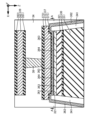
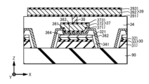
- FIG. 1 is a schematic cross-sectional view of a light emitting device according to a first embodiment of the present disclosure.
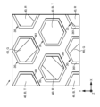
- FIG. 2 is an enlarged plan view of main parts of the light emitting device shown in FIG. 1.
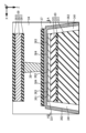
- FIG. 3 is an enlarged sectional view of a light emitting element that constructs the light emitting device shown in FIGS. 1 and 2.
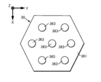
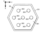
- FIG. 4 is a bottom view of essential parts showing the configuration of the first reflective layer and the first electrode of the light emitting element shown in FIG. 3.
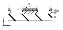
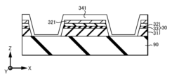
- FIG. FIG. 5 is a first step cross-sectional view corresponding to FIG. 3 illustrating the method for manufacturing the light emitting device according to the first embodiment.
- FIG. 6 is a sectional view of the second step.
- FIG. 7 is a sectional view of the third step.
- FIG. 1 is a schematic cross-sectional view of a light emitting device according to a first embodiment of the present disclosure.
- FIG. 2 is an enlarged plan view of main parts of the light emitting device shown in FIG.
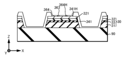
- FIG. 8 is a sectional view of the fourth step.
- FIG. 9 is a sectional view of the fifth step.
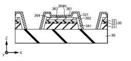
- FIG. 10 is a sectional view of the sixth step.
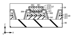
- FIG. 11 is a sectional view of the seventh step.
- FIG. 12 is a cross-sectional view of the eighth step.
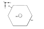
- FIG. 13 is a bottom view of essential parts showing the configuration of a first reflective layer and a first electrode of a light emitting element that constructs a light emitting device according to a second embodiment of the present disclosure.
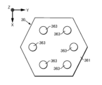
- FIG. 14 is a bottom view of essential parts showing the configuration of a first reflective layer and a first electrode of a light emitting element that constructs a light emitting device according to a first modification of the second embodiment.
- FIG. 14 is a bottom view of essential parts showing the configuration of a first reflective layer and a first electrode of a light emitting element that constructs a light emitting device according to a first modification of the second embodiment.
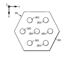
- FIG. 15 is a bottom view of essential parts showing the configuration of a first reflective layer and a first electrode of a light emitting element that constructs a light emitting device according to a second modification of the second embodiment.
- FIG. 16 is an enlarged sectional view corresponding to FIG. 3 of a light emitting element that constructs a light emitting device according to a third embodiment of the present disclosure.
- FIG. 17 is a bottom view of essential parts corresponding to FIG. 4, showing the configuration of the first reflective layer and the first electrode of the light emitting element shown in FIG. 16.
- FIG. 18 is an enlarged sectional view corresponding to FIG. 3 of a light emitting element that constructs a light emitting device according to a fourth embodiment of the present disclosure.
- FIG. 19 is a bottom view of essential parts corresponding to FIG.
- FIG. 20 is an enlarged sectional view corresponding to FIG. 3 of a light emitting element that constructs a light emitting device according to a fifth embodiment of the present disclosure.
- FIG. 21 is a block diagram showing an example of a schematic configuration of a vehicle control system.
- FIG. 22 is an explanatory diagram showing an example of the installation positions of the outside-vehicle information detection section and the imaging section.
- First Embodiment The first embodiment is a first example in which the present technology is applied to a light emitting device and a method for manufacturing the same. 2.
- Second Embodiment The second embodiment is a second example in which the structure of the light emitting element is changed in the light emitting device according to the first embodiment. 3.
- Third Embodiment The third embodiment is a third example in which the structure of the light emitting element is changed in the light emitting device according to the first embodiment or the second embodiment. 4.
- Fourth Embodiment The fourth embodiment is a fourth example in which the structure of the light emitting element is changed in the light emitting devices according to the first to third embodiments. 5.
- the fifth embodiment is a fifth example in which the structure of the light emitting element is changed in the light emitting devices according to the first to fourth embodiments. 6.
- Application Example to a Mobile Object This application example describes an example in which the present technology is applied to a vehicle control system, which is an example of a mobile object control system. 7.
- Other embodiments
- FIGS. 1 to 12 A light emitting device 1 and a method for manufacturing the same according to a first embodiment of the present disclosure will be described using FIGS. 1 to 12.
- the arrow X direction shown as appropriate is one plane direction when the light emitting device 1 is placed on a plane for convenience.
- the arrow Y direction is another plane direction orthogonal to the arrow X direction.
- the arrow Z direction is an upward direction orthogonal to the arrow X direction and the arrow Y direction.
- the arrow X direction, arrow Y direction, and arrow Z direction exactly correspond to the X-axis direction, Y-axis direction, and Z-axis direction of the three-dimensional coordinate system. Note that these directions are shown to aid understanding of the present technology, and do not limit the direction of the present technology.
- FIG. 1 shows an example of a schematic cross-sectional structure of the light emitting device 1 according to the first embodiment.
- FIG. 2 shows an example of a planar structure of the light emitting element 30 and color conversion layer 40 of the light emitting device 1.
- the light emitting device 1 includes a substrate region 2, a light emitter region 3, a color conversion region 4, and a filter region 5 in the longitudinal cross-sectional direction, which is the direction of arrow Z. and an optical system area 6. Further, the light emitting device 1 includes an element arrangement region 7 and a peripheral region 8 in the plane direction, which is the direction of the arrow X and the direction of the arrow Y.
- the light emitting device 1 mainly includes a substrate 20 included in the substrate region 2 and a light emitting body 35 disposed in the light emitter region 3 and including a plurality of light emitting elements 30 arranged in the element arrangement region 7. It is provided as an element.
- the substrate region 2 includes a substrate 20 and a drive circuit 21 mounted on the main surface of the substrate 20.
- the main surface of the substrate 20 is one main surface of the substrate 20 on which semiconductor elements (not shown) such as drive transistors are manufactured, and furthermore, the drive circuit 21 is constructed.
- a single crystal silicon (Si) substrate is used as the substrate 20.
- An insulator 201 is formed on the back and side surfaces of the substrate 20 opposite to the main surface.
- a silicon nitride (SiN) film or a silicon oxide (SiO) film can be practically used.
- the drive circuit 21 is constructed from a semiconductor element (not shown) formed on the main surface of the substrate 20.
- the drive transistor as a semiconductor element includes, for example, a complementary insulated gate field effect transistor (IGFET).
- Insulated gate field effect transistors include at least both field effect transistors (MISFETs) with metal/insulator/semiconductor structures and field effect transistors (MOSFETs) with metal/oxide/semiconductor structures.
- the drive circuit 21 is electrically connected to the first terminal 281 through the wiring layer 24.
- the wiring layer 24 here includes a plug wiring 240, a first layer wiring 241, a second layer wiring 242, a third layer wiring 243, a fourth layer wiring 244, and a plug wiring 245. We are prepared.
- the plug wiring 240 is formed on, for example, a main electrode of an insulated gate field effect transistor (not shown), and is electrically connected to this main electrode.
- dungsten W
- the first layer wiring 241 is formed on the plug wiring 240 and is electrically connected to the plug wiring 240.
- the second layer wiring 242 is formed on the first layer wiring 241 and is electrically connected to the first layer wiring 241.
- the third layer wiring 243 is formed on the second layer wiring 242 and is electrically connected to the second layer wiring 242.
- the fourth layer wiring 244 is formed on the third layer wiring 243 and is electrically connected to the third layer wiring 243.
- Each of the first layer wiring 241 to the fourth layer wiring 244 is formed with aluminum (Al) as a main composition, for example.
- the plug wiring 245 is formed in the fourth layer wiring 244 and is electrically connected to the fourth layer wiring 244 .
- the plug wiring 245 is made of the same material as the plug wiring 240, for example.
- an insulator 29 is provided in the wiring layer 24.
- the insulator 29 is formed around the plug wiring 240 and the plug wiring 245. Further, the insulator 29 is provided between the first layer wiring 241 and the second layer wiring 242, between the second layer wiring 242 and the third layer wiring 243, and between the third layer wiring 243 and the fourth layer wiring 243. It is formed between the layer wiring 244 and the like.
- the insulator 29 is formed of, for example, a SiO film or a SiN film.
- the light shielding film 26 is disposed closer to the drive circuit 21 than the light absorption film 27 is.
- the light shielding film 26 is configured to cover, for example, a drive transistor of the drive circuit 21.
- the light shielding film 26 is formed as an electrical path that electrically connects the drive circuit 21 and the first terminal 281, and is configured to block light leaking toward the drive circuit 21 side emitted from the light emitting element 30.
- the light shielding film 26 is formed of a single layer of metal whose main composition is, for example, Al, copper (Cu), W, or titanium (Ti).
- the light absorption film 27 is disposed on the light-emitting element 30 side of the light-shielding film 26.
- the light absorption film 27 is formed to have the same planar shape as the light shielding film 26 when viewed from the direction of arrow Z (hereinafter simply referred to as "planar view").
- the light absorption film 27 is formed as an electrical path that absorbs light leaking toward the drive circuit 21 side emitted from the light emitting element 30 and further electrically connects the drive circuit 21 and the first terminal 281.
- the light absorption film 27 is made of, for example, a metal or metal compound whose main composition is titanium nitride (TiN), cobalt (Co), nitrogen-doped titanium oxide (TiON), tantalum nitride (TaN), or amorphous carbon (a-C). It is formed from a single layer film.
- the first terminal 281 is electrically connected to the light absorption film 27 and disposed on the insulator 29.
- the first terminal 281 is configured to be electrically connected to one of the light emitting elements 30 (specifically, the second compound semiconductor layer 32).
- the first terminal 281 is made of, for example, Cu, which has a low resistance value.
- a second terminal 282 is provided on the insulator 29 .
- the second terminal 282 is configured to be electrically connected to the other side of the light emitting element 30 (specifically, the first compound semiconductor layer 31) or to the outside of the light emitting device 1.
- the second terminal 282 is formed on the same conductive layer as the light shielding film 26 and the light absorption film 27, and is formed of the same conductive material.
- the light emitter region 3 is on the substrate region 2 and includes a light emitter 35 disposed on the insulator 29.
- the light emitting body 35 is configured by arranging a plurality of light emitting elements 30 formed from a compound semiconductor layer in a matrix along the direction of the light emitting surface of the light emitting element 30 (arrow X direction and arrow Y direction).
- the light emitting element 30 is formed in a hexagonal shape when viewed from above.
- the light emitting elements 30 are arranged in the direction of the arrow X and in a direction inclined by 30 degrees toward the direction of the arrow X with respect to the direction of the arrow Y (direction of the arrow Y).
- the light emitting element 30 includes a light emitting element 30 (R) that emits red light, which is the three primary colors of light, a light emitting element 30 (B) that emits blue light, and a light emitting element 30 (G) that emits green light.
- the light emitting elements 30(R), 30(B), and 30(G) are arranged with their centers exactly aligned with the vertices of an equilateral triangle. That is, in the first embodiment, each of the light emitting elements 30 (R), the light emitting elements 30 (B), and the light emitting elements 30 (G) are arranged in a delta arrangement.
- the light emitter 35 further includes an insulator 34 formed around the plurality of light emitting elements 30 except for the light emitting surface.
- the insulator 34 is formed mainly of a SiO film or a SiN film.
- FIG. 3 shows an example of an enlarged cross-sectional configuration of the light-emitting element 30 that constructs the light-emitting device 1.
- FIG. 4 shows an example of the configuration of the first reflective layer 361 and the first electrode 363 of the light emitting element 30.
- FIG. 4 is a bottom view taken along the line AA shown in FIG. 3 and viewed from the direction opposite to the direction of arrow Z. Note that the bottom view corresponding to FIG. 4 used in the second embodiment and later described below is a bottom view cut at the same position.
- the light emitting element 30 is configured as a light emitting diode (LED) including a first compound semiconductor layer 31, a second compound semiconductor layer 32, and an active layer 33.
- LED light emitting diode
- the light emitting element 30 is formed mainly of a III-V compound semiconductor, for example.
- the first compound semiconductor layer 31 is disposed on the color conversion region 4 side and on the light emission side.
- the first compound semiconductor layer 31 is made of, for example, n-type gallium nitride (n-GaN).
- n type is the "first conductivity type” according to the present technology.
- the second compound semiconductor layer 32 is provided on the substrate region 2 side.
- the second compound semiconductor layer 32 is made of, for example, p-type gallium nitride (p-GaN).
- p type is a "second conductivity type” opposite to the first conductivity type according to the present technology.
- the active layer 33 is disposed between the first compound semiconductor layer 31 and the second compound semiconductor layer 32. In other words, the active layer 33 is stacked on the first compound semiconductor layer 31, and the second compound semiconductor layer 32 is stacked on the side of the active layer 33 opposite to the first compound semiconductor layer 31.
- the active layer 33 is formed as a light emitting layer that emits light. Although not limited to this, in the first embodiment, the light emitting element 30 emits blue light.
- the light emitting element 30 In one light emitting element 30, at least a portion of the first compound semiconductor layer 31, the active layer 33, and the second compound semiconductor layer 32 have a mesa-shaped cross section. That is, as described above, the light emitting element 30 is formed in a hexagonal shape when viewed from above, and is formed into a mesa shape when viewed in the direction of arrow Y (hereinafter simply referred to as "in side view"). Note that the planar shape of the light emitting element 30 is not limited to a hexagonal shape. The planar shape of the light emitting element 30 may be, for example, circular, rectangular, or the like.
- the transparent electrode 321 is provided on the surface of the second compound semiconductor layer 32 on the substrate region 2 side.
- the transparent electrode 321 is electrically connected to substantially the entire surface of the second compound semiconductor layer 32 .
- the transparent electrode 321 is formed for each light emitting element 30, and is formed to have the same planar shape as the second compound semiconductor layer 32 in plan view.
- the transparent electrode 321 is made of, for example, indium tin oxide (ITO). Thereby, the transparent electrode 321 is connected to the second compound semiconductor layer 32 through ohmic contact.
- ITO indium tin oxide
- each of the plurality of light emitting elements 30 includes a first reflective layer 361, a first electrode 363, an insulator 364, a second reflective A layer 362 and a second electrode 37 are provided.
- first reflective layer 361 will be explained in detail.
- the first reflective layer 361 is disposed over the entire area of the second compound semiconductor layer 32 on the substrate region 2 side, with the transparent electrode 321 interposed therebetween, and spaced apart from the second compound semiconductor layer 32 .
- the first reflective layer 361 is disposed over the entire area of the transparent electrode 321 on the substrate region 2 side, apart from the transparent electrode 321 .
- the first reflective layer 361 is made of a metal material that is conductive and has a high light reflectance of 75% or more for blue light with a wavelength of 400 nm, for example. That is, the first reflective layer 361 is configured to supply the second compound semiconductor layer 32 with the current necessary for light emission of the light emitting element 30 and to reliably reflect the light emitted from the active layer 33.
- the first reflective layer 361 is made of, for example, Al (preferably pure Al).
- Al has a reflectance of 92.5% for blue light when the thickness is 75 nm. Further, for blue light, the reflectance starts to decrease when the thickness of Al becomes less than 50 nm. For this reason, the thickness of the first reflective layer 361 is formed to be, for example, 50 nm or more, and 100 nm or less from a manufacturing standpoint.
- the first reflective layer 361 may be formed of one or more materials other than Al, such as selected from Al alloy, Ag, and Ag alloy.
- the light emitted from the active layer 33 passes through the second compound semiconductor layer 32, reaches the first reflective layer 361, and is reflected by the first reflective layer 361.
- the reflected light passes through each of the second compound semiconductor layer 32, the active layer 33, and the first compound semiconductor layer 31, and is emitted. Therefore, the light before and after reflection from the first reflective layer 361 is not attenuated by interference, but is instead amplified, and the thickness of the second compound semiconductor layer 32 is set to a thickness that ultimately amplifies the light extraction efficiency. is set.
- the first electrode 363 is disposed between the second compound semiconductor layer 32 and the first reflective layer 361.
- the first electrode 363 is disposed between the transparent electrode 321 and the first reflective layer 361.
- the first electrode 363 is configured to electrically connect a portion of each of the second compound semiconductor layer 32 or the transparent electrode 321, and the first reflective layer 361.
- the first electrode 363 is used as a contact metal. In contrast to the direct connection between the first reflective layer 361 and the transparent electrode 321, when the first reflective layer 361 is connected to the transparent electrode 321 with the first electrode 363 interposed, good electrical continuity can be obtained.
- the first electrode 363 is made of, for example, Ti or a Ti alloy.
- the thickness of the first electrode 363 is, for example, 10 nm or more and 100 nm or less.
- first electrodes 363 are provided for one first reflective layer 361 in plan view.
- the first electrode 363 has a circular planar shape.
- One first electrode 363 is arranged at the center position of the first reflective layer 361 having a hexagonal shape in plan view, and six first electrodes 363 are arranged at equal intervals at peripheral positions corresponding to each of the contour corners of the first reflective layer 361. are arranged.
- the total area of the seven first electrodes 363 when viewed from the thickness direction is smaller than the area of the first reflective layer 361 when viewed from the same direction.
- the total area of the first electrodes 363 is set to be 1% or more and 30% or less of the area of the first reflective layer 361.
- the voltage drop due to the first electrode 363 is suppressed to, for example, 10 mV or less, and the drive current of the light emitting element 30 is not affected. Further, the reflectance of the first electrode 363 is lower than the reflectance of the first reflective layer 361. In other words, since the area of the first electrode 363 covering the first reflective layer 361 is small, the area of the first reflective layer 361 contributing to reflection increases, and the decrease in light extraction efficiency can be suppressed to 30% or less.
- planar shape of the first electrode 363 is not limited to a circular shape.
- the planar shape of the first electrode 363 may be an ellipse, a triangle, a rectangle, a polygon of pentagon or more, a slit, or the like.
- the insulator 364 is disposed around the first electrode 363 between the first reflective layer 361 and the transparent electrode 321. In other words, the insulator 364 is disposed between the first reflective layer 361 and the transparent electrode 321, except for the region where the first electrode 363 is disposed.
- the insulator 364 has light transmittance and insulation properties, and is used as a barrier layer that separates the first reflective layer 361 and the transparent electrode 321.
- the insulator 364 is made of, for example, aluminum oxide (AlO) or SiO.
- the thickness of the insulator 364 is effectively the same as the thickness of the first electrode 363.
- the insulator 364 is formed by, for example, an atomic layer deposition (ALD) method.
- the second reflective layer 362 includes the first compound semiconductor layer 31, the active layer 33, and the second compound semiconductor layer in side view. 32 along and surrounding the side surfaces of the mesa shape.
- An insulator 341 is formed between the second reflective layer 362 and the first compound semiconductor layer 31, active layer 33, and second compound semiconductor layer 32.
- the insulator 341 is made of, for example, SiO or SiN.
- the second reflective layer 362 reflects the light emitted from the active layer 33 and the light reflected from the first reflective layer 361 toward the first compound semiconductor layer 31 side, thereby improving light extraction efficiency.
- the second reflective layer 362 is formed in the same layer and made of the same material as the first reflective layer 361. Furthermore, the second reflective layer 362 is formed continuously and integrally with the first reflective layer 361.
- the second electrode 37 is formed on the opposite side of the first reflective layer 361 from the second compound semiconductor layer 32 . As shown in FIG. 3, the second electrode 37 is formed over the entire area of the first reflective layer 361 and has an area slightly larger than the area of the first reflective layer 361 in plan view and side view. There is.
- the second electrode 37 is electrically connected to the second compound semiconductor layer 32 via the first reflective layer 361, the first electrode 363, and the transparent electrode 321, respectively.
- the second electrode 37 is formed by sequentially laminating a barrier metal layer 371, an Al alloy layer 372, and a barrier metal layer 373.
- the barrier metal layer 371 is made of, for example, titanium nitride (TiN), and has a thickness of 10 nm or more and 100 nm or less.
- TiN titanium nitride
- AlCu which is Al with Cu added thereto
- AlSi which is Al with Si added
- the amount of Cu added is, for example, 1% or more and 3% or less.
- the amount of Si added is, for example, 1% or more and 5% or less.
- the Al alloy layer 372 is formed to have a thickness of, for example, 300 nm or more and 800 nm or less.
- the barrier metal layer 373 is made of, for example, TiN, and has a thickness of 10 nm or more and 100 nm or less.
- Plug Wiring 38 One end of the plug wiring 38 is electrically connected to the second electrode 37, and the other end of the plug wiring 38 is electrically connected to the wiring 39.
- the plug wiring 38 is disposed at the center of the first reflective layer 361 and is formed to penetrate the insulator 34.
- the plug wiring 38 is made of W, for example.
- the wiring 39 is formed by sequentially laminating a barrier metal layer 391, an Al alloy layer 392, and a barrier metal layer 393.
- the barrier metal layer 391 is made of, for example, TiN, like the barrier metal layer 371.
- the barrier metal layer 391 is formed to have a thickness of, for example, 10 nm or more and 100 nm or less.
- the Al alloy layer 392 is made of, for example, AlCu or AlSi.
- the Al alloy layer 392 is formed with a thickness of, for example, 500 nm or more and 600 nm or less.
- the barrier metal layer 393 is made of, for example, TiN, and has a thickness of, for example, 10 nm or more and 100 nm or less.
- each of the barrier metal layer 391 and the barrier metal layer 393 of the wiring 39 may be formed of a composite film in which Ti, TiN, and Ti are sequentially laminated, instead of TiN.
- Ti is formed to have a thickness of, for example, 30 nm or less.
- TiN is formed to have a thickness of, for example, 10 nm or more and 100 nm or less.
- the wiring 39 is connected to the third terminal 390 of the light emitter region 3.
- the third terminal 390 is formed on the surface of the insulator 34 on the substrate region 2 side.
- the third terminal 390 is made of, for example, Cu, like the first terminal 281 described above.
- the third terminal 390 is joined to the first terminal 281 and is electrically connected to the first terminal 281.
- a second reflective layer 362 is disposed between the second reflective layer 34 and the second reflective layer 362 .
- the insulator 34 and the second reflective layer 362 construct an element isolation region 300 that optically isolates adjacent light emitting elements 30.
- the transparent electrode 311 is disposed on the opposite side of the first compound semiconductor layer 31 of the light emitting element 30 from the second compound semiconductor layer 32. There is.
- the transparent electrode 311 is electrically connected to the first compound semiconductor layer 31.
- the transparent electrode 311 is made of the same material as the transparent electrode 321 described above.
- a wiring 312 that supplies current to the first compound semiconductor layer 31 through the transparent electrode 311 is electrically connected to the transparent electrode 311 .
- the wiring 312 is made of W, for example.
- the color conversion area 4 includes a color conversion layer 40, a third reflective layer 401, and partition walls 41.
- the color conversion layer 40 is disposed on the light emitting surface of the light emitting element 30, that is, on the transparent electrode 311, with an insulator (not shown) interposed therebetween.
- the color conversion layer 40 is provided for each light emitting element 30.
- the color conversion layer 40 converts the light emitted from the light emitting element 30 into a specific color.
- the light emitting element 30 is configured to emit blue light, as described above.
- a color conversion layer 40 (R) that converts blue light to red light, a color conversion layer 40 (G) that converts blue light to green light, and a transparent color conversion layer 40 (B) that allows blue light to pass through as is. , T) are provided.
- the color conversion layer 40 is made of, for example, a resin material.
- the light emitting device 1 according to the first embodiment configured as described above is constructed as a color light emitting device. More practically, the light-emitting device 1 is constructed as a color image display device or as a micro-light-emitting device (micro-LED).
- the third reflective layer 401 is disposed along the periphery of the side surface of the color conversion layer 40.
- the third reflective layer 401 reflects the light emitted from the light emitting element 30 and the light diffused from the color conversion layer 40, thereby improving light extraction efficiency.
- the third reflective layer 401 is made of, for example, the same material as the first reflective layer 361.
- partition walls 41 are formed between the color conversion layers 40 adjacent in the planar direction and between the adjacent third reflective layers 401.
- the partition wall 41 is configured to optically separate the color conversion layers 40 and to hold the color conversion layers 40.
- the partition wall 41 is made of, for example, SiO or SiN.
- a filter area 5 is arranged on the color conversion area 4.
- a distributed reflection layer (DBR: Distributed Bragg Reflector) 50 and a color filter 51 are sequentially laminated from the color conversion region 4 side.
- the distributed reflection layer 50 reflects light of a specific color.
- Color filter 51 absorbs light of a specific color.
- the specific emitted light color is, for example, blue light.
- the optical system area 6 On the filter area 5, the optical system area 6 is arranged.
- An on-chip lens 60 is provided in the optical system area 6.
- the optical lens has a cross-sectional shape that protrudes and curves in the light emission direction.
- the on-chip lens 60 is made of, for example, a resin material or an inorganic material.
- a support substrate 90 is prepared (see FIG. 5).
- a sapphire substrate is used as the support substrate 90.
- a first compound semiconductor layer (n-GaN) 31, an active layer 33, and a second compound semiconductor layer (p-GaN) 32 are sequentially formed on the support substrate 90 (see FIG. 5).
- a transparent electrode 321 is formed on the second compound semiconductor layer 32 (see FIG. 5).
- a mask 901 is formed on the transparent electrode 321.
- Mask 901 is used as an etching mask for forming a mesa shape.
- the mask 901 is formed of, for example, a single layer film of SiO, SiN, etc., or a composite film containing them.
- the transparent electrode 321, the second compound semiconductor layer 32, the active layer 33, and the first compound semiconductor layer 31 are etched using the mask 901.
- the transparent electrode 321, the second compound semiconductor layer 32, the active layer 33, and the first compound semiconductor layer 31 are formed into a mesa shape.
- dry etching is used for the etching.
- mask 901 is removed.
- an insulator 341 is formed along the top and side surfaces of the mesa shape.
- the insulator 341 is formed using, for example, a chemical vapor deposition (CVD) method.
- an opening 341H is formed in a part of the insulator 341 on the upper surface of the mesa shape, and the surface of the transparent electrode 321 is exposed (see FIG. 8).
- the opening 341H is formed using photolithography and etching techniques.
- an insulator 364 is formed on the transparent electrode 321 within the opening 341H (see FIGS. 9 and 3).
- the insulator 364 is made of AlO or SiO, for example, as described above.
- the insulator 364 is formed by, for example, an ALD method.
- an opening 364H is formed in the insulator 364 in the region where the first electrode 363 is formed, and the surface of the transparent electrode 321 is exposed (see FIGS. 9 and 3).
- the opening 364H is formed using, for example, photolithography and etching techniques.
- a first electrode 363 is formed in the opening 341H to be electrically connected to a portion of the surface of the transparent electrode 321 through the opening 364H.
- the first electrode 363 is made of, for example, Ti or a Ti alloy.
- the first electrode 363 is formed into a film using, for example, a sputtering method, and then patterned using an etching technique to form a predetermined shape. Note that in FIGS. 8 to 12, one first electrode 363 is shown in order to simplify the cross-sectional shape, but as shown in FIG. 4 described above, the first electrode 363 is Seven pieces are arranged in this form.
- a first reflective layer 361 is formed on the first electrode 363 and the insulator 364 within the opening 341H. Then, in the same manufacturing process as the first reflective layer 361, a second reflective layer 362 is formed on the insulator 341 along the mesa-shaped sidewall.
- the first reflective layer 361 and the second reflective layer 362 are formed of Al deposited using a CVD method, for example.
- a second electrode 37 is formed on the first reflective layer 361.
- the second electrode 37 is formed by sequentially stacking the barrier metal layer 371, the Al alloy layer 372, and the barrier metal layer 373. These are deposited using, for example, a sputtering method, and patterned using an etching technique after the deposition.
- an insulator 34 embedding the second electrode 37 is formed.
- a plug wiring 38 is formed on the insulator 34, and a wiring 39 is formed on the insulator 34, as shown in FIG.
- the light emitting device 30 is substantially completed. Thereafter, as shown in FIG. 1 described above, the third terminal 390 is formed on the light emitting element 30. After bonding the substrate region 2, the light emitting element 30 is peeled off from the support substrate 90. After peeling, the color conversion region 4, filter region 5, and optical system region 6 are each formed in sequence, and the light emitting device 1 according to the first embodiment is completed.
- the light emitting device 1 includes a first compound semiconductor layer 31, an active layer 33, a second compound semiconductor layer 32, and a first reflective layer 31.
- a layer 361 and a first electrode 363 are provided.
- the first compound semiconductor layer 31 has a first conductivity type.
- the active layer 33 is stacked on the first compound semiconductor layer 31 .
- the second compound semiconductor layer 32 is stacked on the side of the active layer 33 opposite to the first compound semiconductor layer 31, and has a second conductivity type opposite to the first conductivity type.
- the first reflective layer 361 is spaced apart from the surface of the second compound semiconductor layer 32 opposite to the active layer 33 and reflects light emitted from the active layer 33 .
- the first electrode 363 is disposed between the second compound semiconductor layer 32 and the first reflective layer 361 and electrically connects a portion of each of the second compound semiconductor layer 32 and the first reflective layer 361. do.
- the first reflective layer 361 is provided on the surface of the second compound semiconductor layer 32, so that light emitted from the active layer 33 is prevented from leaking to the drive circuit 21 side. can be effectively suppressed or prevented.
- the first reflective layer 361 is disposed over the entire surface of the second compound semiconductor layer 32, there is no light leakage. Since the first reflective layer 361 can reflect light efficiently, the light extraction efficiency of the light emitting device 1 can be improved.
- the image quality of the image display device can be improved. Furthermore, since the first reflective layer 361 is connected to the second compound semiconductor layer 32 with the first electrode 363 interposed, the supply of current from the first reflective layer 361 side is improved, and the luminous efficiency of the light emitting element 30 is improved. can be improved. In addition, since the first electrode 363 is electrically connected to a portion of each of the first reflective layer 361 and the second compound semiconductor layer 32, a sufficient reflective area of the first reflective layer 361 can be ensured. Can be done. Therefore, the light emitting device 1 can further improve the light extraction efficiency. Furthermore, since the first reflective layer 361 can block light leakage to the drive circuit 21 side, malfunctions of the drive circuit 21 due to light leakage can be effectively suppressed or prevented. Therefore, the operational reliability of the light emitting device 1 can be improved.
- the first reflective layer 361 is made of one or more materials selected from Al, Al alloy, Ag, and Ag alloy.
- the thickness of the first reflective layer 361 is 75 nm
- the reflectance of blue light having a wavelength of 400 nm is 92.5% for Al and 91.5% for Al alloy (AlCu).
- 86.2% for Ag and 84.0% for Ag alloy is 86.2% for Ag and 84.0% for Ag alloy. That is, since the reflectance of the first reflective layer 361 is set to 75% or more, the light extraction efficiency of the light emitting device 1 can be further improved.
- the light emitting device 1 further includes a transparent electrode 321 between the second compound semiconductor layer 32 and the first electrode 363, as shown in FIG. and is electrically connected to the second compound semiconductor layer 32. Therefore, a good electrical connection between the second compound semiconductor layer 32 and the transparent electrode 321 can be obtained, and as a result, a good electrical connection can be obtained between the first reflective layer 361 and the second compound semiconductor layer 32. .
- the first electrode 363 is made of Ti or a Ti alloy. Therefore, good electrical connection between the first reflective layer 361 and the transparent electrode 321 can be obtained.
- the total area of the first electrode 363 viewed from the thickness direction is smaller than the area of the first reflective layer 361 viewed from the same direction.
- the total area of the first electrodes 363 is 1% or more and 30% or less of the area of the first reflective layer 361.
- the first electrode 363 is formed with such an area ratio, the voltage drop due to the first electrode 363 is suppressed, and the drive current of the light emitting element 30 is not affected.
- the area of the first electrode 363 that covers the first reflective layer 361 is reduced, and the reflective area of the first reflective layer 361 can be increased, so that light extraction efficiency can be improved.
- the light emitting device 1 also includes a transparent electrode 321 and a first reflective layer between the second compound semiconductor layer 32 and the first reflective layer, specifically, excluding the first electrode 363
- An insulator 364 is provided between the reflective layer 361 and the reflective layer 361 .
- the insulator 364 has optical transparency and insulating properties. Therefore, compositional changes in the first reflective layer 361 caused by the transparent electrode 321 can be effectively suppressed or prevented, so that the reflectance of the first reflective layer 361 can be maintained and the light extraction efficiency can be improved. can.
- the second compound semiconductor layer 32 is formed to have a thickness that increases the light extraction efficiency.
- the second compound semiconductor layer 32 has an appropriate thickness so that the light emitted from the active layer 33 toward the first compound semiconductor layer 31 is not attenuated by the light that is reflected by the first reflective layer 361 and reaches the active layer 33. It is formed. In the light emitting device 1 configured in this manner, light extraction efficiency can be improved.
- the light emitting device 1 as particularly shown in FIG. 3, at least a portion of the first compound semiconductor layer 31, the active layer 33, and the second compound semiconductor layer 32 have a mesa shape.
- a second reflective layer 362 is disposed along the side surface of the mesa shape. The second reflective layer 362 reflects the light emitted from the active layer 33 and the light reflected from the first reflective layer 361 toward the first compound semiconductor layer 31 side. Therefore, in the light emitting device 1, light can be extracted efficiently by the second reflective layer 362, so that the light extraction efficiency can be further improved.
- the second reflective layer 362 is formed in the same layer and made of the same material as the first reflective layer 361.
- the second reflective layer 362 is integrally formed with the first reflective layer 361. Therefore, the structure of the light emitting device 1 can be simplified.
- the first reflective layer 361 and the second reflective layer 362 are formed in the same process. Therefore, one of the originally required steps of forming the first reflective layer 361 and the second reflective layer 362 can be omitted, which reduces the number of manufacturing steps in the method of manufacturing the light emitting device 1. be able to.
- the light emitting device 1 includes a second electrode 37, as shown in FIGS. 1 and 3.
- the second electrode 37 is disposed on the opposite side of the first reflective layer 361 from the second compound semiconductor layer 32 .
- the second electrode 37 is formed by sequentially stacking a barrier metal layer 371, an Al alloy layer 372, and a barrier metal layer 373.
- the second electrode 37 configured in this manner can improve electrical reliability as an electrode.
- Second embodiment> A light emitting device 1 according to a second embodiment of the present disclosure will be described using FIGS. 13 to 15. Note that in the second embodiment and subsequent embodiments, the same or substantially the same components as those of the light emitting device 1 according to the first embodiment are denoted by the same reference numerals. However, duplicate explanations will be omitted.
- FIG. 13 shows an example of the configuration of the first reflective layer 361 and first electrode 363 of the light emitting element 30 in the light emitting device 1 according to the second embodiment.
- one first electrode 363 is disposed at the center of the first reflective layer 361 of the light emitting element 30 in plan view.
- the total area ratio of the first electrode 363 to the first reflective layer 361 is the same as the area ratio of the light emitting device 1 according to the first embodiment.
- the planar shape of the first electrode 363 is the same as the planar shape of the first electrode 363 of the light emitting device 1 according to the first embodiment.
- FIG. 14 shows an example of the configuration of the first reflective layer 361 and the first electrode 363 of the light emitting element 30 in the light emitting device 1 according to the first modification of the second embodiment.
- a total of four first electrodes 363, two in the direction of the arrow X and two in the direction of the arrow Y, are arranged on the first reflective layer 361. It is set up. Components other than those described above are the same as those of the light emitting device 1 according to the first embodiment, so description thereof will be omitted here.
- FIG. 15 shows an example of the configuration of the first reflective layer 361 and the first electrode 363 of the light emitting element 30 in the light emitting device 1 according to the second modification of the second embodiment.
- the first electrode 363 is located at peripheral positions corresponding to each of the contour corners of the first reflective layer 361, which has a hexagonal shape in plan view. Six pieces are placed at intervals. Components other than those described above are the same as those of the light emitting device 1 according to the first embodiment, so description thereof will be omitted here.
- FIG. 16 shows an example of an enlarged cross-sectional configuration of the light emitting element 30 that constructs the light emitting device 1 according to the third embodiment.
- FIG. 17 shows an example of the configuration of the first reflective layer 361 and the first electrode 363 of the light emitting element 30.
- a transparent electrode 321 (see FIG. 3) is provided between the second compound semiconductor layer 32 and the first reflective layer 361 of the light emitting element 30. ) is not provided.
- the first reflective layer 361 is directly connected to the second compound semiconductor layer 32 with a first electrode 363 interposed therebetween. Since the transparent electrode 321 is not provided, the first electrode 363 is made of, for example, Ni, Pd, or Cr. These materials are materials that can be electrically connected to the second compound semiconductor layer 32 with low resistance. In other words, the first electrode 363 achieves good electrical continuity with the second compound semiconductor layer 32.
- the first electrodes 363 are formed in the same arrangement and number as the first electrodes 363 shown in FIG. 4 of the light emitting device 1 according to the first embodiment. Note that the first electrodes 363 may be formed in the same arrangement and number as the first electrodes 363 shown in each of FIGS. 13, 14, and 15 of the light emitting device 1 according to the second embodiment.
- FIG. 18 shows an example of an enlarged cross-sectional configuration of the light emitting element 30 that constructs the light emitting device 1 according to the fourth embodiment.
- FIG. 19 shows an example of the configuration of the first reflective layer 361 and the first electrode 363 of the light emitting element 30.
- the second reflective layer 362 is electrically isolated from the first reflective layer 361.
- an insulator 342 is formed between the second reflective layer 362 and the first reflective layer 361.
- the second reflective layer 362 is in an electrically floating state.
- the second reflective layer 362 is formed in the same layer as the first reflective layer 361 and made of the same material, similarly to the second reflective layer 362 of the light emitting device 1 according to the first embodiment described above. ing. Further, the second reflective layer 362 may be formed as a separate layer from the first reflective layer 361 and may be formed of a different material.
- the second reflective layer 362 is electrically isolated from the first reflective layer 361.
- the second compound semiconductor layer 32, the active layer 33, and the first compound semiconductor layer 31 are connected to one electrode, and the insulator 341 is connected to the current path from the first reflective layer 361 to the second compound semiconductor layer 32.
- No parasitic capacitance is added using the dielectric and the second reflective layer 362 as the other electrode. Therefore, the driving operation speed of the light emitting element 30 can be increased.
- FIG. 20 shows an example of an enlarged cross-sectional configuration of the light emitting element 30 that constructs the light emitting device 1 according to the fifth embodiment.
- the second electrode 37 is disposed on the first reflective layer 361, similarly to the light emitting device 1 according to the first embodiment. .
- the second electrode 37 is different from the second electrode 37 of the light emitting device 1 according to the first embodiment, and is formed of a single barrier metal layer.
- TiN is used as the barrier metal layer.
- the first reflective layer 361 may be formed of an Al alloy, although there is a slight decrease in reflectance.
- Al alloy for example, AlCu can be practically used.
- the second electrode 37 is formed of a single barrier metal layer, so that the structure can be simplified.
- the technology according to the present disclosure (this technology) can be applied to various products.
- the technology according to the present disclosure may be realized as a device mounted on any type of moving body such as a car, electric vehicle, hybrid electric vehicle, motorcycle, bicycle, personal mobility, airplane, drone, ship, robot, etc. It's okay.
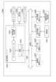
- FIG. 21 is a block diagram showing a schematic configuration example of a vehicle control system, which is an example of a mobile object control system to which the technology according to the present disclosure can be applied.
- the vehicle control system 12000 includes a plurality of electronic control units connected via a communication network 12001.
- the vehicle control system 12000 includes a drive system control unit 12010, a body system control unit 12020, an outside vehicle information detection unit 12030, an inside vehicle information detection unit 12040, and an integrated control unit 12050.
- a microcomputer 12051, an audio/image output section 12052, and an in-vehicle network I/F (Interface) 12053 are illustrated as the functional configuration of the integrated control unit 12050.
- the drive system control unit 12010 controls the operation of devices related to the drive system of the vehicle according to various programs.
- the drive system control unit 12010 includes a drive force generation device such as an internal combustion engine or a drive motor that generates drive force for the vehicle, a drive force transmission mechanism that transmits the drive force to wheels, and a drive force transmission mechanism that controls the steering angle of the vehicle. It functions as a control device for a steering mechanism to adjust and a braking device to generate braking force for the vehicle.
- the body system control unit 12020 controls the operations of various devices installed in the vehicle body according to various programs.
- the body system control unit 12020 functions as a keyless entry system, a smart key system, a power window device, or a control device for various lamps such as a headlamp, a back lamp, a brake lamp, a turn signal, or a fog lamp.
- radio waves transmitted from a portable device that replaces a key or signals from various switches may be input to the body control unit 12020.
- the body system control unit 12020 receives input of these radio waves or signals, and controls the door lock device, power window device, lamp, etc. of the vehicle.
- the external information detection unit 12030 detects information external to the vehicle in which the vehicle control system 12000 is mounted.
- an imaging section 12031 is connected to the outside-vehicle information detection unit 12030.
- the vehicle exterior information detection unit 12030 causes the imaging unit 12031 to capture an image of the exterior of the vehicle, and receives the captured image.
- the external information detection unit 12030 may perform object detection processing such as a person, car, obstacle, sign, or text on the road surface or distance detection processing based on the received image.
- the imaging unit 12031 is an optical sensor that receives light and outputs an electrical signal according to the amount of received light.
- the imaging unit 12031 can output the electrical signal as an image or as distance measurement information.
- the light received by the imaging unit 12031 may be visible light or non-visible light such as infrared rays.
- the in-vehicle information detection unit 12040 detects in-vehicle information.
- a driver condition detection section 12041 that detects the condition of the driver is connected to the in-vehicle information detection unit 12040.
- the driver condition detection unit 12041 includes, for example, a camera that images the driver, and the in-vehicle information detection unit 12040 detects the degree of fatigue or concentration of the driver based on the detection information input from the driver condition detection unit 12041. It may be calculated, or it may be determined whether the driver is falling asleep.
- the microcomputer 12051 calculates control target values for the driving force generation device, steering mechanism, or braking device based on the information inside and outside the vehicle acquired by the vehicle exterior information detection unit 12030 or the vehicle interior information detection unit 12040, Control commands can be output to 12010.
- the microcomputer 12051 realizes ADAS (Advanced Driver Assistance System) functions, including vehicle collision avoidance or impact mitigation, following distance based on vehicle distance, vehicle speed maintenance, vehicle collision warning, vehicle lane departure warning, etc. It is possible to perform cooperative control for the purpose of ADAS (Advanced Driver Assistance System) functions, including vehicle collision avoidance or impact mitigation, following distance based on vehicle distance, vehicle speed maintenance, vehicle collision warning, vehicle lane departure warning, etc. It is possible to perform cooperative control for the purpose of
- ADAS Advanced Driver Assistance System
- the microcomputer 12051 controls the driving force generating device, steering mechanism, braking device, etc. based on information about the surroundings of the vehicle acquired by the vehicle exterior information detection unit 12030 or the vehicle interior information detection unit 12040. It is possible to perform cooperative control for the purpose of autonomous driving, etc., which does not rely on operation.
- the microcomputer 12051 can output a control command to the body system control unit 12030 based on the information outside the vehicle acquired by the outside information detection unit 12030.
- the microcomputer 12051 controls the headlamps according to the position of the preceding vehicle or oncoming vehicle detected by the vehicle exterior information detection unit 12030, and performs cooperative control for the purpose of preventing glare, such as switching from high beam to low beam. It can be carried out.
- the audio and image output unit 12052 transmits an output signal of at least one of audio and images to an output device that can visually or audibly notify information to the occupants of the vehicle or to the outside of the vehicle.
- an audio speaker 12061, a display section 12062, and an instrument panel 12063 are illustrated as output devices.
- the display unit 12062 may include, for example, at least one of an on-board display and a head-up display.
- FIG. 22 is a diagram showing an example of the installation position of the imaging section 12031.
- the imaging unit 12031 includes imaging units 12101, 12102, 12103, 12104, and 12105.
- the imaging units 12101, 12102, 12103, 12104, and 12105 are provided at, for example, the front nose of the vehicle 12100, the side mirrors, the rear bumper, the back door, and the upper part of the windshield inside the vehicle.
- An imaging unit 12101 provided in the front nose and an imaging unit 12105 provided above the windshield inside the vehicle mainly acquire images in front of the vehicle 12100.
- Imaging units 12102 and 12103 provided in the side mirrors mainly capture images of the sides of the vehicle 12100.
- An imaging unit 12104 provided in the rear bumper or back door mainly captures images of the rear of the vehicle 12100.
- the imaging unit 12105 provided above the windshield inside the vehicle is mainly used to detect preceding vehicles, pedestrians, obstacles, traffic lights, traffic signs, lanes, and the like.
- FIG. 22 shows an example of the imaging range of the imaging units 12101 to 12104.
- An imaging range 12111 indicates the imaging range of the imaging unit 12101 provided on the front nose
- imaging ranges 12112 and 12113 indicate imaging ranges of the imaging units 12102 and 12103 provided on the side mirrors, respectively
- an imaging range 12114 shows the imaging range of the imaging unit 12101 provided on the front nose.
- the imaging range of the imaging unit 12104 provided in the rear bumper or back door is shown. For example, by overlapping the image data captured by the imaging units 12101 to 12104, an overhead image of the vehicle 12100 viewed from above can be obtained.
- At least one of the imaging units 12101 to 12104 may have a function of acquiring distance information.
- at least one of the imaging units 12101 to 12104 may be a stereo camera including a plurality of image sensors, or may be an image sensor having pixels for phase difference detection.
- the microcomputer 12051 determines the distance to each three-dimensional object within the imaging ranges 12111 to 12114 and the temporal change in this distance (relative speed with respect to the vehicle 12100) based on the distance information obtained from the imaging units 12101 to 12104. By determining the following, it is possible to extract, in particular, the closest three-dimensional object on the path of vehicle 12100, which is traveling at a predetermined speed (for example, 0 km/h or more) in approximately the same direction as vehicle 12100, as the preceding vehicle. can. Furthermore, the microcomputer 12051 can set an inter-vehicle distance to be secured in advance in front of the preceding vehicle, and perform automatic brake control (including follow-up stop control), automatic acceleration control (including follow-up start control), and the like. In this way, it is possible to perform cooperative control for the purpose of autonomous driving, etc., in which the vehicle travels autonomously without depending on the driver's operation.
- automatic brake control including follow-up stop control
- automatic acceleration control including follow-up start control
- the microcomputer 12051 transfers three-dimensional object data to other three-dimensional objects such as two-wheeled vehicles, regular vehicles, large vehicles, pedestrians, and utility poles based on the distance information obtained from the imaging units 12101 to 12104. It can be classified and extracted and used for automatic obstacle avoidance. For example, the microcomputer 12051 identifies obstacles around the vehicle 12100 into obstacles that are visible to the driver of the vehicle 12100 and obstacles that are difficult to see. Then, the microcomputer 12051 determines a collision risk indicating the degree of risk of collision with each obstacle, and when the collision risk exceeds a set value and there is a possibility of a collision, the microcomputer 12051 transmits information via the audio speaker 12061 and the display unit 12062. By outputting a warning to the driver via the vehicle control unit 12010 and performing forced deceleration and avoidance steering via the drive system control unit 12010, driving support for collision avoidance can be provided.
- the microcomputer 12051 determines a collision risk indicating the degree of risk of collision with each obstacle, and when the collision risk exceed
- At least one of the imaging units 12101 to 12104 may be an infrared camera that detects infrared rays.
- the microcomputer 12051 can recognize a pedestrian by determining whether the pedestrian is present in the images captured by the imaging units 12101 to 12104.
- pedestrian recognition involves, for example, a procedure for extracting feature points in images captured by the imaging units 12101 to 12104 as infrared cameras, and a pattern matching process is performed on a series of feature points indicating the outline of an object to determine whether it is a pedestrian or not.
- the audio image output unit 12052 creates a rectangular outline for emphasis on the recognized pedestrian.
- the display unit 12062 is controlled to display the .
- the audio image output unit 12052 may control the display unit 12062 to display an icon or the like indicating a pedestrian at a desired position.
- the technology according to the present disclosure can be applied to the imaging unit 12031 among the configurations described above.
- the imaging unit 12031 By applying the technology according to the present disclosure to the imaging unit 12031, the imaging unit 12031 with a simpler configuration can be realized.
- the first reflective layer is provided on the second compound semiconductor layer, leakage of light emitted from the active layer can be effectively suppressed or prevented. Therefore, the first reflective layer can reflect light efficiently, so that the light extraction efficiency of the light emitting device can be improved. Furthermore, in the light emitting device, the first electrode is electrically connected to a portion of each of the first reflective layer and the second compound semiconductor layer, so that a sufficient reflective area of the first reflective layer is ensured, and The light extraction efficiency can be improved.
- a light emitting device is the light emitting device according to the first embodiment, further including an insulator.
- the insulator is disposed between the second compound semiconductor layer and the first reflective layer, specifically between the transparent electrode and the first reflective layer, and has optical transparency and insulation properties. Therefore, compositional changes in the first reflective layer caused by the transparent electrode can be effectively suppressed or prevented, so that the reflectance of the first reflective layer can be maintained and the light extraction efficiency can be improved.
- a light emitting device is a light emitting device according to the first embodiment or the second embodiment, in which at least a portion of the first compound semiconductor layer, the active layer, and the second compound semiconductor layer have a mesa shape.
- a second reflective layer is provided along the side surface. The second reflective layer reflects the light emitted from the active layer and the light reflected from the first reflective layer toward the first compound semiconductor layer. Therefore, in the light emitting device, light can be extracted efficiently by the second reflective layer, so that the light extraction efficiency can be further improved.
- a light emitting device is a light emitting device according to any one of the first to third embodiments, in which a second electrode is provided on the opposite side of the first reflective layer from the second compound semiconductor layer. It further includes: The second electrode is formed by sequentially stacking a barrier metal layer, an Al alloy, and a barrier metal layer. Therefore, in the light emitting device, the electrical reliability of the second electrode can be improved.
- the present technology has the following configuration. According to the following configuration of the present technology, the light extraction efficiency of the light emitting device can be improved.
- a first compound semiconductor layer of a first conductivity type an active layer stacked on the first compound semiconductor layer; a second compound semiconductor layer of a second conductivity type opposite to the first conductivity type, stacked on the side of the active layer opposite to the first compound semiconductor layer; a first reflective layer that is spaced apart from the surface of the second compound semiconductor layer opposite to the active layer and that reflects light emitted from the active layer; a first electrode that is disposed between the second compound semiconductor layer and the first reflective layer and electrically connects a portion of each of the second compound semiconductor layer and the first reflective layer;
- a light-emitting device equipped with (2) The light emitting device according to (1), wherein the first reflective layer is made of one or more materials selected from Al, Al alloy, Ag, and Ag alloy.
- the method according to (1) to (9) above further includes an insulator disposed between the second compound semiconductor layer and the first reflective layer, and having a light transmittance and an insulating property.
- the light emitting device according to any one of (1) to (11), wherein the second compound semiconductor layer is formed to have a thickness that amplifies light extraction efficiency.
- At least a portion of the first compound semiconductor layer, the active layer and the second compound semiconductor layer have a mesa shape
- the method further includes a second reflective layer that is disposed along a side surface of the mesa shape and reflects light emitted from the active layer and light reflected from the first reflective layer toward the first compound semiconductor layer.
- the light emitting device according to any one of (1) to (11) above.
- the light emitting device is formed in the same layer and made of the same material as the first reflective layer.
- the first compound semiconductor layer, the active layer and the second compound semiconductor layer constitute a light emitting device,
Landscapes
- Led Devices (AREA)
Abstract
Description
このように構成されるマイクロ発光素子は、発光層から発せられた光をn側層側から出射し、画像表示素子を構築している。
1.第1実施の形態
第1実施の形態は、発光装置及びその製造方法に、本技術を適用した第1例である。
2.第2実施の形態
第2実施の形態は、第1実施の形態に係る発光装置において、発光素子の構造を変えた第2例である。
3.第3実施の形態
第3実施の形態は、第1実施の形態又は第2実施の形態に係る発光装置において、発光素子の構造を変えた第3例である。
4.第4実施の形態
第4実施の形態は、第1実施の形態~第3実施の形態に係る発光装置において、発光素子の構造を変えた第4例である。
5.第5実施の形態
第5実施の形態は、第1実施の形態~第4実施の形態に係る発光装置において、発光素子の構造を変えた第5例である。
6.移動体への応用例
この応用例は、移動体制御システムの一例である車両制御システムに本技術を適用した例を説明する。
7.その他の実施の形態
図1~図12を用いて、本開示の第1実施の形態に係る発光装置1及びその製造方法を説明する。
ここで、図中、適宜示されている矢印X方向は、便宜的に発光装置1を平面上に載置したときの1つの平面方向である。矢印Y方向は、矢印X方向に対して直交する他の平面方向である。そして、矢印Z方向は、矢印X方向及び矢印Y方向に対して直交する上方向である。矢印X方向、矢印Y方向及び矢印Z方向は、丁度、3次元座標系のX軸方向、Y軸方向及びZ軸方向に対応している。
なお、これらの方向は、本技術の理解を助けるために示されるものであって、本技術の方向を限定するものではない。
(1)発光装置1の全体の概略構成
図1は、第1実施の形態に係る発光装置1の概略的な断面構造の一例を表している。図2は、発光装置1の発光素子30及び色変換層40の平面構造の一例を表している。
そして、発光装置1は、基板領域2に含まれる基板20と、発光体領域3に配設され、かつ、素子配列領域7に複数配列された発光素子30を含む発光体35とを主要な構成要素として備えている。
基板領域2は、基板20と、基板20の主面に搭載された駆動回路21とを含んで構成されている。ここで、基板20の主面は、駆動トランジスタ等の図示省略の半導体素子が製造され、更に駆動回路21が構築される、基板20の主要な一表面である。
駆動回路21は、基板20の主面部に形成された図示省略の半導体素子により構築されている。半導体素子としての駆動トランジスタには、例えば相補型絶縁ゲート電界効果トランジスタ(IGFET)が含まれている。絶縁ゲート電界効果トランジスタは、金属/絶縁体/半導体構造を有する電界効果トランジスタ(MISFET)及び金属/酸化膜/半導体構造を有する電界効果トランジスタ(MOSFET)の双方を少なくとも含んでいる。
駆動回路21は、配線層24を通して、第1端子281に電気的に接続されている。配線層24は、ここでは、プラグ配線240と、第1層目配線241と、第2層目配線242と、第3層目配線243と、第4層目配線244と、プラグ配線245とを備えている。
第1層目配線241は、プラグ配線240に形成され、プラグ配線240に電気的に接続されている。第2層目配線242は、第1層目配線241に形成され、第1層目配線241に電気的に接続されている。第3層目配線243は、第2層目配線242に形成され、第2層目配線242に電気的に接続されている。第4層目配線244は、第3層目配線243に形成され、第3層目配線243に電気的に接続されている。第1層目配線241~第4層目配線244のそれぞれは、例えばアルミニウム(Al)を主組成として形成されている。
プラグ配線245は、第4層目配線244に形成され、第4層目配線244に電気的に接続されている。プラグ配線245は、例えばプラグ配線240と同様の材料により形成されている。
配線層24において、第1端子281は、光吸収膜27、遮光膜26のそれぞれを順次通してプラグ配線245に電気的に接続されている。
遮光膜26は、例えばAl、銅(Cu)、W又はチタン(Ti)を主組成とする金属の単層膜により形成されている。
光吸収膜27は、例えば窒化チタン(TiN)、コバルト(Co)、窒素ドープ酸化チタン(TiON)、窒化タンタル(TaN)又は非晶質炭素(a-C)を主組成とする金属又は金属化合物の単層膜により形成されている。
第1端子281は、光吸収膜27に電気的に接続され、かつ、絶縁体29上に配設されている。第1端子281は、発光素子30の一方(具体的には、第2化合物半導体層32)に電気的に接続される構成とされている。第1端子281は、例えば、抵抗値が小さい、Cuにより形成されている。
第2端子282は、ここでは、遮光膜26及び光吸収膜27と同一導電層に形成され、かつ、同一導電性材料により形成されている。
図1及び図2に示されるように、発光体領域3は、基板領域2上であって、絶縁体29上に配設された発光体35を備えている。発光体35は、ここでは、化合物半導体層から形成された発光素子30を、発光素子30の発光面の方向(矢印X方向及び矢印Y方向)に沿って行列状に複数配列して構成されている。
詳しく説明する。ここでは、図2に示されるように、発光素子30は、平面視において、六角形状に形成されている。発光素子30は、矢印X方向に配列されると共に、矢印Y方向に対して矢印X方向側へ30度傾いた方向(矢印Y方向)に配列されている。発光素子30は、光の三原色となる赤色光を発光させる発光素子30(R)、青色光を発光させる発光素子30(B)及び緑色光を発光させる発光素子30(G)を備えている。
発光素子30(R)、発光素子30(B)、発光素子30(G)のそれぞれは、丁度、正三角形の各頂点に中心位置を一致させて配列されている。つまり、第1実施の形態では、発光素子30(R)、発光素子30(B)、発光素子30(G)のそれぞれは、デルタ配列とされている。
図3は、発光装置1を構築する発光素子30の拡大断面構成の一例を表している。図4は、発光素子30の第1反射層361及び第1電極363の構成の一例を表している。図4は、図3に示されているA-A切断線において切断し、矢印Z方向とは反対方向から見た底面図である。
なお、後述する第2実施の形態以降に使用される、図4に対応する底面図は、同様の位置において切断された底面図である。
発光素子30は、例えばIII-V族化合物半導体を主組成として形成されている。第1化合物半導体層31は、色変換領域4側であって、光出射側に配設されている。第1化合物半導体層31は、例えばn型窒化ガリウム(n-GaN)により形成されている。ここで、「n型」は、本技術に係る「第1導電型」である。
第2化合物半導体層32は、基板領域2側に配設されている。第2化合物半導体層32は、例えばp型窒化ガリウム(p-GaN)により形成されている。ここで、「p型」は、本技術に係る、第1導電型とは反対の「第2導電型」である。
活性層33は、第1化合物半導体層31と第2化合物半導体層32との間に配設されている。表現を代えれば、活性層33は第1化合物半導体層31に積層され、活性層33の第1化合物半導体層31とは反対側に第2化合物半導体層32が積層されている。活性層33は、光を発する発光層として形成されている。限定されるものではないが、第1実施の形態では、発光素子30は、青色光を発光させている。
なお、発光素子30の平面形状は、六角形状に限定されない。発光素子30の平面形状は、例えば、円形状、矩形状等に形成されてもよい。
発光素子30において、第2化合物半導体層32の基板領域2側の表面上には、透明電極321が配設されている。透明電極321は、第2化合物半導体層32の実質的に表面全域において電気的に接続されている。透明電極321は、発光素子30毎に形成され、平面視において第2化合物半導体層32の平面形状と同一の平面形状に形成されている。透明電極321は、例えば酸化インジウム錫(ITO)により形成されている。これにより、透明電極321は、第2化合物半導体層32にオーミック接触により接続されている。
図1~図4に示されるように、複数の発光素子30のそれぞれは、第1反射層361、第1電極363、絶縁体364、第2反射層362及び第2電極37を備えている。
最初に、第1反射層361から詳しく説明する。第1反射層361は、第2化合物半導体層32の基板領域2側の全域に、透明電極321を介在し、第2化合物半導体層32から離間して配設されている。表現を代えれば、第1反射層361は、透明電極321の基板領域2側の全域に、透明電極321から離間して配設されている。
第1反射層361は、導電性を有し、かつ、例えば波長400nmの青色光に対して75%以上の高い光反射率を有する金属材料により形成されている。つまり、第1反射層361は、発光素子30の発光に必要な電流を第2化合物半導体層32に供給し、かつ、活性層33から発せられた光を確実に反射させる構成とされている。
なお、第1反射層361は、Al以外にも、例えばAl合金、Ag及びAg合金から選択される1以上の材料により形成されてもよい。
第1電極363は、第2化合物半導体層32と第1反射層361との間に配設されている。第1実施の形態では、第1電極363は、透明電極321と第1反射層361との間に配設されている。第1電極363は、第2化合物半導体層32又は透明電極321、第1反射層361のそれぞれの一部を電気的に接続する構成とされている。
第1電極363は、コンタクトメタルとして使用されている。第1反射層361と透明電極321との直接接続に対して、第1反射層361は第1電極363を介在させて透明電極321に接続されると、良好な電気的導通を得ることができる。
第1電極363は、例えばTi又はTi合金により形成されている。第1電極363の厚さは、例えば10nm以上100nm以下に形成されている。
第1電極363の厚さ方向から見た合計7個の面積は、第1反射層361の同一方向から見た面積よりも小さい。具体的には、第1電極363の合計の面積は、第1反射層361の面積の1%以上30%以下に形成されている。
このような面積比率により第1電極363が形成されると、第1電極363による電圧降下が例えば10mV以下に抑えられ、発光素子30の駆動電流に影響を及ぼすことがない。また、第1電極363の反射率は、第1反射層361の反射率よりも低い。つまり、第1反射層361を覆う第1電極363の面積が小さいので、第1反射層361の反射に寄与する面積が増加し、光取り出し効率の減少は30%以下に抑えられる。
図3に示されるように、絶縁体364は、第1反射層361と透明電極321との間において、第1電極363の周囲に配設されている。表現を代えれば、絶縁体364は、第1電極363を配設した領域を除いて、第1反射層361と透明電極321との間に配設されている。絶縁体364は、光透過性を有し、かつ、絶縁性を有し、第1反射層361と透明電極321とを分離するバリア層として使用されている。
絶縁体364は、例えば酸化アルミニウム(AlO)又はSiOにより形成されている。絶縁体364の厚さは、実効的に第1電極363の厚さと同一である。絶縁体364は、例えば原子層堆積(ALD)法により成膜されている。
図1及び図3に示されるように、第2反射層362は、側面視において、第1化合物半導体層31、活性層33及び第2化合物半導体層32のメサ形状の側面に沿って、かつ、この側面を取り囲んで配設されている。第2反射層362と第1化合物半導体層31、活性層33及び第2化合物半導体層32との間には、絶縁体341が形成されている。絶縁体341は、例えばSiO又はSiNにより形成されている。
第2反射層362は、活性層33から発せられる光及び第1反射層361から反射される光を第1化合物半導体層31側へ反射させ、光取り出し効率を向上させる。
図1及び図3に示されるように、第1反射層361には、第2電極37、プラグ配線38、配線39のそれぞれが順次配設されている。
最初に、第2電極37から説明する。第2電極37は、第1反射層361の第2化合物半導体層32とは反対側に形成されている。図3に示されるように、第2電極37は、平面視及び側面視において、第1反射層361の全域に形成され、かつ、第1反射層361の面積よりも若干大きい面積に形成されている。第2電極37は、第1反射層361、第1電極363、透明電極321のそれぞれを介在して第2化合物半導体層32に電気的に接続されている。
バリアメタル層371は、例えば、窒化チタン(TiN)により形成され、10nm以上100nm以下の厚さに形成されている。
Al合金層372には、例えば、AlにCuが添加されたAlCu、又はAlにSiが添加されたAlSiが使用されている。Cuの添加量は、例えば1%以上3%以下である。Siの添加量は、例えば1%以上5%以下である。Al合金層372は、例えば300nm以上800nm以下の厚さにより形成されている。
バリアメタル層373は、バリアメタル層371と同様に、例えば、TiNにより形成され、10nm以上100nm以下の厚さに形成されている。
プラグ配線38の一端は第2電極37に電気的に接続され、プラグ配線38の他端は配線39に電気的に接続されている。プラグ配線38は、第1反射層361の中央位置に配設され、絶縁体34を貫通して形成されている。
プラグ配線38は、例えばWにより形成されている。
配線39は、バリアメタル層391、Al合金層392、バリアメタル層393のそれぞれを順次積層して形成されている。
バリアメタル層391は、バリアメタル層371と同様に、例えば、TiNにより形成されている。バリアメタル層391は、例えば10nm以上100nm以下の厚さに形成されている。
Al合金層392は、例えばAlCu又はAlSiにより形成されている。Al合金層392は、例えば500nm以上600nm以下の厚さにより形成されている。
バリアメタル層393は、バリアメタル層371と同様に、例えば、TiNにより形成され、例えば10nm以上100nm以下の厚さに形成されている。
第3端子390は、第1端子281に接合され、第1端子281に電気的に接続されている。
また、図1に示されるように、発光素子30とこれに隣接する発光素子30との間には絶縁体34が充填され、発光素子30と絶縁体34との間には第2反射層362が配設されている。この絶縁体34及び第2反射層362は、隣接する発光素子30間を光学的に分離する素子分離領域300を構築している。
図1に示されるように、発光素子30の第1化合物半導体層31の第2化合物半導体層32とは反対側には、透明電極311が配設されている。透明電極311は、第1化合物半導体層31に電気的に接続されている。透明電極311は、前述の透明電極321と同様の材料により形成されている。
また、透明電極311には、透明電極311を通して第1化合物半導体層31に電流を供給する配線312が電気的に接続されている。配線312は、例えばWにより形成されている。
図1に示されるように、色変換領域4は、色変換層40と、第3反射層401と、隔壁41とを備えている。
色変換層40は、発光素子30の発光面上、つまり透明電極311上に符号省略の絶縁体を介して配設されている。色変換層40は、発光素子30毎に配設されている。色変換層40は、発光素子30から発せられる光を特定の色に変換する。ここでは、発光素子30は、前述の通り、青色光を発光する構成とされている。このため、青色光を赤色光に変換する色変換層40(R)、青色光を緑色光に変換する色変換層40(G)、青色光をそのまま透過させる透明色の色変換層40(B,T)が配設されている。色変換層40は、例えば樹脂材料により形成されている。
このように構成される第1実施の形態に係る発光装置1は、カラー発光装置として構築されている。さらに実用的には、発光装置1は、カラー画像表示装置、又はマイクロ発光装置(マイクロLED)として構築されている。
色変換領域4上には、フィルタ領域5が配設されている。ここでは、フィルタ領域5には、色変換領域4側から、分布反射層(DBR:Distributed Bragg Reflector)50、カラーフィルタ51のそれぞれが順次積層されている。分布反射層50は、特定色の光を反射する。カラーフィルタ51は、特定色の光を吸収する。ここで、特定の発光色とは、例えば青色光である。
フィルタ領域5上には、光学系領域6が配設されている。光学系領域6にはオンチップレンズ60が配設されている。オンチップレンズ60では、発光素子30毎に配置された複数の光学レンズが一体に形成されている。光学レンズは、光出射方向に突出し湾曲する断面形状に形成されている。オンチップレンズ60は、例えば樹脂材料又は無機材料により形成されている。
次に、第1実施の形態に係る発光装置1の製造方法を簡潔に説明する。
図5~図12は、第1実施の形態に係る発光装置1の製造方法を工程毎に説明する一例の断面を表している。
図5に示されるように、透明電極321上にマスク901が形成される。マスク901は、メサ形状を形成するエッチングマスクとして使用される。マスク901は、例えばSiO、SiN等の単層膜、又はそれらを含む複合膜により形成されている。
引き続き、開口341H内において、透明電極321上に絶縁体364が形成される(図9及び図3参照)。絶縁体364は、前述の通り、例えばAlO又はSiOにより形成される。絶縁体364は、例えばALD法により成膜される。
次に、絶縁体364において、第1電極363の形成領域に開口364Hが形成され、透明電極321の表面が露出される(図9及び図3参照)。開口364Hは、例えばフォトリソグラフィ技術及びエッチング技術を用いて形成される。
なお、図8~図12では、断面形状を簡略化するために、1つの第1電極363が示されているが、前述の図4に示されるように、第1電極363は、第1実施の形態において7個配設されている。
図11に示されるように、第2電極37を埋設する絶縁体34が形成される。そして、絶縁体34にプラグ配線38が形成され、図12に示されるように、絶縁体34上に配線39が形成される。
第1実施の形態に係る発光装置1は、図1、図3及び図4に示されるように、第1化合物半導体層31と、活性層33と、第2化合物半導体層32と、第1反射層361と、第1電極363とを備える。
第1化合物半導体層31は、第1導電型を有する。活性層33は、第1化合物半導体層31に積層される。第2化合物半導体層32は、活性層33の第1化合物半導体層31とは反対側に積層され、第1導電型とは反対の第2導電型を有する。
第1反射層361は、第2化合物半導体層32の活性層33とは反対側の表面に離間して配設され、活性層33から発せられる光を反射させる。そして、第1電極363は、第2化合物半導体層32と第1反射層361との間に配設され、第2化合物半導体層32、第1反射層361のそれぞれの一部を電気的に接続する。
このように構成される発光装置1では、第2化合物半導体層32の表面に第1反射層361が配設されているので、活性層33から発せられた光の駆動回路21側への漏れを効果的に抑制又は防止することができる。特に、第2化合物半導体層32の表面の全域にわたって第1反射層361が配設されているので、光漏れが皆無となる。そして、第1反射層361は、光を効率良く反射させることができるので、発光装置1の光取り出し効率を向上させることができる。
光取り出し効率を向上させることができる結果、発光素子30の更なる微細化が進展しても、画像表示装置としての画質を向上させることができる。
さらに、第1反射層361は第1電極363を介在させて第2化合物半導体層32に接続されているので、第1反射層361側からの電流の供給が良好となり、発光素子30の発光効率を向上させることができる。
加えて、第1電極363は、第1反射層361、第2化合物半導体層32のそれぞれの一部に電気的に接続されているので、第1反射層361の反射面積を十分に確保することができる。このため、発光装置1は、更なる光取り出し効率を向上させることができる。
また、第1反射層361により駆動回路21側への光漏れを遮断することができるので、光漏れに起因する駆動回路21の誤動作を効果的に抑制又は防止するこができる。このため、発光装置1の動作信頼性を向上させることができる。
例えば、第1反射層361の厚さが75nmのとき、400nmの波長を有する青色光の反射率は、Alの場合には92.5%、Al合金(AlCu)の場合には91.5%、Agの場合には86.2%、Ag合金の場合には84.0%である。つまり、第1反射層361の反射率は75%以上とされるので、発光装置1の光取り出し効率を更に向上させることができる。
このため、第2化合物半導体層32と透明電極321との良好な電気的接続が得られるので、結果として、第1反射層361と第2化合物半導体層32との良好な電気的接続が得られる。
このような面積比率により第1電極363が形成されると、第1電極363による電圧降下が抑えられ、発光素子30の駆動電流に影響を及ぼすことがない。加えて、第1反射層361を覆う第1電極363の面積が小さくなり、第1反射層361の反射面積を増加させることができるので、光取り出し効率を向上させることができる。
このため、透明電極321に起因する第1反射層361の組成変化を効果的に抑制又は防止することができるので、第1反射層361の反射率を維持し、光取り出し効率を向上させることができる。
このように構成される発光装置1では、光取り出し効率を向上させることができる。
このため、発光装置1では、第2反射層362により効率良く光を取り出すことができるので、更に光取り出し効率を向上させることができる。
このため、発光装置1の構造の簡素化を実現することができる。
このため、本来必要とされる第1反射層361を形成する工程及び第2反射層362を形成する工程の一方を省略することができるので、発光装置1の製造方法において製造工程数を削減することができる。
図13~図15を用いて、本開示の第2実施の形態に係る発光装置1を説明する。なお、第2実施の形態並びにこれ以降の実施の形態において、第1実施の形態に係る発光装置1の構成要素と同一の構成要素、又は実質的に同一の構成要素には同一の符号を付し、重複する説明は省略する。
図13は、第2実施の形態に係る発光装置1において発光素子30の第1反射層361及び第1電極363の構成の一例を表している。
図13に示されるように、発光装置1では、平面視において、発光素子30の第1反射層361の中央位置に、1個の第1電極363が配設されている。第1電極363の第1反射層361に対する合計の面積比率は、第1実施の形態に係る発光装置1の面積比率と同一である。また、第1電極363の平面形状は、第1実施の形態に係る発光装置1の第1電極363の平面形状と同一である。
第2実施の形態に係る発光装置1によれば、第1実施の形態に係る発光装置1により得られる作用効果と同様の作用効果を得ることができる。
図14は、第2実施の形態の第1変形例に係る発光装置1において発光素子30の第1反射層361及び第1電極363の構成の一例を表している。
図14に示されるように、第1変形例に係る発光装置1では、矢印X方向に2個、矢印Y方向に2個、合計4個の第1電極363が、第1反射層361に配設されている。
上記以外の構成要素は、第1実施の形態に係る発光装置1の構成要素と同一であるので、ここでの説明は省略する。
第1変形例に係る発光装置1によれば、第1実施の形態に係る発光装置1により得られる作用効果と同様の作用効果を得ることができる。
図15は、第2実施の形態の第2変形例に係る発光装置1において発光素子30の第1反射層361及び第1電極363の構成の一例を表している。
図15に示されるように、第2変形例に係る発光装置1では、第1電極363は、平面視において六角形状を有する第1反射層361の輪郭角部のそれぞれに対応する周辺位置に等間隔に6個配置されている。
上記以外の構成要素は、第1実施の形態に係る発光装置1の構成要素と同一であるので、ここでの説明は省略する。
第2変形例に係る発光装置1によれば、第1実施の形態に係る発光装置1により得られる作用効果と同様の作用効果を得ることができる。
図16及び図17を用いて、本開示の第3実施の形態に係る発光装置1を説明する。
図16は、第3実施の形態に係る発光装置1を構築する発光素子30の拡大断面構成の一例を表している。図17は、発光素子30の第1反射層361及び第1電極363の構成の一例を表している。
図16及び図17に示されるように、第3実施の形態に係る発光装置1では、発光素子30の第2化合物半導体層32と第1反射層361との間に透明電極321(図3参照)が配設されていない。第1反射層361は、第1電極363を介在させて、第2化合物半導体層32に直接接続されている。
透明電極321が配設されていないので、第1電極363は、例えばNi、Pd又はCrにより形成されている。これらの材料は、第2化合物半導体層32に対して、低抵抗において電気的に接続可能な材料である。つまり、第1電極363は、第2化合物半導体層32に対して、良好な電気的導通を実現している。
第3実施の形態に係る発光装置1によれば、第1実施の形態に係る発光装置1により得られる作用効果と同様の作用効果を得ることができる。
図18及び図19を用いて、本開示の第4実施の形態に係る発光装置1を説明する。
図18は、第4実施の形態に係る発光装置1を構築する発光素子30の拡大断面構成の一例を表している。図19は、発光素子30の第1反射層361及び第1電極363の構成の一例を表している。
図18及び図19に示されるように、第4実施の形態に係る発光装置1では、第2反射層362は、第1反射層361に対して、電気的に分離されている。詳しく説明すると、第2反射層362と第1反射層361との間には絶縁体342が形成されている。第2反射層362は、電気的にフローティング状態とされている。
第4実施の形態に係る発光装置1によれば、第1実施の形態に係る発光装置1により得られる作用効果と同様の作用効果を得ることができる。
図20を用いて、本開示の第5実施の形態に係る発光装置1を説明する。
図20は、第5実施の形態に係る発光装置1を構築する発光素子30の拡大断面構成の一例を表している。
図20に示されるように、第5実施の形態に係る発光装置1では、第1実施の形態に係る発光装置1と同様に、第1反射層361に第2電極37が配設されている。第2電極37は、第1実施の形態に係る発光装置1の第2電極37とは異なり、バリアメタル層の単層により形成されている。バリアメタル層としては、例えばTiNが使用されている。
なお、第5実施の形態では、第1反射層361は、若干の反射率の低下はあるものの、Al合金により形成されてもよい。Al合金としては、例えばAlCuを実用的に使用することができる。
第5実施の形態に係る発光装置1によれば、第1実施の形態に係る発光装置1により得られる作用効果と同様の作用効果を得ることができる。
本開示に係る技術(本技術)は、様々な製品へ応用することができる。例えば、本開示に係る技術は、自動車、電気自動車、ハイブリッド電気自動車、自動二輪車、自転車、パーソナルモビリティ、飛行機、ドローン、船舶、ロボット等のいずれかの種類の移動体に搭載される装置として実現されてもよい。
本技術は、上記実施の形態に限定されるものではなく、その要旨を逸脱しない範囲内において、種々変更可能である。例えば、上記2以上の実施の形態を組み合わせることができる。
さらに、発光装置では、第1電極は、第1反射層、第2化合物半導体層のそれぞれの一部に電気的に接続されているので、第1反射層の反射面積を十分に確保し、更なる光取り出し効率を向上させることができる。
このため、透明電極に起因する第1反射層の組成変化を効果的に抑制又は防止することができるので、第1反射層の反射率を維持し、光取り出し効率を向上させることができる。
このため、発光装置では、第2反射層により効率良く光を取り出すことができるので、更に光取り出し効率を向上させることができる。
このため、発光装置では、第2電極としての電気的信頼性を向上させることができる。
本技術は、以下の構成を備えている。本技術の以下の構成によれば、発光装置の光取り出し効率を向上させることができる。
(1)
第1導電型の第1化合物半導体層と、
前記第1化合物半導体層に積層された活性層と、
前記活性層の前記第1化合物半導体層とは反対側に積層され、第1導電型とは反対の第2導電型の第2化合物半導体層と、
前記第2化合物半導体層の前記活性層とは反対側の表面に離間して配設され、前記活性層から発せられる光を反射させる第1反射層と、
前記第2化合物半導体層と前記第1反射層との間に配設され、前記第2化合物半導体層、前記第1反射層のそれぞれの一部を電気的に接続する第1電極と、
を備えている発光装置。
(2)
前記第1反射層は、Al、Al合金、Ag及びAg合金から選択される1以上の材料である
前記(1)に記載の発光装置。
(3)
前記第2化合物半導体層と前記第1電極との間に透明電極を更に備え、
前記第1電極は、透明電極を介在させて、前記第2化合物半導体層に電気的に接続されている
前記(1)又は前記(2)に記載の発光装置。
(4)
前記第1電極は、Ti又はTi合金である
前記(3)に記載の発光装置。
(5)
前記第1電極は、Ni、Pd又はCrである
前記(2)に記載の発光装置。
(6)
前記第1電極は、1又は複数配設されている
前記(1)から前記(5)のいずれか1つに記載の発光装置。
(7)
前記第1電極の厚さ方向から見た合計の面積は、前記第1反射層の同一方向から見た面積よりも小さい
前記(6)に記載の発光装置。
(8)
前記第1電極の合計の面積は、前記第1反射層の面積の1%以上30%以下である
前記(6)又は前記(7)に記載の発光装置。
(9)
前記第1反射層は、青色光に対して、75%以上の反射率を有する
前記(1)から前記(8)のいずれか1つに記載の発光装置。
(10)
前記第2化合物半導体層と前記第1反射層との間に配設され、光透過性を有し、かつ、絶縁性を有する絶縁体を更に備えている
前記(1)から前記(9)のいずれか1つに記載の発光装置。
(11)
前記絶縁体は、AlO、SiO又はSiNである
前記(10)に記載の発光装置。
(12)
前記第2化合物半導体層は、光取出し効率を増幅させる厚さに形成されている
前記(1)から前記(11)のいずれか1つに記載の発光装置。
(13)
前記第1化合物半導体層の少なくとも一部、前記活性層及び前記第2化合物半導体層は、メサ形状を有し、
前記メサ形状の側面に沿って配設され、前記活性層から発せられる光及び前記第1反射層から反射される光を前記第1化合物半導体層側へ反射させる第2反射層を更に備えている
前記(1)から前記(11)のいずれか1つに記載の発光装置。
(14)
前記第2反射層は、前記第1反射層に対して、同一層に形成され、かつ、同一材料である
前記(13)に記載の発光装置。
(15)
前記第2反射層は、前記第1反射層に一体に形成されている
前記(13)又は前記(14)に記載の発光装置。
(16)
前記第2反射層は、前記第1反射層に対して、電気的に分離されている
前記(13)に記載の発光装置。
(17)
前記第2反射層は、前記第1反射層に対して、異なる材料である
前記(16)に記載の発光装置。
(18)
前記第1反射層の前記第2化合物半導体層とは反対側に、バリアメタル層、Al合金層、バリアメタル層のそれぞれが順次積層された第2電極を更に備えている
前記(1)から前記(17)のいずれか1つに記載の発光装置。
(19)
前記第2電極にプラグ配線を介在させて電気的に接続された配線を更に備えている
前記(18)に記載の発光装置。
(20)
前記第1化合物半導体層、前記活性層及び前記第2化合物半導体層は、発光素子を構成し、
前記発光素子は、複数配列されてマイクロ発光装置を構築している
前記(1)から前記(19)のいずれか1つに記載の発光装置。
Claims (20)
- 第1導電型の第1化合物半導体層と、
前記第1化合物半導体層に積層された活性層と、
前記活性層の前記第1化合物半導体層とは反対側に積層され、第1導電型とは反対の第2導電型の第2化合物半導体層と、
前記第2化合物半導体層の前記活性層とは反対側の表面に離間して配設され、前記活性層から発せられる光を反射させる第1反射層と、
前記第2化合物半導体層と前記第1反射層との間に配設され、前記第2化合物半導体層、前記第1反射層のそれぞれの一部を電気的に接続する第1電極と、
を備えている発光装置。 - 前記第1反射層は、Al、Al合金、Ag及びAg合金から選択される1以上の材料である
請求項1に記載の発光装置。 - 前記第2化合物半導体層と前記第1電極との間に透明電極を更に備え、
前記第1電極は、透明電極を介在させて、前記第2化合物半導体層に電気的に接続されている
請求項2に記載の発光装置。 - 前記第1電極は、Ti又はTi合金である
請求項3に記載の発光装置。 - 前記第1電極は、Ni、Pd又はCrである
請求項2に記載の発光装置。 - 前記第1電極は、1又は複数配設されている
請求項1に記載の発光装置。 - 前記第1電極の厚さ方向から見た合計の面積は、前記第1反射層の同一方向から見た面積よりも小さい
請求項6に記載の発光装置。 - 前記第1電極の合計の面積は、前記第1反射層の面積の1%以上30%以下である
請求項7に記載の発光装置。 - 前記第1反射層は、青色光に対して、75%以上の反射率を有する
請求項1に記載の発光装置。 - 前記第2化合物半導体層と前記第1反射層との間に配設され、光透過性を有し、かつ、絶縁性を有する絶縁体を更に備えている
請求項1に記載の発光装置。 - 前記絶縁体は、AlO、SiO又はSiNである
請求項10に記載の発光装置。 - 前記第2化合物半導体層は、光取出し効率を増幅させる厚さに形成されている
請求項1に記載の発光装置。 - 前記第1化合物半導体層の少なくとも一部、前記活性層及び前記第2化合物半導体層は、メサ形状を有し、
前記メサ形状の側面に沿って配設され、前記活性層から発せられる光及び前記第1反射層から反射される光を前記第1化合物半導体層側へ反射させる第2反射層を更に備えている
請求項1に記載の発光装置。 - 前記第2反射層は、前記第1反射層に対して、同一層に形成され、かつ、同一材料である
請求項13に記載の発光装置。 - 前記第2反射層は、前記第1反射層に一体に形成されている
請求項13に記載の発光装置。 - 前記第2反射層は、前記第1反射層に対して、電気的に分離されている
請求項13に記載の発光装置。 - 前記第2反射層は、前記第1反射層に対して、異なる材料である
請求項16に記載の発光装置。 - 前記第1反射層の前記第2化合物半導体層とは反対側に、バリアメタル層、Al合金層、バリアメタル層のそれぞれが順次積層された第2電極を更に備えている
請求項1に記載の発光装置。 - 前記第2電極にプラグ配線を介在させて電気的に接続された配線を更に備えている
請求項18に記載の発光装置。 - 前記第1化合物半導体層、前記活性層及び前記第2化合物半導体層は、発光素子を構成し、
前記発光素子は、複数配列されてマイクロ発光装置を構築している
請求項1に記載の発光装置。
Priority Applications (2)
| Application Number | Priority Date | Filing Date | Title |
|---|---|---|---|
| DE112023003490.7T DE112023003490T5 (de) | 2022-08-19 | 2023-06-28 | Lichtemissionsvorrichtung |
| CN202380050260.7A CN119487997A (zh) | 2022-08-19 | 2023-06-28 | 发光装置 |
Applications Claiming Priority (2)
| Application Number | Priority Date | Filing Date | Title |
|---|---|---|---|
| JP2022131103 | 2022-08-19 | ||
| JP2022-131103 | 2022-08-19 |
Publications (1)
| Publication Number | Publication Date |
|---|---|
| WO2024038686A1 true WO2024038686A1 (ja) | 2024-02-22 |
Family
ID=89941784
Family Applications (1)
| Application Number | Title | Priority Date | Filing Date |
|---|---|---|---|
| PCT/JP2023/023902 Ceased WO2024038686A1 (ja) | 2022-08-19 | 2023-06-28 | 発光装置 |
Country Status (3)
| Country | Link |
|---|---|
| CN (1) | CN119487997A (ja) |
| DE (1) | DE112023003490T5 (ja) |
| WO (1) | WO2024038686A1 (ja) |
Citations (7)
| Publication number | Priority date | Publication date | Assignee | Title |
|---|---|---|---|---|
| JP2005302747A (ja) * | 2004-03-29 | 2005-10-27 | Stanley Electric Co Ltd | 半導体発光素子 |
| JP2007200995A (ja) * | 2006-01-24 | 2007-08-09 | Rohm Co Ltd | 窒化物半導体発光素子 |
| JP2013004624A (ja) * | 2011-06-14 | 2013-01-07 | Dowa Electronics Materials Co Ltd | 半導体発光素子およびその製造方法 |
| JP2013201411A (ja) * | 2012-02-24 | 2013-10-03 | Stanley Electric Co Ltd | 半導体発光装置 |
| WO2016063501A1 (ja) * | 2014-10-22 | 2016-04-28 | パナソニックIpマネジメント株式会社 | 半導体デバイス及び紫外線発光素子 |
| JP2019204823A (ja) * | 2018-05-21 | 2019-11-28 | シャープ株式会社 | マイクロ発光素子、画像表示素子およびその形成方法 |
| JP2021129119A (ja) * | 2019-06-21 | 2021-09-02 | Dowaエレクトロニクス株式会社 | 半導体光デバイスの製造方法及び半導体光デバイス |
-
2023
- 2023-06-28 WO PCT/JP2023/023902 patent/WO2024038686A1/ja not_active Ceased
- 2023-06-28 CN CN202380050260.7A patent/CN119487997A/zh active Pending
- 2023-06-28 DE DE112023003490.7T patent/DE112023003490T5/de active Pending
Patent Citations (7)
| Publication number | Priority date | Publication date | Assignee | Title |
|---|---|---|---|---|
| JP2005302747A (ja) * | 2004-03-29 | 2005-10-27 | Stanley Electric Co Ltd | 半導体発光素子 |
| JP2007200995A (ja) * | 2006-01-24 | 2007-08-09 | Rohm Co Ltd | 窒化物半導体発光素子 |
| JP2013004624A (ja) * | 2011-06-14 | 2013-01-07 | Dowa Electronics Materials Co Ltd | 半導体発光素子およびその製造方法 |
| JP2013201411A (ja) * | 2012-02-24 | 2013-10-03 | Stanley Electric Co Ltd | 半導体発光装置 |
| WO2016063501A1 (ja) * | 2014-10-22 | 2016-04-28 | パナソニックIpマネジメント株式会社 | 半導体デバイス及び紫外線発光素子 |
| JP2019204823A (ja) * | 2018-05-21 | 2019-11-28 | シャープ株式会社 | マイクロ発光素子、画像表示素子およびその形成方法 |
| JP2021129119A (ja) * | 2019-06-21 | 2021-09-02 | Dowaエレクトロニクス株式会社 | 半導体光デバイスの製造方法及び半導体光デバイス |
Also Published As
| Publication number | Publication date |
|---|---|
| DE112023003490T5 (de) | 2025-07-03 |
| CN119487997A (zh) | 2025-02-18 |
Similar Documents
| Publication | Publication Date | Title |
|---|---|---|
| CN113853686B (zh) | 光接收元件和电子设备 | |
| US20240313022A1 (en) | Light receiving element and ranging system | |
| JP7531511B2 (ja) | 面発光レーザ装置 | |
| TW202538830A (zh) | 半導體基板、半導體裝置及半導體裝置之製造方法 | |
| US20250079798A1 (en) | Surface emitting device, light source device, and method for manufacturing surface emitting device | |
| WO2023181658A1 (ja) | 面発光レーザ、光源装置及び電子機器 | |
| WO2024038686A1 (ja) | 発光装置 | |
| EP4542647A1 (en) | Package, semiconductor device, and method for producing package | |
| US20260075970A1 (en) | Photodetector and distance measurement apparatus | |
| WO2024101014A1 (ja) | 固体撮像装置 | |
| US20240235167A1 (en) | Surface emitting laser element, electronic device, and method for manufacturing surface emitting laser element | |
| WO2024084865A1 (ja) | 半導体装置 | |
| WO2023243252A1 (ja) | 光検出装置 | |
| WO2019176454A1 (ja) | 半導体装置、撮像装置、および電子機器 | |
| WO2023234070A1 (ja) | 光検出装置および測距装置 | |
| JP7261168B2 (ja) | 固体撮像装置及び電子機器 | |
| WO2024095610A1 (ja) | 電子デバイス | |
| JP7835696B2 (ja) | 光検出装置および測距装置 | |
| CN116134686A (zh) | 发光装置及其制造方法 | |
| TW202406255A (zh) | 發光裝置及矽上垂直腔表面發射雷射裝置 | |
| TWI913367B (zh) | 受光元件及測距系統 | |
| WO2025069370A1 (ja) | 固体撮像装置 | |
| US20240088010A1 (en) | Semiconductor device and imaging device | |
| WO2024122178A1 (en) | Optical apparatus and method for manufacturing optical apparatus | |
| WO2024247239A1 (ja) | 光検出素子および撮像素子 |
Legal Events
| Date | Code | Title | Description |
|---|---|---|---|
| 121 | Ep: the epo has been informed by wipo that ep was designated in this application |
Ref document number: 23854724 Country of ref document: EP Kind code of ref document: A1 |
|
| WWE | Wipo information: entry into national phase |
Ref document number: 202380050260.7 Country of ref document: CN |
|
| WWP | Wipo information: published in national office |
Ref document number: 202380050260.7 Country of ref document: CN |
|
| WWE | Wipo information: entry into national phase |
Ref document number: 112023003490 Country of ref document: DE |
|
| WWP | Wipo information: published in national office |
Ref document number: 112023003490 Country of ref document: DE |
|
| 122 | Ep: pct application non-entry in european phase |
Ref document number: 23854724 Country of ref document: EP Kind code of ref document: A1 |
|
| NENP | Non-entry into the national phase |
Ref country code: JP |