WO2024034602A1 - バッテリ充電装置 - Google Patents
バッテリ充電装置 Download PDFInfo
- Publication number
- WO2024034602A1 WO2024034602A1 PCT/JP2023/028909 JP2023028909W WO2024034602A1 WO 2024034602 A1 WO2024034602 A1 WO 2024034602A1 JP 2023028909 W JP2023028909 W JP 2023028909W WO 2024034602 A1 WO2024034602 A1 WO 2024034602A1
- Authority
- WO
- WIPO (PCT)
- Prior art keywords
- voltage
- battery
- charging device
- set voltage
- control unit
- Prior art date
- Legal status (The legal status is an assumption and is not a legal conclusion. Google has not performed a legal analysis and makes no representation as to the accuracy of the status listed.)
- Ceased
Links
Images




Classifications
-
- H—ELECTRICITY
- H02—GENERATION; CONVERSION OR DISTRIBUTION OF ELECTRIC POWER
- H02H—EMERGENCY PROTECTIVE CIRCUIT ARRANGEMENTS
- H02H7/00—Emergency protective circuit arrangements specially adapted for specific types of electric machines or apparatus or for sectionalised protection of cable or line systems, and effecting automatic switching in the event of an undesired change from normal working conditions
- H02H7/20—Emergency protective circuit arrangements specially adapted for specific types of electric machines or apparatus or for sectionalised protection of cable or line systems, and effecting automatic switching in the event of an undesired change from normal working conditions for electronic equipment
-
- H—ELECTRICITY
- H02—GENERATION; CONVERSION OR DISTRIBUTION OF ELECTRIC POWER
- H02J—ELECTRIC POWER NETWORKS; CIRCUIT ARRANGEMENTS OR SYSTEMS FOR SUPPLYING OR DISTRIBUTING ELECTRIC POWER; SYSTEMS FOR STORING ELECTRIC ENERGY
- H02J7/00—Circuit arrangements for charging or discharging batteries or for supplying loads from batteries
-
- H—ELECTRICITY
- H02—GENERATION; CONVERSION OR DISTRIBUTION OF ELECTRIC POWER
- H02J—ELECTRIC POWER NETWORKS; CIRCUIT ARRANGEMENTS OR SYSTEMS FOR SUPPLYING OR DISTRIBUTING ELECTRIC POWER; SYSTEMS FOR STORING ELECTRIC ENERGY
- H02J7/00—Circuit arrangements for charging or discharging batteries or for supplying loads from batteries
- H02J7/34—Parallel operation in networks using both storage and other DC sources, e.g. providing buffering
Definitions
- the present invention relates to a battery charging device.
- This application claims priority based on Japanese Patent Application No. 2022-126531 filed in Japan on August 8, 2022, the contents of which are incorporated herein.
- the present invention was made to solve the above problem, and its purpose is to reduce the ripple current of the current supplied to the load side without increasing the capacitance of the capacitor connected in parallel to the load side.
- the purpose of the present invention is to provide a battery charging device that can perform the following tasks.
- one aspect of the present invention provides a generator that generates power according to the rotation of a rotor and outputs an AC signal corresponding to the generated power, and a generator that outputs an AC signal according to the generated electric power.
- a switching element that rectifies and supplies charging power to the battery, a diode that is connected between an output line of the switching element and a load section and supplies operating power to the load section, and a diode that is connected to the output line of the diode.
- a capacitor connected in parallel with the load section, a voltage control section that controls conduction of the switching element so that the voltage supplied to the load section becomes a set voltage of an output target, and the battery.
- the battery charging device includes a switching control section that lowers the set voltage when the battery charging device is in an abnormal state that makes it unusable.
- the switching control unit is configured such that the voltage of the output line of the diode is changed to the voltage of the output line of the switching element during a period in which the switching element is in a non-conducting state. If it is larger than that, it may be determined that the abnormal state is present.
- the switching control section may determine whether or not the alternating current signal is in the abnormal state during a period when the alternating current signal is a negative voltage.
- the switching control unit sets the set voltage to a first set voltage for charging the battery in a normal state in which the battery can be used; In the case of the abnormal state, the set voltage may be switched to a second set voltage that allows the load section to operate and is lower than the first set voltage.
- the switching element is a thyristor
- the voltage control section controls the switching element so that the voltage supplied to the load section becomes the set voltage.
- the conduction timing of the element may be controlled.
- the abnormal state may include a state in which the battery is disconnected from its own device.
- the voltage control section controls the conduction of the switching element so that the voltage supplied to the load section becomes the set voltage of the output target
- the switching control section controls the conduction of the switching element so that the voltage supplied to the load section is in an abnormal state where the battery is unusable. If this happens, lower the set voltage.
- the battery charging device can reduce the ripple current of the current supplied to the load section when the battery is in an abnormal state where it cannot be used, and there is no need to increase the capacitance of the capacitor. That is, the battery charging device can reduce the ripple current of the current supplied to the load section without increasing the capacitance of the capacitor.
- FIG. 1 is a block diagram showing an example of a battery charging device according to the present embodiment.
- FIG. 2 is a first diagram illustrating a battery abnormality determination process of the battery charging device according to the present embodiment.
- FIG. 7 is a second diagram illustrating a battery abnormality determination process of the battery charging device according to the present embodiment.
- 3 is a flowchart illustrating an example of the operation of the battery charging device according to the present embodiment.
- 5 is a timing chart showing an example of the operation of the battery charging device according to the present embodiment.
- FIG. 3 is a diagram showing an example of ripple current of a capacitor of the battery charging device according to the present embodiment.
- FIG. 1 is a block diagram showing an example of a battery charging device 1 according to this embodiment.
- a battery charging device 1 is connected to a battery 3 and an FI load section 4, and includes a generator 2 and a regulator 10.
- the battery charging device 1 is mounted on a vehicle such as a motorcycle, for example, and is a device that half-wave rectifies AC power generated by a generator 2 and charges the battery 3.
- an FI load section 4 is connected to the battery charging device 1 via a diode 12, and the power generated by the generator 2 or the output power of the battery 3 is supplied to the FI load section 4.
- the generator 2 is, for example, a single-phase magnetic AC generator, which generates power according to the rotation of a rotor (not shown), and outputs an AC signal according to the generated power.
- the rotor is, for example, a crankshaft connected to a rotating shaft of an internal combustion engine of a motorcycle.
- the generator 2 is connected to the thyristor 11 via a power supply line to send an AC signal corresponding to the generated power.
- the battery 3 is, for example, a lead-acid battery, and the + (plus) electrode (positive electrode) is connected to the cathode terminal (output line L1) of the thyristor 11, and the - (minus) electrode (negative electrode) is connected to the ground terminal ( It is connected to the ground line L2).
- the battery 3 charges the power generated by the generator 2 supplied via the thyristor 11 and supplies the charged power to the FI load section 4 via the diode 12.
- the FI load section 4 is, for example, an electrical component of a motorcycle, such as an ECU (Engine Control Unit), a fuel pump, an injection, and various sensors.
- the FI load section 4 operates by being supplied with the power generated by the generator 2 or the output power of the battery 3 via the diode 12, and consumes power.
- the FI load section 4 is an example of a load section.
- the regulator 10 rectifies the AC power generated by the generator 2 to generate DC power for charging the battery 3 and DC power to be supplied to the load section (for example, the FI load section 4).
- the regulator 10 includes a thyristor 11, diodes (12, 15, 16), a capacitor 13, a switching control section 14, and a voltage control section 17.
- the thyristor 11 (an example of a switching element) is a silicon-controlled commutator that rectifies the AC signal output from the generator 2 and supplies it to the battery 3 as charging power.
- the thyristor 11 has an anode terminal connected to the output line of the generator 2, a cathode terminal connected to the positive electrode of the battery 3 via the node N1 (output line L1), and a gate terminal (control terminal) outputted by the voltage control unit 17. They are respectively connected to the signal lines of the control signal S2.
- the thyristor 11 When the thyristor 11 is turned on by the control signal S2 of the voltage control unit 17, it supplies the positive voltage of the AC signal output by the generator 2 to the + electrode of the battery 3, and charges the battery 3. , supplies operating power to the FI load section 4. That is, the thyristor 11 rectifies the AC signal output from the generator 2 and supplies it to the battery 3 as charging power. The thyristor 11 is controlled to be on during the positive voltage period of the AC signal, and supplies DC power (DC voltage) to the battery 3 and the FI load section 4 through half-wave rectification.
- the diode 12 is connected between the output line L1 of the thyristor 11 and the FI load section 4, and supplies operating power to the FI load section 4.
- the diode 12 has an anode terminal connected to the output line L1, and a cathode terminal connected to the FI load unit 4 via the node N2 (output line L3), thereby preventing backflow of current from the FI load unit 4. do.
- the output line L3 (node N2) of the diode 12 is connected to the capacitor 13, the switching control section 14, and the diode 15.
- the capacitor 13 is, for example, an electrolytic capacitor, and is connected to the output line L3 of the diode 12 and in parallel with the FI load section 4. Capacitor 13 is connected between output line L3 and ground line L2, and smoothes the voltage half-wave rectified by thyristor 11 via diode 12.
- the switching control unit 14 lowers the set voltage of the voltage control unit 17, which will be described later, when the battery 3 is in an abnormal state that makes it unusable.
- Abnormal conditions in which the battery 3 cannot be used include, for example, when the battery 3 is disconnected, when a fuse (not shown) blows, or when the performance of the battery 3 deteriorates and outputs a usable voltage. If it is not possible, etc.
- the abnormal state in which the battery 3 cannot be used may include, for example, a case where the output voltage of the battery 3 fluctuates significantly up and down in response to changes in the load.
- the switching control unit 14 determines that the thyristor 11 is in an abnormal state. It is determined that there is. Furthermore, the switching control unit 14 determines whether or not the AC signal is in an abnormal state during a period when the voltage is negative. When the switching control unit 14 determines that there is an abnormal state, the switching control unit 14 outputs a signal that lowers the set voltage of the voltage control unit 17 to the signal line of the switching signal S1.
- the switching control unit 14 sets the set voltage of the voltage control unit 17 to the set voltage V1 (first set voltage) for charging the battery 3 in a normal state where the battery 3 can be used.
- the switching control unit 14 switches the set voltage of the voltage control unit 17 to the set voltage V2 (second set voltage) in the case of an abnormal state.
- the set voltage V2 is a voltage that can operate the FI load section 4 and is lower than the set voltage V1.
- the diode 15 has an anode terminal connected to the output line L3 (node N2) and a cathode terminal connected to the node N3. Note that the node N3 is connected to the voltage control section 17. Diode 15 prevents current from flowing backward from output line L1 (node N1).
- the diode 16 has an anode terminal connected to the output line L1 (node N1) and a cathode terminal connected to the node N3. Diode 16 prevents current from flowing backward from output line L3 (node N2). Note that the node N3 is supplied with the larger voltage of the voltage VB and the voltage VC.
- the voltage control section 17 controls conduction of the thyristor 11 so that the voltage VC supplied to the FI load section 4 becomes the set voltage of the output target.
- the voltage control unit 17 controls the thyristor so that, for example, the larger voltage of the voltage VB and the voltage VC (the voltage of the node N3) becomes the set voltage of the output target using the diode 15 and the diode 16 described above.
- Voltage control section 17 outputs control signal S2 to the gate terminal of thyristor 11 so that the voltage at node N3 becomes the set voltage. Note that the voltage control section 17 controls the conduction timing (on timing) of the thyristor 11 using the control signal S2 so that the voltage VC supplied to the FI load section 4 becomes the set voltage.
- the voltage control section 17 switches the set voltage according to the switching signal S1 of the switching control section 14. For example, when the switching signal S1 is a signal for switching to the set voltage V1, which is a high voltage at which the battery 3 is in a normal state, the voltage control unit 17 switches the setting voltage to the set voltage V1. Further, for example, when the switching signal S1 is a signal for switching to the set voltage V1, which is a low voltage at which the battery 3 is in an abnormal state, the voltage control unit 17 switches the setting voltage to the set voltage V2.
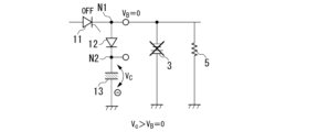
- 2A and 2B are diagrams illustrating the battery abnormality determination process of the battery charging device 1 according to the present embodiment.
- FIG. 2A shows an example in which the thyristor 11 is in an off state and the battery 3 is in a normal state.
- the capacitor 13 is charged with a voltage VC, and the voltage VC is expressed by the following equation (1).
- the load unit 5 indicates a load connected to the output line L1.
- FIG. 2B shows an example of an abnormal state in which the thyristor 11 is in an off state and the battery 3 is disconnected.
- the voltage at the node N2 becomes the voltage VC charged in the capacitor 13 when the thyristor 11 is turned on.
- the voltage VB of the node N1 is discharged through the load section 5 and becomes 0V. Therefore, the relationship between voltage VC and voltage VB is expressed by the following equation (2).
- the voltage VC of the capacitor 13 (the voltage at the node N2) becomes a voltage larger than the voltage VB.
- the switching control unit 14 uses the characteristics shown in FIGS. 2A and 2B described above to determine an abnormal state in which the battery 3 cannot be used, and when it is determined that the battery 3 is in an abnormal state, the set voltage is changed to the set voltage V1.
- a switching signal S1 is outputted to the voltage control section 17 to lower the voltage from the set voltage V2 to the set voltage V2.
- FIG. 3 is a flowchart showing an example of the operation of the battery charging device 1 according to this embodiment.
- the switching control unit 14 of the battery charging device 1 first determines whether the thyristor 11 is in the off period (step S101). The switching control unit 14 determines whether or not the thyristor 11 is in an off period, based on the control signal S2 of the thyristor 11, for example. When the thyristor 11 is in the off period (step S101: YES), the switching control unit 14 advances the process to step S102. Further, when the thyristor 11 is not in the off period (step S101: NO), the switching control unit 14 returns the process to step S101.
- step S102 the switching control unit 14 determines whether the voltage VC (the voltage at the node N2) is greater than the voltage VB (the voltage at the node N1).
- the switching control unit 14 advances the process to step S103.
- the switching control unit 14 advances the process to step S104.
- step S103 the switching control unit 14 switches the set voltage of the voltage control unit 17 to the lower set voltage V2. That is, the switching control unit 14 outputs a switching signal S1 for switching the set voltage to the set voltage V2 to the voltage control unit 17, and causes the voltage control unit 17 to switch the set voltage to the set voltage V2. After the process in step S103, the switching control unit 14 returns the process to step S101.
- step S104 the switching control unit 14 switches the set voltage of the voltage control unit 17 to the high set voltage V1. That is, the switching control unit 14 outputs a switching signal S1 for switching the set voltage to the set voltage V1 to the voltage control unit 17, and causes the voltage control unit 17 to switch the set voltage to the set voltage V1. After the process in step S104, the switching control unit 14 returns the process to step S101.
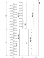
- FIG. 4 is a timing chart showing an example of the operation of the battery charging device 1 according to this embodiment.
- waveform W1 shows the waveform of the output voltage of generator 2
- waveform W2 shows the waveform of voltage VB (voltage at node N1).
- waveform W3 shows the waveform of switching signal S1
- waveform W4 shows the waveform of voltage VC (voltage of node N2).
- the horizontal axis of each waveform indicates time.
- a period TR1 indicates a period in which the battery 3 is in a normal state and is normally connected to the battery charging device 1.
- voltage VB has a substantially constant voltage waveform, as shown by waveform W2a.
- the switching control unit 14 since the voltage VC is smaller than the voltage VB, the switching control unit 14 outputs a switching signal S1 (for example, Low state) that switches the set voltage to the set voltage V1. do. Further, in this case, the voltage VC becomes a voltage as shown in the waveform W4a.
- period TR2 indicates a period of an abnormal state in which the battery 3 is disconnected.
- the voltage VB has a waveform like the waveform W2b, and becomes 0V during the off period TR3 of the thyristor 11.
- the switching control unit 14 sends a switching signal S1 (for example, Outputs a high state).
- the voltage VC is lower than the voltage of the waveform W4b in the period TR1, as shown in the waveform W4b.
- the off period TR3 of the thyristor 11 corresponds to a period in which the AC signal output from the generator 2 has a negative voltage.
- the voltage control unit 17 switches the set voltage to the set voltage V2 and performs control to output a voltage VC lower than that in the period TR1 (see waveform W4b).
- FIG. 5 is a diagram showing an example of the ripple current of the capacitor 13 of the battery charging device 1 according to this embodiment.
- waveform W5 shows the ripple current of capacitor 13 in battery charging device 1 of this embodiment when battery 3 is not connected.
- waveform W6 shows the ripple current of capacitor 13 when battery 3 is not connected and when the set voltage is left as set voltage V1. Waveform W6 corresponds to the ripple current of capacitor 13 in battery charging device 1 of the prior art.
- the ripple current of the capacitor 13 is reduced compared to the conventional technology (waveform W6) by lowering the set voltage to the set voltage V2. be able to.
- the battery charging device 1 includes the generator 2, the thyristor 11 (switching element), the diode 12, the capacitor 13, the voltage control section 17, and the switching control section 14. .
- the generator 2 generates power according to the rotation of the rotor, and outputs an alternating current signal according to the generated power.
- the thyristor 11 rectifies the AC signal output from the generator 2 and supplies it to the battery 3 as charging power.
- the diode 12 is connected between the output line L1 of the thyristor 11 and the FI load section 4 (load section), and supplies operating power to the FI load section 4.
- the capacitor 13 is connected to the output line L3 of the diode 12 and in parallel with the FI load section 4.
- the voltage control section 17 controls conduction of the thyristor 11 so that the voltage supplied to the FI load section 4 becomes the set voltage of the output target.
- the switching control unit 14 lowers the set voltage (for example, switches to the set voltage V2) when the battery 3 is in an abnormal state where it cannot be used.
- the battery charging device 1 according to the present embodiment supplies power to the FI load unit 4 side, for example, as shown in the waveform W5 shown in FIG.
- the current ripple current Irp can be reduced. Therefore, in the battery charging device 1 according to this embodiment, there is no need to increase the capacity of the capacitor 13. That is, the battery charging device 1 according to the present embodiment can reduce the ripple current Irp of the current supplied to the load section side (FI load section 4 side) without increasing the capacitance of the capacitor 13.
- the switching control unit 14 controls the switching control unit 14 when the voltage VC of the output line L3 of the diode 12 is higher than the voltage VB of the output line L1 of the thyristor 11 during the period when the thyristor 11 is in the off state (non-conducting state). It is determined that there is an abnormal state.
- the battery charging device 1 uses a simple method of comparing the voltage VC of the output line L3 and the voltage VB of the output line L1 during the period when the thyristor 11 is in the off state (non-conducting state). It can be easily determined that the battery 3 is in an abnormal state where it cannot be used.
- the switching control unit 14 determines whether or not the alternating current signal output by the generator 2 is in an abnormal state during a period when the voltage is negative.
- the battery charging device 1 can compare, for example, the voltage VC of the output line L3 and the voltage VB of the output line L1 during a period in which the AC signal output from the generator 2 is a negative voltage. , it is possible to easily determine that the battery 3 is in an abnormal state where it cannot be used.
- the switching control unit 14 sets the set voltage to the set voltage V1 (first set voltage) for charging the battery 3 in a normal state where the battery 3 can be used.
- the switching control unit 14 switches the set voltage to a set voltage V2 (second set voltage) that allows the FI load unit 4 to operate and is lower than the set voltage V1.
- the battery charging device 1 according to the present embodiment switches the set voltage of the voltage control unit 17 to the set voltage V2 that enables the operation of the FI load unit 4 and is lower than the set voltage V1, thereby increasing the ripple current Irp of the capacitor 13. can be reduced. Therefore, the battery charging device 1 according to the present embodiment can appropriately operate the FI load section 4 even in an abnormal state such as, for example, when the battery 3 is disconnected. That is, the battery charging device 1 according to the present embodiment can appropriately operate a vehicle (for example, a motorcycle) equipped with the battery charging device 1 even in an abnormal state in which the battery 3 is disconnected.
- a vehicle for example, a motorcycle
- the above-mentioned switching element is the thyristor 11 (silicon controlled commutator).
- the voltage control section 17 controls the conduction timing of the thyristor 11 so that the voltage VC supplied to the FI load section 4 becomes the set voltage.
- the battery charging device 1 uses the thyristor 11 (silicon-controlled commutator) as a switching element to appropriately rectify the AC signal output from the generator 2 with a simple configuration. can.
- thyristor 11 silicon-controlled commutator
- the abnormal state includes a state in which the battery 3 is disconnected from its own device (battery charging device 1).
- the battery charging device 1 according to the present embodiment does not increase the capacity of the capacitor 13 even when the battery 3 is in an abnormal state where it is disconnected from its own device (battery charging device 1).
- the load units such as the FI load unit 4 can be operated appropriately.
- the present invention is not limited to the above-described embodiments, and can be modified without departing from the spirit of the present invention.
- the switching element is the thyristor 11, but the switching element is not limited to this.
- other switching elements such as other silicon controlled commutators.
- the generator 2 is a single-phase magnetic AC generator, but the generator 2 is not limited to this, and can generate AC signals of multiple phases (for example, 3 phases). It may be a generator that outputs power, or it may be another generator.
- the processing of the switching control section 14 and the voltage control section 17 may be realized by software processing, or may be realized by hardware processing such as an electronic circuit. That is, the switching control section 14 and the voltage control section 17 may be realized by circuit means, or may be realized by software processing that causes a CPU (Central Processing Unit) to execute a program.
- a CPU Central Processing Unit
- the battery charging device 1 it is better to realize the processing of the switching control section 14 and the voltage control section 17 by hardware processing such as an electronic circuit, in order to prevent the occurrence of an abnormal state in which the battery 3 cannot operate normally. Therefore, the set voltage of the voltage control section 17 can be quickly switched. That is, the battery charging device 1 can quickly respond to the occurrence of an abnormal state.
- the switching control section 14 and the voltage control section 17 are realized with different configurations, but the present invention is not limited to this.
- a part of the switching control section 14 or All of them may be provided in the voltage control section 17.
- the switching control unit 14 determines whether the voltage VC of the output line L3 is larger than the voltage VB of the output line L1
- the voltage control unit 17 determines whether the voltage VC of the output line L1 is higher than the voltage VB of the output line L1
- An abnormal state such as connection of the battery 3 may be determined based on the determination result of whether the voltage is higher than the voltage VB.
- part or all of the functions of the switching control section 14 and the voltage control section 17 may be realized as an integrated circuit such as an LSI (Large Scale Integration).
- LSI Large Scale Integration
- Each of the above-mentioned functions may be implemented as an individual processor, or some or all of them may be integrated into a processor.
- the method of circuit integration is not limited to LSI, but may be realized using a dedicated circuit or a general-purpose processor. Further, if an integrated circuit technology that replaces LSI emerges due to advances in semiconductor technology, an integrated circuit based on this technology may be used.
Landscapes
- Engineering & Computer Science (AREA)
- Power Engineering (AREA)
- Control Of Charge By Means Of Generators (AREA)
Abstract
Description
本願は、2022年8月8日に、日本に出願された特願2022-126531号に基づき優先権を主張し、その内容をここに援用する。
図1は、本実施形態によるバッテリ充電装置1の一例を示すブロック図である。
図2A及び図2Bは、本実施形態によるバッテリ充電装置1のバッテリの異常判定処理を説明する図である。
図3は、本実施形態によるバッテリ充電装置1の動作の一例を示すフローチャートである。
図4は、本実施形態によるバッテリ充電装置1の動作の一例を示すタイミングチャートである。
図5は、本実施形態によるバッテリ充電装置1のコンデンサ13のリプル電流の一例を示す図である。
また、波形W5は、バッテリ3が接続されていない場合の本実施形態のバッテリ充電装置1におけるコンデンサ13のリプル電流を示している。また、波形W6は、比較のために、バッテリ3が接続されていない場合、且つ、設定電圧を設定電圧V1のままにした場合におけるコンデンサ13のリプル電流を示している。波形W6は、従来技術のバッテリ充電装置1におけるコンデンサ13のリプル電流に相当する。
これにより、本実施形態によるバッテリ充電装置1は、発電機2が出力する交流信号が負電圧の期間に、例えば、出力線L3の電圧VCと、出力線L1の電圧VBとを比較することで、バッテリ3が使用不可能な異常状態であることを簡単に判定することができる。
これにより、本実施形態によるバッテリ充電装置1は、バッテリ3が自装置(バッテリ充電装置1)との接続が外れた異常状態になった場合であっても、コンデンサ13の容量を増大させずに、FI負荷部4などの負荷部を適切に動作させることができる。
例えば、上記の実施形態において、スイッチング素子が、サイリスタ11である例を説明したが、これに限定されるものではなく、例えば、MOS(Metal-Oxide-Semiconductor)トランジスタ、IGBT(Insulated Gate Bipolar Transistor)、他のシリコン制御整流子などの他のスイッチング素子であってもよい。
2 発電機
3 バッテリ
4 FI負荷部
5 負荷部
10 レギュレータ
11 サイリスタ
12、15、16 ダイオード
13 コンデンサ
14 切替制御部
17 電圧制御部
Claims (6)
- 回転子の回転に応じて発電し、発電した電力に応じた交流信号を出力する発電機と、
前記発電機が出力する前記交流信号を整流して充電電力としてバッテリに供給するスイッチング素子と、
前記スイッチング素子の出力線と負荷部との間に接続され、前記負荷部に動作電力を供給するダイオードと、
前記ダイオードの出力線に接続され、且つ、前記負荷部と並列に接続されるコンデンサと、
前記負荷部に供給する電圧が、出力目標の設定電圧になるように、前記スイッチング素子の導通を制御する電圧制御部と、
前記バッテリが使用不可能な異常状態になった場合に、前記設定電圧を低下させる切替制御部と
を備えるバッテリ充電装置。 - 前記切替制御部は、前記スイッチング素子が非導通状態の期間において、前記ダイオードの出力線の電圧が、前記スイッチング素子の出力線の電圧より大きい場合に、前記異常状態であると判定する
請求項1に記載のバッテリ充電装置。 - 前記切替制御部は、前記交流信号が負電圧の期間に、前記異常状態であるか否かを判定する
請求項1に記載のバッテリ充電装置。 - 前記切替制御部は、
前記バッテリが使用可能な正常状態において、前記設定電圧を、前記バッテリを充電する第1設定電圧に設定し、
前記異常状態である場合に、前記設定電圧を、前記負荷部を動作可能で、前記第1設定電圧より低い第2設定電圧に切り替える
請求項1から請求項3のいずれか一項に記載のバッテリ充電装置。 - 前記スイッチング素子は、サイリスタであり、
前記電圧制御部は、
前記負荷部に供給する電圧が、前記設定電圧になるように、前記スイッチング素子の導通タイミングを制御する
請求項1から請求項3のいずれか一項に記載のバッテリ充電装置。 - 前記異常状態は、前記バッテリが自装置との接続が外れた状態を含む
請求項1から請求項3のいずれか一項に記載のバッテリ充電装置。
Priority Applications (1)
| Application Number | Priority Date | Filing Date | Title |
|---|---|---|---|
| JP2024540484A JP7734855B2 (ja) | 2022-08-08 | 2023-08-08 | バッテリ充電装置 |
Applications Claiming Priority (2)
| Application Number | Priority Date | Filing Date | Title |
|---|---|---|---|
| JP2022-126531 | 2022-08-08 | ||
| JP2022126531 | 2022-08-08 |
Publications (1)
| Publication Number | Publication Date |
|---|---|
| WO2024034602A1 true WO2024034602A1 (ja) | 2024-02-15 |
Family
ID=89851815
Family Applications (1)
| Application Number | Title | Priority Date | Filing Date |
|---|---|---|---|
| PCT/JP2023/028909 Ceased WO2024034602A1 (ja) | 2022-08-08 | 2023-08-08 | バッテリ充電装置 |
Country Status (2)
| Country | Link |
|---|---|
| JP (1) | JP7734855B2 (ja) |
| WO (1) | WO2024034602A1 (ja) |
Citations (3)
| Publication number | Priority date | Publication date | Assignee | Title |
|---|---|---|---|---|
| JP2011061950A (ja) * | 2009-09-09 | 2011-03-24 | Denso Corp | 電力変換装置 |
| JP2013020755A (ja) * | 2011-07-08 | 2013-01-31 | Shindengen Electric Mfg Co Ltd | 制御装置、及び制御方法 |
| WO2019163078A1 (ja) * | 2018-02-23 | 2019-08-29 | 新電元工業株式会社 | 車両用led点灯制御装置、及び、車両用led点灯制御装置の制御方法 |
-
2023
- 2023-08-08 JP JP2024540484A patent/JP7734855B2/ja active Active
- 2023-08-08 WO PCT/JP2023/028909 patent/WO2024034602A1/ja not_active Ceased
Patent Citations (3)
| Publication number | Priority date | Publication date | Assignee | Title |
|---|---|---|---|---|
| JP2011061950A (ja) * | 2009-09-09 | 2011-03-24 | Denso Corp | 電力変換装置 |
| JP2013020755A (ja) * | 2011-07-08 | 2013-01-31 | Shindengen Electric Mfg Co Ltd | 制御装置、及び制御方法 |
| WO2019163078A1 (ja) * | 2018-02-23 | 2019-08-29 | 新電元工業株式会社 | 車両用led点灯制御装置、及び、車両用led点灯制御装置の制御方法 |
Also Published As
| Publication number | Publication date |
|---|---|
| JPWO2024034602A1 (ja) | 2024-02-15 |
| JP7734855B2 (ja) | 2025-09-05 |
Similar Documents
| Publication | Publication Date | Title |
|---|---|---|
| EP0777309B1 (en) | Generating apparatus for vehicle | |
| EP0464694A2 (en) | Power source unit for an automotive vehicle | |
| JPH0624432B2 (ja) | 電界効果トランジスタを利用する電気装置 | |
| JPH04325839A (ja) | 車両用電源装置 | |
| EP3790156A1 (en) | A multi-input power converter, a controlling method thereof and an uninterrupted power supply including the same | |
| US12301051B2 (en) | Power device terminal backup switch unit | |
| JP7734855B2 (ja) | バッテリ充電装置 | |
| JPH07337021A (ja) | 直流−交流変換装置 | |
| JPWO2018084309A1 (ja) | 排ガスエネルギー回収装置 | |
| JP2025168261A (ja) | バイク用の発電システム及び方法 | |
| JP7621140B2 (ja) | 電源装置、及び電源制御方法 | |
| JP7446133B2 (ja) | バッテリ充電装置、及び電流制御装置 | |
| WO2022121659A1 (zh) | 充电装置及充电系统 | |
| JP7450771B2 (ja) | バッテリ充電装置、及び電流制御装置 | |
| CN106464181B (zh) | 电力转换装置 | |
| WO2020222261A1 (en) | A system and a method for protecting a regulator rectifier device and a respective protection device | |
| WO2024128215A1 (ja) | バッテリ充電装置、制御装置、及び保護方法 | |
| WO2023275934A1 (ja) | バッテリ充電装置、及び電流制御装置 | |
| WO2024024934A1 (ja) | バッテリ充電装置 | |
| JPS62250876A (ja) | 電圧形インバ−タ装置 | |
| US20240405578A1 (en) | Power supply device, control device, and control method | |
| KR0123466Y1 (ko) | 차량용 배터리의 충전 제어회로 | |
| CN100386940C (zh) | 电力系统 | |
| CN121238967A (zh) | 供电电路、桥臂驱动电路、功率单元、功率模块及其控制方法、控制装置和制冷设备 | |
| SU540335A1 (ru) | Бесконтактный регул тор напр жени дл автомобильных генераторов |
Legal Events
| Date | Code | Title | Description |
|---|---|---|---|
| 121 | Ep: the epo has been informed by wipo that ep was designated in this application |
Ref document number: 23852564 Country of ref document: EP Kind code of ref document: A1 |
|
| WWE | Wipo information: entry into national phase |
Ref document number: 2024540484 Country of ref document: JP |
|
| WWE | Wipo information: entry into national phase |
Ref document number: 202517008969 Country of ref document: IN |
|
| WWP | Wipo information: published in national office |
Ref document number: 202517008969 Country of ref document: IN |
|
| NENP | Non-entry into the national phase |
Ref country code: DE |
|
| 122 | Ep: pct application non-entry in european phase |
Ref document number: 23852564 Country of ref document: EP Kind code of ref document: A1 |