WO2024034191A1 - スイッチング電源回路、及び、スイッチング電源回路を備える電子装置 - Google Patents
スイッチング電源回路、及び、スイッチング電源回路を備える電子装置 Download PDFInfo
- Publication number
- WO2024034191A1 WO2024034191A1 PCT/JP2023/015819 JP2023015819W WO2024034191A1 WO 2024034191 A1 WO2024034191 A1 WO 2024034191A1 JP 2023015819 W JP2023015819 W JP 2023015819W WO 2024034191 A1 WO2024034191 A1 WO 2024034191A1
- Authority
- WO
- WIPO (PCT)
- Prior art keywords
- power supply
- supply circuit
- weighting coefficient
- voltage
- output voltage
- Prior art date
- Legal status (The legal status is an assumption and is not a legal conclusion. Google has not performed a legal analysis and makes no representation as to the accuracy of the status listed.)
- Ceased
Links
Images





Classifications
-
- H—ELECTRICITY
- H02—GENERATION; CONVERSION OR DISTRIBUTION OF ELECTRIC POWER
- H02M—APPARATUS FOR CONVERSION BETWEEN AC AND AC, BETWEEN AC AND DC, OR BETWEEN DC AND DC, AND FOR USE WITH MAINS OR SIMILAR POWER SUPPLY SYSTEMS; CONVERSION OF DC OR AC INPUT POWER INTO SURGE OUTPUT POWER; CONTROL OR REGULATION THEREOF
- H02M3/00—Conversion of DC power input into DC power output
- H02M3/22—Conversion of DC power input into DC power output with intermediate conversion into AC
- H02M3/24—Conversion of DC power input into DC power output with intermediate conversion into AC by static converters
- H02M3/28—Conversion of DC power input into DC power output with intermediate conversion into AC by static converters using discharge tubes with control electrode or semiconductor devices with control electrode to produce the intermediate AC
- H02M3/325—Conversion of DC power input into DC power output with intermediate conversion into AC by static converters using discharge tubes with control electrode or semiconductor devices with control electrode to produce the intermediate AC using devices of a triode or a transistor type requiring continuous application of a control signal
- H02M3/335—Conversion of DC power input into DC power output with intermediate conversion into AC by static converters using discharge tubes with control electrode or semiconductor devices with control electrode to produce the intermediate AC using devices of a triode or a transistor type requiring continuous application of a control signal using semiconductor devices only
- H02M3/3353—Conversion of DC power input into DC power output with intermediate conversion into AC by static converters using discharge tubes with control electrode or semiconductor devices with control electrode to produce the intermediate AC using devices of a triode or a transistor type requiring continuous application of a control signal using semiconductor devices only having at least two simultaneously operating switches on the input side, e.g. "double forward" or "double (switched) flyback" converter
-
- H—ELECTRICITY
- H02—GENERATION; CONVERSION OR DISTRIBUTION OF ELECTRIC POWER
- H02M—APPARATUS FOR CONVERSION BETWEEN AC AND AC, BETWEEN AC AND DC, OR BETWEEN DC AND DC, AND FOR USE WITH MAINS OR SIMILAR POWER SUPPLY SYSTEMS; CONVERSION OF DC OR AC INPUT POWER INTO SURGE OUTPUT POWER; CONTROL OR REGULATION THEREOF
- H02M1/00—Details of apparatus for conversion
- H02M1/44—Circuits or arrangements for compensating for electromagnetic interference in converters or inverters
-
- H—ELECTRICITY
- H02—GENERATION; CONVERSION OR DISTRIBUTION OF ELECTRIC POWER
- H02M—APPARATUS FOR CONVERSION BETWEEN AC AND AC, BETWEEN AC AND DC, OR BETWEEN DC AND DC, AND FOR USE WITH MAINS OR SIMILAR POWER SUPPLY SYSTEMS; CONVERSION OF DC OR AC INPUT POWER INTO SURGE OUTPUT POWER; CONTROL OR REGULATION THEREOF
- H02M3/00—Conversion of DC power input into DC power output
- H02M3/22—Conversion of DC power input into DC power output with intermediate conversion into AC
- H02M3/24—Conversion of DC power input into DC power output with intermediate conversion into AC by static converters
- H02M3/28—Conversion of DC power input into DC power output with intermediate conversion into AC by static converters using discharge tubes with control electrode or semiconductor devices with control electrode to produce the intermediate AC
- H02M3/325—Conversion of DC power input into DC power output with intermediate conversion into AC by static converters using discharge tubes with control electrode or semiconductor devices with control electrode to produce the intermediate AC using devices of a triode or a transistor type requiring continuous application of a control signal
- H02M3/335—Conversion of DC power input into DC power output with intermediate conversion into AC by static converters using discharge tubes with control electrode or semiconductor devices with control electrode to produce the intermediate AC using devices of a triode or a transistor type requiring continuous application of a control signal using semiconductor devices only
- H02M3/33507—Conversion of DC power input into DC power output with intermediate conversion into AC by static converters using discharge tubes with control electrode or semiconductor devices with control electrode to produce the intermediate AC using devices of a triode or a transistor type requiring continuous application of a control signal using semiconductor devices only with automatic control of the output voltage or current, e.g. flyback converters
-
- Y—GENERAL TAGGING OF NEW TECHNOLOGICAL DEVELOPMENTS; GENERAL TAGGING OF CROSS-SECTIONAL TECHNOLOGIES SPANNING OVER SEVERAL SECTIONS OF THE IPC; TECHNICAL SUBJECTS COVERED BY FORMER USPC CROSS-REFERENCE ART COLLECTIONS [XRACs] AND DIGESTS
- Y02—TECHNOLOGIES OR APPLICATIONS FOR MITIGATION OR ADAPTATION AGAINST CLIMATE CHANGE
- Y02B—CLIMATE CHANGE MITIGATION TECHNOLOGIES RELATED TO BUILDINGS, e.g. HOUSING, HOUSE APPLIANCES OR RELATED END-USER APPLICATIONS
- Y02B70/00—Technologies for an efficient end-user side electric power management and consumption
- Y02B70/10—Technologies improving the efficiency by using switched-mode power supplies [SMPS], i.e. efficient power electronics conversion e.g. power factor correction or reduction of losses in power supplies or efficient standby modes
Definitions
- the present disclosure relates to a switching power supply circuit, and particularly relates to a technique effective for reducing the amount of radiated radio noise emitted from a switching power supply circuit.
- power supply circuits For example, in order to reduce the burden on the environment, switching power supply circuits with high power efficiency are increasingly being adopted as power supply circuits.
- electronic devices including power supply circuits include electronic devices in vehicles such as automobiles, control devices in industrial equipment, and electronic devices, but are not limited to these devices.
- Switching power supply circuits have higher power efficiency than linear regulator (dropper) power supply circuits.
- the switching power supply circuit generates radiated electromagnetic noise due to the switching timing between the rise and fall of the pulse signal used in the switching power supply circuit.
- radiated electromagnetic noise increases in high frequency bands.
- Patent Document 1 discloses a switching power supply circuit that can improve PSRR (power supply voltage fluctuation rejection ratio). Specifically, the technique of Patent Document 1 sets the sampling timing of the A/D converter to an arbitrary position on the slope of the ripple of the output voltage. As a result, even if the input voltage fluctuates and the amount of ripple in the output voltage changes, the center of the ripple in the output voltage is stabilized at the reference voltage according to the target value, making it possible to improve PSRR. It is disclosed that this will happen.
- PSRR power supply voltage fluctuation rejection ratio
- One of the objectives is to provide a switching power supply circuit capable of reducing the amount of radiated electromagnetic noise even due to changes in the load or set voltage of the switching power supply circuit, and an electronic device equipped with the switching power supply circuit. There is a particular thing. Other objects and novel features will become apparent from the description of this specification and the accompanying drawings.
- a typical switching power supply circuit includes a pulse width control section that controls the pulse width of the pulse voltage output from the switching transistor, and a drive voltage control section that controls the drive voltage that determines the magnitude of the pulse voltage output from the switching transistor. and the difference value between the output voltage setting value set in advance for the power supply circuit and the output voltage measurement value that is the measurement result of the output voltage of the power supply circuit, and the weight for the pulse width based on the output voltage setting value. It includes a weighting coefficient calculation unit that determines a weighting coefficient and a weighting coefficient for the drive voltage.
- FIG. 1 is a block diagram showing an example of the overall configuration of a switching power supply circuit using PWM control as a comparative example.
- A is a schematic diagram of a pulse waveform when the pulse width applied to the gate of the switching transistor of the switching power supply circuit of FIG. 1 is wide (pulse duty ratio is large).
- B is a diagram schematically showing a waveform induced to the secondary side when the pulse waveform of (A) is applied to the primary side of the transformer.
- C) is a diagram showing an example of the output voltage of the switching power supply circuit after the waveform in (B) passes through a low-pass filter.
- D is a schematic diagram of a pulse waveform when the pulse width applied to the gate of the switching transistor of the switching power supply circuit of FIG.
- FIG. 1 is narrow (pulse duty ratio is small).
- E is a diagram schematically showing a waveform induced to the secondary side when the pulse waveform of (D) is applied to the primary side of the transformer.
- F is a diagram showing an example of the output voltage of the switching power supply circuit after the waveform of (E) passes through a low-pass filter.
- FIG. 3 is a block diagram showing an example of the overall configuration of the switching power supply circuit according to this embodiment.
- (A) is a diagram showing the change in the weighting coefficient K p calculated by the weighting coefficient calculation unit of the switching power supply circuit according to the present embodiment in FIG. 3 by the slope of the curve CP1.
- FIG. 5 is an image diagram schematically showing changes in the weighting coefficient K p and changes in the weighting coefficient K v .
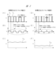
- (A) shows an example of a pulse applied to the gate of the switching transistor of the switching power supply circuit according to the comparative example in FIG. 1 and the switching power supply circuit according to the present embodiment in FIG. 3 to generate the same output voltage.
- FIG. 3 is a diagram comparing waveforms of an example of pulses applied to the gates of switching transistors in FIG. (B) is a diagram comparing the frequency characteristics of electromagnetic radiation noise generated by the waveforms in (A).
- FIG. 8 is a diagram illustrating an example of a weighting coefficient calculating section of a switching power supply circuit according to the present embodiment and a modification of the present embodiment.
- FIG. 9 is a diagram illustrating another example of the weighting coefficient calculation section of the switching power supply circuit according to the present embodiment and a modification of the present embodiment.
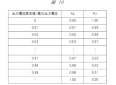
- FIG. 10 is a diagram showing an example of a case where weighting coefficients of a switching power supply circuit according to a modification of the present embodiment are provided as a lookup table.
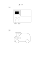
- A is a schematic diagram showing an example of an industrial device in which a switching power supply circuit according to the present embodiment and a modification of the present embodiment is incorporated.
- B is a schematic diagram showing an example of a vehicle in which a switching power supply circuit according to the present embodiment and a modification of the present embodiment is incorporated.
- the constituent elements are not necessarily essential, unless explicitly stated or when they are considered to be clearly essential in principle. Needless to say.
- shape, positional relationship, etc. of components, etc. when referring to the shape, positional relationship, etc. of components, etc., the shape, positional relationship, etc. of components, etc. are referred to, unless specifically stated or when it is considered that it is clearly not possible in principle. This shall include things that approximate or are similar to, etc. This also applies to the above numerical values and ranges.
- circuit elements constituting each functional block of the embodiments are not particularly limited, but may be formed on a semiconductor substrate such as single crystal silicon by known integrated circuit technology such as CMOS (complementary MOS transistor). Alternatively, it is formed on a circuit board on which electronic components such as ICs are combined and mounted.
- CMOS complementary MOS transistor
- FIG. 1 is a block diagram showing an example of the overall configuration of a switching power supply circuit 70 using PWM control.
- the switching power supply circuit 70 includes an input voltage source V 1 , switching transistors SWp and SWn, a transformer Tr1, a rectifier circuit section 10, a low-pass filter section 20, an output voltage measurement section 30, an output voltage setting section 40, a difference calculation section 50, and a pulse width.
- a control section 60 is provided. Since the basic operation of a switching power supply circuit using PWM control is a conventional technique, a detailed explanation will be omitted and the explanation will focus on the part related to this embodiment.
- the input voltage source V1 outputs a constant voltage value Vc .
- the output voltage measurement unit 30 measures the voltage value of the output voltage V out output from the low-pass filter unit 20.
- the difference calculation unit 50 calculates a difference voltage value that is the difference between the value of the output voltage V out and the target voltage value set by the output voltage setting unit 40, and determines how far the current output voltage value is from the target voltage value. Calculate whether there is a deviation.
- Pulse width control section 60 controls the pulse widths of switching transistors SWp and SWn based on the differential voltage value.
- the pulse width control section 60 sets the pulse widths of the switching transistors SWp and SWn to be wide. Further, when the differential voltage value is large and the current output voltage value exceeds the target voltage value, the pulse width control section 60 sets the pulse widths of the switching transistors SWp and SWn narrowly.
- a secondary voltage V tr is generated on the secondary side of the transformer Tr1, which is induced by the pulse voltage on the primary side of the transformer Tr1.
- a secondary voltage V tr is generated on the secondary side of the transformer Tr1, which is induced by the pulse voltage on the primary side of the transformer Tr1.
- FIG. 2A, 2B, and 2C show that in the PWM-controlled switching power supply circuit 70 of FIG. 1, the pulse widths of the pulses (V p , V n ) applied to the gates of the switching transistors SWp and SWn are 7 is a graph showing the operation when the output voltage is relatively large.
- the ON state of the switching transistors SWp and SWn is longer than the OFF state, that is, the pulse width applied to the gate of the switching transistor is large, and the duty ratio is large (the duty ratio is greater than 0.25). ) indicates the condition.
- FIG. 2(B) shows a change in the secondary voltage V tr induced on the secondary side of the transformer Tr1 by the pulse of FIG. 2(A).
- the switching transistor SWp When the switching transistor SWp is in the ON state, a pulse is generated on the positive side of the midpoint voltage. Furthermore, when the switching transistor SWn is in the ON state, a pulse is generated on the negative side of the midpoint voltage.
- An example of the switching frequency is several kilohertz to several hundred kilohertz.
- the pulse width is wide, the high frequency components of the radiated electromagnetic noise generated at the rise and fall of the secondary voltage V tr are relatively small.
- FIG. 2C shows the voltage value of the output voltage V out output from the low-pass filter section 20, and shows how high frequency components are reduced by the low-pass filter section 20.
- the ON state of the switching transistors SWp and SWn is shorter than the OFF state, that is, the pulse width applied to the gate of the switching transistor is narrow, and the duty ratio is small (the duty ratio is less than 0.5). ) indicates the condition.
- FIG. 2(E) shows a change in the secondary voltage V tr induced on the secondary side of the transformer Tr1 by the pulse of FIG. 2(D).
- a pulse with a narrow pulse width is generated on the positive side of the midpoint voltage.
- a pulse with a narrow pulse width is generated on the negative side of the midpoint voltage.
- An example of the switching frequency is several kilohertz to several hundred kilohertz.
- the pulse width is narrow, the high frequency components of the radiated electromagnetic noise generated at the rise and fall of the secondary voltage V tr become relatively large.
- the output voltage of the input voltage source V1 is a constant voltage value Vc , so the duty ratio of the switching transistor becomes small, and the radiated electromagnetic noise increases.
- the frequency component becomes large. That is, the smaller the duty ratio, the more impulse-like pulses are generated, and the higher frequency components of the radiated electromagnetic noise tend to become larger.
- FIG. 2F shows the voltage value of the output voltage V out output from the low-pass filter section 20, and shows how high frequency components are reduced by the low-pass filter section 20.
- FIG. 3 is a block diagram showing an example of the overall configuration of a switching power supply circuit 1000 according to this embodiment.
- the switching power supply circuit 1000 includes an input voltage source V 200 (variable output), switching transistors SWp100 and SWn100, a transformer Tr100, a rectifier circuit section 800, a low-pass filter section 700, an output voltage measurement section 500, an output voltage setting section 600, and a difference calculation section. 400, a weighting coefficient calculation section 300, a drive voltage control section 200, and a pulse width control section 100.
- the pulse width control section 100 controls the duty ratio of the switching transistors SWp100 and SWn100.
- the duty ratio has a duty ratio lower limit value DML, and the pulse width control section 100 never sets a duty ratio lower than the duty ratio lower limit value DML.
- the duty ratio lower limit value DML can be determined by the frequency of the radiated electromagnetic noise and the intensity of the radiated electromagnetic noise. For example, it is possible to set the duty ratio lower limit value DML so that the frequency of the radiated electromagnetic noise and the intensity of the radiated electromagnetic noise fall within a range that complies with domestic and international standards that define radiated electromagnetic noise.
- the duty ratio lower limit value DML can be set to 0.2, that is, the duty ratio ratio corresponding to the duty ratio lower limit value DML can be set to 20%.
- the VCCI Voluntary Control Council for Interference by Information Technology Equipment
- examples of foreign standards include standards by the FCC (Federal Communications Commission) and CE (European Conformity) in Europe. Note that it is also possible to set the value of the duty ratio lower limit value DML and the ratio of the duty ratio corresponding to the duty ratio lower limit value DML to arbitrary values.
- the drive voltage control unit 200 can be controlled to change the drive voltage Vd , which is the output voltage of the input voltage source V200 . Since the conventional switching power supply circuit did not include the drive voltage control section 200 according to this embodiment, even if the output voltage value of the switching power supply circuit becomes small, the output voltage value of the input voltage source outputs a constant value. Was. Therefore, a case may occur in which the pulse width control unit 60 controls the duty ratio to be lower than the duty ratio lower limit value DML, and the radiated electromagnetic noise moves from the low frequency band to the high frequency band, and the level of the radiated electromagnetic noise In some cases, a situation may occur in which the amount of data becomes large.
- the weighting coefficient calculation unit 300 has a function of calculating a weighting coefficient Kp for the duty ratio controlled by the pulse width control unit 100 and a weighting coefficient Kv for the drive voltage Vd controlled by the drive voltage control unit 200.
- the weighting coefficient Kp and the weighting coefficient Kv can change nonlinearly with respect to fluctuations in the output voltage V out of the switching power supply circuit 1000.
- a case will be described in detail where the weighting coefficient Kp and the weighting coefficient Kv change non-linearly with respect to fluctuations in the output voltage V out of the switching power supply circuit 1000. It is also possible to have a configuration that changes linearly with respect to .
- the weighting coefficient calculation unit 300 is capable of calculating a weighting coefficient Kp. Conversely, when the output voltage V out increases, the weighting coefficient Kv for the drive voltage V d becomes smaller, and when the output voltage V out decreases, the weighting coefficient Kv for the drive voltage V d decreases. The weighting coefficient calculation unit 300 can calculate the weighting coefficient Kv so that the weighting coefficient Kv becomes larger.
- the output voltage V out decreases by the weighting coefficient calculation unit 300 calculating the weighting coefficient Kp and the weighting coefficient Kv, the output voltage V out is controlled by the drive voltage V d.
- the difference calculation unit 400 compares the voltage value of the output voltage V out measured by the output voltage measurement unit 500 and the set voltage value set by the output voltage setting unit 600, and calculates the voltage value of the output voltage V out and the corresponding voltage value. Calculates difference information from the set voltage value.
- the difference information may be an analog voltage value expressed by an analog signal, or may be a digital voltage value expressed by a digital signal.
- the output voltage measuring section 500 has a function of measuring the voltage value of the output voltage V out of the switching power supply circuit 1000. Since the configuration of the output voltage measuring section 500 is a known technique, detailed explanation will be omitted.
- the output voltage setting unit 600 has a function of outputting a set voltage value set as the output voltage V out of the switching power supply circuit 1000.
- the set voltage value is input to the difference calculation section 400 and the weighting coefficient calculation section 300.
- the set voltage value information indicating the set voltage value may be an analog set voltage value expressed by an analog signal, or may be a digital voltage value expressed by a digital signal.
- the input voltage source V 200 is configured to be able to change the driving voltage V d , which is the output voltage of the input voltage source V 200 , by the driving voltage controller 200. That is, the driving voltage V d of the input voltage source V 200 is a variable output.
- FIG. 4A is a diagram showing an example of the duty ratio control operation of the pulse width control section 100 when the output voltage of the switching power supply circuit 1000 according to the present embodiment is varied or when the load is varied.
- a straight line JP1 shown as a comparative example shows an example of a duty ratio control operation of a conventional switching power supply circuit using only PWM control.
- the duty ratio decreases while the voltage of the input voltage source remains high.
- radiated electromagnetic noise occurs in the high frequency band, and the radiated The level of electromagnetic noise becomes high.
- the pulse width control unit 100 of the switching power supply circuit 1000 controls the duty ratio according to the curve CP1 so as not to fall into the region R1 (do not control the output voltage in the region R1).
- the duty ratio is set large.
- the pulse width control unit 100 controls the duty ratio so that the duty ratio asymptotically approaches the duty ratio lower limit value DML.
- the slope of the curve CP1 corresponds to the weighting coefficient Kp of the duty ratio determined by the weighting coefficient calculating section 300.
- FIG. 4A it can be seen that as the output voltage V out increases by ⁇ V, the slope of the curve CP1 increases, and the weighting coefficient Kp of the duty ratio also increases.
- FIG. 4(B) is a diagram showing an example of the control operation of the drive voltage control section 200 when the output voltage of the switching power supply circuit 1000 according to the present embodiment is varied or when the load is varied.
- a straight line JV1 shown as a comparative example is a graph showing the power supply voltage applied to switching transistors SWp and SWn of a conventional switching power supply circuit using only PWM control.
- the conventional switching power supply circuit did not include the drive voltage control section 200 according to the present embodiment, so even when the output voltage value of the switching power supply circuit becomes small, the output voltage value of the input voltage source remains unchanged. was outputting a constant value. That is, on the straight line JV1, the same voltage is applied to the switching transistors SWp and SWn regardless of the output voltage value of the switching power supply circuit.
- the drive voltage control unit 200 of the switching power supply circuit 1000 controls the drive voltage V d , which is the output voltage value of the input voltage source V 200 , using the curve CV1.
- the drive voltage V d which is the output voltage value of the input voltage source V 200
- the drive voltage control unit 200 is set close to the maximum value. Output voltage.
- the drive voltage V d which is the output voltage value of the input voltage source V 200
- the slope of the curve CV1 corresponds to the weighting coefficient Kv of the drive voltage Vd , which is determined by the weighting coefficient calculating section 300.
- FIG. 4B it can be seen that as the output voltage V out increases by ⁇ V, the slope of the curve CV1 decreases, and the weighting coefficient Kv of the drive voltage V d also decreases.
- the switching power supply circuit 1000 when the duty ratio asymptotically approaches the duty ratio lower limit value DML, the ratio of output voltage control by the duty ratio decreases (weighting coefficient Kp (becomes smaller), and the ratio of output voltage control by the drive voltage Vd increases (the weighting coefficient Kv becomes larger). Furthermore, in the switching power supply circuit 1000, when the duty ratio becomes larger than the lower limit value DML of the duty ratio, the proportion of output voltage control by the duty ratio increases (the weighting coefficient Kp increases), and the output voltage control by the drive voltage V d increases. The ratio decreases (the weighting coefficient Kv decreases).
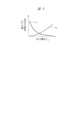
- FIG. 5 is an image diagram schematically showing a change in the weighting coefficient K p and a change in the weighting coefficient K v with respect to a change in the output voltage V out .
- the weighting coefficient Kp increases nonlinearly, and the weighting coefficient Kv decreases nonlinearly.
- the value of the output voltage V out corresponding to the intersection of the curve drawn by the weighting coefficient Kp and the curve drawn by the weighting coefficient Kv can be set to an arbitrary value.
- FIG. 6(A) shows an example of a pulse (vj1) applied to the gate of the switching transistor of the switching power supply circuit according to the comparative example of FIG. 1 to generate the same output voltage
- FIG. 3 is a diagram comparing waveforms of an example of a pulse (vm1) applied to the gate of a switching transistor in a switching power supply circuit according to the present invention.
- the pulse vj1 according to the comparative example has a duty ratio of 5% and an amplitude of 5 volts.
- the pulse vm1 according to the present embodiment has a duty ratio of 25% and an amplitude of 1 volt.
- Pulse vj1 and pulse vm1 are input-side pulses that are formed in order to generate an output voltage of approximately 0.25 volts.
- the ratio of the duty ratio lower limit value DML is set to 20%, instead of setting the duty ratio ratio to 25% to generate a low output voltage, the voltage value of the pulse vm1 is lowered. ing.
- the pulse vm1 shows an example; for example, the duty ratio of the pulse vm1 can be set to a value exceeding 25%, and the amplitude value of the pulse vm1 can be set to less than 1 volt. In this case, it is expected that the frequency band of the electromagnetic radiation noise caused by the pulse vm1 will further decrease, and the level of the electromagnetic radiation noise will further decrease.
- FIG. 6(B) is a diagram comparing the frequency characteristics of electromagnetic radiation noise generated by the waveforms of FIG. 6(A).
- the electromagnetic radiation noise f vj1 caused by the pulse vj1 is the third harmonic of the electromagnetic radiation noise of the pulse vj1.
- the electromagnetic radiation noise fvm1 caused by the pulse vm1 is the third harmonic of the electromagnetic radiation noise of the pulse vm1.
- the electromagnetic radiation noise f vm1 is also smaller ⁇ fd3 than the electromagnetic radiation noise f vj1 , and the electromagnetic radiation noise of the switching power supply circuit according to the present embodiment is different from that of the switching power supply circuit that executes only PWM control according to the comparative example.
- electromagnetic radiation of the switching power supply circuit according to this embodiment also occurs in the nth harmonic (n is an odd number) such as the fifth harmonic and the seventh harmonic. It can be seen that the noise is smaller than the electromagnetic radiation noise of the switching power supply circuit that executes only PWM control according to the comparative example.
- the switching power supply circuit according to the present embodiment described above it is possible to provide a switching power supply circuit that can reduce the amount of radiated electromagnetic noise in a high frequency band even due to changes in load or set voltage, etc. become. That is, according to the switching power supply circuit according to the present embodiment, it is possible to reduce noise components around the transformer when outputting a low voltage, and to suppress electromagnetic radiation noise. Furthermore, even if the hardware of an electronic device that uses the switching power supply circuit according to this embodiment is updated and the load or voltage value to be controlled changes, electromagnetic radiation noise can be suppressed and the electronic device can be This makes it possible to reduce the effects of
- FIGS. 7A and 7B show the weighting coefficient Kp for the duty ratio controlled by the pulse width control unit 100 of the switching power supply circuit according to a modification of the present embodiment, and the drive controlled by the drive voltage control unit 200.
- FIG. 7 is a diagram showing another example of a weighting coefficient Kv for voltage Vd .
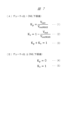
- FIG. 7A shows the relationship between the weighting coefficient Kp and the weighting coefficient Kv when the duty ratio exceeds the duty ratio lower limit value DML.
- the weighting coefficient Kp for the duty ratio is determined by formula (1), where the output voltage setting value of the switching power supply circuit is V out and the maximum output voltage value is V outmax . ). That is, the weighting coefficient Kp is a value obtained by dividing the output voltage setting value of the switching power supply circuit by the maximum output voltage value.
- the weighting coefficient Kv is expressed by equation (2) obtained by subtracting the weighting coefficient Kp from 1. As is clear from equations (1) and (2), when the weighting coefficient Kv and the weighting coefficient Kp are added together, they become 1 as shown in equation (3).
- FIG. 7B shows the relationship between the weighting coefficient Kp and the weighting coefficient Kv when the duty ratio is equal to or less than the duty ratio lower limit value DML.
- the weighting coefficient Kp for the duty ratio is calculated as shown in equation (4). Fixed to "0". That is, when the duty ratio as a calculation result is equal to or less than the duty ratio lower limit value DML, the switching power supply circuit according to this modification does not perform PWM control.
- the weighting coefficient Kv for the drive voltage Vd controlled by the drive voltage control unit 200 when the duty ratio is less than or equal to the duty ratio lower limit value DML is fixed to "1" as shown in equation (5). That is, when the duty ratio as a calculation result is equal to or less than the duty ratio lower limit value DML, the switching power supply circuit according to the present modification controls the output voltage using the drive voltage.
- the weighting coefficient Kp when the duty ratio as a calculation result becomes equal to or less than the duty ratio lower limit value DML due to changes in the load or set voltage, the weighting coefficient Kp is changed.
- the weighting coefficient Kv is fixed to "0" and the weighting coefficient Kv is fixed to "1".
- FIG. 8 is a circuit diagram of a weighting coefficient calculating section 300_1 configured by mainly using analog circuits.
- Operational amplifier AKp calculates a weighting coefficient Kp using input resistance Ri and variable resistance Rfp.
- the Kp control unit 310_1 that controls the weighting coefficient Kp inputs the differential voltage V df output from the difference calculation unit 400 and the set voltage V st output from the output voltage setting unit 600 shown in FIG.
- the weighting coefficient Kp is multiplied by the differential voltage V df , the multiplication result is inverted by the inverting amplifier Ikp, and the calculation result is output to the pulse width control section 100 as a pulse width control value.
- operational amplifier AKv calculates a weighting coefficient Kv using input resistance Ri and variable resistance Rfv.
- the Kv control unit 320_1 that controls the weighting coefficient Kv inputs the differential voltage V df output from the difference calculation unit 400 and the set voltage V st output from the output voltage setting unit 600 shown in FIG.
- the weighting coefficient Kv is multiplied by the differential voltage V df , the multiplication result is inverted by the inverting amplifier Ikv, and the calculation result is output to the drive voltage control section 200 as a drive voltage control value.
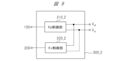
- FIG. 9 is a circuit diagram of a weighting coefficient calculation unit 300_2 in which the weighting coefficient calculation unit 300 is mainly composed of digital circuits.
- the Kp control unit 310_2 calculates a weighting coefficient Kp by inputting the differential voltage V df output from the difference calculation unit 400 shown in FIG. 3 and the set voltage V st output from the output voltage setting unit 600. Then, the weighting coefficient Kp is multiplied by the differential voltage V df , and the calculation result is output to the pulse width control section 100 as a pulse width control value.
- the Kv control unit 320_2 calculates a weighting coefficient Kv by inputting the differential voltage V df output from the difference calculation unit 400 shown in FIG. 3 and the set voltage V st output from the output voltage setting unit 600. Then, the weighting coefficient Kv is multiplied by the differential voltage V df , and the calculation result is output to the drive voltage control section 200 as a drive voltage control value.
- FIG. 10 is a lookup table of weighting coefficients Kp and weighting coefficients Kv that can be used by the weighting coefficient calculation unit 300_1 and/or the weighting coefficient calculation unit 300_2.
- the lookup table can be stored in a storage unit (not shown) provided in the weighting coefficient calculation unit 300_1 and/or the weighting coefficient calculation unit 300_2. Further, the lookup table can also be stored in a storage unit (not shown) provided outside the weighting coefficient calculation unit 300_1 and/or the weighting coefficient calculation unit 300_2.
- the lookup table of weighting coefficient Kp and weighting coefficient Kv shown in FIG. 10 is the result of calculation using the formula shown in FIG. Therefore, the weighting coefficient calculation unit 300_1 and/or the weighting coefficient calculation unit 300_2 calculates the weighting coefficient Kp and the weighting coefficient Kv using the formulas shown in FIG. 7 without using the lookup table shown in FIG. It is also possible.
- FIGS. 11(A) and 11(B) are schematic diagrams showing an example in which a switching power supply circuit according to this embodiment or a modification of this embodiment is mounted on various electronic devices.
- the electronic device is not limited to the electronic device shown in FIGS. 11(A) and 11(B), and can be equipped with a switching power supply circuit according to this embodiment or a modification of this embodiment. means all electronic devices.
- FIG. 11(A) is an example of an industrial device equipped with a switching power supply circuit 1000.
- a load that uses the output voltage of the switching power supply circuit 1000 or a control circuit that uses the output voltage as a control voltage is shown as 2001.
- FIG. 11(B) is an example of a vehicle equipped with a switching power supply circuit 1000.
- the ECU installed in a vehicle may be updated, and as described above, the switching power supply circuit 1000 is configured to be able to respond to the update.
- a load that uses the output voltage of the switching power supply circuit 1000 or a control circuit that uses the output voltage as a control voltage is shown as 2002.
- the switching power supply circuit in the fields of mobility and industrial equipment, it is possible to guarantee stable operation of a system including electronic equipment even after a partial hardware update for long-term use and long-term operation.
- the switching power supply circuit according to the present embodiment provides a switching power supply circuit that can reduce the amount of radiated electromagnetic noise in the high frequency band even due to changes in load or set voltage. It becomes possible to provide.
- switching power supply circuit has been described as a center-tap type
- the switching power supply circuits of the present embodiment and modifications are not limited to the center-tap type.
- the technology of this embodiment and modifications can be applied to ringing choke type, flyback type, forward type, half bridge type, full bridge type, non-isolated step-down type, step-up type, and resonant type switching power supply circuits. It is also possible to do so.
- Pulse width control section 200 Drive voltage control section 300, 300_1, 300_2 Weighting coefficient calculation section 400 Difference calculation section 500 Output voltage measurement section 600 Output voltage setting section 700 Low pass filter section 800 Rectification circuit section Tr100 Transformer SWp100, SWn100 Switching transistor V 200 input voltage source
Landscapes
- Engineering & Computer Science (AREA)
- Power Engineering (AREA)
- Physics & Mathematics (AREA)
- Electromagnetism (AREA)
- Dc-Dc Converters (AREA)
Abstract
Description
図3は本実施形態に係るスイッチング電源回路1000の全体構成の一例を示すブロック図である。スイッチング電源回路1000は、入力電圧源V200(可変出力)、スイッチングトランジスタSWp100、SWn100、トランスTr100、整流回路部800、ローパスフィルタ部700、出力電圧測定部500、出力電圧設定部600、差分演算部400、重みづけ係数演算部300、駆動電圧制御部200、及び、パルス幅制御部100を備える。
図6(A)は、同一の出力電圧を生成するために、図1の比較例に係るスイッチング電源回路のスイッチングトランジスタのゲートに印加されるパルスの一例(vj1)と、図3の本実施形態に係るスイッチング電源回路のスイッチングトランジスタのゲートに印加されるパルスの一例(vm1)の波形を比較した図である。
図7(A)及び(B)は、本実施形態の変形例に係るスイッチング電源回路のパルス幅制御部100が制御するデューティ比に対する重みづけ係数Kp、及び、駆動電圧制御部200が制御する駆動電圧Vdに対する重みづけ係数Kvの他の一例を示す図である。
200 駆動電圧制御部
300、300_1、300_2 重みづけ係数演算部
400 差分演算部
500 出力電圧測定部
600 出力電圧設定部
700 ローパスフィルタ部
800 整流回路部
Tr100 トランス
SWp100、SWn100 スイッチングトランジスタ
V200 入力電圧源
Claims (7)
- スイッチングトランジスタから出力されるパルス電圧のパルス幅を制御するパルス幅制御部と、
前記スイッチングトランジスタから出力される前記パルス電圧の大きさを決定する駆動電圧を制御する駆動電圧制御部と、
電源回路に対してあらかじめ設定された出力電圧設定値と前記電源回路の出力電圧の測定結果である出力電圧測定値との差分値、及び、前記出力電圧設定値に基づいて、前記パルス幅に対する重みづけ係数、及び、前記駆動電圧に対する重みづけ係数を決定する重みづけ係数演算部と、を備えるスイッチング電源回路。 - 前記重みづけ係数演算部によって、
前記パルス幅に対する重みづけ係数は、前記出力電圧測定値が増加すると大きくなり、前記出力電圧測定値が減少すると小さくなるように演算され、
前記駆動電圧に対する重みづけ係数は、前記出力電圧測定値が増加すると小さくなり、前記出力電圧測定値が減少すると大きくなるように演算され、
さらに、前記パルス幅に対する重みづけ係数は、前記パルス電圧のデューティ比があらかじめ定められたデューティ比を下回らないように演算される請求項1に記載のスイッチング電源回路。 - 前記パルス幅に対する重みづけ係数、及び、前記駆動電圧に対する重みづけ係数は正の値であり、
前記パルス幅に対する重みづけ係数と、前記駆動電圧に対する重みづけ係数を加算演算した値が1となる請求項1に記載のスイッチング電源回路。 - 前記パルス幅に対する重みづけ係数は、前記出力電圧設定値を前記電源回路の最大出力電圧値で除算した値であり、
前記駆動電圧に対する重みづけ係数は、1から前記パルス幅に対する重みづけ係数を減算した値である請求項3に記載のスイッチング電源回路。 - 前記パルス電圧のデューティ比があらかじめ定められたデューティ比を下回る場合には、前記パルス幅に対する重みづけ係数を0とし、前記駆動電圧に対する重みづけ係数を1とし、
前記パルス幅制御部は、前記パルス電圧のデューティ比をあらかじめ定められたデューティ比に固定するように制御する請求項4に記載のスイッチング電源回路。 - 前記スイッチングトランジスタを一次側に備え、二次側に整流回路、及び、ローパスフィルタ回路を備えるトランスをさらに含む請求項1に記載のスイッチング電源回路。
- 請求項1乃至6のいずれか一項に記載のスイッチング電源回路と、
前記電源回路によって供給される出力電圧を制御電圧とする制御回路と、を含む電子装置。
Priority Applications (1)
| Application Number | Priority Date | Filing Date | Title |
|---|---|---|---|
| US18/859,740 US20250266769A1 (en) | 2022-08-12 | 2023-04-20 | Switching Power Supply Circuit and Electronic Device Including Switching Power Supply Circuit |
Applications Claiming Priority (2)
| Application Number | Priority Date | Filing Date | Title |
|---|---|---|---|
| JP2022-128853 | 2022-08-12 | ||
| JP2022128853A JP2024025424A (ja) | 2022-08-12 | 2022-08-12 | スイッチング電源回路、及び、スイッチング電源回路を備える電子装置 |
Publications (1)
| Publication Number | Publication Date |
|---|---|
| WO2024034191A1 true WO2024034191A1 (ja) | 2024-02-15 |
Family
ID=89851463
Family Applications (1)
| Application Number | Title | Priority Date | Filing Date |
|---|---|---|---|
| PCT/JP2023/015819 Ceased WO2024034191A1 (ja) | 2022-08-12 | 2023-04-20 | スイッチング電源回路、及び、スイッチング電源回路を備える電子装置 |
Country Status (3)
| Country | Link |
|---|---|
| US (1) | US20250266769A1 (ja) |
| JP (1) | JP2024025424A (ja) |
| WO (1) | WO2024034191A1 (ja) |
Citations (4)
| Publication number | Priority date | Publication date | Assignee | Title |
|---|---|---|---|---|
| JPH11187662A (ja) * | 1997-12-24 | 1999-07-09 | Isuzu Motors Ltd | Dc−dcコンバータ |
| JP2000102249A (ja) * | 1998-09-22 | 2000-04-07 | Fuji Xerox Co Ltd | 高圧電源装置 |
| JP2014168342A (ja) * | 2013-02-28 | 2014-09-11 | Ricoh Co Ltd | スイッチングレギュレータ |
| JP2020089079A (ja) * | 2018-11-26 | 2020-06-04 | 株式会社ベルニクス | プッシュプル電圧共振型コンバータ回路 |
Family Cites Families (1)
| Publication number | Priority date | Publication date | Assignee | Title |
|---|---|---|---|---|
| JP5298872B2 (ja) * | 2009-01-19 | 2013-09-25 | 株式会社デンソー | Pwm制御装置 |
-
2022
- 2022-08-12 JP JP2022128853A patent/JP2024025424A/ja active Pending
-
2023
- 2023-04-20 WO PCT/JP2023/015819 patent/WO2024034191A1/ja not_active Ceased
- 2023-04-20 US US18/859,740 patent/US20250266769A1/en active Pending
Patent Citations (4)
| Publication number | Priority date | Publication date | Assignee | Title |
|---|---|---|---|---|
| JPH11187662A (ja) * | 1997-12-24 | 1999-07-09 | Isuzu Motors Ltd | Dc−dcコンバータ |
| JP2000102249A (ja) * | 1998-09-22 | 2000-04-07 | Fuji Xerox Co Ltd | 高圧電源装置 |
| JP2014168342A (ja) * | 2013-02-28 | 2014-09-11 | Ricoh Co Ltd | スイッチングレギュレータ |
| JP2020089079A (ja) * | 2018-11-26 | 2020-06-04 | 株式会社ベルニクス | プッシュプル電圧共振型コンバータ回路 |
Also Published As
| Publication number | Publication date |
|---|---|
| US20250266769A1 (en) | 2025-08-21 |
| JP2024025424A (ja) | 2024-02-26 |
Similar Documents
| Publication | Publication Date | Title |
|---|---|---|
| US8928303B2 (en) | Apparatus and methods for transient compensation of switching power regulators | |
| US7589509B2 (en) | Switching regulator | |
| JP5481926B2 (ja) | 電源制御装置、電源装置、及び電源制御方法 | |
| US20050007167A1 (en) | PWM switching regulator control circuit | |
| US10020729B2 (en) | Current-mode DC/DC converter and method therefor | |
| US9331573B2 (en) | Circuit and method for controlling a switching transistor of a switching regulator | |
| US7545129B2 (en) | Switching power supply circuit | |
| US10320292B2 (en) | Phase compensation circuit and DC/DC converter using the same | |
| Yan et al. | An automotive-use battery-to-load GaN-based switching power converter with anti-aliasing MR-SSM and in-cycle adaptive ZVS techniques | |
| US12493312B2 (en) | Low-dropout regulator with noise cancellation and operation method thereof | |
| JP2006033958A (ja) | スイッチングレギュレータ | |
| JP2004078332A (ja) | スイッチングレギュレータ及びスロープ補正回路 | |
| JP5977738B2 (ja) | スイッチング電源装置及びこれを用いた電子機器 | |
| US11750078B2 (en) | Adaptive off-time or on-time DC-DC converter | |
| US20040113597A1 (en) | DC-DC converter and DC-DC converter drive circuit | |
| KR20230069827A (ko) | Dcdc 컨버터의 작동 전압 범위를 확장하기 위한 적응형 최소 듀티 사이클 설계 | |
| US9755510B2 (en) | Switching power supply | |
| CN110391735B (zh) | 具有可编程脉冲跳频模式的pwm模式升压开关调节器 | |
| WO2024034191A1 (ja) | スイッチング電源回路、及び、スイッチング電源回路を備える電子装置 | |
| US20200343814A1 (en) | Switching power supply | |
| US11424685B2 (en) | Resonance type power supply device | |
| US7135843B2 (en) | Switching power supply device | |
| JP4370128B2 (ja) | Dc−dcコンバータ | |
| US20090066309A1 (en) | Switching regulator | |
| US11557968B2 (en) | Power supply circuit capable of stable operation |
Legal Events
| Date | Code | Title | Description |
|---|---|---|---|
| 121 | Ep: the epo has been informed by wipo that ep was designated in this application |
Ref document number: 23852177 Country of ref document: EP Kind code of ref document: A1 |
|
| WWE | Wipo information: entry into national phase |
Ref document number: 18859740 Country of ref document: US |
|
| NENP | Non-entry into the national phase |
Ref country code: DE |
|
| 122 | Ep: pct application non-entry in european phase |
Ref document number: 23852177 Country of ref document: EP Kind code of ref document: A1 |
|
| WWP | Wipo information: published in national office |
Ref document number: 18859740 Country of ref document: US |