WO2024034166A1 - 光学装置 - Google Patents
光学装置 Download PDFInfo
- Publication number
- WO2024034166A1 WO2024034166A1 PCT/JP2023/007579 JP2023007579W WO2024034166A1 WO 2024034166 A1 WO2024034166 A1 WO 2024034166A1 JP 2023007579 W JP2023007579 W JP 2023007579W WO 2024034166 A1 WO2024034166 A1 WO 2024034166A1
- Authority
- WO
- WIPO (PCT)
- Prior art keywords
- prism
- light
- light source
- wavelength
- functional layer
- Prior art date
- Legal status (The legal status is an assumption and is not a legal conclusion. Google has not performed a legal analysis and makes no representation as to the accuracy of the status listed.)
- Ceased
Links
Images



Classifications
-
- G—PHYSICS
- G02—OPTICS
- G02B—OPTICAL ELEMENTS, SYSTEMS OR APPARATUS
- G02B27/00—Optical systems or apparatus not provided for by any of the groups G02B1/00 - G02B26/00, G02B30/00
- G02B27/18—Optical systems or apparatus not provided for by any of the groups G02B1/00 - G02B26/00, G02B30/00 for optical projection, e.g. combination of mirror and condenser and objective
-
- G—PHYSICS
- G02—OPTICS
- G02B—OPTICAL ELEMENTS, SYSTEMS OR APPARATUS
- G02B5/00—Optical elements other than lenses
- G02B5/04—Prisms
-
- H—ELECTRICITY
- H01—ELECTRIC ELEMENTS
- H01S—DEVICES USING THE PROCESS OF LIGHT AMPLIFICATION BY STIMULATED EMISSION OF RADIATION [LASER] TO AMPLIFY OR GENERATE LIGHT; DEVICES USING STIMULATED EMISSION OF ELECTROMAGNETIC RADIATION IN WAVE RANGES OTHER THAN OPTICAL
- H01S5/00—Semiconductor lasers
- H01S5/02—Structural details or components not essential to laser action
- H01S5/022—Mountings; Housings
- H01S5/0225—Out-coupling of light
- H01S5/02253—Out-coupling of light using lenses
-
- H—ELECTRICITY
- H01—ELECTRIC ELEMENTS
- H01S—DEVICES USING THE PROCESS OF LIGHT AMPLIFICATION BY STIMULATED EMISSION OF RADIATION [LASER] TO AMPLIFY OR GENERATE LIGHT; DEVICES USING STIMULATED EMISSION OF ELECTROMAGNETIC RADIATION IN WAVE RANGES OTHER THAN OPTICAL
- H01S5/00—Semiconductor lasers
- H01S5/02—Structural details or components not essential to laser action
- H01S5/022—Mountings; Housings
- H01S5/0225—Out-coupling of light
- H01S5/02255—Out-coupling of light using beam deflecting elements
Definitions
- the present disclosure relates to an optical device.
- the projector which is an optical device described in Patent Document 1
- the image exposure device which is an optical device described in Patent Document 2
- An optical device includes a first surface, a second surface forming an angle of 45 degrees with the first surface, and a second surface forming an angle of 45 degrees with the second surface and 90 degrees with the first surface.
- a first prism having a third surface forming an angle of 45 degrees, a fourth surface bonded to the second surface of the first prism, and a fifth surface forming an angle of 45 degrees with the fourth surface;
- a second prism having a sixth surface forming an angle of 45 degrees with the fifth surface and forming an angle of 90 degrees with the fourth surface; a first light source that emits light of a first wavelength; and a first light source having a first wavelength.
- a second light source that emits light of a second wavelength different from the first prism; and a second light source that is provided along the second surface of the first prism to reflect the light of the first wavelength and transmit the light of the second wavelength.
- a first optical functional layer that reflects light from the first light source, and a second optical functional layer that is provided along the sixth surface of the second prism and reflects light of the second wavelength.
- the light from the second light source is The light enters the fifth surface of the prism, is reflected by the second optical functional layer, passes through the first optical functional layer, exits from the first surface of the first prism, and is reflected by the second optical functional layer.
- a condensing lens is arranged on an extension of the optical axis of light emitted from one surface, and the wavelength of the light from one of the first light source and the second light source is shorter than the wavelength of the light from the other, and the refractive index is and the first light source and the second light source are arranged such that the optical path length from one of the first light source and the second light source to the condensing lens is shorter than the optical path length from the other to the condensing lens. It is characterized by having been.
- the above optical device can suppress the increase in size of the light emitting part.
- FIG. 3 is a front view of the optical device.
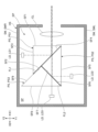
- FIG. 3 is a cross-sectional view of the optical device.
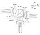
- FIG. 3 is a perspective view of a prism and a light source.
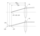
- FIG. 3 is a diagram schematically showing the relationship between the positions of three light sources with respect to a condenser lens and the spread of light emitted by the three light sources.
- FIG. 3 is a diagram showing how light emitted from a light source passes through a prism and reaches a condensing lens.
- FIG. 3 is a top view of a light emitting section provided within the housing.
- FIG. 1 is a front view of the optical device 100
- FIG. 2 is a cross-sectional view of the optical device 100.
- FIG. 2 shows a cross section of the optical device 100 on a virtual plane parallel to the XY plane represented by the dashed line LN1 in FIG.
- FIG. 3 is a perspective view of the light source LD and prism PS that constitute the light emitting section EP of the optical device 100.
- X1 represents one direction of the X-axis constituting the three-dimensional orthogonal coordinate system
- X2 represents the other direction of the X-axis
- Y1 represents one direction of the Y-axis constituting the three-dimensional orthogonal coordinate system
- Y2 represents the other direction of the Y-axis
- Z1 represents one direction of the Z axis constituting the three-dimensional orthogonal coordinate system
- Z2 represents the other direction of the Z axis.
- the X1 side of the optical device 100 corresponds to the front side (front side) of the optical device 100
- the X2 side of the optical device 100 corresponds to the rear side (back side) of the optical device 100.
- the Y1 side of the optical device 100 corresponds to the left side of the optical device 100
- the Y2 side of the optical device 100 corresponds to the right side of the optical device 100
- the Z1 side of the optical device 100 corresponds to the upper side of the optical device 100
- the Z2 side of the optical device 100 corresponds to the lower side of the optical device 100. The same applies to other figures.
- the optical device 100 is a device that includes a light source LD and a prism PS.
- the optical device 100 is a color sensor that discriminates the color of a subject, and as shown in FIG. It includes a light-emitting part EP and a light-receiving part RP that are housed in a housing space SP inside.
- the housing HS includes a pair of side walls SW (a left wall SWL and a right wall SWR) facing each other along the width direction (Y-axis direction) perpendicular to the depth direction (X-axis direction). , and a housing space SP formed between a pair of side walls SW (left side wall SWL and right side wall SWR).
- the optical device 100 applies the light emitted by the light emitting part EP to the subject, receives the light reflected by the subject by the light receiving part RP, and calculates the intensity based on the intensity of each wavelength of the light received by the light receiving part RP. , is configured to determine whether the color of the subject is the same as a predetermined color.
- the light receiving unit RP may be configured to receive light transmitted through the subject.
- the light receiving section RP is provided below the light emitting section EP (Z2 side) in the housing HS, and includes a light receiving lens LS and a light receiving element PD, as shown in FIG.
- the light receiving lens LS is configured to have a maximum diameter that fits within the width (value WD) of the housing HS. This is to improve color discrimination performance by increasing the amount of received light as much as possible.
- the light emitting unit EP includes three light sources LD (first light source LD1, second light source LD2, and third light source LD3) and three prisms PS (first prism PS1, second prism PS2, and It is configured to include a third prism PS3) and a condensing lens CL.
- the light source LD is configured to emit light of a specific color.
- each of the three light sources LD (first light source LD1, second light source LD2, and third light source LD3) is composed of a single wavelength laser diode.
- Single-wavelength laser diodes are preferred over light-emitting diodes in that they can emit light in a narrower wavelength range than light-emitting diodes and therefore do not require an achromatic lens.
- at least one of the three light sources LD may be composed of a light emitting diode.
- the first light source LD1 is a single wavelength laser diode that emits light of a first wavelength
- the second light source LD2 is a single wavelength laser diode that emits light of a second wavelength different from the first wavelength
- the third light source LD3 is a single wavelength laser diode that emits light of a third wavelength different from both the first wavelength and the second wavelength.
- the first wavelength light is blue light from 430 nm to 490 nm
- the second wavelength light is red light from 640 nm to 770 nm
- the third wavelength light is green light from 490 nm to 550 nm.
- blue light is represented by a dash-dotted line
- red light is represented by a dash-double-dotted line
- green light is represented by a thick dotted line. The same applies to FIGS. 4 to 6, which will be described later.
- each of the three light sources LD is mounted on a board (not shown) and fixed to the housing HS via the board.
- the prism PS is an optical element for dispersing, refracting, total internal reflection, or birefringence of light.
- the prism PS is a dichroic prism formed of a transparent medium such as glass or crystal, and is fixed to the housing HS.
- each of the three prisms PS (first prism PS1, second prism PS2, and third prism PS3) is formed of glass and has the same shape (triangular prism shape) and have the same size.
- the first prism PS1 has a first surface SF1 facing the condenser lens CL, a second surface SF2 forming an angle of 45 degrees with the first surface SF1, and a second surface SF2 forming an angle of 45 degrees with the second surface SF2.
- the first surface SF1 forms an angle of 90 degrees
- the third surface SF3 forms an angle of 90 degrees.
- the third surface SF3 of the first prism PS1 is a surface facing the first light source LD1, and is arranged parallel to and opposite to the inner surface of the right side wall SWR of the housing HS.
- the second prism PS2 has a fourth surface SF4 bonded to the second surface SF2 of the first prism PS1, a fifth surface SF5 forming an angle of 45 degrees with the fourth surface SF4, and a fifth surface SF5. It has a sixth surface SF6 that forms an angle of 45 degrees with the fifth surface SF5 and an angle of 90 degrees with the fourth surface SF4.
- the fifth surface SF5 of the second prism PS2 is a surface facing the second light source LD2, and is arranged to face the inner surface of the left side wall SWL of the housing HS in parallel.
- the third prism PS3 has a seventh surface SF7 bonded to the sixth surface SF6 of the second prism PS2, an eighth surface SF8 forming an angle of 45 degrees with the seventh surface SF7, and an eighth surface SF8 that forms an angle of 45 degrees with the seventh surface SF7. It has a ninth surface SF9 that forms an angle of 45 degrees with the eight surface SF8 and an angle of 90 degrees with the seventh surface SF7.
- the eighth surface SF8 of the third prism PS3 is a surface facing the third light source LD3, and is arranged to face the inner surface of the rear wall of the housing HS in parallel.
- the first optical functional layer FL1 is provided along the second surface SF2 of the first prism PS1.
- the first optical functional layer FL1 is a layer that reflects light of a first wavelength and transmits light of wavelengths other than the first wavelength.
- the first optical functional layer FL1 is provided along the second surface SF2 of the first prism PS1 between the second surface SF2 of the first prism PS1 and the fourth surface SF4 of the second prism PS2.
- the first optical functional layer FL1 may be coated on the fourth surface of the second prism PS2.
- the first optical functional layer FL1 is provided along the entire second surface SF2 of the first prism PS1, but a part of the second surface SF2 of the first prism PS1 (light source LD It may also be provided along the area (portion exposed to light).
- the second optical functional layer FL2 is provided along the sixth surface SF6 of the second prism PS2.
- the second optical functional layer FL2 is a layer that reflects light of a second wavelength and transmits light of a wavelength other than the second wavelength.
- the second optical functional layer FL2 is provided along the sixth surface SF6 of the second prism PS2 between the sixth surface SF6 of the second prism PS2 and the seventh surface SF7 of the third prism PS3.
- the second optical functional layer FL2 may be coated on the seventh surface of the third prism PS3.
- the second optical functional layer FL2 is provided along the entire surface of the sixth surface SF6 of the second prism PS2, but a part of the sixth surface SF6 of the second prism PS2 (light source LD It may also be provided along the area (portion exposed to light).
- each of the three prisms PS is bonded to each other with an adhesive.
- each of the three prisms PS may be joined without using an adhesive.
- the light emitting unit EP of the optical device 100 is configured to include three light sources LD and three prisms PS, but the third light source LD3 and the third prism PS3 may be omitted. .
- the condensing lens CL is an optical element used to direct the light emitted by the light source LD in a desired direction.
- the condenser lens CL is a lens used to direct the light emitted by each of the first light source LD1, second light source LD2, and third light source LD3 in a desired direction, and the prism PS ( It is arranged on the downstream side of the first surface SF1) of the first prism PS1.
- FIG. 4 is a diagram schematically showing the relationship between the relative positions of the three light sources LD with respect to the condenser lens CL and the spread of light emitted by the three light sources LD. Specifically, the upper diagram in FIG.
- FIG. 4 shows the distance (optical path length) between the first light source LD1 and the condensing lens CL, the distance (optical path length) between the second light source LD2 and the condensing lens CL, 4 is a diagram when the distances (optical path lengths) between the third light source LD3 and the condenser lens CL are the same, and the lower diagram in FIG. 4 is a diagram when the three distances (optical path lengths) are different from each other.
- FIG. 4 shows the distance (optical path length) between the first light source LD1 and the condensing lens CL, the distance (optical path length) between the second light source LD2 and the condensing lens CL, 4 is a diagram when the distances (optical path lengths) between the third light source LD3 and the condenser lens CL are the same, and the lower diagram in FIG. 4 is a diagram when the three distances (optical path lengths) are different from each other.
- FIG. 4 shows the distance (optical path
- the uppermost optical path of the blue light emitted by the first light source LD1 is represented by a dashed-dotted line
- the uppermost optical path of the red light emitted by the second light source LD2 is represented by a dashed-dot line
- the uppermost optical path of the green light emitted from the third light source LD3 is represented by a thick dotted line.
- illustration of the three prisms PS located between each of the three light sources LD and the condenser lens CL is omitted.
- the first light source LD1 emits blue light.
- the green light emitted by the third light source LD3 is spread out more than the blue light
- the red light emitted by the second light source LD2 is spread out more than the green light.
- the optical path length DS2 is larger than the optical path length DS3
- the optical path length DS3 is larger than the optical path length DS1.
- the optical device 100 can emit three lights (blue light, red light, and green light) emitted from the three light sources LD when each of the optical path lengths DS1, DS2, and DS3 are appropriately set. It is possible to make the spread of the light the same when each of the lights (light) exits one common condensing lens CL.
- FIG. 5 is a diagram showing how light emitted from the light source LD passes through the prism PS and reaches the condenser lens CL.
- the upper diagram in FIG. 5 shows how the blue light emitted by the first light source LD1 passes through the first prism PS1 and reaches the condenser lens CL
- the lower diagram in FIG. The figure shows how the emitted red light passes through the second prism PS2 and the first prism PS1 and reaches the condenser lens CL.
- FIG. 6 is a top view of the light emitting section EP provided within the housing HS.
- the left diagram in FIG. 6 is a top view of the light emitting unit EP described with reference to FIGS. 2 and 3, and the right diagram in FIG. It is a top view of part EPA.
- the light emitting unit EPA is mainly configured such that the first light source LD1 emits red light and the second light source LD2 emits blue light.
- the first light source LD1 emits blue light and the second light source LD2 emits red light. This is different from the light emitting section EP which emits the light.
- the letter "B" attached to the first light source LD1 indicates that the first light source LD1 emits blue light
- the letter "R” attached to the second light source LD2 indicates that the first light source LD1 emits blue light
- the letter "G” attached to the third light source LD3 represents that the third light source LD3 emits green light.
- the letter "R” attached to the first light source LD1 indicates that the first light source LD1 emits red light
- the letter "B” attached to the second light source LD2 indicates that the first light source LD1 emits red light.
- the letter "G” attached to the third light source LD3 represents that the third light source LD3 emits green light.
- a light source LD, a prism PS, and a condensing lens CL are arranged at the center. This is to make the width of the housing HS as small as possible.
- the optical axis OA means the optical axis of three lights emitted from each of the three light sources LD. Therefore, in the present embodiment, the light emitted by the first light source LD1 is reflected by the first optical functional layer FL1, and the light emitted by the second light source LD2 is reflected by the second optical functional layer FL2. is also located on the optical axis of the light emitted by the third light source LD3.
- the optical device 100 including the light emitting part EP is arranged such that the width of the housing HS is a value WD1, that is, the width of the optical axis OA and the left side wall of the housing HS are The distance between the outer surface of the SWL and the distance between the optical axis OA and the outer surface of the right side wall SWR of the housing HS are both configured to be the value WD1/2 (half of the value WD1). .
- the optical device 100 including the light emitting part EPA is configured such that the width of the housing HS is a value WD2, that is, the optical axis OA and the outer surface of the left side wall SWL of the housing HS. and the distance between the optical axis OA and the outer surface of the right side wall SWR of the housing HS are both configured to have a value WD2/2 (half of the value WD2).
- the width of the housing HS is the larger of the optical path length DS11 and the optical path length DS12. This is because it has to be more than twice as large as the average.
- the optical path length DS1, the optical path length DS2, and the optical path length DS3 should be adjusted appropriately. Since they need to be different, it is difficult to make the optical path length DS11, which is a part of the optical path length DS1, and the optical path length DS12, which is a part of the optical path length DS2, the same size.
- the first light source LD1 and the second light source LD2 are arranged so that the difference between the optical path length DS11 and the optical path length DS12 is as small as possible.
- the first light source LD1 emits blue light toward the first prism PS1, and the second light source LD2 emits red light toward the second prism PS2.
- the third light source LD3 is configured to emit green light toward the third prism PS3.
- the first light source LD1 emits red light toward the first prism PS1, the second light source LD2 emits blue light toward the second prism PS2, and the third light source LD3 emits green light toward the third prism PS3.
- the width of the housing HS (the difference between the optical path length DS11 and the optical path length DS12) can be made smaller than in the case where the light emitting part EPA is configured to emit light toward the light emitting part EPA.
- the distance (optical path length DS11) between the first light source LD1 and the optical axis OA (first optical functional layer FL1) in the light emitting part EP is It is larger than the distance (optical path length DS12) between the second light source LD2 and the optical axis OA (second optical functional layer FL2) in EP.
- the distance (optical path length DS11A) between the first light source LD1 and the optical axis OA (first optical functional layer FL1) in the light emitting part EPA is It is larger than the distance (optical path length DS12A) between the light source LD2 and the optical axis OA (second optical functional layer FL2).
- the optical path length DS11 in the light emitting unit EP in the left diagram of FIG. 6 is smaller than the optical path length DS11A in the light emitting unit EPA in the right diagram in FIG. DS12 is larger than the optical path length DS12A in the light emitting unit EPA in the right diagram of FIG. 6 by a distance difference DF2.
- the optical device 100 including the light emitting part EP has an optical path length DS12 smaller than the optical path length DS11, which is larger than the optical path length DS12A in the light emitting part EPA by the distance difference DF2, but an optical path length DS11 larger than the optical path length DS12. becomes smaller than the optical path length DS11A in the light emitting part EPA by the distance difference DF1.
- What is effective in reducing the width of the housing HS is to make the larger of the optical path length DS11 and the optical path length DS12 as small as possible.
- the optical device 100 including the light emitting part EP compared to the optical device 100 including the light emitting part EPA, it is possible to reduce the distance between the optical axis OA and the outer surface of the right side wall SWR of the housing HS by the distance difference DF3.
- the distance between the optical axis OA and the outer surface of the left side wall SWL of the housing HS can be reduced by the distance difference DF4.
- the distance difference DF3 and the distance difference DF4 are the same.
- the optical device 100 has a first surface SF1, a second surface SF2 forming an angle of 45 degrees with the first surface SF1, and a second surface SF2, as shown in FIG. a first prism PS1 having a third surface SF3 forming an angle of 45 degrees with the surface SF2 and an angle of 90 degrees with the first surface SF1; and a fourth surface SF4 bonded to the second surface SF2 of the first prism PS1.
- a fifth surface SF5 forming an angle of 45 degrees with the fourth surface SF4
- a sixth surface SF6 forming an angle of 45 degrees with the fifth surface SF5 and 90 degrees with the fourth surface SF4.
- a prism PS2 a first light source LD1 that emits light of a first wavelength, a second light source LD2 that emits light of a second wavelength different from the first wavelength, and a second light source LD2 that emits light of a second wavelength different from the first wavelength.
- a first optical functional layer FL1 is provided along the sixth surface SF6 of the second prism PS2 and is provided along the sixth surface SF6 of the second prism PS2 to reflect light of the first wavelength and transmit light of the second wavelength. 2nd optical function layer FL2 which reflects.
- the light from the first light source LD1 enters the third surface SF3 of the first prism PS1, is reflected by the first optical functional layer FL1, and exits from the first surface SF1 of the first prism PS1.
- the light from the second light source LD2 enters the fifth surface SF5 of the second prism PS2, is reflected by the second optical functional layer FL2, passes through the first optical functional layer FL1, and is transmitted to the fifth surface SF5 of the first prism PS1.
- the light is emitted from one surface SF1.
- a condenser lens CL is arranged on an extension of the optical axis of light emitted from the first surface SF1 of the first prism PS1.
- the wavelength of the light from one of the first light source LD1 and the second light source LD2 is shorter and has a higher refractive index than the wavelength of the light from the other.
- the first light source LD1 and the second light source LD2 are arranged so that the optical path length from one of the first light source LD1 and the second light source LD2 to the condensing lens CL is shorter than the optical path length from the other to the condensing lens CL.
- a light source LD2 is arranged.
- the first light source LD1 and a second light source LD2 are arranged.
- This configuration has the effect of suppressing chromatic aberration of the light emitted from the light emitting portion EP. This is because the spread of light (diameter of parallel light) can be made the same when each of the plurality of colors of light emitted by the plurality of light sources LD exits one common condensing lens CL. Furthermore, this configuration can suppress the chromatic aberration of the light emitted from the light emitting part EP, and therefore has the effect that an achromatic lens for suppressing the chromatic aberration can be omitted. Further, this configuration has the effect of suppressing an increase in the size of the light emitting section and an increase in the number of parts. This is because, in this configuration, a condenser lens is not disposed between each of the plurality of light sources LD and the prism PS, and an achromatic lens is also not disposed.
- first light source LD1 and the second light source LD2 may be single wavelength laser diodes.
- This configuration has the effect of being able to narrow the wavelength range of the emitted light from each of the first light source LD1 and the second light source LD2, and suppressing chromatic aberration, compared to the case where other light sources such as light emitting diodes are used. .
- the optical device 100 includes a pair of side walls SW (left side wall
- the housing HS may include a housing space SP formed between a pair of side walls SW (left side wall SWL and right side wall SWR) and a pair of side walls SW (left side wall SWL and right side wall SWR).
- the two prisms PS2 and the second light source LD2 may be sequentially arranged along the width direction (Y-axis direction).
- the first light source LD1 and the second light source LD2 may be configured such that the wavelength of the light from the first light source LD1 is shorter than the wavelength from the second light source LD2 and the refractive index is higher. good.
- the first optical path length (optical path length DS1) from the first light source LD1 to the condensing lens CL is shorter than the second optical path length (optical path length DS2) from the second light source LD2 to the condensing lens CL.
- FIG. see FIG. 2 may be arranged outside (on the Y1 side).
- the example shown in the left diagram of FIG. 6 is configured such that the second light source LD2 emits red light, and the first light source LD1 emits blue light that has a shorter wavelength and a higher refractive index than the red light. has been done.
- the first light source LD1 is arranged outside the third surface SF3 (see FIG. 2) of the first prism PS1 (on the Y2 side) so that the optical path length DS1 of the blue light is shorter than the optical path length DS2 of the red light.
- the second light source LD2 is arranged outside (Y1 side) of the fifth surface SF5 (see FIG. 2) of the second prism PS2. This configuration is as shown in the right side of FIG.
- the first light source LD1 is configured to emit red light
- the second light source LD2 is configured to output blue light, which has a shorter wavelength and a higher refractive index than the red light.
- this has the effect of suppressing the enlargement of the light emitting part EP.
- the configuration shown in the left diagram of FIG. can be made smaller by the sum of the distance differences DF4).
- the optical device 100 has a first surface SF1, a second surface SF2 forming an angle of 45 degrees with the first surface SF1, and a second surface SF2.
- a first prism PS1 having a first surface SF1 forming an angle of 45 degrees and a third surface SF3 forming an angle of 90 degrees;
- a fourth surface SF4 bonded to the second surface SF2 of the first prism PS1;
- a second prism PS2 having a fifth surface SF5 forming an angle of 45 degrees with the fourth surface SF4; and a sixth surface SF6 forming an angle of 45 degrees with the fifth surface SF5 and forming an angle of 90 degrees with the fourth surface SF4;
- a seventh surface SF7 bonded to the sixth surface SF6 of the second prism PS2, an eighth surface SF8 forming an angle of 45 degrees with the seventh surface SF7, and a seventh surface SF8 forming an angle of 45 degrees with the eighth surface SF8
- a third prism PS3 having a ninth surface SF9 forming an angle of 90 degrees with the surface SF7, a first light source LD1 that emits light of a first wavelength, and a first light source LD1 that emits light of a second wavelength different from the first wavelength.
- a first optical functional layer FL1 is provided along the sixth surface SF6 of the second prism PS2 to reflect light of the second wavelength and transmit light of a second wavelength.
- the light from the first light source LD1 enters the third surface SF3 of the first prism PS1, is reflected by the first optical functional layer FL1, and exits from the first surface SF1 of the first prism PS1.
- the light from the second light source LD2 enters the fifth surface SF5 of the second prism PS2, is reflected by the second optical functional layer FL2, passes through the first optical functional layer FL1, and is transmitted to the fifth surface SF5 of the first prism PS1. The light is emitted from one surface SF1.
- the light from the third light source LD3 enters the eighth surface SF8 of the third prism PS3, passes through the second optical functional layer FL2, passes through the first optical functional layer FL1, and passes through the eighth surface SF8 of the first prism PS1.
- the light is emitted from one surface SF1.
- the first prism PS1, the second prism PS2, and the third prism PS3 have the same right-angled isosceles triangular prism shape.
- This configuration has the effect of suppressing an increase in the size of the light emitting part EP and an increase in the number of parts. This is because, in this configuration, no condensing lens is disposed between each of the plurality of light sources LD and the prism PS.
- the first optical functional layer FL1 may be coated on the second surface SF2 of the first prism PS1.
- This configuration has the effect of suppressing chromatic aberration of the light emitted by the first light source LD1, compared to the case where the first optical functional layer FL1 is coated on the fourth surface SF4 of the second prism PS2. This is because it is possible to suppress the presence of an adhesive or the like between the second surface SF2 of the first prism PS1 and the first optical functional layer FL1.
- the second optical functional layer FL2 may be coated on the sixth surface SF6 of the second prism PS2.
- This configuration has the effect of suppressing chromatic aberration of the light emitted by the second light source LD2, compared to the case where the second optical functional layer FL2 is coated on the seventh surface SF7 of the third prism PS3. This is because it is possible to suppress the presence of an adhesive or the like between the sixth surface SF6 of the second prism PS2 and the second optical functional layer FL2.
- Optical device CL Condensing lens EP, EPA... Light emitting part FL1... First optical functional layer FL2... Second optical functional layer HS... Housing LD... Light source LD1...first light source LD2...second light source LD3...third light source LS...light receiving lens OA...optical axis PD...light receiving element PS...prism PS1...first Prism PS2...Second prism PS3...Third prism RP...Light receiving section SF1...First surface SF2...Second surface SF3...Third surface SF4...Fourth surface SF5 ...5th surface SF6...6th surface SF7...7th surface SF8...8th surface SF9...9th surface SP...Accommodation space SW...Side wall SWL...Left side Wall SWR...right side wall
Landscapes
- Physics & Mathematics (AREA)
- General Physics & Mathematics (AREA)
- Optics & Photonics (AREA)
- Condensed Matter Physics & Semiconductors (AREA)
- Electromagnetism (AREA)
- Semiconductor Lasers (AREA)
- Optical Elements Other Than Lenses (AREA)
Abstract
光学装置(100)は、第1プリズム(PS1)に設けられ、第1光源(LD1)からの第1波長の光を反射させるとともに第2光源(LD2)からの第2波長の光を透過させる第1光学機能層(FL1)と、第2プリズム(PS2)に設けられ、第2波長の光を反射させる第2光学機能層(FL2)とを備える。第1波長の光は、第1プリズム(PS1)の第3面(SF3)に入射し、第1光学機能層(FL1)で反射し、第1プリズム(PS1)の第1面(SF1)から出射する。第2波長の光は、第2プリズム(PS2)の第5面(SF5)に入射し、第2光学機能層(FL2)で反射し、第1光学機能層(FL1)を透過し、第1面(SF1)から出射する。第1波長は第2波長よりも短い。第1光源(LD1)から集光レンズ(CL)までの光路長は、第2光源(LD2)から集光レンズ(CL)までの光路長よりも短い。
Description
本開示は、光学装置に関する。
従来、プリズムと複数のレーザ光源とを含む発光部(投光部)を備えた光学装置が知られている(特許文献1及び特許文献2参照)。
特許文献1に記載の光学装置であるプロジェクタは、各レーザ光源とプリズムとの間にコリメータレンズを備えている。また、特許文献2の記載の光学装置である画像露光装置は、プリズムの出射面側に比較的長い棒状のセルフォック(登録商標)レンズアレイを備えている。
しかしながら、上述の光学装置は何れも発光部のサイズが大きくなってしまうおそれがある。
そこで、発光部の大型化を抑制できる光学装置を提供することが望まれる。
本開示の一実施形態に係る光学装置は、第1面と、前記第1面と45度の角度をなす第2面と、前記第2面と45度の角度をなし前記第1面と90度の角度をなす第3面とを有する第1プリズムと、前記第1プリズムの前記第2面に貼り合わされる第4面と、前記第4面と45度の角度をなす第5面と、前記第5面と45度の角度をなし前記第4面と90度の角度をなす第6面とを有する第2プリズムと、第1波長の光を出射する第1光源と、前記第1波長とは異なる第2波長の光を出射する第2光源と、前記第1プリズムの前記第2面に沿うように設けられ、前記第1波長の光を反射させるとともに前記第2波長の光を透過させる第1光学機能層と、前記第2プリズムの前記第6面に沿うように設けられ、前記第2波長の光を反射させる第2光学機能層と、を備え、前記第1光源からの光は、前記第1プリズムの前記第3面に入射し、前記第1光学機能層で反射し、前記第1プリズムの前記第1面から出射し、前記第2光源からの光は、前記第2プリズムの前記第5面に入射し、前記第2光学機能層で反射し、前記第1光学機能層を透過し、前記第1プリズムの前記第1面から出射し、前記第1プリズムの前記第1面から出射する光の光軸の延長線上に集光レンズが配置され、前記第1光源と前記第2光源の一方からの光の波長が他方からの光の波長よりも短くて屈折率が高く、前記第1光源と前記第2光源の一方から前記集光レンズまでの光路長が他方から前記集光レンズまでの光路長よりも短くなるように前記第1光源と前記第2光源が配置されたことを特徴とする。
上述の光学装置は、発光部の大型化を抑制できる。
以下、添付図面を参照し、本開示の実施形態に係る光学装置100について説明する。図1は、光学装置100の正面図であり、図2は、光学装置100の断面図である。具体的には、図2は、図1の一点鎖線LN1で表されるXY平面に平行な仮想平面における光学装置100の断面を示す。図3は、光学装置100の発光部EPを構成する光源LD及びプリズムPSの斜視図である。
X1は三次元直交座標系を構成するX軸の一方向を表し、X2はX軸の他方向を表す。Y1は三次元直交座標系を構成するY軸の一方向を表し、Y2はY軸の他方向を表す。Z1は三次元直交座標系を構成するZ軸の一方向を表し、Z2はZ軸の他方向を表す。本実施形態では、光学装置100のX1側は、光学装置100の前側(正面側)に相当し、光学装置100のX2側は、光学装置100の後側(背面側)に相当する。また、光学装置100のY1側は、光学装置100の左側に相当し、光学装置100のY2側は、光学装置100の右側に相当する。また、光学装置100のZ1側は、光学装置100の上側に相当し、光学装置100のZ2側は、光学装置100の下側に相当する。他の図においても同様である。
光学装置100は、光源LDとプリズムPSとを含む装置である。本実施形態では、光学装置100は、被検体の色を判別するカラーセンサであり、図1に示すように、金属又は合成樹脂等の任意の材料で形成された筐体HSと、筐体HS内の収容空間SPに収容される発光部EP及び受光部RPとを含む。筐体HSは、図2に示すように、奥行き方向(X軸方向)と直交する幅方向(Y軸方向)に沿って対向配置された一対の側壁SW(左側壁SWL及び右側壁SWR)と、一対の側壁SW(左側壁SWL及び右側壁SWR)の間に形成される収容空間SPとを有する。
具体的には、光学装置100は、発光部EPが出射する光を被検体に当て、被検体で反射した光を受光部RPで受け、受光部RPで受けた光の波長毎の強度に基づき、被検体の色が所定の色と同じであるか否かを判別するように構成されている。但し、受光部RPは、被検体を透過した光を受けるように構成されていてもよい。
図示例では、受光部RPは、図1に示すように、筐体HS内において発光部EPの下側(Z2側)に設けられ、受光レンズLS及び受光素子PDを含む。受光レンズLSは、筐体HSの幅(値WD)に収まる最大の径を有するように構成されている。受光光量をできるだけ増大させることによって色識別性能を向上させるためである。
発光部EPは、図2に示すように、三つの光源LD(第1光源LD1、第2光源LD2、及び第3光源LD3)と三つのプリズムPS(第1プリズムPS1、第2プリズムPS2、及び第3プリズムPS3)と集光レンズCLとを含むように構成されている。
光源LDは、特定の色の光を出射できるように構成されている。図示例では、三つの光源LD(第1光源LD1、第2光源LD2、及び第3光源LD3)のそれぞれは、単波長レーザーダイオードで構成されている。単波長レーザーダイオードは、発光ダイオードよりも狭い波長範囲の光を出射できるため、色消しレンズが必要とされないという点で、発光ダイオードよりも好ましい。但し、三つの光源LDの少なくとも一つは、発光ダイオードで構成されていてもよい。
具体的には、第1光源LD1は、第1波長の光を出射する単波長レーザーダイオードであり、第2光源LD2は、第1波長とは異なる第2波長の光を出射する単波長レーザーダイオードであり、第3光源LD3は、第1波長及び第2波長の何れとも異なる第3波長の光を出射する単波長レーザーダイオードである。
図示例では、第1波長の光は430nm~490nmの青色光であり、第2波長の光は640nm~770nmの赤色光であり、第3波長の光は490nm~550nmの緑色光である。図2では、明瞭化のため、青色光は一点鎖線で表され、赤色光は二点鎖線で表され、緑色光は太点線で表されている。後述の図4~図6においても同様である。
また、図示例では、三つの光源LDのそれぞれは、不図示の基板に実装され、その基板を介して筐体HSに固定されている。
プリズムPSは、光を分散、屈折、全反射、又は複屈折させるための光学素子である。本実施形態では、プリズムPSは、ガラス又は水晶等の透明な媒質で形成されたダイクロイックプリズムであり、筐体HSに固定されている。
図示例では、三つのプリズムPS(第1プリズムPS1、第2プリズムPS2、及び第3プリズムPS3)のそれぞれは、図3に示すように、ガラスで形成されるとともに、同じ形状(三角柱形状)及び同じ大きさを有する。
第1プリズムPS1は、図2に示すように、集光レンズCLと対向する第1面SF1と、第1面SF1と45度の角度をなす第2面SF2と、第2面SF2と45度の角度をなし第1面SF1と90度の角度をなす第3面SF3とを有する。第1プリズムPS1の第3面SF3は、第1光源LD1と対向する面であり、筐体HSの右側壁SWRの内面に平行に対向配置されている。
第2プリズムPS2は、図2に示すように、第1プリズムPS1の第2面SF2に貼り合わされる第4面SF4と、第4面SF4と45度の角度をなす第5面SF5と、第5面SF5と45度の角度をなし第4面SF4と90度の角度をなす第6面SF6とを有する。第2プリズムPS2の第5面SF5は、第2光源LD2と対向する面であり、筐体HSの左側壁SWLの内面に平行に対向配置されている。
第3プリズムPS3は、図2に示すように、第2プリズムPS2の第6面SF6に貼り合わされる第7面SF7と、第7面SF7と45度の角度をなす第8面SF8と、第8面SF8と45度の角度をなし第7面SF7と90度の角度をなす第9面SF9とを有する。第3プリズムPS3の第8面SF8は、第3光源LD3と対向する面であり、筐体HSの後側壁の内面に平行に対向配置されている。
本実施形態では、第1プリズムPS1の第2面SF2に沿うように第1光学機能層FL1が設けられている。第1光学機能層FL1は、第1波長の光を反射させ、第1波長以外の波長の光を透過させる層である。図示例では、第1光学機能層FL1は、第1プリズムPS1の第2面SF2と第2プリズムPS2の第4面SF4との間で第1プリズムPS1の第2面SF2に沿うように設けられ、第1波長の光を反射させ、第2波長の光及び第3波長の光を透過させる光学機能層であり、第1プリズムPS1の第2面SF2にコーティングされている。但し、第1光学機能層FL1は、第2プリズムPS2の第4面にコーティングされていてもよい。また、図示例では、第1光学機能層FL1は、第1プリズムPS1の第2面SF2の全面に沿うように設けられているが、第1プリズムPS1の第2面SF2の一部(光源LDの光が当たる部分)に沿うように設けられていてもよい。
また、本実施形態では、第2プリズムPS2の第6面SF6に沿うように第2光学機能層FL2が設けられている。第2光学機能層FL2は、第2波長の光を反射させ、第2波長以外の波長の光を透過させる層である。図示例では、第2光学機能層FL2は、第2プリズムPS2の第6面SF6と第3プリズムPS3の第7面SF7との間で第2プリズムPS2の第6面SF6に沿うように設けられ、第2波長の光を反射させ、第3波長の光を透過させる光学機能層であり、第2プリズムPS2の第6面SF6にコーティングされている。但し、第2光学機能層FL2は、第3プリズムPS3の第7面にコーティングされていてもよい。また、図示例では、第2光学機能層FL2は、第2プリズムPS2の第6面SF6の全面に沿うように設けられているが、第2プリズムPS2の第6面SF6の一部(光源LDの光が当たる部分)に沿うように設けられていてもよい。
また、図示例では、三つのプリズムPSのそれぞれは、互いに接着剤で接合されている。但し、三つのプリズムPSのそれぞれは、接着剤を用いずに接合されていてもよい。
また、図示例では、光学装置100の発光部EPは、三つの光源LDと三つのプリズムPSとを含むように構成されているが、第3光源LD3及び第3プリズムPS3は省略されてもよい。
集光レンズCLは、光源LDが出射した光を所望の方向に向けるために利用される光学素子である。本実施形態では、集光レンズCLは、第1光源LD1、第2光源LD2、及び第3光源LD3のそれぞれが出射した光を所望の方向に向けるために利用されるレンズであり、プリズムPS(第1プリズムPS1の第1面SF1)の下流側に配置されている。
次に、図4を参照し、集光レンズCLに対する三つの光源LDの相対位置と三つの光源LDが出射する光の広がり(平行光の直径)との関係について説明する。図4は、集光レンズCLに対する三つの光源LDの相対位置と三つの光源LDが出射する光の広がりとの関係を概略的に示す図である。具体的には、図4の上図は、第1光源LD1と集光レンズCLとの間の距離(光路長)、第2光源LD2と集光レンズCLとの間の距離(光路長)、及び、第3光源LD3と集光レンズCLとの間の距離(光路長)が等しい場合の図であり、図4の下図は、三つの距離(光路長)が互いに異なる場合の図である。なお、図4では、明瞭化のため、第1光源LD1が出射する青色光の最も上側の光路が一点鎖線で表され、第2光源LD2が出射する赤色光の最も上側の光路が二点鎖線で表され、第3光源LD3が出射する緑色光の最も上側の光路が太点線で表されている。また、図4では、明瞭化のため、三つの光源LDのそれぞれと集光レンズCLとの間にある三つのプリズムPSの図示が省略されている。
図4の上図に示すように、三つの光源LDのそれぞれと集光レンズCLとの間の距離(光路長)が同じ距離(光路長DS1)である場合、第1光源LD1が出射する青色光が集光レンズCLによって平行化されるときには、第3光源LD3が出射する緑色光は青色光よりも広がり、第2光源LD2が出射する赤色光は緑色光よりも広がる。
一方、図4の下図に示すように、第1光源LD1と集光レンズCLとの間の距離(光路長DS1)、第2光源LD2と集光レンズCLとの間の距離(光路長DS2)、及び、第3光源LD3と集光レンズCLとの間の距離(光路長DS3)が適切に設定された場合、三つの光源LDが出射する三つの光のそれぞれは平行化される。この場合、光路長DS2は光路長DS3よりも大きく、光路長DS3は光路長DS1よりも大きい。
このように、光学装置100は、光路長DS1、光路長DS2、及び光路長DS3のそれぞれが適切に設定された場合、三つの光源LDが出射する三つの光(青色光、赤色光、及び緑色光)のそれぞれが共通の一つの集光レンズCLを出たときの光の広がりを同じにすることができる。
次に、図5及び図6を参照し、光路長DS1、光路長DS2、及び光路長DS3の設定例について説明する。図5は、光源LDが出射した光がプリズムPSを通って集光レンズCLに至る様子を示す図である。具体的には、図5の上図は、第1光源LD1が出射した青色光が第1プリズムPS1を通って集光レンズCLに至る様子を示し、図5の下図は、第2光源LD2が出射した赤色光が第2プリズムPS2及び第1プリズムPS1を通って集光レンズCLに至る様子を示す。図6は、筐体HS内に設けられる発光部EPの上面図である。具体的には、図6の左図は、図2及び図3を参照して説明した発光部EPの上面図であり、図6の右図は、発光部EPの別の構成例である発光部EPAの上面図である。
発光部EPAは、主に、第1光源LD1が赤色光を出射し、第2光源LD2が青色光を出射する点で、第1光源LD1が青色光を出射し、第2光源LD2が赤色光を出射する発光部EPと異なる。なお、図6の左図において、第1光源LD1に付された文字「B」は、第1光源LD1が青色光を出射することを表し、第2光源LD2に付された文字「R」は、第2光源LD2が赤色光を出射することを表し、第3光源LD3に付された文字「G」は、第3光源LD3が緑色光を出射することを表す。また、図6の右図において、第1光源LD1に付された文字「R」は、第1光源LD1が赤色光を出射することを表し、第2光源LD2に付された文字「B」は、第2光源LD2が青色光を出射することを表し、第3光源LD3に付された文字「G」は、第3光源LD3が緑色光を出射することを表す。
図6の左図に示す発光部EP、及び、図6の右図に示す発光部EPAは何れも、筐体HSの幅方向(Y軸方向)の中央線と光軸OAとが一致するように光源LD、プリズムPS、及び集光レンズCLが配置されるように構成されている。筐体HSの幅をできるだけ小さくするためである。
なお、光軸OAは、三つの光源LDのそれぞれが出射する三つの光の光軸を意味する。そのため、本実施形態では、第1光源LD1が出射する光が第1光学機能層FL1で反射する点、及び、第2光源LD2が出射する光が第2光学機能層FL2で反射する点は何れも、第3光源LD3が出射する光の光軸上に位置する。
具体的には、図6の左図に示すように、発光部EPを含む光学装置100は、筐体HSの幅が値WD1となるように、すなわち、光軸OAと筐体HSの左側壁SWLの外面との間の距離、及び、光軸OAと筐体HSの右側壁SWRの外面との間の距離が何れも値WD1/2(値WD1の半分)となるように構成されている。
また、図6の右図に示すように、発光部EPAを含む光学装置100は、筐体HSの幅が値WD2となるように、すなわち、光軸OAと筐体HSの左側壁SWLの外面との間の距離、及び、光軸OAと筐体HSの右側壁SWRの外面との間の距離が何れも値WD2/2(値WD2の半分)となるように構成されている。
筐体HSの幅をできるだけ小さくするためには、第1光源LD1と光軸OA(第1光学機能層FL1)との間の距離(光路長DS11)と、第2光源LD2と光軸OA(第2光学機能層FL2)との間の距離(光路長DS12)とは同じであることが望ましい。筐体HSの幅方向の中央線と光軸OAとが一致する構成では、光路長DS11と光路長DS12とが異なる場合、筐体HSの幅は、光路長DS11及び光路長DS12のうちの大きい方の二倍以上にならざるを得ないためである。
しかしながら、図4を参照して説明したように、三つの光源LDが出射する三つの光のそれぞれの広がりを同じにする場合には、光路長DS1、光路長DS2、及び光路長DS3を適切に異ならせる必要があるため、光路長DS1の一部である光路長DS11と、光路長DS2の一部である光路長DS12とを同じ大きさにするのは困難である。
そのため、光学装置100では、第1光源LD1と第2光源LD2とは、光路長DS11と光路長DS12との間の差ができるだけ小さくなるように配置される。
具体的には、発光部EPを含む光学装置100は、第1光源LD1が青色光を第1プリズムPS1に向けて出射し、第2光源LD2が赤色光を第2プリズムPS2に向けて出射し、且つ、第3光源LD3が緑色光を第3プリズムPS3に向けて出射するように構成される。第1光源LD1が赤色光を第1プリズムPS1に向けて出射し、第2光源LD2が青色光を第2プリズムPS2に向けて出射し、且つ、第3光源LD3が緑色光を第3プリズムPS3に向けて出射するように構成される発光部EPAを有する場合に比べ、筐体HSの幅(光路長DS11と光路長DS12との間の差)を小さくできるためである。
より具体的には、図6の左図に示すように、発光部EPにおける第1光源LD1と光軸OA(第1光学機能層FL1)との間の距離(光路長DS11)は、発光部EPにおける第2光源LD2と光軸OA(第2光学機能層FL2)との間の距離(光路長DS12)よりも大きい。また、図6の右図に示すように、発光部EPAにおける第1光源LD1と光軸OA(第1光学機能層FL1)との間の距離(光路長DS11A)は、発光部EPAにおける第2光源LD2と光軸OA(第2光学機能層FL2)との間の距離(光路長DS12A)よりも大きい。また、図6の左図の発光部EPにおける光路長DS11は、図6の右図の発光部EPAにおける光路長DS11Aよりも距離差DF1だけ小さく、図6の左図の発光部EPにおける光路長DS12は、図6の右図の発光部EPAにおける光路長DS12Aよりも距離差DF2だけ大きい。
このように、発光部EPを含む光学装置100は、光路長DS11よりも小さい光路長DS12が発光部EPAにおける光路長DS12Aよりも距離差DF2だけ大きくなるが、光路長DS12よりも大きい光路長DS11が発光部EPAにおける光路長DS11Aよりも距離差DF1だけ小さくなる。そして、筐体HSの幅を小さくする上で有効なのは、光路長DS11及び光路長DS12のうちの大きい方をできるだけ小さくすることである。
そのため、発光部EPを含む光学装置100は、発光部EPAを含む光学装置100に比べ、光軸OAと筐体HSの右側壁SWRの外面との間の距離を距離差DF3だけ小さくすることができ、且つ、光軸OAと筐体HSの左側壁SWLの外面との間の距離を距離差DF4だけ小さくすることができる。なお、図示例では、距離差DF3と距離差DF4とは同じである。
上述のように、本開示の一実施形態に係る光学装置100は、図2に示すように、第1面SF1と、第1面SF1と45度の角度をなす第2面SF2と、第2面SF2と45度の角度をなし第1面SF1と90度の角度をなす第3面SF3とを有する第1プリズムPS1と、第1プリズムPS1の第2面SF2に貼り合わされる第4面SF4と、第4面SF4と45度の角度をなす第5面SF5と、第5面SF5と45度の角度をなし第4面SF4と90度の角度をなす第6面SF6とを有する第2プリズムPS2と、第1波長の光を出射する第1光源LD1と、第1波長とは異なる第2波長の光を出射する第2光源LD2と、第1プリズムPS1の第2面SF2に沿うように設けられ、第1波長の光を反射させるとともに第2波長の光を透過させる第1光学機能層FL1と、第2プリズムPS2の第6面SF6に沿うように設けられ、第2波長の光を反射させる第2光学機能層FL2と、を備えている。この構成では、第1光源LD1からの光は、第1プリズムPS1の第3面SF3に入射し、第1光学機能層FL1で反射し、第1プリズムPS1の第1面SF1から出射する。また、第2光源LD2からの光は、第2プリズムPS2の第5面SF5に入射し、第2光学機能層FL2で反射し、第1光学機能層FL1を透過し、第1プリズムPS1の第1面SF1から出射する。また、第1プリズムPS1の第1面SF1から出射する光の光軸の延長線上に集光レンズCLが配置されている。そして、第1光源LD1と第2光源LD2の一方からの光の波長は他方からの光の波長よりも短くて屈折率が高い。また、この構成では、第1光源LD1と第2光源LD2の一方から集光レンズCLまでの光路長が他方から集光レンズCLまでの光路長よりも短くなるように第1光源LD1と第2光源LD2が配置されている。例えば、図4の下図に示す例では、第1光源LD1から集光レンズCLまでの光路長DS1が第2光源LD2から集光レンズCLまでの光路長DS2よりも短くなるように第1光源LD1と第2光源LD2が配置されている。
この構成は、発光部EPから出る光の色収差を抑制できるという効果をもたらす。複数の光源LDが出射する複数色の光のそれぞれが共通の一つの集光レンズCLを出たときの光の広がり(平行光の直径)を同じにすることができるためである。また、この構成は、発光部EPから出る光の色収差を抑制できるため、色収差を抑制するための色消しレンズを省略できるという効果をもたらす。また、この構成は、発光部の大型化及び部品点数の増加を抑制できるという効果をもたらす。この構成では、複数の光源LDのそれぞれとプリズムPSとの間に集光レンズが配置されておらず、色消しレンズも配置されていないためである。
また、第1光源LD1及び第2光源LD2は、単波長レーザーダイオードであってもよい。
この構成は、発光ダイオード等の他の光源が使用される場合に比べ、第1光源LD1及び第2光源LD2のそれぞれの出射光の波長範囲を狭めることができ、色収差を抑制できるという効果をもたらす。
また、光学装置100は、図2に示すように、光軸OAに沿う奥行き方向(X軸方向)と直交する幅方向(Y軸方向)に沿って対向配置された一対の側壁SW(左側壁SWL及び右側壁SWR)、及び、一対の側壁SW(左側壁SWL及び右側壁SWR)の間に形成される収容空間SPを有する筐体HSを備えていてもよい。そして、この構成では、図6に示すように、筐体HS又は収容空間SPの幅方向(Y軸方向)における中心に光軸OAが位置するように第1光源LD1、第1プリズムPS1、第2プリズムPS2、及び第2光源LD2が幅方向(Y軸方向)に沿って順次配置されてもよい。また、この構成では、第1光源LD1及び第2光源LD2は、第1光源LD1からの光の波長が第2光源LD2からの波長よりも短くて屈折率が高くなるように構成されていてもよい。更に、この構成では、第1光源LD1から集光レンズCLまでの第1光路長(光路長DS1)が第2光源LD2から集光レンズCLまでの第2光路長(光路長DS2)よりも短くなるように、第1光源LD1が第1プリズムPS1の第3面SF3(図2参照)の外方(Y2側)に配置されるとともに第2光源LD2が第2プリズムPS2の第5面SF5(図2参照)の外方(Y1側)に配置されていてもよい。
図6の左図に示す例は、第2光源LD2が赤色光を出射するように、且つ、第1光源LD1が赤色光よりも波長が短くて屈折率が高い青色光を出射するように構成されている。そして、青色光の光路長DS1が赤色光の光路長DS2よりも短くなるように、第1光源LD1が第1プリズムPS1の第3面SF3(図2参照)の外方(Y2側)に配置されるとともに第2光源LD2が第2プリズムPS2の第5面SF5(図2参照)の外方(Y1側)に配置されている。この構成は、第1光源LD1が赤色光を出射するように、且つ、第2光源LD2が赤色光よりも波長が短くて屈折率が高い青色光を出射するように構成された図6の右図に示す例に比べ、発光部EPの大型化を抑制できるという効果をもたらす。具体的には、図6の左図に示す構成は、図6の右図に示す構成に比べ、発光部EPを収容する筐体HSのY軸方向における幅を(右側の距離差DF3と左側の距離差DF4の合計だけ)小さくできる。
また、本開示の一実施形態に係る光学装置100は、図2に示すように、第1面SF1と、第1面SF1と45度の角度をなす第2面SF2と、第2面SF2と45度の角度をなし第1面SF1と90度の角度をなす第3面SF3とを有する第1プリズムPS1と、第1プリズムPS1の第2面SF2に貼り合わされる第4面SF4と、第4面SF4と45度の角度をなす第5面SF5と、第5面SF5と45度の角度をなし第4面SF4と90度の角度をなす第6面SF6とを有する第2プリズムPS2と、第2プリズムPS2の第6面SF6に貼り合わされる第7面SF7と、第7面SF7と45度の角度をなす第8面SF8と、第8面SF8と45度の角度をなし第7面SF7と90度の角度をなす第9面SF9とを有する第3プリズムPS3と、第1波長の光を出射する第1光源LD1と、第1波長とは異なる第2波長の光を出射する第2光源LD2と、第1波長及び第2波長の何れとも異なる第3波長の光を出射する第3光源LD3と、第1プリズムPS1の第2面SF2に沿うように設けられ、第1波長の光を反射させるとともに第2波長の光を透過させる第1光学機能層FL1と、第2プリズムPS2の第6面SF6に沿うように設けられ、第2波長の光を反射させるとともに第3波長の光を透過させる第2光学機能層FL2と、を備えている。そして、この構成では、第1光源LD1からの光は、第1プリズムPS1の第3面SF3に入射し、第1光学機能層FL1で反射し、第1プリズムPS1の第1面SF1から出射する。また、第2光源LD2からの光は、第2プリズムPS2の第5面SF5に入射し、第2光学機能層FL2で反射し、第1光学機能層FL1を透過し、第1プリズムPS1の第1面SF1から出射する。また、第3光源LD3からの光は、第3プリズムPS3の第8面SF8に入射し、第2光学機能層FL2を透過し、第1光学機能層FL1を透過し、第1プリズムPS1の第1面SF1から出射する。また、第1プリズムPS1、第2プリズムPS2、及び第3プリズムPS3は、同一形状の直角二等辺三角柱形状である。
この構成は、発光部EPの大型化及び部品点数の増加を抑制できるという効果をもたらす。この構成では、複数の光源LDのそれぞれとプリズムPSとの間に集光レンズが配置されていないためである。
また、光学装置100では、第1光学機能層FL1は、第1プリズムPS1の第2面SF2にコーティングされていてもよい。
この構成は、第1光学機能層FL1が第2プリズムPS2の第4面SF4にコーティングされる場合に比べ、第1光源LD1が出射する光の色収差を抑制できるという効果をもたらす。第1プリズムPS1の第2面SF2と第1光学機能層FL1との間に接着剤等が介在するのを抑制できるためである。
また、光学装置100では、第2光学機能層FL2は、第2プリズムPS2の第6面SF6にコーティングされていてもよい。
この構成は、第2光学機能層FL2が第3プリズムPS3の第7面SF7にコーティングされる場合に比べ、第2光源LD2が出射する光の色収差を抑制できるという効果をもたらす。第2プリズムPS2の第6面SF6と第2光学機能層FL2との間に接着剤等が介在するのを抑制できるためである。
以上、本発明の好ましい実施形態について詳説した。しかしながら、本発明は、上述した実施形態に制限されることはない。上述した実施形態は、本発明の範囲を逸脱することなしに、種々の変形又は置換等が適用され得る。また、上述の実施形態を参照して説明された特徴のそれぞれは、技術的に矛盾しない限り、適宜に組み合わされてもよい。
本願は、2022年8月10日に出願した日本国特許出願2022-128148号に基づく優先権を主張するものであり、この日本国特許出願の全内容を本願に参照により援用する。
100・・・光学装置 CL・・・集光レンズ EP、EPA・・・発光部 FL1・・・第1光学機能層 FL2・・・第2光学機能層 HS・・・筐体 LD・・・光源 LD1・・・第1光源 LD2・・・第2光源 LD3・・・第3光源 LS・・・受光レンズ OA・・・光軸 PD・・・受光素子 PS・・・プリズム PS1・・・第1プリズム PS2・・・第2プリズム PS3・・・第3プリズム RP・・・受光部 SF1・・・第1面 SF2・・・第2面 SF3・・・第3面 SF4・・・第4面 SF5・・・第5面 SF6・・・第6面 SF7・・・第7面 SF8・・・第8面 SF9・・・第9面 SP・・・収容空間 SW・・・側壁 SWL・・・左側壁 SWR・・・右側壁
Claims (5)
- 第1面と、前記第1面と45度の角度をなす第2面と、前記第2面と45度の角度をなし前記第1面と90度の角度をなす第3面とを有する第1プリズムと、
前記第1プリズムの前記第2面に貼り合わされる第4面と、前記第4面と45度の角度をなす第5面と、前記第5面と45度の角度をなし前記第4面と90度の角度をなす第6面とを有する第2プリズムと、
第1波長の光を出射する第1光源と、
前記第1波長とは異なる第2波長の光を出射する第2光源と、
前記第1プリズムの前記第2面に沿うように設けられ、前記第1波長の光を反射させるとともに前記第2波長の光を透過させる第1光学機能層と、
前記第2プリズムの前記第6面に沿うように設けられ、前記第2波長の光を反射させる第2光学機能層と、を備え、
前記第1光源からの光は、前記第1プリズムの前記第3面に入射し、前記第1光学機能層で反射し、前記第1プリズムの前記第1面から出射し、
前記第2光源からの光は、前記第2プリズムの前記第5面に入射し、前記第2光学機能層で反射し、前記第1光学機能層を透過し、前記第1プリズムの前記第1面から出射し、
前記第1プリズムの前記第1面から出射する光の光軸の延長線上に集光レンズが配置され、
前記第1光源と前記第2光源の一方からの光の波長が他方からの光の波長よりも短くて屈折率が高く、
前記第1光源と前記第2光源の一方から前記集光レンズまでの光路長が他方から前記集光レンズまでの光路長よりも短くなるように前記第1光源と前記第2光源が配置されたことを特徴とする光学装置。 - 前記第1光源及び前記第2光源は単波長レーザーダイオードである、
請求項1に記載の光学装置。 - 前記光軸に沿う奥行き方向と直交する幅方向に沿って対向配置された一対の側壁、及び、前記一対の側壁の間に形成される収容空間を有する筐体を備え、
前記収容空間の幅方向における中心に前記光軸が位置するように前記第1光源、前記第1プリズム、前記第2プリズム、及び前記第2光源が幅方向に沿って順次配置され、
前記第1光源からの光の波長が前記第2光源からの波長よりも短くて屈折率が高く、
前記第1光源から前記集光レンズまでの第1光路長が前記第2光源から前記集光レンズまでの第2光路長よりも短くなるように、前記第1光源が前記第1プリズムの前記第3面の外方に配置されるとともに前記第2光源が前記第2プリズムの前記第5面の外方に配置されている、
請求項1記載の光学装置。 - 第1面と、前記第1面と45度の角度をなす第2面と、前記第2面と45度の角度をなし前記第1面と90度の角度をなす第3面とを有する第1プリズムと、
前記第1プリズムの前記第2面に貼り合わされる第4面と、前記第4面と45度の角度をなす第5面と、前記第5面と45度の角度をなし前記第4面と90度の角度をなす第6面とを有する第2プリズムと、
前記第2プリズムの前記第6面に貼り合わされる第7面と、前記第7面と45度の角度をなす第8面と、前記第8面と45度の角度をなし前記第7面と90度の角度をなす第9面とを有する第3プリズムと、
第1波長の光を出射する第1光源と、
前記第1波長とは異なる第2波長の光を出射する第2光源と、
前記第1波長及び前記第2波長の何れとも異なる第3波長の光を出射する第3光源と、
前記第1プリズムの前記第2面に沿うように設けられ、前記第1波長の光を反射させるとともに前記第2波長の光を透過させる第1光学機能層と、
前記第2プリズムの前記第6面に沿うように設けられ、前記第2波長の光を反射させるとともに前記第3波長の光を透過させる第2光学機能層と、を備え、
前記第1光源からの光は、前記第1プリズムの前記第3面に入射し、前記第1光学機能層で反射し、前記第1プリズムの前記第1面から出射し、
前記第2光源からの光は、前記第2プリズムの前記第5面に入射し、前記第2光学機能層で反射し、前記第1光学機能層を透過し、前記第1プリズムの前記第1面から出射し、
前記第3光源からの光は、前記第3プリズムの前記第8面に入射し、前記第2光学機能層を透過し、前記第1光学機能層を透過し、前記第1プリズムの前記第1面から出射し、
前記第1プリズム、前記第2プリズム、及び前記第3プリズムは、同一形状の直角二等辺三角柱形状であることを特徴とする光学装置。 - 前記第1光学機能層は、前記第1プリズムの前記第2面にコーティングされ、
前記第2光学機能層は、前記第2プリズムの前記第6面にコーティングされている、
請求項1乃至請求項4の何れかに記載の光学装置。
Applications Claiming Priority (2)
| Application Number | Priority Date | Filing Date | Title |
|---|---|---|---|
| JP2022-128148 | 2022-08-10 | ||
| JP2022128148A JP2025131953A (ja) | 2022-08-10 | 2022-08-10 | 光学装置 |
Publications (1)
| Publication Number | Publication Date |
|---|---|
| WO2024034166A1 true WO2024034166A1 (ja) | 2024-02-15 |
Family
ID=89851429
Family Applications (1)
| Application Number | Title | Priority Date | Filing Date |
|---|---|---|---|
| PCT/JP2023/007579 Ceased WO2024034166A1 (ja) | 2022-08-10 | 2023-03-01 | 光学装置 |
Country Status (2)
| Country | Link |
|---|---|
| JP (1) | JP2025131953A (ja) |
| WO (1) | WO2024034166A1 (ja) |
Citations (9)
| Publication number | Priority date | Publication date | Assignee | Title |
|---|---|---|---|---|
| JPH04310903A (ja) * | 1991-04-09 | 1992-11-02 | Canon Inc | 画像投影装置 |
| JPH11295651A (ja) * | 1998-04-07 | 1999-10-29 | Sony Corp | 画像表示装置及びプリズムブロック |
| JP2004234818A (ja) * | 2003-01-07 | 2004-08-19 | Matsushita Electric Ind Co Ltd | 光学ヘッド |
| US6956701B1 (en) * | 2004-04-26 | 2005-10-18 | Infocus Corporation | Method and apparatus for combining light paths of multiple colored light sources through a common integration tunnel |
| JP2009294397A (ja) * | 2008-06-04 | 2009-12-17 | Jtekt Corp | レーザ集光プリズム |
| JP2010020194A (ja) * | 2008-07-14 | 2010-01-28 | Olympus Corp | 光学系及びこれを備えた多板式投影装置 |
| JP2011227203A (ja) * | 2010-04-16 | 2011-11-10 | Ricoh Co Ltd | 光路合成装置、照明装置、投影型画像表示装置及び電子機器 |
| WO2016147580A1 (ja) * | 2015-03-13 | 2016-09-22 | セイコーエプソン株式会社 | プロジェクター |
| JP2020016826A (ja) * | 2018-07-27 | 2020-01-30 | 株式会社島津製作所 | 多波長レーザ装置 |
-
2022
- 2022-08-10 JP JP2022128148A patent/JP2025131953A/ja active Pending
-
2023
- 2023-03-01 WO PCT/JP2023/007579 patent/WO2024034166A1/ja not_active Ceased
Patent Citations (9)
| Publication number | Priority date | Publication date | Assignee | Title |
|---|---|---|---|---|
| JPH04310903A (ja) * | 1991-04-09 | 1992-11-02 | Canon Inc | 画像投影装置 |
| JPH11295651A (ja) * | 1998-04-07 | 1999-10-29 | Sony Corp | 画像表示装置及びプリズムブロック |
| JP2004234818A (ja) * | 2003-01-07 | 2004-08-19 | Matsushita Electric Ind Co Ltd | 光学ヘッド |
| US6956701B1 (en) * | 2004-04-26 | 2005-10-18 | Infocus Corporation | Method and apparatus for combining light paths of multiple colored light sources through a common integration tunnel |
| JP2009294397A (ja) * | 2008-06-04 | 2009-12-17 | Jtekt Corp | レーザ集光プリズム |
| JP2010020194A (ja) * | 2008-07-14 | 2010-01-28 | Olympus Corp | 光学系及びこれを備えた多板式投影装置 |
| JP2011227203A (ja) * | 2010-04-16 | 2011-11-10 | Ricoh Co Ltd | 光路合成装置、照明装置、投影型画像表示装置及び電子機器 |
| WO2016147580A1 (ja) * | 2015-03-13 | 2016-09-22 | セイコーエプソン株式会社 | プロジェクター |
| JP2020016826A (ja) * | 2018-07-27 | 2020-01-30 | 株式会社島津製作所 | 多波長レーザ装置 |
Also Published As
| Publication number | Publication date |
|---|---|
| JP2025131953A (ja) | 2025-09-10 |
Similar Documents
| Publication | Publication Date | Title |
|---|---|---|
| KR102192942B1 (ko) | 광 효율을 개선한 증강 현실용 광학 장치 | |
| JP6035793B2 (ja) | 画像表示装置及び画像生成装置 | |
| JP5780129B2 (ja) | 光ビーム伸長装置、画像表示装置及び光学装置 | |
| JP5545076B2 (ja) | 画像表示装置及び光学装置 | |
| JP2021505935A5 (ja) | ||
| US11586044B2 (en) | Compact optical device for augmented reality having ghost image blocking function and wide field of view | |
| WO2014109115A1 (ja) | 画像表示装置、画像生成装置及び透過型空間光変調装置 | |
| JP7514579B2 (ja) | 直線配置光学構造を有する拡張現実用光学装置及び光学手段の製造方法 | |
| JP2022549597A (ja) | 光効率を改善した拡張現実用光学装置 | |
| EP3139083B1 (en) | Light emitting apparatus and illumination apparatus including the same | |
| CN213338218U (zh) | 基于像源的防眩光组件、抬头显示装置及机动车 | |
| US11531258B2 (en) | Light source module and projection device | |
| JP7454631B2 (ja) | 二光三色光学系及びそのサイト | |
| TWI813099B (zh) | 穿戴式顯示裝置及投影裝置 | |
| JP6822194B2 (ja) | 虚像光学系および虚像表示装置 | |
| JP2025131953A (ja) | 光学装置 | |
| JP2020013756A (ja) | 車両用灯具 | |
| JPWO2022153643A5 (ja) | ||
| CN221124994U (zh) | 光学系统 | |
| KR102728848B1 (ko) | 고스트 이미지 제거 기능을 갖는 증강 현실용 광학 장치 | |
| CN114326108A (zh) | 基于像源的防眩光组件、抬头显示装置及机动车 | |
| US12345889B2 (en) | Virtual image display device | |
| JP2009238990A (ja) | 光源装置 | |
| TW202407429A (zh) | 照明系統及投影裝置 | |
| JP2021121826A (ja) | 表示モジュールおよび表示装置 |
Legal Events
| Date | Code | Title | Description |
|---|---|---|---|
| 121 | Ep: the epo has been informed by wipo that ep was designated in this application |
Ref document number: 23852152 Country of ref document: EP Kind code of ref document: A1 |
|
| NENP | Non-entry into the national phase |
Ref country code: DE |
|
| 122 | Ep: pct application non-entry in european phase |
Ref document number: 23852152 Country of ref document: EP Kind code of ref document: A1 |
|
| NENP | Non-entry into the national phase |
Ref country code: JP |