WO2024033977A1 - パルス電源装置 - Google Patents
パルス電源装置 Download PDFInfo
- Publication number
- WO2024033977A1 WO2024033977A1 PCT/JP2022/030295 JP2022030295W WO2024033977A1 WO 2024033977 A1 WO2024033977 A1 WO 2024033977A1 JP 2022030295 W JP2022030295 W JP 2022030295W WO 2024033977 A1 WO2024033977 A1 WO 2024033977A1
- Authority
- WO
- WIPO (PCT)
- Prior art keywords
- gate
- power supply
- voltage control
- transistor
- capacitors
- Prior art date
- Legal status (The legal status is an assumption and is not a legal conclusion. Google has not performed a legal analysis and makes no representation as to the accuracy of the status listed.)
- Ceased
Links
Images

Classifications
-
- H—ELECTRICITY
- H02—GENERATION; CONVERSION OR DISTRIBUTION OF ELECTRIC POWER
- H02M—APPARATUS FOR CONVERSION BETWEEN AC AND AC, BETWEEN AC AND DC, OR BETWEEN DC AND DC, AND FOR USE WITH MAINS OR SIMILAR POWER SUPPLY SYSTEMS; CONVERSION OF DC OR AC INPUT POWER INTO SURGE OUTPUT POWER; CONTROL OR REGULATION THEREOF
- H02M1/00—Details of apparatus for conversion
- H02M1/08—Circuits specially adapted for the generation of control voltages for semiconductor devices incorporated in static converters
-
- H—ELECTRICITY
- H03—ELECTRONIC CIRCUITRY
- H03K—PULSE TECHNIQUE
- H03K3/00—Circuits for generating electric pulses; Monostable, bistable or multistable circuits
- H03K3/02—Generators characterised by the type of circuit or by the means used for producing pulses
- H03K3/53—Generators characterised by the type of circuit or by the means used for producing pulses by the use of an energy-accumulating element discharged through the load by a switching device controlled by an external signal and not incorporating positive feedback
Definitions
- the present disclosure relates to a pulse power supply device using a Marx circuit.
- Power supplies that generate high-voltage pulses are used in sterilizers that use electrical discharge, water treatment equipment, laser oscillators, exhaust gas purification equipment, ozone generators, extreme ultraviolet (EUV) light sources, and the like. These devices emit electrical energy over a very short period of time and instantaneously generate extremely high pulsed powers, so-called pulsed powers.
- gas discharge switches used in pulsed power power supplies have short lifespans and low stability.
- pulse power power supplies have become able to produce high voltage pulses with short pulse widths by using semiconductor switching elements, which are switching circuits using semiconductor devices, without the need for compression circuits that time compress pulse waveforms. , it has become possible to increase the frequency of the power supply.
- Patent Document 1 discloses that after a large number of capacitors connected in parallel are charged at high voltage, the aforementioned capacitors are connected in series and discharged by the operation of a semiconductor switch.
- a technique for a high voltage pulse generator using a Marx circuit that can generate a voltage as high as the number of capacitors is disclosed.
- the high voltage pulse generator described in Patent Document 1 is provided with an insulated switching power supply for driving gates of each semiconductor switch in order to drive each semiconductor switch.
- the gate current flowing through each semiconductor switch differs depending on whether a switching operation is performed or not. Different voltages required for each gate drive circuit cause voltage imbalance in the switching power supply. Therefore, if the switching power supply cannot control the voltage supplied to each gate drive circuit at a constant level and applies a voltage that exceeds the withstand voltage to the gate drive circuit, there is a possibility that the gate drive circuit will malfunction. There was a problem.
- the present disclosure has been made in view of the above, and an object of the present disclosure is to obtain a pulse power supply device that can suppress the imbalance of voltages supplied for driving a plurality of semiconductor switches of a Marx circuit.
- the pulse power supply device of the present disclosure includes a plurality of capacitors, a DC power supply that charges the plurality of capacitors, and a plurality of insulators that insulate the DC power supply and the plurality of capacitors.
- a plurality of semiconductor switches which are arranged so that a plurality of capacitors are connected in series when in a conductive state and can control a capacitor to be discharged;
- a plurality of gate drive circuits that drive the plurality of semiconductor switches;
- the gate drive circuit includes a gate control unit that generates a drive signal for controlling the operation of the gate drive circuit, and a gate power supply unit that generates an isolated gate power supply for the plurality of gate drive circuits.
- the gate power supply section has a primary side connected to an AC power supply, a secondary side connected to a multi-output transformer parallelized by the number of stages of multiple capacitors, and the secondary side of the multi-output transformer, and when the semiconductor switch is non-conducting.
- a gate voltage control unit that controls the first power consumption so that the difference between the first power consumption of the semiconductor switch and the second power consumption when the semiconductor switch is conductive is within a specified range; It is characterized by having the following.
- the pulse power supply device of the present disclosure has the effect of being able to suppress imbalance in the voltages supplied for driving the plurality of semiconductor switches of the Marx circuit.
- a diagram showing a configuration example of a pulse power supply device according to Embodiment 1. A diagram showing the relationship between the operation timing of the semiconductor switch and the output voltage waveform in the Marx circuit of the pulse power supply device according to Embodiment 1.
- a diagram showing a configuration example of a gate power supply section included in the pulse power supply device according to Embodiment 1. A diagram showing a configuration example of a multi-output transformer of a gate power supply section included in the pulse power supply device according to Embodiment 1.
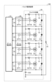
- FIG. 1 is a diagram showing a configuration example of a pulse power supply device 100 according to the first embodiment.
- the pulse power supply device 100 includes a gate power supply section 10, a gate control section 20, a Marx circuit 30, and a load R1.
- the Marx circuit 30 includes a DC power supply VDC, insulating inductors L1 to L4, capacitors C1 to C4, gate drive circuits GATE1 to GATE4, semiconductor switches Q1 to Q4, and diodes D1 to D4.
- the gate power supply section 10 generates a gate power source, which is a drive power source for driving the semiconductor switches Q1 to Q4, for the gate drive circuits GATE1 to GATE4 included in the Marx circuit 30, and supplies it to the gate drive circuits GATE1 to GATE4.
- the gate power supply unit 10 generates an insulated gate power supply for the gate drive circuits GATE1 to GATE4. The detailed configuration and operation of the gate power supply unit 10 will be described later.
- the gate control unit 20 generates drive signals for controlling the operations of the gate drive circuits GATE1 to GATE4.
- the gate control unit 20 controls on/off of the semiconductor switches Q1 to Q4 by generating drive signals for the gate drive circuits GATE1 to GATE4.
- the gate control section 20 includes control sections OPT1 to OPT4.
- the control unit OPT1 generates a drive signal for the gate drive circuit GATE1
- the control unit OPT2 generates a drive signal for the gate drive circuit GATE2
- the control unit OPT3 generates a drive signal for the gate drive circuit GATE2.
- a drive signal for GATE3 is generated
- a control unit OPT4 generates a drive signal for gate drive circuit GATE4.
- a DC power supply VDC charges a plurality of capacitors C1 to C4 in parallel through a plurality of insulating inductors L1 to L4, and synchronizes a plurality of semiconductor switches Q1 to Q4 to make them conductive.
- This circuit discharges all the capacitors C1 to C4 in series and generates a high voltage to the load R1.
- the insulating inductors L1 to L4 insulate the DC power supply VDC and the capacitors C1 to C4.
- the gate drive circuits GATE1 to GATE4 drive the semiconductor switches Q1 to Q4 using the gate power supplied from the gate power supply section 10 based on the drive signal from the gate control section 20.
- the semiconductor switches Q1 to Q4 are arranged in the Marx circuit 30 so as to connect the capacitors C1 to C4 in series when in a conductive state, and can control the capacitors C1 to C4 to be discharged.
- the Marx circuit 30 can generate a desired high-voltage pulse by connecting a module including an insulating inductor Ln, a capacitor Cn, a gate drive circuit GATEn, a semiconductor switch Qn, and a diode Dn in multiple stages. It is possible. “n” of the capacitor Cn, etc. is a positive integer whose maximum value is the number of stages of the Marx circuit 30.
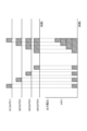
- the pulse power supply device 100 does not need to operate all the semiconductor switches Q1 to Q4 included in the Marx circuit 30 at the same time, and can achieve a desired output voltage waveform by changing the operation timing of the semiconductor switches Q1 to Q4 as shown in FIG. It is possible to change to Operating the semiconductor switches Q1 to Q4 means to turn on the semiconductor switches Q1 to Q4, and to make the semiconductor switches Q1 to Q4 conductive.
- FIG. 2 is a diagram showing the relationship between the operation timings of the semiconductor switches Q1 to Q4 and the output voltage waveform in the Marx circuit 30 of the pulse power supply device 100 according to the first embodiment. In FIG.
- the upper diagram shows the timing at which the semiconductor switches Q1 to Q4 are turned on, that is, the timing at which the gate drive circuits GATE1 to GATE4 output on, ie, conductive gate signals to the semiconductor switches Q1 to Q4.
- the lower diagram shows the voltage applied to the load R1, that is, the output voltage v from the Marx circuit 30.
- the output voltage v is added by the number of stages that are turned on, that is, conductive, among the semiconductor switches Q1 to Q4.
- the Marx circuit 30 can generate a stepped voltage waveform by, for example, delaying the turn-on timing of the semiconductor switches Q1 to Q4 by a certain period of time.
- the diode Dn is conductive when the semiconductor switch Qn is off, that is, in a non-conductive stage. Therefore, the Marx circuit 30 is characterized in that even if the semiconductor switch Qn malfunctions, the semiconductor switch Qn is unlikely to fail.
- a drive signal is generated by the gate control unit 20, and the semiconductor switches Q1 to Q4 are driven by gate drive circuits GATE1 to GATE4.
- the gate power supply for the gate drive circuits GATE1 to GATE4 is generated by the gate power supply unit 10.
- MOSFETs Metal Oxide Semiconductor Field Effect Transistors
- IGBTs Insulated Gate Bipolar Transistors
- the semiconductor switches Q1 to Q4 can achieve faster speeds, lower losses, higher voltages, etc. by changing the semiconductor material from conventional Si (Silicon) to SiC (Silicon Carbide), GaN (Gallium Nitride), etc. becomes possible.
- MOSFETs are used in the semiconductor switches Q1 to Q4. Since the MOSFETs are gate voltage driven devices, in order to turn the switches on, that is, to make them conductive, the gate potential must be higher than the gate threshold voltage with respect to the source potential. There is a need to.
- the gate power supply unit 10 requires as many power supplies as the number of stages of the Marx circuit 30, which are insulated with a high withstand voltage from GND, that is, the power supply is floating.
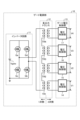
- FIG. 3 is a diagram showing a configuration example of the gate power supply section 10 included in the pulse power supply device 100 according to the first embodiment.
- the gate power supply section 10 includes an inverter circuit 11, a multi-output transformer 12, and a gate voltage control section 13.
- the inverter circuit 11 includes a DC power supply Vgate and switching elements Qa to Qd.
- the inverter circuit 11 converts the DC voltage output from the DC power supply Vgate into an AC voltage through switching operations of the switching elements Qa to Qd.
- the configuration of the inverter circuit 11 is not limited to the example shown in FIG.
- the inverter circuit 11 may have a configuration different from that in FIG. 3 as long as it can output an AC voltage.
- the inverter circuit 11 is an AC power source that outputs a high frequency AC voltage of about 100 kHz to the multi-output transformer 12, for example.
- the multi-output transformer 12 includes transformers TR1 to TR4 whose primary sides are commonly connected to the inverter circuit 11 and whose secondary sides generate independent gate power supplies for each stage of the Marx circuit 30.
- the primary side of the multi-output transformer 12 is driven by the inverter circuit 11.
- the secondary side of the multi-output transformer 12 is configured to be parallelized by the number of stages of the Marx circuit 30.
- the multi-output transformer 12 has a primary side and a secondary side insulated, and generates gate power for each stage of the Marx circuit 30 from the high-frequency AC voltage output from the inverter circuit 11.
- the inverter circuit 11 outputs an alternating current voltage at a high frequency of about 100 kHz, so that the magnetic core can be miniaturized.
- the multi-output transformer 12 can be made smaller by using a small magnetic core, and as a result, the stray capacitance between the primary side and the secondary side can be reduced. is possible.
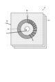
- FIG. 4 is a diagram showing a configuration example of the multi-output transformer 12 of the gate power supply section 10 included in the pulse power supply device 100 according to the first embodiment.
- the multi-output transformer 12 uses a toroidal-shaped magnetic core 62, and a primary winding 63 on the primary side passes through the center of the magnetic core 62. An insulation distance from the secondary winding 64 on the secondary side wound around the body core 62 can be maintained.
- FIG. 4 is a diagram showing a configuration example of the multi-output transformer 12 of the gate power supply section 10 included in the pulse power supply device 100 according to the first embodiment.
- the multi-output transformer 12 uses a toroidal-shaped magnetic core 62, and a primary winding 63 on the primary side passes through the center of the magnetic core 62. An insulation distance from the secondary winding 64 on the secondary side wound around the body core 62 can be maintained.
- FIG. 4 is a diagram showing a configuration example of the multi-output transformer 12 of the gate power supply section 10 included in the
- the substrate 61 has a magnetic core 62 mounted thereon, and the multi-output transformer 12 includes as many substrates 61 as the number of stages of the Marx circuit 30. That is, the multi-output transformer 12 connects a substrate 61, on which a toroidal-shaped magnetic core 62 and a secondary winding 64 wound around the magnetic core 62 are mounted, to a plurality of capacitors C1 to C1 of the Marx circuit 30. Provide as many stages as C4. A primary winding 63 on the primary side is passed through the penetrating portion of the magnetic core 62 of each board 61 .
- the multi-output transformer 12 can reduce stray capacitance between the primary side and the secondary side by intentionally making the primary winding 63 one turn or two turns to worsen the magnetic coupling. is possible. That is, in the multi-output transformer 12, the number of turns of the primary winding 63 on the primary side is 1 or 2. By reducing stray capacitance, the multi-output transformer 12 makes it difficult for common mode noise to propagate between the primary side and the secondary side.
- the voltage control units 14 to 17 included in the gate voltage control unit 13 are connected to the output end of the secondary side of the multi-output transformer 12.
- the voltage control unit 14 is connected to the transformer TR1 of the multi-output transformer 12
- the voltage control unit 15 is connected to the transformer TR2 of the multi-output transformer 12
- the voltage control unit 16 is connected to the transformer TR3 of the multi-output transformer 12.
- the voltage control section 17 is connected to the transformer TR4 of the multi-output transformer 12.
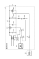
- the voltage control section 14 includes a diode bridge DB1, capacitors C11 and C12, transistors T11 and T12, resistors R11 and R12, a gate voltage command section 51, a logic inversion section 52, and an operational amplifier OP1.
- the diode bridge DB1 rectifies the AC voltage output from the transformer TR1 of the multi-output transformer 12.
- Capacitor C11 smoothes the rectified voltage after rectification by diode bridge DB1.
- the voltage control section 14 performs output voltage feedback to control the base current of the transistor T11 to the voltage commanded by the gate voltage command section 51 using the resistors R11, R12 and the operational amplifier OP1. Thereby, the voltage control unit 14 generates a stable gate voltage, that is, a gate power supply.
- the voltage control unit 14 controls the gate voltage of the gate power supply to, for example, 15V, which is necessary for the gate drive circuit GATE1 to drive the semiconductor switch Q1.
- the voltage control unit 14 supplies the voltage across the capacitor C12, which is the voltage stored in the capacitor C12 after passing through the transistor T11, that is, the voltage across the transistor T12, to the gate drive circuit GATE1 of the Marx circuit 30 as a gate power supply. .
- the gate power supply section 10 when some of the semiconductor switches Qn of the Marx circuit 30 operate, that is, are turned on, in the gate power supply section 10, a load is applied only to the output end of the stage where the semiconductor switches Qn are turned on, and the semiconductor switches Qn are turned on.
- the load at the output end of the stage that is off is zero.
- the output end of the gate power supply section 10 is the output end of the voltage control sections 14 to 17 included in the gate voltage control section 13 shown in FIG. 3, that is, the portion of the output voltages V1 to V4 shown in FIG.
- the gate power supply unit 10 cannot output to each stage of the Marx circuit 30 with only the above control.
- the output of the gate power supply cannot be set to the same voltage. If the gate power supply unit 10 is controlled only by the above-described control, the output voltage will vary depending on the number of turned-on stages of the semiconductor switches Qn, so it will be difficult to supply a stable gate voltage, that is, a gate power supply.
- the pulse power supply device 100 when an overvoltage is applied from the gate power supply section 10 to the gate drive circuits GATE1 to GATE4 of the Marx circuit 30, the gate drive circuit There is a possibility that GATE1 to GATE4 will fail. Therefore, in the present embodiment, the load at the output ends of the voltage control units 14 to 17 included in the gate voltage control unit 13, that is, the load at the output end of the gate power supply unit 10, is Control by action.
- the gate voltage control unit 13 is connected to the secondary side of the multi-output transformer 12, and controls the first power consumption in the gate voltage control unit 13 when the semiconductor switch Qn is non-conducting, and the first power consumption when the semiconductor switch Qn is conductive.
- the first power consumption is controlled so that the difference from the second power consumption in the Marx circuit 30 caused by the switch Qn is within a specified range. That is, the gate voltage control unit 13 controls the voltage control units 14 to 17 to consume power for each stage of the Marx circuit 30 when the Marx circuit 30 does not consume power, based on the on/off status of the semiconductor switches Q1 to Q4. However, when the Marx circuit 30 consumes power, the corresponding voltage control sections 14 to 17 control the power so as not to consume it.
- the gate voltage control section 13 obtains drive signals for the semiconductor switches Q1 to Q4 from the gate control section 20, which generates drive signals for the semiconductor switches Q1 to Q4.
- the gate voltage control unit 13 outputs each of the acquired drive signals for the semiconductor switches Q1 to Q4 to the corresponding voltage control units 14 to 17. That is, the voltage control units 14 to 17 obtain drive signals for the corresponding semiconductor switches Q1 to Q4 from the gate control unit 20.
- the logic inversion unit 52 inverts the transistor T12 with a control signal to turn on the transistor T12 in response to the OFF drive signal. Output.
- the logic inversion unit 52 adjusts the load resistance of the transistor T12 to the same level as the load resistance of the Marx circuit 30 when the semiconductor switch Q1 is on, in accordance with the timing when the gate drive circuit GATE1 is turned off, that is, the semiconductor switch Q1 is turned off.
- the base current of transistor T12 is controlled so that In the voltage control unit 14, the transistor T12 behaves like a dummy resistor when the semiconductor switch Q1 is off.
- the logic inversion unit 52 inverts the transistor T12 with a control signal to turn off the transistor T12 in response to the ON drive signal. Output.
- the transistor T12 does not need to behave like a dummy resistor when the gate drive circuit GATE1 is on, that is, the semiconductor switch Q1 is on. Therefore, the logic inversion unit 52 controls the base current of the transistor T12 so that the load resistance of the transistor T12 is small, that is, close to 0, in accordance with the turn-on timing of the semiconductor switch Q1.
- the transistor T12 is controlled so that the power consumption in the transistor T12 and the power consumption generated when driving the semiconductor switch Q1 of the Marx circuit 30 are equal to each other. Adjust the resistance value of the dummy resistor by T12. If the resistance value of the transistor T12 is too large, the power loss in the gate voltage control section 13 will increase, which is not preferable. Therefore, the voltage control unit 14 lowers the base current of the transistor T12 to turn off the transistor T12 when the semiconductor switch Q1 is not driven.
- the gate power supply section 10 of the pulse power supply device 100 stabilizes the multiple output voltages on the secondary side of the multiple output transformer 12, that is, the output voltages of the transformers TR1 to TR4, without becoming unbalanced.
- a stable gate power supply can be supplied to each of the 30 stages.
- the gate voltage control section 13 has a transistor T12 that can play the role of a dummy resistor for each output terminal of the gate power supply for the gate drive circuits GATE1 to GATE4.
- the gate voltage control section 13 controls the base current supplied to the transistor T12 based on the drive signal obtained from the gate control section 20. That is, the gate voltage control unit 13 turns off the transistor T12 at the output end corresponding to the gate drive circuit GATEn that turns on the semiconductor switch Qn by the drive signal. In addition, the gate voltage control unit 13 turns on the transistor T12 at the output end corresponding to the gate drive circuit GATEn that makes the semiconductor switch Qn non-conductive using the drive signal, thereby controlling the resistance value of the transistor T12 that serves as a dummy resistor.
- FIG. 6 shows the operation timing of the semiconductor switches Q1 to Q4 in the Marx circuit 30 of the pulse power supply device 100 according to the first embodiment and the timing of the operation of the transistors T12 of each voltage control section 14 to 17 in the gate voltage control section 13 of the gate power supply section 10.
- FIG. 3 is a diagram showing the relationship with operation timing.
- FIG. 6 shows that the voltage control units 14 to 17 of the gate voltage control unit 13 turn on the transistor T12 when the corresponding semiconductor switches Q1 to Q4 in the Marx circuit 30 are off, and This shows a state in which transistor T12 is turned off when Q4 is on.
- the gate power supply section 10 operates on each of the multi-output transformers 12, regardless of whether or not the semiconductor switches Q1 to Q4 of the Marx circuit 30 perform switching operations.
- the gate voltage control unit 13 controls the dummy resistance of the transistor T12 at the output end of the gate power supply supplied to the gate drive circuits GATE1 to GATE4 so that the current in the transformers TR1 to TR4 is constant. Thereby, the gate power supply section 10 can control the output voltage of the multi-output transformer 12 to be constant.
- the gate power supply unit 10 prevents an imbalance in the gate power supplied to the gate drive circuits GATE1 to GATE4 to drive the semiconductor switches Q1 to Q4 of the Marx circuit 30, and prevents failures of the gate drive circuits GATE1 to GATE4.
- This allows the pulse power supply device 100 to generate stable high voltage pulses. In this way, the pulse power supply device 100 can suppress imbalance in the voltages supplied for driving the plurality of semiconductor switches Q1 to Q4 of the Marx circuit 30.
- each of the voltage control sections 14 to 17 of the gate voltage control section 13 controls the gate power supplied to each stage of the Marx circuit 30 using transistors so that the same gate power is supplied.
- each voltage control section 14 to 17 of the gate voltage control section 13 uses a MOSFET instead of a transistor.
- the MOSFET will be referred to as a field effect transistor or a metal oxide semiconductor field effect transistor.
- the configuration of the pulse power supply device 100 is similar to the configuration of the pulse power supply device 100 in the first embodiment shown in FIG.
- the configuration of the gate power supply unit 10 is similar to the configuration of the gate power supply unit 10 in the first embodiment shown in FIG.
- the configurations of the voltage control sections 14 to 17 included in the gate voltage control section 13 will be explained. Since the voltage control units 14 to 17 have similar configurations, the voltage control unit 14 will be explained here as an example.
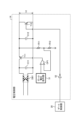
- FIG. 7 is a diagram showing a configuration example of the voltage control section 14 included in the gate voltage control section 13 of the gate power supply section 10 included in the pulse power supply device 100 according to the second embodiment.
- the voltage control section 14 includes a diode bridge DB1, capacitors C11 and C12, field effect transistors M11 and M12, a diode D11, an inductor L11, resistors R11 and R12, a logic inversion section 52, and a gate voltage command section 53. , an oscillator 54, and operational amplifiers OP2 and OP3.
- the diode bridge DB1 rectifies the AC voltage output from the transformer TR1 of the multi-output transformer 12.
- Capacitor C11 smoothes the rectified voltage after rectification by diode bridge DB1.
- the voltage control unit 14 uses the diode D11, the inductor L11, the resistors R11, R12, the operational amplifiers OP2, OP3, and the oscillator 54 to command the switching pulse width of the field effect transistor M11 by the gate voltage command unit 53. Output voltage feedback is performed by controlling the output voltage to a certain width. Thereby, the voltage control unit 14 generates a stable gate voltage, that is, a gate power supply.
- the voltage control unit 14 uses the voltage across the capacitor C12, which is the voltage stored in the capacitor C12 after passing through the field effect transistor M11, the diode D11, and the inductor L11, that is, the voltage across the field effect transistor M12, as a gate power supply. It is supplied to the gate drive circuit GATE1 of the Marx circuit 30.
- the gate power supply section 10 when some of the semiconductor switches Qn of the Marx circuit 30 operate, that is, turn on, the gate power supply section 10 applies a load only to the output end of the stage where the semiconductor switches Qn are turned on.
- the load at the output end of the stage in which the semiconductor switch Qn is turned off is zero. Since the output voltage of the secondary side of the multi-output transformer 12, that is, the output voltage of the transformers TR1 to TR4, will be unbalanced, the gate power supply unit 10 cannot output to each stage of the Marx circuit 30 with only the above control. The output of the gate power supply cannot be set to the same voltage.
- the output voltage will vary depending on the number of turned-on stages of the semiconductor switches Qn, so it will be difficult to supply a stable gate voltage, that is, a gate power supply. Therefore, in the present embodiment, the load at the output ends of the voltage control units 14 to 17 included in the gate voltage control unit 13, that is, the load at the output end of the gate power supply unit 10, is Control by action.
- the gate voltage control section 13 obtains drive signals for the semiconductor switches Q1 to Q4 from the gate control section 20, which generates drive signals for the semiconductor switches Q1 to Q4.
- the gate voltage control unit 13 outputs each of the acquired drive signals for the semiconductor switches Q1 to Q4 to the corresponding voltage control units 14 to 17. That is, the voltage control units 14 to 17 obtain drive signals for the corresponding semiconductor switches Q1 to Q4 from the gate control unit 20.
- the logic inversion unit 52 inverts the control signal to turn on the field effect transistor M12 in response to the OFF drive signal. Output to effect transistor M12.
- the logic inversion unit 52 adjusts the load resistance of the field effect transistor M12 to be the same as the load resistance of the Marx circuit 30 when the semiconductor switch Q1 is on, in accordance with the timing when the gate drive circuit GATE1 is off, that is, the semiconductor switch Q1 is off.
- the gate voltage of the field effect transistor M12 is controlled so as to maintain the same level. In the voltage control section 14, the field effect transistor M12 behaves like a dummy resistor when the semiconductor switch Q1 is off.
- the logic inversion unit 52 inverts the control signal to turn off the field effect transistor M12 in accordance with the ON drive signal. Output to effect transistor M12.
- the field effect transistor M12 does not need to behave like a dummy resistor when the gate drive circuit GATE1 is on, that is, the semiconductor switch Q1 is on. Therefore, the logic inverting unit 52 controls the gate voltage of the field effect transistor M12 so that the load resistance of the field effect transistor M12 is small, that is, close to 0, in accordance with the turn-on timing of the semiconductor switch Q1.
- the power consumption in the field effect transistor M12 and the power consumption generated when driving the semiconductor switch Q1 of the Marx circuit 30 are equal.
- the resistance value of the dummy resistor by the field effect transistor M12 is adjusted so that If the resistance value of the field effect transistor M12 is too large, the power loss in the gate voltage control section 13 will increase, which is not preferable. Therefore, the voltage control unit 14 lowers the gate voltage of the field effect transistor M12 to turn off the field effect transistor M12 when the semiconductor switch Q1 is not driven.
- the gate power supply section 10 of the pulse power supply device 100 stabilizes the multiple output voltages on the secondary side of the multiple output transformer 12, that is, the output voltages of the transformers TR1 to TR4, without becoming unbalanced.
- a stable gate power supply can be supplied to each of the 30 stages.
- the gate voltage control section 13 has a field effect transistor M12 that can play the role of a dummy resistor for each output terminal of the gate power supply for the gate drive circuits GATE1 to GATE4.
- the gate voltage control section 13 controls the gate voltage supplied to the field effect transistor M12 based on the drive signal acquired from the gate control section 20. That is, the gate voltage control section 13 turns off the field effect transistor M12 at the output end corresponding to the gate drive circuit GATEn that turns on the semiconductor switch Qn by the drive signal.
- the gate voltage control unit 13 turns on the field effect transistor M12 at the output end corresponding to the gate drive circuit GATEn that makes the semiconductor switch Qn non-conductive by the drive signal, and changes the resistance value of the field effect transistor M12 that becomes a dummy resistance. Control.
- the gate power supply section 10 operates on each of the multi-output transformers 12, regardless of whether or not the semiconductor switches Q1 to Q4 of the Marx circuit 30 perform switching operations.
- the gate voltage control unit 13 controls the dummy resistance of the field effect transistor M12 at the output end of the gate power supply supplied to the gate drive circuits GATE1 to GATE4. Even in this case, the gate power supply section 10 can obtain the same effects as in the first embodiment.
Landscapes
- Engineering & Computer Science (AREA)
- Power Engineering (AREA)
- Dc-Dc Converters (AREA)
- Generation Of Surge Voltage And Current (AREA)
Priority Applications (2)
| Application Number | Priority Date | Filing Date | Title |
|---|---|---|---|
| JP2024540091A JP7749139B2 (ja) | 2022-08-08 | 2022-08-08 | パルス電源装置 |
| PCT/JP2022/030295 WO2024033977A1 (ja) | 2022-08-08 | 2022-08-08 | パルス電源装置 |
Applications Claiming Priority (1)
| Application Number | Priority Date | Filing Date | Title |
|---|---|---|---|
| PCT/JP2022/030295 WO2024033977A1 (ja) | 2022-08-08 | 2022-08-08 | パルス電源装置 |
Publications (1)
| Publication Number | Publication Date |
|---|---|
| WO2024033977A1 true WO2024033977A1 (ja) | 2024-02-15 |
Family
ID=89851228
Family Applications (1)
| Application Number | Title | Priority Date | Filing Date |
|---|---|---|---|
| PCT/JP2022/030295 Ceased WO2024033977A1 (ja) | 2022-08-08 | 2022-08-08 | パルス電源装置 |
Country Status (2)
| Country | Link |
|---|---|
| JP (1) | JP7749139B2 (cg-RX-API-DMAC7.html) |
| WO (1) | WO2024033977A1 (cg-RX-API-DMAC7.html) |
Citations (4)
| Publication number | Priority date | Publication date | Assignee | Title |
|---|---|---|---|---|
| JPH0837775A (ja) * | 1994-07-22 | 1996-02-06 | Toshiba Corp | 電力変換装置 |
| JP2006116555A (ja) * | 2004-10-19 | 2006-05-11 | Sansha Electric Mfg Co Ltd | アーク応用機器の電源装置 |
| JP2007536890A (ja) * | 2004-05-04 | 2007-12-13 | スタンガネス インダストリーズ インコーポレイテッド | 固体スイッチを用いた高電圧パルス電源 |
| WO2015115226A1 (ja) * | 2014-01-28 | 2015-08-06 | アイシン・エィ・ダブリュ株式会社 | 電力変換装置 |
-
2022
- 2022-08-08 JP JP2024540091A patent/JP7749139B2/ja active Active
- 2022-08-08 WO PCT/JP2022/030295 patent/WO2024033977A1/ja not_active Ceased
Patent Citations (4)
| Publication number | Priority date | Publication date | Assignee | Title |
|---|---|---|---|---|
| JPH0837775A (ja) * | 1994-07-22 | 1996-02-06 | Toshiba Corp | 電力変換装置 |
| JP2007536890A (ja) * | 2004-05-04 | 2007-12-13 | スタンガネス インダストリーズ インコーポレイテッド | 固体スイッチを用いた高電圧パルス電源 |
| JP2006116555A (ja) * | 2004-10-19 | 2006-05-11 | Sansha Electric Mfg Co Ltd | アーク応用機器の電源装置 |
| WO2015115226A1 (ja) * | 2014-01-28 | 2015-08-06 | アイシン・エィ・ダブリュ株式会社 | 電力変換装置 |
Also Published As
| Publication number | Publication date |
|---|---|
| JPWO2024033977A1 (cg-RX-API-DMAC7.html) | 2024-02-15 |
| JP7749139B2 (ja) | 2025-10-03 |
Similar Documents
| Publication | Publication Date | Title |
|---|---|---|
| US10003267B1 (en) | Isolated DC-DC converter with an H-bridge circuit | |
| KR101016901B1 (ko) | 용량성 부하를 위한 전원 공급 장치 및 그 동작 방법 | |
| CN115191079B (zh) | 在加电期间使用开关路径对谐振转换器的控制 | |
| EP2915245A2 (en) | Self-oscillating resonant power converter | |
| TW202236793A (zh) | 雙極脈衝電壓閘極驅動器 | |
| US20090102443A1 (en) | H-bridge pulse generator | |
| KR20030047762A (ko) | 사인형 반파 공진 구동 회로 | |
| JP6424533B2 (ja) | 電圧共振型インバータ装置及びその制御方法と表面改質装置 | |
| US7589301B2 (en) | Induction heating device having plural resonant circuits | |
| JP6186392B2 (ja) | 電流共振型dc−dcコンバータ | |
| JP7749139B2 (ja) | パルス電源装置 | |
| CN1771655A (zh) | 自适应性谐振开关电源系统 | |
| EP3934074B1 (en) | Power supply device without ringing effect | |
| JP2002017090A (ja) | 圧電トランスの駆動方法および駆動装置 | |
| CN101501974A (zh) | 具有磁耦合的开关控制电路的dc-dc电功率变换器 | |
| JP2019054349A (ja) | ゲート駆動回路、および、パワースイッチングシステム | |
| KR101101428B1 (ko) | 반복 전압 펄스들을 사용하여 동작될 램프를 위한 전자식 안정기 | |
| JP2009268206A (ja) | 交流電源装置 | |
| CN104953994B (zh) | 一种功率开关管的驱动电路 | |
| US20210111708A1 (en) | Driving circuit of an electrostatic adhesion board and an electrostatic adhesion apparatus using the driving circuit | |
| US7564673B2 (en) | Control circuit for converters | |
| CN114285300A (zh) | 消除振铃效应的电源供应器 | |
| US12149159B2 (en) | Driving circuit of power devices, switching circuit and power conversion circuit | |
| JP2025059935A (ja) | インバータ装置 | |
| CN119836737A (zh) | 带有可变谐振频率的llc谐振转换器 |
Legal Events
| Date | Code | Title | Description |
|---|---|---|---|
| 121 | Ep: the epo has been informed by wipo that ep was designated in this application |
Ref document number: 22954899 Country of ref document: EP Kind code of ref document: A1 |
|
| ENP | Entry into the national phase |
Ref document number: 2024540091 Country of ref document: JP Kind code of ref document: A |
|
| NENP | Non-entry into the national phase |
Ref country code: DE |
|
| 122 | Ep: pct application non-entry in european phase |
Ref document number: 22954899 Country of ref document: EP Kind code of ref document: A1 |