WO2024029628A1 - Wiring board, electronic component mounting package using wiring board, and electronic module - Google Patents
Wiring board, electronic component mounting package using wiring board, and electronic module Download PDFInfo
- Publication number
- WO2024029628A1 WO2024029628A1 PCT/JP2023/028615 JP2023028615W WO2024029628A1 WO 2024029628 A1 WO2024029628 A1 WO 2024029628A1 JP 2023028615 W JP2023028615 W JP 2023028615W WO 2024029628 A1 WO2024029628 A1 WO 2024029628A1
- Authority
- WO
- WIPO (PCT)
- Prior art keywords
- line
- opening
- wiring board
- plan
- view
- Prior art date
Links
- 239000004020 conductor Substances 0.000 claims abstract description 120
- 239000000758 substrate Substances 0.000 claims description 16
- 239000010410 layer Substances 0.000 description 57
- 239000000463 material Substances 0.000 description 31
- PXHVJJICTQNCMI-UHFFFAOYSA-N Nickel Chemical compound [Ni] PXHVJJICTQNCMI-UHFFFAOYSA-N 0.000 description 16
- 239000007769 metal material Substances 0.000 description 11
- 238000000034 method Methods 0.000 description 9
- XEEYBQQBJWHFJM-UHFFFAOYSA-N Iron Chemical compound [Fe] XEEYBQQBJWHFJM-UHFFFAOYSA-N 0.000 description 8
- 229910052759 nickel Inorganic materials 0.000 description 8
- 230000003287 optical effect Effects 0.000 description 7
- RYGMFSIKBFXOCR-UHFFFAOYSA-N Copper Chemical compound [Cu] RYGMFSIKBFXOCR-UHFFFAOYSA-N 0.000 description 6
- 229910052802 copper Inorganic materials 0.000 description 6
- 239000010949 copper Substances 0.000 description 6
- 229910052751 metal Inorganic materials 0.000 description 6
- 239000002184 metal Substances 0.000 description 6
- ZOKXTWBITQBERF-UHFFFAOYSA-N Molybdenum Chemical compound [Mo] ZOKXTWBITQBERF-UHFFFAOYSA-N 0.000 description 5
- 229910052750 molybdenum Inorganic materials 0.000 description 5
- 239000011733 molybdenum Substances 0.000 description 5
- 239000004065 semiconductor Substances 0.000 description 5
- WFKWXMTUELFFGS-UHFFFAOYSA-N tungsten Chemical compound [W] WFKWXMTUELFFGS-UHFFFAOYSA-N 0.000 description 5
- 229910052721 tungsten Inorganic materials 0.000 description 5
- 239000010937 tungsten Substances 0.000 description 5
- 229910045601 alloy Inorganic materials 0.000 description 4
- 239000000956 alloy Substances 0.000 description 4
- 229910017052 cobalt Inorganic materials 0.000 description 4
- 239000010941 cobalt Substances 0.000 description 4
- GUTLYIVDDKVIGB-UHFFFAOYSA-N cobalt atom Chemical compound [Co] GUTLYIVDDKVIGB-UHFFFAOYSA-N 0.000 description 4
- PCHJSUWPFVWCPO-UHFFFAOYSA-N gold Chemical compound [Au] PCHJSUWPFVWCPO-UHFFFAOYSA-N 0.000 description 4
- 229910052737 gold Inorganic materials 0.000 description 4
- 239000010931 gold Substances 0.000 description 4
- 229910052742 iron Inorganic materials 0.000 description 4
- 229910052581 Si3N4 Inorganic materials 0.000 description 3
- BQCADISMDOOEFD-UHFFFAOYSA-N Silver Chemical compound [Ag] BQCADISMDOOEFD-UHFFFAOYSA-N 0.000 description 3
- 238000005219 brazing Methods 0.000 description 3
- 229910010293 ceramic material Inorganic materials 0.000 description 3
- 238000004891 communication Methods 0.000 description 3
- PMHQVHHXPFUNSP-UHFFFAOYSA-M copper(1+);methylsulfanylmethane;bromide Chemical compound Br[Cu].CSC PMHQVHHXPFUNSP-UHFFFAOYSA-M 0.000 description 3
- KZHJGOXRZJKJNY-UHFFFAOYSA-N dioxosilane;oxo(oxoalumanyloxy)alumane Chemical compound O=[Si]=O.O=[Si]=O.O=[Al]O[Al]=O.O=[Al]O[Al]=O.O=[Al]O[Al]=O KZHJGOXRZJKJNY-UHFFFAOYSA-N 0.000 description 3
- 239000010408 film Substances 0.000 description 3
- 229910052863 mullite Inorganic materials 0.000 description 3
- TWNQGVIAIRXVLR-UHFFFAOYSA-N oxo(oxoalumanyloxy)alumane Chemical compound O=[Al]O[Al]=O TWNQGVIAIRXVLR-UHFFFAOYSA-N 0.000 description 3
- 238000007747 plating Methods 0.000 description 3
- 102200069890 rs104893963 Human genes 0.000 description 3
- HBMJWWWQQXIZIP-UHFFFAOYSA-N silicon carbide Chemical compound [Si+]#[C-] HBMJWWWQQXIZIP-UHFFFAOYSA-N 0.000 description 3
- 229910010271 silicon carbide Inorganic materials 0.000 description 3
- HQVNEWCFYHHQES-UHFFFAOYSA-N silicon nitride Chemical compound N12[Si]34N5[Si]62N3[Si]51N64 HQVNEWCFYHHQES-UHFFFAOYSA-N 0.000 description 3
- 229910052709 silver Inorganic materials 0.000 description 3
- 239000004332 silver Substances 0.000 description 3
- 239000002356 single layer Substances 0.000 description 3
- VYZAMTAEIAYCRO-UHFFFAOYSA-N Chromium Chemical compound [Cr] VYZAMTAEIAYCRO-UHFFFAOYSA-N 0.000 description 2
- 102220498131 Transmembrane 4 L6 family member 20_G22L_mutation Human genes 0.000 description 2
- 229910052804 chromium Inorganic materials 0.000 description 2
- 239000011651 chromium Substances 0.000 description 2
- 230000000694 effects Effects 0.000 description 2
- 239000002241 glass-ceramic Substances 0.000 description 2
- 239000011810 insulating material Substances 0.000 description 2
- 239000011347 resin Substances 0.000 description 2
- 229920005989 resin Polymers 0.000 description 2
- 102220071758 rs794728545 Human genes 0.000 description 2
- 230000008054 signal transmission Effects 0.000 description 2
- 229910000679 solder Inorganic materials 0.000 description 2
- JBRZTFJDHDCESZ-UHFFFAOYSA-N AsGa Chemical compound [As]#[Ga] JBRZTFJDHDCESZ-UHFFFAOYSA-N 0.000 description 1
- 229910002601 GaN Inorganic materials 0.000 description 1
- 229910001218 Gallium arsenide Inorganic materials 0.000 description 1
- JMASRVWKEDWRBT-UHFFFAOYSA-N Gallium nitride Chemical compound [Ga]#N JMASRVWKEDWRBT-UHFFFAOYSA-N 0.000 description 1
- FYYHWMGAXLPEAU-UHFFFAOYSA-N Magnesium Chemical compound [Mg] FYYHWMGAXLPEAU-UHFFFAOYSA-N 0.000 description 1
- PWHULOQIROXLJO-UHFFFAOYSA-N Manganese Chemical compound [Mn] PWHULOQIROXLJO-UHFFFAOYSA-N 0.000 description 1
- OAICVXFJPJFONN-UHFFFAOYSA-N Phosphorus Chemical compound [P] OAICVXFJPJFONN-UHFFFAOYSA-N 0.000 description 1
- 239000000654 additive Substances 0.000 description 1
- 239000000853 adhesive Substances 0.000 description 1
- 230000001070 adhesive effect Effects 0.000 description 1
- 229910052782 aluminium Inorganic materials 0.000 description 1
- XAGFODPZIPBFFR-UHFFFAOYSA-N aluminium Chemical compound [Al] XAGFODPZIPBFFR-UHFFFAOYSA-N 0.000 description 1
- PNEYBMLMFCGWSK-UHFFFAOYSA-N aluminium oxide Inorganic materials [O-2].[O-2].[O-2].[Al+3].[Al+3] PNEYBMLMFCGWSK-UHFFFAOYSA-N 0.000 description 1
- 230000005540 biological transmission Effects 0.000 description 1
- 229910052793 cadmium Inorganic materials 0.000 description 1
- BDOSMKKIYDKNTQ-UHFFFAOYSA-N cadmium atom Chemical compound [Cd] BDOSMKKIYDKNTQ-UHFFFAOYSA-N 0.000 description 1
- 239000000919 ceramic Substances 0.000 description 1
- 239000011247 coating layer Substances 0.000 description 1
- 238000005260 corrosion Methods 0.000 description 1
- 230000007797 corrosion Effects 0.000 description 1
- 238000010586 diagram Methods 0.000 description 1
- 239000003989 dielectric material Substances 0.000 description 1
- 238000007772 electroless plating Methods 0.000 description 1
- 238000009713 electroplating Methods 0.000 description 1
- 239000011521 glass Substances 0.000 description 1
- 239000006112 glass ceramic composition Substances 0.000 description 1
- 238000005304 joining Methods 0.000 description 1
- 238000010030 laminating Methods 0.000 description 1
- 238000003475 lamination Methods 0.000 description 1
- 229910052749 magnesium Inorganic materials 0.000 description 1
- 239000011777 magnesium Substances 0.000 description 1
- 229910052748 manganese Inorganic materials 0.000 description 1
- 239000011572 manganese Substances 0.000 description 1
- 230000003647 oxidation Effects 0.000 description 1
- 238000007254 oxidation reaction Methods 0.000 description 1
- 229910052698 phosphorus Inorganic materials 0.000 description 1
- 239000011574 phosphorus Substances 0.000 description 1
- 238000003672 processing method Methods 0.000 description 1
- 238000004080 punching Methods 0.000 description 1
- 238000005096 rolling process Methods 0.000 description 1
- 238000007650 screen-printing Methods 0.000 description 1
- 238000005245 sintering Methods 0.000 description 1
- 238000004544 sputter deposition Methods 0.000 description 1
- 239000010409 thin film Substances 0.000 description 1
- 238000007740 vapor deposition Methods 0.000 description 1
Images


Classifications
-
- H—ELECTRICITY
- H01—ELECTRIC ELEMENTS
- H01L—SEMICONDUCTOR DEVICES NOT COVERED BY CLASS H10
- H01L23/00—Details of semiconductor or other solid state devices
- H01L23/02—Containers; Seals
-
- H—ELECTRICITY
- H01—ELECTRIC ELEMENTS
- H01L—SEMICONDUCTOR DEVICES NOT COVERED BY CLASS H10
- H01L23/00—Details of semiconductor or other solid state devices
- H01L23/12—Mountings, e.g. non-detachable insulating substrates
-
- H—ELECTRICITY
- H05—ELECTRIC TECHNIQUES NOT OTHERWISE PROVIDED FOR
- H05K—PRINTED CIRCUITS; CASINGS OR CONSTRUCTIONAL DETAILS OF ELECTRIC APPARATUS; MANUFACTURE OF ASSEMBLAGES OF ELECTRICAL COMPONENTS
- H05K1/00—Printed circuits
- H05K1/02—Details
Definitions
- the present disclosure relates to a wiring board, a package for mounting electronic components using the wiring board, and an electronic module.
- a wiring board includes a first insulating layer, a second insulating layer, a first ground conductor, and a first signal conductor.
- the first insulating layer has a first upper surface and a first lower surface opposite to the first upper surface.
- the second insulating layer is located on the first insulating layer and has a second upper surface and a second lower surface opposite to the second upper surface.
- the first ground conductor has a first opening and a second opening, and is located on the first lower surface.
- the first signal conductor has a first line located on the first upper surface and a second line located on the second lower surface. The first line has a first end and a first line extending from the first end.
- the second line has a second end electrically connected to the first end, and a second line extending from the second end.
- first end and the second end are located within the first opening.
- at least a portion of the second line portion is positioned overlapping the second opening.
- the area of the first opening is larger than the area of the second opening.
- the first ground conductor includes a plurality of second openings.
- the plurality of second openings are spaced apart from each other and are located along the second line portion in plan view.
- the dimensions of the second opening in the direction perpendicular to the direction along the second line portion in plan view are the dimensions of the second opening in the direction perpendicular to the direction along the second line portion. It is larger than the dimension of the second line portion in .
- the distance between the plurality of second openings in the direction along the second line portion is perpendicular to the direction along the second line portion. It is not constant in direction.
- the wiring board of (1) to (5) above includes a pair of second ground conductors located between the first insulating layer and the second insulating layer, and electrically connected to the first ground conductor. We are even more prepared. In plan view, the first signal conductor is located between the pair of second ground conductors.
- the first insulating layer has a first side surface connected to the first upper surface and the first lower surface.
- the second insulating layer has a second side surface that is connected to the second upper surface and the second lower surface and is located inward from the first side surface in plan view.
- the first upper surface has a first region located between the first side surface and the second side surface in plan view.
- the first line extends to the first region in a plan view and has a first connection portion to which an external connection member is connected.
- the first ground conductor has one or more third openings located overlapping the first connection portion in plan view.
- the first insulating layer further includes a recessed portion having an opening in the first region. In plan view, the recess is located overlapping at least a portion of the third opening.
- the wiring boards of (1) to (9) above further include a third ground conductor electrically connected to the first ground conductor and located on the second upper surface.
- the third ground conductor has one or more fourth openings. In plan view, at least a portion of the second line portion is located overlapping the fourth opening. In plan view, the fourth opening has a portion that overlaps at least a portion of the second opening.
- An electronic component mounting package includes the wiring board of (1) to (10) above, a substrate, and a frame.
- the frame is bonded to the top surface of the substrate.
- the wiring board is fixed to the frame.
- An electronic module includes the electronic component mounting package of (11) above, an electronic component, and a lid.
- the electronic component is located on the upper surface of the board and is electrically connected to the wiring board.
- the lid body is located on the frame body and is positioned to cover the inside of the electronic component mounting package.
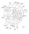
- FIG. 1 is a perspective view of a wiring board, an electronic component mounting package, and an electronic module according to an embodiment of the present disclosure.
- FIG. 2 is an enlarged view of the main part A shown in FIG. 1 viewed from another angle.
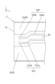
- FIG. 1 is an exploded perspective view of a wiring board according to an embodiment of the present disclosure.
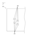
- FIG. 7 is a plan view of a wiring board according to an embodiment of the present disclosure, with a third ground conductor omitted.
- 5 is an enlarged view of main part B shown in FIG. 4.
- FIG. 6 is a diagram showing a third ground conductor superimposed on the enlarged view of FIG. 5.
- FIG. FIG. 3 is a plan view of the first ground conductor. It is a top view of a 1st upper surface. It is a top view of a 2nd upper surface.
- FIG. 3 is a plan view of a third ground conductor.
- the wiring board may be directed either upward or downward, but for convenience, an orthogonal coordinate system xyz is defined and the positive side of the z direction is assumed to be upward.
- the first direction refers to, for example, the y direction in the drawings.
- the second direction intersecting the first direction refers to, for example, the x direction in the drawings.
- the term "inward” refers to, for example, the positive direction of the y-axis in the drawings.
- plan view is a concept that includes plan view.
- FIG. 2 is an enlarged view of a main part A of the wiring board 101, the electronic component mounting package 100, and the electronic module 10 shown in FIG. 1, viewed from the positive direction of the z-axis.
- the wiring board 101 includes a first insulating layer 1, a second insulating layer 2, a first ground conductor G1, and a first signal conductor S1.
- the first insulating layer 1 has a first upper surface 1a and a first lower surface 1b opposite to the first upper surface 1a.
- the material for the first insulating layer 1 include ceramic materials such as aluminum oxide sintered bodies, mullite sintered bodies, silicon carbide sintered bodies, aluminum nitride sintered bodies, and silicon nitride sintered bodies; Dielectric materials such as glass ceramic materials can be used.
- the first insulating layer 1 may be a single layer, or may have a structure in which a plurality of insulating layers are stacked.
- the first insulating layer 1 has, for example, a rectangular shape in plan view, a size of 4 mm x 4 mm to 50 mm x 50 mm, and a thickness of 0.5 mm to 10 mm.
- the second insulating layer 2 is located on the first insulating layer 1 and has a second upper surface 2a and a second lower surface 2b opposite to the second upper surface 2a.
- the material of the second insulating layer 2 may be the same as or different from the material of the first insulating layer 1, and for example, the same material as the first insulating layer 1 described above can be used.
- the second insulating layer 2 may be a single layer or may have a structure in which a plurality of insulating layers are stacked.
- the second insulating layer 2 has, for example, a rectangular shape in a plan view, a size of 4 mm x 4 mm to 50 mm x 50 mm, and a thickness of 0.1 mm to 10 mm.
- the wiring board 101 may further include a third insulating layer 3 located below the first insulating layer 1 (on the first lower surface 1b side).
- the material of the third insulating layer 3 may be the same as or different from the material of the first insulating layer 1, and for example, the same material as the first insulating layer 1 described above can be used.
- the third insulating layer 3 may be a single layer or may have a structure in which a plurality of insulating layers are laminated.
- the third insulating layer 3 has a rectangular shape, for example, in a plan view, with a size of 4 mm x 4 mm to 50 mm x 50 mm, and a thickness of 0.1 mm to 10 mm. Note that wiring such as a signal conductor or a ground conductor may be formed in the third insulating layer 3.
- the first ground conductor G1 has a first opening O1 and a second opening O2, and is located on the first lower surface 1b.
- the material of the first ground conductor G1 include metal materials such as gold, silver, copper, nickel, tungsten, molybdenum, and manganese.
- the first ground conductor G1 may be formed by sintering a metal paste on the first lower surface 1b, or may be formed using a thin film forming technique such as a vapor deposition method or a sputtering method.
- the shape of the first opening O1 may be circular or rectangular in plan view.
- the circular shape mentioned here is not limited to a perfect circle, and may be an elliptical shape or a circle with a part missing.
- the shape of the second opening O2 may also be circular or rectangular in plan view.
- the shape of the first opening O1 and the shape of the second opening O2 may be the same or different.
- the first ground conductor G1 may have a fifth opening O5 and a sixth opening O6.
- the first signal conductor S1 has a first line S11 located on the first upper surface 1a and a second line S12 located on the second lower surface 2b.
- the material of the first signal conductor S1 may be the same as or different from the material of the first ground conductor G1, and for example, the same material as the above-described material of the first ground conductor G1 can be mentioned.
- the first line S11 and the second line S12 do not necessarily need to be made of the same material, and may be made of different materials.
- the first signal conductor S1 may be formed by the same method as the first ground conductor G1 described above.
- the first signal conductor S1 has a width of, for example, 0.05 mm to 2 mm, and a length of 1.5 mm to 25 mm.
- the thickness of the first signal conductor S1 is, for example, 0.01 to 0.1 mm. Note that the width, length, and thickness of the first signal conductor S1 referred to herein can be the dimensions of the first signal conductor S1 in the x direction, the y direction, and the z direction, respectively.
- Metal plating such as nickel plating or gold plating may be formed on the surface of the first signal conductor S1.
- an insulating film made of ceramic (for example, alumina coat) or resin may be located on a part of the first signal conductor S1.
- the insulating film can be provided on the first signal conductor S1 by screen printing. Further, the insulating film may be located only partially on the first signal conductor S1. With such a configuration, it is possible to reduce the possibility that the first signal conductor S1 is short-circuited with other wiring.
- the wiring board 101 may further include a second signal conductor S2 located alongside the first signal conductor S1.
- the first signal conductor S1 and the second signal conductor S2 can be a pair of signal conductors that transmit differential signals.
- the material of the second signal conductor S2 may be the same as or different from the material of the first ground conductor G1, and for example, the same material as the material of the first ground conductor G1 described above may be mentioned.
- the second signal conductor S2 may include a third line S23 located on the first upper surface 1a and a fourth line S24 located on the second lower surface 2b.
- the first line S11 has a first end S11e and a first line part S11a extending from the first end S11e.
- the second line S12 has a second end S12e electrically connected to the first end S11e, and a second line part S12a extending from the second end S12e. There is.
- the first end S11e and the second end S12e may be located overlapping each other in plan view. In one embodiment, the first end S11e is in direct contact with the second end S12e and overlaps with the second end S12e in plan view.
- first end S11e and the second end portion S12e may be connected by a via conductor or by castellation.
- another insulating layer is located between the first insulating layer 1 and the second insulating layer 2, and by providing vias or castellations in the insulating layer, the first end S11e and the second end The portion S12e can be electrically connected.
- the third line S23 has a third end S23e and a fourth line S23. It may have a third line part S23a extending from the third end part S23e.
- the fourth line S24 may have a fourth end S24e and a fourth line portion S24a extending from the fourth end S24e.
- the third end S23e, the third line S23a, the fourth end S24e, and the fourth line S24a are the first end S11e, the first line S11a, the second end S12e, and the second line S12e, respectively. It can have the same configuration as the line portion S12a.
- the wiring board 101 can adjust the impedance to an appropriate value at the second wire portion S12a and at the location where the first end portion S11e and the second end portion S12e are electrically connected. can do. This will be explained below.
- the resonance frequency shifts to the high frequency side, resulting in better transmission characteristics of high frequency signals.
- impedance matching is required.
- the first ground conductor G1 has a second opening O2 at a position overlapping at least a portion of the second line portion S12a in plan view. Therefore, while maintaining the desired resonant frequency in the second wire portion S12a, the decrease in impedance can be reduced and the impedance can be adjusted to a desired value.
- the characteristic impedance may decrease at a location where the first end S11e and the second end S12e are electrically connected, so that There is a need to reduce impedance mismatch. Therefore, in plan view, by locating the first end S11e and the second end S12e within the first opening O1, and making the area of the first opening O1 larger than the area of the second opening O2, , the impedance can be adjusted to a desired value both at the connection point between the first end S11e and the second end S12e, and at the second wire section S12a.
- the fifth opening O5 and the sixth opening O6 are connected to the first ground conductor G1, respectively.
- the structure can be similar to that of the opening O1 and the second opening O2.
- the wiring board 101 may include a plurality of signal lines corresponding to the first signal conductor S1 and/or the second signal conductor S2.
- the first ground conductor G1 has a first opening O1, a second opening O2, a fifth opening O5, and a sixth opening O5, so as to correspond to the plurality of first signal conductors S1 and/or second signal conductors S2. It may have a plurality of openings O6.
- the second direction (x direction) may be smaller than the dimension L2e of the second end S12e in the second direction (x direction). That is, the width of the first end S11e is smaller than the width of the second end S12e.
- the second end S12e has a circular shape. Therefore, it is possible to reduce the possibility that the connection point between the first line S11 and the second line S12 will be disconnected due to stacking misalignment.
- the circular shape mentioned here is not limited to a perfect circle, and may be an elliptical shape or a circle with a part missing.
- the second end portion S12e may have a rectangular shape or a polygonal shape.
- the dimension L1e of the first end portion S11e in the x direction and the dimension L1 of the first line portion S11a in the x direction are equal, but may be different.
- the dimension L2e of the second end S12e in the x direction is larger than the dimension L2 of the second line part S12a in the x direction, but the dimension L2e of the second end S12e in the x direction is The dimension L2 of the second line portion S12a in the direction may be the same.
- the first ground conductor G1 may include a plurality of second openings O2 (O21, O22, O23).
- the plurality of second openings O2 may be spaced from each other and located along the second line portion S12a in plan view. With such a configuration, while maintaining the resonant frequency in the second line portion S12a, it is possible to reduce a decrease in impedance and to easily adjust the impedance to a desired value.
- the number of second openings O2 is three (O21, O22, O23), but the number of second openings O2 may be two, four or more.
- the number of second openings O2 can be determined depending on the length of the second line portion S12a and the required impedance value. As shown in FIG. 5, the minimum distance LO12 in the y direction between the first opening O1 and the second opening O2 may be larger than distances LO2a and LO2b, which will be described later.
- the dimension LO2 of the second opening O2 in the direction orthogonal to the direction along the second line portion S12a is the same as the dimension LO2 in the direction orthogonal to the direction along the second line portion S12a. It may be larger than the dimension L2 of the two-wire portion S12a.
- the second opening O2 can be positioned so as to overlap the second line portion S12a.
- the direction along the second line portion S12a refers to the y direction.
- the direction along the second line portion S12a refers to the direction of the second line portion S12a in the curved portion S12c. Points in the tangential direction.
- the distances between the plurality of second openings O2 in the direction along the second line portion S12a are not constant in the direction orthogonal to the direction along the second line portion S12a. You can. For example, a description will be given using one second opening O21 and the other second opening O22. As shown in FIG. 5, the distance between the second opening O21 and the second opening O22 at any point in the direction along the second line portion S12a is defined as the distance LO2a, and the distance between the second opening O21 and the second opening O22 at any other point is defined as a distance LO2a. The distance from the opening O22 in the direction along the second line portion S12a is defined as a distance LO2b.
- distance LO2a and distance LO2b are different.
- the area of the second openings O2 can be increased while reducing the possibility that the plurality of second openings O2 will interfere with each other. Therefore, while maintaining the desired resonance frequency in the second line portion S12a, it is possible to reduce the decrease in impedance and to easily adjust the impedance to a desired value.
- the second line portion S12a has a curved portion S12c that curves in the positive direction of the x-axis.
- the distance LO2a is the distance between the second openings O2 on the inside of the curved part S12c (on the positive side of the x-axis with respect to the second line part S12a), and the distance LO2b is the distance between the second openings O2 on the outside of the curved part S12c (the The distance between the second openings O2 on the negative side of the x-axis with respect to the line portion S12a can be set as the distance between the second openings O2.
- the above-mentioned effect can be achieved even more effectively. That is, in a plan view, the second opening O2 is tilted and positioned in accordance with the second line portion S12a and the curved portion S12c, so that the above-described effects can be suitably achieved.
- the first signal conductor S1 is located between the pair of second ground conductors G2.
- the first signal conductor S1 is located side by side with the second ground conductor G2, so the first signal conductor S1 as a signal wiring can have a coplanar structure.
- the coplanar structure allows high frequency signals to be transmitted smoothly.
- the pair of second ground conductors G2 may include a second left ground conductor G2L and a second right ground conductor G2R, as shown in FIG.
- the second left ground conductor G2L includes a second left outer ground conductor G21L located in line with the first line S11, and a second left inner layer ground conductor G22L located in line with the second line S12. Good too.
- the second right ground conductor G2R includes a second right outer ground conductor G21R located in line with the first line S11, and a second right inner layer ground conductor G22R located in line with the second line S12. Good too.
- the first insulating layer 1 may further have a first side surface 1c connected to the first upper surface 1a and the first lower surface 1b.
- the second insulating layer 2 may have a second side surface 2c that is connected to the second upper surface 2a and the second lower surface 2b and is located inwardly with a space from the first side surface 1c in plan view. good.
- the first upper surface 1a has a first region 11 located between the first side surface 1c and the second side surface 2c in plan view.
- the first line S11 may extend to the first region 11 in plan view and may include a first connection portion S11b to which the external connection member 8 is connected.
- the external connection member 8 includes flexible printed circuits (FPC), connection members such as wires and lead terminals, and printed circuit boards (PCB) on which electronic circuits are formed. It is a concept.
- the external connection member 8 is a flexible substrate.
- a connection member such as a wire or a lead terminal
- a circuit board such as a printed circuit board may be connected to the end of the connection member.
- a printed circuit board may be connected to the wiring board 101 using solder balls or the like. That is, the wiring board 101 may be mounted on a printed circuit board using a ball grid array (BGA).
- BGA ball grid array
- the wiring board 101 further includes a pair of second ground conductors G2 (second left ground conductor G2L and second right ground conductor G2R), the second left external ground conductor G21L and the second right external ground conductor G21L
- the ground conductor of the external connection member 8 may be connected to the ground conductor G21R.
- the third line S23 is located to extend to the first region 11 in plan view.
- it may include a second connection portion S23b to which the external connection member 8 is connected.
- the first ground conductor G1 may have one or more third openings O3 located overlapping the first connection portion S11b in plan view. With such a configuration, it is possible to reduce the possibility that the impedance value at the first connection portion S11b will decrease.
- the first ground conductor G1 is connected to one or more seventh openings O7 located overlapping the second connection portion S23b in a plan view. It may have.
- the first insulating layer 1 may further include a recess K1 having an opening in the first region 11.
- the recess K1 may be located overlapping a part of the third opening O3 in plan view.
- the wiring board 101 may further include a third ground conductor G3 that is electrically connected to the first ground conductor G1 and located on the second upper surface 2a.
- the third ground conductor G3 may have one or more fourth openings O4.
- the fourth opening O4 has a portion that overlaps with a portion of the second opening O2.
- the fourth opening O4 may be shifted from the third opening O3 in plan view.
- the third ground conductor G3 has one or more eighth openings O8. may have.
- at least a portion of the fourth line portion S24a may be located overlapping the eighth opening O8 in plan view.
- the eighth opening O8 may have a portion that overlaps with a portion of the sixth opening O6 in plan view.
- an electronic component mounting package 100 includes a wiring board 101, a board 102, and a frame 103.
- the frame 103 is joined to the upper surface of the board 102, and the wiring board 101 is fixed to the frame 103. Further, the wiring board 101 may be bonded to the upper surface of the board 102.
- the substrate 102 has an upper surface.
- the substrate 102 has a rectangular shape in a plan view, and has a size of 10 mm x 10 mm to 50 mm x 50 mm, and a thickness of 0.5 mm to 20 mm.
- the material of the substrate 102 include metal materials such as copper, iron, tungsten, molybdenum, nickel, or cobalt, or alloys containing these metal materials.
- the substrate 102 may be a single metal plate or a laminate formed by laminating a plurality of metal plates.
- the material of the substrate 102 is the above-mentioned metal material
- the surface of the substrate 102 is plated with nickel or gold using an electroplating method or an electroless plating method in order to reduce oxidation corrosion.
- a layer may be formed.
- the material of the substrate 102 is an insulating material, such as an aluminum oxide sintered body, a mullite sintered body, a silicon carbide sintered body, an aluminum nitride sintered body, a silicon nitride sintered body, or It may also be a ceramic material such as glass ceramics.
- the board 102 may be a PCB on which an electric circuit is printed.
- the wiring board 101 may be bonded to the board 102 by BGA.
- the frame 103 is located on the upper surface of the board 102 and protects the electronic component 104 located inside when viewed from above. That is, in plan view, the frame 103 is located so as to surround the electronic component 104. As shown in FIG. 1, in one embodiment, the outer edge of the upper surface of the board 102 is surrounded by the frame 103 and the wiring board 101. In this way, the frame 103 does not have to surround the entire outer edge of the upper surface of the substrate 102. Further, in one embodiment, the frame 103 is located along the outer edge of the top surface of the substrate 102, but the frame 103 may be located inside the outer edge of the top surface of the substrate 102.
- the frame 103 may be rectangular in plan view.
- the wiring board 101 may be bonded to the lower surface of the frame 103. Furthermore, when the wiring board 101 is bonded to the upper surface of the board 102, the wiring board 101 may be sandwiched between the frame 103 and the board 102.
- the material of the frame 103 may be, for example, a metal material such as copper, iron, tungsten, molybdenum, nickel, or cobalt, or an alloy containing these metal materials.
- the material of the frame 103 is an insulating material, such as an aluminum oxide sintered body, a mullite sintered body, a silicon carbide sintered body, an aluminum nitride sintered body, or a silicon nitride sintered body.
- it may be a ceramic material such as glass ceramics.
- the frame 103 can be joined to the substrate 102 via a brazing material or the like.
- the material of the brazing material is, for example, silver, copper, gold, aluminum, or magnesium, and may contain additives such as nickel, cadmium, or phosphorus.
- the electronic module 10 includes an electronic component mounting package 100, an electronic component 104, and a lid 106. Further, the electronic module 10 may include a seal ring 105.
- the electronic component 104 may be a component that processes signals, such as converting an optical signal into an electrical signal or converting an electrical signal into an optical signal.
- the electronic component 104 is located on the upper surface of the board 102 and is housed in the electronic component mounting package 100.
- Examples of the electronic component 104 include a semiconductor laser (LD) or an optical semiconductor element such as a photodiode (PD), a semiconductor integrated circuit element, and a sensor element such as an optical sensor.
- Electronic component 104 can be formed from a semiconductor material, such as gallium arsenide or gallium nitride.
- the electronic module 10 can be used as an optical communication module.
- the lid 106 is positioned on the frame 103 to cover the inside of the electronic component mounting package 100, and protects the electronic component 104 together with the frame 103.
- the lid body 106 has a rectangular shape in a plan view, and has a size of 10 mm x 10 mm to 50 mm x 50 mm, and a thickness of 0.5 mm to 2 mm.
- the material of the lid body 106 include metal materials such as iron, copper, nickel, chromium, cobalt, molybdenum, or tungsten, or alloys made by combining a plurality of these metal materials.
- the metal member constituting the lid body 106 can be manufactured by subjecting an ingot of such a metal material to a metal processing method such as a rolling method or a punching method.
- the seal ring 105 has the function of joining the lid 106 and the frame 103.
- the seal ring 105 is located on the frame 103 and surrounds the electronic component 104 in plan view.
- Examples of the material for the seal ring 105 include metal materials such as iron, copper, silver, nickel, chromium, cobalt, molybdenum, or tungsten, or alloys made by combining multiple of these metal materials. Note that when the seal ring 105 is not provided on the frame body 103, the lid body 106 may be bonded via a bonding material such as solder, brazing material, glass, or resin adhesive, for example.
- the impedance can be adjusted more appropriately, so that the signal transmission characteristics in the signal wiring can be improved. This makes it possible to provide an electronic component mounting package and an electronic module that can reduce loss in transmission of signals, particularly high-frequency signals.
- the present disclosure can be used as a wiring board, a package for mounting electronic components using the wiring board, and an electronic module.
Abstract
This wiring board comprises: a first insulating layer; a second insulating layer; a first ground conductor; and a first signal conductor. The first insulating layer has a first upper surface and a first lower surface. The second insulating layer is located on the first insulating layer, and has a second upper surface and a second lower surface. The first ground conductor is located on the first lower surface, and has a first opening and a second opening. The first signal conductor has a first line located on the first upper surface, and a second line located on the second lower surface. The first line has a first end portion and a first line portion. The second line has a second end portion electrically connected to the first end portion, and a second line portion. In planar view, the first end portion and the second end portion are located in the first opening, and the second line portion is located so that at least a part thereof overlaps with the second opening. In planar view, the area of the first opening is larger than the area of the second opening.
Description
本開示は、配線基板、配線基板を用いた電子部品実装用パッケージ、および電子モジュールに関する。
The present disclosure relates to a wiring board, a package for mounting electronic components using the wiring board, and an electronic module.
近年、無線通信機器や光通信機器に用いられる電子モジュールにおいて、より高速化、大容量の情報を伝送するために信号の高周波化が求められている。このため、信号を伝送する配線基板において、高周波信号を低損失で伝送することが求められている。
このような信号を伝送する構造として、信号を伝送する信号配線と、導電性素材によるシールド層と、信号配線とシールド層によって挟まれた絶縁被膜層と、を有する構造が知られている。このような構造において、シールド層に、開口部を設けることによって、回路基板のインピーダンスを調整する技術が知られている(特許文献1参照)。 BACKGROUND ART In recent years, in electronic modules used in wireless communication equipment and optical communication equipment, there has been a demand for higher frequency signals in order to transmit faster and larger amounts of information. For this reason, there is a need for wiring boards that transmit signals to transmit high frequency signals with low loss.
As a structure for transmitting such a signal, a structure having a signal wiring for transmitting a signal, a shield layer made of a conductive material, and an insulating coating layer sandwiched between the signal wiring and the shield layer is known. In such a structure, a technique is known in which the impedance of the circuit board is adjusted by providing an opening in the shield layer (see Patent Document 1).
本開示の一実施形態において(1)配線基板は、第1絶縁層と、第2絶縁層と、第1接地導体と、第1信号導体と、を備えている。第1絶縁層は、第1上面と、第1上面と反対側の第1下面と、を有している。第2絶縁層は、第1絶縁層上に位置し、第2上面および第2上面と反対側の第2下面を有している。第1接地導体は、第1開口および第2開口を有し、第1下面に位置している。第1信号導体は、第1上面に位置する第1線路と、第2下面に位置する第2線路と、を有している。第1線路は、第1端部と、第1端部から延びる第1線部と、を有している。第2線路は、第1端部と電気的に接続された第2端部と、第2端部から延びる第2線部と、を有している。平面視において、第1端部および第2端部は、第1開口内に位置している。平面視において、第2線部の少なくとも一部は、第2開口と重なって位置している。また、平面視において、第1開口の面積は、第2開口の面積よりも大きい。
In one embodiment of the present disclosure, (1) a wiring board includes a first insulating layer, a second insulating layer, a first ground conductor, and a first signal conductor. The first insulating layer has a first upper surface and a first lower surface opposite to the first upper surface. The second insulating layer is located on the first insulating layer and has a second upper surface and a second lower surface opposite to the second upper surface. The first ground conductor has a first opening and a second opening, and is located on the first lower surface. The first signal conductor has a first line located on the first upper surface and a second line located on the second lower surface. The first line has a first end and a first line extending from the first end. The second line has a second end electrically connected to the first end, and a second line extending from the second end. In plan view, the first end and the second end are located within the first opening. In plan view, at least a portion of the second line portion is positioned overlapping the second opening. Further, in plan view, the area of the first opening is larger than the area of the second opening.
(2)上記(1)の配線基板において、第1線部が延びる方向を第1方向とし、第1方向と交差する方向を第2方向とした場合、第2方向における第1端部の寸法は、第2方向における第2端部の寸法よりも小さい。
(2) In the wiring board of (1) above, when the direction in which the first line portion extends is the first direction and the direction intersecting the first direction is the second direction, the dimensions of the first end in the second direction is smaller than the dimension of the second end in the second direction.
(3)上記(1)又は(2)の配線基板において、第1接地導体は、複数の第2開口を備えている。複数の第2開口は、互いに間を空けて、平面視で第2線部に沿って位置している。
(3) In the wiring board of (1) or (2) above, the first ground conductor includes a plurality of second openings. The plurality of second openings are spaced apart from each other and are located along the second line portion in plan view.
(4)上記(1)~(3)の配線基板において、平面視において、第2線部と沿う方向と直交する方向における第2開口の寸法は、第2線部と沿う方向と直交する方向における第2線部の寸法よりも大きい。
(4) In the wiring boards of (1) to (3) above, the dimensions of the second opening in the direction perpendicular to the direction along the second line portion in plan view are the dimensions of the second opening in the direction perpendicular to the direction along the second line portion. It is larger than the dimension of the second line portion in .
(5)上記(1)~(4)の配線基板において、平面視で、第2線部と沿う方向における、複数の第2開口の互いの距離は、第2線部と沿う方向と直交する方向において、一定ではない。
(5) In the wiring boards of (1) to (4) above, when viewed from above, the distance between the plurality of second openings in the direction along the second line portion is perpendicular to the direction along the second line portion. It is not constant in direction.
(6)上記(1)~(5)の配線基板は、第1絶縁層と第2絶縁層の間に位置するとともに、第1接地導体と電気的に接続された一対の第2接地導体を更に備えている。平面視において、第1信号導体は、一対の第2接地導体の間に位置している。
(6) The wiring board of (1) to (5) above includes a pair of second ground conductors located between the first insulating layer and the second insulating layer, and electrically connected to the first ground conductor. We are even more prepared. In plan view, the first signal conductor is located between the pair of second ground conductors.
(7)上記(1)~(6)の配線基板において、第1絶縁層は、第1上面および第1下面と接続する第1側面を有している。また、第2絶縁層は、第2上面および第2下面と接続するとともに、平面視で第1側面よりも内方に位置する第2側面を有している。第1上面は、平面視で第1側面と第2側面の間に位置する第1領域を有している。第1線路は、平面視で第1領域にまで延びて位置するとともに、外部接続部材が接続される第1接続部を有している。
(7) In the wiring boards of (1) to (6) above, the first insulating layer has a first side surface connected to the first upper surface and the first lower surface. Further, the second insulating layer has a second side surface that is connected to the second upper surface and the second lower surface and is located inward from the first side surface in plan view. The first upper surface has a first region located between the first side surface and the second side surface in plan view. The first line extends to the first region in a plan view and has a first connection portion to which an external connection member is connected.
(8)上記(7)の配線基板において、第1接地導体は、平面視で第1接続部と重なって位置する1つ又は複数の第3開口を有している。
(8) In the wiring board of (7) above, the first ground conductor has one or more third openings located overlapping the first connection portion in plan view.
(9)上記(8)の配線基板において、第1絶縁層は、第1領域に開口を有する凹部を更に備えている。平面視において、凹部は、第3開口の少なくとも一部と重なって位置している。
(9) In the wiring board of (8) above, the first insulating layer further includes a recessed portion having an opening in the first region. In plan view, the recess is located overlapping at least a portion of the third opening.
(10)上記(1)~(9)の配線基板は、第1接地導体と電気的に接続され、第2上面に位置する第3接地導体を、更に備えている。第3接地導体は、1つ又は複数の第4開口を有している。平面視において、第2線部の少なくとも一部は、第4開口と重なって位置している。平面視において、第4開口は、第2開口の少なくとも一部と重なって位置する部分を有している。
(10) The wiring boards of (1) to (9) above further include a third ground conductor electrically connected to the first ground conductor and located on the second upper surface. The third ground conductor has one or more fourth openings. In plan view, at least a portion of the second line portion is located overlapping the fourth opening. In plan view, the fourth opening has a portion that overlaps at least a portion of the second opening.
(11)本開示の一実施形態に係る電子部品実装用パッケージは、上記(1)~(10)の配線基板と、基板と、枠体と、を備えている。枠体は、基板の上面に接合されている。配線基板は、枠体に固定されている。
(11) An electronic component mounting package according to an embodiment of the present disclosure includes the wiring board of (1) to (10) above, a substrate, and a frame. The frame is bonded to the top surface of the substrate. The wiring board is fixed to the frame.
(12)本開示の一実施形態に係る電子モジュールは、上記(11)の電子部品実装用パッケージと、電子部品と、蓋体と、を備えている。電子部品は、基板の上面に位置し、配線基板と電気的に接続されている。蓋体は、枠体上に位置し、電子部品実装用パッケージの内部を覆って位置している。
(12) An electronic module according to an embodiment of the present disclosure includes the electronic component mounting package of (11) above, an electronic component, and a lid. The electronic component is located on the upper surface of the board and is electrically connected to the wiring board. The lid body is located on the frame body and is positioned to cover the inside of the electronic component mounting package.
<配線基板の構成>
以下、本開示の例示的な一実施形態について、図面を参照しながら説明する。なお、配線基板は、いずれの方向が上方もしくは下方とされてもよいが、便宜的に、直交座標系xyzを定義するとともに、z方向の正側を上方とする。以下において、第1方向とは、例えば、図面で言うy方向を指す。第1方向と交差する第2方向とは、例えば、図面で言うx方向を指す。また、内方とは、例えば、図面でいうy軸の正の方向を指す。また、本開示においては、平面視は平面透視を含む概念である。 <Configuration of wiring board>
An exemplary embodiment of the present disclosure will be described below with reference to the drawings. Note that the wiring board may be directed either upward or downward, but for convenience, an orthogonal coordinate system xyz is defined and the positive side of the z direction is assumed to be upward. In the following, the first direction refers to, for example, the y direction in the drawings. The second direction intersecting the first direction refers to, for example, the x direction in the drawings. Further, the term "inward" refers to, for example, the positive direction of the y-axis in the drawings. Furthermore, in the present disclosure, plan view is a concept that includes plan view.
図2~図10を参照して本開示の一実施形態に係る配線基板101について説明する。なお、図2は、図1に示す配線基板101、電子部品実装用パッケージ100、および電子モジュール10をz軸の正の方向から見た要部Aの拡大図である。配線基板101は、第1絶縁層1と、第2絶縁層2と、第1接地導体G1と、第1信号導体S1と、を備えている。
A wiring board 101 according to an embodiment of the present disclosure will be described with reference to FIGS. 2 to 10. Note that FIG. 2 is an enlarged view of a main part A of the wiring board 101, the electronic component mounting package 100, and the electronic module 10 shown in FIG. 1, viewed from the positive direction of the z-axis. The wiring board 101 includes a first insulating layer 1, a second insulating layer 2, a first ground conductor G1, and a first signal conductor S1.
図3および図8に示すように、第1絶縁層1は、第1上面1aと、第1上面1aと反対側の第1下面1bと、を有している。第1絶縁層1の材料としては、例えば、酸化アルミニウム質燒結体、ムライト質焼結体、炭化珪素質焼結体、窒化アルミニウム質焼結体又は窒化珪素質焼結体等のセラミック材料や、ガラスセラミック材料などの誘電体材料を用いることができる。
As shown in FIGS. 3 and 8, the first insulating layer 1 has a first upper surface 1a and a first lower surface 1b opposite to the first upper surface 1a. Examples of the material for the first insulating layer 1 include ceramic materials such as aluminum oxide sintered bodies, mullite sintered bodies, silicon carbide sintered bodies, aluminum nitride sintered bodies, and silicon nitride sintered bodies; Dielectric materials such as glass ceramic materials can be used.
また、第1絶縁層1は、単層であってもよいし、複数の絶縁層が積層された構成であっても良い。第1絶縁層1は、例えば、平面視において、矩形状であり、大きさが4mm×4mm~50mm×50mmで、厚みが0.5mm~10mmである。
Furthermore, the first insulating layer 1 may be a single layer, or may have a structure in which a plurality of insulating layers are stacked. The first insulating layer 1 has, for example, a rectangular shape in plan view, a size of 4 mm x 4 mm to 50 mm x 50 mm, and a thickness of 0.5 mm to 10 mm.
図3に示すように、第2絶縁層2は、第1絶縁層1上に位置し、第2上面2a、第2上面2aと反対側の第2下面2bと、を有している。第2絶縁層2の材料としては、第1絶縁層1の材料と同じであっても異なっていてもよく、例えば、前述した第1絶縁層1と同様の材料を用いることができる。第2絶縁層2は、単層であっても良いし、複数の絶縁層が積層された構成であっても良い。第2絶縁層2は、例えば平面視において、矩形状であり、大きさが4mm×4mm~50mm×50mmで、厚みが0.1mm~10mmである。
As shown in FIG. 3, the second insulating layer 2 is located on the first insulating layer 1 and has a second upper surface 2a and a second lower surface 2b opposite to the second upper surface 2a. The material of the second insulating layer 2 may be the same as or different from the material of the first insulating layer 1, and for example, the same material as the first insulating layer 1 described above can be used. The second insulating layer 2 may be a single layer or may have a structure in which a plurality of insulating layers are stacked. The second insulating layer 2 has, for example, a rectangular shape in a plan view, a size of 4 mm x 4 mm to 50 mm x 50 mm, and a thickness of 0.1 mm to 10 mm.
また、図3に示すように、配線基板101は、第1絶縁層1の下方(第1下面1b側)に位置する第3絶縁層3を更に備えていてもよい。第3絶縁層3の材料としては、第1絶縁層1の材料と同じであっても異なっていてもよく、例えば、前述した第1絶縁層1と同様の材料を用いることができる。第3絶縁層3は、単層であっても良いし、複数の絶縁層が積層された構成であっても良い。第3絶縁層3は、例えば平面視において、矩形状であり、大きさが4mm×4mm~50mm×50mmで、厚みが0.1mm~10mmである。なお、第3絶縁層3には、信号導体や接地導体などの配線が形成されていてもよい。
Further, as shown in FIG. 3, the wiring board 101 may further include a third insulating layer 3 located below the first insulating layer 1 (on the first lower surface 1b side). The material of the third insulating layer 3 may be the same as or different from the material of the first insulating layer 1, and for example, the same material as the first insulating layer 1 described above can be used. The third insulating layer 3 may be a single layer or may have a structure in which a plurality of insulating layers are laminated. The third insulating layer 3 has a rectangular shape, for example, in a plan view, with a size of 4 mm x 4 mm to 50 mm x 50 mm, and a thickness of 0.1 mm to 10 mm. Note that wiring such as a signal conductor or a ground conductor may be formed in the third insulating layer 3.
図3、図4および図7に示すように、第1接地導体G1は、第1開口O1および第2開口O2を有し、第1下面1bに位置している。第1接地導体G1の材料としては、例えば、金、銀、銅、ニッケル、タングステン、モリブデンおよびマンガンなどの金属材料が挙げられる。また、第1接地導体G1は、第1下面1bに金属ペーストを焼結して形成されてもよいし、蒸着法又はスパッタ法などの薄膜形成技術を用いて形成されてもよい。
As shown in FIGS. 3, 4, and 7, the first ground conductor G1 has a first opening O1 and a second opening O2, and is located on the first lower surface 1b. Examples of the material of the first ground conductor G1 include metal materials such as gold, silver, copper, nickel, tungsten, molybdenum, and manganese. Further, the first ground conductor G1 may be formed by sintering a metal paste on the first lower surface 1b, or may be formed using a thin film forming technique such as a vapor deposition method or a sputtering method.
第1開口O1の形状は、平面視において、円形状や、矩形状であってもよい。ここで言う円形状とは、真円に限られず、楕円形状や一部が欠けた円であってもよい。また、第2開口O2の形状についても、平面視において、円形状や、矩形状であってもよい。第1開口O1の形状と第2開口O2の形状とは同じ形状であっても異なっていてもよい。更に、第1接地導体G1は、第5開口O5および第6開口O6を有していてもよい。
The shape of the first opening O1 may be circular or rectangular in plan view. The circular shape mentioned here is not limited to a perfect circle, and may be an elliptical shape or a circle with a part missing. Further, the shape of the second opening O2 may also be circular or rectangular in plan view. The shape of the first opening O1 and the shape of the second opening O2 may be the same or different. Furthermore, the first ground conductor G1 may have a fifth opening O5 and a sixth opening O6.
図3に示すように、第1信号導体S1は、第1上面1aに位置する第1線路S11と、第2下面2bに位置する第2線路S12と、を有している。第1信号導体S1の材料としては第1接地導体G1の材料と同じであっても異なっていてもよく、例えば、前述した第1接地導体G1の材料と同様の材料が挙げられる。なお、第1線路S11と第2線路S12は、必ずしも同様の材料である必要はなく、異なっていてもよい。また、第1信号導体S1は、上述した第1接地導体G1と同様の手法によって形成されてもよい。第1信号導体S1は、例えば、幅が0.05mm~2mmで、長さが、1.5mm~25mmである。第1信号導体S1の厚みは、例えば、0.01~0.1mmである。なお、ここで言う第1信号導体S1の幅、長さ、厚みとは、それぞれ、第1信号導体S1のx方向における寸法、y方向における寸法、z方向における寸法とすることができる。
As shown in FIG. 3, the first signal conductor S1 has a first line S11 located on the first upper surface 1a and a second line S12 located on the second lower surface 2b. The material of the first signal conductor S1 may be the same as or different from the material of the first ground conductor G1, and for example, the same material as the above-described material of the first ground conductor G1 can be mentioned. Note that the first line S11 and the second line S12 do not necessarily need to be made of the same material, and may be made of different materials. Further, the first signal conductor S1 may be formed by the same method as the first ground conductor G1 described above. The first signal conductor S1 has a width of, for example, 0.05 mm to 2 mm, and a length of 1.5 mm to 25 mm. The thickness of the first signal conductor S1 is, for example, 0.01 to 0.1 mm. Note that the width, length, and thickness of the first signal conductor S1 referred to herein can be the dimensions of the first signal conductor S1 in the x direction, the y direction, and the z direction, respectively.
第1信号導体S1の表面には、ニッケルめっきや金めっきなどの金属めっきが形成されてもよい。また、第1信号導体S1上の一部には、セラミック(例えばアルミナコート)又は樹脂などの絶縁膜が位置していてもよい。絶縁膜は、第1信号導体S1上にスクリーン印刷により設けることができる。また、絶縁膜は、第1信号導体S1上の一部のみに位置していてもよい。このような構成により、第1信号導体S1が、他の配線と短絡してショートする可能性を低減することができる。
Metal plating such as nickel plating or gold plating may be formed on the surface of the first signal conductor S1. Further, an insulating film made of ceramic (for example, alumina coat) or resin may be located on a part of the first signal conductor S1. The insulating film can be provided on the first signal conductor S1 by screen printing. Further, the insulating film may be located only partially on the first signal conductor S1. With such a configuration, it is possible to reduce the possibility that the first signal conductor S1 is short-circuited with other wiring.
図4に示すように、配線基板101は、第1信号導体S1と並んで位置する第2信号導体S2を更に備えていてもよい。このような構成であることによって、第1信号導体S1および第2信号導体S2は、差動信号を伝送する一対の信号導体とすることができる。また、第2信号導体S2の材料としては第1接地導体G1の材料と同じであっても異なっていてもよく、例えば、前述した第1接地導体G1の材料と同様の材料が挙げられる。更に、第2信号導体S2は、第1上面1aに位置する第3線路S23と、第2下面2bに位置する第4線路S24と、を有していてもよい。
As shown in FIG. 4, the wiring board 101 may further include a second signal conductor S2 located alongside the first signal conductor S1. With such a configuration, the first signal conductor S1 and the second signal conductor S2 can be a pair of signal conductors that transmit differential signals. Further, the material of the second signal conductor S2 may be the same as or different from the material of the first ground conductor G1, and for example, the same material as the material of the first ground conductor G1 described above may be mentioned. Further, the second signal conductor S2 may include a third line S23 located on the first upper surface 1a and a fourth line S24 located on the second lower surface 2b.
図8に示すように、第1線路S11は、第1端部S11eと、第1端部S11eから延びる第1線部S11aと、を有している。図9に示すように、第2線路S12は、第1端部S11eと電気的に接続された第2端部S12eと、第2端部S12eから延びる第2線部S12aと、を有している。第1端部S11eおよび第2端部S12eは、平面視において、重なって位置していてもよい。一実施形態において、第1端部S11eは、第2端部S12eとは直接接するとともに、平面視において、重なっている。このことによって、第1端部S11eと第2端部S12eをビア導体で接続する必要がなくなるので、配線基板101を低背化し、小型化することができる。なお、第1端部S11eと第2端部S12eは、ビア導体によって接続されていてもよいし、キャスタレーションによって接続されていていても良い。この場合、第1絶縁層1と第2絶縁層2の間に、別の絶縁層が位置しており、当該絶縁層にビア又はキャスタレーションを設けることによって、第1端部S11eと第2端部S12eを電気的に接続することができる。
As shown in FIG. 8, the first line S11 has a first end S11e and a first line part S11a extending from the first end S11e. As shown in FIG. 9, the second line S12 has a second end S12e electrically connected to the first end S11e, and a second line part S12a extending from the second end S12e. There is. The first end S11e and the second end S12e may be located overlapping each other in plan view. In one embodiment, the first end S11e is in direct contact with the second end S12e and overlaps with the second end S12e in plan view. This eliminates the need to connect the first end portion S11e and the second end portion S12e with a via conductor, so that the wiring board 101 can be made lower in height and smaller in size. Note that the first end S11e and the second end S12e may be connected by a via conductor or by castellation. In this case, another insulating layer is located between the first insulating layer 1 and the second insulating layer 2, and by providing vias or castellations in the insulating layer, the first end S11e and the second end The portion S12e can be electrically connected.
図4、図8および図9に示すように、配線基板101が、第3線路S23および第4線路S24を更に備えている場合には、第3線路S23は、第3端部S23eと、第3端部S23eから延びる第3線部S23aと、を有していてもよい。また、第4線路S24は、第4端部S24eと、第4端部S24eから延びる第4線部S24aと、を有していてもよい。この場合、第3端部S23e、第3線部S23a、第4端部S24e、第4線部S24aは、それぞれ、第1端部S11e、第1線部S11a、第2端部S12e、第2線部S12aと同様の構成とすることができる。
As shown in FIGS. 4, 8 and 9, when the wiring board 101 further includes a third line S23 and a fourth line S24, the third line S23 has a third end S23e and a fourth line S23. It may have a third line part S23a extending from the third end part S23e. Further, the fourth line S24 may have a fourth end S24e and a fourth line portion S24a extending from the fourth end S24e. In this case, the third end S23e, the third line S23a, the fourth end S24e, and the fourth line S24a are the first end S11e, the first line S11a, the second end S12e, and the second line S12e, respectively. It can have the same configuration as the line portion S12a.
図4および図5に示すように、平面視において、第1端部S11eおよび第2端部S12eは、第1開口O1内に位置している。平面視において、第2線部S12aの少なくとも一部は、第2開口O2と重なって位置している。また、平面視において、第1開口O1の面積は、第2開口O2の面積よりも大きい。このような構成であることによって、配線基板101は、第2線部S12a、および、第1端部S11eと第2端部S12eが電気的に接続される箇所において、インピーダンスを適切な値に調整することができる。以下、これについて説明する。
As shown in FIGS. 4 and 5, in plan view, the first end S11e and the second end S12e are located within the first opening O1. In plan view, at least a portion of the second line portion S12a is located overlapping the second opening O2. Furthermore, in plan view, the area of the first opening O1 is larger than the area of the second opening O2. With such a configuration, the wiring board 101 can adjust the impedance to an appropriate value at the second wire portion S12a and at the location where the first end portion S11e and the second end portion S12e are electrically connected. can do. This will be explained below.
一般に、マイクロストリップ線路において、信号導体の下方に接地導体を形成すると、共振周波数が高周波側にシフトするので、高周波信号の伝送特性が良好となる。一方で、信号導体と接地導体が近いほどインピーダンスが低下する傾向にあるため、インピーダンスの整合が求められる。これに対し、一実施形態において、第1接地導体G1は、平面視において、第2線部S12aの少なくとも一部と重なる位置に第2開口O2を有している。このため、第2線部S12aにおいて所望の共振周波数を維持しつつ、インピーダンスの低下を低減し、インピーダンスを所望の値に調整できる。
Generally, in a microstrip line, when a ground conductor is formed below a signal conductor, the resonance frequency shifts to the high frequency side, resulting in better transmission characteristics of high frequency signals. On the other hand, since impedance tends to decrease as the signal conductor and ground conductor are closer, impedance matching is required. On the other hand, in one embodiment, the first ground conductor G1 has a second opening O2 at a position overlapping at least a portion of the second line portion S12a in plan view. Therefore, while maintaining the desired resonant frequency in the second wire portion S12a, the decrease in impedance can be reduced and the impedance can be adjusted to a desired value.
また、一実施形態のように、第1端部S11eと第2端部S12eが電気的に接続される箇所においては、特性インピーダンスが低下する可能性があるので、第2線部S12a上以上にインピーダンスの不整合を低減する必要がある。このため、平面視において、第1端部S11eおよび第2端部S12eを、第1開口O1内に位置させるとともに、第1開口O1の面積を、第2開口O2の面積よりも大きくすることによって、第1端部S11eと第2端部S12eの接続箇所、および、第2線部S12aの両方において、インピーダンスを所望の値に調整できる。
Furthermore, as in one embodiment, the characteristic impedance may decrease at a location where the first end S11e and the second end S12e are electrically connected, so that There is a need to reduce impedance mismatch. Therefore, in plan view, by locating the first end S11e and the second end S12e within the first opening O1, and making the area of the first opening O1 larger than the area of the second opening O2, , the impedance can be adjusted to a desired value both at the connection point between the first end S11e and the second end S12e, and at the second wire section S12a.
図4~図7に示すように、第1接地導体G1が、第5開口O5および第6開口O6を有している場合には、第5開口O5および第6開口O6は、それぞれ、第1開口O1および第2開口O2と同様の構成とすることができる。
As shown in FIGS. 4 to 7, when the first ground conductor G1 has a fifth opening O5 and a sixth opening O6, the fifth opening O5 and the sixth opening O6 are connected to the first ground conductor G1, respectively. The structure can be similar to that of the opening O1 and the second opening O2.
なお、配線基板101は、第1信号導体S1および/又は第2信号導体S2に相当する信号線路を複数備えていてもよい。この場合には、第1接地導体G1は、複数の第1信号導体S1および/又は第2信号導体S2に対応するように、第1開口O1、第2開口O2、第5開口O5および第6開口O6を複数有していてもよい。
Note that the wiring board 101 may include a plurality of signal lines corresponding to the first signal conductor S1 and/or the second signal conductor S2. In this case, the first ground conductor G1 has a first opening O1, a second opening O2, a fifth opening O5, and a sixth opening O5, so as to correspond to the plurality of first signal conductors S1 and/or second signal conductors S2. It may have a plurality of openings O6.
図5に示すように、第1線部S11aが延びる方向を第1方向(y方向)とし、y方向と交差する方向を第2方向(x方向)とした場合、第2方向(x方向)における第1端部S11eの寸法L1eは、第2方向(x方向)における第2端部S12eの寸法L2eよりも小さくてもよい。つまり、第1端部S11eの幅が、第2端部S12eの幅よりも小さい。このような構成であることによって、第1絶縁層1に形成した第1線路S11と、第2絶縁層2に形成した第2線路S12を積層する場合に、積層ズレが発生しても、第1線路S11と第2線路S12を電気的に接続することを容易にすることができる。言い換えると、平面視で、第1端部S11eと第2端部S12eを重なって位置させることを容易にすることができる。
As shown in FIG. 5, when the direction in which the first line portion S11a extends is defined as a first direction (y direction), and the direction intersecting the y direction is defined as a second direction (x direction), the second direction (x direction) The dimension L1e of the first end S11e in the second direction (x direction) may be smaller than the dimension L2e of the second end S12e in the second direction (x direction). That is, the width of the first end S11e is smaller than the width of the second end S12e. With such a configuration, even if a stacking misalignment occurs when the first line S11 formed on the first insulating layer 1 and the second line S12 formed on the second insulating layer 2 are stacked, the first line S11 formed on the first insulating layer 1 and the second line S12 formed on the second insulating layer 2 It is possible to easily electrically connect the first line S11 and the second line S12. In other words, it is possible to easily position the first end S11e and the second end S12e so as to overlap each other in plan view.
図5に示すように、一実施形態において、第2端部S12eは、円形状である。このため、積層ズレによって、第1線路S11と第2線路S12の接続箇所が断線する可能性を低減することができる。ここで言う円形状とは、真円に限られず、楕円形状や一部が欠けた円であってもよい。なお、第2端部S12eの形状は、矩形状であってもよいし、多角形状であってもよい。
As shown in FIG. 5, in one embodiment, the second end S12e has a circular shape. Therefore, it is possible to reduce the possibility that the connection point between the first line S11 and the second line S12 will be disconnected due to stacking misalignment. The circular shape mentioned here is not limited to a perfect circle, and may be an elliptical shape or a circle with a part missing. Note that the second end portion S12e may have a rectangular shape or a polygonal shape.
一実施形態において、x方向における第1端部S11eの寸法L1eと、x方向における第1線部S11aの寸法L1は等しいが、異なっていてもよい。
また、一実施形態において、x方向における第2端部S12eの寸法L2eは、x方向における第2線部S12aの寸法L2よりも大きいが、x方向における第2端部S12eの寸法L2eは、x方向における第2線部S12aの寸法L2と同じであってもよい。 In one embodiment, the dimension L1e of the first end portion S11e in the x direction and the dimension L1 of the first line portion S11a in the x direction are equal, but may be different.
In one embodiment, the dimension L2e of the second end S12e in the x direction is larger than the dimension L2 of the second line part S12a in the x direction, but the dimension L2e of the second end S12e in the x direction is The dimension L2 of the second line portion S12a in the direction may be the same.
図4および図5に示すように、第1接地導体G1は、複数の第2開口O2(O21、O22、O23)を備えていてもよい。この場合、複数の第2開口O2は、互いに間を空けて、平面視で第2線部S12aに沿って位置していてもよい。このような構成であることによって、第2線部S12aにおいて共振周波数を維持しつつ、インピーダンスの低下を低減し、インピーダンスを所望の値に調整することを容易にすることができる。一実施形態において、第2開口O2の数は3つ(O21、O22、O23)であるが、第2開口O2の数は、2つであっても、4つ以上であってもよい。第2開口O2の数は、第2線部S12aの長さと、求められるインピーダンスの値に応じて決定することができる。図5に示すように、第1開口O1と第2開口O2のy方向における最小の距離LO12は、後述する距離LO2aおよびLO2bより大きくてもよい。
As shown in FIGS. 4 and 5, the first ground conductor G1 may include a plurality of second openings O2 (O21, O22, O23). In this case, the plurality of second openings O2 may be spaced from each other and located along the second line portion S12a in plan view. With such a configuration, while maintaining the resonant frequency in the second line portion S12a, it is possible to reduce a decrease in impedance and to easily adjust the impedance to a desired value. In one embodiment, the number of second openings O2 is three (O21, O22, O23), but the number of second openings O2 may be two, four or more. The number of second openings O2 can be determined depending on the length of the second line portion S12a and the required impedance value. As shown in FIG. 5, the minimum distance LO12 in the y direction between the first opening O1 and the second opening O2 may be larger than distances LO2a and LO2b, which will be described later.
図4および図5に示すように、平面視において、第2線部S12aと沿う方向と直交する方向における第2開口O2の寸法LO2は、第2線部S12aと沿う方向と直交する方向における第2線部S12aの寸法L2よりも大きくてもよい。このような構成であることによって、第2線部S12aにおいて共振周波数を維持しつつ、インピーダンスの低下を低減し、インピーダンスを所望の値に調整することを容易にすることができる。また、上述のようなこ構成であることによって、第2線部S12aを形成した第2絶縁層2を、第1絶縁層1に積層した場合に、積層ズレが発生したとしても、平面視において、第2開口O2を第2線部S12aと重なるように位置させることができる。ここで、第2線部S12aが、y方向において直線状に延びて位置している部分においては、第2線部S12aと沿う方向とは、y方向を指す。また、第2線部S12aが、図4に示すように湾曲している湾曲部S12cを有している場合、第2線部S12aと沿う方向とは、湾曲部S12cにおける第2線部S12aの接線方向を指す。
As shown in FIGS. 4 and 5, in plan view, the dimension LO2 of the second opening O2 in the direction orthogonal to the direction along the second line portion S12a is the same as the dimension LO2 in the direction orthogonal to the direction along the second line portion S12a. It may be larger than the dimension L2 of the two-wire portion S12a. With such a configuration, while maintaining the resonant frequency in the second line portion S12a, it is possible to reduce a decrease in impedance and to easily adjust the impedance to a desired value. Further, due to the above-mentioned structure, even if a lamination misalignment occurs when the second insulating layer 2 on which the second line portion S12a is formed is laminated on the first insulating layer 1, in a plan view, The second opening O2 can be positioned so as to overlap the second line portion S12a. Here, in a portion where the second line portion S12a extends linearly in the y direction, the direction along the second line portion S12a refers to the y direction. Further, when the second line portion S12a has a curved portion S12c that is curved as shown in FIG. 4, the direction along the second line portion S12a refers to the direction of the second line portion S12a in the curved portion S12c. Points in the tangential direction.
図5に示すように、平面視で、第2線部S12aと沿う方向における、複数の第2開口O2の互いの距離は、第2線部S12aと沿う方向と直交する方向において、一定ではなくてもよい。例えば、1つの第2開口O21とその他の第2開口O22とを用いて説明する。図5に示すように、任意の点における第2開口O21と第2開口O22との第2線部S12aと沿う方向における距離を距離LO2aとし、その他の任意の点における第2開口O21と第2開口O22との第2線部S12aと沿う方向における距離を距離LO2bとする。この場合、距離LO2aと距離LO2bは異なっている。このような構成であることによって、複数の第2開口O2のそれぞれが互いに干渉する可能性を低減しつつ、第2開口O2の面積を大きくすることができる。このため、第2線部S12aにおいて所望の共振周波数を維持しつつ、インピーダンスの低下を低減し、インピーダンスを所望の値に調整することを容易にすることができる。
As shown in FIG. 5, in plan view, the distances between the plurality of second openings O2 in the direction along the second line portion S12a are not constant in the direction orthogonal to the direction along the second line portion S12a. You can. For example, a description will be given using one second opening O21 and the other second opening O22. As shown in FIG. 5, the distance between the second opening O21 and the second opening O22 at any point in the direction along the second line portion S12a is defined as the distance LO2a, and the distance between the second opening O21 and the second opening O22 at any other point is defined as a distance LO2a. The distance from the opening O22 in the direction along the second line portion S12a is defined as a distance LO2b. In this case, distance LO2a and distance LO2b are different. With such a configuration, the area of the second openings O2 can be increased while reducing the possibility that the plurality of second openings O2 will interfere with each other. Therefore, while maintaining the desired resonance frequency in the second line portion S12a, it is possible to reduce the decrease in impedance and to easily adjust the impedance to a desired value.
図5に示すように、一実施形態において、第2線部S12aは、x軸の正の方向に対して湾曲する湾曲部S12cを有している。そして、距離LO2aを、湾曲部S12cの内側(第2線部S12aに対してx軸の正の側)における第2開口O2の互いの距離とし、距離LO2bを、湾曲部S12cの外側(第2線部S12aに対してx軸の負の側)における第2開口O2の互いの距離とすることができる。この場合、LO2a>LO2bとすることで、上述の効果を更に効果的に奏することができる。すなわち、平面視において、第2開口O2は、第2線部S12aおよび湾曲部S12cに合わせて傾いて位置することで、上述した効果を好適に奏することができる。
As shown in FIG. 5, in one embodiment, the second line portion S12a has a curved portion S12c that curves in the positive direction of the x-axis. The distance LO2a is the distance between the second openings O2 on the inside of the curved part S12c (on the positive side of the x-axis with respect to the second line part S12a), and the distance LO2b is the distance between the second openings O2 on the outside of the curved part S12c (the The distance between the second openings O2 on the negative side of the x-axis with respect to the line portion S12a can be set as the distance between the second openings O2. In this case, by setting LO2a>LO2b, the above-mentioned effect can be achieved even more effectively. That is, in a plan view, the second opening O2 is tilted and positioned in accordance with the second line portion S12a and the curved portion S12c, so that the above-described effects can be suitably achieved.
図2~図4に示すように、第1絶縁層1と第2絶縁層2の間に位置するとともに、第1接地導体G1と電気的に接続された一対の第2接地導体G2を更に備えていてもよい。この場合、平面視において、第1信号導体S1は、一対の第2接地導体G2の間に位置している。このような構成であることによって、第1信号導体S1は、第2接地導体G2と並んで位置しているため、信号配線としての第1信号導体S1をコプレーナ構造とすることができる。コプレーナ構造とすることで、高周波の信号を円滑に伝達することができる。より具体的には、一対の第2接地導体G2は、図4に示すように、第2左接地導体G2Lおよび第2右接地導体G2Rを有していても良い。また、第2左接地導体G2Lは、第1線路S11と並んで位置する第2左外部接地導体G21L、および、第2線路S12と並んで位置する第2左内層接地導体G22Lを有していてもよい。また、第2右接地導体G2Rは、第1線路S11と並んで位置する第2右外部接地導体G21R、および、第2線路S12と並んで位置する第2右内層接地導体G22Rを有していてもよい。
As shown in FIGS. 2 to 4, it further includes a pair of second ground conductors G2 located between the first insulating layer 1 and the second insulating layer 2 and electrically connected to the first ground conductor G1. You can leave it there. In this case, in plan view, the first signal conductor S1 is located between the pair of second ground conductors G2. With such a configuration, the first signal conductor S1 is located side by side with the second ground conductor G2, so the first signal conductor S1 as a signal wiring can have a coplanar structure. The coplanar structure allows high frequency signals to be transmitted smoothly. More specifically, the pair of second ground conductors G2 may include a second left ground conductor G2L and a second right ground conductor G2R, as shown in FIG. Further, the second left ground conductor G2L includes a second left outer ground conductor G21L located in line with the first line S11, and a second left inner layer ground conductor G22L located in line with the second line S12. Good too. Further, the second right ground conductor G2R includes a second right outer ground conductor G21R located in line with the first line S11, and a second right inner layer ground conductor G22R located in line with the second line S12. Good too.
図1~図4に示すように、第1絶縁層1は、第1上面1aおよび第1下面1bと接続する第1側面1cを更に有していてもよい。また、第2絶縁層2は、第2上面2aおよび第2下面2bと接続するとともに、平面視で第1側面1cと間を空けて内方に位置する第2側面2cを有していてもよい。この場合、第1上面1aは、平面視で第1側面1cと第2側面2cの間に位置する第1領域11を有している。また、第1線路S11は、平面視で第1領域11にまで延びて位置するとともに、外部接続部材8が接続される第1接続部S11bを有していていてもよい。このような構成であることによって、外部接続部材8と直接、又は、外部接続部材8を介して、電気信号をやり取りすることができる。本開示において、外部接続部材8とは、フレキシブル基板(FPC:Flexible Printed Circuits)や、ワイヤ、リード端子などの接続部材、および、電子回路が形成されたプリント基板(PCB:Printed Circuit Board)を含む概念である。
As shown in FIGS. 1 to 4, the first insulating layer 1 may further have a first side surface 1c connected to the first upper surface 1a and the first lower surface 1b. Further, the second insulating layer 2 may have a second side surface 2c that is connected to the second upper surface 2a and the second lower surface 2b and is located inwardly with a space from the first side surface 1c in plan view. good. In this case, the first upper surface 1a has a first region 11 located between the first side surface 1c and the second side surface 2c in plan view. Further, the first line S11 may extend to the first region 11 in plan view and may include a first connection portion S11b to which the external connection member 8 is connected. With such a configuration, electrical signals can be exchanged directly with the external connection member 8 or via the external connection member 8. In the present disclosure, the external connection member 8 includes flexible printed circuits (FPC), connection members such as wires and lead terminals, and printed circuit boards (PCB) on which electronic circuits are formed. It is a concept.
図1に示すように、一実施形態においては、外部接続部材8は、フレキシブル基板である。配線基板101に、接続された外部接続部材8が、ワイヤや、リード端子などの接続部材である場合には、接続部材の先には、プリント基板などの回路基板が接続されていてもよい。
As shown in FIG. 1, in one embodiment, the external connection member 8 is a flexible substrate. When the external connection member 8 connected to the wiring board 101 is a connection member such as a wire or a lead terminal, a circuit board such as a printed circuit board may be connected to the end of the connection member.
また、配線基板101には、プリント基板が、半田ボールなどによって接続されていてもよい。つまり、配線基板101は、ボールグリッドアレイ(BGA)によって、プリント基板上に実装されていてもよい。
Furthermore, a printed circuit board may be connected to the wiring board 101 using solder balls or the like. That is, the wiring board 101 may be mounted on a printed circuit board using a ball grid array (BGA).
配線基板101が、一対の第2接地導体G2(第2左接地導体G2Lおよび第2右接地導体G2R)を更に備えている場合には、第2左外部接地導体G21L、および、第2右外部接地導体G21Rに、外部接続部材8の接地導体が接続されていてもよい。
When the wiring board 101 further includes a pair of second ground conductors G2 (second left ground conductor G2L and second right ground conductor G2R), the second left external ground conductor G21L and the second right external ground conductor G21L The ground conductor of the external connection member 8 may be connected to the ground conductor G21R.
配線基板101が、第3線路S23(第3線部S23a、第3端部S23e)を更に備えている場合には、第3線路S23は、平面視で第1領域11にまで延びて位置するとともに、外部接続部材8が接続される第2接続部S23bを有していていてもよい。
When the wiring board 101 further includes a third line S23 (third line portion S23a, third end S23e), the third line S23 is located to extend to the first region 11 in plan view. In addition, it may include a second connection portion S23b to which the external connection member 8 is connected.
図4および図7に示すように、第1接地導体G1は、平面視で第1接続部S11bと重なって位置する1つ又は複数の第3開口O3を有していてもよい。このような構成であることによって、第1接続部S11bにおけるインピーダンスの値が低下する可能性を低減することができる。
As shown in FIGS. 4 and 7, the first ground conductor G1 may have one or more third openings O3 located overlapping the first connection portion S11b in plan view. With such a configuration, it is possible to reduce the possibility that the impedance value at the first connection portion S11b will decrease.
また、配線基板101が、第2接続部S23bを更に備えている場合には、第1接地導体G1は、平面視で第2接続部S23bと重なって位置する1つ又は複数の第7開口O7を有していてもよい。
Further, when the wiring board 101 further includes the second connection portion S23b, the first ground conductor G1 is connected to one or more seventh openings O7 located overlapping the second connection portion S23b in a plan view. It may have.
図2~図4に示すように、第1絶縁層1は、第1領域11に開口を有する凹部K1を更に備えていてもよい。この場合、平面視において、凹部K1は、第3開口O3の一部と重なって位置していてもよい。凹部K1を形成することで、凹部K1の形成部分の比誘電率を低くすることができるため、第1線路S11におけるインピーダンスの値の低下を低減することができる。
As shown in FIGS. 2 to 4, the first insulating layer 1 may further include a recess K1 having an opening in the first region 11. In this case, the recess K1 may be located overlapping a part of the third opening O3 in plan view. By forming the recess K1, the relative dielectric constant of the portion where the recess K1 is formed can be lowered, so that a decrease in the impedance value in the first line S11 can be reduced.
図6、図7および図10に示すように、配線基板101は、第1接地導体G1と電気的に接続され、第2上面2aに位置する第3接地導体G3を、更に備えていてもよい。また、第3接地導体G3は、1つ又は複数の第4開口O4を有していてもよい。この場合、平面視において、第2線部S12aの少なくとも一部は、第4開口O4と重なって位置している。平面視において、第4開口O4は、第2開口O2の一部と重なって位置する部分を有している。言い換えると、平面視において、第4開口O4は、第3開口O3と、ズレて位置していてもよい。このような構成であることによって、第2線路S12をストリップライン構造とできるとともに、第2線部S12aにおいて共振周波数を維持しつつ、インピーダンスの値の低下を低減整することができる。
As shown in FIGS. 6, 7, and 10, the wiring board 101 may further include a third ground conductor G3 that is electrically connected to the first ground conductor G1 and located on the second upper surface 2a. . Further, the third ground conductor G3 may have one or more fourth openings O4. In this case, in plan view, at least a portion of the second line portion S12a is located overlapping the fourth opening O4. In plan view, the fourth opening O4 has a portion that overlaps with a portion of the second opening O2. In other words, the fourth opening O4 may be shifted from the third opening O3 in plan view. With such a configuration, the second line S12 can have a strip line structure, and the decrease in impedance value can be reduced while maintaining the resonance frequency in the second line part S12a.
また、配線基板101が、第4線路S24(第4線部S24a、第4端部S24e)を更に備えている場合には、第3接地導体G3は、1つ又は複数の第8開口O8を有していてもよい。この場合、平面視において、第4線部S24aの少なくとも一部は、第8開口O8と重なって位置していてもよい。また、図6に示すように、第8開口O8は、平面視において、第6開口O6の一部と重なって位置する部分を有していてもよい。
Further, when the wiring board 101 further includes the fourth line S24 (fourth line part S24a, fourth end part S24e), the third ground conductor G3 has one or more eighth openings O8. may have. In this case, at least a portion of the fourth line portion S24a may be located overlapping the eighth opening O8 in plan view. Further, as shown in FIG. 6, the eighth opening O8 may have a portion that overlaps with a portion of the sixth opening O6 in plan view.
<電子部品実装用パッケージの構成>
図1に示すように、本開示の一実施形態に係る電子部品実装用パッケージ100は、配線基板101と、基板102と、枠体103と、を備えている。枠体103は、基板102の上面に接合され、配線基板101は、枠体103に固定されている。また、配線基板101は、基板102の上面に接合されていてもよい。 <Configuration of electronic component mounting package>
As shown in FIG. 1, an electroniccomponent mounting package 100 according to an embodiment of the present disclosure includes a wiring board 101, a board 102, and a frame 103. The frame 103 is joined to the upper surface of the board 102, and the wiring board 101 is fixed to the frame 103. Further, the wiring board 101 may be bonded to the upper surface of the board 102.
図1に示すように、本開示の一実施形態に係る電子部品実装用パッケージ100は、配線基板101と、基板102と、枠体103と、を備えている。枠体103は、基板102の上面に接合され、配線基板101は、枠体103に固定されている。また、配線基板101は、基板102の上面に接合されていてもよい。 <Configuration of electronic component mounting package>
As shown in FIG. 1, an electronic
基板102は、上面を有している。基板102は、例えば、平面視において、四角形状であり、大きさが10mm×10mm~50mm×50mmで、厚みが0.5mm~20mmである。基板102の材料としては、例えば、銅、鉄、タングステン、モリブデン、ニッケル又はコバルト等の金属材料、あるいはこれらの金属材料を含有する合金が挙げられる。この場合、基板102は、1枚の金属板又は複数の金属板を積層させた積層体であっても良い。また、基板102の材料が、上記金属材料である場合には、酸化腐食を低減するために、基板102の表面には、電気めっき法又は無電解めっき法を用いて、ニッケル又は金等の鍍金層が形成されていてもよい。また、基板102の材料は、絶縁材料であって、例えば、酸化アルミニウム質焼結体、ムライト質焼結体、炭化珪素質焼結体、窒化アルミニウム質焼結体、窒化珪素質焼結体又はガラスセラミックス等のセラミック材料であってもよい。
The substrate 102 has an upper surface. For example, the substrate 102 has a rectangular shape in a plan view, and has a size of 10 mm x 10 mm to 50 mm x 50 mm, and a thickness of 0.5 mm to 20 mm. Examples of the material of the substrate 102 include metal materials such as copper, iron, tungsten, molybdenum, nickel, or cobalt, or alloys containing these metal materials. In this case, the substrate 102 may be a single metal plate or a laminate formed by laminating a plurality of metal plates. In addition, when the material of the substrate 102 is the above-mentioned metal material, the surface of the substrate 102 is plated with nickel or gold using an electroplating method or an electroless plating method in order to reduce oxidation corrosion. A layer may be formed. The material of the substrate 102 is an insulating material, such as an aluminum oxide sintered body, a mullite sintered body, a silicon carbide sintered body, an aluminum nitride sintered body, a silicon nitride sintered body, or It may also be a ceramic material such as glass ceramics.
また、基板102は、電気回路が印刷されたPCBであってもよい。この場合、配線基板101は、基板102に対してBGAによって接合されていてもよい。
Further, the board 102 may be a PCB on which an electric circuit is printed. In this case, the wiring board 101 may be bonded to the board 102 by BGA.
枠体103は、基板102の上面に位置し、平面視において、内部に位置する電子部品104を保護している。つまり、平面視において、枠体103は、電子部品104を取り囲むように位置している。図1に示すように、一実施形態においては、枠体103と配線基板101によって、基板102の上面の外縁が囲まれている。このように、枠体103は、基板102の上面の外縁の全てを囲っていなくてもよい。また、一実施形態においては、枠体103は、基板102の上面の外縁に沿って位置しているが、枠体103は、基板102の上面の外縁よりも内側に位置していてもよい。
The frame 103 is located on the upper surface of the board 102 and protects the electronic component 104 located inside when viewed from above. That is, in plan view, the frame 103 is located so as to surround the electronic component 104. As shown in FIG. 1, in one embodiment, the outer edge of the upper surface of the board 102 is surrounded by the frame 103 and the wiring board 101. In this way, the frame 103 does not have to surround the entire outer edge of the upper surface of the substrate 102. Further, in one embodiment, the frame 103 is located along the outer edge of the top surface of the substrate 102, but the frame 103 may be located inside the outer edge of the top surface of the substrate 102.
枠体103は平面視において、矩形状であってもよい。この場合、配線基板101は、枠体103の下面に接合されていてもよい。更に、配線基板101が、基板102の上面に接合される場合には、枠体103および基板102によって、配線基板101が挟まれる構造となっていてもよい。
The frame 103 may be rectangular in plan view. In this case, the wiring board 101 may be bonded to the lower surface of the frame 103. Furthermore, when the wiring board 101 is bonded to the upper surface of the board 102, the wiring board 101 may be sandwiched between the frame 103 and the board 102.
枠体103の材料は、例えば、銅、鉄、タングステン、モリブデン、ニッケル又はコバルト等の金属材料、あるいはこれらの金属材料を含有する合金であってもよい。また、枠体103の材料は、絶縁材料であって、例えば、酸化アルミニウム質焼結体、ムライト質焼結体、炭化珪素質焼結体、窒化アルミニウム質焼結体、窒化珪素質焼結体又はガラスセラミックス等のセラミック材料であってもよい。
The material of the frame 103 may be, for example, a metal material such as copper, iron, tungsten, molybdenum, nickel, or cobalt, or an alloy containing these metal materials. The material of the frame 103 is an insulating material, such as an aluminum oxide sintered body, a mullite sintered body, a silicon carbide sintered body, an aluminum nitride sintered body, or a silicon nitride sintered body. Alternatively, it may be a ceramic material such as glass ceramics.
枠体103は、ろう材等を介して基板102に接合することができる。なお、ろう材の材料は、例えば、銀、銅、金、アルミニウム又はマグネシウムであり、ニッケル、カドミウム又はリンなどの添加物を含有させてもよい。
The frame 103 can be joined to the substrate 102 via a brazing material or the like. The material of the brazing material is, for example, silver, copper, gold, aluminum, or magnesium, and may contain additives such as nickel, cadmium, or phosphorus.
<電子モジュールの構成>
図1に示すように、電子モジュール10は、電子部品実装用パッケージ100と、電子部品104と、蓋体106と、を備えている。また、電子モジュール10は、シールリング105を備えていてもよい。 <Electronic module configuration>
As shown in FIG. 1, theelectronic module 10 includes an electronic component mounting package 100, an electronic component 104, and a lid 106. Further, the electronic module 10 may include a seal ring 105.
図1に示すように、電子モジュール10は、電子部品実装用パッケージ100と、電子部品104と、蓋体106と、を備えている。また、電子モジュール10は、シールリング105を備えていてもよい。 <Electronic module configuration>
As shown in FIG. 1, the
電子部品104は、例えば、光信号を電気信号に変換又は電気信号を光信号に変換するなど信号の処理を行う部品であってもよい。電子部品104は、基板102の上面に位置し、電子部品実装用パッケージ100に収納されている。
The electronic component 104 may be a component that processes signals, such as converting an optical signal into an electrical signal or converting an electrical signal into an optical signal. The electronic component 104 is located on the upper surface of the board 102 and is housed in the electronic component mounting package 100.
電子部品104としては、例えば、半導体レーザー(LD)又は、フォトダイオード(PD)等の光半導体素子、半導体集積回路素子および光センサ等のセンサ素子が挙げられる。電子部品104は、例えばガリウム砒素又は窒化ガリウムなどの半導体材料によって形成できる。電子部品104が、光半導体素子である場合、電子モジュール10は光通信用モジュールとして用いることができる。
Examples of the electronic component 104 include a semiconductor laser (LD) or an optical semiconductor element such as a photodiode (PD), a semiconductor integrated circuit element, and a sensor element such as an optical sensor. Electronic component 104 can be formed from a semiconductor material, such as gallium arsenide or gallium nitride. When the electronic component 104 is an optical semiconductor element, the electronic module 10 can be used as an optical communication module.
蓋体106は、枠体103上に、電子部品実装用パッケージ100の内部を覆って位置し、枠体103とともに電子部品104を保護する。蓋体106は、例えば、平面視において、四角形状であり、大きさが10mm×10mm~50mm×50mmで、厚みが0.5mm~2mmである。蓋体106の材料としては、例えば、鉄、銅、ニッケル、クロム、コバルト、モリブデン又はタングステンなどの金属材料、あるいはこれらの金属材料を複数組み合わせた合金などが挙げられる。このような金属材料のインゴットに圧延加工法、打ち抜き加工法のような金属加工法を施すことによって、蓋体106を構成する金属部材を作製することができる。
The lid 106 is positioned on the frame 103 to cover the inside of the electronic component mounting package 100, and protects the electronic component 104 together with the frame 103. For example, the lid body 106 has a rectangular shape in a plan view, and has a size of 10 mm x 10 mm to 50 mm x 50 mm, and a thickness of 0.5 mm to 2 mm. Examples of the material of the lid body 106 include metal materials such as iron, copper, nickel, chromium, cobalt, molybdenum, or tungsten, or alloys made by combining a plurality of these metal materials. The metal member constituting the lid body 106 can be manufactured by subjecting an ingot of such a metal material to a metal processing method such as a rolling method or a punching method.
シールリング105は、蓋体106と枠体103を接合する機能を有する。シールリング105は枠体103上に位置しており、平面視において電子部品104を取り囲んでいる。シールリング105の材料としては、例えば、鉄、銅、銀、ニッケル、クロム、コバルト、モリブデン又はタングステンなどの金属材料、あるいはこれらの金属材料を複数組み合わせた合金などが挙げられる。なお、枠体103上にシールリング105を設けない場合には、蓋体106は、例えば、半田、ろう材、ガラス又は樹脂接着材などの接合材を介して接合されてもよい。
The seal ring 105 has the function of joining the lid 106 and the frame 103. The seal ring 105 is located on the frame 103 and surrounds the electronic component 104 in plan view. Examples of the material for the seal ring 105 include metal materials such as iron, copper, silver, nickel, chromium, cobalt, molybdenum, or tungsten, or alloys made by combining multiple of these metal materials. Note that when the seal ring 105 is not provided on the frame body 103, the lid body 106 may be bonded via a bonding material such as solder, brazing material, glass, or resin adhesive, for example.
なお、一実施形態における特徴部の種々の組み合わせは上述の実施形態の例に限定されるものでない。また、各実施形態同士の組み合わせも可能である。
Note that the various combinations of characteristic parts in one embodiment are not limited to the examples of the above-mentioned embodiment. Furthermore, combinations of the embodiments are also possible.
一実施形態に係る配線基板は、上記のような構成であることにより、より適切にインピーダンスを調整することができるので、信号配線における信号の伝送特性を向上させることが可能である。このことによって、信号、特に高周波信号の伝送における損失を低減可能な電子部品実装用パッケージ、および電子モジュールを提供することができる。
With the wiring board according to the embodiment having the above configuration, the impedance can be adjusted more appropriately, so that the signal transmission characteristics in the signal wiring can be improved. This makes it possible to provide an electronic component mounting package and an electronic module that can reduce loss in transmission of signals, particularly high-frequency signals.
本開示は、配線基板、配線基板を用いた電子部品実装用パッケージおよび電子モジュールとして利用できる。
The present disclosure can be used as a wiring board, a package for mounting electronic components using the wiring board, and an electronic module.
1 第1絶縁層
1a 第1上面
1b 第1下面
1c 第1側面
11 第1領域
2 第2絶縁層
2a 第2上面
2b 第2下面
2c 第2側面
G1 第1接地導体
G2 第2接地導体
G2L 第2左接地導体
G21L 第2左外部接地導体
G22L 第2左内層接地導体
G2R 第2右接地導体
G21R 第2右外部接地導体
G22R 第2右内層接地導体
G3 第3接地導体
O1 第1開口
O2(O21~O23) 第2開口
O3 第3開口
O4 第4開口
O5 第5開口
O6 第6開口
O7 第7開口
K1 凹部
S1 第1信号導体
S11 第1線路
S11a 第1線部
S11b 第1接続部
S11e 第1端部
S12 第2線路
S12a 第2線部
S12e 第2端部
S2 第2信号導体
S23 第3線路
S23a 第3線部
S23e 第3端部
S23b 第2接続部
S24 第4線路
S24a 第4線部
S24e 第4端部
L1 第1線部の寸法
L1e 第1端部の寸法
L2 第2線部の寸法
L2e 第2端部の寸法
LO1 第1開口の寸法
LO2 第2開口の寸法8 外部接続部材
10 電子モジュール
100 電子部品実装用パッケージ
101 配線基板
102 基板
103 枠体
104 電子部品
105 シールリング
106 蓋体 1 First insulatinglayer 1a First upper surface 1b First lower surface 1c First side surface 11 First region 2 Second insulating layer 2a Second upper surface 2b Second lower surface 2c Second side surface G1 First ground conductor G2 Second ground conductor G2L 2 left ground conductor G21L 2nd left external ground conductor G22L 2nd left inner ground conductor G2R 2nd right ground conductor G21R 2nd right outer ground conductor G22R 2nd right inner ground conductor G3 3rd ground conductor O1 1st opening O2 (O21 ~O23) Second opening O3 Third opening O4 Fourth opening O5 Fifth opening O6 Sixth opening O7 Seventh opening K1 Recess S1 First signal conductor S11 First line S11a First line part S11b First connection part S11e First End part S12 Second line S12a Second line part S12e Second end part S2 Second signal conductor S23 Third line S23a Third line part S23e Third end part S23b Second connection part S24 Fourth line S24a Fourth line part S24e Fourth end L1 Dimension L1 of first line part Dimension L2 of first end Dimension L2e Dimension of second line part LO1 Dimension LO1 of first opening LO2 Dimension of second opening 8 External connection member 10 Electronic Module 100 Electronic component mounting package 101 Wiring board 102 Board 103 Frame 104 Electronic component 105 Seal ring 106 Lid
1a 第1上面
1b 第1下面
1c 第1側面
11 第1領域
2 第2絶縁層
2a 第2上面
2b 第2下面
2c 第2側面
G1 第1接地導体
G2 第2接地導体
G2L 第2左接地導体
G21L 第2左外部接地導体
G22L 第2左内層接地導体
G2R 第2右接地導体
G21R 第2右外部接地導体
G22R 第2右内層接地導体
G3 第3接地導体
O1 第1開口
O2(O21~O23) 第2開口
O3 第3開口
O4 第4開口
O5 第5開口
O6 第6開口
O7 第7開口
K1 凹部
S1 第1信号導体
S11 第1線路
S11a 第1線部
S11b 第1接続部
S11e 第1端部
S12 第2線路
S12a 第2線部
S12e 第2端部
S2 第2信号導体
S23 第3線路
S23a 第3線部
S23e 第3端部
S23b 第2接続部
S24 第4線路
S24a 第4線部
S24e 第4端部
L1 第1線部の寸法
L1e 第1端部の寸法
L2 第2線部の寸法
L2e 第2端部の寸法
LO1 第1開口の寸法
LO2 第2開口の寸法8 外部接続部材
10 電子モジュール
100 電子部品実装用パッケージ
101 配線基板
102 基板
103 枠体
104 電子部品
105 シールリング
106 蓋体 1 First insulating
Claims (12)
- 第1上面と、該第1上面と反対側の第1下面と、を有する第1絶縁層と、
前記第1絶縁層上に位置し、第2上面および該第2上面と反対側の第2下面を有する第2絶縁層と、
第1開口および第2開口を有し、前記第1下面に位置する第1接地導体と、
前記第1上面に位置する第1線路と、前記第2下面に位置する第2線路と、を有する第1信号導体と、を備え、
前記第1線路は、第1端部と、該第1端部から延びる第1線部と、を有し、
前記第2線路は、前記第1端部と電気的に接続された第2端部と、該第2端部から延びる第2線部と、を有し、
平面視において、
前記第1端部および前記第2端部は、前記第1開口内に位置し、
前記第2線部の少なくとも一部は、前記第2開口と重なって位置しており、
前記第1開口の面積は、前記第2開口の面積よりも大きい、
配線基板。 a first insulating layer having a first upper surface and a first lower surface opposite to the first upper surface;
a second insulating layer located on the first insulating layer and having a second upper surface and a second lower surface opposite to the second upper surface;
a first ground conductor having a first opening and a second opening and located on the first lower surface;
a first signal conductor having a first line located on the first upper surface and a second line located on the second lower surface,
The first line has a first end and a first line extending from the first end,
The second line has a second end electrically connected to the first end, and a second line extending from the second end,
In plan view,
the first end and the second end are located within the first opening;
At least a portion of the second line portion is located overlapping the second opening,
The area of the first opening is larger than the area of the second opening,
wiring board. - 前記第1線部が延びる方向を第1方向とし、前記第1方向と交差する方向を第2方向とした場合、
前記第2方向における前記第1端部の寸法は、前記第2方向における前記第2端部の寸法よりも小さい、請求項1に記載の配線基板。 When the direction in which the first line portion extends is a first direction, and the direction intersecting the first direction is a second direction,
The wiring board according to claim 1, wherein a dimension of the first end in the second direction is smaller than a dimension of the second end in the second direction. - 前記第1接地導体は、複数の前記第2開口を備えており、
複数の前記第2開口は、互いに間を空けて、平面視で前記第2線部に沿って位置している、請求項1又は2に記載の配線基板。 The first ground conductor includes a plurality of the second openings,
3. The wiring board according to claim 1, wherein the plurality of second openings are spaced apart from each other and are located along the second line portion in plan view. - 平面視において、前記第2線部と沿う方向と直交する方向における前記第2開口の寸法は、前記第2線部と沿う方向と直交する方向における前記第2線部の寸法よりも大きい、請求項1~3のいずれか1つに記載の配線基板。 In a plan view, a dimension of the second opening in a direction orthogonal to a direction along the second line part is larger than a dimension of the second line part in a direction orthogonal to a direction along the second line part. The wiring board according to any one of items 1 to 3.
- 平面視で、
前記第2線部と沿う方向における、複数の前記第2開口の互いの距離は、前記第2線部と沿う方向と直交する方向において、一定ではない、請求項1~4のいずれか1つに記載の配線基板。 In plan view,
Any one of claims 1 to 4, wherein the distances between the plurality of second openings in the direction along the second line portion are not constant in the direction perpendicular to the direction along the second line portion. The wiring board described in . - 前記第1絶縁層と前記第2絶縁層の間に位置するとともに、前記第1接地導体と電気的に接続された一対の第2接地導体を更に備え、
平面視において、前記第1信号導体は、前記一対の第2接地導体の間に位置する、請求項1~5のいずれか1つに記載の配線基板。 further comprising a pair of second ground conductors located between the first insulating layer and the second insulating layer and electrically connected to the first ground conductor,
6. The wiring board according to claim 1, wherein the first signal conductor is located between the pair of second ground conductors in plan view. - 前記第1絶縁層は、前記第1上面および前記第1下面と接続する第1側面を有し、
前記第2絶縁層は、前記第2上面および前記第2下面と接続するとともに、平面視で前記第1側面とよりも内方に位置する第2側面を有し、
前記第1上面は、平面視で前記第1側面と前記第2側面の間に位置する第1領域を有しており、
前記第1線路は、平面視で前記第1領域にまで延びて位置するとともに、外部接続部材が接続される第1接続部を有している、請求項1~6のいずれか1つに記載の配線基板。 The first insulating layer has a first side surface connected to the first upper surface and the first lower surface,
The second insulating layer has a second side surface that is connected to the second upper surface and the second lower surface and is located further inward than the first side surface in plan view,
The first upper surface has a first region located between the first side surface and the second side surface in plan view,
According to any one of claims 1 to 6, the first line extends to the first region in a plan view and has a first connection portion to which an external connection member is connected. wiring board. - 前記第1接地導体は、平面視で前記第1接続部と重なって位置する1つ又は複数の第3開口を有している、請求項7に記載の配線基板。 8. The wiring board according to claim 7, wherein the first ground conductor has one or more third openings that overlap with the first connection portion in plan view.
- 前記第1絶縁層は、前記第1領域に開口を有する凹部を更に備え、
平面視において、前記凹部は、前記第3開口の少なくとも一部と重なって位置している、請求項8に記載の配線基板。 The first insulating layer further includes a recess having an opening in the first region,
9. The wiring board according to claim 8, wherein the recess is located overlapping at least a portion of the third opening in plan view. - 前記第1接地導体と電気的に接続され、前記第2上面に位置する第3接地導体を、更に備え、
前記第3接地導体は、1つ又は複数の第4開口を有し、
平面視において、前記第2線部の少なくとも一部は、前記第4開口と重なって位置しており、
平面視において、前記第4開口は、前記第2開口の少なくとも一部と重なって位置する部分を有している、請求項1~9のいずれか1つに記載の配線基板。 further comprising a third ground conductor electrically connected to the first ground conductor and located on the second upper surface,
The third ground conductor has one or more fourth openings,
In plan view, at least a portion of the second line portion is located overlapping the fourth opening,
10. The wiring board according to claim 1, wherein the fourth opening has a portion that overlaps at least a portion of the second opening when viewed in plan. - 基板と、
前記基板の上面に接合された枠体と、
前記枠体に固定された請求項1~10のいずれか1つに記載の配線基板と、を備えている、電子部品実装用パッケージ。 A substrate and
a frame bonded to the top surface of the substrate;
A package for mounting electronic components, comprising: the wiring board according to any one of claims 1 to 10 fixed to the frame. - 請求項11に記載の電子部品実装用パッケージと、
前記基板の前記上面に位置し、前記配線基板と電気的に接続された電子部品と、
前記枠体上に位置し、前記電子部品実装用パッケージの内部を覆って位置する蓋体と、を備えている、電子モジュール。 An electronic component mounting package according to claim 11;
an electronic component located on the upper surface of the board and electrically connected to the wiring board;
An electronic module, comprising: a lid positioned on the frame body and positioned to cover the inside of the electronic component mounting package.
Applications Claiming Priority (2)
| Application Number | Priority Date | Filing Date | Title |
|---|---|---|---|
| JP2022-125560 | 2022-08-05 | ||
| JP2022125560 | 2022-08-05 |
Publications (1)
| Publication Number | Publication Date |
|---|---|
| WO2024029628A1 true WO2024029628A1 (en) | 2024-02-08 |
Family
ID=89849504
Family Applications (1)
| Application Number | Title | Priority Date | Filing Date |
|---|---|---|---|
| PCT/JP2023/028615 WO2024029628A1 (en) | 2022-08-05 | 2023-08-04 | Wiring board, electronic component mounting package using wiring board, and electronic module |
Country Status (1)
| Country | Link |
|---|---|
| WO (1) | WO2024029628A1 (en) |
Citations (5)
| Publication number | Priority date | Publication date | Assignee | Title |
|---|---|---|---|---|
| US20020084876A1 (en) * | 2000-12-29 | 2002-07-04 | Wright Mitchel E. | Slotted ground plane for controlling the impedance of high speed signals on a printed circuit board |
| JP2003017618A (en) * | 2001-06-29 | 2003-01-17 | Kyocera Corp | Circuit substrate and semiconductor device using the same |
| JP2009158511A (en) * | 2007-12-25 | 2009-07-16 | Sumitomo Metal Electronics Devices Inc | Input/output terminal and package for housing semiconductor device |
| JP2016057567A (en) * | 2014-09-12 | 2016-04-21 | 日本オクラロ株式会社 | Optical module, optical transmission/reception module, and flexible substrate |
| JP2018200949A (en) * | 2017-05-26 | 2018-12-20 | 京セラ株式会社 | Wiring board, package for accommodating electronic components, and electronic device |
-
2023
- 2023-08-04 WO PCT/JP2023/028615 patent/WO2024029628A1/en unknown
Patent Citations (5)
| Publication number | Priority date | Publication date | Assignee | Title |
|---|---|---|---|---|
| US20020084876A1 (en) * | 2000-12-29 | 2002-07-04 | Wright Mitchel E. | Slotted ground plane for controlling the impedance of high speed signals on a printed circuit board |
| JP2003017618A (en) * | 2001-06-29 | 2003-01-17 | Kyocera Corp | Circuit substrate and semiconductor device using the same |
| JP2009158511A (en) * | 2007-12-25 | 2009-07-16 | Sumitomo Metal Electronics Devices Inc | Input/output terminal and package for housing semiconductor device |
| JP2016057567A (en) * | 2014-09-12 | 2016-04-21 | 日本オクラロ株式会社 | Optical module, optical transmission/reception module, and flexible substrate |
| JP2018200949A (en) * | 2017-05-26 | 2018-12-20 | 京セラ株式会社 | Wiring board, package for accommodating electronic components, and electronic device |
Similar Documents
| Publication | Publication Date | Title |
|---|---|---|
| KR100430299B1 (en) | Radio frequency circuit module on multi-layer substrate | |
| EP2237316B1 (en) | Connection terminal, package using the same and electronic device | |
| EP2221867B1 (en) | Connection terminal, package using the same, and electronic device | |
| US20060081977A1 (en) | Ceramic multilayer substrate | |
| US6936921B2 (en) | High-frequency package | |
| WO2024029628A1 (en) | Wiring board, electronic component mounting package using wiring board, and electronic module | |
| CN212848785U (en) | Wireless communication module packaging structure and electronic product | |
| JPWO2018139382A1 (en) | Multilayer substrate and electronic device | |
| US20240105600A1 (en) | Wiring substrate, wiring structure using wiring substrate, electronic component mounting package, and electronic module | |
| WO2024014433A1 (en) | Wiring structure and electronic module | |
| WO2024075816A1 (en) | Wiring board, electronic component mounting package using wiring board, and electronic module | |
| WO2023223846A1 (en) | Wiring board, electronic component mounting package using wiring board, and electronic module | |
| WO2023234306A1 (en) | Termination circuit substrate, package for mounting electronic component, and electronic module | |
| JP4249601B2 (en) | Wiring board | |
| WO2023145651A1 (en) | Wiring board, electronic component mounting package using wiring board, and electronic module | |
| WO2023120586A1 (en) | Wiring board, electronic component mounting package using wiring board, and electronic module | |
| JP2004214584A (en) | Package for high frequency | |
| WO2024005052A1 (en) | Waveguide converter, package for mounting electronic component, and waveguide conversion device | |
| WO2022070856A1 (en) | Wiring substrate and electronic device | |
| US20220077555A1 (en) | Transmission line substrate and electronic device | |
| WO2021166498A1 (en) | Wiring substrate and electronic device | |
| JP4272570B2 (en) | High frequency transmission line | |
| JP4953684B2 (en) | WIRING BOARD AND ELECTRONIC DEVICE USING THE SAME | |
| JP2001127385A (en) | Multilayer wiring board | |
| JP2000049509A (en) | Wiring board and its connection structure |
Legal Events
| Date | Code | Title | Description |
|---|---|---|---|
| 121 | Ep: the epo has been informed by wipo that ep was designated in this application |
Ref document number: 23850181 Country of ref document: EP Kind code of ref document: A1 |