WO2024029365A1 - 反射パネル、これを用いた電磁波反射装置、及び電磁波反射フェンス - Google Patents
反射パネル、これを用いた電磁波反射装置、及び電磁波反射フェンス Download PDFInfo
- Publication number
- WO2024029365A1 WO2024029365A1 PCT/JP2023/026671 JP2023026671W WO2024029365A1 WO 2024029365 A1 WO2024029365 A1 WO 2024029365A1 JP 2023026671 W JP2023026671 W JP 2023026671W WO 2024029365 A1 WO2024029365 A1 WO 2024029365A1
- Authority
- WO
- WIPO (PCT)
- Prior art keywords
- reflective panel
- segments
- polarized waves
- electromagnetic wave
- segment
- Prior art date
- Legal status (The legal status is an assumption and is not a legal conclusion. Google has not performed a legal analysis and makes no representation as to the accuracy of the status listed.)
- Ceased
Links
Images




Classifications
-
- H—ELECTRICITY
- H01—ELECTRIC ELEMENTS
- H01Q—ANTENNAS, i.e. RADIO AERIALS
- H01Q15/00—Devices for reflection, refraction, diffraction or polarisation of waves radiated from an antenna, e.g. quasi-optical devices
- H01Q15/14—Reflecting surfaces; Equivalent structures
-
- H—ELECTRICITY
- H01—ELECTRIC ELEMENTS
- H01Q—ANTENNAS, i.e. RADIO AERIALS
- H01Q15/00—Devices for reflection, refraction, diffraction or polarisation of waves radiated from an antenna, e.g. quasi-optical devices
- H01Q15/14—Reflecting surfaces; Equivalent structures
- H01Q15/22—Reflecting surfaces; Equivalent structures functioning also as polarisation filter
Definitions
- the present invention relates to a reflective panel, an electromagnetic wave reflecting device using the same, and an electromagnetic wave reflecting fence.
- 5G 5th generation
- NLOS Non-Line-Of-Sight
- a metasurface is formed of periodic structures or patterns that are finer than the wavelength, and is designed to reflect radio waves in a desired direction.
- a periodic pattern a configuration is known in which "supercells” in which a plurality of rectangular metal elements with different lengths are arranged in the short side direction are repeatedly arranged in a plane (for example, see Non-Patent Document 1).
- Non-Patent Document 1 has high sensitivity to polarized waves that vibrate in a direction perpendicular to the longitudinal central axis of the supercell, that is, in the long side direction of the metal element, but is highly sensitive to polarized waves that vibrate in a direction parallel to the longitudinal central axis of the supercell.
- the sensitivity to polarized waves vibrating in the direction of the short side of the metal element is low.
- a metasurface using a cross-shaped metal pattern as a resonator is known (for example, see Patent Document 2).
- the reflection efficiency can be improved by increasing the number of metal elements arranged in the longitudinal direction of the supercell, but the size of the supercell will increase or decrease depending on the designed incident and reflection angles. For example, the larger the anomaly angle, the smaller the supercell size. As the size of the supercell gets smaller, it becomes more difficult to increase the number of metal elements.
- the abnormal angle refers to the angular difference between the normal reflection angle and the abnormal reflection angle due to the metasurface, assuming the same incident angle.
- a MIMO (Multiple Input Multiple Output) antenna that uses two orthogonal polarized waves and a cross dipole antenna transmit and receive using two polarized waves, horizontal and vertical, with one antenna element.
- One object of the present invention is to provide a reflective panel with a simple design and high sensitivity to at least one of two orthogonal polarized waves.
- the reflective panel includes a dielectric layer and a periodic conductive pattern provided on a surface of the dielectric layer,
- the periodic conductive pattern is a repeating unit pattern in which metal elements having long axes in a first direction within the plane of the dielectric layer are arranged at predetermined intervals in a second direction perpendicular to the first direction. including; The metal element is divided into two or more first segments extending in the first direction.
- a reflective panel with high sensitivity to at least one of two mutually orthogonal polarized waves can be realized.
- FIG. 2 is a schematic diagram of an electromagnetic wave reflecting fence in which a plurality of electromagnetic wave reflecting devices are connected.
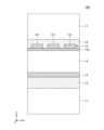
- FIG. 1B is a horizontal cross-sectional view of the frame taken along line AA in FIG. 1A. It is a figure showing an example of the layer composition of a reflective panel. It is a figure which shows another example of the layer structure of a reflective panel.
- FIG. 2 is a diagram of a conductive pattern including a unit pattern (supercell). It is a figure which shows the example of a unit pattern.
- FIG. 3 is a diagram showing an analysis space. It is a schematic diagram of the XY plane of analysis space. It is a schematic diagram of the XZ plane of analysis space.
- FIG. 3 is a diagram showing vertical polarization and horizontal polarization. It is a figure which shows the example of a structure of the metal element included in a unit pattern, and the reflection efficiency with respect to a vertically polarized wave and a horizontally polarized wave.
- a configuration that maintains the size of the supercell at the same level as before and has high sensitivity to at least one of the orthogonal polarizations is, for example, while maintaining the basic arrangement of the supercell, (a) A configuration that has a reflection efficiency of 75% or more for either vertically polarized waves or horizontally polarized waves, or (b) A configuration that has a reflection efficiency of 50% or more for both vertically polarized waves and horizontally polarized waves. , including.
- the A metal element having a longitudinal axis in the direction is divided into a plurality of segments extending in the longitudinal direction.
- the metal element included in the supercell is formed of vertical segments and horizontal segments. Specifically, one metal element is formed by at least two segments extending in the long side direction of the rectangle and at least two segments extending in the short side direction of the rectangle.
- FIG. 1A is a schematic diagram of an electromagnetic wave reflecting fence 100.
- the electromagnetic wave reflecting fence 100 includes electromagnetic wave reflecting devices 60-1, 60-2 having reflective panels 10-1, 10-2, and 10-3 (hereinafter, may be collectively referred to as "reflecting panels 10" as appropriate), and 60-3 are connected in the horizontal direction.
- the width or lateral direction of the reflective panel 10 is the X direction
- the height or vertical direction is the Y direction
- the thickness direction is the Z direction.
- an electromagnetic wave reflecting fence 100 is configured by connecting three electromagnetic wave reflecting devices 60-1, 60-2, and 60-3 (hereinafter may be collectively referred to as "electromagnetic wave reflecting device 60" as appropriate).
- electromagnetromagnetic wave reflecting device 60 there is no particular limit to the number of electromagnetic wave reflecting devices 60 that are connected.
- the reflective panels 10-1, 10-2, and 10-3 used in the electromagnetic wave reflecting devices 60-1, 60-2, and 60-3 have a frequency of 1 GHz or more and 300 GHz or less, for example, 1 GHz or more and 170 GHz or less, or 1 GHz or more and 100 GHz or less. , or reflect electromagnetic waves in a desired band selected from a frequency band of 1 GHz or more and 80 GHz or less.
- Each reflective panel 10 has a layer including a conductive pattern as a reflective film.
- the conductive pattern is designed according to the desired reflection angle, frequency band, etc.
- the reflective film may be formed with a periodic pattern, a mesh pattern, a geometric pattern, a transparent film, or the like. As described below, the conductive pattern is designed to reflect both vertically and horizontally polarized waves.
- At least a portion of the reflective panels 10-1, 10-2, and 10-3 may be non-specular reflective surfaces with different angles of incidence and reflection of electromagnetic waves.
- Non-specular reflective surfaces include diffuse surfaces, scattering surfaces, and metasurfaces that are artificial reflective surfaces designed to reflect radio waves in a desired direction. It may be desirable for the reflective panels 10-1, 10-2, and 10-3 to be electrically connected to each other from the viewpoint of maintaining continuity of reflected potential, but if they include a metasurface, adjacent There may be no electrical connection between the reflective panels 10. By holding adjacent reflective panels 10 with the frame 50, electromagnetic wave reflective fences 100 connected in the X direction can be obtained.
- the electromagnetic wave reflecting device 60 may have legs 56 that support the frame 50. As shown in FIG. 1A, when the electromagnetic wave reflecting device 60 or the electromagnetic wave reflecting fence 100 is made to stand up on an installation surface, it is desirable to provide the legs 56, but the legs 56 are not essential.
- a top frame 57 that holds the upper end of the reflective panel 10 and a bottom frame 58 that holds the lower end may be used. In this case, the frame 50, the top frame 57, and the bottom frame 58 constitute a frame that holds the entire circumference of the reflective panel 10.
- the frame 50 may also be called a "side frame" due to its positional relationship with the top frame 57 and bottom frame 58. Providing the top frame 57 and the bottom frame 58 ensures mechanical strength and safety during transportation and assembly of the reflective panel 10.
- the electromagnetic wave reflecting device 60 may be installed on a wall or ceiling by holding the reflective panel 10 with the frame 50, top frame 57, and bottom frame 58 without providing the legs 56.
- FIG. 1B shows an example of the configuration of the frame 50 along line AA in FIG. 1A in a cross-sectional view parallel to the XZ plane.
- the frame 50 has a conductive main body 500 and slits 51-1 and 51-2 formed on both sides of the main body 500 in the width direction.
- the edges of reflective panels 10-1 and 10-2 are inserted into slits 51-1 and 51-2, respectively, and held within space 52.
- the space 52 is not essential, by providing the space 52, the main body 500 of the frame 50 can be made lighter, and the holding angle of the reflective panel 10 can be made more flexible.
- Adjacent reflective panels 10-1 and 10-2 can be stably held by inserting reflective panels 10-1 and 10-2 into slits 51-1 and 51-2, respectively.
- a portion of body 500 may be formed of a non-conductive material.
- a non-conductive cover 501 made of resin or the like may be provided on the outer surface of the main body 500, but the cover 501 is not essential. When the cover 501 is provided, the cover 501 functions as a protection member that protects the frame 50.
- the reflective panel 10A includes a dielectric layer 14, a conductive pattern 15 provided on one surface of the dielectric layer 14, and a ground layer 13 provided on the opposite surface of the dielectric layer 14. , and an adhesive layer 153 supporting the conductive pattern 15 and bonding to the dielectric layer 14 .
- the conductive pattern 15 is a periodic pattern including a plurality of metal elements 151 carried in a predetermined arrangement on an adhesive layer 153.
- the dielectric layer 14 is an insulating polymer film made of polycarbonate, cycloolefin polymer (COP), polyethylene terephthalate (PET), fluororesin, etc., and has a thickness of about 0.3 mm to 1.0 mm.
- the dielectric layer 14 may be any material as long as it has a relative dielectric constant and a dielectric loss tangent suitable for realizing the target reflection characteristics.
- the reflective surface of the reflective panel 10 is formed by the conductive pattern 15 including the plurality of metal elements 151.
- the metal element 151 forming the conductive pattern 15 is made of a good conductor such as Cu, Ni, or Ag.
- the reflective surface defined by the conductive pattern 15 may include a metasurface whose reflective properties are artificially controlled.
- the conductive pattern 15 of the embodiment includes a plurality of metal elements 151 arranged in a periodic pattern, and reflects one or both of vertically polarized waves and horizontally polarized waves included in incident electromagnetic waves with high reflection efficiency. Reflect in desired direction.
- each metal Element 151 is divided into a plurality of segments extending in the longitudinal direction.
- one metal element 151 forming the periodic pattern has at least two metal elements extending in the first direction in the XY plane. and at least two segments extending in a second direction perpendicular to the first direction.
- the thickness of the metal element 151 may be set to 0.01 mm or more and 0.05 mm or less in order to maintain the flatness of the reflective surface and function sufficiently as a reflective surface.
- the occupancy rate of the conductive pattern 15 with respect to the dielectric layer 14 may be set to 5.0% or more and 30.0% or less. If transparency is not required for the reflective panel, the occupancy of the conductive pattern 15 may be set higher than 30.0% to further increase the power reflection efficiency. When transparency is required for the reflective panel 10, it is desirable to set the transmittance to visible light to 55.0% or more.
- the adhesive layer 153 is made of vinyl acetate resin, acrylic resin, cellulose resin, aniline resin, ethylene resin, silicone resin, or other resin material.
- a material having a composition satisfying a predetermined dielectric constant and dielectric loss tangent can be used as the adhesive layer 153.
- the thickness of the adhesive layer 153 is 0.002 mm or more and 0.05 mm or less, and from the viewpoint of stably holding the conductive pattern 15, it is preferably 0.01 mm or more and 0.05 mm or less.
- FIG. 3 shows an example of the configuration of the reflective panel 10B.
- the reflective panel 10B includes, in addition to the configuration shown in FIG. , and a dielectric substrate 11 connected to the ground layer 13 side by an intermediate layer 12.
- the intermediate layer 16 protects the surface of the metal element 151 of the conductive pattern 15 and also adheres and holds the dielectric substrate 17.
- the intermediate layer 16 desirably has durability and moisture resistance, and can be made of, for example, ethylene-vinyl acetate (EVA) copolymer or cycloolefin polymer (COP).
- EVA ethylene-vinyl acetate
- COP cycloolefin polymer
- the thickness of the intermediate layer 16 is 0.01 mm or more and 0.40 mm or less.
- the dielectric substrate 17 is desirably made of a material with excellent impact resistance, durability, and transparency.
- the dielectric substrate 17 polycarbonate, acrylic resin, PET, etc. can be used.
- the thickness of the dielectric substrate 17 is, for example, 1.0 mm to 10.0 mm.
- the intermediate layer 12 protects the surface of the ground layer 13 and also adheres and holds the dielectric substrate 11.
- the intermediate layer 12 desirably has durability and moisture resistance, and can be made of, for example, ethylene-vinyl acetate (EVA) copolymer or cycloolefin polymer (COP).
- EVA ethylene-vinyl acetate
- COP cycloolefin polymer
- the thickness of the intermediate layer 12 is 0.01 mm or more and 0.40 mm or less.
- the dielectric substrate 11 is desirably made of a material with excellent impact resistance, durability, and transparency.
- the dielectric substrate 11 polycarbonate, acrylic resin, PET, etc. can be used.
- the thickness of the dielectric substrate 11 is, for example, 1.0 mm to 10.0 mm.
- FIG. 4 shows an example of the conductive pattern 15 of the embodiment.
- the conductive pattern 15 is formed as a periodic pattern, and unit patterns 210 called "super cells" are repeatedly arranged in the X direction and the Y direction.
- the X direction and Y direction in FIG. 4 correspond to the X direction and Y direction of the reflective panel 10 in FIG. 1A, the X direction being the horizontal direction of the electromagnetic wave reflecting device 60, and the Y direction being the height direction.
- the unit pattern 210 includes a plurality of metal elements 151 arranged in the X direction.
- the long axis of the unit pattern 210 is parallel to the X direction.
- FIG. 5 shows an example of the metal element 151 included in the unit pattern 210.
- 5A shows a configuration that has high reflection efficiency for either polarized wave
- FIG. 5B shows a configuration that reflects both horizontally polarized waves and vertically polarized waves.
- unit patterns 210A and 210B are formed of six metal elements 151a, 151b, 151c, 151d, 151e, and 151f.
- the width W of the rectangular area occupied by each of the metal elements 151a to 151f is approximately constant, but the length L thereof is different.
- the center points of the six metal elements 151a to 151f are on the same axis, that is, on the longitudinal axis Lax of the unit pattern 210.
- the Y coordinates of the center points of metal elements 151a to 151f are constant.
- the phase of reflection is controlled by the shape and size of the metal elements 151a to 151f, and a reflected beam is formed in a desired direction by superimposing the reflected waves.
- the unit patterns 210A and 210B shown in FIG. 5 are designed so that the peak of the reflected wave of the vertically incident electromagnetic wave (incident angle 0°) appears in the direction of 50° from the normal line.
- the arrangement of unit patterns 210 is maintained as a basic arrangement.
- the configuration of the metal elements 151 included in the unit pattern 210 is variously changed, the basic arrangement as the unit pattern 210 is the same. That is, a plurality of metal elements 151 are arranged at regular intervals along the longitudinal direction (X direction) of the unit pattern 210, and the center point of each metal element 151 is on the axis Lax.
- each of the metal elements 151a to 151f is divided into two or more segments 201 extending along the long side, that is, in the Y direction.
- the size of the unit pattern 210 as a whole or the occupation rate of the metal can be increased in the Y direction perpendicular to the longitudinal axis Lax of the unit pattern 210.
- the reflection efficiency for polarized waves that vibrate can be improved.
- each of the metal elements 151a to 151f has two or more segments 201 extending in the Y direction and two or more segments 202 extending in the X direction.
- the segment 201 in the Y direction selectively reflects vertically polarized waves vibrating in a direction perpendicular to the longitudinal axis Lax of the unit pattern 210.
- the segment 202 in the X direction selectively reflects horizontally polarized waves vibrating in a direction parallel to the longitudinal axis Lax of the unit pattern 210.
- the reflective panel 10 having this configuration reflects both vertically polarized waves and horizontally polarized waves.
- Both the segment 201 extending in the Y direction and the segment 202 extending in the X direction are formed as metal wires with an aspect ratio of length to width greater than 1.
- the aspect ratio of length to width of each segment is, for example, 1.1 or more and 26.5 or less.
- FIG. 7 is a schematic diagram of the XY plane of the analytical space 101
- FIG. 8 is a schematic diagram of the XZ plane of the analytical space 101.
- the longitudinal direction of the unit pattern 210 or the short side of the metal element 151 included in the unit pattern 210 is the X direction
- the long side direction of the metal element 151 is the Y direction
- the thickness direction of the conductive pattern 15 is Let it be the Z direction.
- a model 20 of the conductive pattern 15 is arranged in the analysis space 101.
- the model 20 has an 8 ⁇ 6 unit pattern in which eight unit patterns 210 are repeatedly arranged in the X direction and six unit patterns 210 are arranged repeatedly in the Y direction.
- the boundary condition is a design in which electromagnetic wave absorbers 102 are arranged around the analysis space 101.
- the frequency of incident electromagnetic waves is set to 28.0 GHz.
- the unit pattern 210 is designed to reflect a 28 GHz vertically incident electromagnetic wave at an angle of 50°.
- the evaluation method uses a model 20 of 8 ⁇ 6 unit patterns 210 in the analysis space shown in FIGS. 6, 7, and 8.
- a plane wave of 28.0 GHz is incident on the model 20 at an incident angle of 0°, and the scattering cross section of the reflected wave is analyzed for each of vertically polarized waves and horizontally polarized waves using general-purpose three-dimensional electromagnetic field simulation software.
- the scattering cross section, or radar cross section (RCS) is used as an indicator of the ability to reflect incident electromagnetic waves.
- the power reflection efficiency of the metasurface is a value obtained by dividing the power reflection efficiency obtained from the gain value by the correction value.
- EMR is the reflected electric field on the lossless metasurface determined by the simulation model 20 in FIG. 7, and EPEC is the reflected electric field on the ideal conductive plate, then the correction value ⁇ p is set to
- ⁇ is the angle of incidence on the metasurface
- ⁇ is the corresponding angle of reflection for regular reflection.
- Figure 9 shows vertical polarization and horizontal polarization in the simulation.
- a polarized wave vibrating in the Y direction that is, in a direction parallel to the long side of the metal element 151 (see FIG. 5) constituting the unit pattern 210, is defined as a vertically polarized wave.
- polarized waves vibrating in the X direction that is, in a direction parallel to the longitudinal axis Lax of the unit pattern 210 (see FIG. 5) or in a direction parallel to the short side of the metal element 151, are horizontally polarized. Let it be a wave.
- the reflection efficiency for vertically polarized waves and horizontally polarized waves is calculated by changing the number and line width of the Y-direction segments 201 and the X-direction segments 202 (see FIG. 5) of the metal element 151 included in the unit pattern 210.
- FIG. 10 shows a configuration example of a metal element included in the unit pattern 210 and reflection efficiency for vertically polarized waves and horizontally polarized waves.
- Examples 1 to 3 correspond to configuration (a) that reflects both vertically polarized waves and horizontally polarized waves.
- a configuration that can obtain a reflection efficiency of 50% or more for both vertically polarized waves and horizontally polarized waves is a configuration that can handle both vertically polarized waves and horizontally polarized waves.
- Examples 4 to 7 correspond to the configuration (b) having high reflection efficiency for either vertically polarized waves or horizontally polarized waves.
- a configuration that has a reflection efficiency of 75% or more for either vertically polarized waves or horizontally polarized waves is defined as a configuration that has "high reflection efficiency" for either one of the polarized waves.
- the metal element 151 has two or more line segments in each of the long side direction and the short side direction, that is, two or more segments 201 in the Y direction and two or more segments 202 in the X direction.
- rectangular metal elements are formed from one solid film.
- Examples 6 and 7 have two or more line segments (segments 201 in the Y direction) extending in the long side direction, but the number of line segments (segments 202 in the X direction) in the short side direction is less than two.
- the dielectric layer 14 is made of a polycarbonate film with a thickness of 0.7 mm.
- a ground layer 13 made of an Ag-based multilayer film with a thickness of 0.36 mm is set on one side of the polycarbonate film.
- a conductive pattern 15 including unit patterns 210 each composed of metal elements 151 of different shapes is arranged on the other surface of the polycarbonate film with an adhesive layer 153 interposed therebetween.
- the material of the metal element 151 is copper foil with a thickness of 0.03 mm.
- the thickness of the adhesive layer is 0.01 mm, the relative permittivity of the adhesive layer 153 at 28.0 GHz is 2.39, and the dielectric loss tangent is 0.05.
- the length L of the six metal elements constituting the unit pattern 210 is slightly different, but this is due to the shape of the metal element 151 in each example to optimize the reflection efficiency as the unit pattern 210.
- By adjusting to A slight difference in length L due to such adjustment does not significantly affect the relationship between the reflection characteristics of vertically polarized waves and the reflection characteristics of horizontally polarized waves.
- the lengths in the long side direction of the six metal elements 151a to 151f constituting the unit pattern 210 are respectively 2.8570 mm, 2.9661 mm, 3.6795 mm, and 1.4605 mm. 2.3468mm, 2.4887mm.
- One metal element 151 has three segments 201 in the Y direction and two segments 202 in the X direction.
- the line width w1y of the segment 201 in the Y direction is 0.2 mm.
- the line width w1x of the segment 202 in the X direction is 0.1 mm, and the length is 1.6 mm.
- the aspect ratio of the length (long side) in the Y direction to the width or short side of the segment 201 in the Y direction is 11.7 or more and 18.4 or less.
- the aspect ratio of the length (long side) in the X direction to the width or short side of the segment 202 in the X direction is 16.0.
- the “aspect ratio" of the segment 201 or the segment 202 we mean the ratio of the long side to the short side of the line segments constituting each segment.
- the conductive pattern 15 having this unit pattern 210 has an occupation rate of 14.3% with respect to the dielectric layer 14, and a transmittance of visible light of 60.9%.
- the width W of the rectangular area occupied by one metal element 151 is 1.6 mm.
- a reflective panel capable of handling both vertically polarized waves and horizontally polarized waves is realized while maintaining the overall size of the unit pattern 210 to the same extent as the supercell disclosed in Non-Patent Document 1.
- the lengths in the long side direction of the six metal elements 151a to 151f constituting the unit pattern 210 are respectively 2.3612 mm, 2.6314 mm, 2.9527 mm, and 1.3072 mm. 1.6430mm, 2.1470mm.
- Each of the metal elements 151a to 151f is formed of a frame-shaped metal pattern along the outer periphery of a rectangular area. The inside of the frame-shaped pattern formed by the segments 201 in the Y direction and the segments 202 in the X direction is blank.
- the line width w2y of the segment 201 in the Y direction is 0.2 mm
- the line width w2x of the segment 202 in the X direction is 0.1 mm
- the length is 1.5 mm.
- the aspect ratio of the long side to the short side of the segment 201 in the Y direction is 8.2 or more and 14.8 or less.
- the aspect ratio of the long side to the short side of the segment 202 in the X direction is 15.0.
- the occupancy rate of the conductive pattern 15 having the unit pattern 210 with respect to the dielectric layer 14 is 8.8%, and the transmittance to visible light is 64.8%.
- Example 2 can achieve a reflection efficiency of 70% or more for vertically polarized waves and 50% or more for horizontally polarized waves while maintaining high transparency of the reflective panel. If another segment 202 in the X direction is provided between the upper and lower segments 202, it is considered that the reflection efficiency of horizontally polarized waves can be further improved without significantly increasing the occupation rate of the conductive pattern 15.
- the width W of the rectangular area occupied by one metal element 151 is 1.5 mm.
- a reflective panel capable of handling both vertically polarized waves and horizontally polarized waves is realized while maintaining the overall size of the unit pattern 210 to the same extent as the supercell disclosed in Non-Patent Document 1.
- the lengths in the long side direction of the six metal elements 151a to 151f constituting the unit pattern 210 are respectively 2.7463 mm, 2.8959 mm, 4.0117 mm, and 1.5090 mm. 2.2680mm, 2.3872mm.
- One metal element 151 has three segments 201 in the Y direction and two segments 202 in the X direction. Two X-direction segments 202 connect the upper and lower ends of three Y-direction segments 201 arranged at 0.45 mm intervals.
- the line width w3y of the segment 201 in the Y direction is 0.2 mm.
- the line width w3x of the segment 202 in the X direction is 0.1 mm, and the length is 1.5 mm.
- the aspect ratio of the long side to the short side of the segment 201 in the Y direction is 11.3 or more and 20.1 or less.
- the aspect ratio of the long side to the short side of the segment 202 in the X direction is 15.0.
- the conductive pattern 15 having this unit pattern 210 has an occupation rate of 14.1% with respect to the dielectric layer 14, and a transmittance of visible light of 61.0%.
- the width W of the rectangular area occupied by one metal element 151 is 1.5 mm.
- a reflective panel capable of handling both vertically polarized waves and horizontally polarized waves is realized while maintaining the overall size of the unit pattern 210 to the same extent as the supercell disclosed in Non-Patent Document 1.
- Example 4 is one of the configurations (a) having a reflection efficiency of 75% or more for either vertically polarized waves or horizontally polarized waves.
- each metal element 151 constituting the unit pattern 210 is formed of a rectangular solid film extending in the Y direction.
- the lengths in the long side direction of the six metal elements 151a to 151f are respectively 2.5563 mm, 2.9113 mm, 4.0717 mm, 1.2521 mm, 1.8975 mm, and 2. 5357mm.
- the width w4 of the metal elements 151a to 151f is all 1.6 mm.
- the conductive pattern 15 having this unit pattern 210 has a occupancy rate of 32.6% with respect to the dielectric layer 14 and a transmittance of visible light of 47.9%.
- each metal element 151 is formed of a rectangular solid film extending in the Y direction, so while a high reflection efficiency of over 85% is obtained for vertically polarized waves, it hardly responds to horizontally polarized waves. do not.
- This pattern can only be reflected in one polarization in systems using cross-dipole antennas or MIMO antennas that handle vertical and horizontal polarization, but it can be used effectively in systems that communicate with a single polarization. can.
- the occupancy rate of the conductive pattern 15 exceeds 30%, the transmittance for visible light is less than 50%, but it can be effectively used in application fields where transparency is not required for the reflective panel.
- each metal element 151 constituting the unit pattern 210 is formed of a narrow rectangular solid film.
- the lengths of the six metal elements 151a to 151f in the long side direction are 3.03595 mm, 3.1957 mm, 4.5762 mm, 1.8686 mm, 2.5269 mm, and 2.5 mm, respectively. 7940mm.
- the width w5 of the metal elements 151a to 151f is all 0.6 mm.
- the conductive pattern 15 having this unit pattern 210 has a high transparency, with an occupation rate of 14.4% in the dielectric layer 14 and a transmittance of visible light of 60.0%.
- the power reflection efficiency of vertically polarized waves after this is 78.2%.
- each metal element 151 is formed of a narrow rectangular solid film extending in the Y direction, a high reflection efficiency of over 75% can be obtained for vertically polarized waves, while a high reflection efficiency of over 75% can be obtained for horizontally polarized waves. does not react.
- the width in the X direction is less than half, and the transmittance to visible light is improved.
- This pattern can only be reflected in one polarization in systems using cross-dipole antennas or MIMO antennas that handle vertical and horizontal polarization, but it can be used effectively in systems that communicate with a single polarization. can. Further, it can be effectively used in an environment where transparency of the reflective panel 10 is required, such as an event venue or an office.
- Example 6 the metal element 151 constituting the unit pattern 210 is formed of three Y-direction segments 201 and does not have an X-direction segment.
- the lengths in the long side direction of the six metal elements 151a to 151f constituting the unit pattern 210 are respectively 2.8133 mm, 3.0266 mm, 4.1699 mm, and 1.4737 mm. 2.4273mm and 2.6283mm.
- the width w6 of the segment 202 in the Y direction is 0.2 mm, and the interval between adjacent segments 201 is 0.5 mm.
- the aspect ratio of the long side to the short side of the segment 201 in the Y direction is 7.4 or more and 20.8 or less.
- the aspect ratio of the long side to the short side of the segment 202 in the X direction is 16.0.
- the occupancy rate of the conductive pattern 15 having this unit pattern 210 with respect to the dielectric layer 14 is 13.3%, and the transmittance to visible light is 61.6%.
- the power reflection efficiency of vertically polarized waves is 86.0%.
- Example 6 compared to Example 4, the metal element 151 is divided into three in the X direction to form three segments 201 in the Y direction, so that the transmittance for visible light is increased and It has a reflection efficiency higher than Example 4 for waves.
- the width W of the rectangular area occupied by one metal element 151 is 1.6 mm.
- a reflective panel with high reflection efficiency and transparency for vertically polarized waves can be realized while maintaining the overall size of the unit pattern 210 to the same extent as the supercell disclosed in Non-Patent Document 1.
- Example 7 the metal element 151 constituting the unit pattern 210 has three segments 201 in the Y direction and one segment 202 in the X direction.
- the lengths in the long side direction of the six metal elements 151a to 151f constituting the unit pattern 210 are respectively 2.8705 mm, 3.1376 mm, 5.0547 mm, and 1.7671 mm. 2.3693mm, 2.6665mm.
- the line width w7y of the segment 201 in the Y direction is 0.2 mm.
- the line width w7x of the segment 202 in the X direction is 0.1 mm, and the length is 1.6 mm.
- the aspect ratio of the long side to the short side of the segment 201 in the Y direction is 8.8 or more and 25.3 or less.
- the aspect ratio of the long side to the short side of the segment 202 in the X direction is 16.0.
- the conductive pattern 15 having this unit pattern 210 has a occupancy rate of 15.5% with respect to the dielectric layer 14 and a transmittance of visible light of 60.0%.
- Example 7 With the configuration of Example 7, high reflection efficiency exceeding 85% for vertically polarized waves can be obtained while maintaining high transparency. On the other hand, having only one segment 202 in the X direction does not provide sufficient reflection efficiency for horizontally polarized waves. In this configuration, the width W of the rectangular area occupied by one metal element 151 is 1.6 mm. A reflective panel having high reflection efficiency and transparency for vertically polarized waves is realized while maintaining the overall size of the unit pattern 210 to the same extent as the supercell disclosed in Non-Patent Document 1.
- the metal element 151 included in the unit pattern 210 It is advantageous to divide the segment into two or more segments extending in a predetermined direction. By dividing one metal element 151 having a long axis in the Y direction into multiple segments 201 extending in the Y direction, the long axis of the metal element 151 can be A reflection efficiency of over 80% is obtained for polarized waves vibrating in parallel directions.
- the metal element 151 included in the unit pattern 210 is divided into two or more segments 201 in the Y direction, It is effective to form two or more X-direction segments 202.
- the reflection efficiency for vertically polarized waves and horizontally polarized waves is improved. It is desirable to appropriately design the number of divisions of the metal element in consideration of the transparency and reflection efficiency required for the reflective panel 10.
- the reflective panel of the embodiment has a simple design, maintains the basic configuration of the unit pattern 210, and can detect at least vertically polarized waves and horizontally polarized waves without significantly increasing the size of the unit pattern 210.
- high reflection efficiency can be achieved.
- vertically polarized waves can be A reflection efficiency of 50% or more can be achieved for each horizontally polarized wave.
- the reflective panel of the embodiment is not limited to the configuration example described above.
- a segment 202 extending in the X direction may be added at the center in the Y direction to use three segments 202.
- the upper and lower segments 202 may be arranged symmetrically with respect to the third segment 202 in the X direction.
- two segments 202 may be added above and below the segment 202 in the X direction.
- the solid film of Example 4 or Example 5 may be divided in the X direction to form two or more segments extending in the Y direction. The divided segments may be connected by two or more segments in the X direction.
- the reflection angle with respect to normal incidence can be appropriately designed in the range of 5° or more and less than 90°. can do.
- the in-plane size of the reflective panel 10 can be appropriately selected from a range of 30 cm x 30 cm to 3 m x 3 m.
- the entire surface of the reflective panel 10 may be a metasurface, or a portion may be a specular reflective surface.
- the present disclosure may include the following configurations.
- (Section 1) a dielectric layer; a periodic conductive pattern provided on the surface of the dielectric layer; has The periodic conductive pattern is a repeating unit pattern in which metal elements having long axes in a first direction within the plane of the dielectric layer are arranged at predetermined intervals in a second direction perpendicular to the first direction. including; The metal element is formed of two or more first segments that are divided in the second direction and extend in the first direction.
- reflective panel (Section 2) The metal element has two or more first segments and two or more second segments extending in the second direction. Item 1. The reflective panel according to item 1.
- the second segment connects ends of two or more of the first segments; Item 2. Reflective panel according to item 2.
- the second segment is provided symmetrically with respect to the longitudinal center of the two or more first segments, Item 2. Reflective panel according to item 2.
- an aspect ratio of the length of the first segment in the first direction to the width of the first segment is greater than 1 and less than or equal to 26.5; Item 5.
- the reflective panel according to any one of Items 1 to 4. The occupancy rate of the conductive pattern with respect to the dielectric layer is 5.0% or more and 30.0% or less, Item 5.
- the transmittance of the reflective panel to visible light is 55.0% or more.
- Item 7. The reflective panel according to any one of Items 1 to 6.
- the periodic conductive pattern is supported on the dielectric layer via an adhesive layer, Item 8.
- the reflective panel according to any one of Items 1 to 7. (Section 9) The reflective panel according to any one of Items 1 to 8, which reflects radio waves in a desired band selected from a frequency band of 1 GHz or more and 300 GHz or less; a frame holding the reflective panel; An electromagnetic wave reflecting device. (Section 10) 10.
- An electromagnetic wave reflecting fence comprising two or more electromagnetic wave reflecting devices according to Item 9, and two or more of the reflecting panels connected by the frame.
Landscapes
- Physics & Mathematics (AREA)
- Electromagnetism (AREA)
- Aerials With Secondary Devices (AREA)
Priority Applications (1)
| Application Number | Priority Date | Filing Date | Title |
|---|---|---|---|
| JP2024538931A JPWO2024029365A1 (https=) | 2022-08-05 | 2023-07-20 |
Applications Claiming Priority (2)
| Application Number | Priority Date | Filing Date | Title |
|---|---|---|---|
| JP2022125798 | 2022-08-05 | ||
| JP2022-125798 | 2022-08-05 |
Publications (1)
| Publication Number | Publication Date |
|---|---|
| WO2024029365A1 true WO2024029365A1 (ja) | 2024-02-08 |
Family
ID=89848907
Family Applications (1)
| Application Number | Title | Priority Date | Filing Date |
|---|---|---|---|
| PCT/JP2023/026671 Ceased WO2024029365A1 (ja) | 2022-08-05 | 2023-07-20 | 反射パネル、これを用いた電磁波反射装置、及び電磁波反射フェンス |
Country Status (3)
| Country | Link |
|---|---|
| JP (1) | JPWO2024029365A1 (https=) |
| TW (1) | TW202410552A (https=) |
| WO (1) | WO2024029365A1 (https=) |
Citations (4)
| Publication number | Priority date | Publication date | Assignee | Title |
|---|---|---|---|---|
| JP2011019021A (ja) * | 2009-07-07 | 2011-01-27 | Ntt Docomo Inc | リフレクトアレイ |
| CN107394318A (zh) * | 2017-07-14 | 2017-11-24 | 合肥工业大学 | 一种用于反射式可调移相器的液晶移相单元 |
| WO2021199503A1 (ja) * | 2020-03-31 | 2021-10-07 | Agc株式会社 | 電磁波反射装置、電磁波反射フェンス、及び電磁波反射装置の組み立て方法 |
| WO2022163813A1 (ja) * | 2021-01-29 | 2022-08-04 | 積水化学工業株式会社 | 構造体、及び建築材料 |
-
2023
- 2023-07-20 JP JP2024538931A patent/JPWO2024029365A1/ja active Pending
- 2023-07-20 WO PCT/JP2023/026671 patent/WO2024029365A1/ja not_active Ceased
- 2023-07-25 TW TW112127714A patent/TW202410552A/zh unknown
Patent Citations (4)
| Publication number | Priority date | Publication date | Assignee | Title |
|---|---|---|---|---|
| JP2011019021A (ja) * | 2009-07-07 | 2011-01-27 | Ntt Docomo Inc | リフレクトアレイ |
| CN107394318A (zh) * | 2017-07-14 | 2017-11-24 | 合肥工业大学 | 一种用于反射式可调移相器的液晶移相单元 |
| WO2021199503A1 (ja) * | 2020-03-31 | 2021-10-07 | Agc株式会社 | 電磁波反射装置、電磁波反射フェンス、及び電磁波反射装置の組み立て方法 |
| WO2022163813A1 (ja) * | 2021-01-29 | 2022-08-04 | 積水化学工業株式会社 | 構造体、及び建築材料 |
Also Published As
| Publication number | Publication date |
|---|---|
| TW202410552A (zh) | 2024-03-01 |
| JPWO2024029365A1 (https=) | 2024-02-08 |
Similar Documents
| Publication | Publication Date | Title |
|---|---|---|
| US8164506B2 (en) | Electromagnetic absorber using resistive material | |
| US20250174903A1 (en) | Frequency-selective reflecting plate and communication relay system | |
| US20250055201A1 (en) | Electromagnetic wave reflecting device, electromagnetic wave reflecting fence, and reflection panel | |
| CN106415928A (zh) | 天线 | |
| CN208460991U (zh) | 一种基于风车结构的平面反射阵列天线 | |
| KR20230085178A (ko) | 반사어레이 및 이를 위한 방법 | |
| US20250096480A1 (en) | Electromagnetic wave reflecting device, electromagnetic wave reflecting fence, and reflection panel | |
| TW202425422A (zh) | 反射板、使用其之電磁波反射裝置及電磁波反射柵 | |
| WO2023218887A1 (ja) | 電磁波反射装置、及び電磁波反射フェンス | |
| EP1900114A1 (en) | A passive repeater antenna | |
| WO2023120471A1 (ja) | 電波集束体、窓ガラス、及び、電波通信システム | |
| WO2024029365A1 (ja) | 反射パネル、これを用いた電磁波反射装置、及び電磁波反射フェンス | |
| WO2023003961A1 (en) | Method and system with fragmented metastructures formed with a plurality of metasurface arrays | |
| JP7673754B2 (ja) | アンテナセット | |
| WO2025158773A1 (ja) | 電磁波反射パネル、電磁波反射装置、及び電磁波反射フェンス | |
| WO2024241665A1 (ja) | 電磁波反射パネル、電磁波反射装置、及び電磁波反射フェンス | |
| WO2024106405A1 (ja) | 電波反射体、電波反射体の作製方法、電波反射構造体、電波反射システムおよび電波反射装置 | |
| WO2023233885A1 (ja) | 電磁波反射装置、電磁波反射フェンス、及び反射パネル | |
| WO2023233921A1 (ja) | 電磁波反射装置、電磁波反射フェンス、及び反射パネル | |
| CN114566811A (zh) | 一种模块化可拼接高环境适应性天线子阵 | |
| CN102723580B (zh) | 一种便携式超材料卫星天线及卫星接收系统 | |
| WO2024135216A1 (ja) | 反射パネル、電磁波反射装置、及び電磁波反射フェンス | |
| JP2026054790A (ja) | 電波反射体および反射鏡アンテナ | |
| US20250309555A1 (en) | Reflection panel and electromagnetic-wave reflecting apparatus | |
| JP2013175800A (ja) | レーダ反射器 |
Legal Events
| Date | Code | Title | Description |
|---|---|---|---|
| 121 | Ep: the epo has been informed by wipo that ep was designated in this application |
Ref document number: 23849920 Country of ref document: EP Kind code of ref document: A1 |
|
| WWE | Wipo information: entry into national phase |
Ref document number: 2024538931 Country of ref document: JP |
|
| NENP | Non-entry into the national phase |
Ref country code: DE |
|
| 122 | Ep: pct application non-entry in european phase |
Ref document number: 23849920 Country of ref document: EP Kind code of ref document: A1 |