WO2024029170A1 - 電波反射装置の検査方法 - Google Patents
電波反射装置の検査方法 Download PDFInfo
- Publication number
- WO2024029170A1 WO2024029170A1 PCT/JP2023/019428 JP2023019428W WO2024029170A1 WO 2024029170 A1 WO2024029170 A1 WO 2024029170A1 JP 2023019428 W JP2023019428 W JP 2023019428W WO 2024029170 A1 WO2024029170 A1 WO 2024029170A1
- Authority
- WO
- WIPO (PCT)
- Prior art keywords
- voltage
- radio wave
- frame
- width
- common electrode
- Prior art date
- Legal status (The legal status is an assumption and is not a legal conclusion. Google has not performed a legal analysis and makes no representation as to the accuracy of the status listed.)
- Ceased
Links
Images

















Classifications
-
- G—PHYSICS
- G01—MEASURING; TESTING
- G01R—MEASURING ELECTRIC VARIABLES; MEASURING MAGNETIC VARIABLES
- G01R29/00—Arrangements for measuring or indicating electric quantities not covered by groups G01R19/00 - G01R27/00
- G01R29/08—Measuring electromagnetic field characteristics
- G01R29/0864—Measuring electromagnetic field characteristics characterised by constructional or functional features
- G01R29/0871—Complete apparatus or systems; circuits, e.g. receivers or amplifiers
-
- G—PHYSICS
- G02—OPTICS
- G02F—OPTICAL DEVICES OR ARRANGEMENTS FOR THE CONTROL OF LIGHT BY MODIFICATION OF THE OPTICAL PROPERTIES OF THE MEDIA OF THE ELEMENTS INVOLVED THEREIN; NON-LINEAR OPTICS; FREQUENCY-CHANGING OF LIGHT; OPTICAL LOGIC ELEMENTS; OPTICAL ANALOGUE/DIGITAL CONVERTERS
- G02F1/00—Devices or arrangements for the control of the intensity, colour, phase, polarisation or direction of light arriving from an independent light source, e.g. switching, gating or modulating; Non-linear optics
- G02F1/01—Devices or arrangements for the control of the intensity, colour, phase, polarisation or direction of light arriving from an independent light source, e.g. switching, gating or modulating; Non-linear optics for the control of the intensity, phase, polarisation or colour
- G02F1/13—Devices or arrangements for the control of the intensity, colour, phase, polarisation or direction of light arriving from an independent light source, e.g. switching, gating or modulating; Non-linear optics for the control of the intensity, phase, polarisation or colour based on liquid crystals, e.g. single liquid crystal display cells
- G02F1/1306—Details
- G02F1/1309—Repairing; Testing
-
- H—ELECTRICITY
- H01—ELECTRIC ELEMENTS
- H01P—WAVEGUIDES; RESONATORS, LINES, OR OTHER DEVICES OF THE WAVEGUIDE TYPE
- H01P1/00—Auxiliary devices
- H01P1/18—Phase-shifters
-
- H—ELECTRICITY
- H01—ELECTRIC ELEMENTS
- H01Q—ANTENNAS, i.e. RADIO AERIALS
- H01Q15/00—Devices for reflection, refraction, diffraction or polarisation of waves radiated from an antenna, e.g. quasi-optical devices
- H01Q15/14—Reflecting surfaces; Equivalent structures
-
- H—ELECTRICITY
- H01—ELECTRIC ELEMENTS
- H01Q—ANTENNAS, i.e. RADIO AERIALS
- H01Q3/00—Arrangements for changing or varying the orientation or the shape of the directional pattern of the waves radiated from an antenna or antenna system
- H01Q3/26—Arrangements for changing or varying the orientation or the shape of the directional pattern of the waves radiated from an antenna or antenna system varying the relative phase or relative amplitude of energisation between two or more active radiating elements; varying the distribution of energy across a radiating aperture
- H01Q3/30—Arrangements for changing or varying the orientation or the shape of the directional pattern of the waves radiated from an antenna or antenna system varying the relative phase or relative amplitude of energisation between two or more active radiating elements; varying the distribution of energy across a radiating aperture varying the relative phase between the radiating elements of an array
- H01Q3/34—Arrangements for changing or varying the orientation or the shape of the directional pattern of the waves radiated from an antenna or antenna system varying the relative phase or relative amplitude of energisation between two or more active radiating elements; varying the distribution of energy across a radiating aperture varying the relative phase between the radiating elements of an array by electrical means
- H01Q3/36—Arrangements for changing or varying the orientation or the shape of the directional pattern of the waves radiated from an antenna or antenna system varying the relative phase or relative amplitude of energisation between two or more active radiating elements; varying the distribution of energy across a radiating aperture varying the relative phase between the radiating elements of an array by electrical means with variable phase-shifters
-
- G—PHYSICS
- G02—OPTICS
- G02F—OPTICAL DEVICES OR ARRANGEMENTS FOR THE CONTROL OF LIGHT BY MODIFICATION OF THE OPTICAL PROPERTIES OF THE MEDIA OF THE ELEMENTS INVOLVED THEREIN; NON-LINEAR OPTICS; FREQUENCY-CHANGING OF LIGHT; OPTICAL LOGIC ELEMENTS; OPTICAL ANALOGUE/DIGITAL CONVERTERS
- G02F2203/00—Function characteristic
- G02F2203/02—Function characteristic reflective
Definitions
- the present invention relates to a method for inspecting a radio wave reflecting device.
- a phased array antenna device controls the directivity of a fixed antenna by adjusting the amplitude and phase of a high-frequency signal applied to each of a plurality of antenna elements arranged in a planar manner. ing. Phased array antenna devices require a phase shifter. A phased array antenna device using a phase shifter that utilizes a change in dielectric constant depending on the alignment state of liquid crystal has been disclosed (see, for example, Patent Document 1 and Patent Document 2).
- radio wave reflecting devices using liquid crystals have a problem in that there is no way to judge whether the device is good or bad by observing a reflecting element that cannot control desired radio waves.
- radio wave reflecting devices unlike display devices that use transparent electrodes as pixel electrodes, radio wave reflecting devices often use light-shielding metal for patch electrodes, which limits the area in which the inside of the radio wave reflecting device can be directly observed non-destructively. There was a problem with this.
- a method for inspecting a radio wave reflecting device is a method for inspecting a radio wave reflecting device having a plurality of reflecting elements arranged in a row direction and a column direction, wherein each of the plurality of reflecting elements has a patch electrode. , a common electrode overlapping the back side of the patch electrode, and a liquid crystal layer between the patch electrode and the common electrode, and a voltage V1 is applied between each of the plurality of patch electrodes and the common electrode.
- V1 is applied between each of the plurality of patch electrodes and the common electrode.
- 1 is a plan view of a reflection element used in a radio wave reflection device according to an embodiment of the present invention.
- 1 shows a cross-sectional view of a reflection element used in a radio wave reflection device according to an embodiment of the present invention.
- 2 shows a state in which a reflecting element used in a radio wave reflecting device according to an embodiment of the present invention operates, and shows a state in which no voltage is applied between a patch electrode and a common electrode.
- 1 shows a state in which a reflecting element used in a radio wave reflecting device according to an embodiment of the present invention operates, and shows a state in which a voltage is applied between a patch electrode and a common electrode.
- 1 shows a configuration of a radio wave reflecting device according to an embodiment of the present invention.
- FIG. 2 schematically shows that the traveling direction of reflected waves changes by the radio wave reflecting device according to an embodiment of the present invention.
- 1 shows a configuration of a radio wave reflecting device according to an embodiment of the present invention.
- 1 shows a cross-sectional view of a reflecting element in a radio wave reflecting device according to an embodiment of the present invention.
- FIG. 2 is a plan view for explaining a method for inspecting a radio wave reflecting device according to an embodiment of the present invention.
- FIG. 2 is a plan view for explaining a method for inspecting a radio wave reflecting device according to an embodiment of the present invention.
- FIG. 2 is a plan view for explaining a method for inspecting a radio wave reflecting device according to an embodiment of the present invention.
- FIG. 2 is a plan view for explaining a method for inspecting a radio wave reflecting device according to an embodiment of the present invention.
- FIG. 2 is a plan view for explaining a method for inspecting a radio wave reflecting device according to an embodiment of the present invention.
- FIG. 2 is a cross-sectional view for explaining a method for inspecting a radio wave reflecting device according to an embodiment of the present invention.
- FIG. 2 is a cross-sectional view for explaining a method for inspecting a radio wave reflecting device according to an embodiment of the present invention.
- FIG. 2 is a cross-sectional view for explaining a method for inspecting a radio wave reflecting device according to an embodiment of the present invention.
- FIG. 2 is a plan view for explaining a method for inspecting a radio wave reflecting device according to an embodiment of the present invention.
- FIG. 2 is a plan view for explaining a method for inspecting a radio wave reflecting device according to an embodiment of the present invention.
- FIG. 2 is a plan view for explaining a method for inspecting a radio wave reflecting device according to an embodiment of the present invention.
- FIG. 2 is a cross-sectional view for explaining a method for inspecting a radio wave reflecting device according to an embodiment of the present invention.
- FIG. 2 is a cross-sectional view for explaining a method for inspecting a radio wave reflecting device according to an embodiment of the present invention.
- FIG. 2 is a cross-sectional view for explaining a method for inspecting a radio wave reflecting device according to an embodiment of the present invention.
- FIG. 2 is a plan view for explaining a method for inspecting a radio wave reflecting device according to an embodiment of the present invention.
- FIG. 2 is a plan view for explaining a method for inspecting a radio wave reflecting device according to an embodiment of the present invention.
- FIG. 2 is a plan view for explaining a method for inspecting a radio wave reflecting device according to an embodiment of the present invention.
- FIG. 2 is a cross-sectional view for explaining a method for inspecting a radio wave reflecting device according to an embodiment of the present invention.
- FIG. 2 is a cross-sectional view for explaining a method for inspecting a radio wave reflecting device according to an embodiment of the present invention.
- FIG. 2 is a cross-sectional view for explaining a method for inspecting a radio wave reflecting device according to an embodiment of the present invention.
- FIG. 2 is a plan view for explaining a method for inspecting a radio wave reflecting device according to an embodiment of the present invention.
- FIG. 2 is a plan view for explaining a method for inspecting a radio wave reflecting device according to an embodiment of the present invention.
- FIG. 2 is a plan view for explaining a method for inspecting a radio wave reflecting device according to an embodiment of the present invention.
- FIG. 2 is a cross-sectional view for explaining a method for inspecting a radio wave reflecting device according to an embodiment of the present invention.
- FIG. 2 is a cross-sectional view for explaining a method for inspecting a radio wave reflecting device according to an embodiment of the present invention.
- FIG. 2 is a cross-sectional view for explaining a method for inspecting a radio wave reflecting device according to an embodiment of the present invention.
- FIG. 2 is a plan view for explaining a method for inspecting a radio wave reflecting device according to an embodiment of the present invention.
- a member or region when a member or region is said to be “above (or below)" another member or region, it means that it is directly above (or directly below) the other member or region unless otherwise specified. This includes not only the case where the item is located above (or below) another member or area, that is, the case where another component is included in between above (or below) the other member or area. .
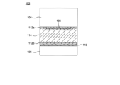
- FIGS. 1A and 1B show a reflection element 102 used in a radio wave reflection device 100 according to an embodiment of the present invention.
- FIG. 1A shows a plan view of the reflective element 102 viewed from above (the side where radio waves are incident), and
- FIG. 1B shows a cross-sectional view along A1-A2 shown in the plan view.
- the reflective element 102 includes a dielectric substrate 104, a counter substrate 106, a patch electrode 108, a common electrode 110, a first alignment film 112a, a second alignment film 112b, and a liquid crystal layer 114.
- the dielectric substrate 104 in the reflective element 102 can also be considered as a dielectric layer, forming one layer.
- Patch electrode 108 is provided on dielectric substrate (dielectric layer) 104, and common electrode 110 is provided on counter substrate 106.
- Common electrode 110 is arranged on the back side of patch electrode 108.
- a first alignment film 112a is provided on the dielectric substrate (dielectric layer) 104 so as to cover the patch electrode 108, and a second alignment film 112b is provided on the counter substrate 106 so as to cover the common electrode 110.
- Patch electrode 108 and common electrode 110 are arranged to face each other, and a liquid crystal layer 114 is provided between them.
- a first alignment film 112a is interposed between the patch electrode 108 and the liquid crystal layer 114, and a second alignment film 112b is interposed between the common electrode 110 and the liquid crystal layer 114.
- the patch electrode 108 preferably has a shape that is symmetrical with respect to vertically polarized waves and horizontally polarized waves of incident radio waves, and has a square or circular shape in plan view.
- FIG. 1A shows a case where the patch electrode 108 is square in plan view.
- the shape of the common electrode 110 is not particularly limited, and has a shape that extends over substantially the entire surface of the counter substrate 106 so as to have a larger area than the patch electrode 108.
- a first wiring 118 may be provided on the dielectric substrate (dielectric layer) 104. First wiring 118 is connected to patch electrode 108 . The first wiring 118 can be used when applying a control signal to the patch electrode 108. Furthermore, when a plurality of reflective elements are arranged, the first wiring 118 can be used to connect one patch electrode to an adjacent patch electrode.
- the dielectric substrate (dielectric layer) 104 and the counter substrate 106 are bonded together using a sealing material.
- the dielectric substrate (dielectric layer) 104 and the counter substrate 106 are arranged to face each other with a gap therebetween, and the liquid crystal layer 114 is provided in a region surrounded by a sealant.
- the liquid crystal layer 114 is provided so as to fill the gap between the dielectric substrate (dielectric layer) 104 and the counter substrate 106 .
- the distance between the dielectric substrate (dielectric layer) 104 and the counter substrate 106 is 20 to 100 ⁇ m, for example, 50 ⁇ m.
- a patch electrode 108, a common electrode 110, a first alignment film 112a, and a second alignment film 112b are provided between the dielectric substrate (dielectric layer) 104 and the counter substrate 106, so to be more precise, the dielectric substrate 104
- the thickness of the liquid crystal layer 114 is the distance between the first alignment film 112a and the second alignment film 112b provided on each of the opposing substrates 106 and 106.
- a spacer may be provided between the dielectric substrate (dielectric layer) 104 and the counter substrate 106 in order to keep the distance constant.
- a control signal for controlling the orientation of liquid crystal molecules in the liquid crystal layer 114 is applied to the patch electrode 108.
- the control signal is a DC voltage signal or a polarity inversion signal in which a positive DC voltage and a negative DC voltage are alternately inverted.
- the common electrode 110 is applied with a voltage at an intermediate level of ground or a polarity inverted signal.
- a liquid crystal material having dielectric anisotropy is used for the liquid crystal layer 114.
- the liquid crystal layer 114 nematic liquid crystal, smectic liquid crystal, cholesteric liquid crystal, or discotic liquid crystal can be used.
- the dielectric constant of the liquid crystal layer 114 having dielectric anisotropy changes due to changes in the alignment state of liquid crystal molecules.
- the reflective element 102 can change the dielectric constant of the liquid crystal layer 114 according to a control signal applied to the patch electrode 108, thereby delaying the phase of the reflected wave when reflecting the radio wave.
- the frequency bands of the radio waves reflected by the reflective element 102 are a very high frequency (VHF) band, an ultra-high frequency (UHF) band, and a microwave (SHF: super high frequency) band. , submillimeter wave (THF: These are the extremely high frequency (tremendously high frequency) and millimeter wave (EHF: extra high frequency) bands.
- VHF very high frequency
- UHF ultra-high frequency
- SHF microwave
- SHF super high frequency
- THF submillimeter wave
- EHF extra high frequency
- FIG. 2A shows a state in which no voltage is applied between the patch electrode 108 and the common electrode 110 (referred to as a "first state").
- FIG. 2A shows a case where the first alignment film 112a and the second alignment film 112b are horizontal alignment films. The long axes of the liquid crystal molecules 116 in the first state are aligned horizontally with respect to the surfaces of the patch electrode 108 and the common electrode 110 by the first alignment film 112a and the second alignment film 112b.
- FIG. 2B shows a state in which a control signal (voltage signal) is applied to the patch electrode 108 (referred to as a "second state").
- the long axes of the liquid crystal molecules 116 are aligned perpendicular to the surfaces of the patch electrode 108 and the common electrode 110 under the action of the electric field.
- the angle at which the long axes of the liquid crystal molecules 116 are oriented is determined by the magnitude of the control signal applied to the patch electrode 108 (the magnitude of the voltage between the counter electrode and the patch electrode), so that the liquid crystal molecules 116 are oriented in a direction intermediate between the horizontal direction and the vertical direction. You can also do that.
- the dielectric constant is larger in the second state than in the first state. Further, when the liquid crystal molecules 116 have negative dielectric anisotropy, the apparent dielectric constant in the second state is smaller than that in the first state.
- the liquid crystal layer 114 having dielectric anisotropy can also be regarded as a variable dielectric layer.
- the reflective element 102 can be controlled to delay (or not delay) the phase of the reflected wave by utilizing the dielectric anisotropy of the liquid crystal layer 114.
- the reflecting element 102 is used as a radio wave reflecting plate that reflects radio waves in a predetermined direction. It is preferable that the reflection element 102 attenuates the amplitude of reflected radio waves as little as possible. As is clear from the structure shown in FIG. 1B, when a radio wave propagating in the air is reflected by the reflecting element 102, the radio wave passes through the dielectric substrate (dielectric layer) 104 twice.
- the dielectric substrate (dielectric layer) 104 is made of, for example, a dielectric material such as glass or resin.
- Radio Wave Reflector Next, the configuration of a radio wave reflector in which reflective elements are integrated will be shown.
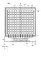
- FIG. 3 shows the configuration of a radio wave reflecting device 100a according to an embodiment of the present invention.
- the radio wave reflection device 100 has a radio wave reflection plate 120.
- the radio wave reflecting plate 120 is composed of a plurality of reflecting elements 102.
- the plurality of reflective elements 102 are arranged, for example, in a column direction (X-axis direction shown in FIG. 3) and a row direction (Y-axis direction shown in FIG. 3) intersecting the column direction.
- the reflective element 102 is arranged so that the patch electrode 108 faces the radio wave incident surface.
- the radio wave reflecting plate 120 has a flat plate shape, and a plurality of patch electrodes 108 are arranged in a matrix within the plane of this flat plate.
- the radio wave reflecting device 100a has a structure in which a plurality of reflecting elements 102 are integrated on one dielectric substrate (dielectric layer) 104.
- the radio wave reflection device 100 includes a dielectric substrate (dielectric layer) 104 on which a plurality of patch electrodes 108 are arranged, and a counter substrate 106 on which a common electrode 110 is provided, which are arranged one on top of the other. It has a structure in which a liquid crystal layer (not shown) is provided between two substrates.
- the radio wave reflecting plate 120 is formed in a region where the plurality of patch electrodes 108 and the common electrode 110 overlap.
- the cross-sectional structure of the radio wave reflecting plate 120 is the same as the structure of the reflecting element 102 shown in FIG.
- the dielectric substrate (dielectric layer) 104 and the counter substrate 106 are bonded together with a sealant 128, and a liquid crystal layer (not shown) is provided in an area inside the sealant 128.
- the dielectric substrate (dielectric layer) 104 has a peripheral region 122 that extends outward from the counter substrate 106 in addition to a region facing the counter substrate 106 .
- a first drive circuit 124 and a terminal section 126 are provided in the peripheral region 122.
- the first drive circuit 124 outputs a control signal to the patch electrode 108.
- the terminal portion 126 is a region for forming a connection with an external circuit, and is connected to, for example, a flexible printed circuit board (not shown).
- a signal for controlling the first drive circuit 124 is input to the terminal section 126 .
- a plurality of patch electrodes 108 are arranged on the dielectric substrate (dielectric layer) 104 in the column direction (X-axis direction) and the row direction (Y-axis direction). Further, a plurality of first wirings 118 extending in the row direction (Y-axis direction) are arranged on the dielectric substrate (dielectric layer) 104. Each of the plurality of first wirings 118 is electrically connected to the plurality of patch electrodes 108 arranged in the row direction (Y-axis direction). In other words, the plurality of patch electrodes 108 arranged in the row direction (Y-axis direction) are connected by the first wiring 118.
- the radio wave reflecting plate 120 has a configuration in which a plurality of patch electrode arrays are arranged in a column direction (X-axis direction) and connected by first wiring 118.
- a plurality of first wirings 118 arranged on the radio wave reflecting plate 120 extend to the peripheral region 122 and are connected to the first drive circuit 124.
- the first drive circuit 124 can output control signals of different voltage levels to each of the plurality of first wirings 118.
- a control signal is applied to each patch electrode 108).
- a control signal is applied to each set of a plurality of patch electrodes 108 arranged in the row direction (Y-axis direction), thereby controlling the direction of reflection of the reflected radio waves incident on the radio wave reflection plate 120.
- the radio wave reflecting device 100a can control the propagation direction of the reflected waves in the left-right direction of the drawing with the reflection axis VR parallel to the row direction (Y-axis direction) as the center of the radio waves irradiated to the radio wave reflection plate 120. can.
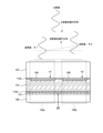
- FIG. 4 schematically shows that the traveling direction of the reflected wave changes due to the two reflecting elements 102.
- V1 ⁇ V2 different control signals
- the reflection direction can be controlled in a uniaxial direction.
- Radio wave reflection device B (two-axis reflection control) Since the radio wave reflection device 100a shown in FIG. 3 has a single reflection axis VR, it is possible to control the reflection angle in a direction with the reflection axis VR as the rotation axis. In contrast, this embodiment shows an example of a radio wave reflection device 100b that can perform biaxial reflection control. In the following description, the explanation will focus on parts that are different from the radio wave reflecting device 100a.
- the radio wave reflection device 100b has a plurality of second wirings 132 extending in the column direction (X-axis direction).
- the plurality of first wirings 118 and the plurality of second wirings 132 are arranged to intersect with each other with an insulating layer (not shown) in between.
- the plurality of first wirings 118 are connected to the first drive circuit 124, and the plurality of second wirings 132 are connected to the second drive circuit 130.
- the second drive circuit 130 outputs a scanning signal.
- FIG. 5 shows an enlarged inset view of the arrangement of the four patch electrodes 108, the two first wirings 118, and the second wirings 132.
- Each of the four patch electrodes 108 is provided with a switching element 134. Switching (on and off) of the switching element 134 is controlled by a scanning signal applied to the second wiring 132.
- the patch electrode 108 with the switching element 134 turned on is electrically connected to the first wiring 118 and a control signal is applied thereto.
- the switching element 134 is formed of, for example, a thin film transistor. According to such a configuration, a plurality of patch electrodes 108 arranged in the column direction (X-axis direction) can be selected for each row, and control signals of different voltage levels can be applied to each row.
- the radio wave reflecting device 100b shown in FIG. 5 controls the propagation direction of the reflected waves in the horizontal direction of the drawing with the radio waves irradiated on the radio wave reflecting plate 120 centered on the reflection axis VR parallel to the row direction (Y-axis direction). In addition to this, it is also possible to control the traveling direction of reflected waves in the vertical direction of the drawing centering on the reflection axis HR parallel to the row direction (X-axis direction).
- the radio wave reflection device 100b has a reflection axis VR parallel to the row direction (Y-axis direction) and a reflection axis HR parallel to the column direction (X-axis direction), the direction with the reflection axis VR as the rotation axis,
- the reflection angle can be controlled in the direction with the reflection axis HR as the rotation axis.
- the reflection direction can be changed to the uniaxial direction and the biaxial direction. can be controlled.
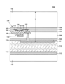
- FIG. 6 shows an example of the cross-sectional structure of the reflective element 102 in which the switching element 134 is connected to the patch electrode 108.
- a switching element 134 is provided on the dielectric substrate (dielectric layer) 104.
- the switching element 134 is a transistor, and has a structure in which a first gate electrode 138, a first gate insulating layer 140, a semiconductor layer 142, a second gate insulating layer 146, and a second gate electrode 148 are stacked.
- An undercoat layer 136 may be provided between the first gate electrode 138 and the dielectric substrate (dielectric layer) 104.
- a first wiring 118 is provided between the first gate insulating layer 140 and the second gate insulating layer 146.
- the first wiring 118 is provided so as to be in contact with the semiconductor layer 142. Further, the first connection wiring 144 is provided in the same layer as the conductive layer forming the first wiring 118. The first connection wiring 144 is provided so as to be in contact with the semiconductor layer 142.
- the connection structure of the first wiring 118 and the first connection wiring 144 to the semiconductor layer 142 shows a structure in which one wiring is connected to the source of the transistor and the other wiring is connected to the drain.
- a first interlayer insulating layer 150 is provided to cover the switching element 134.
- a second wiring 132 is provided on the first interlayer insulating layer 150.
- the second wiring 132 is connected to the second gate electrode 148 through a contact hole formed in the first interlayer insulating layer 150.
- the first gate electrode 138 and the second gate electrode 148 are electrically connected to each other in a region that does not overlap with the semiconductor layer 142.
- a second connection wiring 152 is provided on the first interlayer insulating layer 150 using the same conductive layer as the second wiring 132 .
- the second connection wiring 152 is connected to the first connection wiring 144 through a contact hole formed in the first interlayer insulating layer 150.
- a second interlayer insulating layer 154 is provided to cover the second wiring 132 and the second connection wiring 152. Further, a flattening layer 156 is provided to fill the difference in level of the switching element 134. By providing the planarizing layer 156, the patch electrode 108 can be formed without being affected by the arrangement of the switching elements 134.
- a passivation layer 158 is provided on the planar surface of planarization layer 156. Patch electrode 108 is provided on passivation layer 158. The patch electrode 108 is connected to the second connection wiring 152 through a contact hole penetrating the passivation layer 158, the planarization layer 156, and the second interlayer insulating layer 154.
- a first alignment film 112a is provided on the patch electrode 108.
- the counter substrate 106 is provided with a common electrode 110 and a second alignment film 112b, as in FIG. 1B.
- the surface of the dielectric substrate (dielectric layer) 104 on which the switching element 134 and patch electrode 108 are provided is arranged so as to face the surface of the counter substrate on which the common electrode 110 is provided, and the liquid crystal layer 114 is provided between them.
- the thickness T of the dielectric substrate (dielectric layer) 104 is from the surface of the patch electrode 108 on the liquid crystal layer 114 side to the surface of the dielectric substrate (dielectric layer) 104 opposite to the surface on which the patch electrode 108 is provided.
- the length can be as follows.
- At least one insulating layer (undercoat layer 136, first gate insulating layer 140, second gate insulating layer 146, first interlayer
- the thicknesses of the insulating layer 150, the second interlayer insulating layer 154, the planarization layer 156, and the passivation layer 158) can be taken into account.
- the undercoat layer 136 is formed of, for example, a silicon oxide film.
- the first gate insulating layer 140 and the second gate insulating layer 146 are formed of, for example, a silicon oxide film or a laminated structure of a silicon oxide film and a silicon nitride film.
- the semiconductor layer is formed of a silicon semiconductor such as amorphous silicon or polycrystalline silicon, or an oxide semiconductor containing a metal oxide such as indium oxide, zinc oxide, or gallium oxide.
- the first gate electrode 138 and the second gate electrode 148 may be made of, for example, molybdenum (Mo), tungsten (W), or an alloy thereof.
- the first wiring 118, the second wiring 132, the first connection wiring 144, and the second connection wiring 152 are formed using a metal material such as titanium (Ti), aluminum (Al), or molybdenum (Mo).
- a metal material such as titanium (Ti), aluminum (Al), or molybdenum (Mo).
- it may have a laminated structure of titanium (Ti)/aluminum (Al)/titanium (Ti) or a laminated structure of molybdenum (Mo)/aluminum (Al)/molybdenum (Mo).
- the planarization layer 156 is made of a resin material such as acrylic or polyimide.
- the passivation layer 158 is formed of, for example, a silicon nitride film.
- the patch electrode 108 and the common electrode 110 are formed of a metal film such as aluminum (Al) or copper (Cu), or a transparent conductive film such as indium tin oxide (ITO).
- the second wiring 132 is connected to the gate of the transistor used as the switching element 134
- the first wiring 118 is connected to one of the source and drain of the transistor
- the patch electrode 108 is connected to the other of the source and drain.
- a control signal can be applied to a predetermined patch electrode selected from among the plurality of patch electrodes 108 arranged in a matrix.
- the radio wave reflection device 100 is installed in the inspection device so that the direction in which the patch electrode 108 can be observed is the top surface, and the radio wave reflection device 100 can be observed from the top.
- the radio wave reflecting device 100 is installed such that the patch electrode 108 is on the top surface and the common electrode 110 is on the bottom surface, like the reflecting element 102 shown at voltage V0 in FIG.
- the inspection device may be any microscope that can nondestructively observe the radio wave reflection device 100, and for example, an optical microscope may be used.
- an optical microscope When observing the radio wave reflection device 100 using an optical microscope, since the radio wave reflection device 100 often uses an opaque conductive metal or the like for the common electrode 110, the patch electrode 108 and its surroundings can be observed from the top using reflected light. can be observed.
- the inspection device has an image capture function that captures shape information of the reflective element 102 to be observed.
- the inspection device has an image capture function that captures shape information of the reflective element 102 to be observed.
- the inspection device is adjusted so that the width or length and width of the patch electrode 108 of the reflective element 102 can be measured.
- the inspection device may be adjusted so that it can measure a length that is about 1/20 of the long side or short side.
- an optical filter such as a polarizing plate in the inspection device. Observation of the radio wave reflection device 100 in this embodiment can be performed without using an optical filter, unlike observation of a display device using liquid crystal.
- voltages V0 to V4 are applied between the patch electrode 108 and the common electrode 110, and the reflective element 102 is observed.
- voltage V0 indicates that the voltage between patch electrode 108 and common electrode 110 is 0V, and application of 0V is also included in voltage application.
- the voltage V0 to the voltage V4 are different voltages from each other.
- the absolute values of the respective voltages V0 to V4 are larger in the order of the voltages V0 to V4.
- the quality of the reflective element 102 is determined based on the change (described later) in the frame-shaped area appearing on the outer periphery of the patch electrode 108 when the above-mentioned voltage is applied.
- a voltage V0 is applied between the patch electrode 108 and the common electrode 110, or a voltage is not applied between the patch electrode 108 and the common electrode 110 of the reflective element 102.
- the frame-shaped region 160 does not appear on the outer periphery of the patch electrode 108, as in the reflective element 102 shown at voltage V0 in FIG.
- a voltage V1 is applied between the patch electrode 108 and the common electrode 110.
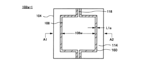
- a frame-shaped region 160 having a width L1a appears on the outer periphery of the patch electrode 108, as shown in the reflective element 102 indicated by the voltage V1 in FIG.
- Frame-shaped region 160 surrounds patch electrode 108 when viewed from above. Further, the frame-shaped region 160 may have the same width and appear along the first wiring 118 connected to the patch electrode 108.
- the width L1a is a width that becomes a standard for determining the quality of the corresponding frame-shaped area 160 when the voltage V1 is normally applied between the patch electrode 108 and the common electrode 110.
- a voltage V2 is applied between the patch electrode 108 and the common electrode 110.
- a frame-shaped region 160 having a width L2a appears on the outer periphery of the patch electrode 108, as shown in the reflective element 102 indicated by the voltage V2 in FIG. Further, the frame-shaped region 160 may appear along the first wiring 118 that has the same width and connects to the patch electrode 108.
- the width L2a is a width that serves as a standard for determining the quality of the corresponding frame-shaped region 160 when the voltage V2 is normally applied between the patch electrode 108 and the common electrode 110.
- the reference width L2a is larger than the reference width L1a, similar to the relationship in which the absolute value of the voltage V2 is larger than the absolute value of the voltage V1. Also, since the absolute value of voltage V2 is larger than the absolute value of voltage V1, the reflective element 102 has a voltage V1 that is smaller than the amount of phase change set to the reflective element 102 applied between the patch electrode 108 and the common electrode 110. A high amount of phase change can be set.
- a voltage V3 is applied between the patch electrode 108 and the common electrode 110.
- a frame-shaped region 160 having a width L3a appears on the outer periphery of the patch electrode 108, as shown in the reflective element 102 indicated by the voltage V3 in FIG. Further, the frame-shaped region 160 may appear along the first wiring 118 that has the same width and connects to the patch electrode 108.
- the width L3a is a width that serves as a reference for determining the quality of the frame-shaped region 160 when the voltage V3 is normally applied between the patch electrode 108 and the common electrode 110.
- the reference width L3a is larger than the reference width L2a, similar to the relationship where the absolute value of the voltage V3 is larger than the absolute value of the voltage V2.
- the reflective element 102 since the absolute value of voltage V3 is larger than the absolute value of voltage V2, the reflective element 102 has a voltage V2 that is smaller than the amount of phase change set to the reflective element 102 applied between the patch electrode 108 and the common electrode 110. A high amount of phase change can be set.
- a voltage V4 is applied between the patch electrode 108 and the common electrode 110.
- a frame-shaped region 160 appears on the outer periphery of the patch electrode 108, as in the reflective element 102 shown at voltage V4 in FIG. Further, the frame-shaped region 160 may appear along the first wiring 118 that has the same width and connects to the patch electrode 108.
- the width of the frame-shaped area 160 that appeared was measured, the width of the frame-shaped area 160 was width L4a.
- the width L4a is a width that serves as a standard for determining the quality of the frame-shaped region 160 when the voltage V4 is normally applied between the patch electrode 108 and the common electrode 110.
- the reference width L4a is larger than the reference width L3a, similar to the relationship where the absolute value of the voltage V4 is larger than the absolute value of the voltage V3.
- the reflective element 102 since the absolute value of voltage V4 is larger than the absolute value of voltage V3, the reflective element 102 has a voltage V3 that is smaller than the amount of phase change set in the reflective element 102 applied between the patch electrode 108 and the common electrode 110. A high amount of phase change can be set.
- the reference widths L1a to L4a can be determined by measuring the frame-shaped region 160 at each applied voltage from the radio wave reflecting device 100 actually produced as described above. Further, the reference widths L1a to L4a can also be calculated and determined from design standards taking into account the size of the patch electrode 108 of the radio wave reflection device 100, the physical property value of the cell thickness of the liquid crystal layer, and the like. The reference widths L1a to L4a can be determined without being limited to the method described above.
- determining the quality of the reflective element 102 refers to determining whether a desired voltage is normally applied to the liquid crystal layer 114 or whether a desired voltage is not normally applied to the liquid crystal layer 114. .
- FIG. 8A shows a plan view of the reflective element 102a-1 in which a frame-shaped region 160 having a reference width L1a appears.
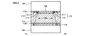
- FIG. 8B shows the reflective element 102a-2 in which a frame-shaped region 160 having a width L12 larger by ⁇ L1 than the reference width L1a appears.
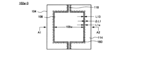
- FIG. 8C shows a reflective element 102a-3 in which a frame-shaped region L13 smaller than the reference width L1a by ⁇ L1 appears.
- the difference between the width L12 or L13 of the frame-shaped region 160 and the reference width L1a is within ⁇ L1, it can be determined that the voltage V1 is applied to the liquid crystal layer 114.
- the voltage V1 is applied between the patch electrode 108 and the common electrode 110, and the width of the frame-shaped area 160 is larger than ⁇ L1 from the reference width L1a, the reflective element It can be determined that the liquid crystal layer is not properly covered.
- 8A to 8C show examples in which the width uniformly increases or decreases with respect to the outer circumference of the patch electrode 108.
- the width L12 and the width L13 of the frame-shaped area 160 do not need to increase or decrease uniformly, and if the difference between these widths and the reference width L1a is within ⁇ L1, the voltage V1 is normally applied to the liquid crystal layer. can be determined.
- the value of ⁇ L1 can be determined by measuring the frame-shaped region 160 at each applied voltage from an actually manufactured radio wave reflecting device 100. Further, the value of the base ⁇ L1 can also be calculated and determined from a design standard taking into account the size of the patch electrode 108 of the radio wave reflecting device 100, the physical property value depending on the thickness of the cell of the liquid crystal layer, and the like.
- the method for determining ⁇ L1 is not limited to the method described above, and the same applies to ⁇ L2 to ⁇ L4, which will be described later.
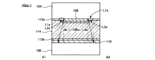
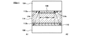
- FIG. 9A shows a cross-sectional view of reflective element 102a-1 shown in FIG. 8A.
- the frame-shaped region 160 is the upper surface of a portion of the liquid crystal layer 114.
- a part of the liquid crystal layer 114 whose top surface is the frame-shaped area 160 is formed between the patch electrode 108 and the common electrode 110 when the voltage V1 is applied between the patch electrode 108 and the common electrode 110.
- This is a liquid crystal that is oriented by an oblique electric field (up and down arrows).
- the diagonal electric fields indicated by up and down arrows are illustrative and not restrictive.
- a part of the liquid crystal layer 114 with the frame-shaped area 160 as the top surface is arranged so that the alignment of the liquid crystal is caused by leakage of an oblique electric field formed between the edge of the patch electrode 108 or its surroundings and the common electrode 110.
- diagonal electric field leakage refers to an electric field formed between the patch electrode 108 and the common electrode 110 outside the width 108w of the patch electrode 108, with respect to the electric field within the width 108w of the patch electrode 108. Point to the electric field. Therefore, as shown in FIGS.
- the orientation of the liquid crystal due to those electric fields can be visually recognized as a frame-shaped area 160 appearing on the outer periphery of the patch electrode 108 from a top view, and the alignment between the patch electrode 108 and the common electrode 110 is visible from the top. It is possible to measure the width of the frame-shaped region 160, which changes depending on the voltage applied.
- a part of the liquid crystal layer 114 that is oriented by the electric field formed outside the width 108w is connected between the patch electrode 108 and the common electrode 110 by the width 108w of the patch electrode 108. They are located so as to sandwich a liquid crystal layer 114 that is oriented by an electric field.
- the reflective element 102a-2 shown in FIG. 8B will be explained with reference to the cross-sectional view in FIG. 9B.
- a diagonal electric field (up and down arrow) is formed between the end of the patch electrode 108 and the common electrode 110. be done. Due to the formed oblique electric field, a portion of the liquid crystal layer that does not overlap with the common electrode 110 is oriented, and the oriented liquid crystal is visually recognized as a frame-shaped region 160 having a width L12 when viewed from above.
- the diagonal electric field in the reflective element 102a-1 expands more toward the common electrode 110 than in the reflective element 102a-1, but the width L12 of the frame-shaped region 160 is different from the reference width L1a. Since the difference is within ⁇ L1, it can be determined that the voltage is normally applied to the liquid crystal layer 114.
- the reflective element 102 shown in FIG. 8C will also be explained with reference to the cross-sectional view in FIG. 9C.
- a diagonal electric field (up and down arrow) is formed between the end of the patch electrode 108 and the common electrode 110. be done.
- a part of the liquid crystal layer is oriented by the formed oblique electric field, and the oriented liquid crystal is visually recognized as a frame-shaped region 160 having a width L13 when viewed from above.
- the diagonal electric field in the reflective element 102a-1 is narrower toward the common electrode 110 than that in the reflective element 102, but the width L12 of the frame-shaped region 160 is different from the reference width L1a. Since it is within ⁇ L1, it can be determined that the voltage is normally applied to the liquid crystal layer 114.
- FIGS. 10A to 10C An example of the reflective element 102 that can determine that the voltage V2 is normally applied to the liquid crystal layer 114 will be described with reference to FIGS. 10A to 10C.
- the difference from the reflective element 102 shown in FIGS. 8A to 8C and 9A to 9C is that the absolute value of the voltage applied between the patch electrode 108 and the common electrode 110 is greater than the absolute value of the voltage V1. .
- explanations may be omitted for configurations that are the same as or similar to the reflective element 102 shown in FIGS. 8A to 8C and 9A to 9C.
- FIG. 10A shows a plan view of reflective element 102a-1 to which voltage V2 is applied between patch electrode 108 and common electrode 110.
- the reference width L2a when a voltage V2 different from the voltage V1 is applied between the patch electrode 108 and the common electrode 110 is the reference width L2a when the voltage V1 is applied between the patch electrode 108 and the common electrode 110.
- the width shown is different from the reference width L1a when the width is changed. Further, since the absolute value of the voltage V2 is greater than the absolute value of the voltage V1, the reference width L2a is greater than the reference width L1a.
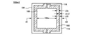
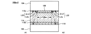
- FIGS. 10B and 10C show reflective elements 102a-2 and 102a-3, respectively, in which the width of the frame-shaped region 160 differs from the reference width L2a by ⁇ L2.
- FIG. 10B shows a reflective element 102a-2 in which a frame-shaped region 160 having a width L22 larger than the reference width L2a by ⁇ L2 appears.
- FIG. 10C shows a reflective element 102a-3 in which a frame-shaped region L23 smaller than the reference width L2a by ⁇ L2 appears. In this way, if the difference between the width L22 or L23 of the frame-shaped region 160 and the reference width L2a is within ⁇ L2, it can be determined that the voltage V2 is applied to the liquid crystal layer 114.
- the reflective element it can be determined that the liquid crystal layer is not properly covered.
- FIG. 11A shows a cross-sectional view of reflective element 102a-1 of FIG. 10A.
- the reference width L2a is larger than the reference width L1a.
- FIG. 11B shows a cross-sectional view of the reflective element 102a-2 shown in FIG. 10B.
- the diagonal electric field spreads significantly toward the common electrode 110 compared to the diagonal electric field in the reflective element 102a-1, but the width L22 of the frame-shaped region 160 is different from the reference width L2a. Since the difference is within ⁇ L2, it can be determined that the voltage is normally applied to the liquid crystal layer 114.
- FIG. 11C shows a cross-sectional view of the reflective element 102a-3 shown in FIG. 10C.
- the diagonal electric field of the reflective element 102a-3 spreads smaller toward the common electrode 110 than the diagonal electric field of the reflective element 102a-1, but the width L23 of the frame-shaped region 160 is different from the reference width L2a. Since the difference is within ⁇ L2, it can be determined that the voltage is normally applied to the liquid crystal layer 114.
- FIGS. 12A to 12C An example of the reflective element 102 that can determine that the voltage V3 is normally applied to the liquid crystal layer 114 will be described with reference to FIGS. 12A to 12C.
- the difference from the reflective element 102 shown in FIGS. 10A to 10C and FIGS. 11A to 11C is that the absolute value of the voltage applied between the patch electrode 108 and the common electrode 110 is greater than the absolute value of the voltage V2. .
- descriptions of structures that are the same as or similar to the reflective element 102 shown in FIGS. 10A to 10C and FIGS. 11A to 11C may be omitted.
- FIG. 12A shows a plan view of the reflective element 102a-1 to which the voltage V2 is applied between the patch electrode 108 and the common electrode 110.
- the reference width L3a when a voltage V3 different from the voltage V2 is applied between the patch electrode 108 and the common electrode 110 is the reference width L3a when the voltage V2 is applied between the patch electrode 108 and the common electrode 110.
- the width shown is different from the reference width L2a when the width is changed. Further, since the absolute value of voltage V3 is greater than the absolute value of voltage V2, reference width L3a is greater than reference width L2a.
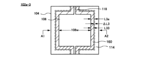
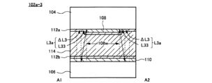
- FIGS. 12B and 12C show reflective elements 102a-2 and 102a-3, respectively, in which the width of the frame-shaped region 160 differs from the reference width L3a by ⁇ L3.
- FIG. 12B shows a reflective element 102a-2 in which a frame-shaped region 160 having a width L22 larger by ⁇ L3 than the reference width L3a appears.
- FIG. 12C shows a reflective element 102a-3 in which a frame-shaped region L23 smaller than the reference width L3a by ⁇ L3 appears. In this way, if the difference between the width L22 or L23 of the frame-shaped region 160 and the reference width L3a is within ⁇ L3, it can be determined that the voltage V3 is applied to the liquid crystal layer 114.
- the reflective element it can be determined that the liquid crystal layer is not properly covered.
- FIG. 13A shows a cross-sectional view of reflective element 102a-1 of FIG. 12A.
- the reference width L3a is larger than the reference width L2a.
- FIG. 13B shows a cross-sectional view of the reflective element 102a-2 shown in FIG. 12B.
- the oblique electric field in the reflective element 102a-1 spreads more toward the common electrode 110 than in the reflective element 102a-1, but the width L22 of the frame-shaped region 160 is Since the difference from the width L3a is within ⁇ L3, it can be determined that the voltage is normally applied to the liquid crystal layer 114.
- FIG. 13C shows a cross-sectional view of the reflective element 102a-3 shown in FIG. 12C.
- the diagonal electric field in the reflective element 102a-1 spreads smaller toward the common electrode 110 than that in the reflective element 102a-1, but the width L23 of the frame-shaped region 160 is Since the difference from the width L3a is within ⁇ L3, it can be determined that the voltage is normally applied to the liquid crystal layer 114.
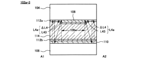
- FIGS. 14A to 14C An example of the reflective element 102 that can determine that the voltage V4 is normally applied to the liquid crystal layer 114 will be described with reference to FIGS. 14A to 14C.
- the difference from the reflective element 102 shown in FIGS. 12A to 12C and 13A to 13C is that the absolute value of the voltage V4 applied between the patch electrode 108 and the common electrode 110 is greater than the absolute value of the voltage V3. be. Note that explanations may be omitted for configurations that are the same as or similar to the reflective element 102 shown in FIGS. 12A to 12C and 13A to 13C.
- FIG. 14A shows a plan view of reflective element 102a-1 to which voltage V4 is applied between patch electrode 108 and common electrode 110.
- the reference width L4a when a voltage V4 different from the voltage V3 is applied between the patch electrode 108 and the common electrode 110 is the reference width L4a when the voltage V3 is applied between the patch electrode 108 and the common electrode 110.
- FIGS. 14B and 14C show reflective elements 102a-2 and 102a-3, respectively, in which the width of the frame-shaped region 160 differs from the reference width L4a by ⁇ L4.
- FIG. 14B shows a reflective element 102a-2 in which a frame-shaped region 160 having a width L22 larger by ⁇ L4 than the reference width L4a appears.
- FIG. 14C shows a reflective element 102a-3 in which a frame-shaped region L23 smaller than the reference width L4a by ⁇ L4 appears. In this way, if the difference between the width L22 or L23 of the frame-shaped region 160 and the reference width L4a is within ⁇ L4, it can be determined that the voltage V4 is applied to the liquid crystal layer 114.
- the reflective element it can be determined that the liquid crystal layer is not properly covered.
- FIG. 15A shows a cross-sectional view of reflective element 102a-1 of FIG. 14A.
- the reference width L4a is larger than the reference width L3a.
- FIG. 15B shows a cross-sectional view of the reflective element 102a-2 shown in FIG. 14B.
- the diagonal electric field spreads widely toward the common electrode 110 compared to the diagonal electric field in the reflective element 102a-1, but the width L22 of the frame-shaped region 160 is different from the reference width L4a. Since the difference is within ⁇ L4, it can be determined that the voltage is normally applied to the liquid crystal layer 114.
- FIG. 15C shows a cross-sectional view of the reflective element 102a-3 shown in FIG. 14C.
- the diagonal electric field spreads smaller toward the common electrode 110 than that in the reflective element 102a-1, but the width L23 of the frame-shaped region 160 differs from the reference width L4a. Since it is within ⁇ L4, it can be determined that the voltage is normally applied to the liquid crystal layer 114.
- the method for inspecting the radio wave reflecting device 100 involves applying a desired voltage between the patch electrode 108 and the common electrode 110 of each of the plurality of reflecting elements 102 of the radio wave reflecting device 100.
- the quality of each reflective element 102 can be determined based on the change in the frame-shaped area 160 appearing on the outer periphery of the patch electrode 108 when viewed from above. Such quality determination can be performed non-destructively on the radio wave reflecting device 100, and thus can be used for pre-shipment inspection of the radio wave reflecting device 100.
- the failure mode of the reflective element 102 can be determined. By determining this failure mode, failure analysis of the manufacturing process of the radio wave reflection device 100 can be performed, and the yield of the radio wave reflection device 100 can be further improved.
- FIG. 16 illustrates a top view of reflective element 102 when the desired voltage is not applied to liquid crystal layer 114.
- FIG. 16A shows an example of the reflective element 102 in failure mode A.
- the frame-shaped region 160 appears with a specified width from voltage V0 to voltage V2, and from voltage V3 to voltage V4, which are high potentials, appears with a specified width. Disappear.
- the prescribed width means, for example, a width within a difference ⁇ L1 between the voltage V1 and the reference width L1a, and a width within a difference ⁇ L2 between the voltage V2 and the reference width L2a.
- failure mode A it is assumed that there is a failure in the electrical characteristics of the switching element 134 connected to the patch electrode 108.
- FIG. 16 shows an example of the reflective element 102 in failure mode B.
- the prescribed width indicates, for example, a width within a difference ⁇ L3 between the voltage V3 and the reference width L3a, and a width within a difference ⁇ L4 between the voltage V4 and the reference width L4a. From this, it can be seen that in failure mode B, the voltage applied to the liquid crystal layer is insufficient.
- the cause of the voltage shortage is assumed to be a defect in the electrical characteristics of the switching element connected to the patch electrode 108. Furthermore, although not shown, when a frame-shaped area appears with a width other than the specified width at a high potential as described above, there is a lack of voltage applied to the liquid crystal layer, and the electrical characteristics of the switching element connected to the patch electrode 108 are affected. It is assumed that there is a defect.
- failure mode C in FIG. 16 shows an example of the reflective element 102 in failure mode C.
- voltages V0 to V4 are applied between the patch electrode 108 and the common electrode 110 in the frame-shaped region 160, no change is observed. Specifically, frame-shaped region 160 does not appear regardless of the applied voltage. From this, failure mode C is assumed to include an open failure of the switching element connected to the patch electrode 108, a connection failure between the patch electrode 108 and the switching element, and the like.
- FIG. 16D shows an example of the reflective element 102 in failure mode D.
- voltages V0 to V4 are applied between the patch electrode 108 and the common electrode 110 in the frame-shaped region 160, no change is observed. Specifically, frame-shaped region 160 appears regardless of the applied voltage. From this, in failure mode D, a short circuit between the source and drain of the switching element or a short circuit between the drain and gate is considered, and the voltage from the signal line connected to the source or the gate line connected to the gate electrode is always directly applied to the liquid crystal display. It is conceivable that a frame-shaped region will appear regardless of whether the switching element is on or off.
- 100 Radio wave reflection device, 100a: Radio wave reflection device, 100b: Radio wave reflection device, 102: Reflection element, 102a: First reflection element, 102a-1: Reflection element, 102a-2: Reflection element, 102a-3: Reflection element , 102b: second reflective element, 104: dielectric substrate (dielectric layer), 104: dielectric substrate, 106: counter substrate, 108: patch electrode, 108w: width, 110: common electrode, 110: common electrode, 112a : first alignment film, 112b: second alignment film, 114: liquid crystal layer, 116: liquid crystal molecules, 118: first wiring, 120: radio wave reflection plate, 122: peripheral area, 124: first drive circuit, 126: terminal part, 128: sealing material, 130: second drive circuit, 132: second wiring, 134: switching element, 136: undercoat layer, 138: first gate electrode, 140: first gate insulating layer, 142: semiconductor layer, 144: first connection wiring, 146: second gate insul
Landscapes
- Physics & Mathematics (AREA)
- Nonlinear Science (AREA)
- General Physics & Mathematics (AREA)
- Electromagnetism (AREA)
- Chemical & Material Sciences (AREA)
- Crystallography & Structural Chemistry (AREA)
- Optics & Photonics (AREA)
- Liquid Crystal (AREA)
Abstract
Description
図1A及び図1Bは、本発明の一実施形態に係る電波反射装置100に用いられる反射素子102を示す。図1Aは、反射素子102を上方(電波が入射する側)からみたときの平面図を示し、図1Bは平面図に示すA1-A2間の断面図を示す。
次に、反射素子が集積された電波反射装置の構成を示す。
図3は、本発明の一実施形態に係る電波反射装置100aの構成を示す。電波反射装置100は電波反射板120を有する。電波反射板120は、複数の反射素子102により構成される。複数の反射素子102は、例えば、列方向(図3に示すX軸方向)及び列方向に交差する行方向(図3に示すY軸方向)に配列される。反射素子102は、パッチ電極108が電波の入射面に向くように配置される。電波反射板120は平板状であり、この平板状の面内に複数のパッチ電極108がマトリクス状に配列される。
図3に示す電波反射装置100aは反射軸VRが一軸であるため、反射軸VRを回転軸とした方向に反射角を制御することができる。これに対し本実施形態は、二軸反射制御をすることができる電波反射装置100bの一例を示す。以下の説明においては電波反射装置100aと異なる部分を中心に説明を行う。
次に、図7、図8A~図8C、及び図9A~図9Cを参照し、電波反射装置100の検査方法を説明する。
圧V0から電圧V4は互いに異なる電圧である。さらに、それぞれの電圧V0から電圧V4の絶対値は、電圧V0から電圧V4の順に大きい。これら印加電圧は、電圧V0からV4に限らず、反射素子102が低位相差から高位相差まで設定できる範囲で適宜設定すればよい。
はじめに、図7を参照し、パッチ電極108とコモン電極110との間に印加された電圧に対応する所望の電圧が液晶層に印加された反射素子102について説明をする。
図16は、所望の電圧が液晶層114に印加されなかった場合の反射素子102の平面図を例示する。
Claims (12)
- 行方向および列方向に配列された複数の反射素子を有する電波反射装置の検査方法であって、
前記複数の反射素子は、それぞれパッチ電極と、前記パッチ電極の背面側に重なるコモン電極と、前記パッチ電極と前記コモン電極との間の液晶層と、を有し、
前記複数のパッチ電極と前記コモン電極との間に電圧V1をそれぞれ印加し、
前記複数のパッチ電極と前記コモン電極との間に電圧が印加されるときに上面視において前記複数のパッチ電極の外周に現れる枠状領域の変化に基づいて、前記反射素子の良否を判定する電波反射装置の検査方法。 - 前記枠状領域の変化は、前記複数のパッチ電極と前記コモン電極との間に電圧が印加されるときに、上面視において前記複数のパッチ電極の外周に枠状領域が現れるか否かの変化である、請求項1に記載の電波反射装置の検査方法。
- 前記電圧V1が印加されたときの前記枠状領域の幅L1と前記電圧V1に対応する枠状領域の基準幅L1aとの差がΔL1以内であるか否かを判定する、請求項1に記載の電波反射装置の検査方法。
- 前記複数のパッチ電極と前記コモン電極との間に、前記電圧V1と異なる電圧V2をそれぞれ印加し、
前記電圧V1を印加したときの前記幅L1は前記電圧V2を印加したときの前記枠状領域の幅L2と異なるか否かを判定する、請求項3に記載の電波反射装置の検査方法。 - 前記電圧V2の絶対値は、前記電圧V1の絶対値より大きく、
前記電圧V2に対応する枠状領域の基準幅L2aは、前記基準幅L1aより大きい、
請求項4に記載の電波反射装置の検査方法。 - 前記複数のパッチ電極と前記コモン電極との間に、前記電圧V1と異なる電圧V2をそれぞれ印加し、
前記電圧V2を印加したときの前記枠状領域の幅L2と前記電圧V2に対応する枠状領域の基準幅L2aとの差がΔL2以内であるか否かを判定する、請求項3に記載の電波反射装置の検査方法。 - 前記複数のパッチ電極と前記コモン電極との間に、電圧V3をそれぞれ印加し、
前記幅L2は、前記電圧V3を印加したときの前記枠状領域の幅L3と異なるか否かを判定する、請求項4に記載の電波反射装置の検査方法。 - 前記電圧V3の絶対値は、前記電圧V2の絶対値より大きく、
前記電圧V3に対応する枠状領域の基準幅L3aは、前記電圧V2に対応する枠状領域の基準幅L2aより大きい、
請求項7に記載の電波反射装置の検査方法。 - 前記複数のパッチ電極と前記コモン電極との間に、電圧V3をそれぞれ印加し、
前記電圧V3を印加したときの前記枠状領域の幅L3と前記電圧V3に対応する枠状領域の基準幅L3aとの差がΔL3以内であるか否かを判定する、請求項6に記載の電波反射装置の検査方法。 - 前記枠状領域は、上面視において前記パッチ電極を囲み、
前記枠状領域は、前記液晶層の一部の上面である、請求項1に記載の電波反射装置の検査方法。 - 前記液晶層の一部は、断面視において、前記パッチ電極と前記コモン電極との間の液晶層を挟む、請求項10に記載の電波反射装置の検査方法。
- 前記液晶層の一部は、前記パッチ電極と前記コモン電極との間に形成された斜め電界により配向する液晶層の一部である、請求項10に記載の電波反射装置の検査方法。
Priority Applications (3)
| Application Number | Priority Date | Filing Date | Title |
|---|---|---|---|
| CN202380045450.XA CN119343834A (zh) | 2022-08-01 | 2023-05-25 | 电波反射装置的检查方法 |
| JP2024538837A JPWO2024029170A1 (ja) | 2022-08-01 | 2023-05-25 | |
| US19/016,275 US20250147347A1 (en) | 2022-08-01 | 2025-01-10 | Method for inspecting reflecting device |
Applications Claiming Priority (2)
| Application Number | Priority Date | Filing Date | Title |
|---|---|---|---|
| JP2022-122666 | 2022-08-01 | ||
| JP2022122666 | 2022-08-01 |
Related Child Applications (1)
| Application Number | Title | Priority Date | Filing Date |
|---|---|---|---|
| US19/016,275 Continuation US20250147347A1 (en) | 2022-08-01 | 2025-01-10 | Method for inspecting reflecting device |
Publications (1)
| Publication Number | Publication Date |
|---|---|
| WO2024029170A1 true WO2024029170A1 (ja) | 2024-02-08 |
Family
ID=89849090
Family Applications (1)
| Application Number | Title | Priority Date | Filing Date |
|---|---|---|---|
| PCT/JP2023/019428 Ceased WO2024029170A1 (ja) | 2022-08-01 | 2023-05-25 | 電波反射装置の検査方法 |
Country Status (4)
| Country | Link |
|---|---|
| US (1) | US20250147347A1 (ja) |
| JP (1) | JPWO2024029170A1 (ja) |
| CN (1) | CN119343834A (ja) |
| WO (1) | WO2024029170A1 (ja) |
Cited By (1)
| Publication number | Priority date | Publication date | Assignee | Title |
|---|---|---|---|---|
| WO2025027981A1 (ja) * | 2023-07-31 | 2025-02-06 | 株式会社ジャパンディスプレイ | 電波反射装置の検査装置、およびその検査方法 |
Citations (6)
| Publication number | Priority date | Publication date | Assignee | Title |
|---|---|---|---|---|
| JPH055709A (ja) * | 1991-06-27 | 1993-01-14 | Matsushita Electric Ind Co Ltd | 画面検査装置 |
| JP2003194669A (ja) * | 2001-12-27 | 2003-07-09 | Seiko Epson Corp | 液晶装置の検査方法及び検査装置 |
| CN207474683U (zh) * | 2017-11-14 | 2018-06-08 | 深圳光启尖端技术有限责任公司 | 一种超材料和天线 |
| CN111077700A (zh) * | 2019-12-20 | 2020-04-28 | 江苏三月光电科技有限公司 | 一种液晶显示元件制造方法 |
| WO2020189451A1 (ja) * | 2019-03-15 | 2020-09-24 | Agc株式会社 | アンテナ装置、電子機器、窓ガラス、及び移動体 |
| JP2021517745A (ja) * | 2019-03-12 | 2021-07-26 | 信利半導体有限公司Truly Semiconductors Ltd. | 液晶アンテナ及びその製造方法 |
-
2023
- 2023-05-25 JP JP2024538837A patent/JPWO2024029170A1/ja active Pending
- 2023-05-25 WO PCT/JP2023/019428 patent/WO2024029170A1/ja not_active Ceased
- 2023-05-25 CN CN202380045450.XA patent/CN119343834A/zh active Pending
-
2025
- 2025-01-10 US US19/016,275 patent/US20250147347A1/en active Pending
Patent Citations (6)
| Publication number | Priority date | Publication date | Assignee | Title |
|---|---|---|---|---|
| JPH055709A (ja) * | 1991-06-27 | 1993-01-14 | Matsushita Electric Ind Co Ltd | 画面検査装置 |
| JP2003194669A (ja) * | 2001-12-27 | 2003-07-09 | Seiko Epson Corp | 液晶装置の検査方法及び検査装置 |
| CN207474683U (zh) * | 2017-11-14 | 2018-06-08 | 深圳光启尖端技术有限责任公司 | 一种超材料和天线 |
| JP2021517745A (ja) * | 2019-03-12 | 2021-07-26 | 信利半導体有限公司Truly Semiconductors Ltd. | 液晶アンテナ及びその製造方法 |
| WO2020189451A1 (ja) * | 2019-03-15 | 2020-09-24 | Agc株式会社 | アンテナ装置、電子機器、窓ガラス、及び移動体 |
| CN111077700A (zh) * | 2019-12-20 | 2020-04-28 | 江苏三月光电科技有限公司 | 一种液晶显示元件制造方法 |
Cited By (1)
| Publication number | Priority date | Publication date | Assignee | Title |
|---|---|---|---|---|
| WO2025027981A1 (ja) * | 2023-07-31 | 2025-02-06 | 株式会社ジャパンディスプレイ | 電波反射装置の検査装置、およびその検査方法 |
Also Published As
| Publication number | Publication date |
|---|---|
| US20250147347A1 (en) | 2025-05-08 |
| CN119343834A (zh) | 2025-01-21 |
| JPWO2024029170A1 (ja) | 2024-02-08 |
Similar Documents
| Publication | Publication Date | Title |
|---|---|---|
| US20240243484A1 (en) | Reflect array | |
| US20250149800A1 (en) | Reflecting device | |
| WO2022259891A1 (ja) | 液晶位相変調装置、移相器、フェーズドアレイアンテナ装置、及び電波反射板 | |
| US20240364008A1 (en) | Reflect array | |
| US20250015508A1 (en) | Reflect array | |
| US20250023252A1 (en) | Reflecting device having liquid crystal material | |
| US20250147347A1 (en) | Method for inspecting reflecting device | |
| CN119948701A (zh) | 显示面板一体型电波反射装置 | |
| US20250253898A1 (en) | Intelligent reflecting surface | |
| US20250093708A1 (en) | Reflecting device | |
| US20260011928A1 (en) | Intelligent reflecting surface | |
| US20250219681A1 (en) | Intelligent reflecting surface | |
| US20250379366A1 (en) | Intelligent reflecting surface and reflecting device | |
| US20250266865A1 (en) | Intelligent reflecting surface | |
| US20260003234A1 (en) | Intelligent reflecting surface | |
| US20250226588A1 (en) | Intelligent reflecting surface | |
| US20250389989A1 (en) | Intelligent reflecting surface | |
| US20250379617A1 (en) | Intelligent reflecting surface | |
| US20250149786A1 (en) | Driving method of intelligent reflecting surface | |
| WO2024185259A1 (ja) | 電波反射装置 | |
| US20250210880A1 (en) | Reflecting device | |
| WO2026088586A1 (ja) | 電波反射装置 | |
| CN121312019A (zh) | 电波反射装置的检查方法 | |
| KR20250090342A (ko) | 전파 반사 장치 | |
| KR20250091286A (ko) | 전파 반사 장치 |
Legal Events
| Date | Code | Title | Description |
|---|---|---|---|
| 121 | Ep: the epo has been informed by wipo that ep was designated in this application |
Ref document number: 23849732 Country of ref document: EP Kind code of ref document: A1 |
|
| WWE | Wipo information: entry into national phase |
Ref document number: 2024538837 Country of ref document: JP |
|
| WWE | Wipo information: entry into national phase |
Ref document number: 202380045450.X Country of ref document: CN |
|
| WWP | Wipo information: published in national office |
Ref document number: 202380045450.X Country of ref document: CN |
|
| NENP | Non-entry into the national phase |
Ref country code: DE |
|
| 122 | Ep: pct application non-entry in european phase |
Ref document number: 23849732 Country of ref document: EP Kind code of ref document: A1 |