WO2024024040A1 - パワーコンディショナ及び電力変換システム - Google Patents
パワーコンディショナ及び電力変換システム Download PDFInfo
- Publication number
- WO2024024040A1 WO2024024040A1 PCT/JP2022/029138 JP2022029138W WO2024024040A1 WO 2024024040 A1 WO2024024040 A1 WO 2024024040A1 JP 2022029138 W JP2022029138 W JP 2022029138W WO 2024024040 A1 WO2024024040 A1 WO 2024024040A1
- Authority
- WO
- WIPO (PCT)
- Prior art keywords
- limiter
- command value
- value
- power
- discharge
- Prior art date
- Legal status (The legal status is an assumption and is not a legal conclusion. Google has not performed a legal analysis and makes no representation as to the accuracy of the status listed.)
- Ceased
Links
Images



Classifications
-
- H—ELECTRICITY
- H02—GENERATION; CONVERSION OR DISTRIBUTION OF ELECTRIC POWER
- H02M—APPARATUS FOR CONVERSION BETWEEN AC AND AC, BETWEEN AC AND DC, OR BETWEEN DC AND DC, AND FOR USE WITH MAINS OR SIMILAR POWER SUPPLY SYSTEMS; CONVERSION OF DC OR AC INPUT POWER INTO SURGE OUTPUT POWER; CONTROL OR REGULATION THEREOF
- H02M7/00—Conversion of AC power input into DC power output; Conversion of DC power input into AC power output
- H02M7/42—Conversion of DC power input into AC power output without possibility of reversal
- H02M7/44—Conversion of DC power input into AC power output without possibility of reversal by static converters
- H02M7/48—Conversion of DC power input into AC power output without possibility of reversal by static converters using discharge tubes with control electrode or semiconductor devices with control electrode
-
- H—ELECTRICITY
- H02—GENERATION; CONVERSION OR DISTRIBUTION OF ELECTRIC POWER
- H02J—ELECTRIC POWER NETWORKS; CIRCUIT ARRANGEMENTS OR SYSTEMS FOR SUPPLYING OR DISTRIBUTING ELECTRIC POWER; SYSTEMS FOR STORING ELECTRIC ENERGY
- H02J3/00—Circuit arrangements for AC mains or AC distribution networks
- H02J3/28—Arrangements for balancing of the load in networks by storage of energy
- H02J3/32—Arrangements for balancing of the load in networks by storage of energy using batteries or super capacitors with converting means
-
- H—ELECTRICITY
- H02—GENERATION; CONVERSION OR DISTRIBUTION OF ELECTRIC POWER
- H02M—APPARATUS FOR CONVERSION BETWEEN AC AND AC, BETWEEN AC AND DC, OR BETWEEN DC AND DC, AND FOR USE WITH MAINS OR SIMILAR POWER SUPPLY SYSTEMS; CONVERSION OF DC OR AC INPUT POWER INTO SURGE OUTPUT POWER; CONTROL OR REGULATION THEREOF
- H02M1/00—Details of apparatus for conversion
- H02M1/0003—Details of control, feedback or regulation circuits
- H02M1/0012—Control circuits using digital or numerical techniques
-
- H—ELECTRICITY
- H02—GENERATION; CONVERSION OR DISTRIBUTION OF ELECTRIC POWER
- H02M—APPARATUS FOR CONVERSION BETWEEN AC AND AC, BETWEEN AC AND DC, OR BETWEEN DC AND DC, AND FOR USE WITH MAINS OR SIMILAR POWER SUPPLY SYSTEMS; CONVERSION OF DC OR AC INPUT POWER INTO SURGE OUTPUT POWER; CONTROL OR REGULATION THEREOF
- H02M1/00—Details of apparatus for conversion
- H02M1/0003—Details of control, feedback or regulation circuits
- H02M1/0025—Arrangements for modifying reference values, feedback values or error values in the control loop of a converter
-
- H—ELECTRICITY
- H02—GENERATION; CONVERSION OR DISTRIBUTION OF ELECTRIC POWER
- H02M—APPARATUS FOR CONVERSION BETWEEN AC AND AC, BETWEEN AC AND DC, OR BETWEEN DC AND DC, AND FOR USE WITH MAINS OR SIMILAR POWER SUPPLY SYSTEMS; CONVERSION OF DC OR AC INPUT POWER INTO SURGE OUTPUT POWER; CONTROL OR REGULATION THEREOF
- H02M7/00—Conversion of AC power input into DC power output; Conversion of DC power input into AC power output
- H02M7/42—Conversion of DC power input into AC power output without possibility of reversal
- H02M7/44—Conversion of DC power input into AC power output without possibility of reversal by static converters
- H02M7/48—Conversion of DC power input into AC power output without possibility of reversal by static converters using discharge tubes with control electrode or semiconductor devices with control electrode
- H02M7/53—Conversion of DC power input into AC power output without possibility of reversal by static converters using discharge tubes with control electrode or semiconductor devices with control electrode using devices of a triode or transistor type requiring continuous application of a control signal
- H02M7/537—Conversion of DC power input into AC power output without possibility of reversal by static converters using discharge tubes with control electrode or semiconductor devices with control electrode using devices of a triode or transistor type requiring continuous application of a control signal using semiconductor devices only, e.g. single switched pulse inverters
- H02M7/5387—Conversion of DC power input into AC power output without possibility of reversal by static converters using discharge tubes with control electrode or semiconductor devices with control electrode using devices of a triode or transistor type requiring continuous application of a control signal using semiconductor devices only, e.g. single switched pulse inverters in a bridge configuration
- H02M7/53871—Conversion of DC power input into AC power output without possibility of reversal by static converters using discharge tubes with control electrode or semiconductor devices with control electrode using devices of a triode or transistor type requiring continuous application of a control signal using semiconductor devices only, e.g. single switched pulse inverters in a bridge configuration with automatic control of output voltage or current
- H02M7/53873—Conversion of DC power input into AC power output without possibility of reversal by static converters using discharge tubes with control electrode or semiconductor devices with control electrode using devices of a triode or transistor type requiring continuous application of a control signal using semiconductor devices only, e.g. single switched pulse inverters in a bridge configuration with automatic control of output voltage or current with digital control
Definitions
- the present disclosure relates to a power conditioner and a power conversion system equipped with the same.
- a technique in which a storage battery is connected to an AC power system via a power conditioner to suppress power fluctuations in an AC power system using a storage battery.
- a gate pulse signal that drives an inverter circuit is controlled according to a command from a host device.
- a host device for example, an energy management system (EMS) disclosed in Japanese Patent Laid-Open No. 2015-149840 is known.
- the power conditioner generally does not know the operational information of the storage battery including the state of charge (SOC). Therefore, if the host device mistakenly inputs a command to the power conditioner to overcharge the battery, the power conditioner operates directly according to the charging power command value, which may lead to overcharging of the storage battery. Similarly, if the power conditioner is operated in accordance with a power command value that is commanded from a host device and is likely to cause over-discharge, there is a risk of over-discharge of the storage battery.
- SOC state of charge
- One objective of the present disclosure is to provide a power conditioner that can prevent at least one of overcharging and overdischarging of a storage battery with a simple configuration.
- a power conditioner includes an inverter circuit that connects an AC power system and a storage battery, a command value limiter, a drive signal generator, a PI controller, and a limiter regulator. Be prepared.
- the command value limiter, drive signal generator, PI controller, and limiter adjuster are configured as follows.
- the command value limiter is configured to limit the charging power command value commanded from the host device and the discharge power command value commanded from the host device.
- the drive signal generator is configured to generate a drive signal for the inverter circuit in accordance with a charging power command value limited by the command value limiter or a discharge power command value limited by the command value limiter.
- the PI controller performs a PI control for charging limitation, which is a PI control value for the deviation between the DC voltage and the charging limiter operating voltage. Configured to calculate a value.
- the PI controller sets a discharge limiting value that is a PI control value for the deviation between the DC voltage and the discharge limiter operating voltage. It is also configured to calculate a PI control value.
- the limiter adjuster is configured to strengthen the limit on the command value of charging power by the command value limiter in accordance with the PI control value for charging restriction. Further, the limiter adjuster is configured to strengthen the limit on the command value of the discharge power by the command value limiter in accordance with the PI control value for discharge restriction.
- the command value limiter multiplies the charging power command value by a charging limiting gain having a value of 0 or more and 1 or less, and multiplies the discharging power command value by a discharging limiting gain having a value of 0 or more and 1 or less.
- the limiter adjuster may be configured to reduce the charge limitation gain in accordance with the PI control value for charge limitation, and to reduce the discharge limitation gain in accordance with the PI control value for discharge limitation.
- the limiter regulator may be configured to maintain the charge limiting gain at zero while the PI control value for charge limiting is outside a predetermined range.
- the limiter adjuster may be configured to maintain the discharge limiting gain at zero while the PI control value for discharge limiting is outside a predetermined range.
- a power conditioner includes an inverter circuit that connects an AC power system and a storage battery, a command value limiter, a drive signal generator, a PI controller, and a limiter regulator. Be prepared.
- the command value limiter, drive signal generator, PI controller, and limiter adjuster are configured as follows.
- the command value limiter is configured to limit the charging power command value commanded from the host device.
- the drive signal generator is configured to generate a drive signal for the inverter circuit according to a charging power command value limited by the command value limiter.
- the PI controller performs a PI control for charging limitation, which is a PI control value for the deviation between the DC voltage and the charging limiter operating voltage. Configured to calculate a value.
- the limiter adjuster is configured to strengthen the limit on the command value of charging power by the command value limiter in accordance with the PI control value for charging restriction.
- the command value limiter may be configured to multiply the charging power command value by a charging limit gain having a value of 0 or more and 1 or less. Further, the limiter adjuster may be configured to reduce the charge limit gain according to the PI control value for charge limit. Furthermore, the limiter regulator may be configured to maintain the charge limiting gain at zero while the PI control value for charge limiting is outside a predetermined range.
- a power conditioner includes an inverter circuit that connects an AC power system and a storage battery, a command value limiter, a drive signal generator, a PI controller, and a limiter regulator. Be prepared.
- the command value limiter, drive signal generator, PI controller, and limiter adjuster are configured as follows.
- the command value limiter is configured to limit the discharge power command value commanded from the host device.
- the drive signal generator is configured to generate a drive signal for the inverter circuit according to a discharge power command value limited by a command value limiter.
- the PI controller performs PI control for discharge limitation, which is a PI control value for the deviation between the DC voltage and the discharge limiter operating voltage. Configured to calculate a value.
- the limiter adjuster is configured to strengthen the limit on the command value of the discharge power by the command value limiter in accordance with the PI control value for discharge restriction.
- the command value limiter may be configured to multiply the command value of the discharge power by a discharge limiting gain having a value of 0 or more and 1 or less. Further, the limiter adjuster may be configured to reduce the discharge limit gain according to the PI control value for discharge limit. Furthermore, the limiter adjuster may be configured to maintain the discharge limiting gain at zero while the PI control value for discharge limiting is outside a predetermined range.
- a power conversion system includes one or more power conditioners connected to a common AC power system, and a command value of charging power or discharging power for the one or more power conditioners. and a host device that commands the command value.
- the one or more power conditioners described above are power conditioners according to any one of the first to third aspects of the present disclosure.
- At least one of overcharging and overdischarging of a storage battery can be prevented with a simple configuration.
- the limit on the charging power command value by the command value limiter according to the PI control value for the deviation between the DC voltage and the charge limiter operating voltage it is possible to suppress chattering of the command value limiter caused by voltage fluctuations.
- Charging operation can be continued for as long as possible.
- chattering of the command value limiter caused by voltage fluctuations can be suppressed.
- Discharging operation can be continued as long as possible.
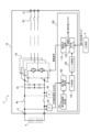
- FIG. 1 is a diagram showing a configuration of a power conditioner according to an embodiment of the present disclosure and a configuration of a power conversion system using the power conditioner.
- FIG. 3 is a diagram showing the relationship between a charge limiter operating voltage value, a discharge limiter operating voltage value, a voltage range of a power conditioner, and a voltage range of a storage battery.
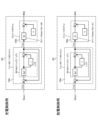
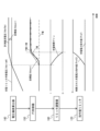
- 1 is a diagram illustrating an example of a configuration of a PI controller according to an embodiment of the present disclosure. It is a figure explaining overcharge prevention operation of a power conditioner concerning an embodiment of this indication.
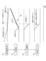
- FIG. 3 is a diagram illustrating an overdischarge prevention operation of the power conditioner according to the embodiment of the present disclosure.
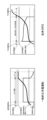
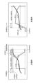
- FIG. 2 is a diagram showing an example of voltage and current movements during charging and an example of voltage and current movements during discharging by the power conditioner according to the embodiment of the present disclosure.
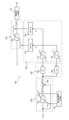
- FIG. 2 is a diagram showing a first specific example of the configuration of a control device for a power conditioner according to an embodiment of the present disclosure.
- FIG. 2 is a diagram showing a second specific example of the configuration of a control device for a power conditioner according to an embodiment of the present disclosure.
- FIG. 3 is a diagram showing a third specific example of the configuration of a control device for a power conditioner according to an embodiment of the present disclosure.
- a power conditioner is also called a power conditioning system, and is generally abbreviated as PCS.
- PCS power conditioning system
- FIG. 1 is a diagram showing the configuration of a PCS 10 and the configuration of a power conversion system 2 using the PCS 10 according to an embodiment of the present disclosure.
- the power conversion system 2 is a grid-connected distributed power supply system that combines a host device 4 and a single PCS 10 or a plurality of PCSs 10 . In the example shown in FIG. 1, only one PCS 10 is depicted for convenience.
- a storage battery 6 is connected to each PCS 10.
- the host device 4 is a controller that instructs each PCS 10 configuring the power conversion system 2 to charge or discharge.
- An example of the host device 4 is an EMS.
- the PCS 10 includes a system connection terminal 14 to which a three-phase AC power system (not shown) is connected, and a DC power supply connection terminal 12 to which the storage battery 6 is connected.
- a three-phase inverter circuit 20 is provided that converts AC power from an AC power system into DC power and reversely converts DC power from the storage battery 6 into three-phase AC power.
- the AC power system may be single-phase. In that case, a single-phase inverter circuit is provided inside the PCS 10.
- a smoothing circuit 30 is provided between the DC power supply connection terminal 12 and the inverter circuit 20 to smooth the DC current.
- the smoothing circuit is composed of a resistor and a capacitor.
- a DC current breaker 40 is provided between the DC power supply connection terminal 12 and the smoothing circuit 30 to interrupt the DC current.
- an alternating current breaker 50 is provided between the system connection terminal 14 and the inverter circuit 20 to interrupt three-phase alternating current.
- a voltmeter 80 is provided within the PCS 10.
- the voltmeter 80 measures the DC input voltage generated between the positive and negative electrodes of the DC power supply connection terminal 12.
- a voltmeter 80 may be installed between the smoothing circuit 30 and the DC current breaker 40 to measure the DC capacitor voltage of the smoothing circuit 30.
- the DC voltage measured by the voltmeter 80 is input to a control device 100, which will be described next.
- a control device 100 is provided within the PCS 10.
- the control device 100 controls the charging operation and discharging operation of the PCS 10.
- Commands from the host device 4 are input to the control device 100.
- the command input from the host device 4 to the control device 100 includes an active power command value of discharge power (hereinafter referred to as discharge power command value) for discharging power from the storage battery 6 to the AC power system, and an AC power command value.
- An active power command value of charging power (hereinafter referred to as charging power command value) for charging the storage battery 6 with power from the grid is included.
- the discharge power command value is a power command value that takes a value within the range of 0 to 100%.
- the charging power command value is a power command value that takes a value within the range of -100 to 0%.
- the controller 100 may be an application specific integrated circuit (ASIC), a field programmable gate array (FPGA), a central processing unit (CPU), or another device.
- control device 100 may be a combination of two or more ASICs, FPGAs, CPUs, or other devices.
- the ASIC, FPGA, CPU, and other devices associated with controller 100 include a series of executable instructions. When those instructions are executed, the corresponding ASIC, FPGA, CPU, and other devices are triggered to perform the functions described below.
- the instructions may be stored on a storage medium or embedded in a corresponding ASIC or FPGA.
- the control device 100 includes a drive signal generator 110, a command value limiter 120, a voltage limit range setter 130, a voltage deviation calculator 140, a PI controller 150, and a limiter adjuster 160. These are functions that are performed in a corresponding ASIC, FPGA, CPU, or another device by executing a sequence of instructions.
- the drive signal generator 110 has a gate pulse generation circuit that drives the switching elements of the inverter circuit 20.
- the drive signal generator 110 receives an input of the power command value, and generates a gate pulse signal so that the output power of the inverter circuit 20 becomes the power command value.
- the drive signal generator 110 When the input power command value is a charging power command value, the drive signal generator 110 generates a gate pulse signal that drives the inverter circuit 20 so that the storage battery 6 is charged from the AC power system.
- the drive signal generator 110 When the input power command value is a discharge power command value, the drive signal generator 110 generates a gate pulse signal that drives the inverter circuit 20 so that the storage battery 6 is discharged to the AC power system.
- the command value limiter 120 limits the power command value input from the host device 4 to the drive signal generator 110.
- the power command value input to the drive signal generator 110 is a power command value limited by the command value limiter 120. If the power command value is a charging power command value that takes a negative value, adding a limit to the power command value means correcting the power command value to a higher value command value (a command value closer to zero). It means that.
- the command value limiter 120 multiplies the charging power command value by a charging limit gain having a value of 0 or more and 1 or less.
- the limit on the charging power command value by the command value limiter 120 is automatically adjusted by a limiter adjuster 160, which will be described later.
- the power command value input to the drive signal generator 110 takes a positive value. If the power command value is a discharge power command value that takes a positive value, adding a limit to the power command value means correcting the power command value to a lower command value (a command value closer to zero). It means that.
- the command value limiter 120 multiplies the discharge power command value by a discharge limiting gain having a value of 0 or more and 1 or less. The limit on the discharge power command value by the command value limiter 120 is also automatically adjusted by a limiter adjuster 160, which will be described later.
- the voltage limit range setter 130 stores a preset charge limiter operating voltage and a preset discharge limiter operating voltage.
- the charge limiter operating voltage is a voltage that triggers the overcharge prevention operation of the PCS 10.
- the discharge limiter operating voltage is a voltage that triggers the overdischarge prevention operation of the PCS 10. The concept of setting the charge limiter operating voltage and discharge limiter operating voltage will be described later.
- the voltage deviation calculator 140 reads the charge limiter operating voltage and discharge limiter operating voltage from the voltage limit range setting device 130. Further, the voltage deviation calculator 140 acquires the DC voltage measured by the voltmeter 80 at regular intervals. The voltage deviation calculator 140 compares the measured DC voltage and the charge limiter operating voltage, and also compares the measured DC voltage and the discharge limiter operating voltage, every time the measured DC voltage is acquired from the voltmeter 80. However, the measured DC voltage used for comparison is not an instantaneous value but a moving average value over a predetermined period.
- the voltage deviation calculator 140 If the measured DC voltage is higher than the charge limiter operating voltage, the voltage deviation calculator 140 outputs the deviation of the measured DC voltage with respect to the charge limiter operating voltage. When the measured DC voltage is lower than the discharge limiter operating voltage, the voltage deviation calculator 140 outputs the deviation of the measured DC voltage with respect to the discharge limiter operating voltage. When the measured DC voltage is below the charge limiter operating voltage and above the discharge limiter operating voltage, the voltage deviation calculator 140 sets the output value to zero.
- the output of the voltage deviation calculator 140 is input to the PI controller 150.
- PI controller 150 calculates a PI control value for the output of voltage deviation calculator 140. More specifically, the PI controller 150 calculates a PI control value for the deviation between the charge limiter operating voltage and the measured DC voltage, and a PI control value for the deviation between the discharge limiter operating voltage and the measured DC voltage.
- the former is a PI control value calculated when the measured DC voltage is higher than the charging limiter operating voltage, and is used to limit charging.
- the latter is a PI control value calculated when the measured DC voltage is lower than the discharge limiter operating voltage, and is used to limit discharge.
- the calculation formula for calculating the PI control value for charge limitation and the calculation formula for calculating the PI control value for discharge limitation are defined separately.
- the PI control value for charging limitation and the PI control value for discharging limitation calculated by the PI controller 150 are each input to the limiter adjuster 160.
- the limiter adjuster 160 strengthens the restriction on the charging power command value by the command value limiter 120 in accordance with the PI control value for charging restriction.
- the PI control value for charge limitation changes in one direction, either positive or negative. Whether it changes to the positive side or the negative side depends on the setting of the proportional gain of the PI control.
- the limiter adjuster 160 increases the restriction by the command value limiter 120 linearly with respect to the change in the PI control value for charging limitation. go.
- the limiter adjuster 160 approaches the charge limit gain from 1 to zero as the PI control value for charge limit approaches the threshold value. Then, the limiter adjuster 160 sets the charge limit gain to zero when the PI control value for charge limit reaches the threshold value, and limits the charge limit while the PI control value for charge limit is outside a predetermined range defined by the threshold value. Keep the gain at zero.
- the limiter adjuster 160 strengthens the restriction on the command value of the discharge power by the command value limiter 120 according to the PI control value for discharge restriction.
- the PI control value for discharge limitation changes in one direction, either the positive side or the negative side. Whether it changes to the positive side or the negative side depends on the setting of the proportional gain of the PI control.
- the limiter adjuster 160 linearly increases the restriction by the command value limiter 120 with respect to the change in the PI control value for discharge limitation. go.
- the limiter adjuster 160 approaches the discharge limit gain from 1 to zero as the PI control value for discharge limit approaches the threshold value. Then, the limiter adjuster 160 sets the discharge limit gain to zero when the PI control value for discharge limitation reaches the threshold value, and limits the discharge while the PI control value for discharge limitation is outside a predetermined range defined by the threshold value. Keep the gain at zero.
- FIG. 2 is a diagram showing the relationship between the charge limiter operating voltage value VdclimL and the discharge limiter operating voltage value VdclimH, and the operating voltage range of the PCS 10 and the voltage range of the storage battery 6.
- the operating voltage range of the PCS 10 is generally matched to the voltage range of the storage battery 6.
- the lower limit operating voltage of the PCS 10 matches the lower limit voltage of the storage battery 6, and is set as the system lower limit voltage Vdcmin.
- the discharge limiter operating voltage value VdclimL is set to a voltage higher than the system lower limit voltage Vdcmin. For example, when the system lower limit voltage Vdcmin is 710V, the discharge limiter operating voltage value VdclimL is set to 720V.
- the upper limit operating voltage of the PCS 10 matches the upper limit voltage of the storage battery 6, and is set as the system upper limit voltage Vdcmax.
- the charging limiter operating voltage value VdclimH is set to a voltage lower than the system upper limit voltage Vdcmax. For example, when the system upper limit voltage Vdcmax is 1100V, the charging limiter operating voltage value VdclimH is set to 1090V.
- a deviation may occur between the operating voltage range of the PCS 10 and the voltage range of the storage battery 6.
- the higher one of the lower limit operating voltage of the PCS 10 and the lower limit voltage of the storage battery 6 is set as the system lower limit voltage Vdcmin.
- the lower of the upper limit operating voltage of the PCS 10 and the upper limit voltage of the storage battery 6 is set as the system upper limit voltage Vdcmax.
- the system lower limit voltage Vdcmin is set to 950V
- the system upper limit voltage Vdcmax is set to 1100V.
- the charging limiter operating voltage value VdclimL is set to a voltage higher than the system lower limit voltage Vdcmin.
- the discharge limiter operating voltage value VdclimH is set to a voltage lower than the system upper limit voltage Vdcmax.
- the upper limit operating voltage of the PCS 10 is lower than the upper limit voltage of the storage battery 6, the storage battery 6 will not be overcharged even if the upper limit operating voltage of the PCS 10 is around. Therefore, in the case of Example 2, there is no need to limit the output within the range from the discharge limiter operating voltage value VdclimH to the system upper limit voltage Vdcmax.
- FIG. 3 is a diagram showing an example of the configuration of the PI controller 150.
- the configuration of the PI controller 150 shown in the upper part of FIG. 3 is the configuration of the PI controller 150 for charge control used during charging.
- the configuration of the PI controller 150 shown in the lower part of FIG. 3 is the configuration of the PI controller 150 for controlling discharge used during discharge.
- the PI controller 150 includes a feedback control section 150a and a limiter conversion section 150b. However, feedback control section 150a having different configurations is used for charge control and discharge control. Further, limiter conversion sections 150b having different configurations are used for charging control and discharging control.
- the feedback control unit 150a for charge control includes a proportional integrator having a transfer function G02 expressed by the following equation (1).
- Kp2 is a proportional gain for charge control
- T2 is a time constant for charge control.
- the equation for determining the output Y(s) of the feedback control section 150a for charging control is expressed by the following equation (2).
- the feedback control unit 150a makes the output Y(s) follow the input X(s) using the input X(s) as a target value.
- the input X(s) in the following equation (2) is the deviation Vdcerr between the measured DC voltage Vdcfbk and the charge limiter operating voltage value VdclimH.
- the charging control limiter conversion unit 150b converts the output of the feedback control unit 150a into a PI control value G2 for charging limitation.
- a charging limiter gain K2 expressed by the following equation (3) is used for this conversion.
- the output of the feedback control section 150a is converted from a voltage to a dimensionless quantity by proportional control using the charge limiter gain K2.
- the feedback control unit 150a for discharge control includes a proportional integrator having a transfer function G01 expressed by the following equation (5).
- Kp1 is a proportional gain for discharge control
- T1 is a time constant for discharge control.
- the proportional gain Kp1 may be the same value as the proportional gain Kp2 for charging control, or may be set to a different value.
- the time constant T1 may be the same value as the time constant T2 for charging control, or may be set to a different value.
- the equation for determining the output Y(s) of the feedback control section 150a for discharge control is expressed by the following equation (6).
- the feedback control unit 150a makes the output Y(s) follow the input X(s) using the input X(s) as a target value.
- the input X(s) in the following equation (6) is the deviation Vdcerr between the measured DC voltage Vdcfbk and the discharge limiter operating voltage value VdclimL.
- the limiter conversion unit 150b for discharge control converts the output of the feedback control unit 150a into a PI control value G1 for limiting discharge.
- a discharge limiter gain K1 expressed by the following equation (7) is used for this conversion.
- the output of the feedback control section 150a is converted from a voltage to a dimensionless quantity by proportional control using the discharge limiter gain K1.
- the operation of the PCS 10 includes an overcharge prevention operation for protecting the storage battery 6 from overcharging.
- a specific example of the overcharge prevention operation of the PCS 10 is shown in FIG.
- the voltage deviation calculator 140 calculates the deviation Vdcerr between the measured DC voltage Vdcfbk and the charging limiter operating voltage value VdclimH.
- the PI controller 150 performs feedback control based on the deviation Vdcerr calculated by the voltage deviation calculator 140.
- the PI control value G2 for charging restriction converges to the value expressed by the following equation (9).
- the limiter adjuster 160 reduces the charge limit gain from 1 to zero in response to changes in the PI control value G2 for charge limit. Then, the command value limiter 120 limits the charging power command value Pref input from the host device 4 by the charging limit gain adjusted by the limiter adjuster 160, and transfers the limited charging power command value Pref2 to the drive signal generator 110. Enter. When the charging restriction gain is 1, the charging power command value Pref becomes the charging power command value Pref2 as it is, and when the charging restriction gain is zero, the charging power command value Pref2 is set to zero.
- the operation of the PCS 10 includes an overdischarge prevention operation to protect the storage battery 6 from overdischarge.
- a specific example of the overdischarge prevention operation of the PCS 10 is shown in FIG.
- the voltage deviation calculator 140 calculates the deviation Vdcerr between the measured DC voltage Vdcfbk and the discharge limiter operating voltage value VdclimL.
- the PI controller 150 performs feedback control based on the deviation Vdcerr calculated by the voltage deviation calculator 140.
- the PI control value G1 for discharge limitation converges to the value expressed by the following equation (10).
- the limiter adjuster 160 reduces the discharge limit gain from 1 to zero in accordance with a change in the PI control value G1 for discharge limit. Then, the command value limiter 120 limits the discharge power command value Pref input from the host device 4 by the discharge limit gain adjusted by the limiter adjuster 160, and transfers the limited discharge power command value Pref2 to the drive signal generator 110. Enter. When the discharge limit gain is 1, the discharge power command value Pref becomes the discharge power command value Pref2 as it is, and when the discharge limit gain is zero, the discharge power command value Pref2 is set to zero.
- the charge limit gain and the discharge limit gain are calculated based on the PI control value calculated using proportional integral control rather than simple proportional control. . If only proportional control is used instead of proportional-integral control, the DC voltage will fluctuate due to fluctuations in the voltage of the storage battery 6 and DC ripple due to switching of the inverter circuit 20, and the charging limit gain or discharge of the command value limiter 120 will change. There is a risk that the limit gain may fluctuate sharply. For example, when a 100% discharge operation is suddenly performed at the final discharge voltage, the DC voltage decreases. When the command value limiter 120 operates in response to the decrease in the DC voltage, the DC voltage increases again.
- chattering may occur in this manner.
- the charge limit gain and discharge limit gain are calculated using the PI control value obtained by proportional-integral control, chattering does not occur and smooth control is possible because the control response has a time constant.
- the PI control system for discharge limitation may be designed so that the overdischarge prevention operation of the command value limiter 120 is also faster.
- the overdischarge prevention operation of the command value limiter 120 can be made faster.
- the PI control system for charging limitation may be designed so that the overcharge prevention operation of the command value limiter 120 is also gradual. Specifically, by lengthening the time constant T2 of the I term in the calculation formula for the PI control value G2 for charge limitation, the overcharge prevention operation of the command value limiter 120 can be made gentler.
- FIG. 6 shows an example of voltage and current movements according to a general charging operation method of a storage battery. Thick lines indicate voltage, and thin lines indicate current.
- a typical charging operation method is a combination of constant voltage operation (CV operation) and constant current operation with direct current (CC operation). More specifically, CC operation is performed in the early to middle stages of discharging operation and charging operation. Then, CC operation is switched to CV operation near the full charge voltage, and the battery is fully charged without overcharging. Since CV operation continues even after full charge, in principle, current continues to flow to compensate for the battery's self-discharge.
- general charging operation methods do not have a special function to prevent over-discharging of stored electricity. In a typical charging operation method, the device is simply brought to a protective stop when the voltage drops to the protection stop voltage level of the device.
- FIG. 6 also shows an example of voltage and current behavior during charging and discharging by a conventional PCS. Thick lines indicate voltage, and thin lines indicate current.
- a conventional PCS charges or discharges a storage battery in accordance with a power command value from a host device. Therefore, in the unlikely event that the current command value is abnormal, the storage battery may become overcharged or overdischarged.
- the PCS when the voltage rises to the overcharge voltage level, the PCS is stopped to protect from overcharging, and when the voltage reaches the discharge voltage level, the PCS is stopped to protect from overdischarge. It is being said.
- the movement of voltage and current during charging by the PCS 10 according to the present embodiment is illustrated in FIG.
- the overcharge prevention operation functions so that the voltage can gradually reach the full charge voltage while monotonically decreasing the current. This can prevent the voltage from overshooting the overcharge voltage level. Furthermore, after the voltage reaches the full charge voltage, the voltage can be maintained at the full charge voltage. Furthermore, during that time, if the command value limiter 120 is not completely reduced to 0% but limited to a few percent, the current for self-discharge compensation can continue to flow through the storage battery 6.
- the overdischarge prevention operation functions to allow the voltage to gradually reach the discharge end voltage while monotonically decreasing the current. This prevents a steep voltage drop in the overdischarge region and protects the storage battery 6 from overdischarge.
- FIG. 8 is a diagram showing a first specific example of the configuration of the control device 100.
- the command value limiter 120 includes a variable limiter 122.
- the variable limiter 122 limits the positive power command value Pref, that is, the discharge power command value, to the upper limit value PreflimH.
- the upper limit value PreflimH is expressed as a percentage when the power command value Pref is set to 100%.
- the variable limiter 122 outputs the upper limit value PreflimH as the restricted power command value Pref2.
- variable limiter 122 limits the negative power command value Pref, that is, the charging power command value to the lower limit value PreflimL.
- the lower limit value PreflimL is expressed as a percentage when the power command value Pref is set to -100%.
- variable limiter 122 outputs lower limit value PreflimL as limited power command value Pref2.
- the voltage deviation calculator 140 includes a limiter 142 and a subtracter 144.
- the limiter 142 compares the charging limiter operating voltage value VdclimH set by the voltage limit range setting device 130 and the measured DC voltage Vdcfbk. If the measured DC voltage Vdcfbk is less than the charging limiter operating voltage value VdclimH, the limiter 142 outputs the measured DC voltage Vdcfbk as it is as the limited measured DC voltage Vdclim. If the measured DC voltage Vdcfbk is equal to or higher than the charging limiter operating voltage value VdclimH, the limiter 142 outputs the charging limiter operating voltage value VdclimH as the limited measured DC voltage Vdclim.
- the limiter 142 compares the discharge limiter operating voltage value VdclimL set by the voltage limit range setting device 130 with the measured DC voltage Vdcfbk. If the measured DC voltage Vdcfbk is larger than the discharge limiter operating voltage value VdclimL, the limiter 142 outputs the measured DC voltage Vdcfbk as it is as the limited measured DC voltage Vdclim. If the measured DC voltage Vdcfbk is less than or equal to the discharge limiter operating voltage value VdclimL, the limiter 142 outputs the discharge limiter operating voltage value VdclimL as the limited measured DC voltage Vdclim.
- the subtracter 144 calculates the deviation Vdcerr of the limited measured DC voltage Vdclim with respect to the measured DC voltage Vdcfbk. If the measured DC voltage Vdcfbk is greater than or equal to the charging limiter operating voltage value VdclimH, the deviation Vdcerr is the deviation between the charging limiter operating voltage value VdclimH and the measured DC voltage Vdcfbk. In this case, the deviation Vdcerr is a positive value. If the measured DC voltage Vdcfbk is less than or equal to the discharge limiter operating voltage value VdclimL, the deviation Vdcerr is the deviation between the discharge limiter operating voltage value VdclimL and the measured DC voltage Vdcfbk.
- the deviation Vdcerr in this case is a negative value.
- the measured DC voltage Vdcfbk is greater than the discharge limiter operating voltage value VdclimL and smaller than the charge limiter operating voltage value VdclimH, the deviation Vdcerr becomes zero.
- the charge limiter operating voltage value VdclimH is set to 1090V
- the discharge limiter operating voltage value VdclimL is set to 720V.
- an example of the measured DC voltage Vdcfbk during charging is 1150V
- an example of the measured DC voltage Vdcfbk during discharging is 716V.
- the limited measured DC voltage Vdclim output from the limiter 142 during charging becomes 1090V
- the deviation Vdcerr output from the subtracter 144 becomes -60V
- the limited measured DC voltage Vdclim outputted from the limiter 142 during discharge becomes 720V
- the deviation Vdcerr outputted from the subtracter 144 becomes 4V.
- the PI controller 150 of the first specific example is a PI controller 152.
- the PI controller 152 calculates a PI control value G for the deviation Vdcerr calculated by the subtracter 144.
- the PI controller 152 uses the charging control configuration and the discharging control configuration shown in FIG. 3 by switching between them. Therefore, the PI control value G output from the PI controller 152 during charging is the PI control value G2 for charging limitation.
- the PI control value G output from the PI controller 152 during discharging is the PI control value G1 for limiting discharge.
- the equation for determining the PI control value G2 for charging limitation is expressed by the following equation (11).
- the dimension of the PI control value G2 in the first specific example is a percentage. According to equation (11), if the deviation Vdcerr is -60V as in the example during charging, the PI control value G2 for charging limitation becomes -600%.
- the equation for determining the PI control value G1 for limiting discharge is expressed by the following equation (12).
- the dimension of the PI control value G1 in the first specific example is a percentage. According to equation (12), if the deviation Vdcerr is 4V as in the example during discharge, the PI control value G1 for discharge limitation is 40%.
- the limiter adjuster 160 includes a discharge limiting gain adjusting circuit including a limiter 162 and a subtracter 164, and a charging limiting gain adjusting circuit including a limiter 166 and a subtracter 168.
- the discharge limit gain adjustment circuit is a circuit that adjusts the upper limit value PreflimH of the variable limiter 122 within the range of 100% to 0%.
- the charging limit gain calculation circuit is a circuit that adjusts the lower limit value PreflimL of the variable limiter 122 within the range of -100% to 0%.
- the discharge limit gain calculation circuit and the charge limit gain calculation circuit are connected to the PI controller 152 in parallel.
- the limiter 162 constituting the discharge limit gain calculation circuit limits the PI control value G (PI control value G1 for discharge limitation) calculated by the PI controller 152 during discharge to within the range of 100% to 0%.
- the calculated PI control value GH is output. That is, if the PI control value G is 100% or less, the limiter 162 outputs the PI control value G as it is as the limited PI control value GH. If the PI control value G is higher than 100%, the limiter 162 outputs 100% as the limited PI control value GH.
- a subtracter 164 constituting a discharge limit gain calculation circuit subtracts the limited PI control value GH from a fixed value of 100%, and outputs the difference as a discharge limit gain.
- the discharge limit gain is set as the upper limit value PreflimH of the variable limiter 122.
- the limited PI control value GH remains at 40%, and the upper limit PreflimH is set to 60%.
- the power command value Pref that commands discharge is limited to 60% by the variable limiter 122, and the power command value Pref2 limited to 50% is input to the drive signal generator 110.
- the limiter 166 constituting the charge limit gain calculation circuit limits the PI control value G (PI control value G2 for charge limit) calculated by the PI controller 152 during charging to within the range of -100% to 0%, Output the limited PI control value GL. That is, if the PI control value G is -100% or more, the limiter 166 outputs the PI control value G as it is as the limited PI control value GL. If the PI control value G is lower than -100%, the limiter 166 outputs -100% as the limited PI control value GL.
- a subtracter 168 constituting a charge limit gain calculation circuit subtracts the limited PI control value GL from a fixed value of -100% and outputs the difference as a charge limit gain.
- the charging limit gain is set as the lower limit value PreflimL of the variable limiter 122.
- the limited PI control value GL is -100% and the lower limit value PreflimL is set to 0%.
- the power command value Pref that commands charging is limited to 0% by the variable limiter 122, and the power command value Pref2 limited to 0% is input to the drive signal generator 110.
- FIG. 9 is a diagram showing a second specific example of the configuration of the control device 100.
- the command value limiter 120 is composed of a variable limiter 122 as in the first specific example.
- the variable limiter 122 outputs a power command value Pref2 that is limited by an upper limit value PreflimH or a lower limit value PreflimL with respect to the power command value Pref.
- the voltage deviation calculator 140 includes a limiter 142 and a subtracter 144. If the measured DC voltage Vdcfbk is equal to or higher than the charging limiter operating voltage value VdclimH, the subtracter 144 outputs a deviation Vdcerr between the charging limiter operating voltage value VdclimH and the measured DC voltage Vdcfbk. If the measured DC voltage Vdcfbk is less than or equal to the discharge limiter operating voltage value VdclimL, the subtracter 144 outputs the deviation Vdcerr between the discharge limiter operating voltage value VdclimL and the measured DC voltage Vdcfbk.
- the PI controller 150 includes a PI controller 154 for controlling discharge and a PI controller 156 for controlling charging.
- PI controller 154 and PI controller 156 are connected to subtracter 144 in parallel.
- the PI controller 154 for discharge control has the configuration shown in the lower part of FIG. 3.
- the PI control value G1 for discharge limitation outputted from the PI controller 154 is calculated according to the above-mentioned equation (10). Assuming that the system lower limit voltage Vdcmin is 710V and the discharge limiter operating voltage value VdclimL is 720V, if the deviation Vdcerr is 4V as in the example during discharge, the PI control value G1 for discharge limitation is 0.6. Become.
- the PI controller 156 for charge control has the configuration shown in the upper part of FIG. 3.
- the PI control value G2 for charging limitation outputted from the PI controller 156 is calculated according to the above-mentioned equation (9). Assuming that the system upper limit voltage Vdcmax is 1100V and the charging limiter operating voltage value VdclimH is 1090V, if the deviation Vdcerr is -60V as in the example during charging, the PI control value G2 for charging limitation is -5. Become.
- the limiter adjuster 160 is configured with a discharge limiting gain adjusting circuit including a limiter 172 and a multiplier 174, and a charging limiting gain adjusting circuit including a limiter 176 and a multiplier 178.
- the discharge limit gain adjustment circuit is a circuit that adjusts the upper limit value PreflimH of the variable limiter 122 within the range of 100% to 0%.
- the charging limit gain adjustment circuit is a circuit that adjusts the lower limit value PreflimL of the variable limiter 122 within the range of ⁇ 100% to 0%.
- the limiter 172 constituting the discharge limiting gain adjustment circuit limits the PI control value G1 for discharging limitation calculated by the PI controller 154 within the range of 1 to 0, and outputs the limited PI control value GH.
- the PI control value G1 takes a value of 1 or less. If the PI control value G2 is greater than or equal to 0 and less than or equal to 1, the limiter 172 outputs the PI control value G1 as it is as the limited PI control value GH. If the PI control value G1 is lower than 0, the limiter 172 outputs 0 as the limited PI control value GH.
- a multiplier 174 forming a discharge limit gain calculation circuit multiplies the limited PI control value GH by a fixed value of 100%, and outputs the product as a discharge limit gain.
- the discharge limit gain is set as the upper limit value PreflimH of the variable limiter 122.
- the restricted PI control value GH is 0.6
- the upper limit PreflimH is set to 60%.
- the power command value Pref that commands discharge is limited to 60% by the variable limiter 122, and the power command value Pref2 limited to 60% is input to the drive signal generator 110.
- the limiter 176 constituting the charge limit gain calculation circuit limits the PI control value G2 for charge limit calculated by the PI controller 156 within the range of 1 to 0, and outputs the limited PI control value GL.
- the PI control value G2 takes a value of 1 or less. If the PI control value G2 is greater than or equal to 0 and less than or equal to 1, the limiter 176 outputs the PI control value G2 as it is as the limited PI control value GL. If the PI control value G2 is lower than 0, the limiter 176 outputs 0 as the limited PI control value GL.
- a multiplier 178 constituting a charge limit gain calculation circuit multiplies the limited PI control value GL by a fixed value of -100% and outputs the product as a charge limit gain.
- the charging limit gain is set as the lower limit value PreflimL of the variable limiter 122.
- the limited PI control value GL is 0, and the lower limit PreflimL is set to 0%.
- the power command value Pref that commands charging is limited to 0% by the variable limiter 122, and the power command value Pref2 limited to 0% is input to the drive signal generator 110.
- FIG. 10 is a diagram showing a third specific example of the configuration of the control device 100.
- the command value limiter 120 consists of a gain multiplier 124.
- Gain multiplier 124 multiplies power command value Pref by a gain.
- a positive power command value Pref that is, a discharge power command value, is multiplied by a discharge restriction gain within the range from 1 to 0.
- the power command value Pref having a negative value that is, the charging power command value is multiplied by a charging restriction gain within the range from 1 to 0.
- the gain multiplier 124 outputs the power command value Pref multiplied by the discharge restriction gain or the charge restriction gain as the restricted power command value Pref2.
- the voltage deviation calculator 140 includes a limiter 142 and a subtracter 144. If the measured DC voltage Vdcfbk is equal to or higher than the charging limiter operating voltage value VdclimH, the subtracter 144 outputs a deviation Vdcerr between the charging limiter operating voltage value VdclimH and the measured DC voltage Vdcfbk. If the measured DC voltage Vdcfbk is less than or equal to the discharge limiter operating voltage value VdclimL, the subtracter 144 outputs the deviation Vdcerr between the discharge limiter operating voltage value VdclimL and the measured DC voltage Vdcfbk.
- the PI controller 150 includes a PI controller 154 for controlling discharge and a PI controller 156 for limiting charging.
- the PI controller 154 for discharge control has the configuration shown in the lower part of FIG. 3, and outputs a PI control value G1 for discharge limitation.
- the PI controller 156 for charge control has the configuration shown in the upper part of FIG. 3, and outputs a PI control value G2 for charge restriction.
- the limiter adjuster 160 includes a limiter 182 for setting a discharge limit gain, a limiter 184 for setting a charge limit gain, a gain switch 186, and a switching determiner 188.
- the limiter adjuster 160 is a circuit that adjusts the discharge limit gain and the charge limit gain, which are multiplied by the power command value Pref in the gain multiplier 124, within a range of 1 to 0, respectively.
- the limiter 182 for setting the discharge limit gain limits the PI control value G1 for discharge limit calculated by the PI controller 154 within the range of 1 to 0, and outputs the limited PI control value as the discharge limit gain GH. do.
- the PI control value G1 takes a value of 1 or less. If the PI control value G1 is greater than or equal to 0 and less than or equal to 1, the limiter 182 outputs the PI control value G1 as it is as the discharge limiting gain GH. If the PI control value G1 is lower than 0, the limiter 182 outputs 0 as the limited discharge limit gain GH.
- the charge limit gain setting limiter 184 limits the charge limit PI control value G2 calculated by the PI controller 156 within the range of 1 to 0, and outputs the limited PI control value as the charge limit gain GL. do.
- the PI control value G2 takes a value of 1 or less. If the PI control value G2 is greater than or equal to 0 and less than or equal to 1, the limiter 184 outputs the PI control value G2 as it is as the charging limit gain GL. If the PI control value G2 is lower than 0, the limiter 184 outputs 0 as the limited charging limit gain GL.
- the discharge limiting gain GH output from the limiter 182 and the charging limiting gain GL output from the limiter 184 are both input to the gain switch 186.
- the gain switch 186 switches the gain to be selected between the discharge limit gain GH and the charge limit gain GL in response to a trigger signal input from the switch determiner 188.
- the gain selected by the gain switch 186 is input to the gain multiplier 124, and is multiplied by the power command value Pref as a discharge limit gain or a charge limit gain.
- the switching determiner 188 compares the power command value Pref with a reference value of zero, and inputs a trigger signal based on the comparison result to the gain switch 186.
- the switching determiner 188 inputs a trigger signal to the gain switch 186 so that the discharge limiting gain GH input from the limiter 182 is selected.
- the switching determiner 188 inputs a trigger signal to the gain switch 186 so that the charging limit gain GL input from the limiter 184 is selected. .
- the power command value Pref is a positive value, so the gain switch 186 selects the discharge limiting gain GH input from the limiter 182. As a result, the discharge limit gain GH is input to the gain multiplier 124. If the PI control value G1 calculated by the PI controller 154 is 0.6 as in the example during discharging described above, the discharge limit gain GH will be 0.6, and the gain multiplier 124 will set the power command value Pref to 0.6. Multiplyed by 5. As a result, the power command value Pref2 whose ratio to the power command value Pref is limited to 0.6 is input to the drive signal generator 110.
- the power command value Pref is a negative value, so the gain switch 186 selects the charging limit gain GL input from the limiter 184. Thereby, the charging limit gain GL is input to the gain multiplier 124. If the PI control value G2 calculated by the PI controller 156 is -5 as in the example at the time of charging described above, the charging limit gain GL becomes zero, and the power command value Pref is multiplied by zero in the gain multiplier 124. . As a result, the power command value Pref2 whose ratio to the power command value Pref is limited to zero is input to the drive signal generator 110.
- the PCS 10 according to the present embodiment can be realized by changing only the software of the control device without changing the hardware from the conventional PCS.
- the limit on the command value of charging power by the command value limiter 120 is strengthened according to the PI control value for the deviation between the measured DC voltage and the charging limiter operating voltage. Thereby, chattering of the command value limiter 120 caused by voltage fluctuations can be suppressed and charging operation can be continued as much as possible.
- the limit on the command value of the discharge power by the command value limiter 120 is strengthened according to the PI control value for the deviation between the measured DC voltage and the discharge limiter operating voltage. Thereby, chattering of the command value limiter 120 caused by voltage fluctuations can be suppressed, and the discharging operation can be continued as much as possible.
- Power conversion system 4 Host device 6 Storage battery 10 Power conditioner 20 Inverter circuit 80 Voltmeter 100 Control device 110 Drive signal generator 120 Command value limiter 130 Voltage limit range setter 140 Voltage deviation calculator 150 PI controller 160 Limiter adjuster
Landscapes
- Engineering & Computer Science (AREA)
- Power Engineering (AREA)
- Charge And Discharge Circuits For Batteries Or The Like (AREA)
- Supply And Distribution Of Alternating Current (AREA)
Abstract
Description
以下、図を参照して本開示の実施形態に係るパワーコンディショナについて説明する。パワーコンディショナは、パワーコンディショニングシステムとも呼ばれ、一般にPCSと略称される。本明細書でもパワーコンディショナをPCSと略称する。
次に、上記のごとく構成されたPCS10の動作、特に、制御装置100の動作について説明する。










次に、制御装置100の構成の具体例について図を用いて説明する。具体例間で共通の機能には共通の符号を付し、その機能についての説明を省略或いは簡略化する。
図8は制御装置100の構成の第1の具体例を示す図である。第1の具体例では、指令値リミッタ120は可変リミッタ122からなる。可変リミッタ122は正値の電力指令値Pref、すなわち、放電電力指令値を上限値PreflimHに制限する。上限値PreflimHは電力指令値Prefを100%とした場合の百分率で表わされる。電力指令値Prefが正値の場合、可変リミッタ122からは、制限された電力指令値Pref2として上限値PreflimHが出力される。


図9は制御装置100の構成の第2の具体例を示す図である。第2の具体例では、指令値リミッタ120は、第1の具体例と同様に可変リミッタ122からなる。可変リミッタ122からは、電力指令値Prefに対して上限値PreflimH或いは下限値PreflimLによって制限された電力指令値Pref2が出力される。
図10は制御装置100の構成の第3の具体例を示す図である。第3の具体例では、指令値リミッタ120はゲイン乗算器124からなる。ゲイン乗算器124は電力指令値Prefに対してゲインを乗算する。正値の電力指令値Pref、すなわち、放電電力指令値に対しては、1から0までの範囲内の放電制限ゲインが乗算される。負値の電力指令値Pref、すなわち、充電電力指令値に対しては、1から0までの範囲内の充電制限ゲインが乗算される。ゲイン乗算器124からは、制限された電力指令値Pref2として放電制限ゲイン或いは充電制限ゲインが乗算された電力指令値Prefが出力される。
以上述べたように、本実施形態に係るPCS10によれば、第1乃至第3の具体例に示されるような簡易な構成で蓄電池6の過充電と過放電を防止することができる。また、従来のPCSからハードウェアを変更することなく、制御装置のソフトウェアのみの変更によって本実施形態に係るPCS10を実現することができる。
4 上位装置
6 蓄電池
10 パワーコンディショナ
20 インバータ回路
80 電圧計
100 制御装置
110 駆動信号生成器
120 指令値リミッタ
130 電圧制限範囲設定器
140 電圧偏差算出器
150 PI制御器
160 リミッタ調整器
Claims (10)
- 交流電力系統と蓄電池とを接続するインバータ回路と、
上位装置から指令された充電電力の指令値と、前記上位装置から指令された放電電力の指令値とに対して制限を加えるように構成された指令値リミッタと、
前記指令値リミッタにより制限された前記充電電力の指令値、或いは前記指令値リミッタにより制限された前記放電電力の指令値に従って前記インバータ回路に対する駆動信号を生成するように構成された駆動信号生成器と、
前記インバータ回路に印可される直流電圧が所定の充電リミッタ作動電圧よりも高いことを受けて、前記直流電圧と前記充電リミッタ作動電圧との偏差に対するPI制御値である充電制限用のPI制御値を計算し、前記直流電圧が所定の放電リミッタ作動電圧よりも低いことを受けて、前記直流電圧と前記放電リミッタ作動電圧との偏差に対するPI制御値である放電制限用のPI制御値を計算するように構成されたPI制御器と、
前記充電制限用のPI制御値に応じて前記指令値リミッタによる前記充電電力の指令値に対する制限を強め、前記放電制限用のPI制御値に応じて前記指令値リミッタによる前記放電電力の指令値に対する制限を強めるように構成されたリミッタ調整器と、を備える
ことを特徴とするパワーコンディショナ。 - 請求項1に記載のパワーコンディショナにおいて、
前記指令値リミッタは、前記充電電力の指令値に対して0以上1以下の値を有する充電制限ゲインを掛け、前記放電電力の指令値に対して0以上1以下の値を有する放電制限ゲインを掛けるように構成され、
前記リミッタ調整器は、前記充電制限用のPI制御値に応じて前記充電制限ゲインを低下させ、前記放電制限用のPI制御値に応じて前記放電制限ゲインを低下させるように構成されている
ことを特徴とするパワーコンディショナ。 - 請求項2に記載のパワーコンディショナにおいて、
前記リミッタ調整器は、前記充電制限用のPI制御値が所定範囲から外れている間は前記充電制限ゲインをゼロに維持し、前記放電制限用のPI制御値が所定範囲から外れている間は前記放電制限ゲインをゼロに維持するように構成されている
ことを特徴とするパワーコンディショナ。 - 交流電力系統と蓄電池とを接続するインバータ回路と、
上位装置から指令された充電電力の指令値に対して制限を加えるように構成された指令値リミッタと、
前記指令値リミッタにより制限された前記充電電力の指令値に従って前記インバータ回路に対する駆動信号を生成するように構成された駆動信号生成器と、
前記インバータ回路に印可される直流電圧が所定の充電リミッタ作動電圧よりも高いことを受けて、前記直流電圧と前記充電リミッタ作動電圧との偏差に対するPI制御値を計算するように構成されたPI制御器と、
前記PI制御値に応じて前記指令値リミッタによる前記充電電力の指令値に対する制限を強めるように構成されたリミッタ調整器と、を備える
ことを特徴とするパワーコンディショナ。 - 請求項4に記載のパワーコンディショナにおいて、
前記指令値リミッタは、前記充電電力の指令値に対して0以上1以下の値を有する充電制限ゲインを掛けるように構成され、
前記リミッタ調整器は、前記PI制御値に応じて前記充電制限ゲインを低下させるように構成されている
ことを特徴とするパワーコンディショナ。 - 請求項5に記載のパワーコンディショナにおいて、
前記リミッタ調整器は、前記PI制御値が所定範囲から外れている間は前記充電制限ゲインをゼロに維持するように構成されている
ことを特徴とするパワーコンディショナ。 - 交流電力系統と蓄電池とを接続するインバータ回路と、
上位装置から指令された放電電力の指令値に対して制限を加えるように構成された指令値リミッタと、
前記指令値リミッタにより制限された前記放電電力の指令値に従って前記インバータ回路に対する駆動信号を生成するように構成された駆動信号生成器と、
前記インバータ回路に印可される直流電圧が所定の放電リミッタ作動電圧よりも低いことを受けて、前記直流電圧と前記放電リミッタ作動電圧との偏差に対するPI制御値を計算するように構成されたPI制御器と、
前記PI制御値に応じて前記指令値リミッタによる前記放電電力の指令値に対する制限を強めるように構成されたリミッタ調整器と、を備える
ことを特徴とするパワーコンディショナ。 - 請求項7に記載のパワーコンディショナにおいて、
前記指令値リミッタは、前記放電電力の指令値に対して0以上1以下の値を有する放電制限ゲインを掛けるように構成され、
前記リミッタ調整器は、前記PI制御値に応じて前記放電制限ゲインを低下させるように構成されている
ことを特徴とするパワーコンディショナ。 - 請求項8に記載のパワーコンディショナにおいて、
前記リミッタ調整器は、前記PI制御値が所定範囲から外れている間は前記放電制限ゲインをゼロに維持するように構成されている
ことを特徴とするパワーコンディショナ。 - 共通の交流電力系統に接続された1又は複数のパワーコンディショナと、
前記1又は複数のパワーコンディショナに充電電力の指令値又は放電電力の指令値を指令する上位装置と、を備え、
前記1又は複数のパワーコンディショナのそれぞれは請求項1乃至9のいずれか1項に記載のパワーコンディショナである
ことを特徴とする電力変換システム。
Priority Applications (4)
| Application Number | Priority Date | Filing Date | Title |
|---|---|---|---|
| JP2023569808A JP7666648B2 (ja) | 2022-07-28 | 2022-07-28 | パワーコンディショナ及び電力変換システム |
| CN202280052940.8A CN117813738A (zh) | 2022-07-28 | 2022-07-28 | 功率调节器及电力变换系统 |
| US18/294,560 US12500503B2 (en) | 2022-07-28 | 2022-07-28 | Power conditioner and power conversion system |
| PCT/JP2022/029138 WO2024024040A1 (ja) | 2022-07-28 | 2022-07-28 | パワーコンディショナ及び電力変換システム |
Applications Claiming Priority (1)
| Application Number | Priority Date | Filing Date | Title |
|---|---|---|---|
| PCT/JP2022/029138 WO2024024040A1 (ja) | 2022-07-28 | 2022-07-28 | パワーコンディショナ及び電力変換システム |
Publications (1)
| Publication Number | Publication Date |
|---|---|
| WO2024024040A1 true WO2024024040A1 (ja) | 2024-02-01 |
Family
ID=89705781
Family Applications (1)
| Application Number | Title | Priority Date | Filing Date |
|---|---|---|---|
| PCT/JP2022/029138 Ceased WO2024024040A1 (ja) | 2022-07-28 | 2022-07-28 | パワーコンディショナ及び電力変換システム |
Country Status (4)
| Country | Link |
|---|---|
| US (1) | US12500503B2 (ja) |
| JP (1) | JP7666648B2 (ja) |
| CN (1) | CN117813738A (ja) |
| WO (1) | WO2024024040A1 (ja) |
Citations (3)
| Publication number | Priority date | Publication date | Assignee | Title |
|---|---|---|---|---|
| JP2013021792A (ja) * | 2011-07-08 | 2013-01-31 | Sanyo Denki Co Ltd | 電力給電システム |
| JP2016140164A (ja) * | 2015-01-27 | 2016-08-04 | ニチコン株式会社 | 双方向インバータおよびそれを用いた蓄電システム |
| JP2021035313A (ja) * | 2019-08-29 | 2021-03-01 | 富士電機株式会社 | パワーコンディショナおよびパワーコンディショナシステム |
Family Cites Families (3)
| Publication number | Priority date | Publication date | Assignee | Title |
|---|---|---|---|---|
| JP6158107B2 (ja) | 2014-02-06 | 2017-07-05 | 株式会社東芝 | エネルギーマネジメントシステム |
| WO2022230142A1 (ja) * | 2021-04-28 | 2022-11-03 | 東芝三菱電機産業システム株式会社 | 交直変換装置 |
| US12416935B2 (en) * | 2022-10-05 | 2025-09-16 | Toshiba Mitsubishi-Electric Industrial Systems Corporation | Control device and power conversion system |
-
2022
- 2022-07-28 JP JP2023569808A patent/JP7666648B2/ja active Active
- 2022-07-28 WO PCT/JP2022/029138 patent/WO2024024040A1/ja not_active Ceased
- 2022-07-28 US US18/294,560 patent/US12500503B2/en active Active
- 2022-07-28 CN CN202280052940.8A patent/CN117813738A/zh active Pending
Patent Citations (3)
| Publication number | Priority date | Publication date | Assignee | Title |
|---|---|---|---|---|
| JP2013021792A (ja) * | 2011-07-08 | 2013-01-31 | Sanyo Denki Co Ltd | 電力給電システム |
| JP2016140164A (ja) * | 2015-01-27 | 2016-08-04 | ニチコン株式会社 | 双方向インバータおよびそれを用いた蓄電システム |
| JP2021035313A (ja) * | 2019-08-29 | 2021-03-01 | 富士電機株式会社 | パワーコンディショナおよびパワーコンディショナシステム |
Also Published As
| Publication number | Publication date |
|---|---|
| CN117813738A (zh) | 2024-04-02 |
| US20240339915A1 (en) | 2024-10-10 |
| US12500503B2 (en) | 2025-12-16 |
| JP7666648B2 (ja) | 2025-04-22 |
| JPWO2024024040A1 (ja) | 2024-02-01 |
Similar Documents
| Publication | Publication Date | Title |
|---|---|---|
| JP5952436B2 (ja) | バッテリエネルギー貯蔵装置の充放電制御方法及びそのためのバッテリエネルギー貯蔵装置 | |
| JP4796974B2 (ja) | 風力発電装置と蓄電装置のハイブリッドシステム,風力発電システム,電力制御装置 | |
| US10833513B2 (en) | Method, system and device for balancing individual electric energy storage cells | |
| KR101677802B1 (ko) | 에너지 저장 장치의 제어 장치 | |
| JP6455661B2 (ja) | 自立運転システム | |
| WO2019239640A1 (ja) | 蓄電池システムの制御装置および制御方法 | |
| JPWO2020084688A1 (ja) | 系統システム、制御装置及び系統システムの制御方法 | |
| JP6877640B2 (ja) | 電力変換装置および電力変換システム | |
| KR101866020B1 (ko) | 연료전지 차량의 시동 제어방법 | |
| US7649342B2 (en) | System and method of charging a battery in a power management unit | |
| CN111869036A (zh) | 一种充电控制方法及电子装置 | |
| CN113169577A (zh) | 蓄电系统以及充电控制方法 | |
| CN117962690A (zh) | 动力电池的放电允许功率控制方法、装置、车辆及介质 | |
| CN118107439B (zh) | 动力电池的回馈允许功率控制方法、装置、车辆及介质 | |
| JP7666648B2 (ja) | パワーコンディショナ及び電力変換システム | |
| US12418055B2 (en) | Power conditioning subsystem | |
| KR101977165B1 (ko) | 비상 전원용 ess 제어 시스템, 방법, 및 상기 방법을 실행시키기 위한 컴퓨터 판독 가능한 프로그램을 기록한 기록 매체 | |
| JPWO2022239057A5 (ja) | ||
| WO2022239057A1 (ja) | 蓄電システム及び系統制御システム | |
| JP7525062B2 (ja) | 蓄電池用の電力変換装置の負荷電流配分調整装置、負荷電流配分調整方法、及び負荷電流配分調整プログラム | |
| WO2020255624A1 (ja) | パワーコンディショナ | |
| JP7755148B2 (ja) | 電力貯蔵システム | |
| JP4741179B2 (ja) | 電力貯蔵機能付き無停電電源装置の制御方法とその装置 | |
| JP2014121196A (ja) | 二次電池の充電装置 | |
| JP7530302B2 (ja) | 電力システム |
Legal Events
| Date | Code | Title | Description |
|---|---|---|---|
| WWE | Wipo information: entry into national phase |
Ref document number: 2023569808 Country of ref document: JP |
|
| WWE | Wipo information: entry into national phase |
Ref document number: 202417005831 Country of ref document: IN Ref document number: 202280052940.8 Country of ref document: CN |
|
| 121 | Ep: the epo has been informed by wipo that ep was designated in this application |
Ref document number: 22953129 Country of ref document: EP Kind code of ref document: A1 |
|
| NENP | Non-entry into the national phase |
Ref country code: DE |
|
| 122 | Ep: pct application non-entry in european phase |
Ref document number: 22953129 Country of ref document: EP Kind code of ref document: A1 |
|
| WWG | Wipo information: grant in national office |
Ref document number: 18294560 Country of ref document: US |