WO2024018908A1 - ペロブスカイト膜形成方法およびペロブスカイト膜形成装置 - Google Patents
ペロブスカイト膜形成方法およびペロブスカイト膜形成装置 Download PDFInfo
- Publication number
- WO2024018908A1 WO2024018908A1 PCT/JP2023/025089 JP2023025089W WO2024018908A1 WO 2024018908 A1 WO2024018908 A1 WO 2024018908A1 JP 2023025089 W JP2023025089 W JP 2023025089W WO 2024018908 A1 WO2024018908 A1 WO 2024018908A1
- Authority
- WO
- WIPO (PCT)
- Prior art keywords
- perovskite
- film
- crystal state
- drying
- perovskite film
- Prior art date
- Legal status (The legal status is an assumption and is not a legal conclusion. Google has not performed a legal analysis and makes no representation as to the accuracy of the status listed.)
- Ceased
Links
Images

Classifications
-
- H—ELECTRICITY
- H10—SEMICONDUCTOR DEVICES; ELECTRIC SOLID-STATE DEVICES NOT OTHERWISE PROVIDED FOR
- H10K—ORGANIC ELECTRIC SOLID-STATE DEVICES
- H10K30/00—Organic devices sensitive to infrared radiation, light, electromagnetic radiation of shorter wavelength or corpuscular radiation
- H10K30/40—Organic devices sensitive to infrared radiation, light, electromagnetic radiation of shorter wavelength or corpuscular radiation comprising a p-i-n structure, e.g. having a perovskite absorber between p-type and n-type charge transport layers
-
- B—PERFORMING OPERATIONS; TRANSPORTING
- B05—SPRAYING OR ATOMISING IN GENERAL; APPLYING FLUENT MATERIALS TO SURFACES, IN GENERAL
- B05C—APPARATUS FOR APPLYING FLUENT MATERIALS TO SURFACES, IN GENERAL
- B05C11/00—Component parts, details or accessories not specifically provided for in groups B05C1/00 - B05C9/00
-
- B—PERFORMING OPERATIONS; TRANSPORTING
- B05—SPRAYING OR ATOMISING IN GENERAL; APPLYING FLUENT MATERIALS TO SURFACES, IN GENERAL
- B05C—APPARATUS FOR APPLYING FLUENT MATERIALS TO SURFACES, IN GENERAL
- B05C5/00—Apparatus in which liquid or other fluent material is projected, poured or allowed to flow on to the surface of the work
- B05C5/02—Apparatus in which liquid or other fluent material is projected, poured or allowed to flow on to the surface of the work the liquid or other fluent material being discharged through an outlet orifice by pressure, e.g. from an outlet device in contact or almost in contact, with the work
-
- B—PERFORMING OPERATIONS; TRANSPORTING
- B05—SPRAYING OR ATOMISING IN GENERAL; APPLYING FLUENT MATERIALS TO SURFACES, IN GENERAL
- B05C—APPARATUS FOR APPLYING FLUENT MATERIALS TO SURFACES, IN GENERAL
- B05C9/00—Apparatus or plant for applying liquid or other fluent material to surfaces by means not covered by any preceding group, or in which the means of applying the liquid or other fluent material is not important
- B05C9/08—Apparatus or plant for applying liquid or other fluent material to surfaces by means not covered by any preceding group, or in which the means of applying the liquid or other fluent material is not important for applying liquid or other fluent material and performing an auxiliary operation
- B05C9/12—Apparatus or plant for applying liquid or other fluent material to surfaces by means not covered by any preceding group, or in which the means of applying the liquid or other fluent material is not important for applying liquid or other fluent material and performing an auxiliary operation the auxiliary operation being performed after the application
-
- B—PERFORMING OPERATIONS; TRANSPORTING
- B05—SPRAYING OR ATOMISING IN GENERAL; APPLYING FLUENT MATERIALS TO SURFACES, IN GENERAL
- B05D—PROCESSES FOR APPLYING FLUENT MATERIALS TO SURFACES, IN GENERAL
- B05D3/00—Pretreatment of surfaces to which liquids or other fluent materials are to be applied; After-treatment of applied coatings, e.g. intermediate treating of an applied coating preparatory to subsequent applications of liquids or other fluent materials
-
- H—ELECTRICITY
- H10—SEMICONDUCTOR DEVICES; ELECTRIC SOLID-STATE DEVICES NOT OTHERWISE PROVIDED FOR
- H10K—ORGANIC ELECTRIC SOLID-STATE DEVICES
- H10K30/00—Organic devices sensitive to infrared radiation, light, electromagnetic radiation of shorter wavelength or corpuscular radiation
- H10K30/50—Photovoltaic [PV] devices
-
- H—ELECTRICITY
- H10—SEMICONDUCTOR DEVICES; ELECTRIC SOLID-STATE DEVICES NOT OTHERWISE PROVIDED FOR
- H10K—ORGANIC ELECTRIC SOLID-STATE DEVICES
- H10K71/00—Manufacture or treatment specially adapted for the organic devices covered by this subclass
- H10K71/10—Deposition of organic active material
- H10K71/12—Deposition of organic active material using liquid deposition, e.g. spin coating
-
- H—ELECTRICITY
- H10—SEMICONDUCTOR DEVICES; ELECTRIC SOLID-STATE DEVICES NOT OTHERWISE PROVIDED FOR
- H10K—ORGANIC ELECTRIC SOLID-STATE DEVICES
- H10K71/00—Manufacture or treatment specially adapted for the organic devices covered by this subclass
- H10K71/70—Testing, e.g. accelerated lifetime tests
-
- H—ELECTRICITY
- H10—SEMICONDUCTOR DEVICES; ELECTRIC SOLID-STATE DEVICES NOT OTHERWISE PROVIDED FOR
- H10K—ORGANIC ELECTRIC SOLID-STATE DEVICES
- H10K85/00—Organic materials used in the body or electrodes of devices covered by this subclass
- H10K85/50—Organic perovskites; Hybrid organic-inorganic perovskites [HOIP], e.g. CH3NH3PbI3
-
- Y—GENERAL TAGGING OF NEW TECHNOLOGICAL DEVELOPMENTS; GENERAL TAGGING OF CROSS-SECTIONAL TECHNOLOGIES SPANNING OVER SEVERAL SECTIONS OF THE IPC; TECHNICAL SUBJECTS COVERED BY FORMER USPC CROSS-REFERENCE ART COLLECTIONS [XRACs] AND DIGESTS
- Y02—TECHNOLOGIES OR APPLICATIONS FOR MITIGATION OR ADAPTATION AGAINST CLIMATE CHANGE
- Y02E—REDUCTION OF GREENHOUSE GAS [GHG] EMISSIONS, RELATED TO ENERGY GENERATION, TRANSMISSION OR DISTRIBUTION
- Y02E10/00—Energy generation through renewable energy sources
- Y02E10/50—Photovoltaic [PV] energy
- Y02E10/549—Organic PV cells
Definitions
- the present invention relates to a perovskite film forming method and a perovskite film forming apparatus for manufacturing a perovskite solar cell.
- perovskite solar cells are attracting attention as a technology that can replace conventional silicon solar cells.
- a perovskite solar cell is a solar cell that uses a perovskite semiconductor using a perovskite with a crystal structure that converts solar light energy into electricity, as disclosed in Patent Document 1, for example, and even if it is thin. It is possible to achieve conversion efficiency equivalent to that of conventional silicon-based solar cells, so it can be used in flexible formats. It also does not require rare metals and can be manufactured by coating, which requires a relatively low-temperature process. It has advantages such as being able to be formed at low cost.
- perovskite has poor stability during crystal growth, and there is a risk that the crystal state may change significantly due to slight differences in the perovskite film formation conditions such as coating and drying. Since the crystalline state of this perovskite film is directly linked to the power generation performance of the perovskite solar cell, there is a problem that unless the desired crystalline state is obtained throughout the perovskite film, the perovskite solar cell will not be able to have the desired power generation performance. Ta.
- the present invention aims to provide a perovskite film forming method and a perovskite film forming apparatus that can obtain a perovskite solar cell having stable power generation efficiency.
- the perovskite film forming method of the present invention includes a film forming step of forming a perovskite film on a substrate, a crystal state confirmation step of confirming the crystal state of the perovskite film on the substrate by measurement, and a crystal state confirmation step of confirming the crystal state of the perovskite film on the substrate by measurement. and a condition adjustment step of adjusting the implementation conditions in the film forming step for subsequent substrates based on the measurement results in the state confirmation step, and in the crystal state confirmation step, the measurement position is set to the perovskite on the substrate.
- the method is characterized in that a plurality of measurement points are provided throughout the film and numerical data is obtained at each measurement position to obtain the numerical data distribution of the crystal state in the entire perovskite film.
- the crystal state of the entire perovskite film can be understood by acquiring the numerical data distribution of the crystal state in the crystal state confirmation process, and the crystal state is improved overall in subsequent substrates.
- the condition adjustment step the conditions of the film forming step can be immediately reviewed to ensure that the conditions are correct.
- condition adjustment step the implementation conditions of the film formation step are adjusted so that the numerical data distribution obtained in the subsequent crystal state confirmation step is within a predetermined numerical range over the entire perovskite film. That's good.
- the numerical data distribution in the past crystal state confirmation step is accumulated together with information on the implementation conditions of the film forming step to form a data group, and in the condition adjustment step, information of the data group is also used. Therefore, it is preferable to adjust the implementation conditions in the film forming process for the next substrate.
- condition adjustment step can be carried out efficiently.
- the crystal state confirmation step it is preferable to obtain an absorption spectrum of the light irradiated to the perovskite film, and obtain the wavelength at the long wavelength end of the absorption spectrum as the numerical data.
- parameters directly connected to the power generation efficiency of the perovskite solar cell can be obtained at each measurement position, and the condition adjustment process can be performed based on the parameters.
- the crystal state confirmation step it is preferable to obtain an absorption spectrum of light irradiated to the perovskite film, and obtain absorbance in a short wavelength region of the absorption spectrum as the numerical data.
- the density of the crystal can be evaluated.
- the crystal state confirmation step it is preferable to obtain the surface roughness of the perovskite film as the numerical data.
- the crystal state can be understood by estimating the crystal size of the perovskite film at each measurement position, and the condition adjustment process can be performed based on this.
- the crystal state confirmation step it is preferable to obtain the peak wavelength of light emitted from the perovskite film as the numerical data by implementing a photoluminescence method.
- the film forming step includes a coating step of forming a coating film containing perovskite on the substrate by coating, and a drying step of drying the coating film formed on the substrate to form the perovskite film.
- the condition adjustment step it is preferable to adjust at least one of the conditions for forming the coating film in the coating step and the drying conditions for the coating film in the drying step.
- the crystal state confirmation step and the condition adjustment step are preferably performed each time the film forming step is performed.
- the perovskite film forming method of the present invention includes a coating step of forming a coating film containing perovskite on a substrate by coating, and drying the coating film formed on the substrate to form a perovskite film.
- a drying step for forming a film a crystal state confirmation step for confirming the crystal state of the coated film on the substrate by measurement, and a step for forming the film based on the measurement results in the crystal state confirmation step.
- a condition adjustment step of adjusting implementation conditions in the process, and in the crystal state confirmation step a plurality of measurement positions are provided over the entire coating film on the substrate, and numerical data is acquired at each measurement position.
- a perovskite film forming method for obtaining numerical data distribution of crystalline state in the entire coated film wherein the drying step includes a first drying step to increase perovskite crystal nuclei, and after the first drying step, a second drying step in which perovskite crystals are grown around the core, and the crystal state confirmation step is performed during the first drying step or after the first drying step and before the second drying step. It is characterized by being carried out.
- the crystalline state of the entire coated film can be grasped by acquiring the numerical data distribution of the crystalline state in the crystalline state confirmation process, and the overall crystalline state is improved in subsequent substrates.
- the conditions of the film forming step can be immediately reviewed to ensure that the conditions are correct.
- by performing the crystal state confirmation process before forming the perovskite film in the second drying process it is possible to separate the first drying process from the second drying process, especially in cases where the first drying process greatly affects the crystalline state of the perovskite film. drying conditions can be verified.
- the first drying step may be a reduced pressure drying step in which the coating film is held in a reduced pressure environment.
- the crystal state confirmation step is preferably carried out after a predetermined period of time has elapsed after the start of the first drying step.
- measurements at a plurality of measurement positions are preferably carried out substantially simultaneously.
- the timing of checking the crystal state at each measurement position can be made uniform, and the influence of drying conditions on the crystal state of the perovskite film can be accurately verified.
- the perovskite film forming apparatus of the present invention includes a film forming section that forms a perovskite film on a substrate, a crystal state confirmation section that confirms the crystal state of the perovskite film on the substrate by measurement,
- the crystal state checking unit provides a plurality of measurement positions throughout the perovskite film on the substrate, and obtains numerical data at each measurement position to determine the numerical data distribution of the crystal state in the entire perovskite film. It is characterized by obtaining.
- the crystal state of the entire perovskite film can be grasped by acquiring the numerical data distribution of the crystal state in the crystal state checking section, and the overall crystal state of the next substrate is improved.
- the operating conditions of the film forming section can be immediately reviewed to ensure that the conditions are correct.
- the perovskite film forming apparatus of the present invention includes a coating section that forms a coating film containing perovskite on a substrate by coating, and a coating section that dries the coating film formed on the substrate to form a perovskite film.
- a perovskite film forming apparatus that obtains a numerical data distribution of a crystalline state in the entire coating film by providing a plurality of points over the entire coating film and acquiring numerical data at each measurement position, a first drying section for increasing the number of crystal nuclei; and a second drying section for growing perovskite crystals around the crystal nuclei after the first drying step by the first drying section;
- the state confirmation unit checks the crystalline state of the coating film during the drying process by the first drying unit or after the first drying process and before the second drying process by the second drying unit. It is a feature.
- the crystal state of the entire coated film can be grasped by acquiring the numerical data distribution of the crystal state in the crystal state checking section, and the crystal state of the entire coated film is improved in subsequent substrates.
- the operating conditions of the film forming section can be immediately reviewed to ensure that the conditions are correct.
- by confirming the crystalline state before forming the perovskite film by the second drying it is possible to separate the drying process from the heating drying process, especially when the first drying process has a large effect on the crystalline state of the perovskite film. can be verified.
- the first drying section may be a reduced pressure drying section that holds the coating film in a reduced pressure environment.
- the crystal state confirmation unit has a plurality of measuring means, and each of the measuring means performs measurement at each of the measurement positions.
- the timing of checking the crystal state at each measurement position can be made uniform, and the influence of drying conditions on the crystal state of the perovskite film can be accurately verified.
- perovskite film forming method and perovskite film forming apparatus of the present invention a perovskite solar cell with stable power generation efficiency can be obtained.
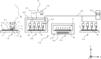
- FIG. 1 is a diagram illustrating a perovskite film forming apparatus in an embodiment of the present invention.
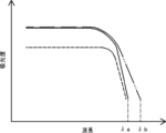
- FIG. 3 is a diagram illustrating an example of measurement results obtained in a crystal state confirmation step in the perovskite film forming method of the present embodiment.
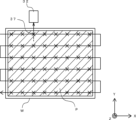
- FIG. 3 is a diagram illustrating a crystal state confirmation step in the perovskite film forming method of the present embodiment.
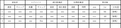
- FIG. 3 is a diagram illustrating an example of a data group accumulated in a storage device.
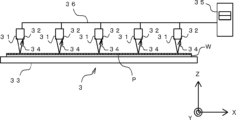
- FIG. 7 is a diagram illustrating a crystal state confirmation section in a perovskite film forming apparatus in another embodiment of the present invention.
- FIG. 7 is a diagram illustrating a perovskite film forming apparatus in another embodiment of the present invention.
- the perovskite film forming apparatus 1 has a film forming part 2 and a crystal state checking part 3, and the perovskite film forming part 2 consists of a perovskite made of a composition (perovskite) such as lead methyl ammonium iodide (MAPbI3) having a perovskite crystal structure.
- a film P is formed on a substrate W, and the crystal state of the perovskite film P formed on the substrate W is confirmed by measurement in the crystal state confirmation section 3.
- the results confirmed by the crystal state confirmation section 3 are reflected in the setting of the conditions for forming the perovskite film P on the substrate W in subsequent times by the film forming section 2, thereby forming the perovskite film P in a better crystal state.
- the substrate W is part of a perovskite solar cell, and has a hole transport layer laminated on a transparent electrode in which a transparent conductive layer is formed on a support made of a material that transmits sunlight, such as quartz glass.
- a perovskite film P is formed thereon by the perovskite film forming apparatus 1. Thereafter, an electron transport layer and a back electrode are further formed on the perovskite film P, thereby obtaining a perovskite solar cell.
- the film forming section 2 includes a coating section 10 that forms a coating film M containing perovskite on the substrate W by coating, and a drying section 20 that dries the coating film M formed on the substrate W. By drying the coating film M on the substrate W, a perovskite film P is formed.
- the application section 10 has a slit nozzle 11, a gantry 12, and a stage 13, and while the slit nozzle 11 moves relative to the substrate W held on the stage 13, the perovskite material is dissolved in the solvent.
- a coating film M is formed on the substrate W by discharging a coating liquid, which is a solution, toward the substrate W.
- the stage 13 has a substrate holding surface that is a horizontal surface on which the substrate W is placed.
- This substrate holding surface is provided with a plurality of suction holes connected to a pressure reduction means (not shown), and when the pressure reduction means operates with the substrate W placed on the substrate holding surface, the stage 13 moves the substrate. Holds W by adsorption. Note that the substrate W is placed such that the surface of the substrate W opposite to the surface on which the hole transport layer is laminated faces the substrate holding surface, and therefore the hole transport layer is laminated. The substrate W is held by suction so that the side facing upward.
- the slit nozzle 11 has a discharge port 11a located above the stage 13 and extending in the horizontal direction, and discharges the coating liquid from the discharge port 11a.
- the longitudinal direction of this discharge port 11a (the depth direction of the paper in FIG. 1) is referred to as the Y-axis direction in this explanation
- the horizontal direction perpendicular to the Y-axis direction is referred to as the X-axis direction
- the vertical direction is referred to as the Z-axis direction. call.
- a manifold 11b that is a space for storing the coating liquid and is long in the Y-axis direction like the discharge port 11a, and a slit 11c that connects the manifold 11b and the discharge port 11a.
- the manifold 11b is connected via piping to a tank (not shown) in which the coating liquid is stored, and the coating liquid sent from the tank to the manifold 11b by a pump (not shown) spreads in the Y-axis direction within the manifold 11b. It is discharged from the discharge port 11a through the slit 11c. As a result, the coating liquid is discharged in a substantially uniform discharge amount along the Y-axis direction.
- the slit nozzle 11 is attached to a gate-shaped gantry 12 that straddles the stage 13 in the Y-axis direction.
- This gantry 12 has a linear motion mechanism extending in the X-axis direction, and the slit nozzle 11 moves in the X-axis direction when this translation mechanism operates. Then, while the substrate W is held on the stage 13, the slit nozzle 11 moves above the substrate W in the X-axis direction while discharging the coating liquid from the discharge port 11a. A spreading coating film M is formed.
- the length of the discharge port 11a in the Y-axis direction is approximately equal to the length of the substrate W held on the stage 13 in the Y-axis direction, so that the slit nozzle 11 and the gantry 12 operate.
- a coating film M is formed on almost the entire surface facing the W discharge port 11a (the surface on which the hole transport layer is laminated).
- the slit nozzle 11 is attached to the gantry 12 via a linear motion mechanism (not shown) in the Z-axis direction, and the distance (gap) between the discharge port 11a and the substrate W is adjusted by the operation of this translation mechanism.
- the moving speed of the slit nozzle 11 by the gantry 12 can also be adjusted, and by controlling the gap, the moving speed of the slit nozzle 11, the feeding speed of the coating liquid from the tank to the manifold 11b, etc. Conditions for applying the coating liquid onto the substrate W are adjusted.
- the drying section 20 includes an air knife 21 that blows drying air 24 onto the coating film M immediately after coating the substrate W, a reduced pressure drying section 22 that evaporates the solvent in the coating film M by reduced pressure, and a vacuum drying section 22 that evaporates the solvent in the coating film M by reducing pressure.
- the perovskite film P is composed of three drying means including a heating drying section 23 for firing the perovskite film P to finally obtain the perovskite film P.
- the substrate W on which the coating film M has been formed by the coating section 10 is passed through an air knife 21, a vacuum drying section 22, and a heating drying section 23 in this order to dry the coating film M. In each drying means, the solvent in the coating film M is removed. As the perovskite evaporates, crystallization of the perovskite progresses in the coating film M.
- the air knife 21 is a device that blows dry air 24 downward, and is attached to the gantry 12 together with the slit nozzle 11.
- This air knife 21 is arranged so as to be close to the slit nozzle 11 on the upstream side of the slit nozzle 11 in the moving direction (X-axis direction) of the slit nozzle 11, and the slit nozzle 11, the air knife 21, and the gantry 12 operate simultaneously. Thereby, immediately after the coating liquid discharged from the slit nozzle 11 lands on the substrate W, the coating film M can be formed on the substrate W while performing initial drying with the dry air 24.
- the drying behavior of the coating film M can be controlled by the air knife 21 immediately after application.
- the gas blown from the air knife 21 is dry air 24 in this embodiment, it is not limited to this, and gases other than air such as nitrogen and argon may be used.
- the air knife 21 is attached to the gantry 12 via a Z-axis linear motion mechanism that is different from the Z-axis linear motion mechanism to which the slit nozzle 11 is attached. It can be moved separately in the Z-axis direction. Therefore, the gap between the substrate W and the air knife 21 can be adjusted separately from the gap between the substrate W and the slit nozzle 11, and the gap between the substrate W and the air knife 21, the air volume and temperature of the dry air 24 blown out from the air knife 21, etc. By controlling this, the conditions for drying the coating film M by the air knife 21 are adjusted.
- the reduced pressure drying unit 22 is a device for drying the coating film M on the substrate W under reduced pressure, and includes a reduced pressure chamber 25 in which a reduced pressure space 25a is formed, and a reduced pressure chamber 25 that is connected to the reduced pressure space 25a from the outside of the reduced pressure chamber 25 via piping 27. It has a pressure reducing means 26 such as a vacuum pump connected to.
- the reduced pressure chamber 25 has a shutter (not shown), and when the shutter is open, the substrate W is transferred from the outside of the reduced pressure chamber 25 to the reduced pressure space 25a, and when the shutter is closed, the reduced pressure space 25a is isolated from the outside air. be done.
- the decompression means 26 When the shutter of the decompression chamber 25 is in the closed state, the decompression means 26 operates to reduce the pressure in the decompression space 25a. Then, when the substrate W is placed in the reduced pressure space, the pressure in the reduced pressure space 25a is reduced, so that the boiling point of the solvent in the coating film M on the substrate W is lowered, and the solvent is volatilized. That is, the coating film M is dried under reduced pressure within the reduced pressure chamber 25.
- the drying conditions of the coating film M are adjusted by controlling the temperature of the vacuum space 25a during vacuum drying, the pressure reduction speed by the pressure reduction means 26, etc.
- the vacuum drying section 22 is also referred to as a first drying section, and the process of drying the coating film M by this vacuum drying section 22 is referred to as a first drying process.
- a phenomenon in which perovskite crystal nuclei are formed (increased) in the coating film M mainly occurs by volatilizing the solvent of the coating film M under conditions below a predetermined temperature (for example, 130°C). The longer the drying time, the more crystal nuclei are formed within the coating film M. Therefore, in this description, the first drying step is also referred to as a crystal nucleation step.
- the heating drying unit 23 is a device for baking the coating film M dried under reduced pressure by the reduced pressure drying unit 22 to obtain a perovskite film P, and includes a stage 28 on which the substrate W is placed and a heater 29 that heats the stage 28. are doing. By heating the coating film M to a temperature higher than that at which it can be fired by this heater 29, the solvent in the coating film M is further volatilized, the drying of the coating film M progresses, and the coating film M is finally fired, and the perovskite is formed. A film P is formed.
- the drying conditions of the coating film M are adjusted by adjusting the set temperature in the heating drying section 23, the heating time of the substrate W, etc.
- the heating drying section 23 is also referred to as a second drying section, and the process of drying the coating film M by this heating drying section 23 is referred to as a second drying process.
- the second drying step is also referred to as a crystal growth step.
- the perovskite film P is formed on the substrate W by the above operations of the film forming section 2 (coating section 10 and drying section 20).
- the process of forming the perovskite film P on the substrate W in this manner will be referred to as a film formation process in this description.
- the process of forming a coating film M containing perovskite on the substrate W by coating in the film forming process is called a coating process, and the coating film M formed on the substrate W is dried.
- the process of forming the perovskite film P is called a drying process.
- the crystal state confirmation unit 3 includes a light source 31, a spectrum detector 32, and a stage 33, and irradiates the perovskite film P on the substrate W held on the stage 33 with light 34 from the light source 31 to detect the perovskite film.
- a spectrum detector 32 captures the light 34 reflected by P and performs a measurement.
- the result data measured by the spectrum detector 32 is transmitted via a cable 36 to a storage device 35 .
- the stage 33 has a substrate holding surface that is a horizontal surface on which the outer peripheral portion of the substrate W is placed, and the inside of this substrate holding surface is hollow when viewed in the vertical direction.
- This substrate holding surface is provided with a plurality of suction holes connected to a pressure reducing means (not shown), and when the pressure reducing means operates with the substrate W placed on the substrate holding surface, the stage 33 moves the substrate.
- the outer periphery of W is held by suction. Note that the substrate W is placed so that the surface of the substrate W opposite to the surface on which the perovskite film P is formed faces the substrate holding surface, so that the perovskite film P faces upward.
- the substrate W is held by suction.
- the light source 31 emits light 34 including light in a predetermined wavelength range from below toward the perovskite film P, and the light 34 emitted from the light source 31 passes through the cavity of the stage 33 and reaches the bottom surface of the substrate W. reach. The light 34 then passes through the substrate W and reaches the perovskite film P.
- the light source 31 and the spectrum detector 32 are arranged such that the light 34 emitted from the light source 31 passes through the substrate W and the perovskite film P and enters the spectrum detector 32. There is.
- the light source 31 and the spectrum detector 32 are attached to a moving means (not shown) that is movable in the X-axis direction and the Y-axis direction, with the light source 31 moving below the stage 33 and the spectrum detector 32 moving above the stage 33. are moved in the X and Y directions so that they are linked to each other. Thereby, the light source 31 and the spectrum detector 32 move relative to the substrate W while maintaining the positional relationship in which the light 34 emitted from the light source 31 is incident on the spectrum detector 32.
- the storage device 35 is a memory such as a hard disk, RAM, or ROM provided in the computer, and stores the measurement result data obtained by the spectrum detector 32 transmitted from the spectrum detector 32 via the cable 36. do.
- information on the implementation conditions of the perovskite film P formation process measured by the spectrum detector 32 is also stored in advance in the storage device 35, and the upper and lower measurement result data and implementation conditions are stored in advance. A data group is formed.
- a computer equipped with this storage device 35 may be used to control the operation of each component of the film forming section 2 and the crystal state confirmation section 3.
- the photon energy hv is smaller than the band gap Eg, the light is not absorbed. Therefore, if the photon energy hv is smaller than the band gap Eg, the light is not absorbed. Therefore, if the light incident on the perovskite film P includes light in a predetermined wavelength range, and within that wavelength range there is a wavelength ⁇ that satisfies the following formula (1), then the light with a wavelength shorter than that ⁇ will become perovskite. Light that is absorbed by the film P and has a wavelength longer than ⁇ is not absorbed by the perovskite film P.
- the light 34 is emitted from the light source 31, reflected by the perovskite film P, and then made incident on the spectrum detector 32, thereby measuring the absorption spectrum.
- FIG. 2 shows an image of the measurement results of the absorption spectrum by the spectrum detector 32 at this time.
- the absorption edge in this explanation.
- the band gap Eg of the perovskite film P changes depending on the crystal state of the perovskite film P (particularly the crystal size).
- the wavelength of the absorption edge also changes from equation (1). Therefore, if the crystal state is non-uniform within the perovskite film P, even if the wavelength of the absorption edge is ⁇ a at a certain position as shown by the solid line in Figure 2, at another position it is as shown by the chain line in Figure 2.
- the wavelength of the absorption edge is a wavelength ⁇ b different from the wavelength ⁇ a.
- the band gap Eg is a value that correlates with the power generation efficiency of the solar cell, and if the band gap Eg was non-uniform within the perovskite film P, the result of measuring the band gap Eg in a part would be good. Even so, there is a possibility that good power generation efficiency cannot be obtained for the perovskite film P as a whole, which is not preferable.
- the crystal state confirmation unit 3 determines whether the wavelength of the absorption edge is substantially uniform throughout the perovskite film P. This is confirmed by measurement. Specifically, the crystal state confirmation unit 3 measures absorption spectra at multiple points on the perovskite film P while moving the light source 31 and the spectrum detector 32 in the XY directions, thereby detecting the perovskite as shown in FIG. The absorption edge wavelengths at multiple measurement positions 37 throughout the film P are measured, and the obtained multiple absorption edge wavelengths (numerical data) are summarized as the numerical data distribution of the crystal state in the perovskite film P. Obtained. Then, the numerical data distribution acquired in this way is stored in the storage device 35 together with each parameter information used in the film formation process in forming the perovskite film P.
- the process of confirming the crystal state of the perovskite film P by the above-described operation of the crystal state confirmation section 3 is referred to as a crystal state confirmation process in this description.
- the crystal state may be uneven. may occur. Therefore, in order to know whether the power generation efficiency of a perovskite solar cell using the formed perovskite film P is good or bad, it is necessary to understand the distribution of the crystal state not only in a part of the perovskite film P but also in the whole in the crystal state confirmation process as described above. is required.
- the crystal state confirmation step of this embodiment for determining the absorption edge wavelength of the absorption spectrum at each position of the perovskite film P not only allows confirmation of whether the crystal state is substantially uniform throughout the perovskite film P, but also It is also possible to calculate a parameter (band gap Eg) that is directly connected to the power generation efficiency of a perovskite solar cell.
- the density of the crystal can also be used as an evaluation index of the crystal state of the perovskite film P.
- the crystalline state of the perovskite film P be dense, and if the voids between the crystals are large and the crystalline state is sparse, the power generation efficiency will be lower than when it is dense.
- the perovskite film P is not suitable for forming a solar cell.
- the absorbance is measured to be low overall as shown by the broken line curve in FIG. be done.
- the absorbance is flat, the difference in absorbance due to the density of the crystal can be clearly seen.
- the absorbance in this short wavelength range is acquired as numerical data at each measurement position 37, and it is determined whether the absorbance in this short wavelength range is a relatively high value in the entire perovskite film P, and By evaluating whether the perovskite film P is substantially uniform, the crystal state of the perovskite film P can be confirmed.
- the absorbance in the short wavelength range may be acquired as numerical data at each measurement position 37 in addition to the wavelength of the absorption edge described above.
- the numerical data distribution obtained in the crystal state confirmation step is stored as one film formation data linked to each parameter (i.e., implementation conditions) used in the film formation step at that time. 35 and forms a data group as shown in FIG. 4 together with previously accumulated film formation data.
- the information in each row of the matrix shown in FIG. 4 is one piece of film formation data, and by accumulating a plurality of pieces of film formation data, a data group spanning multiple rows is formed. Note that in the "distribution map" portion, which is not shown in FIG. 4, a two-dimensional colored map created based on the numerical data distribution obtained in the crystal state confirmation process is stored.
- the perovskite film P is formed on the substrate W by performing the film formation process and the crystal state confirmation process using the perovskite film forming apparatus 1, and the crystal state of the perovskite film P is determined based on the numerical data distribution. After confirmation, the operator or AI feeds back information on this numerical data distribution to make adjustments to the film formation conditions used in forming this perovskite film P, and apply it to the next substrate W.
- the film formation conditions are as follows.
- each numerical data that makes up the numerical data distribution is within a predetermined numerical range, or if there is numerical data that is outside the predetermined numerical range, it is determined from which part of the perovskite film P the numerical data is located.
- condition adjustment process the process of adjusting the implementation conditions of the film forming process is referred to as a condition adjustment process, and by performing this condition adjustment process, the overall crystalline state of the perovskite film P on the substrate W is changed from next time onward. It can be improved.
- the crystal state confirmation section 3 and the crystal state confirmation process thereof be incorporated in-line. That is, each time the perovskite film P is formed in the film forming section 2, the crystal state is confirmed by the crystal state confirmation section 3, and the result is immediately fed back to the conditions for subsequent film formation in the condition adjustment step. It is preferable.
- the numerical data distribution obtained in the crystal state confirmation process is stored in the storage device 35 as film formation data together with the implementation conditions of the film formation process, and the data as shown in FIG. A group is formed. If a data group is formed in this way, the perovskite film P can be determined by changing the parameters such that the crystal state of the perovskite film P changes relatively where in the perovskite film P by changing which parameters and how. The tendency of relative change in the crystal state of the film can be understood by comparing the film formation data in the data group.
- the operator or AI who understands the trend uses the information of this data group to feed back the numerical data distribution obtained in the crystal state confirmation process in the condition adjustment process, and Adjust the conditions for carrying out the film formation process.
- the operator or AI first collects film formation data (referred to as film formation data D1) having a numerical data distribution similar to the numerical data distribution obtained in the crystal state confirmation process from the data group. Extract.
- the operator or AI extracts film formation data D2 that is similar to this film formation data D1 and has a better numerical data distribution than the film formation data D1, and combines the film formation data D1 with the film formation data D2.
- a comparison will be made of the conditions for implementing the film forming process of data D2.
- the operator or AI determines which parameters should be changed and how much should be changed for the current film forming process execution conditions, and then implements the film forming process for the next substrate W based on this. Condition. Thereby, it is possible to efficiently improve the crystal state of the perovskite film P to be formed on the next substrate W.
- this condition adjustment step is not limited to the form in which it is carried out every time the crystal state confirmation step is performed; for example, when the standard deviation of the numerical data distribution obtained in the crystal state confirmation step exceeds a predetermined threshold value. It may also be a form in which only the above is implemented. (Embodiment 2) Next, a crystal state checking section in a perovskite film forming apparatus according to another embodiment of the present invention will be described using FIG. 5.
- the crystal state confirmation unit 3 in this embodiment of the first embodiment described above as shown in FIG.
- One measuring means confirms the crystalline state of the perovskite film P at a plurality of measurement positions.
- the crystal state confirmation section 3 of this embodiment is provided with a plurality of measuring means, and each measuring means is connected to a common storage device 35. Then, the crystal state is confirmed at a plurality of measurement positions using these plurality of measurement means.
- the light 34 that has passed through the substrate W and the perovskite film P is incident on the spectrum detector 32, but in this embodiment, both the light source 31 and the spectrum detector 32 are connected to the perovskite film P.
- the light 24 reflected by the perovskite film P may be incident on the spectrum detector 32 arranged above.
- a crystal state confirmation section 3a is provided in the reduced pressure drying section 22, which is the first drying section.
- the crystal state confirmation section 3a has a plurality of measuring means as in the second embodiment, and the crystal state confirmation at a plurality of measurement positions is performed almost simultaneously using these plurality of measuring means.
- the object to be measured at this time is the coating film M containing perovskite before becoming the perovskite film P.
- the inventor has confirmed that the color tone of the coating film M varies greatly due to a slight difference in the vacuum drying time of 10 seconds in the vacuum drying process. From this, it is expected that the crystalline state (crystal nucleus density) of the perovskite in the coating film M changes significantly in a short period of time in the vacuum drying process, compared to the conditions of heat drying (second drying). It is considered that the vacuum drying conditions greatly influence the size and density of the crystals in the final perovskite film P.
- the second drying condition can be excluded and the size and density of the crystals in the perovskite film P can be adjusted. It is possible to verify the relationship between the reduced pressure drying conditions (first drying conditions) and the crystalline state of the perovskite film P, which will have a large influence.
- the crystalline state within the coating film M changes moment by moment during the reduced pressure drying process, it is possible to confirm the crystalline state at multiple measurement positions using multiple measuring means almost simultaneously as in this embodiment. It is effective to make the timing of checking the crystal state at each position uniform and to accurately verify the influence of the reduced pressure drying conditions on the crystal state of the perovskite film P.
- the crystal state confirmation section 3a is provided inside the vacuum drying section 22, but the present invention is not limited to this, and for example, the crystal state confirmation section 3a may be provided outside the vacuum drying section 22 and the first The crystal state confirmation step may be performed after the drying step and before the second drying step.
- the crystal state checking section 3a in the vacuum drying section 22 may intermittently check the crystal state of the coating film M during the vacuum drying process, and the results may be fed back in real time. It is possible to detect the timing at which the film M reaches a predetermined crystalline state (crystal nucleus density), and it is also possible to terminate the vacuum drying when the coated film M reaches a desired crystalline state.
- a crystal state checking section 3b may be provided to check the crystal state of the perovskite P after the heating drying section 23 completes the heating drying. This makes it possible to separate and verify the influence of the vacuum drying conditions and the influence of the heat drying conditions on the crystalline state of the perovskite film P.
- a plurality of heating drying units 23 are provided in parallel to ensure takt time, and it is expected that the temperature distribution in each unit will not be uniform. Therefore, the crystal state checking section 3a for checking the crystal state of the coating film M before the heat drying process and the crystal state checking section 3b for checking the crystal state of the perovskite film P after the heat drying process are provided. is preferred.
- perovskite film forming method and perovskite film forming apparatus described above it is possible to obtain a perovskite solar cell having stable power generation efficiency.
- the perovskite film forming method and perovskite film forming apparatus of the present invention are not limited to the embodiments described above, but may have other embodiments within the scope of the present invention.
- the crystal state confirmation step involves acquiring the absorption spectrum of the light irradiated to the perovskite film, and acquiring the wavelength at the long wavelength end of the absorption spectrum as the numerical data. I can't do it.
- the surface roughness of the perovskite film may be acquired as the numerical data, and it may be checked whether the numerical data is within a predetermined numerical range. By doing so, the size of the crystal of the perovskite film at each measurement position can be estimated, and the crystal state can be determined from there, so that the condition adjustment step can be performed based on this.
- a photoluminescence method in which electrons in the perovskite film P are excited by injecting a laser beam into the perovskite film P, and when the electrons return to the ground state, the emitted light from the perovskite film P is obtained. May be used. Then, it is preferable to obtain the peak wavelength of the emitted light as the numerical data and check whether the numerical data is within a predetermined numerical range. By doing so, the power generation efficiency of the perovskite film P at each measurement position can be easily grasped, as in the case of acquiring an absorption spectrum, and the condition adjustment step can be performed based on it.
- the conditions for forming the perovskite film P are adjusted so that the numerical data obtained in the subsequent crystal state confirmation steps will be approximately uniform over the entire perovskite film P.
- the conditions for forming the perovskite film P may be adjusted so that only the outer peripheral part of the perovskite film P has a different crystal state from the other parts.
- the air outlet of the air knife 21 is divided in the Y-axis direction so that the air volume and temperature of the drying air 24 can be adjusted individually, and the area where the substrate W of the stage 28 of the heating drying section 23 is placed is divided into small parts.
- the drying conditions may be made different for each small area of the perovskite film P by making it possible to individually adjust the heating temperature in each area.
- the crystal state confirmation step and the condition adjustment step are performed every time the film formation step is performed, but the crystal state confirmation step and the condition adjustment step are not limited to this, but for example, the crystal state confirmation step and the condition adjustment step are performed every multiple film formation steps. An adjustment step may also be performed.
- condition adjustment process we not only provide feedback on the implementation conditions for the next film formation process based only on the numerical data distribution for the perovskite film P that has undergone the crystal state confirmation process, but also perform film formation under the same film formation conditions. It is also possible to refer to the numerical data distribution for the perovskite film P for the most recent multiple times, and to use the tendency of change in the numerical data distribution as a criterion for feedback on the implementation conditions for the next film forming process.
- film formation data is accumulated to form a data group, but this does not necessarily have to be the case.
- the film forming section 2 is composed of the coating section 10 and the drying section 20, and the perovskite film P is formed by a coating process and a drying process, but the film forming section 2 is not limited to this, for example, by using a sputtering device. Alternatively, it may be formed by sputtering.
- the drying section 20 includes an air knife 21, a vacuum drying section 22, and a heating drying section 23, but instead of the vacuum drying section 22, a crystal nucleus formation section that performs a crystal nucleus formation process of another type (first drying section).
- a gas quench method in which air or gas is applied to the coating film M like an air knife, or a method in which a poor solvent is applied to expel the solvent in the coating film M may be used.
Landscapes
- Engineering & Computer Science (AREA)
- Chemical & Material Sciences (AREA)
- Materials Engineering (AREA)
- Manufacturing & Machinery (AREA)
- Physics & Mathematics (AREA)
- Electromagnetism (AREA)
- Crystals, And After-Treatments Of Crystals (AREA)
- Coating Apparatus (AREA)
- Photovoltaic Devices (AREA)
- Application Of Or Painting With Fluid Materials (AREA)
Abstract
Description
本発明の一実施形態におけるペロブスカイト膜形成方法を実施するためのペロブスカイト膜形成装置について、図1を参照して説明する。
上記の特性を利用するため、本実施形態では上記の通り光源31から光34を出射させ、ペロブスカイト膜Pで反射させてからスペクトル検出器32に入射させることによって、吸収スペクトルを測定している。このときのスペクトル検出器32における吸収スペクトルの測定結果のイメージを図2に示す。
(実施形態2)
次に、本発明の他の実施形態におけるペロブスカイト膜形成装置における結晶状態確認部を、図5を用いて説明する。
(実施形態3)
次に、本発明のさらに他の実施形態におけるペロブスカイト膜形成装置を、図6を用いて説明する。
2 膜形成部
3 結晶状態確認部
3a 結晶状態確認部
3b 結晶状態確認部
10 塗布部
11 スリットノズル
11a 吐出口
11b マニホールド
11c スリット
12 ガントリ
13 ステージ
20 乾燥部
21 エアナイフ
22 減圧乾燥部
23 加熱乾燥部
24 乾燥空気
25 減圧チャンバ
25a 減圧空間
26 減圧手段
27 配管
28 ステージ
29 ヒータ
31 光源
32 スペクトル検出器
33 ステージ
34 光
35 記憶装置
36 ケーブル
37 測定位置
40 上部配管
M 塗布膜
P ペロブスカイト膜
W 基板
Claims (17)
- 基板にペロブスカイト膜を形成させる膜形成工程と、
基板上の前記ペロブスカイト膜の結晶状態を測定により確認する結晶状態確認工程と、
前記結晶状態確認工程における測定結果をもとに、次回以降の基板に対する前記膜形成工程における実施条件を調節する条件調節工程と、
を有し、
前記結晶状態確認工程では、測定位置を基板上の前記ペロブスカイト膜の全体にわたって複数点設け、各測定位置で数値データを取得することによって前記ペロブスカイト膜全体における結晶状態の数値データ分布を取得することを特徴とする、ペロブスカイト膜形成方法。 - 前記条件調節工程では、次回以降の結晶状態確認工程において取得される前記数値データ分布が前記ペロブスカイト膜全体にわたって所定の数値範囲内となることを目標として、前記膜形成工程の実施条件を調節することを特徴とする、請求項1に記載のペロブスカイト膜形成方法。
- 過去の前記結晶状態確認工程における前記数値データ分布が前記膜形成工程の実施条件の情報とともに蓄積されてデータ群が形成されており、
前記条件調節工程では、前記データ群の情報も利用することにより、次回以降の基板に対する前記膜形成工程における実施条件を調節することを特徴とする、請求項1に記載のペロブスカイト膜形成方法。 - 前記結晶状態確認工程では、前記ペロブスカイト膜に照射した光の吸収スペクトルを取得し、当該吸収スペクトルの長波長側の端部の波長を前記数値データとして取得することを特徴とする、請求項1に記載のペロブスカイト膜形成方法。
- 前記結晶状態確認工程では、前記ペロブスカイト膜に照射した光の吸収スペクトルを取得し、当該吸収スペクトルの短波長域での吸光度を前記数値データとして取得することを特徴とする、請求項1に記載のペロブスカイト膜形成方法。
- 前記結晶状態確認工程では、前記ペロブスカイト膜の表面粗さを前記数値データとして取得することを特徴とする、請求項1に記載のペロブスカイト膜形成方法。
- 前記結晶状態確認工程では、フォトルミネッセンス法を実施することによって前記ペロブスカイト膜から発した光のピーク波長を前記数値データとして取得することを特徴とする、請求項1に記載のペロブスカイト膜形成方法。
- 前記膜形成工程は、塗布により基板上にペロブスカイトを含む塗布膜を形成する塗布工程と、基板上に形成された前記塗布膜を乾燥させて前記ペロブスカイト膜を形成させる乾燥工程と、を有し、
前記条件調節工程では、前記塗布工程における前記塗布膜の形成条件と前記乾燥工程における前記塗布膜の乾燥条件の少なくとも一方の調節を行うことを特徴とする、請求項1に記載のペロブスカイト膜形成方法。 - 前記結晶状態確認工程および前記条件調節工程は、前記膜形成工程を実施する毎に実施することを特徴とする、請求項1に記載のペロブスカイト膜形成方法。
- 塗布により基板上にペロブスカイトを含む塗布膜を形成する塗布工程と、基板上に形成された前記塗布膜を乾燥させてペロブスカイト膜を形成させる乾燥工程と、を含む膜形成工程と、
基板上の前記塗布膜の結晶状態を測定により確認する結晶状態確認工程と、
前記結晶状態確認工程における測定結果をもとに、前記膜形成工程における実施条件を調節する条件調節工程と、
を有し、
前記結晶状態確認工程では、測定位置を基板上の前記塗布膜の全体にわたって複数点設け、各測定位置で数値データを取得することによって前記塗布膜全体における結晶状態の数値データ分布を取得するペロブスカイト膜形成方法であって、
前記乾燥工程は、ペロブスカイトの結晶核を増やす第一の乾燥工程と、前記第一の乾燥工程後、前記結晶核を中心にペロブスカイトの結晶を成長させる第二の乾燥工程と、を有し、前記結晶状態確認工程が前記第一の乾燥工程中もしくは前記第一の乾燥工程後前記第二の乾燥工程前に行われることを特徴とする、ペロブスカイト膜形成方法。 - 前記第一の乾燥工程は、前記塗布膜を減圧環境下で保持する減圧乾燥工程であることを特徴とする、請求項10に記載のペロブスカイト膜形成方法。
- 前記結晶状態確認工程は、前記第一の乾燥工程開始後所定の時間経過後に実施されることを特徴とする、請求項10に記載のペロブスカイト膜形成方法。
- 前記結晶状態確認工程では、複数点の前記測定位置における測定を略同時に実施することを特徴とする、請求項10に記載のペロブスカイト膜形成方法。
- 基板にペロブスカイト膜を形成させる膜形成部と、
基板上の前記ペロブスカイト膜の結晶状態を測定により確認する結晶状態確認部と、
を有し、
前記結晶状態確認部では、測定位置を基板上の前記ペロブスカイト膜の全体にわたって複数点設け、各測定位置で数値データを取得することによって前記ペロブスカイト膜全体における結晶状態の数値データ分布を取得することを特徴とする、ペロブスカイト膜形成装置。 - 塗布により基板上にペロブスカイトを含む塗布膜を形成する塗布部と、基板上に形成された前記塗布膜を乾燥させてペロブスカイト膜を形成させる乾燥部と、を含む膜形成部と、
基板上の前記塗布膜の結晶状態を測定により確認する結晶状態確認部と、
を有し、
前記結晶状態確認部では、測定位置を基板上の前記塗布膜の全体にわたって複数点設け、各測定位置で数値データを取得することによって前記塗布膜全体における結晶状態の数値データ分布を取得するペロブスカイト膜形成装置であって、
前記乾燥部は、ペロブスカイトの結晶核を増やす第一の乾燥部と、前記第一の乾燥部による第一乾燥工程後、前記結晶核を中心にペロブスカイトの結晶を成長させる第二の乾燥部と、を有し、前記結晶状態確認部が前記第一の乾燥部による乾燥工程中もしくは前記第一乾燥工程後であって前記第二の乾燥部による第二の乾燥工程前に前記塗布膜の結晶状態の確認を行うことを特徴とする、ペロブスカイト膜形成装置。 - 前記第一の乾燥部は、前記塗布膜を減圧環境下で保持する減圧乾燥部であることを特徴とする、請求項15に記載のペロブスカイト膜形成装置。
- 前記結晶状態確認部は複数の測定手段を有し、それぞれの当該測定手段がそれぞれの前記測定位置における測定を実施することを特徴とする、請求項15に記載のペロブスカイト膜形成装置。
Priority Applications (2)
| Application Number | Priority Date | Filing Date | Title |
|---|---|---|---|
| US18/996,146 US20260052894A1 (en) | 2022-07-21 | 2023-07-06 | Perovskite film forming method and perovskite film forming device |
| CN202380053955.0A CN119586357A (zh) | 2022-07-21 | 2023-07-06 | 钙钛矿膜形成方法和钙钛矿膜形成装置 |
Applications Claiming Priority (2)
| Application Number | Priority Date | Filing Date | Title |
|---|---|---|---|
| JP2022116031 | 2022-07-21 | ||
| JP2022-116031 | 2022-07-21 |
Publications (1)
| Publication Number | Publication Date |
|---|---|
| WO2024018908A1 true WO2024018908A1 (ja) | 2024-01-25 |
Family
ID=89617895
Family Applications (1)
| Application Number | Title | Priority Date | Filing Date |
|---|---|---|---|
| PCT/JP2023/025089 Ceased WO2024018908A1 (ja) | 2022-07-21 | 2023-07-06 | ペロブスカイト膜形成方法およびペロブスカイト膜形成装置 |
Country Status (4)
| Country | Link |
|---|---|
| US (1) | US20260052894A1 (ja) |
| JP (1) | JP2024014771A (ja) |
| CN (1) | CN119586357A (ja) |
| WO (1) | WO2024018908A1 (ja) |
Families Citing this family (2)
| Publication number | Priority date | Publication date | Assignee | Title |
|---|---|---|---|---|
| JP2025127113A (ja) * | 2024-02-20 | 2025-09-01 | 東レエンジニアリング株式会社 | ペロブスカイト膜の評価方法、ペロブスカイト膜の形成方法及びペロブスカイト膜の形成装置 |
| JP7629568B1 (ja) | 2024-07-26 | 2025-02-13 | 株式会社ヒラノテクシード | ペロブスカイト膜形成装置及びペロブスカイト膜形成方法 |
Citations (11)
| Publication number | Priority date | Publication date | Assignee | Title |
|---|---|---|---|---|
| US20110033957A1 (en) * | 2009-08-07 | 2011-02-10 | Applied Materials, Inc. | Integrated thin film metrology system used in a solar cell production line |
| JP2016082011A (ja) * | 2014-10-15 | 2016-05-16 | 日東電工株式会社 | Cigs膜の品質評価方法およびそれを用いたcigs膜の製法、並びに当該製法によって得られたcigs膜を用いた太陽電池 |
| US20180151813A1 (en) * | 2015-05-19 | 2018-05-31 | Alliance For Sustainable Energy, Llc | Organo-metal halide perovskites films and methods of making the same |
| JP2019508902A (ja) * | 2016-03-18 | 2019-03-28 | エコール ポリテクニーク フェデラル ドゥ ローザンヌ(エーペーエフエル) | 高効率大面積ペロブスカイト太陽電池及びその製造方法 |
| CN110349886A (zh) * | 2019-06-19 | 2019-10-18 | 江苏大学 | 一种大面积钙钛矿太阳电池制备装置及制备方法 |
| JP2019212763A (ja) * | 2018-06-05 | 2019-12-12 | 住友化学株式会社 | 光電変換素子 |
| JP2020005473A (ja) * | 2018-07-02 | 2020-01-09 | パナソニックIpマネジメント株式会社 | 太陽電池の評価装置および太陽電池の評価方法 |
| CN111077165A (zh) * | 2018-10-20 | 2020-04-28 | 杭州纤纳光电科技有限公司 | 基于机器视觉的钙钛矿薄膜质量在线检测装置及方法 |
| US20200279964A1 (en) * | 2015-11-20 | 2020-09-03 | Alliance For Sustainable Energy, Llc | Multi-layered perovskites, devices, and methods of making the same |
| CN112748218A (zh) * | 2020-12-20 | 2021-05-04 | 浙江大学 | 制备钙钛矿半导体光电器件的在线实时监测系统 |
| JP2023060769A (ja) * | 2021-10-18 | 2023-04-28 | 国立大学法人電気通信大学 | ペロブスカイト層の結晶状態検査装置 |
-
2023
- 2023-07-06 JP JP2023111187A patent/JP2024014771A/ja active Pending
- 2023-07-06 CN CN202380053955.0A patent/CN119586357A/zh active Pending
- 2023-07-06 WO PCT/JP2023/025089 patent/WO2024018908A1/ja not_active Ceased
- 2023-07-06 US US18/996,146 patent/US20260052894A1/en active Pending
Patent Citations (11)
| Publication number | Priority date | Publication date | Assignee | Title |
|---|---|---|---|---|
| US20110033957A1 (en) * | 2009-08-07 | 2011-02-10 | Applied Materials, Inc. | Integrated thin film metrology system used in a solar cell production line |
| JP2016082011A (ja) * | 2014-10-15 | 2016-05-16 | 日東電工株式会社 | Cigs膜の品質評価方法およびそれを用いたcigs膜の製法、並びに当該製法によって得られたcigs膜を用いた太陽電池 |
| US20180151813A1 (en) * | 2015-05-19 | 2018-05-31 | Alliance For Sustainable Energy, Llc | Organo-metal halide perovskites films and methods of making the same |
| US20200279964A1 (en) * | 2015-11-20 | 2020-09-03 | Alliance For Sustainable Energy, Llc | Multi-layered perovskites, devices, and methods of making the same |
| JP2019508902A (ja) * | 2016-03-18 | 2019-03-28 | エコール ポリテクニーク フェデラル ドゥ ローザンヌ(エーペーエフエル) | 高効率大面積ペロブスカイト太陽電池及びその製造方法 |
| JP2019212763A (ja) * | 2018-06-05 | 2019-12-12 | 住友化学株式会社 | 光電変換素子 |
| JP2020005473A (ja) * | 2018-07-02 | 2020-01-09 | パナソニックIpマネジメント株式会社 | 太陽電池の評価装置および太陽電池の評価方法 |
| CN111077165A (zh) * | 2018-10-20 | 2020-04-28 | 杭州纤纳光电科技有限公司 | 基于机器视觉的钙钛矿薄膜质量在线检测装置及方法 |
| CN110349886A (zh) * | 2019-06-19 | 2019-10-18 | 江苏大学 | 一种大面积钙钛矿太阳电池制备装置及制备方法 |
| CN112748218A (zh) * | 2020-12-20 | 2021-05-04 | 浙江大学 | 制备钙钛矿半导体光电器件的在线实时监测系统 |
| JP2023060769A (ja) * | 2021-10-18 | 2023-04-28 | 国立大学法人電気通信大学 | ペロブスカイト層の結晶状態検査装置 |
Also Published As
| Publication number | Publication date |
|---|---|
| JP2024014771A (ja) | 2024-02-01 |
| US20260052894A1 (en) | 2026-02-19 |
| CN119586357A (zh) | 2025-03-07 |
Similar Documents
| Publication | Publication Date | Title |
|---|---|---|
| WO2024018908A1 (ja) | ペロブスカイト膜形成方法およびペロブスカイト膜形成装置 | |
| Remeika et al. | Transferrable optimization of spray-coated PbI 2 films for perovskite solar cell fabrication | |
| US20060185588A1 (en) | Vapor deposition apparatus measuring film thickness by irradiating light | |
| Hu et al. | A high-precision, template-assisted, anisotropic wet etching method for fabricating perovskite microstructure arrays | |
| US8633378B2 (en) | Method of setting conditions for film deposition, photovoltaic device, and production process, production apparatus and test method for same | |
| CN109461795A (zh) | 一种提高无机钙钛矿量子点发光效率的方法 | |
| CN205223338U (zh) | 纳秒脉冲激光退火装置 | |
| CN108257848B (zh) | 紫外光产生用靶及其制造方法以及电子束激发紫外光源 | |
| Costa et al. | In-situ and ex-situ study of proton and electron irradiations of perovskite solar cells | |
| CN105355565A (zh) | 一种电子束退火制备氧化锌薄膜的方法 | |
| Barreto et al. | Broad range adjustable emission of stacked SiNx/SiOy layers | |
| JP2011233327A (ja) | 有機el乾燥方法および装置および有機el素子 | |
| CN108140691A (zh) | 用于稳定光伏硅太阳能电池的方法和装置 | |
| CN105200376A (zh) | 用纳秒脉冲激光退火制备纳米硅发光材料的方法及装置 | |
| Escobar-Alarcón et al. | Influence of the plasma parameters on the properties of aluminum oxide thin films deposited by laser ablation | |
| JP2025127113A (ja) | ペロブスカイト膜の評価方法、ペロブスカイト膜の形成方法及びペロブスカイト膜の形成装置 | |
| KR20130125954A (ko) | 막 두께 측정 장치 | |
| CN118360579B (zh) | 基于金属靶材制作钙钛矿薄膜的方法 | |
| CN121099879B (zh) | 钙钛矿薄膜的制备方法、钙钛矿电池及其制作方法 | |
| CN108598562B (zh) | 一种固态电解质薄膜的热处理方法及锂电芯结构 | |
| Chae et al. | Pressure controlled anti-solvent spreading for improved current signal with effective grain growth in perovskite optoelectronic devices | |
| CN112748093B (zh) | 一种激子分子产生率的测量平台和测量方法 | |
| CN121127091A (zh) | 一种基于原位检测的真空闪抽辅助钙钛矿成膜装置及方法 | |
| Sertore et al. | High Quantum efficiency photocathodes for RF guns | |
| Eremeev et al. | Creation and investigation of organic light-emitting structures containing arrays of colloidal quantum dots |
Legal Events
| Date | Code | Title | Description |
|---|---|---|---|
| 121 | Ep: the epo has been informed by wipo that ep was designated in this application |
Ref document number: 23842833 Country of ref document: EP Kind code of ref document: A1 |
|
| WWE | Wipo information: entry into national phase |
Ref document number: 202380053955.0 Country of ref document: CN |
|
| WWE | Wipo information: entry into national phase |
Ref document number: 18996146 Country of ref document: US |
|
| NENP | Non-entry into the national phase |
Ref country code: DE |
|
| WWP | Wipo information: published in national office |
Ref document number: 202380053955.0 Country of ref document: CN |
|
| 122 | Ep: pct application non-entry in european phase |
Ref document number: 23842833 Country of ref document: EP Kind code of ref document: A1 |
|
| WWP | Wipo information: published in national office |
Ref document number: 18996146 Country of ref document: US |