WO2024014334A1 - 照明装置 - Google Patents
照明装置 Download PDFInfo
- Publication number
- WO2024014334A1 WO2024014334A1 PCT/JP2023/024569 JP2023024569W WO2024014334A1 WO 2024014334 A1 WO2024014334 A1 WO 2024014334A1 JP 2023024569 W JP2023024569 W JP 2023024569W WO 2024014334 A1 WO2024014334 A1 WO 2024014334A1
- Authority
- WO
- WIPO (PCT)
- Prior art keywords
- wavelength
- separation filter
- wavelength conversion
- conversion member
- fluorescence
- Prior art date
- Legal status (The legal status is an assumption and is not a legal conclusion. Google has not performed a legal analysis and makes no representation as to the accuracy of the status listed.)
- Ceased
Links
Images










Classifications
-
- F—MECHANICAL ENGINEERING; LIGHTING; HEATING; WEAPONS; BLASTING
- F21—LIGHTING
- F21S—NON-PORTABLE LIGHTING DEVICES; SYSTEMS THEREOF; VEHICLE LIGHTING DEVICES SPECIALLY ADAPTED FOR VEHICLE EXTERIORS
- F21S2/00—Systems of lighting devices, not provided for in main groups F21S4/00 - F21S10/00 or F21S19/00, e.g. of modular construction
-
- F—MECHANICAL ENGINEERING; LIGHTING; HEATING; WEAPONS; BLASTING
- F21—LIGHTING
- F21V—FUNCTIONAL FEATURES OR DETAILS OF LIGHTING DEVICES OR SYSTEMS THEREOF; STRUCTURAL COMBINATIONS OF LIGHTING DEVICES WITH OTHER ARTICLES, NOT OTHERWISE PROVIDED FOR
- F21V29/00—Protecting lighting devices from thermal damage; Cooling or heating arrangements specially adapted for lighting devices or systems
- F21V29/50—Cooling arrangements
- F21V29/502—Cooling arrangements characterised by the adaptation for cooling of specific components
-
- F—MECHANICAL ENGINEERING; LIGHTING; HEATING; WEAPONS; BLASTING
- F21—LIGHTING
- F21V—FUNCTIONAL FEATURES OR DETAILS OF LIGHTING DEVICES OR SYSTEMS THEREOF; STRUCTURAL COMBINATIONS OF LIGHTING DEVICES WITH OTHER ARTICLES, NOT OTHERWISE PROVIDED FOR
- F21V29/00—Protecting lighting devices from thermal damage; Cooling or heating arrangements specially adapted for lighting devices or systems
- F21V29/50—Cooling arrangements
- F21V29/70—Cooling arrangements characterised by passive heat-dissipating elements, e.g. heat-sinks
-
- F—MECHANICAL ENGINEERING; LIGHTING; HEATING; WEAPONS; BLASTING
- F21—LIGHTING
- F21V—FUNCTIONAL FEATURES OR DETAILS OF LIGHTING DEVICES OR SYSTEMS THEREOF; STRUCTURAL COMBINATIONS OF LIGHTING DEVICES WITH OTHER ARTICLES, NOT OTHERWISE PROVIDED FOR
- F21V5/00—Refractors for light sources
- F21V5/04—Refractors for light sources of lens shape
-
- F—MECHANICAL ENGINEERING; LIGHTING; HEATING; WEAPONS; BLASTING
- F21—LIGHTING
- F21V—FUNCTIONAL FEATURES OR DETAILS OF LIGHTING DEVICES OR SYSTEMS THEREOF; STRUCTURAL COMBINATIONS OF LIGHTING DEVICES WITH OTHER ARTICLES, NOT OTHERWISE PROVIDED FOR
- F21V9/00—Elements for modifying spectral properties, polarisation or intensity of the light emitted, e.g. filters
- F21V9/20—Dichroic filters, i.e. devices operating on the principle of wave interference to pass specific ranges of wavelengths while cancelling others
-
- F—MECHANICAL ENGINEERING; LIGHTING; HEATING; WEAPONS; BLASTING
- F21—LIGHTING
- F21V—FUNCTIONAL FEATURES OR DETAILS OF LIGHTING DEVICES OR SYSTEMS THEREOF; STRUCTURAL COMBINATIONS OF LIGHTING DEVICES WITH OTHER ARTICLES, NOT OTHERWISE PROVIDED FOR
- F21V9/00—Elements for modifying spectral properties, polarisation or intensity of the light emitted, e.g. filters
- F21V9/30—Elements containing photoluminescent material distinct from or spaced from the light source
- F21V9/32—Elements containing photoluminescent material distinct from or spaced from the light source characterised by the arrangement of the photoluminescent material
-
- F—MECHANICAL ENGINEERING; LIGHTING; HEATING; WEAPONS; BLASTING
- F21—LIGHTING
- F21V—FUNCTIONAL FEATURES OR DETAILS OF LIGHTING DEVICES OR SYSTEMS THEREOF; STRUCTURAL COMBINATIONS OF LIGHTING DEVICES WITH OTHER ARTICLES, NOT OTHERWISE PROVIDED FOR
- F21V9/00—Elements for modifying spectral properties, polarisation or intensity of the light emitted, e.g. filters
- F21V9/30—Elements containing photoluminescent material distinct from or spaced from the light source
- F21V9/38—Combination of two or more photoluminescent elements of different materials
-
- G—PHYSICS
- G02—OPTICS
- G02B—OPTICAL ELEMENTS, SYSTEMS OR APPARATUS
- G02B6/00—Light guides; Structural details of arrangements comprising light guides and other optical elements, e.g. couplings
-
- F—MECHANICAL ENGINEERING; LIGHTING; HEATING; WEAPONS; BLASTING
- F21—LIGHTING
- F21Y—INDEXING SCHEME ASSOCIATED WITH SUBCLASSES F21K, F21L, F21S and F21V, RELATING TO THE FORM OR THE KIND OF THE LIGHT SOURCES OR OF THE COLOUR OF THE LIGHT EMITTED
- F21Y2115/00—Light-generating elements of semiconductor light sources
- F21Y2115/10—Light-emitting diodes [LED]
-
- F—MECHANICAL ENGINEERING; LIGHTING; HEATING; WEAPONS; BLASTING
- F21—LIGHTING
- F21Y—INDEXING SCHEME ASSOCIATED WITH SUBCLASSES F21K, F21L, F21S and F21V, RELATING TO THE FORM OR THE KIND OF THE LIGHT SOURCES OR OF THE COLOUR OF THE LIGHT EMITTED
- F21Y2115/00—Light-generating elements of semiconductor light sources
- F21Y2115/30—Semiconductor lasers
Definitions
- the present disclosure relates to a lighting device.
- Patent Document 1 Conventionally, light emitting devices including a light source, a beam splitter, and a wavelength conversion member have been proposed (for example, Patent Document 1).
- a lighting device is disclosed.
- the lighting device includes one or more light sources, one or more wavelength conversion members, one or more wavelength separation filters, a light guide member, and a lens optical system.
- the light source emits excitation light. Excitation light from a light source is incident on the wavelength conversion member.
- the wavelength conversion member emits fluorescence having a spectrum different from the excitation light based on the excitation light.
- the wavelength separation filter guides excitation light from the light source to the wavelength conversion member. Fluorescence from the wavelength conversion member is incident on the wavelength separation filter.
- the light guide member has a cylindrical surface, and the fluorescence from the wavelength separation filter travels through the interior surrounded by the cylindrical surface while being repeatedly reflected on the cylindrical surface.
- the lens optical system includes a lens into which the fluorescent light emitted from the light guide member enters, and forms an image of the exit surface of the light guide member on a virtual image plane.
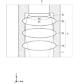
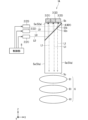
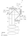
- FIG. 1 is a diagram schematically showing an example of an optical system of a lighting device according to a first embodiment
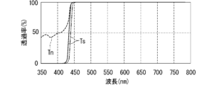
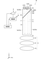
- FIG. FIG. 1 is a cross-sectional view schematically showing an example of the configuration of a lighting device according to a first embodiment. It is a graph which shows an example of the spectral transmittance of a wavelength separation filter.
- FIG. 2 is an enlarged cross-sectional view of a part of the configuration of the lighting device.
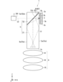
- FIG. 2 is a diagram schematically showing a first aspect of the optical system of the illumination device according to the first embodiment. It is a figure which shows roughly the 2nd aspect of the optical system of the illumination device concerning 1st Embodiment.
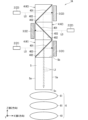
- FIG. 7 is a diagram schematically showing an example of an optical system of a lighting device according to a second embodiment.
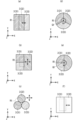
- FIG. 3 is a diagram schematically showing an example of an arrangement of wavelength conversion members.
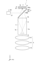
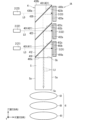
- FIG. 7 is a diagram schematically showing a first aspect of the configuration of a lighting device according to a second embodiment. It is a graph which shows an example of the spectral transmittance of a 3rd wavelength separation filter from a 1st wavelength separation filter. It is a figure which shows roughly the 2nd aspect of the optical system of the illumination device concerning 2nd Embodiment.
- FIG. 3 is a diagram schematically showing an example of an arrangement of wavelength conversion members and an irradiation area of excitation light.
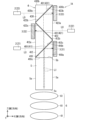
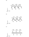
- 1 is a diagram schematically showing an example of the configuration of a lighting device. It is a figure which shows roughly an example of the optical system of the illumination device concerning 4th Embodiment. It is a figure which shows schematically another example of the shape of a wavelength conversion member. It is a figure which shows roughly another aspect of the optical system of the illumination device concerning 4th Embodiment. It is a figure which shows schematically another example of the shape of a wavelength conversion member.
- the inventor has created a technology for emitting more uniform illumination light in a lighting device. Regarding this, the first to fourth embodiments will be described below based on the drawings.
- FIG. 1 is a diagram schematically showing an example of an optical system of a lighting device 1.
- FIG. 2 is a cross-sectional view schematically showing an example of the configuration of the lighting device 1.
- FIG. 1 is a diagram schematically showing an example of an optical system of a lighting device 1.
- FIG. 2 is a cross-sectional view schematically showing an example of the configuration of the lighting device 1.
- FIG. 1 is a diagram schematically showing an example of an optical system of a lighting device 1.
- FIG. 2 is a cross-sectional view schematically showing an example of the configuration of the lighting device 1.
- the illumination device 1 is a device that emits fluorescence L1 as illumination light into the illumination space S1.
- the lighting device 1 is arranged, for example, on the ceiling of the lighting space S1.
- the illumination device 1 includes a light source 2, a wavelength conversion member 3, a wavelength separation filter 4, a light guide member 5, a lens optical system 6, and a housing 7. I'm here. Below, an example of each configuration will first be outlined and then detailed.
- the housing 7 houses the light source 2, the wavelength conversion member 3, the wavelength separation filter 4, the light guide member 5, and the lens optical system 6.
- the casing 7 has a first opening (hereinafter also referred to as an irradiation aperture) 7a at the end on the -Z side, and fluorescence L1 as illumination light is emitted from the irradiation aperture 7a into the illumination space S1.
- the light source 2 has a light emitting section (for example, a light emitting surface) 201 that emits the excitation light L0.
- the excitation light L0 may be light having a peak within a wavelength range from 380 nm to 415 nm.
- the excitation light L0 may be purple light having a peak near 405 nm.
- the excitation light L0 is not necessarily limited to violet light, and may be, for example, blue light having a peak near 450 nm.
- the excitation light L0 from the light source 2 enters the wavelength separation filter 4.
- the wavelength separation filter 4 guides the excitation light L0 to the wavelength conversion member 3.
- the first direction is, for example, the X direction.
- the wavelength conversion member 3 and the wavelength separation filter 4 are arranged along the second direction that intersects the first direction.
- the second direction is, for example, the Z direction.
- the wavelength separation filter 4 reflects the excitation light L0 from the light source 2 toward the wavelength conversion member 3, and guides the excitation light L0 to the wavelength conversion member 3.
- the excitation light L0 enters the wavelength conversion member 3.
- the wavelength conversion member 3 contains a phosphor.
- the wavelength conversion member 3 emits fluorescence L1 based on the incident excitation light L0.
- Fluorescence L1 has a spectrum different from the spectrum of excitation light L0. Specifically, the peak wavelength of the fluorescence L1 is longer than the peak wavelength of the excitation light L0 (hereinafter also referred to as excitation peak wavelength), and the fluorescence L1 is visible light.
- the fluorescence L1 travels from the wavelength conversion member 3 toward the wavelength separation filter 4 and enters the wavelength separation filter 4. In the example of FIGS. 1 and 2, the wavelength separation filter 4 transmits the fluorescence L1 from the wavelength conversion member 3.
- the light guide member 5 has a cylindrical surface 5a.
- the central axis of the cylindrical surface 5a is along the Z direction.
- the fluorescence L1 from the wavelength separation filter 4 travels through the interior surrounded by the cylindrical surface 5a while being repeatedly reflected by the cylindrical surface 5a.
- the fluorescence L1 emitted from the exit surface 5c (described later) of the light guide member 5 advances toward the lens optical system 6 and enters the lens optical system 6.
- the lens optical system 6 includes one or more lenses 61 located between the light guide member 5 and the irradiation aperture 7a. In the example of FIGS. 1 and 2, three lenses 61 are shown. The three lenses 61 are lined up in the Z direction between the light guide member 5 and the irradiation aperture 7a.
- the lens optical system 6 is an imaging optical system that forms an image of the object surface on a virtual image surface IS1 when the exit surface 5c of the light guide member 5 is an object surface.
- the image plane IS1 is located, for example, at the irradiation aperture 7a.
- the fluorescence L1 passes through the irradiation aperture 7a and is irradiated onto the illumination space S1.
- the fluorescence L1 travels inside the light guide member 5 while being reflected by the cylindrical surface 5a of the light guide member 5. Therefore, the intensity distribution of the fluorescence L1 in the cross section (here, the XY cross section) perpendicular to the central axis of the cylindrical surface 5a is made uniform. Therefore, more uniform fluorescence L1 is emitted from the emission surface 5c of the light guide member 5. Consequently, the illumination device 1 can emit more uniform fluorescence L1 as illumination light from the irradiation aperture 7a.
- the lens optical system 6 forms an image on the exit surface 5c of the light guide member 5 on the virtual image plane IS1.
- the fluorescence L1 can be made small on the image plane IS1. Therefore, the fluorescence L1 is less likely to be reflected or scattered on the inner wall of the irradiation opening 7a of the housing 7, and it is possible to realize a more uniform and high-quality illumination space S1 with less glare. Furthermore, the presence of the lighting device 1 when viewed from outside the irradiation aperture 7a can be reduced.
- the light source 2 includes, for example, a semiconductor laser element such as a laser diode (LD), a light emitting element such as a VCSEL (Vertical Cavity Surface Emitting LASER), a light emitting diode (LED), and an SLD (super luminescent diode). May include.
- the emission part 201 of the light source 2 may be the emission end of a light emitting element.
- a gallium nitride (GaN)-based semiconductor laser that emits 405 nm violet laser light as excitation light L0 may be applied to the light emitting element.
- the light source 2 may further include a light guide member such as a fiber and a rod lens in addition to the light emitting element.
- the fiber includes a linear core and a cladding.
- the cladding has a lower refractive index than the core and covers the core.
- the excitation light L0 can be transmitted through the core while being totally reflected at the interface between the core and the cladding.
- the rod lens has, for example, a columnar shape. The excitation light L0 can be transmitted through the inside of the rod lens while being totally reflected on the side surface of the rod lens.
- the input end of such a light guide member corresponds to the first end face of the fiber or the first end face of the rod lens
- the output end of the light guide member corresponds to the second end face of the fiber or the rod lens on the opposite side to the first end face. This corresponds to the second end surface of the lens on the opposite side to the first end surface.
- Excitation light L0 from the light emitting element enters the input end of the light guide member, travels inside the light guide member, and exits from the output end of the light guide member.
- the output portion 201 of the light source 2 corresponds to the output end of the light guide member.
- the light source 2 may emit excitation light L0 having linear polarization.
- the polarization of the excitation light L0 may be, for example, s-polarized light with respect to the incident surface of the wavelength separation filter 4.
- various lenses may be located between the light source 2 and the wavelength separation filter 4.
- Wavelength separation filter 4 In the examples shown in FIGS. 1 and 2, the wavelength separation filter 4 and the light source 2 are spaced apart from each other in the X direction, and are located on the +X side with respect to the light source 2. As described above, the wavelength separation filter 4 guides the excitation light L0 from the light source 2 to the wavelength conversion member 3, and the fluorescence L1 from the wavelength conversion member 3 is incident on the wavelength separation filter 4. In the example of FIGS. 1 and 2, the wavelength separation filter 4 reflects the excitation light L0 toward the wavelength conversion member 3 and transmits the fluorescence L1.
- the wavelength separation filter 4 is also called a dichroic mirror.
- the wavelength separation filter 4 includes, for example, a dielectric multilayer film 401.
- the dielectric multilayer film 401 has a structure in which dielectric thin films are repeatedly stacked multiple times.
- dielectric materials include silicon oxide (SiO 2 ), titanium oxide (TiO 2 ), aluminum oxide (Al 2 O 3 ), zirconium oxide (ZrO 2 ), tantalum oxide (Ta 2 O 5 ), and niobium oxide (Nb 2 O 3 ) are employed.
- the spectral transmittance of the dielectric multilayer film 401 that reflects the excitation light L0 and transmits the fluorescence L1 can be increased. It can be realized. That is, the function of the wavelength separation filter 4 is substantially realized by the dielectric multilayer film 401.
- FIG. 3 is a graph showing an example of the spectral transmittance of the wavelength separation filter 4.
- FIG. 3 shows the transmittance Ts of the wavelength separation filter 4 for s-polarized light and the transmittance Tn of the wavelength separation filter 4 for non-polarized light.
- the polarization state of the excitation light L0 is s-polarized light, and its wavelength is 405 nm.
- the transmittance Ts of the excitation light L0 is almost zero, so the excitation light L0 hardly passes through the wavelength separation filter 4.
- the polarization state of the fluorescence L1 is non-polarized. Since the transmittance Tn in the wavelength range of the fluorescence L1 is approximately 100%, the fluorescence L1 is transmitted through the wavelength separation filter 4.
- the wavelength separation filter 4 is positioned such that the direction along its surface intersects the X direction at an angle of approximately 45 degrees.
- the wavelength separation filter 4 extends from the ⁇ X side and ⁇ Z side toward the +X side and +Z side. Therefore, the traveling direction of the excitation light L0 from the light source 2 changes by about 90 degrees before and after the wavelength separation filter 4. Specifically, the excitation light L0 from the light source 2 travels to the +X side, is reflected by the wavelength separation filter 4, and travels to the +Z side.
- Wavelength conversion member 3 >
- the wavelength conversion member 3 and the wavelength separation filter 4 are arranged at intervals in the Z direction, and are located on the +Z side with respect to the wavelength separation filter 4.
- the wavelength conversion member 3 contains phosphor.
- the wavelength conversion member 3 is made of, for example, BaMgAl 10 O 17 :Eu or (Sr, Ca, Ba) 10 (PO 4 ) as a wavelength conversion material (that is, a fluorescent material) that converts the excitation light L0 into blue light. 6 Cl 2 :Eu, (Sr, Ba) 10 (PO 4 ) 6 Cl 2 :Eu, etc. may be included.
- the wavelength conversion member 3 is a wavelength conversion material that converts the excitation light L0 into blue-green light, such as (Sr, Ba, Ca) 5 (PO 4 ) 3 Cl:Eu, Sr 4 Al 14 O 25 :Eu, etc. may include.
- the wavelength conversion member 3 is made of, for example, SrSi 2 (O, Cl) 2 N 2 :Eu, (Sr, Ba, Mg) 2 SiO 4 :Eu 2+ , as a wavelength conversion material that converts the excitation light L0 into green light.
- SrSi 2 (O, Cl) 2 N 2 :Eu, (Sr, Ba, Mg) 2 SiO 4 :Eu 2+ as a wavelength conversion material that converts the excitation light L0 into green light.
- ZnS:Cu, Al, Zn 2 SiO 4 :Mn, etc. may be included.
- the wavelength conversion member 3 is a wavelength conversion material that converts the excitation light L0 into red light, such as Y 2 O 2 S:Eu, Y 2 O 3 :Eu, SrCaClAlSiN 3 :Eu 2+ , CaAlSiN 3 :Eu, or , CaAlSi(ON) 3 :Eu, and the like.
- the wavelength conversion member 3 may include 3Ga 5 O 12 :Cr or the like as a wavelength conversion material that converts the excitation light L0 into light having a wavelength in the near-infrared region. If the wavelength conversion member 3 includes multiple types of wavelength conversion materials corresponding to multiple colors of light, the wavelength conversion member 3 can emit fluorescence L1 with high color rendering properties.
- the excitation light L0 is light having a peak from 380 nm to 415 nm and the wavelength conversion member 3 has a phosphor corresponding to red, green, and blue light
- the color rendering property of the fluorescence L1 is In particular, it can be enhanced.
- the wavelength conversion member 3 may contain a resin such as a binder for connecting the fine particles of the phosphor to each other.
- the wavelength conversion member 3 has, for example, a surface 3a, a surface 3b, and a side surface 3c.
- the surface 3b is the surface of the wavelength conversion member 3 on the wavelength separation filter 4 side.
- the surface 3a is a surface of the wavelength conversion member 3 on the opposite side to the surface 3b.
- the side surface 3c is a side surface that connects the periphery of the surface 3a and the periphery of the surface 3b of the wavelength conversion member 3.
- the wavelength conversion member 3 may have a plate-like shape. That is, the surface 3a and the surface 3b of the wavelength conversion member 3 are substantially flat surfaces, and may be substantially parallel to each other.
- the wavelength conversion member 3 may be positioned with its thickness direction along the Z direction. That is, the surface 3a and the surface 3b of the wavelength conversion member 3 may be substantially parallel to the XY plane.
- the light guide member 5 may include a first transparent member 51 and a second transparent member 52.
- the material for the first transparent member 51 and the second transparent member 52 for example, at least one of glass such as optical glass and resin such as acrylic resin can be applied.
- a dielectric multilayer film 401 of the wavelength separation filter 4 is located between the first transparent member 51 and the second transparent member 52.
- the first transparent member 51 and the second transparent member 52 also function as base materials that support the dielectric multilayer film 401.
- Such a light guide member 5 is also a rod lens incorporating the wavelength separation filter 4.
- the entire first transparent member 51 and second transparent member 52 may have a columnar shape, for example.
- the light guide member 5 may have a quadrangular prism shape.
- the central axis of the light guide member 5 is, for example, approximately parallel to the Z direction.
- the light guide member 5 has a cylindrical surface 5a, an end surface 5b, and an output surface 5c.
- the end surface 5b and the output surface 5c are end surfaces located on both sides of the light guide member 5 in the longitudinal direction (that is, the Z direction), respectively.
- the exit surface 5c is located on the -Z side, that is, on the lens optical system 6 side with respect to the end surface 5b.
- the cylindrical surface 5a is a side surface that connects the periphery of the end surface 5b and the periphery of the output surface 5c of the light guide member 5.
- the end surface 5b and the output surface 5c may be, for example, flat surfaces, or may be substantially parallel to each other. Further, as shown in FIGS. 1 and 2, the end surface 5b of the light guide member 5 may be substantially parallel to the surface 3b of the wavelength conversion member 3. When the light guide member 5 has a quadrangular prism shape, the end surface 5b and the output surface 5c have a quadrangular shape when viewed along the Z direction.
- the first transparent member 51 and the second transparent member 52 are members obtained by dividing the light guide member 5 into two using the dielectric multilayer film 401 as a boundary.
- the first transparent member 51 has a first side surface 51a that is a part of the cylindrical surface 5a, a first inclined surface 51b, and an output surface 5c.
- the first inclined surface 51b and the output surface 5c are end surfaces located on both sides of the first transparent member 51 in the Z direction, respectively.
- the first inclined surface 51b is inclined to the same extent as the dielectric multilayer film 401 with respect to the X direction.
- the exit surface 5c is located on the lens optical system 6 side with respect to the first inclined surface 51b.
- the first side surface 51a is a side surface that connects the periphery of the first inclined surface 51b and the periphery of the output surface 5c of the first transparent member 51.
- the first transparent member 51 has, for example, a columnar shape in which end faces on both sides in the Y direction are right-angled trapezoids.
- the second transparent member 52 has a second side surface 52a that is the remaining part of the cylindrical surface 5a, an end surface 5b, and a second inclined surface 52c.
- the second inclined surface 52c is inclined to the same extent as the first inclined surface 51b of the first transparent member 51, and faces the first inclined surface 51b.
- the second inclined surface 52c is substantially parallel to the first inclined surface 51b.
- the +X side end of the second inclined surface 52c is connected to the +X side end of the end surface 5b.
- the second side surface 52a is a side surface that connects the end surface 5b of the second transparent member 52 and the second inclined surface 52c.
- the second transparent member 52 has, for example, a columnar shape in which end faces on both sides in the Y direction are right triangles.
- the dielectric multilayer film 401 of the wavelength separation filter 4 is located between the first inclined surface 51b of the first transparent member 51 and the second inclined surface 52c of the second transparent member 52. In other words, the first inclined surface 51b and the second inclined surface 52c sandwich the dielectric multilayer film 401.
- the dielectric multilayer film 401 is formed on one of the first inclined surface 51b and the second inclined surface 52c.
- the dielectric multilayer film 401 is formed by a physical vapor deposition method such as a vacuum evaporation method, a sputtering method, an ion plating method, or a chemical vapor deposition method (CVD method).
- the first transparent member 51 and the second transparent member 52 may be fixed to each other via a fixing agent such as a transparent adhesive, for example.
- a fixing agent such as a transparent adhesive
- the dielectric multilayer film 401 is formed on one of the first slope surface 51b and the second slope surface 52c, and the adhesive is applied to the other of the first slope surface 51b and the second slope surface 52c and the dielectric multilayer film 401.
- a resin such as a photocurable resin can be used as the adhesive.
- the excitation light L0 from the light source 2 enters the second side surface 52a of the second transparent member 52, and travels inside the second transparent member 52 from the second side surface 52a toward the wavelength separation filter 4.
- the excitation light L0 is reflected by the wavelength separation filter 4 and travels inside the second transparent member 52 toward the end surface 5b.
- the excitation light L0 is emitted toward the wavelength conversion member 3 from the end surface 5b and is incident on the surface 3b of the wavelength conversion member 3. That is, the end surface 5b can function as an exit surface for the excitation light L0.
- the fluorescence L1 from the wavelength conversion member 3 travels toward the second transparent member 52 while spreading, and enters the end surface 5b of the second transparent member 52.
- the fluorescent light L1 is refracted at the end surface 5b and travels inside the second transparent member 52 toward the wavelength separation filter 4.
- the end surface 5b also functions as an incident surface for the fluorescence L1. Due to the refraction at the end surface 5b, the spread angle of the fluorescence L1 becomes smaller. In other words, the end surface 5b can function as an end surface of a condensing lens.
- the fluorescence L1 passes through the wavelength separation filter 4 and travels inside the first transparent member 51 toward the exit surface 5c.
- the fluorescence L1 is emitted toward the lens optical system 6 from the emission surface 5c.
- the fluorescent light L1 is repeatedly reflected on the cylindrical surface 5a of the light guide member 5 while traveling from the end surface 5b toward the output surface 5c.
- the intensity distribution of the fluorescence L1 in a cross section perpendicular to the longitudinal direction (here, the Z direction) of the light guide member 5 is made uniform. Therefore, more uniform fluorescence L1 is emitted from the emission surface 5c of the light guide member 5. Moreover, color unevenness of the fluorescent light L1 on the emission surface 5c can also be reduced.
- the length of the light guide member 5 in the Z direction may be, for example, 10 mm or more.
- the first transparent member 51 from the wavelength separation filter 4 to the output surface 5c is integral.
- integrated object means, for example, an object made of a single member without having a plurality of members. If the first transparent member 51 is integrated, there will be no boundary surface (adhesive surface) between different members in the region from the wavelength separation filter 4 to the output surface 5c. Therefore, the loss of the fluorescence L1 can be reduced, and the lighting device 1 can emit the fluorescence L1 into the illumination space S1 with higher efficiency.
- the area of the end surface 5b of the light guide member 5 may be greater than or equal to the area of the surface 3b of the wavelength conversion member 3.
- the diagonal of the surface 3b may be approximately 2 mm to 4 mm
- the diagonal of the end surface 5b may be approximately 2 mm to 4 mm.
- the illumination device 1 can emit the fluorescence L1 into the illumination space S1 with higher efficiency.
- the wavelength conversion member 3 and the second transparent member 52 may be separated from each other.
- the first distance between the surface 3b of the wavelength conversion member 3 and the end surface 5b of the second transparent member 52 may be narrower than the second distance between the lens optical system 6 and the irradiation aperture 7a, for example.
- the second interval is, for example, the interval between the lens 61 of the lens optical system 6 that is closest to the irradiation aperture 7a and the irradiation aperture 7a.
- the first interval can be, for example, 5 mm or less.
- the second interval can be, for example, 10 mm or more. If the first interval is narrower, more light of the fluorescent light L1 that spreads and travels from the wavelength conversion member 3 can be made to enter the end surface 5b of the second transparent member 52.
- no other optical element for example, a lens
- a lens may be located between the wavelength conversion member 3 and the second transparent member 52. According to this, it is easy to set the first interval between the wavelength conversion member 3 and the second transparent member 52 to be narrow.
- Lens optical system 6 In the examples shown in FIGS. 1 and 2, the lens optical system 6 is lined up with an interval from the light guide member 5 in the Z direction, and is located on the ⁇ Z side with respect to the light guide member 5.
- the lens 61 of the lens optical system 6 is located between the output surface 5c of the light guide member 5 and the irradiation aperture 7a of the housing 7.
- the lens 61 is formed of a material containing at least one of glass such as optical glass and resin such as acrylic resin, for example.
- each lens 61 may be a biconvex lens, for example.
- the optical axis of the lens 61 is along the Z direction.
- the Z direction is the optical axis direction of the lens optical system 6.
- the lens 61 is not limited to a convex lens, but may be a concave lens or a meniscus lens. Further, the lens 61 may be a spherical lens or an aspherical lens.
- the lens optical system 6 is an imaging optical system that forms an image of the object surface on a virtual image surface IS1 when the exit surface 5c of the light guide member 5 is an object surface. That is, in the example of FIGS. 1 and 2, three lenses 61 constitute the imaging optical system.
- the lens 61 (particularly the lens 61 closest to the irradiation aperture 7a) may also be called an imaging lens.
- the output surface 5c of the light guide member 5 has a conjugate relationship with the image plane IS1.
- conjugate relationship does not have a strict meaning, but rather refers to the part where the fluorescence L1 is most concentrated (perpendicular to the optical axis of the lens optical system 6) on the irradiation aperture 7a side from the exit surface 5c of the light guide member 5.
- the portion in the cross section where the size of the fluorescence L1 is smallest can be regarded as the image plane IS1.
- the image plane IS1 may be located at the irradiation aperture 7a, for example.
- the image surface IS1 may be a flat surface or a curved surface.
- the fluorescence L1 is focused on the image plane IS1 and is emitted into the illumination space S1 through the illumination aperture 7a.
- the image plane IS1 does not necessarily need to be located inside the irradiation aperture 7a.
- the image plane IS1 may be located slightly shifted from the irradiation aperture 7a in the traveling direction (here, Z direction) of the fluorescence L1 passing through the irradiation aperture 7a. That is, the image plane IS1 may be located slightly inside the housing 7 than the irradiation aperture 7a, or may be located slightly on the illumination space S1 side.
- the size M1 of the fluorescence L1 on the output surface 5c of the light guide member 5 may be, for example, the size of the output surface 5c of the light guide member 5 itself.
- the size M3 of the irradiation aperture 7a is the opening area of the irradiation aperture 7a viewed along the Z direction.
- the diameter or diagonal length of the irradiation aperture 7a may be, for example, about 5 mm to 15 mm. .
- the size M3 of the irradiation aperture 7a is different at each position in the Z direction. In this case, for example, the minimum value can be adopted as the size M3 of the irradiation aperture 7a.
- Imaging magnification is the ratio of the size M2 of the fluorescence L1 on the image plane IS1 to the size M1 of the fluorescence L1 on the exit surface 5c of the light guide member 5.
- the size of the fluorescence L1 may be defined by a contour line having a light amount e 1/2 of the peak value in the light amount distribution of the fluorescence L1 in a cross section perpendicular to the Z direction.
- e is called Napier's number.
- the light rays on both sides of the fluorescence L1 in FIG. 2 may be light rays having a light intensity that is e 1/2 of the peak value of the light intensity distribution in a cross section perpendicular to the optical axis AX1.
- Light in a region outside the region surrounded by the above contour lines that is, both outer rays
- the size M2 of the fluorescence L1 on the image plane IS1 can be made equal to or less than the size M3 of the irradiation aperture 7a. Therefore, it is possible to reduce the possibility that the fluorescence L1 will enter the peripheral portion of the irradiation opening 7a of the housing 7. Thereby, unnecessary reflected and scattered light leaking from the irradiation aperture 7a can be reduced.
- the imaging magnification of the lens optical system 6 may be set so that the size of the fluorescence L1 passing through the irradiation aperture 7a is smaller than that of the irradiation aperture 7a. According to this, reflected and scattered light can be further reduced.
- FIG. 4 is an enlarged cross-sectional view of a part of the configuration of the lighting device 1.
- the spread angle ⁇ 1 of the fluorescence L1 from the output surface 5c of the light guide member 5 may be equal to or less than the angle ⁇ 1 that defines the numerical aperture of the lens optical system 6.
- the numerical aperture is the product of the sine of the half value of the angle ⁇ 1 and the refractive index.
- the angle ⁇ 1 here is, for example, an angle formed by both outer rays of virtual light passing through the effective area of the lens optical system 6.
- the effective area here corresponds to a light passage area where the optical performance of the lens optical system 6 can be exhibited.
- the effective area of the lens 61 is an area of the lens 61 excluding a predetermined peripheral width.
- the effective area of the lens 61 may be an area surrounded by the inner periphery of a portion of the housing 7 (that is, a lens holder) that holds the periphery of the lens 61.
- the fluorescence L1 can pass through the effective area of the lens optical system 6. Therefore, almost no fluorescence L1 enters the edge of the lens 61, and unnecessary reflection and scattering of the fluorescence L1 occurring at the edge can be suppressed or avoided.
- the imaging magnification of the lens optical system 6 may be less than or equal to the above ratio, and the spread angle ⁇ 1 may be less than or equal to the angle ⁇ 1. According to this, unnecessary reflection and scattering of the fluorescence L1 at the periphery of the lens optical system 6 and the irradiation aperture 7a can be suppressed or avoided. Therefore, the illumination device 1 can emit most of the fluorescence L1 from the light guide member 5 into the illumination space S1 through the irradiation opening 7a. In other words, it is possible to improve the amount of fluorescent light L1 emitted into the illumination space S1.
- the lighting device 1 can irradiate the illumination space S1 with highly efficient and high quality fluorescent light L1.
- the spread angle ⁇ 2 (see FIG. 2) of the fluorescence L1 in the illumination space S1 may be smaller than the spread angle ⁇ 1 of the fluorescence L1 that enters the lens optical system 6 from the exit surface 5c of the light guide member 5.
- the lens optical system 6 may be designed such that the spread angle ⁇ 2 is smaller than the spread angle ⁇ 1.
- the orientation angle (eg, half-value angle) of the fluorescence L1 in the illumination space S1 is, for example, about 60 degrees or less.
- the orientation angle of the lighting device 1 may be less than 45 degrees, less than 30 degrees or less than 15 degrees, for example.
- the illumination space S1 in which a plurality of illumination devices 1 are installed at regular intervals glare from the illumination devices 1 that enter the field of view can be reduced. As a result, the comfort of the illumination space S1 can be improved.
- FIG. 5 is a diagram schematically showing a first aspect of the optical system of the illumination device 1 according to the first embodiment.
- the light source 2, wavelength separation filter 4, and wavelength conversion member 3 may be arranged in the X direction.
- the light source 2 is located on the ⁇ X side with respect to the wavelength separation filter 4
- the wavelength conversion member 3 is located on the +X side with respect to the wavelength separation filter 4. Therefore, in this structure, the wavelength separation filter 4 transmits the excitation light L0 from the light source 2 to the wavelength conversion member 3 side.
- the excitation light L0 that has passed through the wavelength separation filter 4 enters the wavelength conversion member 3.
- the fluorescence L1 emitted by the wavelength conversion member 3 advances toward the wavelength separation filter 4 and enters the wavelength separation filter 4.
- the wavelength separation filter 4 reflects the fluorescence L1 toward the ⁇ Z side.
- the fluorescence L1 reflected by the wavelength separation filter 4 travels inside the light guide member 5 toward the output surface 5c while being repeatedly reflected by the cylindrical surface 5a of the light guide member 5.
- FIG. 6 is a diagram schematically showing a second aspect of the optical system of the illumination device 1 according to the first embodiment.
- the wavelength separation filter 4 may include a dichroic prism incorporating a dielectric multilayer film 401.
- the wavelength separation filter 4 includes a dielectric multilayer film 401, a first prism 402, and a second prism 403.
- the material for the first prism 402 and the second prism 403 for example, at least one of glass such as optical glass and resin such as acrylic resin can be used.
- the second prism 403 has a side surface 403a, an end surface 403b, and a second inclined surface 403c.
- the second prism 403 may have the same shape as the second transparent member 52 in FIG. That is, the side surface 403a is the same as the second side surface 52a of the second transparent member 52, the end surface 403b is the same as the end surface 5b of the second transparent member 52, and the second inclined surface 403c is the same as the second side surface 52a of the second transparent member 52. It may be the same as the inclined surface 52c.
- the second prism 403 has, for example, a right triangular prism shape in which end faces on both sides in the Y direction are right triangles. In the example of FIG. 6, the end surface 403b of the second prism 403 faces the surface 3b of the wavelength conversion member 3 in the Z direction.
- the first prism 402 has a side surface 402a, a first inclined surface 402b, and an end surface 402c.
- the first inclined surface 402b is inclined to the same extent as the second inclined surface 403c of the second prism 403, and faces the second inclined surface 403c.
- the first inclined surface 402b is approximately parallel to the second inclined surface 403c.
- the end surface 402c is located on the light guide member 5 side with respect to the first inclined surface 402b.
- the end surface 402c may be a flat surface substantially parallel to the XY plane. In the example of FIG. 6, the ⁇ X side end of the end surface 402c is connected to the ⁇ X side end of the first inclined surface 402b.
- the side surface 402a is a side surface that connects the first inclined surface 402b and the end surface 402c of the first prism 402.
- the first prism 402 has a right triangular prism shape with right triangular end faces on both sides in the Y direction.
- the dielectric multilayer film 401 is located between the first inclined surface 402b of the first prism 402 and the second inclined surface 403c of the second prism 403.
- the dielectric multilayer film 401 is formed on one of the first inclined surface 402b and the second inclined surface 403c.
- the first prism 402 and the second prism 403 may be fixed to each other via a fixing agent such as a transparent adhesive, for example.
- the adhesive may be located between the dielectric multilayer film 401 and the other of the first inclined surface 402b and the second inclined surface 403c.
- Such a wavelength separation filter 4 corresponds to a member having the dielectric multilayer film 401 among the members obtained by dividing the light guide member 5 in FIG. 1 into two in the XY cross section.
- the light guide member 5 includes a rod lens having a columnar shape.
- the end surface 5b of the light guide member 5 (that is, the rod lens) is located apart from the wavelength separation filter 4 in the Z direction.
- the end surface 5b of the light guide member 5 faces the end surface 402c of the first prism 402, and is, for example, substantially parallel to the end surface 402c.
- the fluorescence L1 from the wavelength separation filter 4 is incident on the end surface 5b of the light guide member 5.
- the exit surface 5c is a surface of the light guide member 5 on the opposite side to the end surface 5b, that is, the surface on the lens optical system 6 side.
- the output surface 5c is, for example, approximately parallel to the end surface 5b.
- the cylindrical surface 5a of the light guide member 5 is a side surface that connects the periphery of the end surface 5b and the periphery of the output surface 5c.
- the wavelength separation filter 4 may be fixed to the light guide member 5 via a fixing agent such as a transparent adhesive, for example.
- the adhesive may be located between the end surface 402c of the first prism 402 and the end surface 5b of the light guide member 5.
- the dichroic prism that is the wavelength separation filter 4 according to the second embodiment is already existing, and the rod lens that is the light guide member 5 is also existing. That is, the existing wavelength separation filter 4 and light guide member 5 can be used in the lighting device 1. Therefore, the manufacturing cost of the lighting device 1 according to the second aspect can be reduced.
- the area of the end surface 403b of the second prism 403 may be greater than or equal to the area of the surface 3b of the wavelength conversion member 3.
- the first distance between the end surface 403b of the second prism 403 and the surface 3b of the wavelength conversion member 3 may be narrower than the second distance between the lens optical system 6 and the irradiation aperture 7a, for example. According to this, more light of the fluorescence L1 from the wavelength conversion member 3 can be made to enter the end surface 403b of the second prism 403.
- FIG. 7 is a diagram schematically showing a third aspect of the optical system of the illumination device 1 according to the first embodiment.
- the wavelength separation filter 4 may have a plate-like shape.
- the wavelength separation filter 4 includes a dielectric multilayer film 401 and a transparent base material 404.
- the material of the transparent base material 404 for example, at least one of glass such as optical glass and resin such as acrylic resin can be used.
- the transparent base material 404 and the light guide member 5 are arranged at intervals in the Z direction.
- the transparent base material 404 has a plate-like shape and has a surface 404a (corresponding to the first surface) and a surface 404b (corresponding to the second surface).
- the surface 404b is the surface of the transparent base material 404 on the opposite side to the surface 404a.
- Surface 404a and surface 404b are substantially parallel to each other and inclined at approximately 45 degrees to the X direction.
- Dielectric multilayer film 401 is located, for example, on surface 404a or surface 404b of transparent base material 404.
- the dielectric multilayer film 401 is located on the plate-shaped transparent base material 404. Therefore, the volume of the transparent member can be small, and the manufacturing cost of the wavelength separation filter 4 can be reduced.
- a condensing lens may be located between the wavelength separation filter 4 and the wavelength conversion member 3. Fluorescence L1 from the wavelength conversion member 3 enters the wavelength separation filter 4 through a condensing lens. Thereby, more of the fluorescence L1 from the wavelength conversion member 3 can be made to enter the wavelength separation filter 4.
- the light guide member 5 is a so-called rod lens, but its shape may be changed as appropriate.
- the light guide member 5 may have a prismatic shape such as a triangular prism, a quadrangular prism, a pentagonal prism, and a hexagonal prism, or may have a cylindrical shape.
- the light guide member 5 is not limited to a rod lens, but may be another type of light guide member.
- the light guiding member 5 may be a fiber.
- the fiber includes a linear core and a cladding.
- the cladding has a lower refractive index than the core and covers the core.
- the fluorescence L1 can be transmitted through the core while being totally reflected on the cylindrical surface that is the interface between the core and the cladding. Even when the light guide member 5 is a fiber, the dielectric multilayer film 401 of the wavelength separation filter 4 may be incorporated therein.
- the light guide member 5 may be, for example, a lens barrel.
- the lens barrel has a cylindrical shape, and the cylindrical surface that is the inner peripheral surface thereof has reflective properties.
- the fluorescence L1 can pass through the inside of the lens barrel while being totally reflected on the inner peripheral surface of the lens barrel.
- the light guide member 5 may have a rectangular tube shape such as a triangular tube shape, a square tube shape, a pentagonal tube shape, a hexagonal tube shape, etc., or a cylindrical shape. You can.
- FIG. 8 is a diagram schematically showing an example of the optical system of the illumination device 1A according to the second embodiment.
- the lighting device 1A according to the second embodiment is different from the lighting device 1 according to the first embodiment in terms of the number of wavelength conversion members 3 and light sources 2.
- a plurality of wavelength conversion members 3 are located.
- a first wavelength conversion member 31, a second wavelength conversion member 32, and a third wavelength conversion member 33 are shown as the plurality of wavelength conversion members 3.
- the first to third wavelength conversion members 31 to 33 emit fluorescence L1 having different spectra from each other.
- the first wavelength conversion member 31 includes a first color phosphor and emits the first color fluorescence L1.
- the first color is, for example, red.
- the second wavelength conversion member 32 includes, for example, a second color phosphor and emits second color fluorescence L1.
- the second color is, for example, green.
- the third wavelength conversion member 33 includes, for example, a third color phosphor and emits third color fluorescence L1.
- the third color is, for example, blue.
- the structure including the first to third wavelength conversion members 31 to 33 may face the wavelength separation filter 4 in the Z direction.
- the structure faces the end surface 5b of the light guide member 5 in the Z direction.
- the first wavelength conversion member 31 to the third wavelength conversion member 33 are lined up in this order in the X direction.
- the first wavelength conversion member 31 is located closest to the -X side
- the third wavelength conversion member 33 is located closest to the +X side.
- the first wavelength conversion member 31 may be adjacent to and in contact with the second wavelength conversion member 32
- the second wavelength conversion member 32 may be adjacent to and in contact with the third wavelength conversion member 33.
- the first to third wavelength conversion members 31 to 33 correspond to, for example, members obtained by dividing the wavelength conversion member 3 in FIG. 1 into three equal parts in the X direction.
- a plurality of light sources 2 may be located in one-to-one correspondence with a plurality of wavelength conversion members 3.
- the plurality of light sources 2 include a first light source 21, a second light source 22, and a third light source 23.
- the structure including the first light source 21 to the third light source 23 may be aligned with the wavelength separation filter 4 in the X direction.
- the first light source 21 to the third light source 23 may be arranged in the Z direction.
- the first light source 21 is located closest to the ⁇ Z side
- the third light source 23 is located closest to the +Z side.
- the excitation light L0 emitted by the first light source 21 enters the wavelength separation filter 4, and is guided to the first wavelength conversion member 31 by the wavelength separation filter 4.
- the excitation light L0 from the first light source 21 is incident on the second side surface 52a of the second transparent member 52, and from the second side surface 52a, the inside of the second transparent member 52 is directed toward the wavelength separation filter 4. move on.
- the excitation light L0 is reflected by the wavelength separation filter 4 and travels inside the second transparent member 52 toward the end surface 5b.
- the excitation light L0 travels toward the first wavelength conversion member 31 from the end surface 5b and enters the first wavelength conversion member 31.
- the excitation light L0 emitted by the second light source 22 enters the wavelength separation filter 4 and is guided by the wavelength separation filter 4 to the second wavelength conversion member 32.
- the excitation light L0 emitted by the third light source 23 enters the wavelength separation filter 4 and is guided by the wavelength separation filter 4 to the third wavelength conversion member 33.
- the first wavelength conversion member 31 emits the first color of fluorescence L1 based on the excitation light L0 that has entered itself.
- the second wavelength conversion member 32 emits second color fluorescence L1 based on the excitation light L0 that has entered itself.
- the third wavelength conversion member 33 emits third color fluorescence L1 based on the excitation light L0 that has entered itself.
- the fluorescence L1 emitted from the first wavelength converting member 31 to the third wavelength converting member 33 respectively advances toward the end surface 5b of the second transparent member 52 while spreading, and enters the end surface 5b of the second transparent member 52.
- These fluorescent lights L1 are refracted at the end surface 5b and travel inside the second transparent member 52 toward the wavelength separation filter 4.
- the fluorescence L1 passes through the wavelength separation filter 4 and travels inside the first transparent member 51 toward the exit surface 5c. Since the fluorescent light L1 travels inside the light guide member 5 toward the exit surface 5c while being repeatedly reflected on the cylindrical surface 5a, the first to third colors of fluorescent light L1 are spatially mixed. Therefore, the fluorescent light L1, which is a mixture of the first to third colors, is emitted from the emission surface 5c of the light guide member 5. Therefore, the illumination device 1A can emit the fluorescent light L1, which is a mixture of the first to third colors, from the irradiation opening 7a.
- the first light source 21 to the third light source 23 may each emit excitation light L0 with a variable amount of light.
- the first light source 21 includes a first light emitting element such as an LD, a VCSEL, an SLD, and an LED, and a first drive circuit that drives the first light emitting element.
- the first drive circuit includes, for example, a switching power supply circuit, and supplies variable power to the first light emitting element.
- the first light emitting element emits excitation light L0 based on the electric power.
- the second light source 22 also includes a second light emitting element and a second drive circuit
- the third light source 23 also includes a third light emitting element and a third drive circuit.
- the first light source 21, the second light source 22, and the third light source 23 are controlled by the control unit 8.
- a control board or a microcomputer is applied to the control unit 8.
- a large-scale integrated circuit (LSI) in which a central processing unit (CPU), memory, and the like are integrated is applied to the microcomputer.
- LSI large-scale integrated circuit
- the control unit 8 can also be called a control circuit. Controller 8 includes at least one processor to provide control and processing capabilities to perform various functions, as described in further detail below.
- At least one processor may be implemented as a single integrated circuit (IC) or as a plurality of communicatively connected integrated circuits and/or discrete circuits. good.
- the at least one processor can be implemented according to various known techniques.
- a processor includes one or more circuits or units configured to perform one or more data calculation procedures or processes, for example, by executing instructions stored in an associated memory.
- the processor may be firmware (eg, a discrete logic component) configured to perform one or more data calculation procedures or processes.
- the processor is one or more processors, controllers, microprocessors, microcontrollers, application specific integrated circuits (ASICs), digital signal processing equipment, programmable logic devices, field programmable gate arrays, or any of the foregoing. It may include any combination of devices or configurations, or other known combinations of devices and configurations, to perform the functions described below.
- ASICs application specific integrated circuits
- control unit 8 all the functions of the control unit 8 or some of the functions of the control unit 8 may be realized by a hardware circuit that does not require software to realize the functions.
- the control unit 8 can individually output control signals to the first drive circuit, the second drive circuit, and the third drive circuit.
- the control signal is a signal corresponding to a target value of the amount of excitation light L0 emitted from the first light source 21, the second light source 22, and the third light source 23.
- the control unit 8 may control the operation of the first drive circuit, for example, in response to a signal from an external device (for example, a lighting switch) of the lighting device 1A.
- the control unit 8 receives a signal regarding the target value of the excitation light L0 from an external device, and outputs a control signal according to the signal to the first drive circuit.
- the first drive circuit drives the first light emitting element based on the control signal, and causes the first light emitting element to emit excitation light L0 having a light intensity near the target value. Further, the control unit 8 can control the operations of the second drive circuit and the third drive circuit, similarly to the first drive circuit.
- control unit 8 can individually adjust the amount of fluorescence L1 emitted from the first wavelength conversion member 31 to the third wavelength conversion member 33. That is, among the fluorescence L1 emitted by the illumination device 1A, the proportions of the first color fluorescence L1, the second color fluorescence L1, and the third color fluorescence L1 can be changed. According to this, the illumination device 1A can adjust the color of the fluorescence L1 emitted into the illumination space S1.
- a single wavelength separation filter 4 is located with respect to the plurality of wavelength conversion members 31. Therefore, compared to a structure in which a plurality of wavelength separation filters 4 corresponding to a plurality of wavelength conversion members 31 are used, the manufacturing cost of the illumination device 1A can be reduced.
- FIG. 9 is a diagram schematically showing an example of the arrangement of the wavelength conversion members 3.
- FIG. 9 illustrates the shape of the wavelength conversion member 3 viewed along the Z direction.
- each of the first wavelength conversion member 31, the second wavelength conversion member 32, and the third wavelength conversion member 33 has a rectangular shape when viewed along the Z direction. You can leave it there.
- the first to third wavelength conversion members 31 to 33 are arranged in this order in the short direction.
- the lateral direction is the X direction.
- the second wavelength conversion member 32 may be adjacent to and in contact with the first wavelength conversion member 31 and the third wavelength conversion member 33.
- the structure including the first to third wavelength conversion members 31 to 33 has a rectangular shape.
- the first to third wavelength conversion members 31 to 33 may have approximately the same area or may have the same shape.
- the areas of the first wavelength conversion member 31, the second wavelength conversion member 32, and the third wavelength conversion member 33 may be different.
- the area of the second wavelength conversion member 32 that emits the second color (here, green) fluorescence L1 may be larger than the area of both the first wavelength conversion member 31 and the third wavelength conversion member 33. Since the visibility of green is high, if the second wavelength conversion member 32 that emits green fluorescence L1 as the second color has a large area, the illumination device 1 can emit the fluorescence L1 with higher brightness.
- the first wavelength conversion member 31 and the third wavelength conversion member 33 may have approximately the same area and may have the same rectangular shape. Good too. In the example of FIG.
- the first wavelength conversion member 31 and the third wavelength conversion member 33 are adjacent to each other in the Y direction, and the second wavelength conversion member 32 is in contact with the first wavelength conversion member 31. and the third wavelength conversion member 33, for example, in adjacent contact with each other in the X direction.
- the second wavelength conversion member 32 may have the same rectangular shape as the overall shape of the first wavelength conversion member 31 and the third wavelength conversion member 33. Also in the example of FIG. 9(b), the structure including the first to third wavelength conversion members 31 to 33 has a rectangular shape.
- the area of the wavelength conversion member 3 containing a fluorescent material having low resistance to heat is made larger than the area of the wavelength conversion member 3 containing a fluorescent material having higher resistance to heat than the fluorescent material. You may.
- the excitation light L0 can be incident on the wavelength conversion member 3, which has a large area and low heat resistance, over a wider irradiation area. Therefore, even if the power density of the excitation light L0 to the wavelength converter 3 is reduced, the wavelength converter 3 can still emit fluorescence L1 with a sufficient amount of light. Then, by reducing the power density of the excitation light L0, the temperature rise of the wavelength conversion member 3 can be alleviated.
- the wavelength conversion member 3 having low heat resistance can emit the fluorescence L1 with high reliability.
- the amount of fluorescent material can be reduced, and the manufacturing cost of the lighting device 1A can be reduced.
- the excitation light L0 can be made to enter the second wavelength conversion member 32 over a wider range. Therefore, it is possible to realize the illumination device 1A suitable for a situation where the second color fluorescent light L1 is used frequently.
- each of the first to third wavelength conversion members 31 to 33 may have a circular shape.
- the first to third wavelength conversion members 31 to 33 may be circumscribed with each other.
- the first to third wavelength conversion members 31 to 33 have approximately the same area.
- each of the first to third wavelength conversion members 31 to 33 may have a fan-like shape.
- the first to third wavelength conversion members 31 to 33 have approximately the same area and have a central angle of about 120 degrees.
- the first to third wavelength conversion members 31 to 33 are adjacent to each other and in contact with each other with their respective centers coincident.
- the structure including the first wavelength conversion member 31 to the third wavelength conversion member 33 has a circular shape. That is, the first to third wavelength conversion members 31 to 33 have shapes obtained by dividing a circle into three equal parts in the circumferential direction.
- the areas of the first to third wavelength conversion members 31 to 33 may be different.
- the area of the second wavelength conversion member 32 that emits the second color (here, green) fluorescence L1 may be larger than the area of both the first wavelength conversion member 31 and the third wavelength conversion member 33.
- the second wavelength conversion member 32 has a semicircular shape, and the first wavelength conversion member 31 and the third wavelength conversion member 33 are arranged in a fan having a central angle of about 90 degrees. It has the shape of a shape.
- the structure including the first to third wavelength conversion members 31 to 33 has a circular shape.
- a first wavelength conversion member 31 and a second wavelength conversion member 32 may be located as the plurality of wavelength conversion members 3.
- the first wavelength conversion member 31 includes, for example, a phosphor that is a mixture of multiple types of phosphors.
- the first wavelength conversion member 31 emits fluorescence L1 having a first color temperature according to the characteristics and mixing ratio of multiple types of phosphors. For example, 2650 Kelvin (K) is applied to the first color temperature.
- the second wavelength conversion member 32 also includes, for example, a phosphor in which a plurality of types of phosphors are mixed.
- the second wavelength conversion member 32 emits fluorescence L1 of a second color temperature according to the characteristics and mixing ratio of multiple types of fluorescent substances. For example, 6500K is applied to the second color temperature. Note that various color temperatures such as 3000K, 4000K, or 5000K may be applied to the first color temperature or the second color temperature, for example.
- the first wavelength conversion member 31 and the second wavelength conversion member 32 have a rectangular shape, and are in contact with each other in the short direction (here, the X direction). They are lined up.
- the structure including the first wavelength conversion member 31 and the second wavelength conversion member 32 has a rectangular shape.
- the first light source 21 corresponding to the first wavelength conversion member 31 and the second light source 22 corresponding to the second wavelength conversion member 32 are located. In other words, the third light source 23 is unnecessary.
- FIG. 10 is a diagram schematically showing a first aspect of the configuration of a lighting device 1A according to the second embodiment.
- a plurality of wavelength separation filters 4 are located in one-to-one correspondence with a plurality of wavelength conversion members 3.
- the plurality of wavelength separation filters 4 include a first wavelength separation filter 41 and a second wavelength separation filter corresponding to the first wavelength conversion member 31, the second wavelength conversion member 32, and the third wavelength conversion member 33, respectively. 42 and a third wavelength separation filter 43 are located.
- Each of the first to third wavelength separation filters 41 to 43 may be, for example, a dichroic prism, and specifically includes a dielectric multilayer film 401, a first prism 402, and a second prism 403. But that's fine.
- the first light source 21, the first wavelength separation filter 41, and the first wavelength conversion member 31 are lined up in the first direction (here, the X direction), and the second light source 22, the second wavelength separation filter 42 and the second wavelength conversion member 32 are lined up in the X direction, and the third light source 23, the third wavelength separation filter 43, and the third wavelength conversion member 33 are lined up in the X direction.
- the light guide member 5 and the first to third wavelength separation filters 41 to 43 are lined up in the second direction (here, the Z direction). Further, the first to third wavelength separation filters 41 to 43 are arranged in this order as they move away from the light guide member 5 in the Z direction. That is, the first wavelength separation filter 41 is located at the closest position to the light guide member 5, and the third wavelength separation filter 43 is located at the farthest position from the light guide member 5. In other words, the shorter the peak wavelength of the fluorescence L1 emitted by the wavelength conversion member 3, the farther the corresponding wavelength separation filter 4 is located from the light guide member 5.
- the third wavelength separation filter 43 corresponding to the third wavelength conversion member 33 that emits the third color of fluorescence L1 having the shortest peak wavelength is located at the farthest position from the light guide member 5.
- the light guide member 5 and the first to third wavelength separation filters 41 to 43 may be fixed to each other with a fixing agent such as an adhesive, for example.
- the third wavelength separation filter 43 guides the excitation light L0 from the third light source 23 to the third wavelength conversion member 33 side, and also directs the third color fluorescence L1 from the third wavelength conversion member 33 to the second wavelength separation filter 43. lead to the side. Specifically, the third wavelength separation filter 43 transmits the excitation light L0 from the third light source 23 to the +X side, that is, to the third wavelength conversion member 33 side. On the other hand, the third wavelength separation filter 43 reflects the third color fluorescence L1 from the third wavelength conversion member 33 to the -Z side, that is, to the second wavelength separation filter 42 side.
- the second wavelength separation filter 42 guides the excitation light L0 from the second light source 22 to the second wavelength conversion member 32, and also guides the third color fluorescence L1 from the third wavelength separation filter 43 and the excitation light L0 from the second wavelength conversion member 32. Both of the second color fluorescence L1 are guided to the first wavelength separation filter 41. Specifically, the second wavelength separation filter 42 transmits the excitation light L0 from the second light source 22 to the +X side, that is, to the second wavelength conversion member 32 side, and extracts the third color from the third wavelength separation filter 43. The fluorescence L1 is transmitted to the ⁇ Z side, that is, to the first wavelength separation filter 41 side. Further, the second wavelength separation filter 42 reflects the second color fluorescence L1 from the second wavelength conversion member 32 toward the first wavelength separation filter 41 side.
- the first wavelength separation filter 41 guides the excitation light L0 from the first light source 21 to the first wavelength conversion member 31, and also guides the excitation light L0 from the first light source 21 to the first wavelength conversion member 31.
- the first color fluorescence L1 from the conversion member 31 is guided to the light guide member 5.
- the first wavelength separation filter 41 transmits the excitation light L0 from the first light source 21 to the +X side, that is, to the first wavelength conversion member 31 side, and transmits the second color and the excitation light L0 from the second wavelength separation filter 42.
- the third color fluorescence L1 is transmitted to the ⁇ Z side, that is, to the light guide member 5 side.
- the first wavelength separation filter 41 reflects the first color fluorescence L1 from the first wavelength conversion member 31 toward the light guide member 5 side.
- FIG. 11 is a graph showing an example of the spectral transmittance of the first to third wavelength separation filters 41 to 43.
- the spectral transmittance T41 of the dielectric multilayer film 401 of the first wavelength separation filter 41 the spectral transmittance T42 of the dielectric multilayer film 401 of the second wavelength separation filter 42, and the dielectric The spectral transmittance T43 of the body multilayer film 401 is shown.
- the "light source wavelength" shown in FIG. 11 indicates, for example, the excitation peak wavelength of the excitation light L0
- the "first fluorescence wavelength” to "third fluorescence wavelength” indicate, for example, the first to third fluorescence wavelengths, respectively.
- the peak wavelengths of three colors of fluorescence L1 are shown.
- the first fluorescence wavelength is, for example, 610 nm or more and 800 nm or less, and a specific example is 650 nm.
- the second fluorescence wavelength is, for example, 510 nm or more and 590 nm or less, and a specific example is 550 nm.
- the third fluorescence wavelength is, for example, 460 nm or more and 490 nm or less, and a specific example is 480 nm. Note that for the sake of simplicity, the description will be made here ignoring the polarization state.
- the dielectric multilayer films 401 of the first to third wavelength separation filters 41 to 43 may be short-pass dichroic films. That is, the dielectric multilayer film 401 may transmit light having a wavelength shorter than a predetermined cutoff wavelength, and may reflect light longer than the cutoff frequency.
- the cutoff wavelength ⁇ c1 of the spectral transmittance T41 is the first peak wavelength of the first color fluorescence L1 (i.e., the first fluorescence wavelength) and the second peak wavelength of the second color fluorescence L1 (i.e.
- the second fluorescence wavelength), and the cutoff wavelength ⁇ c2 of the spectral transmittance T42 is set between the second fluorescence wavelength and the third peak wavelength of the third color fluorescence L1 (that is, the third fluorescence wavelength).
- the cutoff wavelength ⁇ c3 of the spectral transmittance T43 is set between the third fluorescence wavelength and the excitation peak wavelength (that is, the light source wavelength) of the excitation light L0.
- the cutoff wavelength ⁇ c3 is set, for example, to a value larger than 440 nm and smaller than 460 nm, and a specific example is 450 nm.
- the dielectric multilayer film 401 of the third wavelength separation filter 43 transmits light in a wavelength range of 400 nm or more and 440 nm or less, and reflects light in a wavelength range of 460 nm or more and 800 nm or less, for example.
- the cutoff wavelength ⁇ c2 is set, for example, to a value larger than 490 nm and smaller than 510 nm, and as a specific example, 500 nm.
- the dielectric multilayer film 401 of the second wavelength separation filter 42 transmits light in a wavelength range of 400 nm or more and 490 nm or less, and reflects light in a wavelength range of 510 nm or more and 800 nm or less.
- the cutoff wavelength ⁇ c1 is set, for example, to a value larger than 590 nm and smaller than 610 nm, and a specific example is 600 nm.
- the dielectric multilayer film 401 of the first wavelength separation filter 41 for example, transmits light in a wavelength range of 400 nm or more and 590 nm or less, and reflects light in a wavelength range of 610 nm or more and 800 nm or less.
- the third wavelength separation filter 43 transmits the excitation light L0 and reflects the third color (blue here) fluorescence L1 from the third wavelength conversion member 33. This third color fluorescence L1 enters the second wavelength separation filter 42.
- the second wavelength separation filter 42 transmits the excitation light L0 and the third color fluorescence L1, and transmits the second color (here, green) from the second wavelength conversion member 32. Reflect the fluorescence L1. Therefore, the second color fluorescence L1 and the third color fluorescence L1 are mixed and enter the first wavelength separation filter 41. That is, the second wavelength separation filter 42 also functions as a merging element that merges the second color fluorescence L1 and the third color fluorescence L1 and guides the combined fluorescence L1 to the first wavelength separation filter 41.
- the first wavelength separation filter 41 transmits the excitation light L0, the second color fluorescence L1, and the third color fluorescence L1, and The fluorescent light L1 of color (red in this case) is reflected. Therefore, the first to third colors of fluorescence L1 are mixed and incident on the end surface 5b of the light guide member 5. That is, the first wavelength separation filter 41 also functions as a merging element that merges the first to third color fluorescence L1 and guides the merged fluorescence L1 to the light guide member 5.
- the fluorescent lights L1 of the first to third colors travel inside the light guide member 5 from the end surface 5b of the light guide member 5 toward the exit surface 5c. Specifically, the first to third colors of fluorescence L1 travel inside the light guide member 5 while being repeatedly reflected on the cylindrical surface 5a of the light guide member 5. Therefore, the uniformity of the fluorescence L1 emitted from the emission surface 5c of the light guide member 5 can be improved.
- the first wavelength separation filter 41 and the second wavelength separation filter correspond to the first wavelength conversion member 31, the second wavelength conversion member 32, and the third wavelength conversion member 33, respectively.
- a filter 42 and a third wavelength separation filter 43 are located. Therefore, the area of the first to third wavelength conversion members 31 to 33 can be increased. According to this, the area of the irradiation region of the excitation light L0 that enters each of the third wavelength conversion members 33 from the first wavelength conversion member 31 can be increased. Therefore, even if the power density of the excitation light L0 in the irradiation region is reduced, each of the first to third wavelength conversion members 31 to 33 can emit fluorescence L1 with a sufficient amount of light.
- the wavelength separation filter 4 is located farther from the light guide member 5 as the peak wavelength of the fluorescence L1 emitted by the corresponding wavelength conversion member 3 is shorter. According to this, as can be understood from FIG. 11, a short-pass dichroic film can be used as the dielectric multilayer film 401 of the wavelength separation filter 4.
- the optical design of the dielectric multilayer film 401 having one cutoff wavelength is relatively easy.
- the first wavelength conversion member 31 to the third wavelength conversion member 33 are located on the same side with respect to the first wavelength separation filter 41 to the third wavelength separation filter 43, respectively. Good too.
- the first wavelength conversion member 31 is located on the +X side (corresponding to the first side) with respect to the first wavelength separation filter 41, and the second wavelength conversion member 32 is located with respect to the second wavelength separation filter 42.
- the third wavelength conversion member 33 is located on the +X side with respect to the third wavelength separation filter 43. Therefore, as shown in FIG. 11, the first to third wavelength conversion members 31 to 33 are easily attached to the common cooling member 75.
- the cooling member 75 has a plate-like shape, and is positioned with its thickness direction along the X direction.
- the cooling member 75 is located on the +X side with respect to the wavelength conversion member 3, that is, on the opposite side to the wavelength separation filter 4.
- This cooling member 75 also functions as a support member that supports all of the first to third wavelength conversion members 31 to 33.
- the cooling member 75 has a higher thermal conductivity than all of the first wavelength conversion member 31, the second wavelength conversion member 32, and the third wavelength conversion member 33.
- the cooling member 75 is made of a metal material with high thermal conductivity.
- This metal material includes, for example, copper (Cu), aluminum (Al), magnesium (Mg), gold (Au), silver (Ag), iron (Fe), chromium (Cr), cobalt (Co), beryllium ( Applicable materials include Be), molybdenum (Mo), tungsten (W), and alloys.
- Such a cooling member 75 can function as a heat sink that cools the first wavelength conversion member 31 to the third wavelength conversion member 33. Thereby, the extent to which the wavelength conversion member 3 deteriorates due to heat can be reduced.
- the first to third wavelength conversion members 31 to 33 may be directly joined to the -X side surface 75a of the cooling member 75.
- the surfaces 3a of the first to third wavelength conversion members 33 and the surface 75a of the cooling member 75 are directly joined. be able to. If the cooling member 75 is directly joined to the wavelength conversion member 3 in this way, the heat of the wavelength conversion member 3 can be more quickly transmitted to the cooling member 75. Thereby, the extent to which the wavelength conversion member 3 deteriorates due to heat can be further reduced.
- the first to third wavelength conversion members 31 to 33 are attached to the common cooling member 75, it is easy to assemble the lighting device 1A.
- FIG. 12 is a diagram schematically showing a second aspect of the optical system of the illumination device 1A according to the second embodiment.
- a lighting device 1A according to a second aspect of the second embodiment differs from the lighting device 1A shown in FIG. 10 in the positions of the light source 2, wavelength separation filter 4, and wavelength conversion member 3.
- the arrangement order of the light source 2, wavelength separation filter 4, and wavelength conversion member 3 is alternated as the distance from the light guide member 5 increases.
- the first light source 21, the first wavelength separation filter 41, and the first wavelength conversion member 31 are located in this order from the -X side toward the +X side.
- the second light source 22, the second wavelength separation filter 42, and the second wavelength conversion member 32 are located in this order from the +X side toward the -X side. That is, the arrangement order of the second light source 22, the second wavelength separation filter 42, and the second wavelength conversion member 32 is opposite to that of the first light source 21, the first wavelength separation filter 41, and the first wavelength conversion member 31.
- the third light source 23, the third wavelength separation filter 43, and the third wavelength conversion member 33 are located in this order from the -X side toward the +X side.
- the slope of the dielectric multilayer film 401 of the second wavelength separation filter 42 is opposite to the slope of the dielectric multilayer film 401 of the first wavelength separation filter 41 and the third wavelength separation filter 43.
- the dielectric multilayer film 401 of the first wavelength separation filter 41 and the second wavelength separation filter 42 extends from the -X side and the -Z side to the +X side and the +Z side
- the second wavelength separation filter 42 extends from the -X side and the -Z side to the +X side and the +Z side.
- the dielectric multilayer film 401 extends from the -X side and +Z side to the +X side and -Z side.
- the dielectric multilayer film 401 of the second wavelength separation filter 42 reflects the second color fluorescence L1 from the second wavelength conversion member 32 toward the ⁇ Z side, that is, toward the first wavelength separation filter 41. I can do it.
- the second wavelength conversion member 32 is located on the opposite side of the wavelength separation filter 4 from the first wavelength conversion member 31 and the third wavelength conversion member 33 in the X direction. do. That is, unlike the first wavelength conversion member 31 and the third wavelength conversion member 33, the second wavelength conversion member 32 is located on the -X side (corresponding to the second side) with respect to the second wavelength separation filter 42. ing. Therefore, the distance between two adjacent wavelength conversion members 3 can be increased.
- the first to third wavelength conversion members 31 to 33 generate heat and function as a heat source, and since the intervals between the wavelength conversion members 3 are wide, each wavelength conversion member 3 can be cooled more effectively.
- FIG. 13 is a diagram schematically showing a third aspect of the optical system of the illumination device 1A according to the second embodiment.
- the lighting device 1A according to the third aspect of the second embodiment is different from the lighting device 1A shown in FIG. 12 in the position of the third wavelength conversion member 33 and the characteristics of the third wavelength separation filter 43.
- the third wavelength conversion member 33 faces the third wavelength separation filter 43 in the Z direction, and is located on the +Z side with respect to the third wavelength separation filter 43. . That is, the third wavelength conversion member 33 is located on the +Z side with respect to the third wavelength separation filter 43 that is farthest from the light guide member 5 in the Z direction.
- the third wavelength conversion member 33 is positioned with its thickness direction along the Z direction.
- the third wavelength separation filter 43 reflects the excitation light L0 from the third light source 23 to the +Z side. As a result, the excitation light L0 travels toward the third wavelength conversion member 33 and enters the third wavelength conversion member 33.
- the third color fluorescence L1 emitted by the third wavelength conversion member 33 advances toward the third wavelength separation filter 43 and enters the third wavelength separation filter 43.
- the third wavelength separation filter 43 transmits the third color of fluorescence L1 to the ⁇ Z side. As a result, the third color fluorescence L1 travels toward the second wavelength separation filter 42.
- FIG. 14 is a diagram schematically showing a fourth aspect of the optical system of the illumination device 1A according to the second embodiment.
- a lighting device 1A according to the fourth aspect of the second embodiment differs from the lighting device 1A in FIG. 10 in the structure of the wavelength separation filter 4.
- the wavelength separation filter 4 includes three dielectric multilayer films 401, a first transparent member 410, a second transparent member 412, a third transparent member 423, and a fourth transparent member. member 430.
- the three dielectric multilayer films 401 correspond to the first to third wavelength conversion members 31 to 33, respectively.
- the dielectric multilayer film 401 corresponding to the first wavelength conversion member 31 will be referred to as a first dielectric multilayer film 411
- the dielectric multilayer film 401 corresponding to the second wavelength conversion member 32 will be referred to as a second dielectric multilayer film 411.
- the dielectric multilayer film 401 corresponding to the third wavelength conversion member 33 is called a third dielectric multilayer film 431.
- the spectral transmittance of the first dielectric multilayer film 411 is, for example, the same as the spectral transmittance T41 in FIG. 11, and the spectral transmittance of the second dielectric multilayer film 421 is, for example, the same as the spectral transmittance T42 in FIG.
- the spectral transmittance of the third dielectric multilayer film 431 is, for example, the same as the spectral transmittance T43 in FIG. 11. That is, the first dielectric multilayer film 411 to the third dielectric multilayer film 431 substantially realize the functions of the first wavelength separation filter 41 to the third wavelength separation filter 43 in FIG. 10, respectively.
- the first dielectric multilayer film 411 is located between the first transparent member 410 and the second transparent member 412
- the second dielectric multilayer film 421 is located between the second transparent member 412 and the third transparent member 412.
- the third dielectric multilayer film 431 is located between the third transparent member 423 and the fourth transparent member 430 .
- the first transparent member 410, the second transparent member 412, the third transparent member 423, and the fourth transparent member 430 may be made of, for example, at least one of glass such as optical glass and resin such as acrylic resin. I can do it.
- the first transparent member 410 has a side surface 410a, an inclined surface 410b, and an end surface 410c.
- the end surface 410c faces the end surface 5b of the light guide member 5 in the Z direction, and may be in contact with the end surface 5b.
- the end surface 410c may be substantially parallel to the end surface 5b.
- the inclined surface 410b of the first transparent member 410 is a surface opposite to the end surface 410c, and is inclined to the same extent as the first dielectric multilayer film 411.
- the side surface 410a is a side surface that connects the inclined surface 410b and the end surface 410c of the first transparent member 410.
- the first transparent member 410 may be, for example, a prism having a triangular prism shape in which both end faces in the Y direction are right triangles.
- the second transparent member 412 has a side surface 412a, an inclined surface 412b, and an inclined surface 412c.
- the inclined surface 412c faces the inclined surface 410b of the first transparent member 410 and is substantially parallel to the inclined surface 410b.
- a first dielectric multilayer film 411 is located between the inclined surface 410b of the first transparent member 410 and the inclined surface 412c of the second transparent member 412.
- the first dielectric multilayer film 411 may be formed on one of the sloped surface 410b and the sloped surface 412c, and between the first dielectric multilayer film 411 and the other of the sloped surface 410b and the sloped surface 412c, A fixative such as a transparent adhesive may also be present.
- the first dielectric multilayer film 411 is supported by a first transparent member 410 and a second transparent member 412.
- the inclined surface 412b of the second transparent member 412 is a surface opposite to the inclined surface 412c, and is substantially parallel to the inclined surface 412c.
- the side surface 412a is a side surface that connects the peripheral edge of the sloped surface 412b and the peripheral edge of the sloped surface 412c.
- the second transparent member 412 has, for example, a quadrangular prism shape with parallelogram-shaped end surfaces on both sides in the Y direction.
- the third transparent member 423 has a side surface 423a, an inclined surface 423b, and an inclined surface 423c.
- the shape of the third transparent member 423 is, for example, the same as the shape of the second transparent member 412.
- the second dielectric multilayer film 421 is located between the inclined surface 412b of the second transparent member 412 and the inclined surface 423c of the third transparent member 423.
- the second dielectric multilayer film 421 may be formed on one of the sloped surfaces 412b and 423c, and between the second dielectric multilayer film 421 and the other of the sloped surfaces 412b and 423c, A fixing agent such as an adhesive may also be present.
- the second dielectric multilayer film 421 is supported by the second transparent member 412 and the third transparent member 423.
- the fourth transparent member 430 has a side surface 430a, an end surface 430b, and an inclined surface 430c.
- the shape of the fourth transparent member 430 is, for example, the same as the shape of the first transparent member 410, and is located opposite to the first transparent member 410 in the Z direction.
- a third dielectric multilayer film 431 is located between the inclined surface 423b of the third transparent member 423 and the inclined surface 430c of the fourth transparent member 430.
- the third dielectric multilayer film 431 may be formed on one of the sloped surface 423b and the sloped surface 430c, and between the third dielectric multilayer film 431 and the other of the sloped surface 423b and the sloped surface 430c, A fixing agent such as an adhesive may also be present.
- the third dielectric multilayer film 431 is supported by the third transparent member 423 and the fourth transparent member 430.
- the second transparent member 412 is located between the first dielectric multilayer film 411 and the second dielectric multilayer film 421. Since the second transparent member 412 is an integral piece, there is no boundary surface (adhesive surface) between different members located in the region between the sloped surface 412b and the sloped surface 412c. Therefore, the loss of the fluorescence L1 can be reduced, and the illumination device 1A can emit the fluorescence L1 into the illumination space S1 with higher efficiency. Since the third transparent member 423 between the second dielectric multilayer film 421 and the third dielectric multilayer film 431 is also integrated, the loss of the fluorescence L1 can be reduced.
- the first dielectric multilayer film 411 realizes the first wavelength separation filter 41 in FIG. 11, it can be said that it is the dielectric multilayer film 401 of the first wavelength separation filter 41.
- the second dielectric multilayer film 421 is the dielectric multilayer film 401 of the second wavelength separation filter 42
- the third dielectric multilayer film 431 is the dielectric film of the third wavelength separation filter 43.
- the second transparent member 412 formed of a single member is provided between the dielectric multilayer film 401 of the first wavelength separation filter 41 and the second wavelength separation filter 42.
- a third transparent member 423 formed of a single member is located between the dielectric multilayer film 401 of the second wavelength separation filter 42 and the third wavelength separation filter 43. It can be said that there are.
- FIG. 15 is a diagram schematically showing a fifth aspect of the optical system of the illumination device 1A according to the second embodiment.
- An illumination device 1A according to the fifth aspect of the second embodiment is different from the illumination device 1A shown in FIG. 14 in the positions of the light source 2 and the wavelength conversion member 3.
- the second wavelength conversion member 32 is located on the opposite side of the wavelength separation filter 4 from the first wavelength conversion member 31 and the third wavelength conversion member 33 in the X direction.
- the second light source 22 is located on the opposite side of the wavelength separation filter 4 from the first light source 21 and the third light source 23 in the X direction.
- the slope of the second dielectric multilayer film 421 is opposite to the slopes of the first dielectric multilayer film 411 and the third dielectric multilayer film 431. Since the slope 412b of the second transparent member 412 and the slope 423c of the third transparent member 423 are approximately parallel to the second dielectric multilayer film 421, the slope of the slope 412b of the second transparent member 412 is the same as that of the slope 412c. The slope is opposite to the slope, and the slope of the slope 423c of the third transparent member 423 is opposite to the slope of the slope 423b. Therefore, the second transparent member 412 has, for example, a triangular prism shape in which both end faces in the Y direction are right isosceles triangles, and the third transparent member 423 also has, for example, the same shape.
- the second transparent member 412 formed of a single member is located between the first dielectric multilayer film 411 and the second dielectric multilayer film 421, The loss of L1 can be reduced. Further, since the third transparent member 423 formed of a single member is located between the second dielectric multilayer film 421 and the third dielectric multilayer film 431, the loss of the fluorescence L1 can be further reduced. I can do it.
- FIG. 16 is a diagram schematically showing a sixth aspect of the optical system of the illumination device 1A according to the second embodiment.
- a lighting device 1A according to the sixth aspect of the second embodiment differs from the lighting device 1A in FIG. 10 in the configuration of the wavelength separation filter 4.
- each of the first to third wavelength separation filters 41 to 43 includes a dielectric multilayer film 401 and a plate-shaped transparent base material 404. According to this structure, the manufacturing cost of each of the first to third wavelength separation filters 41 to 43 can be reduced.
- a condensing lens may be located between the first wavelength separation filter 41 and the first wavelength conversion member 31.
- the first color fluorescence L1 from the first wavelength conversion member 31 enters the first wavelength separation filter 41 through a condensing lens. Thereby, more of the fluorescence L1 from the first wavelength conversion member 31 can be made to enter the first wavelength separation filter 41.
- Condensing lenses are also located between the second wavelength separation filter 42 and the second wavelength conversion member 32 and between the third wavelength separation filter 43 and the third wavelength conversion member 33. Good too.
- FIG. 17 is a diagram schematically showing a seventh aspect of the optical system of the illumination device 1A according to the second embodiment.
- the lighting device 1A according to the seventh aspect of the second embodiment is different from the lighting device 1A shown in FIG. 10 in the positions of the light source 2, the wavelength conversion member 3, and the wavelength separation filter 4.
- the second wavelength separation filter 42 may be lined up with the first wavelength separation filter 41 in the X direction.
- the second wavelength separation filter 42 is located on the +X side with respect to the first wavelength separation filter 41.
- the third wavelength separation filter 43 and the second wavelength separation filter 42 may be arranged in the Z direction.
- the third wavelength separation filter 43 is located on the -Z side with respect to the second wavelength separation filter 42, that is, on the light guide member 5 side. Therefore, the third wavelength separation filter 43 is adjacent to the light guide member 5 in the X direction.
- the third wavelength separation filter 43 is located on the +X side with respect to the light guide member 5.
- the light guide member 5 and the first to third wavelength separation filters 41 to 43 may be appropriately fixed, for example, with a fixing agent such as a transparent adhesive.
- the third light source 23 may be lined up with the third wavelength separation filter 43 in the X direction, and the third wavelength conversion member 33 may be lined up with the third wavelength separation filter 43 in the Z direction. good.
- the third light source 23 is located on the +X side with respect to the third wavelength separation filter 43, that is, on the opposite side to the light guide member 5, and the third wavelength conversion member 33 is located on the +X side with respect to the third wavelength separation filter 43, and the third wavelength conversion member 33 It is located on the ⁇ Z side with respect to the filter 43, that is, on the opposite side to the second wavelength separation filter 42.
- the third wavelength separation filter 43 reflects the excitation light L0 from the third light source 23 toward the ⁇ Z side, that is, toward the third wavelength conversion member 33.
- the third wavelength separation filter 43 transmits the third color fluorescence L1 from the third wavelength conversion member 33 to the +X side, that is, to the second wavelength separation filter 42 side.
- the second light source 22 may be lined up with the second wavelength separation filter 42 in the Z direction, and the second wavelength conversion member 32 may be lined up with the second wavelength separation filter 42 in the X direction. good.
- the second light source 22 is located on the +Z side with respect to the second wavelength separation filter 42, that is, on the opposite side to the first wavelength separation filter 41, and the second wavelength conversion member 32 is located on the +Z side with respect to the second wavelength separation filter 42. It is located on the +X side with respect to the wavelength separation filter 42, that is, on the opposite side to the first wavelength separation filter 41.
- the second wavelength separation filter 42 reflects the excitation light L0 from the second light source 22 toward the +X side, that is, toward the second wavelength conversion member 32. Further, the third color fluorescence L1 from the third wavelength separation filter 43 is reflected toward the ⁇ X side, that is, toward the first wavelength separation filter 41. On the other hand, the second wavelength separation filter 42 transmits the second color fluorescence L1 from the second wavelength conversion member 32 to the ⁇ X side, that is, to the first wavelength separation filter 41 side.
- the first light source 21 may be lined up with the first wavelength separation filter 41 in the X direction, and the first wavelength conversion member 31 may be lined up with the first wavelength separation filter 41 in the Z direction. good.
- the first light source 21 is located on the ⁇ X side with respect to the first wavelength separation filter 41, that is, on the opposite side to the second wavelength separation filter 42, and the first wavelength conversion member 31 It is located on the +Z side with respect to the one-wavelength separation filter 41, that is, on the opposite side to the light guide member 5.
- the first wavelength separation filter 41 reflects the excitation light L0 from the first light source 21 toward the +Z side, that is, toward the first wavelength conversion member 31. Furthermore, the second and third color fluorescence L1 from the second wavelength separation filter 42 is reflected toward the ⁇ Z side, that is, toward the light guide member 5. On the other hand, the first wavelength separation filter 41 transmits the first color fluorescence L1 from the first wavelength conversion member 31 to the ⁇ Z side, that is, to the light guide member 5 side.
- the path of the third color fluorescence L1 passing from the third wavelength separation filter 43 to the first wavelength separation filter 41 in this order is formed in a U-shape.
- the second wavelength separation filter 42 is adjacent to the first wavelength separation filter 41 in the X direction. Therefore, the size of the lighting device 1A in the Z direction can be reduced.
- the lighting device 1A is installed in a space under the ceiling, the lighting device 1A is installed with the Z direction along the vertical direction.
- the height of the space under the attic may be low. Specifically, the height of the space under the ceiling may be about 10 cm. As described above, if the size of the lighting device 1A in the Z direction can be reduced, the lighting device 1A can be easily installed even in a low-height space under the ceiling.
- the third wavelength separation filter 43 is located on the ⁇ Z side with respect to the second wavelength separation filter 42. Therefore, the size of the lighting device 1A in the Z direction can be further reduced. Therefore, the lighting device 1A can be more easily installed in a space below the ceiling with a low height.
- the dielectric multilayer film 401 having a simple spectral transmittance with one cutoff wavelength is applied to the first wavelength separation filter 41, the second wavelength separation filter 42, and the third wavelength separation filter.
- a long-pass dichroic film that reflects light with a short wavelength and transmits light with a long wavelength is applied to the dielectric multilayer film 401.
- FIG. 18 is a diagram schematically showing an eighth aspect of the optical system of the illumination device 1A according to the second embodiment.
- the lighting device 1A according to the eighth aspect of the second embodiment differs from the lighting device 1A in FIG. ing.
- the fluorescence L1 from the first wavelength separation filter 41 to the third wavelength separation filter 43 enters the merging element 45 from different directions. That is, the first color fluorescence L1 from the first wavelength separation filter 41 enters the merging element 45 without passing through both the second wavelength separation filter 42 and the third wavelength separation filter 43.
- the second and third color fluorescent lights L1 also enter the merging element 45.
- the merging element 45 is an optical element that merges the fluorescence L1 from the first wavelength separation filter 41, the second wavelength separation filter 42, and the third wavelength separation filter 43, and guides it to the end surface 5b of the light guide member 5.
- the merging element 45 is, for example, a cross prism.
- the merging element 45 is aligned with the light guide member 5 in the Z direction, and is located on the +Z side with respect to the light guide member 5.
- the first wavelength separation filter 41 may be aligned with the merging element 45 in the X direction, and in the example of FIG. 18, it is located on the +X side with respect to the merging element 45.
- the second wavelength separation filter 42 may be lined up with the merging element 45 in the Z direction, and in the example of FIG. .
- the third wavelength separation filter 43 may be aligned with the merging element 45 in the X direction, and in the example of FIG. ing.
- a plurality of wavelength separation filters 4 and light guide members 5 may be arranged to surround the merging element 45.
- the first light source 21 may be lined up with the first wavelength separation filter 41 in the Z direction, and the first wavelength conversion member 31 may be lined up with the first wavelength separation filter 41 in the X direction. good.
- the first light source 21 is located on the ⁇ Z side with respect to the first wavelength separation filter 41, and the first wavelength conversion member 31 is located on the +X side with respect to the first wavelength separation filter 41, that is, It is located on the opposite side to the merging element 45.
- the first wavelength separation filter 41 reflects the excitation light L0 from the first light source 21 toward the +X side, that is, toward the first wavelength conversion member 31. On the other hand, the first wavelength separation filter 41 transmits the first color fluorescence L1 from the first wavelength conversion member 31 to the ⁇ X side, that is, to the merging element 45 side.
- the second light source 22 may be lined up with the second wavelength separation filter 42 in the X direction, and the second wavelength conversion member 32 may be lined up with the second wavelength separation filter 42 in the Z direction. good.
- the second light source 22 is located on the +X side with respect to the second wavelength separation filter 42, and the second wavelength conversion member 32 is located on the +Z side with respect to the second wavelength separation filter 42, that is, on the merging side. It is located on the opposite side to the element 45.
- the second wavelength separation filter 42 reflects the excitation light L0 from the second light source 22 toward the +Z side, that is, toward the second wavelength conversion member 32.
- the second wavelength separation filter 42 transmits the second color fluorescence L1 from the second wavelength conversion member 32 to the -Z side, that is, to the merging element 45 side.
- the third light source 23 may be lined up with the third wavelength separation filter 43 in the Z direction, and the third wavelength conversion member 33 may be lined up with the third wavelength separation filter 43 in the X direction. good.
- the third light source 23 is located on the +Z side with respect to the third wavelength separation filter 43, and the third wavelength conversion member 33 is located on the -X side with respect to the third wavelength separation filter 43, that is, It is located on the opposite side to the merging element 45.
- the third wavelength separation filter 43 reflects the excitation light L0 from the third light source 23 toward the ⁇ X side, that is, toward the third wavelength conversion member 33.
- the third wavelength separation filter 43 transmits the third color fluorescence L1 from the third wavelength conversion member 33 to the +X side, that is, to the merging element 45 side.
- the first color, second color, and third color fluorescence L1 enter the merging element 45 from three directions, respectively.
- the merging element 45 guides the first color, second color, and third color fluorescence L1 to the ⁇ Z side, that is, to the light guide member 5 side.
- the merging element 45 may include a first dielectric multilayer film 451, a second dielectric multilayer film 452, and first to fourth prisms 453 to 456.
- the first dielectric multilayer film 451 and the second dielectric multilayer film 452 intersect in a cross shape.
- the first dielectric multilayer film 451 is positioned with its surface extending from the ⁇ X side and ⁇ Z side to the +X side and +Z side
- the second dielectric multilayer film 452 has its surface extended from the ⁇ X side and ⁇ Z side. It is positioned in an attitude extending from the X side and +Z side to the +X side and -Z side.
- the first dielectric multilayer film 451 reflects the first color fluorescence L1 from the first wavelength conversion member 31 to the -Z side, and reflects the second color fluorescence L1 from the second wavelength conversion member 32 and the third wavelength.
- the third color fluorescence L1 from the conversion member 33 is transmitted.
- the second dielectric multilayer film 452 reflects the third color fluorescence L1 from the third wavelength conversion member 33 toward the ⁇ Z side, and reflects the first color fluorescence L1 from the first wavelength conversion member 31 and the second wavelength
- the second color fluorescence L1 from the conversion member 32 is transmitted.
- the first color fluorescence L1 is reflected by the merging element 45 toward the ⁇ Z side
- the second color fluorescence L1 is transmitted through the merging element 45 toward the ⁇ Z side
- the third color fluorescence L1 is reflected to the -Z side by the merging element 45. Therefore, the first color, second color, and third color fluorescence L1 that are merged by the merge element 45 enter the end surface 5b of the light guide member 5.
- the first prism 453 to the fourth prism 456 have, for example, a triangular prism shape in which the end faces on both sides in the Y direction are right-angled isosceles triangles, and are positioned with their vertices substantially coincident. ing.
- the first prism 453 is located on the -Z side with respect to the vertex
- the second prism 454 is located on the -X side
- the third prism 455 is located on the +Z side
- the fourth prism 456 is located on the +X side.
- the first dielectric multilayer film 451 is located between the first prism 453 and the second prism 454 and between the third prism 455 and the fourth prism 456. It is located between the second prism 454 and the third prism 455 and between the first prism 453 and the fourth prism 456.
- the first wavelength separation filter 41 and the third wavelength separation filter 43 are lined up in the X direction. Therefore, the size of the lighting device 1A in the Z direction can be reduced.
- each of the first to third wavelength separation filters 41 to 43 only needs to reflect the excitation light L0, and does not need to reflect the fluorescence L1.
- each of the first to third wavelength separation filters 41 to 43 may be able to transmit the first to third colors of fluorescence L1. Therefore, the cutoff frequency of the dielectric multilayer film 401 of the first wavelength separation filter 41 to the third wavelength separation filter 43 is the same as the excitation peak wavelength of the excitation light L0 and the third peak wavelength of the third color fluorescence L1. It suffices if it is located in between. In other words, filters with the same specifications can be used as the first to third wavelength separation filters 41 to 43. Therefore, parts management is easy.
- an air gap may be located between the dielectric multilayer film 401 and the transparent member.
- an air gap is located between the first prism 402 and the second prism 403 in at least one of the first to third wavelength separation filters 41 to 43. You can.
- the dielectric multilayer film 401 may be formed on the first prism 402, and an air gap may be located between the dielectric multilayer film 401 and the second prism 403.
- the wavelength dependence of the spectral transmittance of the wavelength separation filter 4 can be reduced.
- FIG. 19 is a diagram schematically showing an example of an optical system of a lighting device 1B according to the third embodiment.
- the lighting device 1B is different from the lighting device 1A shown in FIG. 8 in terms of the number of light sources 2 and the presence or absence of a drive unit 25.
- a single light source 2 may be located in the lighting device 1B.
- the drive unit 25 displaces the light source 2 to change the irradiation area of the excitation light L0 on the wavelength conversion member 3.
- the drive unit 25 may move the light source 2 along the Z direction. By moving the light source 2 along the Z direction, the irradiation area of the excitation light L0 on the wavelength conversion member 3 can be moved along the X direction.
- the drive unit 25 may include, for example, a motor as a drive source that generates a drive force to move the light source 2. Further, the drive unit 25 may further include a power transmission mechanism such as a ball screw mechanism that transmits the driving force from the drive source to the light source 2.
- a power transmission mechanism such as a ball screw mechanism that transmits the driving force from the drive source to the light source 2.
- FIG. 20 is a diagram schematically showing an example of the arrangement of the wavelength conversion members 3 and the irradiation region R1 of the excitation light L0.
- the arrangement patterns of the wavelength conversion members 3 in FIGS. 20(a) to 20(f) are respectively the same as the arrangement patterns in FIGS. 9(a) to 9(f).
- the irradiation area R1 of the excitation light L0 is shown in a rectangular shape.
- the shape of the irradiation region R1 can be determined, for example, by disposing one or more lenses between the light source 2 and the wavelength separation filter 4 and by optically designing the lenses.
- the irradiation region R1 extends over the first wavelength conversion member 31 and the second wavelength conversion member 32, but is not located on the third wavelength conversion member 33.
- the illumination device 1B emits a fluorescent light L1 in which the first color and the second color are mixed at a mixing ratio according to the area ratio of the first wavelength conversion member 31 and the second wavelength conversion member 32 in the irradiation area R1. can be emitted.
- the irradiation area R1 By moving the irradiation area R1 along the X direction, the area of each wavelength conversion member 3 within the irradiation area R1 changes, so the hue of the fluorescence L1 can be changed.
- the direction of movement of the irradiation region R1 is schematically shown with double-ended arrows.
- the control unit 8 controls the light source 2 and the drive unit 25. For example, when the control unit 8 outputs a control signal corresponding to the target value for the hue of the fluorescence L1 to the drive unit 25, the drive unit 25 moves the light source 2 along the Z direction to a position based on the control signal. . Thereby, the excitation light L0 from the light source 2 enters the irradiation area R1 of the wavelength conversion member 3 that corresponds to the target value of the hue of the fluorescence L1. Therefore, the illumination device 1B can emit fluorescence L1 having a hue close to the target value into the illumination space S1.
- the first to third wavelength converting members 31 to 33 are two-dimensionally located on the XY plane.
- the drive unit 25 may move the light source 2 two-dimensionally.
- the irradiation area R1 in the wavelength conversion member 3 can be moved in the X direction and the Y direction.
- the moving direction of irradiation area R1 is shown schematically by the double-ended arrow.
- the drive unit 25 may include, for example, a first motor as an example of a drive source for the Y direction, and a second motor as an example of a drive source for the Z direction.
- the drive unit 25 also includes a power transmission mechanism for the Y direction, such as a ball screw mechanism that transmits the driving force of the first motor to the light source 2, and a ball screw mechanism, etc. that transmits the driving force of the second motor to the light source 2. It may further include a power transmission mechanism for the X direction.
- the irradiation area R1 is shown in a circular shape.
- the diameter of the irradiation region R1 is smaller than the diameter of the circle of the structure including the first to third wavelength conversion members 31 to 33.
- the center of the irradiation area R1 is located offset from the center Q1 of the circle.
- the irradiation region R1 extends from the first wavelength converting member 31 to the third wavelength converting member 33.
- the illumination device 1B uses the fluorescent light L1 in which the first to third colors are mixed at a mixing ratio according to the area ratio of the first wavelength conversion member 31 to the third wavelength conversion member 33 in the irradiation area R1. can be emitted into the illumination space S1.
- the driving unit 25 may move the light source 2 so that the irradiation area R1 moves along the circumferential direction about the center Q1.
- FIG. 21 is a diagram schematically showing an example of the configuration of such a lighting device 1B.
- the drive unit 25 moves the light source 2 along the circumferential direction about the central axis Q2. That is, the drive unit 25 causes the light source 2 to revolve around the central axis Q2.
- the drive unit 25 may include a drive source 251 such as a motor and an eccentric shaft 252.
- the eccentric shaft 252 is attached to the light source 2.
- the optical axis of the light source 2 is shifted from the central axis Q2 in the Z direction.
- the central axis Q2 is a virtual axis extending along the Z direction from the center Q1 toward the -Z side and along a virtual ray reflected by the wavelength separation filter 4.
- the drive source 251 rotates the eccentric shaft 252 around the central axis Q2. Thereby, the light source 2 revolves around the central axis Q2, and the irradiation area R1 revolves around the center Q1. Due to this revolution, the area ratio of each wavelength conversion member 3 within the irradiation region R1 changes, so the hue of the fluorescence L1 can be changed.
- the irradiation area R1 of the excitation light L0 is shown in a rectangular shape.
- the irradiation region R1 extends over the first wavelength conversion member 31 and the second wavelength conversion member 32.
- the illumination device 1B uses the color of the first color temperature and the color of the second color temperature at a mixing ratio according to the area ratio of the first wavelength conversion member 31 and the second wavelength conversion member 32 in the irradiation region R1. It is possible to emit the fluorescent light L1 that is a mixture of the two.
- the irradiation area R1 By moving the irradiation area R1 along the X direction, the area of each wavelength conversion member 3 within the irradiation area R1 changes, so the hue of the fluorescence L1 can be changed.
- FIG. 22 is a diagram schematically showing an example of the optical system of the illumination device 1C according to the fourth embodiment.
- the lighting device 1C is different from the lighting device 1 according to the first embodiment in the shape of the wavelength conversion member 3.
- the surface 3b of the wavelength conversion member 3 may have a non-flat surface.
- the surface 3b of the wavelength conversion member 3 may have a concave shape recessed toward the +Z side. That is, the surface 3b of the wavelength conversion member 3 may have a concave shape in which the center of the surface 3b is farther from the wavelength separation filter 4 than the periphery of the surface 3b.
- the depth (or height) of the surface 3b may be, for example, about 1 mm or more.
- the wavelength conversion member 3 may be positioned such that at least the center of the surface 3b faces the end surface 5b of the light guide member 5 in the Z direction. In the example of FIG.
- the surface 3b of the wavelength conversion member 3 has a semi-elliptical shape in the ZX cross section including the central axis of the light guide member 5.
- the shape of the surface 3b is not necessarily limited to this.
- the surface 3b may have a semicircular shape or a V-shape in the ZX cross section.
- the surface 3b may have a ZX cross-sectional shape extending uniformly along the Y direction, or may have a hemispherical, semiellipsoidal, conical or pyramidal shape, for example. It may have a shape.
- the surface 3a of the wavelength conversion member 3 may also have the same or similar shape to the surface 3b.
- the surface area of the surface 3b of the wavelength conversion member 3 is relatively large. Therefore, the excitation light L0 can be incident on the surface 3b of the wavelength conversion member 3 over a wider irradiation area. Therefore, the power density of the excitation light L0 on the surface 3b can be reduced, and the temperature rise of the wavelength conversion member 3 can be reduced. Therefore, the degree of deterioration of the wavelength conversion member 3 due to heat can be reduced.
- the surface 3b of the wavelength conversion member 3 has a concave shape that is concave toward the +Z side. According to this shape, more light of the fluorescence L1 emitted by the wavelength conversion member 3 travels toward the vicinity of the center of the end surface 5b of the light guide member 5. Therefore, the amount of fluorescent light L1 that enters the wavelength separation filter 4 can be improved. Consequently, the illumination device 1C can emit the fluorescence L1 into the illumination space S1 with higher efficiency.
- FIG. 23 is a diagram schematically showing another example of the shape of the wavelength conversion member 3.
- the surface 3b of the wavelength conversion member 3 may have an uneven shape. That is, the surface 3b of the wavelength conversion member 3 may have an uneven shape in the ZX cross section including the central axis of the cylindrical surface 5a.
- the surface 3b of the wavelength conversion member 3 has a linear uneven shape in the ZX section, but it may have a curved uneven shape. That is, each concave portion of the uneven shape of the surface 3b may have a V-shape, or may have a semicircular or semielliptical shape.
- the plurality of recesses in the uneven shape may be arranged one-dimensionally or two-dimensionally. That is, the plurality of recesses may be lined up one-dimensionally in the X direction or the Y direction, or may be lined up two-dimensionally in the XY plane.
- each of the uneven recesses on the surface 3b may have, for example, a ZX cross-sectional shape that extends uniformly along the Y direction.
- each of the uneven recesses on the surface 3b may have, for example, a hemispherical shape, a semiellipsoidal shape, a conical shape, or a pyramidal shape.
- the depth (or height) of each concave portion of the uneven shape on the surface 3b may be, for example, about 1 mm or more.
- the wavelength conversion member 3 is positioned such that at least one recess on the surface 3b faces the end surface 5b of the light guide member 5 in the Z direction.
- the surface 3b of the wavelength conversion member 3 may have a convex shape that swells toward the ⁇ Z side. That is, the surface 3b of the wavelength conversion member 3 has a convex shape in which the center of the surface 3b is closer to the wavelength separation filter 4 than the periphery of the surface 3b.
- the height of the surface 3b may be, for example, about 1 mm or more.
- the wavelength conversion member 3 is positioned such that at least the center of the surface 3b faces the end surface 5b of the light guide member 5 in the Z direction.
- the surface 3b is non-planar, so the surface area of the surface 3b on which the excitation light L0 is incident is large. Therefore, the temperature rise of the wavelength conversion member 3 can be reduced, and the degree of deterioration of the wavelength conversion member 3 due to heat can be reduced.
- FIG. 24 is a diagram schematically showing another aspect of the optical system of the illumination device 1C according to the fourth embodiment.
- a lighting device 1C according to another aspect of the fourth embodiment is different from the lighting device 1C shown in FIG. 22 in the configuration of the wavelength conversion member 3.
- first to third wavelength conversion members 31 to 33 which are the same as or similar to those in FIG. 10, are shown.
- the first wavelength conversion member 31, the second wavelength conversion member 32, and the third wavelength conversion member 33 are arranged in this order in the X direction.
- the first wavelength conversion member 31 may be in contact with the second wavelength conversion member 32, and the second wavelength conversion member 32 may be in contact with the third wavelength conversion member 33.
- the surfaces 3b of the first to third wavelength conversion members 31 to 33 have non-planar surfaces, and have an overall concave shape concave toward the +Z side.
- the concave surface is formed by the surfaces 3b of the first to third wavelength conversion members 31 to 33.
- the first wavelength conversion member 31 to the third wavelength conversion member 33 in FIG. 24 may each correspond to a portion obtained by dividing the wavelength conversion member 3 in FIG. 22 into three in the X direction.
- the surfaces 3b of the first to third wavelength conversion members 31 to 33 face the end surface 5b of the light guide member 5 in the Z direction.
- a plurality of light sources 2 may be located in the illumination device 1C, each corresponding to a plurality of wavelength conversion members 3.
- first to third light sources 21 to 23, which are the same as or similar to those in FIG. 10, are shown.
- the entire surfaces 3b of the first to third wavelength conversion members 31 to 33 are non-planar. Therefore, the temperature rise from the first wavelength conversion member 31 to the third wavelength conversion member 33 can be reduced. Moreover, in the example of FIG. 24, the entire surface 3b of the first to third wavelength conversion members 31 to 33 has a concave shape recessed toward the +Z side. Therefore, more of the fluorescence L1 emitted from the first wavelength conversion member 31 to the third wavelength conversion member 33 can be made to enter the end surface 5b of the light guide member 5.
- FIG. 25 is a diagram schematically showing another example of the shape of the wavelength conversion member 3.
- each of the surfaces 3b of the first to third wavelength converting members 31 to 33 may have a single concave shape.
- the first to third wavelength converting members 33 are arranged in the X direction, so the first to third wavelength converting members 33
- the entire surface 3b has an uneven shape.
- An example of the shape of each surface 3b may be a semielliptic or semicircular shape in the ZX cross section as shown in FIG. 25(a), or a semielliptical or semicircular shape as shown in FIG. Additionally, it may have a V-shaped shape in the ZX cross section.
- Each surface 3b may have a ZX cross-sectional shape extending uniformly along the Y direction, or may have a hemispherical, semiellipsoidal, conical, or pyramidal shape, for example. It may have the shape of
- each of the surfaces 3b of the first to third wavelength conversion members 31 to 33 may have an uneven shape.
- An example of the uneven shape on each surface 3b is the same as or similar to FIG. 23(a).
- each of the surfaces 3b of the first to third wavelength conversion members 31 to 33 may have a single convex shape that swells toward the +Z side.
- An example of the convex shape on each surface 3b is the same as or similar to FIG. 23(b).
- the first to third wavelength conversion members 31 to 33 may have the same shape. According to this, the first wavelength conversion member 31 to the third wavelength conversion member 33 emit fluorescence L1 to the same extent as each other. Therefore, the illumination device 1C can emit the fluorescent light L1 with less color unevenness into the illumination space S1.
- the lighting devices 1, 1A to 1C have been explained in detail, but the above explanation is an example in all aspects, and the lighting devices 1, 1A to 1C are not limited thereto. do not have. It is understood that countless variations not illustrated can be envisioned without departing from the scope of this disclosure.
- the configurations described in the above embodiments and modifications (or aspects) can be appropriately combined or omitted as long as they do not contradict each other.
- This disclosure includes the following content.
- the illumination device includes one or more light sources that emit excitation light, the excitation light from the light sources is incident, and the illumination device generates fluorescence having a spectrum different from the excitation light based on the excitation light.
- one or more wavelength conversion members that emit light from the wavelength conversion member; one or more wavelength separation filters that guide the excitation light from the light source to the wavelength conversion member and into which the fluorescence from the wavelength conversion members is incident; a light guiding member having a surface, wherein the fluorescence from the wavelength separation filter travels through an interior surrounded by the cylindrical surface while being repeatedly reflected on the cylindrical surface; and the light guiding member is emitted from the light guiding member.
- a lens optical system that includes a lens through which the fluorescent light enters and forms an image of the exit surface of the light guide member on a virtual image plane.
- the wavelength separation filter may include a dielectric multilayer film that reflects one of the excitation light and the fluorescence and transmits the other of the excitation light and the fluorescence.
- the light guiding member connects the first inclined surface on which the dielectric multilayer film is located, the exit surface on the lens optical system side, and the peripheral edge of the first inclined surface and the peripheral edge of the exit surface.
- the first transparent member may include a first side surface that is at least a portion of the cylindrical surface.
- the light guide member may further include a second transparent member, and the second transparent member is configured to include the dielectric material together with the first inclined surface of the first transparent member. It has a second inclined surface sandwiching the body multilayer film, an end surface opposite to the second inclined surface, and a second side surface connecting the second inclined surface and the end surface.
- the light guide member is located away from the wavelength separation filter, and includes an end surface on which the fluorescence from the wavelength separation filter enters, and an exit surface on the lens optical system side. and a side surface that is the cylindrical surface that connects the end surface and the exit surface.
- the wavelength separation filter is a dichroic filter having a dielectric multilayer film that reflects one of the excitation light and the fluorescence and transmits the other of the excitation light and the fluorescence. May include prisms.
- the wavelength separation filter includes a plate-shaped transparent base material having a first surface and a second surface, and the first surface or the second surface of the transparent base material. and a dielectric multilayer film that reflects one of the excitation light and the fluorescence and transmits the other of the excitation light and the fluorescence.
- the one or more wavelength conversion members include a first wavelength conversion member and a second wavelength conversion member that emit the fluorescence of different spectra. can be included.
- the one or more light sources include a first light source that emits the excitation light to the first wavelength conversion member, and a first light source that emits the excitation light to the second wavelength conversion member. and a second light source.
- the first wavelength conversion member and the second wavelength conversion member may be adjacent to each other, and the one or more wavelength separation filters include a single wavelength separation filter.
- the single wavelength separation filter can guide the excitation light from the first light source to the first wavelength conversion member, and the single wavelength separation filter can guide the excitation light from the second light source to the second wavelength conversion member.
- the fluorescence from the first wavelength conversion member and the second wavelength conversion member can be guided to the light guide member.
- the one or more wavelength separation filters guide the excitation light from the first light source to the first wavelength conversion member, and guide the excitation light from the first wavelength conversion member to the wavelength separation filter.
- a first wavelength separation filter into which fluorescence is incident; and a second wavelength separation filter which guides the excitation light from the second light source to the second wavelength conversion member and into which the fluorescence from the second wavelength conversion member is incident. can be included.
- the first peak wavelength of the fluorescence emitted by the first wavelength conversion member may be longer than the second peak wavelength of the fluorescence emitted by the second wavelength conversion member.
- the second peak wavelength may be longer than the excitation peak wavelength of the excitation light, and the second wavelength separation filter guides the fluorescence from the second wavelength conversion member to the first wavelength separation filter.
- the first wavelength separation filter can combine the fluorescence from the first wavelength conversion member and the fluorescence from the second wavelength separation filter, and guide the combined fluorescence to the light guide member.
- the one or more wavelength conversion members have a third wavelength that emits the fluorescence and a third peak wavelength that is shorter than the second peak wavelength and longer than the excitation peak wavelength.
- the one or more light sources may further include a third light source that emits the excitation light to the third wavelength conversion member, and the one or more wavelength separation filters may further include a conversion member.
- the device may further include a third wavelength separation filter that guides the excitation light from the third light source to the third wavelength conversion member and guides the fluorescence from the third wavelength conversion member to the second wavelength separation filter
- the second wavelength separation filter can combine the fluorescence from the third wavelength separation filter and the fluorescence from the second wavelength conversion member, and guide the combined fluorescence to the first wavelength separation filter
- the cutoff wavelength of the first wavelength separation filter may be set to a value between the first peak wavelength and the second peak wavelength
- the cutoff wavelength of the second wavelength separation filter may be set to a value between the first peak wavelength and the second peak wavelength.
- 2 peak wavelength and the third peak wavelength, and the cutoff wavelength of the third wavelength separation filter may be set to a value between the third peak wavelength and the excitation peak wavelength. can be set.
- the first wavelength conversion member may be aligned with the first wavelength separation filter in a first direction, and the first wavelength conversion member may be aligned with the first wavelength separation filter in a first direction.
- the second wavelength conversion member may be located on the first side with respect to the second wavelength separation filter, and the second wavelength conversion member may be aligned with the second wavelength separation filter in the first direction, and may be located on the first side with respect to the second wavelength separation filter.
- the first wavelength separation filter can be aligned with the second wavelength separation filter in a second direction intersecting the first direction.
- the lighting device according to (13) above supports both the first wavelength conversion member and the second wavelength conversion member, and has a thermal conductivity of both the first wavelength conversion member and the second wavelength conversion member. It is possible to further include a cooling member having a higher thermal conductivity.
- the first wavelength conversion member may be aligned with the first wavelength separation filter in a first direction, and the first wavelength conversion member may be aligned with the first wavelength separation filter in a first direction.
- the second wavelength conversion member may be located on one side, and the second wavelength conversion member may be aligned with the second wavelength separation filter in the first direction, and the second wavelength conversion member may be located on the first side with respect to the second wavelength separation filter.
- the first wavelength separation filter may be located on an opposite second side, and the first wavelength separation filter may be aligned with the second wavelength separation filter in a second direction intersecting the first direction.
- the first wavelength separation filter, the second wavelength separation filter, and the light guide member can be arranged in the second direction.
- the first wavelength separation filter and the second wavelength separation filter may be arranged in a first direction, and the first wavelength separation filter and the light guide member can be arranged in a second direction intersecting the first direction.
- the one or more wavelength conversion members may further include a third wavelength conversion member, and the third wavelength conversion member may emit light from the second wavelength conversion member.
- the fluorescence having a peak wavelength shorter than the peak wavelength of the fluorescence and longer than the peak wavelength of the excitation light can be emitted, and the one or more light sources can emit the excitation light to the third wavelength conversion member.
- the one or more wavelength separation filters may further include a third light source that emits a It may further include a third wavelength separation filter that guides the fluorescence to the second wavelength separation filter, and the second wavelength separation filter guides the fluorescence from the third wavelength separation filter to the second wavelength separation filter.
- the third wavelength separation filter may face the second wavelength separation filter in the second direction, and may be located on the light guide member side with respect to the second wavelength separation filter.
- the lighting device is located between the dielectric multilayer film of the first wavelength separation filter and the dielectric multilayer film of the second wavelength separation filter,
- the apparatus may further include a transparent member that supports the dielectric multilayer film of the first wavelength separation filter and the dielectric multilayer film of the second wavelength separation filter.
- the illumination device according to (10) above may further include a merging element through which the fluorescence from the first wavelength separation filter and the fluorescence from the second wavelength separation filter enter from different directions, and the The merging element can combine the fluorescence from the first wavelength separation filter and the fluorescence from the second wavelength separation filter, and guide the combined fluorescence to the light guide member.
- the lighting device may further include a drive unit that displaces the light source, the first wavelength conversion member and the second wavelength conversion member may be adjacent to each other, and the wavelength separation filter is capable of guiding the excitation light from the light source to the first wavelength conversion member and the second wavelength conversion member, and the drive unit displaces the light source and guides the excitation light from the light source to the first wavelength conversion member and the second wavelength conversion member.
- the irradiation area of the excitation light with respect to the wavelength conversion member can be moved.
- the surface of the wavelength conversion member on the wavelength separation filter side may have a convex, concave, or uneven shape.
Landscapes
- Engineering & Computer Science (AREA)
- General Engineering & Computer Science (AREA)
- Physics & Mathematics (AREA)
- Spectroscopy & Molecular Physics (AREA)
- General Physics & Mathematics (AREA)
- Optics & Photonics (AREA)
- Non-Portable Lighting Devices Or Systems Thereof (AREA)
Abstract
照明装置は1つ以上の光源と1つ以上の波長変換部材と1つ以上の波長分離フィルタと導光部材とレンズ光学系とを含む。光源は励起光を出射する。波長変換部材には光源からの励起光が入射する。波長変換部材は、励起光と異なるスペクトルを有する蛍光を励起光に基づいて発する。波長分離フィルタは、光源からの励起光を波長変換部材に導く。波長分離フィルタには、波長変換部材からの蛍光が入射する。導光部材は筒状面を有しており、波長分離フィルタからの蛍光が、筒状面で繰り返し反射しながら、筒状面によって囲まれた内部を進む。レンズ光学系は、導光部材から出射された蛍光が入射するレンズを含み、導光部材の出射面の像を仮想的な像面に形成させる。
Description
本出願は、日本国出願2022-112160号(2022年7月13日出願)の優先権を主張するものであり、当該出願の開示全体を、ここに参照のために取り込む。
本開示は、照明装置に関する。
従来から、光源、ビームスプリッタおよび波長変換部材を含む発光デバイスが提案されている(例えば特許文献1)。
照明装置が開示される。
一実施形態において、照明装置は1つ以上の光源と1つ以上の波長変換部材と1つ以上の波長分離フィルタと導光部材とレンズ光学系とを含む。光源は励起光を出射する。波長変換部材には、光源からの励起光が入射する。波長変換部材は、励起光と異なるスペクトルを有する蛍光を励起光に基づいて発する。波長分離フィルタは、光源からの励起光を波長変換部材に導く。波長分離フィルタには、波長変換部材からの蛍光が入射する。導光部材は筒状面を有しており、波長分離フィルタからの蛍光が、筒状面で繰り返し反射しながら、筒状面によって囲まれた内部を進む。レンズ光学系は、導光部材から出射された蛍光が入射するレンズを含み、導光部材の出射面の像を仮想的な像面に形成させる。
発明者は、照明装置において、より均一な照明光を出射させる技術を創出した。これについて、以下、第1実施形態から第4実施形態を図面に基づいて説明する。
図面においては同一または類似の構成および機能を有する部分に同じ符号が付されており、下記説明では重複説明が省略される。図面は模式的に示されたものである。各図には、右手系のXYZ座標系が適宜に付されている。以下では、X方向の一方側を+X側とも呼び、X方向の他方側を-X側とも呼ぶ。Y方向およびZ方向にも同一または類似の称呼を適用する。
<1.第1実施形態>
<1-1.照明装置1の概略構成>
図1は、照明装置1の光学系の一例を概略的に示す図である。図2は、照明装置1の構成の一例を概略的に示す断面図である。
<1-1.照明装置1の概略構成>
図1は、照明装置1の光学系の一例を概略的に示す図である。図2は、照明装置1の構成の一例を概略的に示す断面図である。
図2で示されるように、照明装置1は、照明光としての蛍光L1を照明空間S1に出射させる装置である。照明装置1は例えば照明空間S1の天井部に配置される。図1および図2で示されるように、照明装置1は、光源2と、波長変換部材3と、波長分離フィルタ4と、導光部材5と、レンズ光学系6と、筐体7とを含んでいる。以下では、まず、各構成の一例について概説し、その後、詳述する。
筐体7は、光源2、波長変換部材3、波長分離フィルタ4、導光部材5およびレンズ光学系6を収納している。筐体7は、その-Z側の端部において、第1開口(以下、照射開口とも呼ぶ)7aを有しており、照明光としての蛍光L1が照射開口7aから照明空間S1に出射する。
図1で示されるように、光源2は、励起光L0を出射する出射部(例えば出射面)201を有する。励起光L0は、例えば、380nmから415nmまでの波長範囲内にピークを持つ光であってもよい。具体的な一例として、励起光L0は、405nm近傍にピークを有する紫色の光であってもよい。なお、励起光L0は必ずしも紫色の光に限らず、例えば、450nm近傍にピークを有する青色の光であってもよい。
光源2からの励起光L0は波長分離フィルタ4に入射する。波長分離フィルタ4は励起光L0を波長変換部材3に導く。図1および図2の例では、光源2および波長分離フィルタ4は第1方向に沿って並んでいる。第1方向は例えばX方向である。図1および図2の例では、波長変換部材3および波長分離フィルタ4は、第1方向に交差する第2方向に沿って並んでいる。第2方向は例えばZ方向である。ここでは、波長分離フィルタ4は、光源2からの励起光L0を波長変換部材3に向かって反射させて、励起光L0を波長変換部材3に導く。励起光L0は波長変換部材3に入射する。
波長変換部材3は蛍光体を含んでいる。波長変換部材3は、入射した励起光L0に基づいて蛍光L1を発する。蛍光L1は、励起光L0のスペクトルとは異なるスペクトルを有する。具体的には、蛍光L1のピーク波長は励起光L0のピーク波長(以下、励起ピーク波長とも呼ぶ)よりも長く、蛍光L1は可視光である。蛍光L1は波長変換部材3から波長分離フィルタ4へ向かって進み、波長分離フィルタ4に入射する。図1および図2の例では、波長分離フィルタ4は波長変換部材3からの蛍光L1を透過させる。
導光部材5は筒状面5aを有している。図1および図2の例では、筒状面5aの中心軸はZ方向に沿っている。波長分離フィルタ4からの蛍光L1は、筒状面5aで繰り返し反射しながら、筒状面5aで囲まれた内部を進む。図2で示されるように、導光部材5の出射面5c(後述)から出射された蛍光L1はレンズ光学系6に向かって進み、レンズ光学系6に入射する。
レンズ光学系6は、導光部材5と照射開口7aとの間に位置する1つ以上のレンズ61を含んでいる。図1および図2の例では、3つのレンズ61が示されている。3つのレンズ61は導光部材5と照射開口7aとの間でZ方向において並んでいる。レンズ光学系6は、導光部材5の出射面5cを物体面としたときに、該物体面の像を仮想的な像面IS1に形成させる結像光学系である。像面IS1は例えば照射開口7aに位置する。蛍光L1は照射開口7aを通過し、照明空間S1に照射される。
以上のように、照明装置1によれば、蛍光L1が導光部材5の筒状面5aで反射しながら導光部材5の内部を進む。このため、筒状面5aの中心軸に垂直な断面(ここではXY断面)における蛍光L1の強度分布が均一化する。したがって、より均一な蛍光L1が導光部材5の出射面5cから出射される。ひいては、照明装置1は、より均一な蛍光L1を照明光として照射開口7aから出射させることができる。
また、照明装置1によれば、レンズ光学系6は、導光部材5の出射面5cにおける像を仮想的な像面IS1に形成させる。これによれば、蛍光L1を像面IS1において小さくすることができる。よって、蛍光L1が筐体7の照射開口7aの内壁で反射または散乱しにくくなり、グレアの少ない、より均一かつ高品質な照明空間S1を実現することができる。また、照射開口7aの外側から見たときの照明装置1の存在感を小さくすることができる。
以下、照明装置1の各構成の一例の詳細について説明する。
<1-1-1.光源2>
光源2は、例えば、レーザーダイオード(laser diode:LD)などの半導体レーザ素子、VCSEL(Vertical Cavity Surface Emitting LASER)、発光ダイオード(light Emitting diode:LED)およびSLD(super luminescent diode)などの発光素子を含んでもよい。光源2の出射部201は、発光素子の出射端であってもよい。該発光素子には、例えば、405nmの紫色のレーザ光を励起光L0として放出する窒化ガリウム(GaN)系の半導体レーザが適用されてもよい。
光源2は、例えば、レーザーダイオード(laser diode:LD)などの半導体レーザ素子、VCSEL(Vertical Cavity Surface Emitting LASER)、発光ダイオード(light Emitting diode:LED)およびSLD(super luminescent diode)などの発光素子を含んでもよい。光源2の出射部201は、発光素子の出射端であってもよい。該発光素子には、例えば、405nmの紫色のレーザ光を励起光L0として放出する窒化ガリウム(GaN)系の半導体レーザが適用されてもよい。
あるいは、光源2は発光素子に加えて、ファイバおよびロッドレンズ等の導光部材をさらに含んでもよい。ファイバは線状のコアとクラッドを含む。クラッドはコアよりも低い屈折率を有し、コアを被覆する。励起光L0はコアとクラッドとの間の境界面で全反射しながらコア内を透過することができる。ロッドレンズは例えば柱状の形状を有している。励起光L0はロッドレンズの側面で全反射しながらロッドレンズの内部を透過することができる。このような導光部材の入射端は、ファイバの第1端面またはロッドレンズの第1端面に相当し、導光部材の出射端は、ファイバの第1端面とは逆側の第2端面またはロッドレンズの第1端面とは逆側の第2端面に相当する。発光素子からの励起光L0は導光部材の入射端に入射し、導光部材内を進んで導光部材の出射端から出射する。この場合、光源2の出射部201は導光部材の出射端に相当する。
光源2は、直線偏光を有する励起光L0を出射してもよい。励起光L0の偏光は、例えば、波長分離フィルタ4の入射面についてのs偏光であってもよい。また、光源2と波長分離フィルタ4との間に種々のレンズが位置していてもよい。
<1-1-2.波長分離フィルタ4>
図1および図2の例では、波長分離フィルタ4は光源2とX方向において間隔を空けて並んでおり、光源2に対して+X側に位置している。波長分離フィルタ4は、上述のように、光源2からの励起光L0を波長変換部材3に導き、波長分離フィルタ4には、波長変換部材3からの蛍光L1が入射する。図1および図2の例では、波長分離フィルタ4は励起光L0を波長変換部材3に向けて反射させ、蛍光L1を透過させる。波長分離フィルタ4はダイクロイックミラーとも呼ばれる。
図1および図2の例では、波長分離フィルタ4は光源2とX方向において間隔を空けて並んでおり、光源2に対して+X側に位置している。波長分離フィルタ4は、上述のように、光源2からの励起光L0を波長変換部材3に導き、波長分離フィルタ4には、波長変換部材3からの蛍光L1が入射する。図1および図2の例では、波長分離フィルタ4は励起光L0を波長変換部材3に向けて反射させ、蛍光L1を透過させる。波長分離フィルタ4はダイクロイックミラーとも呼ばれる。
波長分離フィルタ4は、例えば、誘電体多層膜401を含む。例えば、誘電体多層膜401は、誘電体の薄膜が複数回繰り返して積層された構造を有する。誘電体としては、例えば、酸化ケイ素(SiO2)、酸化チタン(TiO2)、酸化アルミニウム(Al2O3)、酸化ジルコニウム(ZrO2)、酸化タンタル(Ta2O5)および酸化ニオブ(Nb2O3)のうちの1つ以上の材料が採用される。例えば、誘電体多層膜401を構成する複数の誘電体の薄膜の膜厚を適宜設定することで、誘電体多層膜401における励起光L0を反射し、かつ、蛍光L1を透過させる分光透過率が実現され得る。つまり、波長分離フィルタ4の機能は実質的に誘電体多層膜401によって実現される。
図3は、波長分離フィルタ4の分光透過率の一例を示すグラフである。図3には、s偏光に対する波長分離フィルタ4の透過率Ts、および、無偏光に対する波長分離フィルタ4の透過率Tnが示されている。ここでは、励起光L0の偏光状態はs偏光であり、その波長は405nmである。図3の例では、励起光L0についての透過率Tsはほぼゼロであるので、励起光L0は波長分離フィルタ4をほとんど透過しない。簡単のために、波長分離フィルタ4の吸収率をほぼゼロとすると、励起光L0はほぼ100%の反射率で波長分離フィルタ4で反射する。一方、蛍光L1の偏光状態は無偏光である。蛍光L1の波長範囲における透過率Tnはほぼ100%であるので、蛍光L1は波長分離フィルタ4を透過する。
図1および図2の例では、波長分離フィルタ4は、その表面に沿う方向がX方向に対して約45度に近い角度で交差する姿勢で、位置している。図1および図2の例では、波長分離フィルタ4は-X側かつ-Z側から、+X側かつ+Z側に向かって延びている。このため、光源2からの励起光L0の進行方向は、波長分離フィルタ4の前後で約90度だけ変化する。具体的には、光源2からの励起光L0は+X側に進み、波長分離フィルタ4で反射して+Z側に進む。
<1-1-3.波長変換部材3>
図1および図2の例では、波長変換部材3は波長分離フィルタ4とZ方向において間隔を空けて並んでおり、波長分離フィルタ4に対して+Z側に位置している。
図1および図2の例では、波長変換部材3は波長分離フィルタ4とZ方向において間隔を空けて並んでおり、波長分離フィルタ4に対して+Z側に位置している。
波長変換部材3は蛍光体を含んでいる。波長変換部材3は、励起光L0を青色の光に変換する波長変換材料(つまり、蛍光材料)として、例えば、BaMgAl10O17:Eu、または、(Sr,Ca,Ba)10(PO4)6Cl2:Eu,(Sr,Ba)10(PO4)6Cl2:Eu等を含んでよい。波長変換部材3は、励起光L0を青緑色の光に変換する波長変換材料として、例えば、(Sr,Ba,Ca)5(PO4)3Cl:Eu,Sr4Al14O25:Eu等を含んでよい。波長変換部材3は、励起光L0を緑色の光に変換する波長変換材料として、例えば、SrSi2(O,Cl)2N2:Eu、(Sr,Ba,Mg)2SiO4:Eu2+、または、ZnS:Cu,Al、Zn2SiO4:Mn等を含んでよい。波長変換部材3は、励起光L0を赤色の光に変換する波長変換材料として、例えば、Y2O2S:Eu、Y2O3:Eu、SrCaClAlSiN3:Eu2+、CaAlSiN3:Eu、または、CaAlSi(ON)3:Eu等を含んでよい。波長変換部材3は、励起光L0を近赤外領域の波長を有する光に変換する波長変換材料として、3Ga5O12:Cr等を含んでよい。波長変換部材3が、複数色の光に対応した複数種類の波長変換材料を含んでいれば、波長変換部材3は、演色性の高い蛍光L1を発することができる。具体的には、励起光L0が380nmから415nmにピークを有する光であって、波長変換部材3が赤緑青の光に対応した蛍光体を有していている場合は、蛍光L1の演色性を特に高めることができる。
また、波長変換部材3は、蛍光体の微粒子どうしを連結するためのバインダなどの樹脂を含んでいてもよい。
波長変換部材3は、例えば、表面3a、表面3bおよび側面3cを有している。表面3bは、波長変換部材3のうちの波長分離フィルタ4側の表面である。表面3aは、波長変換部材3のうちの表面3bとは逆側の表面である。側面3cは、波長変換部材3のうちの表面3aの周縁および表面3bの周縁を連結する側面である。波長変換部材3は板状の形状を有していてもよい。つまり、波長変換部材3の表面3aおよび表面3bは略平坦面であり、互いに略平行であってもよい。波長変換部材3は、その厚み方向がZ方向に沿う姿勢で位置していてもよい。つまり、波長変換部材3の表面3aおよび表面3bはXY平面に略平行であってもよい。
<1-1-4.導光部材5>
図1および図2で示されるように、導光部材5は、第1透明部材51と、第2透明部材52とを含んでもよい。第1透明部材51および第2透明部材52の素材には、例えば、光学ガラス等のガラスおよびアクリル樹脂等の樹脂の少なくともいずれか一方を適用することができる。第1透明部材51と第2透明部材52との間には、波長分離フィルタ4の誘電体多層膜401が位置している。第1透明部材51および第2透明部材52は、誘電体多層膜401を支持する基材としても機能する。このような導光部材5は、波長分離フィルタ4を内蔵するロッドレンズでもある。
図1および図2で示されるように、導光部材5は、第1透明部材51と、第2透明部材52とを含んでもよい。第1透明部材51および第2透明部材52の素材には、例えば、光学ガラス等のガラスおよびアクリル樹脂等の樹脂の少なくともいずれか一方を適用することができる。第1透明部材51と第2透明部材52との間には、波長分離フィルタ4の誘電体多層膜401が位置している。第1透明部材51および第2透明部材52は、誘電体多層膜401を支持する基材としても機能する。このような導光部材5は、波長分離フィルタ4を内蔵するロッドレンズでもある。
第1透明部材51および第2透明部材52の全体(つまり、導光部材5)は、例えば、柱状の形状を有してもよい。具体的な一例として、導光部材5は四角柱状の形状を有していてもよい。導光部材5の中心軸は例えばZ方向に略平行である。導光部材5は、筒状面5aと、端面5bと、出射面5cとを有している。端面5bおよび出射面5cは、それぞれ導光部材5の長手方向(つまり、Z方向)の両側に位置する端面である。出射面5cは端面5bに対して-Z側、つまり、レンズ光学系6側に位置している。筒状面5aは、導光部材5のうちの端面5bの周縁および出射面5cの周縁を連結する側面である。端面5bおよび出射面5cは例えば平坦面であってもよく、互いに略平行であってもよい。また、図1および図2で示されるように、導光部材5の端面5bは波長変換部材3の表面3bに略平行であってもよい。導光部材5が四角柱状の形状を有している場合には、端面5bおよび出射面5cは、Z方向に沿って見て、四角状の形状を有する。
第1透明部材51および第2透明部材52は、誘電体多層膜401を境界として導光部材5を2分割して得られる部材である。第1透明部材51は、筒状面5aの一部である第1側面51aと、第1傾斜面51bと、出射面5cとを有している。第1傾斜面51bおよび出射面5cは、第1透明部材51のうちのZ方向の両側にそれぞれ位置する端面である。第1傾斜面51bはX方向に対して誘電体多層膜401と同程度に傾斜している。出射面5cは第1傾斜面51bに対してレンズ光学系6側に位置している。第1側面51aは、第1透明部材51のうちの第1傾斜面51bの周縁および出射面5cの周縁を連結する側面である。このような第1透明部材51は、例えば、Y方向の両側の端面が直角台形となる柱状の形状を有する。
第2透明部材52は、筒状面5aの残りの一部である第2側面52aと、端面5bと、第2傾斜面52cとを有している。第2傾斜面52cは、第1透明部材51の第1傾斜面51bと同程度に傾斜しており、第1傾斜面51bと対向している。第2傾斜面52cは第1傾斜面51bに略平行である。第2傾斜面52cの+X側の端は端面5bの+X側の端に連結されている。第2側面52aは、第2透明部材52のうちの端面5bと第2傾斜面52cとを連結する側面である。このような第2透明部材52は、例えば、Y方向の両側の端面が直角三角形となる柱状の形状を有する。
波長分離フィルタ4の誘電体多層膜401は第1透明部材51の第1傾斜面51bと第2透明部材52の第2傾斜面52cとの間に位置している。言い換えれば、第1傾斜面51bは第2傾斜面52cとともに誘電体多層膜401を挟む。誘電体多層膜401は第1傾斜面51bおよび第2傾斜面52cの一方の上に形成される。例えば、誘電体多層膜401は、真空蒸着法、スパッタリング法、イオンプレーティング法などの物理蒸着法、あるいは、化学蒸着法(CVD法)によって、形成される。
第1透明部材51および第2透明部材52は、例えば、透明な接着剤などの固定剤を介して互いに固定されていてもよい。例えば、誘電体多層膜401が第1傾斜面51bおよび第2傾斜面52cの一方の上に形成され、接着剤が、第1傾斜面51bおよび第2傾斜面52cの他方と、誘電体多層膜401との間に位置し得る。接着剤には、例えば、光硬化性樹脂などの樹脂を適用することができる。
光源2からの励起光L0は第2透明部材52の第2側面52aに入射し、第2側面52aから波長分離フィルタ4に向かって第2透明部材52の内部を進む。励起光L0は波長分離フィルタ4で反射し、端面5bに向かって第2透明部材52の内部を進む。励起光L0は端面5bから波長変換部材3に向かって出射し、波長変換部材3の表面3bに入射する。つまり、端面5bは、励起光L0についての出射面として機能することができる。
図1および図2の例では、波長変換部材3からの蛍光L1は第2透明部材52に向かって広がりながら進み、第2透明部材52の端面5bに入射する。蛍光L1は端面5bで屈折して第2透明部材52の内部を波長分離フィルタ4に向かって進む。つまり、端面5bは、蛍光L1についての入射面としても機能する。端面5bでの屈折により、蛍光L1の広がり角は小さくなる。つまり、端面5bは集光用のレンズの端面として機能することができる。蛍光L1は波長分離フィルタ4を透過し、第1透明部材51の内部を出射面5cに向かって進む。蛍光L1は出射面5cからレンズ光学系6に向かって出射する。
蛍光L1は、導光部材5の筒状面5aで繰り返し反射しながら、端面5bから出射面5cに向かって進む。蛍光L1が反射を繰り返すことにより、導光部材5の長手方向(ここではZ方向)に垂直な断面における蛍光L1の強度分布が均一化する。このため、導光部材5の出射面5cから、より均一な蛍光L1が出射する。また、出射面5cにおける蛍光L1の色ムラも低減させることができる。
導光部材5が長く設計されることにより、出射面5cにおける蛍光L1の均一性を向上させることができる。導光部材5のZ方向の長さは例えば10mm以上であってもよい。
しかも、図1および図2の照明装置1の具体例では、波長分離フィルタ4から出射面5cまでの第1透明部材51は一体物である。ここでいう一体物とは、例えば、複数の部材を有さずに単一の部材により構成された物体を意味する。第1透明部材51が一体物であれば、波長分離フィルタ4から出射面5cまでの領域において、異なる部材どうしの境界面(接着面)が位置しない。したがって、蛍光L1の損失を低減させることができ、照明装置1はより高い効率で蛍光L1を照明空間S1に出射させることができる。
図1および図2で示されるように、導光部材5の端面5bの面積は波長変換部材3の表面3bの面積以上であってもよい。例えば、波長変換部材3の表面3bおよび導光部材5の端面5bが矩形状の形状を有している場合、表面3bの対角は2mmから4mm程度であってもよく、端面5bの対角は4mmから15mm程度以上であってもよい。これによれば、波長変換部材3の表面3bから広がりながら進む蛍光L1のうち、より多くの光を導光部材5の端面5bに入射させることができる。ひいては、照明装置1はより高い効率で蛍光L1を照明空間S1に出射させることができる。
図1および図2で示されるように、波長変換部材3および第2透明部材52は互いに離れていてもよい。波長変換部材3の表面3bと第2透明部材52の端面5bとの第1間隔は、例えば、レンズ光学系6と照射開口7aとの第2間隔よりも狭くてもよい。第2間隔は、例えば、レンズ光学系6のうちの最も照射開口7aに近いレンズ61と照射開口7aとの間隔である。第1間隔は例えば5mm以下とすることができる。第2間隔は例えば10mm以上とすることができる。第1間隔が狭ければ、波長変換部材3から広がりながら進む蛍光L1のうちのより多くの光を第2透明部材52の端面5bに入射させることができる。
図1および図2で示されるように、波長変換部材3と第2透明部材52との間には、他の光学素子(例えばレンズ)が位置していなくてもよい。これによれば、波長変換部材3と第2透明部材52との第1間隔を狭く設定しやすい。
<1-1-5.レンズ光学系6>
図1および図2の例では、レンズ光学系6はZ方向において導光部材5と間隔を空けて並んでおり、導光部材5に対して-Z側に位置している。レンズ光学系6のレンズ61は、導光部材5の出射面5cと筐体7の照射開口7aとの間に位置する。レンズ61は、例えば、光学ガラス等のガラスおよびアクリル樹脂等の樹脂の少なくともいずれか一方を含む材料によって形成される。図1および図2で示されるように、各レンズ61は例えば両凸レンズであってもよい。図1および図2の例では、レンズ61の光軸はZ方向に沿っている。言い換えれば、図1および図2の例では、Z方向はレンズ光学系6の光軸方向である。なお、レンズ61は凸レンズに限らず、凹レンズもしくはメニスカスレンズであってもよい。また、レンズ61は球面レンズであってもよく、非球面レンズであってもよい。
図1および図2の例では、レンズ光学系6はZ方向において導光部材5と間隔を空けて並んでおり、導光部材5に対して-Z側に位置している。レンズ光学系6のレンズ61は、導光部材5の出射面5cと筐体7の照射開口7aとの間に位置する。レンズ61は、例えば、光学ガラス等のガラスおよびアクリル樹脂等の樹脂の少なくともいずれか一方を含む材料によって形成される。図1および図2で示されるように、各レンズ61は例えば両凸レンズであってもよい。図1および図2の例では、レンズ61の光軸はZ方向に沿っている。言い換えれば、図1および図2の例では、Z方向はレンズ光学系6の光軸方向である。なお、レンズ61は凸レンズに限らず、凹レンズもしくはメニスカスレンズであってもよい。また、レンズ61は球面レンズであってもよく、非球面レンズであってもよい。
レンズ光学系6は、導光部材5の出射面5cを物体面としたときに、該物体面の像を仮想的な像面IS1に形成させる結像光学系である。つまり、図1および図2の例では、3つのレンズ61が該結像光学系を構成する。レンズ61(特に、最も照射開口7aに近いレンズ61)は結像レンズとも呼ばれ得る。照明装置1において、導光部材5の出射面5cは像面IS1に対して共役関係を有している。なお、ここでいう共役関係とは厳密な意味でなく、導光部材5の出射面5cより照射開口7a側において、蛍光L1が最も集光された部位(レンズ光学系6の光軸に垂直な断面における蛍光L1の大きさが最も小さい部位)を像面IS1と見なすことができる。
像面IS1は、例えば、照射開口7aに位置していてもよい。像面IS1は、平面であってもよく、湾曲面であってもよい。蛍光L1は像面IS1で集光しつつ、照射開口7aを通じて、照明空間S1に出射される。なお、像面IS1は必ずしも照射開口7aの内部に位置する必要はない。像面IS1は照射開口7aを通過する蛍光L1の進行方向(ここではZ方向)において、照射開口7aからわずかにずれていて位置してもよい。つまり、像面IS1は照射開口7aよりもわずかに筐体7の内部側に位置していてもよく、わずかに照明空間S1側に位置していてもよい。
この照明装置1において、レンズ光学系6の結像倍率は、導光部材5の出射面5cにおける蛍光L1の大きさM1に対する照射開口7aの大きさM3の比(=M3/M1)以下である。導光部材5の出射面5cにおける蛍光L1の大きさM1は、例えば、導光部材5の出射面5c自体の大きさであってもよい。照射開口7aの大きさM3は、Z方向に沿って見た照射開口7aの開口面積である。Z方向に沿って見たときの照射開口7aの形状が円形状または矩形状である場合には、照射開口7aの直径または対角の長さは、例えば、5mmから15mm程度であってもよい。なお、照射開口7aを形成する面が傾斜している場合、照射開口7aの大きさM3はZ方向の各位置において相違する。この場合には、照射開口7aの大きさM3として、例えばその最小値を採用することができる。
結像倍率とは、導光部材5の出射面5cにおける蛍光L1の大きさM1に対する像面IS1における蛍光L1の大きさM2の比である。
なお、蛍光L1の大きさは、Z方向に垂直な断面において、蛍光L1の光量分布におけるピーク値のe2分の1の光量を有する等高線によって規定されてもよい。ここで、「e」はネイピア数と呼ばれる。言い換えれば、図2の蛍光L1の両外側の光線は、光軸AX1に垂直な断面における光量分布のピーク値のe2分の1の光量を有する光線であってもよい。上記の等高線(つまり、両外側の光線)で囲まれる領域よりも外側の領域における光はノイズ光としてみなされてもよい。
結像倍率が上記比以下であれば、像面IS1における蛍光L1の大きさM2を照射開口7aの大きさM3以下にすることができる。よって、蛍光L1が、筐体7のうちの照射開口7aの周縁部に入射する可能性を低減させることができる。これにより、照射開口7aから漏れ出る不要な反射散乱光を低減させることができる。
また、レンズ光学系6の結像倍率は、照射開口7a内を通過する蛍光L1の大きさが照射開口7aよりも小さくなるように、設定されてもよい。これによれば、反射散乱光をさらに低減させることができる。
図4は、照明装置1の構成の一部を拡大して示す断面図である。照明装置1において、導光部材5の出射面5cからの蛍光L1の広がり角θ1は、レンズ光学系6の開口数を規定する角度φ1以下であってもよい。開口数は、角度φ1の半値の正弦と屈折率との積である。ここでいう角度φ1は、例えば、レンズ光学系6の有効領域を通過する仮想的な光の両外側の光線がなす角度である。ここでいう有効領域とは、レンズ光学系6の光学性能を発揮できる光の通過領域に相当し、例えば、レンズ61の有効領域は、レンズ61のうち所定の周縁幅を除いた領域である。より具体的な一例として、レンズ61の有効領域は、レンズ61の周縁を保持する筐体7の部分(つまりレンズホルダ)の内周縁によって囲まれる領域であってもよい。
広がり角θ1が角度φ1以下であるので、蛍光L1はレンズ光学系6の有効領域内を通過することができる。よって、蛍光L1はレンズ61のエッジにほとんど入射せず、該エッジで生じる蛍光L1の不要な反射および散乱を抑制または回避することができる。
以上のように、照明装置1においては、レンズ光学系6の結像倍率が上述の比以下であってもよく、かつ、広がり角θ1が角度φ1以下であってもよい。これによれば、レンズ光学系6および照射開口7aの周縁における蛍光L1の不要な反射および散乱を抑制または回避することができる。したがって、照明装置1は、導光部材5からの蛍光L1の大部分を照射開口7aを通じて照明空間S1に出射させることができる。言い換えれば、照明空間S1に出射する蛍光L1の光量を向上させることができる。また、照明空間S1に漏れ出る反射散乱光を低減させることができるので、照明空間S1に出射する蛍光L1のグレア等のムラも抑制することができる。言い換えれば、蛍光L1の均一性をさらに高めることができる。このため、照明装置1は高効率かつ高品質な蛍光L1を照明空間S1に照射することができる。
また、照明空間S1における蛍光L1の広がり角θ2(図2参照)は、導光部材5の出射面5cからレンズ光学系6に入射する蛍光L1の広がり角θ1よりも小さくてもよい。言い換えれば、広がり角θ2が広がり角θ1よりも小さくなるように、レンズ光学系6が設計されてもよい。具体的な一例として、照明空間S1における蛍光L1の配向角(例えば半値角)は、例えば、60度以下程度である。照明装置1の配向角は、例えば45度未満、30度未満または15度未満であってもよい。これにより、例えば一定間隔で複数の照明装置1が設置された照明空間S1において、視界に入る照明装置1のグレアを低減できる。その結果、照明空間S1の快適性を高めることができる。
<1-2.第1態様>
図5は、第1実施形態にかかる照明装置1の光学系の第1態様を概略的に示す図である。図5で示されるように、光源2、波長分離フィルタ4および波長変換部材3はX方向において並んでいてもよい。図5の例では、光源2は波長分離フィルタ4に対して-X側に位置し、波長変換部材3は波長分離フィルタ4に対して+X側に位置する。このため、この構造においては、波長分離フィルタ4は光源2からの励起光L0を波長変換部材3側に透過させる。波長分離フィルタ4を透過した励起光L0は波長変換部材3に入射する。波長変換部材3が発した蛍光L1は波長分離フィルタ4に向かって進み、波長分離フィルタ4に入射する。波長分離フィルタ4は蛍光L1を-Z側に反射させる。波長分離フィルタ4で反射した蛍光L1は、導光部材5の筒状面5aで繰り返し反射しながら、導光部材5の内部を出射面5cに向かって進む。
図5は、第1実施形態にかかる照明装置1の光学系の第1態様を概略的に示す図である。図5で示されるように、光源2、波長分離フィルタ4および波長変換部材3はX方向において並んでいてもよい。図5の例では、光源2は波長分離フィルタ4に対して-X側に位置し、波長変換部材3は波長分離フィルタ4に対して+X側に位置する。このため、この構造においては、波長分離フィルタ4は光源2からの励起光L0を波長変換部材3側に透過させる。波長分離フィルタ4を透過した励起光L0は波長変換部材3に入射する。波長変換部材3が発した蛍光L1は波長分離フィルタ4に向かって進み、波長分離フィルタ4に入射する。波長分離フィルタ4は蛍光L1を-Z側に反射させる。波長分離フィルタ4で反射した蛍光L1は、導光部材5の筒状面5aで繰り返し反射しながら、導光部材5の内部を出射面5cに向かって進む。
<1-3.第2態様>
図6は、第1実施形態にかかる照明装置1の光学系の第2態様を概略的に示す図である。図6で示されるように、波長分離フィルタ4は、誘電体多層膜401を内蔵するダイクロイックプリズムを含んでいてもよい。具体的には、波長分離フィルタ4は、誘電体多層膜401と、第1プリズム402と、第2プリズム403とを含んでいる。第1プリズム402および第2プリズム403の素材には、例えば、光学ガラス等のガラスおよびアクリル樹脂等の樹脂の少なくともいずれか一方を適用することができる。
図6は、第1実施形態にかかる照明装置1の光学系の第2態様を概略的に示す図である。図6で示されるように、波長分離フィルタ4は、誘電体多層膜401を内蔵するダイクロイックプリズムを含んでいてもよい。具体的には、波長分離フィルタ4は、誘電体多層膜401と、第1プリズム402と、第2プリズム403とを含んでいる。第1プリズム402および第2プリズム403の素材には、例えば、光学ガラス等のガラスおよびアクリル樹脂等の樹脂の少なくともいずれか一方を適用することができる。
第2プリズム403は、側面403aと、端面403bと、第2傾斜面403cとを有している。第2プリズム403は、図1の第2透明部材52と同一の形状を有していてもよい。つまり、側面403aが第2透明部材52の第2側面52aと同じであり、端面403bが第2透明部材52の端面5bと同じであり、第2傾斜面403cが第2透明部材52の第2傾斜面52cと同じであってもよい。このような第2プリズム403は、例えば、Y方向の両側の端面が直角三角形である直角三角柱状の形状を有する。図6の例では、第2プリズム403の端面403bは波長変換部材3の表面3bとZ方向において対向している。
第1プリズム402は、側面402aと、第1傾斜面402bと、端面402cとを有している。第1傾斜面402bは、第2プリズム403の第2傾斜面403cと同程度に傾斜しており、第2傾斜面403cと対向している。第1傾斜面402bは第2傾斜面403cに略平行である。端面402cは第1傾斜面402bに対して導光部材5側に位置している。端面402cは、XY平面に略平行な平坦面であってもよい。図6の例では、端面402cの-X側の端が第1傾斜面402bの-X側の端と連結している。側面402aは、第1プリズム402のうちの第1傾斜面402bと端面402cとを連結する側面である。このような第1プリズム402は、Y方向の両側の端面が直角三角形である直角三角柱状の形状を有する。
誘電体多層膜401は、第1プリズム402の第1傾斜面402bと、第2プリズム403の第2傾斜面403cとの間に位置している。例えば、誘電体多層膜401が第1傾斜面402bおよび第2傾斜面403cの一方の上に形成される。第1プリズム402および第2プリズム403は、例えば、透明な接着剤などの固定剤を介して互いに固定されていてもよい。この場合、接着材が、第1傾斜面402bおよび第2傾斜面403cの他方と、誘電体多層膜401との間に位置し得る。
このような波長分離フィルタ4は、図1の導光部材5を、XY断面で2分割して得られる部材のうち、誘電体多層膜401を有する部材に相当する。
図6の例では、導光部材5は、柱状の形状を有するロッドレンズを含んでいる。導光部材5(つまり、ロッドレンズ)の端面5bは波長分離フィルタ4からZ方向において離れて位置している。導光部材5の端面5bは第1プリズム402の端面402cと対向しており、例えば、端面402cに略平行である。導光部材5の端面5bには、波長分離フィルタ4からの蛍光L1が入射する。出射面5cは導光部材5のうちの端面5bとは逆側、つまり、レンズ光学系6側の面である。出射面5cは例えば端面5bに略平行である。導光部材5の筒状面5aは、端面5bの周縁と出射面5cの周縁とを連結する側面である。
波長分離フィルタ4は、例えば、透明な接着剤などの固定剤を介して導光部材5に固定されていてもよい。この場合、接着剤が、第1プリズム402の端面402cと導光部材5の端面5bとの間に位置し得る。
第2態様にかかる波長分離フィルタ4であるダイクロイックプリズムは既存であり、導光部材5であるロッドレンズも既存である。つまり、照明装置1に既存の波長分離フィルタ4および導光部材5を用いることができる。したがって、第2態様にかかる照明装置1の製造コストを低減させることができる。
第2態様において、第2プリズム403の端面403bの面積は、波長変換部材3の表面3bの面積以上であってもよい。また、第2プリズム403の端面403bと波長変換部材3の表面3bとの第1間隔は、例えば、レンズ光学系6と照射開口7aとの第2間隔よりも狭くてもよい。これによれば、波長変換部材3からの蛍光L1のうちのより多くの光を第2プリズム403の端面403bに入射させることができる。
<1-4.第3態様>
図7は、第1実施形態にかかる照明装置1の光学系の第3態様を概略的に示す図である。図7で示されるように、波長分離フィルタ4は板状の形状を有していてもよい。具体的には、波長分離フィルタ4は、誘電体多層膜401と、透明基材404とを含んでいる。透明基材404の素材には、例えば、光学ガラス等のガラスおよびアクリル樹脂等の樹脂の少なくともいずれか一方を適用することができる。
図7は、第1実施形態にかかる照明装置1の光学系の第3態様を概略的に示す図である。図7で示されるように、波長分離フィルタ4は板状の形状を有していてもよい。具体的には、波長分離フィルタ4は、誘電体多層膜401と、透明基材404とを含んでいる。透明基材404の素材には、例えば、光学ガラス等のガラスおよびアクリル樹脂等の樹脂の少なくともいずれか一方を適用することができる。
透明基材404は導光部材5とZ方向において間隔を空けて並んでいる。透明基材404は板状の形状を有しており、表面404a(第1面に相当)および表面404b(第2面に相当)を有している。表面404bは、透明基材404の表面404aとは逆側の面である。表面404aおよび表面404bは互いに略平行であり、X方向に対して約45度で傾斜している。誘電体多層膜401は例えば透明基材404の表面404aまたは表面404b上に位置している。
以上のように、第3態様によれば、誘電体多層膜401は板状の透明基材404の上に位置している。このため、透明部材の体積が小さくて済み、波長分離フィルタ4の製造コストを低減させることができる。
なお、第3態様において、波長分離フィルタ4と波長変換部材3との間には、集光用のレンズが位置していてもよい。波長変換部材3からの蛍光L1は集光用のレンズを通じて波長分離フィルタ4に入射する。これにより、波長変換部材3からの蛍光L1のうちのより多くを波長分離フィルタ4に入射させることができる。
<1-5.その他>
上述の例では、導光部材5はいわゆるロッドレンズであるものの、その形状は適宜に変更し得る。例えば、導光部材5は、三角柱状、四角柱状、五角柱状および六角柱状等の角柱状の形状を有していてもよく、あるいは、円柱状の形状を有していてもよい。
上述の例では、導光部材5はいわゆるロッドレンズであるものの、その形状は適宜に変更し得る。例えば、導光部材5は、三角柱状、四角柱状、五角柱状および六角柱状等の角柱状の形状を有していてもよく、あるいは、円柱状の形状を有していてもよい。
また、導光部材5はロッドレンズに限らず、他の種類の導光部材であってもよい。例えば、導光部材5はファイバであってもよい。ファイバは線状のコアとクラッドを含む。クラッドはコアよりも低い屈折率を有し、コアを被覆する。蛍光L1はコアとクラッドとの間の境界面である筒状面で全反射しながらコア内を透過することができる。導光部材5がファイバである場合にも、波長分離フィルタ4の誘電体多層膜401を内蔵していてもよい。
また、導光部材5は例えば鏡筒であってもよい。鏡筒は、筒状の形状を有しており、その内周面である筒状面が反射性を有している。蛍光L1は鏡筒の内周面で全反射しながら鏡筒の内部を通過することができる。この構造において、導光部材5は、三角筒状、四角筒状、五角筒状および六角筒状等の角筒状の形状を有していてもよく、あるいは、円筒状の形状を有していてもよい。
<2.第2実施形態>
図8は、第2実施形態にかかる照明装置1Aの光学系の一例を概略的に示す図である。第2実施形態にかかる照明装置1Aは、波長変換部材3および光源2の個数という点で、第1実施形態にかかる照明装置1と相違している。
図8は、第2実施形態にかかる照明装置1Aの光学系の一例を概略的に示す図である。第2実施形態にかかる照明装置1Aは、波長変換部材3および光源2の個数という点で、第1実施形態にかかる照明装置1と相違している。
照明装置1Aにおいては、複数の波長変換部材3が位置している。図8の例では、複数の波長変換部材3として、第1波長変換部材31、第2波長変換部材32および第3波長変換部材33が示されている。第1波長変換部材31から第3波長変換部材33は、互いに異なるスペクトルを有する蛍光L1を発する。例えば、第1波長変換部材31は第1色の蛍光体を含み、第1色の蛍光L1を発する。第1色は例えば赤色である。第2波長変換部材32は、例えば、第2色の蛍光体を含み、第2色の蛍光L1を発する。第2色は例えば緑色である。第3波長変換部材33は、例えば、第3色の蛍光体を含み、第3色の蛍光L1を発する。第3色は例えば青色である。
図8で示されるように、第1波長変換部材31から第3波長変換部材33を含む構造体は、Z方向において、波長分離フィルタ4と対向していてもよい。図8の例では、該構造体は、Z方向において、導光部材5の端面5bと対向している。また、図8の例では、第1波長変換部材31から第3波長変換部材33はX方向においてこの順で並んでいる。図8の例では、第1波長変換部材31は-X側に最も位置し、第3波長変換部材33は最も+X側に位置している。第1波長変換部材31は第2波長変換部材32と隣り合って互いに接していてもよく、第2波長変換部材32は第3波長変換部材33と隣り合って互いに接していてもよい。第1波長変換部材31から第3波長変換部材33は、例えば、図1の波長変換部材3をX方向に3等分して得られた部材に相当する。
図8で示されるように、複数の波長変換部材3に一対一で対応した複数の光源2が位置していてもよい。図8の例では、複数の光源2として、第1光源21、第2光源22および第3光源23が位置している。図8で示されるように、第1光源21から第3光源23を含む構造体はX方向において波長分離フィルタ4と並んでいてもよい。また、第1光源21から第3光源23はZ方向において並んでいてもよい。図8の例では、第1光源21は最も-Z側に位置し、第3光源23は最も+Z側に位置する。
第1光源21が出射する励起光L0は波長分離フィルタ4に入射し、波長分離フィルタ4によって第1波長変換部材31へと導かれる。図8の例では、第1光源21からの励起光L0は第2透明部材52の第2側面52aに入射し、第2側面52aから第2透明部材52の内部を波長分離フィルタ4に向かって進む。該励起光L0は波長分離フィルタ4で反射し、端面5bに向かって第2透明部材52の内部を進む。該励起光L0は端面5bから第1波長変換部材31へ向かって進み、第1波長変換部材31に入射する。
第2光源22が出射する励起光L0は、波長分離フィルタ4に入射し、波長分離フィルタ4によって第2波長変換部材32へと導かれる。第3光源23が出射する励起光L0は、波長分離フィルタ4に入射し、波長分離フィルタ4によって第3波長変換部材33へと導かれる。
第1波長変換部材31は、自身に入射した励起光L0に基づいて第1色の蛍光L1を発する。第2波長変換部材32は、自身に入射した励起光L0に基づいて第2色の蛍光L1を発する。第3波長変換部材33は、自身に入射した励起光L0に基づいて第3色の蛍光L1を発する。第1波長変換部材31から第3波長変換部材33がそれぞれ発した蛍光L1は広がりながら第2透明部材52の端面5bに向かって進み、第2透明部材52の端面5bに入射する。これらの蛍光L1は端面5bで屈折して、第2透明部材52の内部を波長分離フィルタ4に向かって進む。蛍光L1は波長分離フィルタ4を透過し、第1透明部材51の内部を出射面5cに向かって進む。蛍光L1は筒状面5aで繰り返し反射しながら、導光部材5の内部を出射面5cに向かって進むので、第1色から第3色の蛍光L1は空間的に混ざり合う。このため、第1色から第3色が混ざり合った色の蛍光L1が導光部材5の出射面5cから出射する。したがって、照明装置1Aは、第1色から第3色が混ざり合った蛍光L1を照射開口7aから出射させることができる。
第1光源21から第3光源23は、それぞれ、可変の光量で励起光L0を出射してもよい。例えば、第1光源21は、LD、VCSEL、SLDおよびLED等の第1発光素子と、第1発光素子を駆動する第1駆動回路とを含む。第1駆動回路は例えばスイッチング電源回路を含み、第1発光素子に可変の電力を供給する。第1発光素子は該電力に基づいて励起光L0を出射する。第2光源22も、第1光源21と同じく、第2発光素子および第2駆動回路を含み、第3光源23も、第1光源21と同じく、第3発光素子および第3駆動回路を含む。
図8の例では、第1光源21、第2光源22および第3光源23は制御部8によって制御される。制御部8には、例えば、制御基板あるいはマイクロコンピュータなどが適用される。マイクロコンピュータには、例えば、中央演算ユニット(CPU)およびメモリなどが集積された大規模集積回路(LSI)が適用される。
制御部8は制御回路ともいえる。制御部8は、以下にさらに詳細に述べられるように、種々の機能を実行するための制御および処理能力を提供するために、少なくとも1つのプロセッサを含む。
種々の実施形態によれば、少なくとも1つのプロセッサは、単一の集積回路(IC)として、または複数の通信可能に接続された集積回路ICおよび/またはディスクリート回路(discrete circuits)として実行されてもよい。少なくとも1つのプロセッサは、種々の既知の技術に従って実行されることが可能である。
1つの実施形態において、プロセッサは、例えば、関連するメモリに記憶された指示を実行することによって1以上のデータ計算手続または処理を実行するように構成された1以上の回路またはユニットを含む。他の実施形態において、プロセッサは、1以上のデータ計算手続または処理を実行するように構成されたファームウェア(例えば、ディスクリートロジックコンポーネント)であってもよい。
種々の実施形態によれば、プロセッサは、1以上のプロセッサ、コントローラ、マイクロプロセッサ、マイクロコントローラ、特定用途向け集積回路(ASIC)、デジタル信号処理装置、プログラマブルロジックデバイス、フィールドプログラマブルゲートアレイ、またはこれらのデバイスもしくは構成の任意の組み合わせ、または他の既知のデバイスおよび構成の組み合わせを含み、以下に説明される機能を実行してもよい。
なお、制御部8の全ての機能あるいは制御部8の一部の機能は、その機能の実現にソフトウェアが不要なハードウェア回路によって実現されてもよい。
制御部8は第1駆動回路、第2駆動回路および第3駆動回路に制御信号を個別に出力することができる。制御信号は、第1光源21、第2光源22および第3光源23から出射される励起光L0の光量の目標値に応じた信号である。制御部8は、例えば、照明装置1Aの外部装置(例えば照明用のスイッチ)からの信号に応じて、第1駆動回路の動作を制御してもよい。例えば、制御部8は、外部装置からの励起光L0の目標値についての信号を受け取り、該信号に応じた制御信号を第1駆動回路に出力する。第1駆動回路は該制御信号に基づいて第1発光素子を駆動し、第1発光素子から目標値近傍の光量を有する励起光L0を出射させる。また、制御部8は、第1駆動回路と同じく、第2駆動回路および第3駆動回路の動作を制御することができる。
これにより、制御部8は、第1波長変換部材31から第3波長変換部材33が発する蛍光L1の光量を個別に調整することができる。つまり、照明装置1Aが出射する蛍光L1のうち、第1色の蛍光L1、第2色の蛍光L1および第3色の蛍光L1の各割合を変更することができる。これによれば、照明装置1Aは、照明空間S1に出射する蛍光L1を調色することができる。
しかも、上述の例では、複数の波長変換部材31に対して単一の波長分離フィルタ4が位置している。このため、複数の波長変換部材31に対応した複数の波長分離フィルタ4が用いられる構造に比して、照明装置1Aの製造コストを低減させることができる。
<2-1.波長変換部材の配列パターン>
図9は、波長変換部材3の配列の例を概略的に示す図である。図9は、Z方向に沿って見た波長変換部材3の形状を例示している。図9(a)で示されるように、第1波長変換部材31、第2波長変換部材32および第3波長変換部材33の各々は、Z方向に沿って見て、矩形状の形状を有していてもよい。第1波長変換部材31から第3波長変換部材33はその短手方向においてこの順で並んでいる。短手方向は、図9の例では、X方向である。図9(a)で示されるように、第2波長変換部材32は第1波長変換部材31および第3波長変換部材33と隣り合って接していてもよい。図9(a)の例では、第1波長変換部材31から第3波長変換部材33を含む構造体は矩形状の形状を有している。図9(a)で示されるように、第1波長変換部材31から第3波長変換部材33は、互いに同程度の面積を有していてもよく、互いに同じ形状を有していてもよい。
図9は、波長変換部材3の配列の例を概略的に示す図である。図9は、Z方向に沿って見た波長変換部材3の形状を例示している。図9(a)で示されるように、第1波長変換部材31、第2波長変換部材32および第3波長変換部材33の各々は、Z方向に沿って見て、矩形状の形状を有していてもよい。第1波長変換部材31から第3波長変換部材33はその短手方向においてこの順で並んでいる。短手方向は、図9の例では、X方向である。図9(a)で示されるように、第2波長変換部材32は第1波長変換部材31および第3波長変換部材33と隣り合って接していてもよい。図9(a)の例では、第1波長変換部材31から第3波長変換部材33を含む構造体は矩形状の形状を有している。図9(a)で示されるように、第1波長変換部材31から第3波長変換部材33は、互いに同程度の面積を有していてもよく、互いに同じ形状を有していてもよい。
図9(b)で示されるように、第1波長変換部材31、第2波長変換部材32および第3波長変換部材33の面積は異なっていてもよい。例えば、第2色(ここでは緑色)の蛍光L1を発する第2波長変換部材32の面積が、第1波長変換部材31および第3波長変換部材33の両方の面積よりも大きくてもよい。緑の視感度は高いので、第2色として緑色の蛍光L1を発する第2波長変換部材32の面積が大きい構造によれば、照明装置1はより高い輝度で蛍光L1を出射させることができる。図9(b)で示されるように、第1波長変換部材31および第3波長変換部材33は、互いに同程度の面積を有していてもよく、互いに同じ矩形状の形状を有していてもよい。図9(b)の例では、第1波長変換部材31および第3波長変換部材33は例えばY方向において隣り合った状態で互いに接しており、第2波長変換部材32は第1波長変換部材31および第3波長変換部材33の両方と例えばX方向において隣り合った状態で接している。第2波長変換部材32は、第1波長変換部材31および第3波長変換部材33の全体形状と同じ矩形状の形状を有していてもよい。図9(b)の例でも、第1波長変換部材31から第3波長変換部材33を含む構造体は、矩形状の形状を有している。
また、複数の波長変換部材3のうち、熱に対する耐性が低い蛍光材料を含む波長変換部材3の面積を、該蛍光材料よりも熱に対する耐性が高い蛍光材料を含む波長変換部材3の面積より大きくしてもよい。この場合、面積が大きくかつ熱の耐性が低い波長変換部材3に対して、より広い照射領域で励起光L0を入射させることができる。このため、該波長変換部3への励起光L0のパワー密度を低下させても、該波長変換部材3は十分な光量で蛍光L1を発することができる。そして、励起光L0のパワー密度を低下させれば、該波長変換部材3の温度上昇を緩和することができる。そのため、熱の耐性が低い波長変換部材3でも高い信頼性で蛍光L1を発することができる。一方で、熱に対する耐性が高い波長変換部の面積を小さくすることで、蛍光材料の量を低減させることができ、照明装置1Aの製造コストを低減させることができる。
図9(b)の例では、第2波長変換部材32の面積が大きいので、より広い範囲で第2波長変換部材32に励起光L0を入射させることができる。このため、第2色の蛍光L1の使用頻度が高い状況に適した照明装置1Aを実現することができる。
図9(c)で示されるように、第1波長変換部材31から第3波長変換部材33の各々は、円状の形状を有していてもよい。第1波長変換部材31から第3波長変換部材33は互いに外接していてもよい。図9(c)の例では、第1波長変換部材31から第3波長変換部材33は、互いに同程度の面積を有している。
図9(d)で示されるように、第1波長変換部材31から第3波長変換部材33の各々は、扇形状の形状を有していてもよい。図9(d)の例では、第1波長変換部材31から第3波長変換部材33は、互いに同程度の面積を有しており、約120度の中心角を有している。第1波長変換部材31から第3波長変換部材33は、それぞれの中心を一致させた状態で、互いに隣り合って接している。このような第1波長変換部材31から第3波長変換部材33を含む構造体は、円状の形状を有している。つまり、第1波長変換部材31から第3波長変換部材33は、円を周方向に3等分して得られた形状を有している。
図9(e)で示されるように、第1波長変換部材31から第3波長変換部材33の面積は異なっていてもよい。例えば、第2色(ここでは緑色)の蛍光L1を発する第2波長変換部材32の面積が、第1波長変換部材31および第3波長変換部材33の両方の面積よりも大きくてもよい。図9(e)の例では、第2波長変換部材32は半円状の形状を有しており、第1波長変換部材31および第3波長変換部材33は、中心角が約90度の扇形状の形状を有している。図9(e)の例でも、第1波長変換部材31から第3波長変換部材33を含む構造体は、円状の形状を有している。
図9(f)で示されるように、複数の波長変換部材3として、第1波長変換部材31および第2波長変換部材32が位置していてもよい。第1波長変換部材31は、例えば、複数種類の蛍光体が混合された蛍光体を含んでいる。第1波長変換部材31は、複数種類の蛍光体の特性および混合比に応じた第1色温度の蛍光L1を発する。第1色温度には、例えば、2650ケルビン(K)が適用される。第2波長変換部材32も、例えば、複数種類の蛍光物質が混合された蛍光体を含んでいる。第2波長変換部材32は、複数種類の蛍光物質の特性および混合比に応じた第2色温度の蛍光L1を発する。第2色温度には、例えば、6500Kが適用される。なお、第1色温度もしくは第2色温度には、例えば、3000K,4000Kもしくは5000Kなどの種々の色温度が適用され得る。
図9(f)の例では、第1波長変換部材31および第2波長変換部材32は矩形状の形状を有しており、その短手方向(ここでは、X方向)において互いに接した状態で並んでいる。第1波長変換部材31および第2波長変換部材32を含む構造体は、矩形状の形状を有している。
この構造に対する複数の光源2としては、第1波長変換部材31に対応した第1光源21および第2波長変換部材32に対応した第2光源22が位置していればよい。換言すれば、第3光源23は不要である。
<2-2.第1態様>
図10は、第2実施形態にかかる照明装置1Aの構成の第1態様を概略的に示す図である。第2実施形態の第1態様においては、複数の波長変換部材3と一対一で対応した複数の波長分離フィルタ4が位置している。図10の例では、複数の波長分離フィルタ4として、第1波長変換部材31、第2波長変換部材32および第3波長変換部材33にそれぞれ対応した第1波長分離フィルタ41、第2波長分離フィルタ42および第3波長分離フィルタ43が位置している。
図10は、第2実施形態にかかる照明装置1Aの構成の第1態様を概略的に示す図である。第2実施形態の第1態様においては、複数の波長変換部材3と一対一で対応した複数の波長分離フィルタ4が位置している。図10の例では、複数の波長分離フィルタ4として、第1波長変換部材31、第2波長変換部材32および第3波長変換部材33にそれぞれ対応した第1波長分離フィルタ41、第2波長分離フィルタ42および第3波長分離フィルタ43が位置している。
第1波長分離フィルタ41から第3波長分離フィルタ43の各々は、例えば、ダイクロイックプリズムであってもよく、具体的には、誘電体多層膜401と第1プリズム402と第2プリズム403とを含んでもよい。
図10の例では、第1光源21、第1波長分離フィルタ41および第1波長変換部材31が第1方向(ここではX方向)において並んでおり、第2光源22、第2波長分離フィルタ42および第2波長変換部材32がX方向において並んでおり、第3光源23、第3波長分離フィルタ43および第3波長変換部材33がX方向において並んでいる。
図10の例では、導光部材5および第1波長分離フィルタ41から第3波長分離フィルタ43は第2方向(ここではZ方向)において並んでいる。また、第1波長分離フィルタ41から第3波長分離フィルタ43は、Z方向において、導光部材5から離れるにしたがってこの順で並んでいる。つまり、第1波長分離フィルタ41が導光部材5の最も近い位置にあり、第3波長分離フィルタ43が導光部材5から最も遠い位置にある。さらに換言すれば、波長変換部材3が発する蛍光L1のピーク波長が短いほど、対応する波長分離フィルタ4が導光部材5からより遠くに位置する。例えば、最も短いピーク波長を有する第3色の蛍光L1を発する第3波長変換部材33に対応した第3波長分離フィルタ43が、導光部材5から最も遠い位置にある。導光部材5および第1波長分離フィルタ41から第3波長分離フィルタ43は、例えば、接着剤などの固定剤により、互いに固定されていてもよい。
第3波長分離フィルタ43は第3光源23からの励起光L0を第3波長変換部材33側に導き、また、第3波長変換部材33からの第3色の蛍光L1を第2波長分離フィルタ42側に導く。具体的には、第3波長分離フィルタ43は第3光源23からの励起光L0を+X側、つまり、第3波長変換部材33側に透過させる。一方、第3波長分離フィルタ43は第3波長変換部材33からの第3色の蛍光L1を-Z側、つまり、第2波長分離フィルタ42側に反射させる。
第2波長分離フィルタ42は第2光源22からの励起光L0を第2波長変換部材32に導き、また、第3波長分離フィルタ43からの第3色の蛍光L1および第2波長変換部材32からの第2色の蛍光L1の両方を第1波長分離フィルタ41に導く。具体的には、第2波長分離フィルタ42は第2光源22からの励起光L0を+X側、つまり、第2波長変換部材32側に透過させ、第3波長分離フィルタ43からの第3色の蛍光L1を-Z側、つまり、第1波長分離フィルタ41側に透過させる。また、第2波長分離フィルタ42は第2波長変換部材32からの第2色の蛍光L1を第1波長分離フィルタ41側に反射させる。
第1波長分離フィルタ41は第1光源21からの励起光L0を第1波長変換部材31に導き、また、第2波長分離フィルタ42からの第2色および第3色の蛍光L1ならびに第1波長変換部材31からの第1色の蛍光L1を導光部材5に導く。具体的には、第1波長分離フィルタ41は第1光源21からの励起光L0を+X側、つまり、第1波長変換部材31側に透過させ、第2波長分離フィルタ42からの第2色および第3色の蛍光L1を-Z側、つまり、導光部材5側に透過させる。また、第1波長分離フィルタ41は第1波長変換部材31からの第1色の蛍光L1を導光部材5側に反射させる。
図11は、第1波長分離フィルタ41から第3波長分離フィルタ43の分光透過率の一例を示すグラフである。図11の例では、第1波長分離フィルタ41の誘電体多層膜401の分光透過率T41、第2波長分離フィルタ42の誘電体多層膜401の分光透過率T42および第3波長分離フィルタ43の誘電体多層膜401の分光透過率T43が示されている。図11で示された「光源波長」は、例えば、励起光L0の励起ピーク波長を示しており、「第1蛍光波長」から「第3蛍光波長」は、例えば、それぞれ、第1色から第3色の蛍光L1のピーク波長を示している。第1蛍光波長は、例えば、610nm以上かつ800nm以下であり、具体的な一例として650nmである。第2蛍光波長は、例えば、510nm以上かつ590nm以下であり、具体的な一例として550nmである。第3蛍光波長は、例えば、460nm以上かつ490nm以下であり、具体的な一例として480nmである。なお、ここでは簡単のために、偏光状態を無視して説明する。
図11で示されるように、第1波長分離フィルタ41から第3波長分離フィルタ43の誘電体多層膜401は、ショートパスダイクロイックフィルムであってもよい。つまり、誘電体多層膜401は、所定のカットオフ波長よりも短い波長の光を透過させ、該カットオフ周波数よりも長い光を反射させてもよい。具体的な一例として、分光透過率T41のカットオフ波長λc1は、第1色の蛍光L1の第1ピーク波長(つまり、第1蛍光波長)と第2色の蛍光L1の第2ピーク波長(つまり、第2蛍光波長)との間に設定され、分光透過率T42のカットオフ波長λc2は、第2蛍光波長と第3色の蛍光L1の第3ピーク波長(つまり、第3蛍光波長)との間に設定され、分光透過率T43のカットオフ波長λc3は、第3蛍光波長と励起光L0の励起ピーク波長(つまり、光源波長)との間に設定される。カットオフ波長λc3は例えば440nmよりも大きく460nmよりも小さい値、具体的な一例として450nmに設定される。この第3波長分離フィルタ43の誘電体多層膜401は、例えば、400nm以上かつ440nm以下の波長範囲の光を透過させ、460nm以上かつ800nm以下の波長範囲の光を反射させる。カットオフ波長λc2は例えば490nmよりも大きく510nmよりも小さい値、具体的な一例として500nmに設定される。この第2波長分離フィルタ42の誘電体多層膜401は、例えば、400nm以上かつ490nm以下の波長範囲の光を透過させ、510nm以上かつ800nm以下の波長範囲の光を反射させる。カットオフ波長λc1は例えば590nmよりも大きく610nmよりも小さい値、具体的な一例として600nmに設定される。この第1波長分離フィルタ41の誘電体多層膜401は、例えば、400nm以上かつ590nm以下の波長範囲の光を透過させ、610nm以上かつ800nm以下の波長範囲の光を反射させる。
図11の分光透過率T43によれば、第3波長分離フィルタ43は励起光L0を透過させ、第3波長変換部材33からの第3色(ここでは青色)の蛍光L1を反射させる。この第3色の蛍光L1は第2波長分離フィルタ42に入射する。
図11の分光透過率T42によれば、第2波長分離フィルタ42は、励起光L0および第3色の蛍光L1を透過させ、第2波長変換部材32からの第2色(ここでは緑色)の蛍光L1を反射させる。このため、第2色の蛍光L1と第3色の蛍光L1とが混ざり合って第1波長分離フィルタ41に入射する。つまり、第2波長分離フィルタ42は、第2色の蛍光L1と第3色の蛍光L1とを合流させ、合流した蛍光L1を第1波長分離フィルタ41に導く合流素子としても機能する。
図11の分光透過率T41によれば、第1波長分離フィルタ41は、励起光L0、第2色の蛍光L1および第3色の蛍光L1を透過させ、第1波長変換部材31からの第1色(ここでは赤色)の蛍光L1を反射させる。このため、第1色から第3色の蛍光L1が混ざり合って導光部材5の端面5bに入射する。つまり、第1波長分離フィルタ41は、第1色から第3色の蛍光L1を合流させ、合流した蛍光L1を導光部材5に導く合流素子としても機能する。
第1色から第3色の蛍光L1は導光部材5の端面5bから導光部材5の内部を出射面5cに向かって進む。具体的には、第1色から第3色の蛍光L1は導光部材5の筒状面5aで繰り返し反射しながら、導光部材5の内部を進む。このため、導光部材5の出射面5cから出射される蛍光L1の均一性を高めることができる。
しかも、第2実施の形態の第1態様によれば、第1波長変換部材31、第2波長変換部材32および第3波長変換部材33にそれぞれ対応した第1波長分離フィルタ41、第2波長分離フィルタ42および第3波長分離フィルタ43が位置している。このため、第1波長変換部材31から第3波長変換部材33の面積を大きくすることができる。これによれば、第1波長変換部材31から第3波長変換部材33の各々に入射する励起光L0の照射領域の面積を大きくすることができる。このため、照射領域における励起光L0のパワー密度を低減させても、第1波長変換部材31から第3波長変換部材33の各々がそれぞれ十分な光量で蛍光L1を発することができる。そして、励起光L0のパワー密度を低減させれば、第1波長変換部材31から第3波長変換部材33の各々で生じる温度上昇を低減させることができる。よって、第1波長変換部材31から第3波長変換部材33の熱による劣化の程度を低減させることができる。つまり、蛍光L1の光量を確保しつつも、第1波長変換部材31から第3波長変換部材33の熱劣化を低減させることができる。
また、図10の例では、波長分離フィルタ4は、対応する波長変換部材3が発する蛍光L1のピーク波長が短いほど、導光部材5から遠くに位置する。これによれば、図11から理解できるように、波長分離フィルタ4の誘電体多層膜401として、ショートパスダイクロイックフィルムを採用することができる。このようなカットオフ波長は1つである誘電体多層膜401の光学設計は比較的に容易である。
また、図11で示されるように、第1波長変換部材31から第3波長変換部材33は、それぞれ、第1波長分離フィルタ41から第3波長分離フィルタ43に対して、同じ側に位置してもよい。図11の例では、第1波長変換部材31は第1波長分離フィルタ41に対して+X側(第1側に相当)に位置し、第2波長変換部材32は第2波長分離フィルタ42に対して+X側に位置し、第3波長変換部材33は第3波長分離フィルタ43に対して+X側に位置する。このため、図11で示されるように、第1波長変換部材31から第3波長変換部材33は共通の冷却部材75に取り付けられやすい。
図11の例では、冷却部材75は板状の形状を有しており、その厚み方向がX方向に沿う姿勢で位置している。冷却部材75は波長変換部材3に対して+X側、つまり、波長分離フィルタ4とは逆側に位置している。この冷却部材75は、第1波長変換部材31から第3波長変換部材33の全てを支持する支持部材としても機能する。
冷却部材75は、第1波長変換部材31、第2波長変換部材32および第3波長変換部材33の全ての熱伝導率よりも高い熱伝導率を有している。例えば、冷却部材75の素材には、熱伝導率が高い金属材料などが適用される。この金属材料には、例えば、銅(Cu)、アルミニウム(Al)、マグネシウム(Mg)、金(Au)、銀(Ag)、鉄(Fe)、クロム(Cr)、コバルト(Co)、ベリリウム(Be)、モリブデン(Mo)、タングステン(W)または合金などが適用される。このような冷却部材75は、第1波長変換部材31から第3波長変換部材33を冷却するヒートシンクとして機能することができる。これにより、波長変換部材3が熱により劣化する程度を低減させることができる。
第1波長変換部材31から第3波長変換部材33は、冷却部材75のうちの-X側の表面75aに直接に接合されてもよい。例えば、冷却部材の表面75a上に蛍光体ペレットを加熱成型などで形成することで、第1波長変換部材31から第3波長変換部材33の表面3aと冷却部材75の表面75aとを直接接合させることができる。このように、冷却部材75が直接に波長変換部材3に接合されていれば、波長変換部材3の熱をより速やかに冷却部材75に伝達させることができる。これにより、波長変換部材3が熱により劣化する程度をさらに低減させることができる。
また、第1態様では、第1波長変換部材31から第3波長変換部材33が共通の冷却部材75に取り付けられるので、照明装置1Aの組み立てが容易である。
<2-3.第2態様>
図12は、第2実施形態にかかる照明装置1Aの光学系の第2態様を概略的に示す図である。第2実施形態の第2態様かかる照明装置1Aは、光源2、波長分離フィルタ4および波長変換部材3の位置という点で、図10の照明装置1Aと相違している。
図12は、第2実施形態にかかる照明装置1Aの光学系の第2態様を概略的に示す図である。第2実施形態の第2態様かかる照明装置1Aは、光源2、波長分離フィルタ4および波長変換部材3の位置という点で、図10の照明装置1Aと相違している。
図12の例では、光源2、波長分離フィルタ4および波長変換部材3の配列順序が、導光部材5から離れるにしたがって、交互に入れ替わっている。具体的には、図12の例では、第1光源21、第1波長分離フィルタ41および第1波長変換部材31は-X側から+X側に向かうにつれて、この順で位置している。一方、第2光源22、第2波長分離フィルタ42および第2波長変換部材32は+X側から-X側に向かうにつれて、この順で位置している。つまり、第2光源22、第2波長分離フィルタ42および第2波長変換部材32の配列順序は、第1光源21、第1波長分離フィルタ41および第1波長変換部材31と逆になっている。第3光源23、第3波長分離フィルタ43および第3波長変換部材33は、-X側から+X側に向かうにつれて、この順で位置している。
このため、第2波長分離フィルタ42の誘電体多層膜401の傾斜は、第1波長分離フィルタ41および第3波長分離フィルタ43の誘電体多層膜401の傾斜とは逆となる。図12の例では、第1波長分離フィルタ41および第2波長分離フィルタ42の誘電体多層膜401は-X側かつ-Z側から+X側かつ+Z側に延びており、第2波長分離フィルタ42の誘電体多層膜401は-X側かつ+Z側から+X側かつ-Z側に延びている。これにより、第2波長分離フィルタ42の誘電体多層膜401は、第2波長変換部材32からの第2色の蛍光L1を-Z側、つまり、第1波長分離フィルタ41に向かって反射させることができる。
以上のように、第2態様によれば、第2波長変換部材32は、X方向において、波長分離フィルタ4に対して第1波長変換部材31および第3波長変換部材33とは逆側に位置する。つまり、第2波長変換部材32は、第1波長変換部材31および第3波長変換部材33とは異なって、第2波長分離フィルタ42に対して-X側(第2側に相当)に位置している。このため、複数の波長変換部材3の隣り合う二者どうしの間隔を広げることができる。第1波長変換部材31から第3波長変換部材33は発熱して熱源として機能するところ、波長変換部材3どうしの間隔が広いので、各波長変換部材3をより効果的に冷却することができる。
<2-4.第3態様>
図13は、第2実施形態にかかる照明装置1Aの光学系の第3態様を概略的に示す図である。第2実施形態の第3態様にかかる照明装置1Aは、第3波長変換部材33の位置および第3波長分離フィルタ43の特性という点で、図12の照明装置1Aと相違している。
図13は、第2実施形態にかかる照明装置1Aの光学系の第3態様を概略的に示す図である。第2実施形態の第3態様にかかる照明装置1Aは、第3波長変換部材33の位置および第3波長分離フィルタ43の特性という点で、図12の照明装置1Aと相違している。
第2実施の形態の第3態様においては、第3波長変換部材33は第3波長分離フィルタ43とZ方向において対向しており、第3波長分離フィルタ43に対して+Z側に位置している。つまり、導光部材5からZ方向に最も離れた第3波長分離フィルタ43に対して+Z側に、第3波長変換部材33が位置している。第3波長変換部材33は、その厚み方向がZ方向に沿う姿勢で位置している。
第3波長分離フィルタ43は第3光源23からの励起光L0を+Z側に反射させる。これにより、励起光L0は第3波長変換部材33に向かって進み、第3波長変換部材33に入射する。第3波長変換部材33が発する第3色の蛍光L1は第3波長分離フィルタ43に向かって進み、第3波長分離フィルタ43に入射する。第3波長分離フィルタ43は第3色の蛍光L1を-Z側に透過させる。これにより、第3色の蛍光L1は第2波長分離フィルタ42に向かって進む。
<2-5.第4態様>
図14は、第2実施形態にかかる照明装置1Aの光学系の第4態様を概略的に示す図である。第2実施形態の第4態様にかかる照明装置1Aは、波長分離フィルタ4の構造という点で、図10の照明装置1Aと相違する。
図14は、第2実施形態にかかる照明装置1Aの光学系の第4態様を概略的に示す図である。第2実施形態の第4態様にかかる照明装置1Aは、波長分離フィルタ4の構造という点で、図10の照明装置1Aと相違する。
第2実施形態の第4態様においては、波長分離フィルタ4は、3つの誘電体多層膜401と、第1透明部材410と、第2透明部材412と、第3透明部材423と、第4透明部材430とを含んでいる。3つの誘電体多層膜401は、それぞれ、第1波長変換部材31から第3波長変換部材33に対応している。以下では、第1波長変換部材31に対応する誘電体多層膜401を、第1誘電体多層膜411と呼び、第2波長変換部材32に対応する誘電体多層膜401を、第2誘電体多層膜421と呼び、第3波長変換部材33に対応する誘電体多層膜401を、第3誘電体多層膜431と呼ぶ。
第1誘電体多層膜411の分光透過率は、例えば、図11の分光透過率T41と同じであり、第2誘電体多層膜421の分光透過率は、例えば、図11の分光透過率T42と同じであり、第3誘電体多層膜431の分光透過率は、例えば、図11の分光透過率T43と同じである。つまり、第1誘電体多層膜411から第3誘電体多層膜431は、それぞれ、図10の第1波長分離フィルタ41から第3波長分離フィルタ43の機能を実質的に実現する。
図14の例では、第1誘電体多層膜411は第1透明部材410と第2透明部材412との間に位置しており、第2誘電体多層膜421は第2透明部材412と第3透明部材423との間に位置しており、第3誘電体多層膜431は第3透明部材423と第4透明部材430との間に位置している。第1透明部材410、第2透明部材412、第3透明部材423および第4透明部材430の素材には、例えば、光学ガラス等のガラスおよびアクリル樹脂等の樹脂の少なくともいずれか一方を適用することができる。
第1透明部材410は、側面410aと、傾斜面410bと、端面410cとを有している。端面410cは導光部材5の端面5bとZ方向において対向しており、端面5bに接していてもよい。端面410cは端面5bに略平行であってもよい。第1透明部材410の傾斜面410bは端面410cに対して逆側の面であり、第1誘電体多層膜411と同程度に傾斜している。側面410aは、第1透明部材410のうちの傾斜面410bおよび端面410cを連結する側面である。第1透明部材410は、例えば、Y方向の両側の端面が直角三角形である三角柱状の形状を有するプリズムであってもよい。
第2透明部材412は、側面412aと、傾斜面412bと、傾斜面412cとを有している。傾斜面412cは第1透明部材410の傾斜面410bと向かい合っており、傾斜面410bと略平行である。第1透明部材410の傾斜面410bと第2透明部材412の傾斜面412cとの間には、第1誘電体多層膜411が位置している。第1誘電体多層膜411は傾斜面410bおよび傾斜面412cの一方の上に形成されていてもよく、傾斜面410bおよび傾斜面412cの他方と第1誘電体多層膜411との間には、透明な接着剤などの固定剤が位置していてもよい。第1誘電体多層膜411は第1透明部材410および第2透明部材412によって支持される。
第2透明部材412の傾斜面412bは、傾斜面412cとは逆側の面であり、傾斜面412cと略平行である。側面412aは、傾斜面412bの周縁と傾斜面412cの周縁とを連結する側面である。第2透明部材412は、例えば、Y方向の両側の端面が平行四辺形である四角柱状の形状を有している。
第3透明部材423は、側面423aと、傾斜面423bと、傾斜面423cとを有している。第3透明部材423の形状は、例えば、第2透明部材412の形状と同一である。第2透明部材412の傾斜面412bと第3透明部材423の傾斜面423cとの間には、第2誘電体多層膜421が位置している。第2誘電体多層膜421は傾斜面412bおよび傾斜面423cの一方の上に形成されていてもよく、傾斜面412bおよび傾斜面423cの他方と第2誘電体多層膜421との間には、接着剤などの固定剤が位置していてもよい。第2誘電体多層膜421は第2透明部材412および第3透明部材423によって支持される。
第4透明部材430は、側面430aと、端面430bと、傾斜面430cとを有している。第4透明部材430の形状は、例えば、第1透明部材410の形状と同一であり、第1透明部材410とZ方向で反転した状態で位置している。第3透明部材423の傾斜面423bと第4透明部材430の傾斜面430cとの間には、第3誘電体多層膜431が位置している。第3誘電体多層膜431は傾斜面423bおよび傾斜面430cの一方の上に形成されていてもよく、傾斜面423bおよび傾斜面430cの他方と第3誘電体多層膜431との間には、接着剤などの固定剤が位置していてもよい。第3誘電体多層膜431は第3透明部材423および第4透明部材430によって支持される。
以上のように、第1誘電体多層膜411と第2誘電体多層膜421との間には、第2透明部材412が位置している。第2透明部材412は一体物であるので、傾斜面412bと傾斜面412cとの間の領域において、異なる部材どうしの境界面(接着面)が位置しない。したがって、蛍光L1の損失を低減させることができ、照明装置1Aはより高い効率で蛍光L1を照明空間S1に出射させることができる。第2誘電体多層膜421と第3誘電体多層膜431との間の第3透明部材423も一体物であるので、蛍光L1の損失を低減させることができる。
なお、第1誘電体多層膜411は図11の第1波長分離フィルタ41を実現するので、第1波長分離フィルタ41の誘電体多層膜401であるといえる。第1誘電体多層膜411と同じく、第2誘電体多層膜421は第2波長分離フィルタ42の誘電体多層膜401であり、第3誘電体多層膜431は第3波長分離フィルタ43の誘電体多層膜401である。よって、第2実施形態の第4態様では、第1波長分離フィルタ41の誘電体多層膜401と第2波長分離フィルタ42との間には、単一の部材によって形成された第2透明部材412が位置しているといえ、第2波長分離フィルタ42の誘電体多層膜401と第3波長分離フィルタ43との間には、単一の部材によって形成された第3透明部材423が位置しているといえる。
<2-6.第5態様>
図15は、第2実施形態にかかる照明装置1Aの光学系の第5態様を概略的に示す図である。第2実施形態の第5態様にかかる照明装置1Aは、光源2および波長変換部材3の位置という点で、図14の照明装置1Aと相違している。図15の例では、第2波長変換部材32はX方向において、波長分離フィルタ4に対して第1波長変換部材31および第3波長変換部材33とは逆側に位置している。第2光源22はX方向において、波長分離フィルタ4に対して第1光源21および第3光源23とは逆側に位置している。
図15は、第2実施形態にかかる照明装置1Aの光学系の第5態様を概略的に示す図である。第2実施形態の第5態様にかかる照明装置1Aは、光源2および波長変換部材3の位置という点で、図14の照明装置1Aと相違している。図15の例では、第2波長変換部材32はX方向において、波長分離フィルタ4に対して第1波長変換部材31および第3波長変換部材33とは逆側に位置している。第2光源22はX方向において、波長分離フィルタ4に対して第1光源21および第3光源23とは逆側に位置している。
したがって、第2誘電体多層膜421の傾斜は、第1誘電体多層膜411および第3誘電体多層膜431の傾斜とは逆側となる。第2透明部材412の傾斜面412bおよび第3透明部材423の傾斜面423cは第2誘電体多層膜421と略平行であるので、第2透明部材412の傾斜面412bの傾斜は傾斜面412cの傾斜と逆側となり、第3透明部材423の傾斜面423cの傾斜は傾斜面423bの傾斜と逆側となる。このため、第2透明部材412は、例えば、Y方向の両側の端面が直角二等辺三角形である三角柱状の形状を有し、第3透明部材423も、例えば、同一の形状を有する。
第2実施形態の第5態様でも、第1誘電体多層膜411と第2誘電体多層膜421との間には、単一の部材によって形成された第2透明部材412が位置するので、蛍光L1の損失を低減させることができる。また、第2誘電体多層膜421と第3誘電体多層膜431との間には、単一の部材によって形成された第3透明部材423が位置するので、蛍光L1の損失をさらに低減させることができる。
<2-7.第6態様>
図16は、第2実施形態にかかる照明装置1Aの光学系の第6態様を概略的に示す図である。第2実施形態の第6態様にかかる照明装置1Aは、波長分離フィルタ4の構成という点で、図10の照明装置1Aと相違している。図16の例では、第1波長分離フィルタ41から第3波長分離フィルタ43の各々は、誘電体多層膜401と、板状の透明基材404とを含んでいる。この構造によれば、第1波長分離フィルタ41から第3波長分離フィルタ43の各々の製造コストを低減させることができる。
図16は、第2実施形態にかかる照明装置1Aの光学系の第6態様を概略的に示す図である。第2実施形態の第6態様にかかる照明装置1Aは、波長分離フィルタ4の構成という点で、図10の照明装置1Aと相違している。図16の例では、第1波長分離フィルタ41から第3波長分離フィルタ43の各々は、誘電体多層膜401と、板状の透明基材404とを含んでいる。この構造によれば、第1波長分離フィルタ41から第3波長分離フィルタ43の各々の製造コストを低減させることができる。
なお、第1波長分離フィルタ41と第1波長変換部材31との間には、集光用のレンズが位置していてもよい。第1波長変換部材31からの第1色の蛍光L1は集光用のレンズを通じて第1波長分離フィルタ41に入射する。これにより、第1波長変換部材31からの蛍光L1のうちのより多く光を第1波長分離フィルタ41に入射させることができる。第2波長分離フィルタ42と第2波長変換部材32との間、および、第3波長分離フィルタ43と第3波長変換部材33との間の各々にも、集光用のレンズが位置していてもよい。
<2-8.第7態様>
図17は、第2実施形態にかかる照明装置1Aの光学系の第7態様を概略的に示す図である。第2実施形態の第7態様にかかる照明装置1Aは、光源2、波長変換部材3および波長分離フィルタ4の位置という点で、図10の照明装置1Aと相違している。
図17は、第2実施形態にかかる照明装置1Aの光学系の第7態様を概略的に示す図である。第2実施形態の第7態様にかかる照明装置1Aは、光源2、波長変換部材3および波長分離フィルタ4の位置という点で、図10の照明装置1Aと相違している。
図17で示されるように、第2波長分離フィルタ42は第1波長分離フィルタ41とX方向において並んでいてもよい。図17の例では、第2波長分離フィルタ42は第1波長分離フィルタ41に対して+X側に位置している。また、図17で示されるように、第3波長分離フィルタ43は第2波長分離フィルタ42とZ方向において並んでいてもよい。図17の例では、第3波長分離フィルタ43は第2波長分離フィルタ42に対して-Z側、つまり、導光部材5側に位置している。このため、第3波長分離フィルタ43は導光部材5とX方向において隣り合っている。図17の例では、第3波長分離フィルタ43は導光部材5に対して+X側に位置している。導光部材5、第1波長分離フィルタ41から第3波長分離フィルタ43は、例えば、透明の接着剤等の固定剤により、適宜に固定されていてもよい。
図17で示されるように、第3光源23は第3波長分離フィルタ43とX方向において並んでいてもよく、第3波長変換部材33は第3波長分離フィルタ43とZ方向において並んでいてもよい。図17の例では、第3光源23は第3波長分離フィルタ43に対して+X側、つまり、導光部材5とは逆側に位置しており、第3波長変換部材33は第3波長分離フィルタ43に対して-Z側、つまり、第2波長分離フィルタ42とは逆側に位置している。
第3波長分離フィルタ43は第3光源23からの励起光L0を-Z側、つまり、第3波長変換部材33に向かって反射させる。一方、第3波長分離フィルタ43は第3波長変換部材33からの第3色の蛍光L1を+X側、つまり、第2波長分離フィルタ42側に透過させる。
図17で示されるように、第2光源22は第2波長分離フィルタ42とZ方向において並んでいてもよく、第2波長変換部材32は第2波長分離フィルタ42とX方向において並んでいてもよい。図17の例では、第2光源22は第2波長分離フィルタ42に対して+Z側、つまり、第1波長分離フィルタ41とは逆側に位置しており、第2波長変換部材32は第2波長分離フィルタ42に対して+X側、つまり、第1波長分離フィルタ41とは逆側に位置している。
第2波長分離フィルタ42は第2光源22からの励起光L0を+X側、つまり、第2波長変換部材32に向かって反射させる。また、第3波長分離フィルタ43からの第3色の蛍光L1を-X側、つまり、第1波長分離フィルタ41に向かって反射させる。一方、第2波長分離フィルタ42は第2波長変換部材32からの第2色の蛍光L1を-X側、つまり、第1波長分離フィルタ41側に透過させる。
図17で示されるように、第1光源21は第1波長分離フィルタ41とX方向において並んでいてもよく、第1波長変換部材31は第1波長分離フィルタ41とZ方向において並んでいてもよい。図17の例では、第1光源21は第1波長分離フィルタ41に対して-X側、つまり、第2波長分離フィルタ42とは逆側に位置しており、第1波長変換部材31は第1波長分離フィルタ41に対して+Z側、つまり、導光部材5とは逆側に位置している。
第1波長分離フィルタ41は第1光源21からの励起光L0を+Z側、つまり、第1波長変換部材31に向かって反射させる。また、第2波長分離フィルタ42からの第2色および第3色の蛍光L1を-Z側、つまり、導光部材5に向かって反射させる。一方、第1波長分離フィルタ41は第1波長変換部材31からの第1色の蛍光L1を-Z側、つまり、導光部材5側に透過させる。
以上のように、図17の例では、第3波長分離フィルタ43から第1波長分離フィルタ41をこの順に通過する第3色の蛍光L1の経路は、U字状に形成されている。
さて、第2波長分離フィルタ42は第1波長分離フィルタ41に対してX方向において隣り合っている。このため、Z方向における照明装置1Aのサイズを低減させることができる。照明装置1Aが天井裏の空間に設置される場合、照明装置1AはZ方向が鉛直方向に沿う姿勢で設置される。しかるに、天井裏の空間の高さが低い場合もある。具体的には、天井裏の空間の高さが10cm程度である場合もある。上述のように、照明装置1AのZ方向のサイズを低減させることができれば、照明装置1Aを、高さの低い天井裏の空間にも容易に設置することができる。
また、上述の例では、第3波長分離フィルタ43は第2波長分離フィルタ42に対して-Z側に位置している。このため、Z方向における照明装置1Aのサイズをさらに低減させることができる。よって、照明装置1Aを、高さの低い天井裏の空間にさらに容易に設置することができる。
また、図17の例でも、波長分離フィルタ4は、蛍光L1のピーク波長が短いほど、蛍光L1のU字状の経路において導光部材5から遠い位置にある。例えば、第3波長分離フィルタ43は、第3色の蛍光L1のU字状の経路において、導光部材5から最も遠い位置にある。これによれば、第1波長分離フィルタ41、第2波長分離フィルタ42および第3波長分離フィルタには、カットオフ波長が1つである簡単な分光透過率を有する誘電体多層膜401を適用することができる。ただし、上述の説明から理解できるように、誘電体多層膜401には、波長の短い光を反射させ、かつ、波長の長い光を透過させるロングパスダイクロイックフィルムが適用される。
<2-9.第8態様>
図18は、第2実施形態にかかる照明装置1Aの光学系の第8態様を概略的に示す図である。第2実施形態の第8態様にかかる照明装置1Aは、光源2、波長変換部材3および波長分離フィルタ4の位置、ならびに、合流素子45の有無という点で、図10の照明装置1Aと相違している。
図18は、第2実施形態にかかる照明装置1Aの光学系の第8態様を概略的に示す図である。第2実施形態の第8態様にかかる照明装置1Aは、光源2、波長変換部材3および波長分離フィルタ4の位置、ならびに、合流素子45の有無という点で、図10の照明装置1Aと相違している。
合流素子45には、第1波長分離フィルタ41から第3波長分離フィルタ43からの蛍光L1が互いに異なる方向から入射する。つまり、第1波長分離フィルタ41からの第1色の蛍光L1は第2波長分離フィルタ42および第3波長分離フィルタ43の両方を経由せずに合流素子45に入射する。第2色および第3色の蛍光L1も合流素子45に入射する。合流素子45は、これら第1波長分離フィルタ41、第2波長分離フィルタ42および第3波長分離フィルタ43からの蛍光L1を合流させて、導光部材5の端面5bに導く光学素子である。合流素子45は、例えば、クロスプリズムである。合流素子45は導光部材5とZ方向において並んでおり、導光部材5に対して+Z側に位置している。
図18で示されるように、第1波長分離フィルタ41は合流素子45とX方向において並んでいてもよく、図18の例では、合流素子45に対して+X側に位置している。第2波長分離フィルタ42は合流素子45とZ方向において並んでいてもよく、図18の例では、合流素子45に対して+Z側、つまり、導光部材5とは逆側に位置している。第3波長分離フィルタ43は合流素子45とX方向において並んでいてもよく、図18の例では、合流素子45に対して+Z側、つまり、第1波長分離フィルタ41とは逆側に位置している。以上のように、複数の波長分離フィルタ4および導光部材5が合流素子45の周囲を囲むように配置されてもよい。
図18で示されるように、第1光源21は第1波長分離フィルタ41とZ方向において並んでいてもよく、第1波長変換部材31は第1波長分離フィルタ41とX方向において並んでいてもよい。図18の例では、第1光源21は第1波長分離フィルタ41に対して-Z側に位置しており、第1波長変換部材31は第1波長分離フィルタ41に対して+X側、つまり、合流素子45とは逆側に位置している。
第1波長分離フィルタ41は第1光源21からの励起光L0を+X側、つまり、第1波長変換部材31に向かって反射させる。一方、第1波長分離フィルタ41は第1波長変換部材31からの第1色の蛍光L1を-X側、つまり、合流素子45側に透過させる。
図18で示されるように、第2光源22は第2波長分離フィルタ42とX方向において並んでいてもよく、第2波長変換部材32は第2波長分離フィルタ42とZ方向において並んでいてもよい。図18の例では、第2光源22は第2波長分離フィルタ42に対して+X側に位置しており、第2波長変換部材32は第2波長分離フィルタ42に対して+Z側、つまり、合流素子45とは逆側に位置している。
第2波長分離フィルタ42は第2光源22からの励起光L0を+Z側、つまり、第2波長変換部材32に向かって反射させる。一方、第2波長分離フィルタ42は第2波長変換部材32からの第2色の蛍光L1を-Z側、つまり、合流素子45側に透過させる。
図18で示されるように、第3光源23は第3波長分離フィルタ43とZ方向において並んでいてもよく、第3波長変換部材33は第3波長分離フィルタ43とX方向において並んでいてもよい。図18の例では、第3光源23は第3波長分離フィルタ43に対して+Z側に位置しており、第3波長変換部材33は第3波長分離フィルタ43に対して-X側、つまり、合流素子45とは逆側に位置している。
第3波長分離フィルタ43は第3光源23からの励起光L0を-X側、つまり、第3波長変換部材33に向かって反射させる。一方、第3波長分離フィルタ43は第3波長変換部材33からの第3色の蛍光L1を+X側、つまり、合流素子45側に透過させる。
以上のように、合流素子45には、3方からそれぞれ第1色、第2色および第3色の蛍光L1が入射する。合流素子45は第1色、第2色および第3色の蛍光L1を-Z側、つまり、導光部材5側に導く。
図18で示されるように、合流素子45は、第1誘電体多層膜451と、第2誘電体多層膜452と、第1プリズム453から第4プリズム456とを含んでもよい。
第1誘電体多層膜451および第2誘電体多層膜452は十字架状に交差している。例えば、第1誘電体多層膜451は、その表面が-X側かつ-Z側から+X側かつ+Z側に延びた姿勢で位置しており、第2誘電体多層膜452は、その表面が-X側かつ+Z側から+X側かつ-Z側に延びた姿勢で位置している。第1誘電体多層膜451は、第1波長変換部材31からの第1色の蛍光L1を-Z側に反射させるとともに、第2波長変換部材32からの第2色の蛍光L1および第3波長変換部材33からの第3色の蛍光L1を透過させる。第2誘電体多層膜452は、第3波長変換部材33からの第3色の蛍光L1を-Z側に反射させるとともに、第1波長変換部材31からの第1色の蛍光L1および第2波長変換部材32からの第2色の蛍光L1を透過させる。
この合流素子45によれば、第1色の蛍光L1は合流素子45で-Z側に反射し、第2色の蛍光L1は合流素子45を-Z側に透過し、第3色の蛍光L1は合流素子45で-Z側に反射する。このため、合流素子45によって合流した第1色、第2色および第3色の蛍光L1が導光部材5の端面5bに入射する。
図18の例では、第1プリズム453から第4プリズム456は、例えば、Y方向の両側の端面が直角二等辺三角形である三角柱状の形状を有し、その頂点が略一致する姿勢で位置している。第1プリズム453は該頂点に対して-Z側に位置し、第2プリズム454は-X側に位置し、第3プリズム455は+Z側に位置し、第4プリズム456は+X側に位置する。第1誘電体多層膜451は第1プリズム453と第2プリズム454との間、および、第3プリズム455と第4プリズム456との間に位置しており、第2誘電体多層膜452は第2プリズム454と第3プリズム455との間、および、第1プリズム453と第4プリズム456との間に位置している。
第2実施形態の第8態様によれば、第1波長分離フィルタ41および第3波長分離フィルタ43がX方向において並んでいる。このため、照明装置1AのZ方向のサイズを低減させることができる。
また、第1波長分離フィルタ41から第3波長分離フィルタ43の各々は、励起光L0を反射させればよく、蛍光L1を反射させる必要がない。つまり、第1波長分離フィルタ41から第3波長分離フィルタ43の各々は第1色から第3色の蛍光L1を透過可能であってもよい。このため、第1波長分離フィルタ41から第3波長分離フィルタ43の誘電体多層膜401のカットオフ周波数は、励起光L0の励起ピーク波長と、第3色の蛍光L1の第3ピーク波長との間に位置していればよい。つまり、第1波長分離フィルタ41から第3波長分離フィルタ43として、同じ仕様のフィルタを活用することができる。したがって、部品の管理が容易である。
<2-10.第9態様>
波長分離フィルタ4において、誘電体多層膜401と透明部材との間にエアギャップが位置していてもよい。例えば、図17の照明装置1Aにおいて、第1波長分離フィルタ41から第3波長分離フィルタ43の少なくともいずれか一つにおいて、第1プリズム402と第2プリズム403との間にエアギャップが位置していてもよい。具体的な一例として、誘電体多層膜401が第1プリズム402の上に形成され、誘電体多層膜401と第2プリズム403との間にエアギャップが位置していてもよい。
波長分離フィルタ4において、誘電体多層膜401と透明部材との間にエアギャップが位置していてもよい。例えば、図17の照明装置1Aにおいて、第1波長分離フィルタ41から第3波長分離フィルタ43の少なくともいずれか一つにおいて、第1プリズム402と第2プリズム403との間にエアギャップが位置していてもよい。具体的な一例として、誘電体多層膜401が第1プリズム402の上に形成され、誘電体多層膜401と第2プリズム403との間にエアギャップが位置していてもよい。
これによれば、波長分離フィルタ4の分光透過率の波長依存性を低減させることができる。
<3.第3実施形態>
図19は、第3実施形態にかかる照明装置1Bの光学系の一例を概略的に示す図である。照明装置1Bは、光源2の個数および駆動部25の有無という点で、図8の照明装置1Aと相違している。図19で示されるように、照明装置1Bには単一の光源2が位置していてもよい。
図19は、第3実施形態にかかる照明装置1Bの光学系の一例を概略的に示す図である。照明装置1Bは、光源2の個数および駆動部25の有無という点で、図8の照明装置1Aと相違している。図19で示されるように、照明装置1Bには単一の光源2が位置していてもよい。
駆動部25は光源2を変位させて、波長変換部材3における励起光L0の照射領域を変化させる。例えば、駆動部25は光源2をZ方向に沿って移動させてもよい。光源2がZ方向に沿って移動することにより、波長変換部材3における励起光L0の照射領域をX方向に沿って移動させることができる。
駆動部25は、光源2を移動させる駆動力を発生させる駆動源として、例えば、モータを含んでいてもよい。また、駆動部25は、駆動源からの駆動力を光源2に伝達するボールねじ機構等の動力伝達機構をさらに含んでいてもよい。
図20は、波長変換部材3の配列および励起光L0の照射領域R1の例を概略的に示す図である。図20(a)から図20(f)における波長変換部材3の配列パターンは、それぞれ、図9(a)から図9(f)の配列パターンと同一である。
図20(a)では、励起光L0の照射領域R1が矩形状で示されている。照射領域R1の形状は、例えば、光源2と波長分離フィルタ4との間に1つ以上のレンズを配置し、該レンズの光学設計によって決定することができる。図20(a)では、照射領域R1は第1波長変換部材31および第2波長変換部材32に跨っているものの、第3波長変換部材33には位置していない。この場合、照明装置1Bは、照射領域R1内の第1波長変換部材31および第2波長変換部材32の面積の割合に応じた混合率で、第1色および第2色が混ざり合った蛍光L1を出射させることができる。照射領域R1がX方向に沿って移動することにより、照射領域R1内の各波長変換部材3の面積が変化するので、蛍光L1の色合いを変化させることができる。なお、図20(a)の例では、照射領域R1の移動方向を両端矢印で模式的に示している。
制御部8は光源2および駆動部25を制御する。例えば、制御部8が、蛍光L1の色合いについての目標値に応じた制御信号を駆動部25に出力すると、駆動部25は該制御信号に基づいた位置に光源2をZ方向に沿って移動させる。これにより、光源2からの励起光L0が、波長変換部材3のうちの、蛍光L1の色合いの目標値に応じた照射領域R1に入射する。このため、照明装置1Bは目標値の色合いに近い蛍光L1を照明空間S1に出射させることができる。
図20(b)および図20(c)の例では、第1波長変換部材31から第3波長変換部材33がXY平面において二次元的に位置している。このため、駆動部25は光源2を二次元的に移動させてもよい。例えば、駆動部25が光源2をY方向およびZ方向に移動させることにより、波長変換部材3における照射領域R1をX方向およびY方向に移動させることができる。なお、図20(b)および図20(c)の例でも、照射領域R1の移動方向が模式的に両端矢印で示されている。
駆動部25は、例えば、Y方向用の駆動源の一例としての第1モータと、Z方向用の駆動源の一例としての第2モータとを含んでいてもよい。また、駆動部25は、第1モータの駆動力を光源2に伝達するボールねじ機構等のY方向用の動力伝達機構と、第2モータの駆動力を光源2に伝達するボールねじ機構等のX方向用の動力伝達機構とをさらに含んでいてもよい。
図20(d)および図20(e)の例では、照射領域R1が円形状で示されている。照射領域R1の直径は、第1波長変換部材31から第3波長変換部材33を含む構造体の円の直径よりも小さい。照射領域R1の中心は該円の中心Q1からずれて位置している。図20(d)および図20(e)の例では、照射領域R1は第1波長変換部材31から第3波長変換部材33に跨っている。このため、照明装置1Bは、照射領域R1内の第1波長変換部材31から第3波長変換部材33の面積の割合に応じた混合率で、第1色から第3色が混ざり合った蛍光L1を、照明空間S1に出射させることができる。
図20(d)および図20(e)で示されるように、駆動部25は、照射領域R1が中心Q1についての周方向に沿って移動するように、光源2を移動させてもよい。図21は、かかる照明装置1Bの構成の一例を概略的に示す図である。駆動部25は中心軸Q2についての周方向に沿って光源2を移動させる。つまり、駆動部25は光源2を中心軸Q2のまわりで公転させる。図21で示されるように、駆動部25はモータ等の駆動源251と偏芯シャフト252とを含んでいてもよい。偏芯シャフト252は、光源2に取り付けられている。光源2の光軸は中心軸Q2からZ方向にずれている。中心軸Q2は、中心Q1からZ方向に沿って-Z側に進み、かつ、波長分離フィルタ4で反射した仮想的な光線に沿う仮想的な軸線である。駆動源251は偏芯シャフト252を中心軸Q2のまわりで回転させる。これにより、光源2が中心軸Q2のまわりで公転し、照射領域R1が中心Q1のまわりを公転する。この公転により、照射領域R1内の各波長変換部材3の面積の割合が変化するので、蛍光L1の色合いを変化させることができる。
図20(f)では、励起光L0の照射領域R1が矩形状で示されている。図20(f)では、照射領域R1は第1波長変換部材31および第2波長変換部材32に跨っている。この場合、照明装置1Bは、照射領域R1内の第1波長変換部材31および第2波長変換部材32の面積の割合に応じた混合率で、第1色温度の色および第2色温度の色が混ざり合った蛍光L1を出射させることができる。照射領域R1がX方向に沿って移動することにより、照射領域R1内の各波長変換部材3の面積が変化するので、蛍光L1の色合いを変化させることができる。
<4.第4実施形態>
図22は、第4実施形態にかかる照明装置1Cの光学系の一例を概略的に示す図である。照明装置1Cは、波長変換部材3の形状という点で、第1実施形態にかかる照明装置1と相違している。
図22は、第4実施形態にかかる照明装置1Cの光学系の一例を概略的に示す図である。照明装置1Cは、波長変換部材3の形状という点で、第1実施形態にかかる照明装置1と相違している。
図22で示されるように、波長変換部材3の表面3bは非平面を有していてもよい。具体的な一例として、波長変換部材3の表面3bは、+Z側に凹む凹形状を有していてもよい。つまり、波長変換部材3の表面3bは、表面3bの中央が表面3bの周縁に比べて、波長分離フィルタ4から離れた凹形状を有してもよい。表面3bの深さ(あるいは高さ)は、例えば、1mm程度以上であってもよい。図22で示されるように、波長変換部材3は、少なくとも表面3bの中央が導光部材5の端面5bとZ方向において対向した状態で位置し得る。図22の例では、波長変換部材3の表面3bは、導光部材5の中心軸を含むZX断面において、半楕円状の形状を有している。ただし、表面3bの形状は必ずしもこれに限らない。例えば、表面3bはZX断面において、半円状の形状を有していてもよく、あるいは、V字状の形状を有していてもよい。表面3bは、ZX断面の形状がY方向に沿って一様に延びた形状を有していてもよいし、あるいは、例えば、半球面状、半楕円面状、円錐面状または角錐面状の形状を有していてもよい。また、図22で示されるように、波長変換部材3の表面3aも表面3bと同一または類似の形状を有していてもよい。
照明装置1Cによれば、波長変換部材3の表面3bの表面積は比較的に大きい。このため、励起光L0は波長変換部材3の表面3bに対してより広い照射面積で入射することができる。よって、表面3bにおける励起光L0のパワー密度を低減させることができ、波長変換部材3の温度上昇を低減させることができる。したがって、波長変換部材3の熱による劣化の程度を低減させることができる。
しかも、図22の例では、波長変換部材3の表面3bは+Z側に凹む凹形状を有している。この形状によれば、波長変換部材3で発した蛍光L1のより多くの光が、導光部材5の端面5bの中央付近に向かって進む。このため、波長分離フィルタ4に入射する蛍光L1の光量を向上させることができる。ひいては、照明装置1Cはより高い効率で蛍光L1を照明空間S1に出射させることができる。
図23は、波長変換部材3の形状の他の例を概略的に示す図である。図23(a)で示されるように、波長変換部材3の表面3bは凹凸形状を有していてもよい。即ち、波長変換部材3の表面3bは、筒状面5aの中心軸を含むZX断面において、凹凸形状を有していてもよい。図23(a)の例では、波長変換部材3の表面3bはZX断面において直線状の凹凸形状を有しているものの、曲線状の凹凸形状を有していてもよい。つまり、表面3bの凹凸形状の各凹部はV字状の形状を有していてもよく、あるいは、半円状または半楕円状の形状を有していてもよい。また、凹凸形状における複数の凹部は一次元的に並んでいてもよく、あるいは、二次元的に並んでいてもよい。つまり、複数の凹部はX方向もしくはY方向において一次元的に並んでいてもよく、あるいは、XY平面において、二次元的に並んでいてもよい。複数の凹部が一次元的に並ぶ場合、表面3bの凹凸形状の各凹部は、例えば、ZX断面の形状がY方向に沿って一様に延びた形状を有してもよい。複数の凹部が二次元的に並ぶ場合、表面3bの凹凸形状の各凹部は、例えば、半球面状、半楕円面状、円錐面状または角錐面状の形状を有していてもよい。表面3bの凹凸形状の各凹部の深さ(あるいは高さ)は、例えば、1mm程度以上であってもよい。波長変換部材3は、少なくとも表面3bの1つの凹部が導光部材5の端面5bとZ方向において対向した状態で位置する。
図23(b)で示されるように、波長変換部材3の表面3bは、-Z側に膨らむ凸形状を有していてもよい。つまり、波長変換部材3の表面3bは、表面3bの中央が表面3bの周縁に比べて、波長分離フィルタ4に近い凸形状を有している。表面3bの高さは、例えば、1mm程度以上であってもよい。波長変換部材3は、少なくとも表面3bの中央が導光部材5の端面5bとZ方向において対向した状態で位置する。
図23の波長変換部材3のいずれにおいても、表面3bは非平面であるので、励起光L0が入射する表面3bの表面積は大きい。このため、波長変換部材3の温度上昇を低減させることができ、波長変換部材3の熱による劣化の程度を低減させることができる。
<4-1.別態様>
図24は、第4実施形態にかかる照明装置1Cの光学系の別態様を概略的に示す図である。第4実施形態の別態様にかかる照明装置1Cは、波長変換部材3の構成という点で、図22の照明装置1Cと相違している。
図24は、第4実施形態にかかる照明装置1Cの光学系の別態様を概略的に示す図である。第4実施形態の別態様にかかる照明装置1Cは、波長変換部材3の構成という点で、図22の照明装置1Cと相違している。
図24の例では、複数の波長変換部材3として、図10と同一または類似の第1波長変換部材31から第3波長変換部材33が示されている。図24の例では、第1波長変換部材31、第2波長変換部材32および第3波長変換部材33はX方向においてこの順で並んでいる。第1波長変換部材31は第2波長変換部材32と接していてもよく、第2波長変換部材32は第3波長変換部材33と接していてもよい。
図24で示されるように、第1波長変換部材31から第3波長変換部材33の表面3bは非平面を有しており、全体として+Z側に凹む凹形状を有している。つまり、凹面は、第1波長変換部材31から第3波長変換部材33の表面3bによって構成されている。図24の第1波長変換部材31から第3波長変換部材33は、それぞれ、図22の波長変換部材3をX方向において3分割して得られた部分に相当していてもよい。第1波長変換部材31から第3波長変換部材33の表面3bはZ方向において導光部材5の端面5bと対向している。
図24で示されるように、照明装置1Cには、複数の波長変換部材3にそれぞれ対応した複数の光源2が位置していてもよい。図24の例では、複数の光源2として、図10と同一または類似の第1光源21から第3光源23が示されている。
第4実施形態の態様によれば、第1波長変換部材31から第3波長変換部材33の表面3bの全体は非平面である。このため、第1波長変換部材31から第3波長変換部材33の温度上昇を低減させることができる。また、図24の例では、第1波長変換部材31から第3波長変換部材33の表面3bの全体は、+Z側に凹む凹形状を有している。このため、第1波長変換部材31から第3波長変換部材33がそれぞれ発する蛍光L1のより多くを、導光部材5の端面5bに入射させることができる。
図25は、波長変換部材3の形状の他の例を概略的に示す図である。図25(a)および図25(b)で示されるように、第1波長変換部材31から第3波長変換部材33の表面3bの各々は単一の凹形状を有していてもよい。図25(a)および図25(b)の例では、第1波長変換部材31から第3波長変換部材33はX方向に並んでいるので、第1波長変換部材31から第3波長変換部材33の表面3bの全体が凹凸形状を有している。各表面3bの形状の一例は、図25(a)で示されるように、ZX断面において半楕円状もしくは半円状の形状を有してもよく、あるいは、図25(b)で示されるように、ZX断面においてV字状の形状を有していてもよい。各表面3bは、ZX断面の形状がY方向に沿って一様に延びた形状を有していてもよいし、あるいは、例えば、半球面状、半楕円面状、円錐面状または角錐面状の形状を有していてもよい。
図25(c)で示されるように、第1波長変換部材31から第3波長変換部材33の表面3bの各々は凹凸形状を有していてもよい。各表面3bにおける凹凸形状の例は、図23(a)と同一または類似である。
また、第1波長変換部材31から第3波長変換部材33の表面3bの各々は、+Z側に膨らむ単一の凸形状を有していてもよい。各表面3bにおける凸形状の例は、図23(b)と同一または類似である。
第1波長変換部材31から第3波長変換部材33は、互いに同一の形状を有していてもよい。これによれば、第1波長変換部材31から第3波長変換部材33は互いに同程度に蛍光L1を発する。よって、照明装置1Cはより色ムラの小さい蛍光L1を照明空間S1に出射させることができる。
以上のように、照明装置1,1A~1Cは詳細に説明されたが、上記の説明は、すべての局面において、例示であって、この照明装置1,1A~1Cがそれに限定されるものではない。例示されていない無数の変形例が、この開示の範囲から外れることなく想定され得るものと解される。上記各実施形態および各変形例(あるいは各態様)で説明した各構成は、相互に矛盾しない限り適宜組み合わせたり、省略したりすることができる。
上記各実施形態および各種変形例(あるいは各態様)をそれぞれ構成する全部または一部を、適宜、矛盾しない範囲で組み合わせ可能であることは、言うまでもない。
本開示には、以下の内容が含まれる。
一実施形態において、(1)照明装置は、励起光を出射する1つ以上の光源と、前記光源からの前記励起光が入射し、前記励起光と異なるスペクトルを有する蛍光を前記励起光に基づいて発する1つ以上の波長変換部材と、前記光源からの前記励起光を前記波長変換部材に導き、かつ、前記波長変換部材からの前記蛍光が入射する1つ以上の波長分離フィルタと、筒状面を有しており、前記波長分離フィルタからの前記蛍光が、前記筒状面で繰り返し反射しながら、前記筒状面によって囲まれた内部を進む導光部材と、前記導光部材から出射された前記蛍光が入射するレンズを含み、前記導光部材の出射面の像を仮想的な像面に形成させるレンズ光学系とを備える。
(2)上記(1)の照明装置において、前記波長分離フィルタは、前記励起光および前記蛍光の一方を反射し、前記励起光および前記蛍光の他方を透過させる誘電体多層膜を含むことができ、前記導光部材は、前記誘電体多層膜が位置する第1傾斜面と、前記レンズ光学系側の前記出射面と、前記第1傾斜面の周縁と前記出射面の周縁とを連結する前記筒状面の少なくとも一部である第1側面とを有する第1透明部材を含むことができる。
(3)上記(2)の照明装置において、前記導光部材は、第2透明部材をさらに含むことができ、前記第2透明部材は、前記第1透明部材の前記第1傾斜面とともに前記誘電体多層膜を挟む第2傾斜面と、前記第2傾斜面と逆側の端面と、前記第2傾斜面と前記端面とを連結する第2側面とを有する。
(4)上記(1)の照明装置において、前記導光部材は、前記波長分離フィルタから離れて位置し、前記波長分離フィルタからの前記蛍光が入射する端面と、前記レンズ光学系側の出射面と、前記端面と前記出射面とを連結する前記筒状面である側面とを有するロッドレンズを含むことができる。
(5)上記(4)の照明装置において、前記波長分離フィルタは、前記励起光および前記蛍光の一方を反射させ、かつ、前記励起光および前記蛍光の他方を透過させる誘電体多層膜を有するダイクロイックプリズムを含むことができる。
(6)上記(4)の照明装置において、前記波長分離フィルタは、第1面と第2面とを有する板状の透明基材と、前記透明基材の前記第1面または前記第2面に位置しており、前記励起光および前記蛍光の一方を反射させ、かつ、前記励起光および前記蛍光の他方を透過させる誘電体多層膜とを含むことができる。
(7)上記(1)から(6)のいずれか一つの照明装置において、前記1つ以上の波長変換部材は、互いに異なるスペクトルの前記蛍光を発する第1波長変換部材および第2波長変換部材を含むことができる。
(8)上記(7)の照明装置において、前記1つ以上の光源は、前記第1波長変換部材に対する前記励起光を出射する第1光源と、前記第2波長変換部材に対する前記励起光を出射する第2光源とを含むことができる。
(9)上記(8)の照明装置において、前記第1波長変換部材および前記第2波長変換部材は隣り合うことができ、前記1つ以上の波長分離フィルタは、単一の波長分離フィルタを含むことができ、前記単一の波長分離フィルタは、前記第1光源からの前記励起光を前記第1波長変換部材に導くことができ、前記第2光源からの前記励起光を前記第2波長変換部材に導くことができ、かつ、前記第1波長変換部材および前記第2波長変換部材からの前記蛍光を前記導光部材に導くことができる。
(10)上記(8)の照明装置において、前記1つ以上の波長分離フィルタは、前記第1光源からの前記励起光を前記第1波長変換部材に導き、前記第1波長変換部材からの前記蛍光が入射する第1波長分離フィルタと、前記第2光源からの前記励起光を前記第2波長変換部材に導き、前記第2波長変換部材からの前記蛍光が入射する第2波長分離フィルタとを含むことができる。
(11)上記(10)の照明装置において、前記第1波長変換部材が発する前記蛍光の第1ピーク波長は、前記第2波長変換部材が発する前記蛍光の第2ピーク波長よりも長くてもよく、前記第2ピーク波長は、前記励起光の励起ピーク波長よりも長くてもよく、前記第2波長分離フィルタは、前記第2波長変換部材からの前記蛍光を前記第1波長分離フィルタに導くことができ、前記第1波長分離フィルタは、前記第1波長変換部材からの前記蛍光および前記第2波長分離フィルタからの前記蛍光を合流させ、合流した前記蛍光を前記導光部材に導くことができる。
(12)上記(11)の照明装置において、前記1つ以上の波長変換部材は、前記第2ピーク波長よりも短く前記励起ピーク波長よりも長い第3ピーク波長を有する前記蛍光を発する第3波長変換部材をさらに含むことができ、前記1つ以上の光源は、前記第3波長変換部材に対する前記励起光を出射する第3光源をさらに含むことができ、前記1つ以上の波長分離フィルタは、前記第3光源からの前記励起光を前記第3波長変換部材に導き、前記第3波長変換部材からの前記蛍光を前記第2波長分離フィルタに導く第3波長分離フィルタをさらに含むことができ、前記第2波長分離フィルタは、前記第3波長分離フィルタからの前記蛍光および前記第2波長変換部材からの前記蛍光を合流させ、合流した前記蛍光を前記第1波長分離フィルタに導くことができ、前記第1波長分離フィルタのカットオフ波長は、前記第1ピーク波長と前記第2ピーク波長との間の値に設定されることができ、前記第2波長分離フィルタのカットオフ波長は、前記第2ピーク波長と前記第3ピーク波長との間の値に設定されることができ、前記第3波長分離フィルタのカットオフ波長は、前記第3ピーク波長と前記励起ピーク波長との間の値に設定されることができる。
(13)上記(11)または(12)の照明装置において、前記第1波長変換部材は、第1方向において前記第1波長分離フィルタと並ぶことができ、前記第1波長分離フィルタに対して第1側に位置することができ、前記第2波長変換部材は、前記第1方向において前記第2波長分離フィルタと並んでおり、前記第2波長分離フィルタに対して前記第1側に位置することができ、前記第1波長分離フィルタは、前記第1方向に交差する第2方向において前記第2波長分離フィルタと並ぶことができる。
(14)上記(13)の照明装置は、前記第1波長変換部材および前記第2波長変換部材の両方を支持し、前記第1波長変換部材および前記第2波長変換部材の熱伝導率の両方よりも高い熱伝導率を有する冷却部材をさらに備えることができる。
(15)上記(11)または(12)の照明装置において、前記第1波長変換部材は、第1方向において前記第1波長分離フィルタと並ぶことができ、前記第1波長分離フィルタに対して第1側に位置することができ、前記第2波長変換部材は、前記第1方向において前記第2波長分離フィルタと並ぶことができ、前記第2波長分離フィルタに対して、前記第1側とは逆側の第2側に位置することができ、前記第1波長分離フィルタは、前記第1方向に交差する第2方向において前記第2波長分離フィルタと並ぶことができる。
(16)上記(13)から(15)のいずれか一つの照明装置において、前記第1波長分離フィルタ、前記第2波長分離フィルタおよび前記導光部材は前記第2方向において並ぶことができる。
(17)上記(11)または(12)の照明装置において、前記第1波長分離フィルタおよび前記第2波長分離フィルタは第1方向において並ぶことができ、前記第1波長分離フィルタおよび前記導光部材は前記第1方向に交差する第2方向において並ぶことができる。
(18)上記(17)の照明装置において、前記1つ以上の波長変換部材は、第3波長変換部材をさらに含むことができ、前記第3波長変換部材は、前記第2波長変換部材が発する前記蛍光のピーク波長よりも短く、かつ、前記励起光のピーク波長よりも長いピーク波長を有する前記蛍光を発することができ、前記1つ以上の光源は、前記第3波長変換部材に対する前記励起光を出射する第3光源をさらに含むことができ、前記1つ以上の波長分離フィルタは、前記第3光源からの前記励起光を前記第3波長変換部材に導き、前記第3波長変換部材からの前記蛍光を前記第2波長分離フィルタに導く第3波長分離フィルタをさらに含むことができ、前記第2波長分離フィルタは、前記第3波長分離フィルタからの前記蛍光を前記第2波長分離フィルタに導くことができ、前記第3波長分離フィルタは、前記第2波長分離フィルタと前記第2方向において対向し、前記第2波長分離フィルタに対して前記導光部材側に位置することができる。
(19)上記(10)から(18)のいずれか一つの照明装置は、前記第1波長分離フィルタの誘電体多層膜と前記第2波長分離フィルタの誘電体多層膜との間に位置し、前記第1波長分離フィルタの前記誘電体多層膜および前記第2波長分離フィルタの前記誘電体多層膜を支持する透明部材をさらに備えることができる。
(20)上記(10)の照明装置は、前記第1波長分離フィルタからの前記蛍光および前記第2波長分離フィルタからの前記蛍光が互いに異なる方向から入射する合流素子をさらに備えることができ、前記合流素子は、前記第1波長分離フィルタからの前記蛍光および前記第2波長分離フィルタからの前記蛍光を合流させ、合流した前記蛍光を前記導光部材に導くことができる。
(21)上記(7)の照明装置は、前記光源を変位させる駆動部をさらに備えることができ、前記第1波長変換部材および前記第2波長変換部材は隣り合うことができ、前記波長分離フィルタは、前記光源からの前記励起光を前記第1波長変換部材および前記第2波長変換部材に導くことができ、前記駆動部は、前記光源を変位させ、前記第1波長変換部材および前記第2波長変換部材に対する前記励起光の照射領域を移動させることができる。
(22)上記(1)から(21)のいずれか一つの照明装置において、前記波長変換部材のうちの前記波長分離フィルタ側の表面は凸状、凹状または凹凸状の形状を有することができる。
1 照明装置
2 光源
21 第1光源
22 第2光源
3 波長変換部材
31 第1波長変換部材
32 第2波長変換部材
3b 表面
4 波長分離フィルタ
41 第1波長分離フィルタ
42 第2波長分離フィルタ
412 透明部材(第2透明部材)
5 導光部材
51 第1透明部材
52 第2透明部材
6 レンズ光学系
61 レンズ
7 筐体
7a 開口
2 光源
21 第1光源
22 第2光源
3 波長変換部材
31 第1波長変換部材
32 第2波長変換部材
3b 表面
4 波長分離フィルタ
41 第1波長分離フィルタ
42 第2波長分離フィルタ
412 透明部材(第2透明部材)
5 導光部材
51 第1透明部材
52 第2透明部材
6 レンズ光学系
61 レンズ
7 筐体
7a 開口
Claims (22)
- 励起光を出射する1つ以上の光源と、
前記光源からの前記励起光が入射し、前記励起光と異なるスペクトルを有する蛍光を前記励起光に基づいて発する1つ以上の波長変換部材と、
前記光源からの前記励起光を前記波長変換部材に導き、かつ、前記波長変換部材からの前記蛍光が入射する1つ以上の波長分離フィルタと、
筒状面を有しており、前記波長分離フィルタからの前記蛍光が、前記筒状面で繰り返し反射しながら、前記筒状面によって囲まれた内部を進む導光部材と、
前記導光部材から出射された前記蛍光が入射するレンズを含み、前記導光部材の出射面の像を仮想的な像面に形成させるレンズ光学系と
を備える、照明装置。 - 請求項1に記載の照明装置であって、
前記波長分離フィルタは、前記励起光および前記蛍光の一方を反射し、前記励起光および前記蛍光の他方を透過させる誘電体多層膜を含み、
前記導光部材は、
前記誘電体多層膜が位置する第1傾斜面と、前記レンズ光学系側の前記出射面と、前記第1傾斜面の周縁と前記出射面の周縁とを連結する前記筒状面の少なくとも一部である第1側面とを有する第1透明部材を含む、照明装置。 - 請求項2に記載の照明装置であって、
前記導光部材は、第2透明部材をさらに含み、
前記第2透明部材は、
前記第1透明部材の前記第1傾斜面とともに前記誘電体多層膜を挟む第2傾斜面と、
前記第2傾斜面と逆側の端面と、
前記第2傾斜面と前記端面とを連結する第2側面と
を有する、照明装置。 - 請求項1に記載の照明装置であって、
前記導光部材は、
前記波長分離フィルタから離れて位置し、前記波長分離フィルタからの前記蛍光が入射する端面と、
前記レンズ光学系側の出射面と、
前記端面と前記出射面とを連結する、前記筒状面である側面と
を有するロッドレンズを含む、照明装置。 - 請求項4に記載の照明装置であって、
前記波長分離フィルタは、
前記励起光および前記蛍光の一方を反射させ、かつ、前記励起光および前記蛍光の他方を透過させる誘電体多層膜を有するダイクロイックプリズムを含む、照明装置。 - 請求項4に記載の照明装置であって、
前記波長分離フィルタは、
第1面および第2面を有する板状の透明基材と、
前記透明基材の前記第1面または前記第2面に位置しており、前記励起光および前記蛍光の一方を反射させ、かつ、前記励起光および前記蛍光の他方を透過させる誘電体多層膜と
を含む、照明装置。 - 請求項1から請求項6のいずれか一つに記載の照明装置であって、
前記1つ以上の波長変換部材は、互いに異なるスペクトルの前記蛍光を発する第1波長変換部材および第2波長変換部材を含む、照明装置。 - 請求項7に記載の照明装置であって、
前記1つ以上の光源は、
前記第1波長変換部材に対する前記励起光を出射する第1光源と、
前記第2波長変換部材に対する前記励起光を出射する第2光源と
を含む、照明装置。 - 請求項8に記載の照明装置であって、
前記第1波長変換部材および前記第2波長変換部材は隣り合っており、
前記1つ以上の波長分離フィルタは、単一の波長分離フィルタを含み、
前記単一の波長分離フィルタは、前記第1光源からの前記励起光を前記第1波長変換部材に導き、前記第2光源からの前記励起光を前記第2波長変換部材に導き、かつ、前記第1波長変換部材および前記第2波長変換部材からの前記蛍光を前記導光部材に導く、照明装置。 - 請求項8に記載の照明装置であって、
前記1つ以上の波長分離フィルタは、
前記第1光源からの前記励起光を前記第1波長変換部材に導き、前記第1波長変換部材からの前記蛍光が入射する第1波長分離フィルタと、
前記第2光源からの前記励起光を前記第2波長変換部材に導き、前記第2波長変換部材からの前記蛍光が入射する第2波長分離フィルタと
を含む、照明装置。 - 請求項10に記載の照明装置であって、
前記第1波長変換部材が発する前記蛍光の第1ピーク波長は、前記第2波長変換部材が発する前記蛍光の第2ピーク波長よりも長く、
前記第2ピーク波長は、前記励起光の励起ピーク波長よりも長く、
前記第2波長分離フィルタは、前記第2波長変換部材からの前記蛍光を前記第1波長分離フィルタに導き、
前記第1波長分離フィルタは、前記第1波長変換部材からの前記蛍光および前記第2波長分離フィルタからの前記蛍光を合流させ、合流した前記蛍光を前記導光部材に導く、照明装置。 - 請求項11に記載の照明装置であって、
前記1つ以上の波長変換部材は、前記第2ピーク波長よりも短く前記励起ピーク波長よりも長い第3ピーク波長を有する前記蛍光を発する第3波長変換部材をさらに含み、
前記1つ以上の光源は、前記第3波長変換部材に対する前記励起光を出射する第3光源をさらに含み、
前記1つ以上の波長分離フィルタは、前記第3光源からの前記励起光を前記第3波長変換部材に導き、前記第3波長変換部材からの前記蛍光を前記第2波長分離フィルタに導く第3波長分離フィルタをさらに含み、
前記第2波長分離フィルタは、前記第3波長分離フィルタからの前記蛍光および前記第2波長変換部材からの前記蛍光を合流させ、合流した前記蛍光を前記第1波長分離フィルタに導き、
前記第1波長分離フィルタのカットオフ波長は、前記第1ピーク波長と前記第2ピーク波長との間の値に設定されており、
前記第2波長分離フィルタのカットオフ波長は、前記第2ピーク波長と前記第3ピーク波長との間の値に設定されており、
前記第3波長分離フィルタのカットオフ波長は、前記第3ピーク波長と前記励起ピーク波長との間の値に設定されている、照明装置。 - 請求項11または請求項12に記載の照明装置であって、
前記第1波長変換部材は、第1方向において前記第1波長分離フィルタと並んでおり、前記第1波長分離フィルタに対して第1側に位置し、
前記第2波長変換部材は、前記第1方向において前記第2波長分離フィルタと並んでおり、前記第2波長分離フィルタに対して前記第1側に位置し、
前記第1波長分離フィルタは、前記第1方向に交差する第2方向において前記第2波長分離フィルタと並んでいる、照明装置。 - 請求項13に記載の照明装置であって、
前記第1波長変換部材および前記第2波長変換部材の両方を支持し、前記第1波長変換部材および前記第2波長変換部材の熱伝導率の両方よりも高い熱伝導率を有する冷却部材をさらに備える、照明装置。 - 請求項11または請求項12に記載の照明装置であって、
前記第1波長変換部材は、第1方向において前記第1波長分離フィルタと並んでおり、前記第1波長分離フィルタに対して第1側に位置し、
前記第2波長変換部材は、前記第1方向において前記第2波長分離フィルタと並んでおり、前記第2波長分離フィルタに対して、前記第1側とは逆側の第2側に位置し、
前記第1波長分離フィルタは、前記第1方向に交差する第2方向において前記第2波長分離フィルタと並んでいる、照明装置。 - 請求項13から請求項15のいずれか一つに記載の照明装置であって、
前記第1波長分離フィルタ、前記第2波長分離フィルタおよび前記導光部材は前記第2方向において並んでいる、照明装置。 - 請求項11または請求項12に記載の照明装置であって、
前記第1波長分離フィルタおよび前記第2波長分離フィルタは第1方向において並んでおり、
前記第1波長分離フィルタおよび前記導光部材は前記第1方向に交差する第2方向において並んでいる、照明装置。 - 請求項17に記載の照明装置であって、
前記1つ以上の波長変換部材は、第3波長変換部材をさらに含み、
前記第3波長変換部材は、前記第2波長変換部材が発する前記蛍光のピーク波長よりも短く、かつ、前記励起光のピーク波長よりも長いピーク波長を有する前記蛍光を発し、
前記1つ以上の光源は、前記第3波長変換部材に対する前記励起光を出射する第3光源をさらに含み、
前記1つ以上の波長分離フィルタは、前記第3光源からの前記励起光を前記第3波長変換部材に導き、前記第3波長変換部材からの前記蛍光を前記第2波長分離フィルタに導く第3波長分離フィルタをさらに含み、
前記第2波長分離フィルタは、前記第3波長分離フィルタからの前記蛍光を前記第2波長分離フィルタに導き、
前記第3波長分離フィルタは、前記第2波長分離フィルタと前記第2方向において対向し、前記第2波長分離フィルタに対して前記導光部材側に位置している、照明装置。 - 請求項10から請求項18のいずれか一つに記載の照明装置であって、
前記第1波長分離フィルタの誘電体多層膜と前記第2波長分離フィルタの誘電体多層膜との間に位置し、前記第1波長分離フィルタの前記誘電体多層膜および前記第2波長分離フィルタの前記誘電体多層膜を支持する透明部材をさらに備える、照明装置。 - 請求項10に記載の照明装置であって、
前記第1波長分離フィルタからの前記蛍光および前記第2波長分離フィルタからの前記蛍光が互いに異なる方向から入射する合流素子をさらに備え、
前記合流素子は、前記第1波長分離フィルタからの前記蛍光および前記第2波長分離フィルタからの前記蛍光を合流させ、合流した前記蛍光を前記導光部材に導く、照明装置。 - 請求項7に記載の照明装置であって、
前記光源を変位させる駆動部をさらに備え、
前記第1波長変換部材および前記第2波長変換部材は隣り合っており、
前記波長分離フィルタは、前記光源からの前記励起光を前記第1波長変換部材および前記第2波長変換部材に導き、
前記駆動部は、前記光源を変位させ、前記第1波長変換部材および前記第2波長変換部材に対する前記励起光の照射領域を移動させる、照明装置。 - 請求項1から請求項21のいずれか一つに記載の照明装置であって、
前記波長変換部材のうちの前記波長分離フィルタ側の表面は凸状、凹状または凹凸状の形状を有している、照明装置。
Priority Applications (1)
| Application Number | Priority Date | Filing Date | Title |
|---|---|---|---|
| JP2024533647A JP7724968B2 (ja) | 2022-07-13 | 2023-07-03 | 照明装置 |
Applications Claiming Priority (2)
| Application Number | Priority Date | Filing Date | Title |
|---|---|---|---|
| JP2022-112160 | 2022-07-13 | ||
| JP2022112160 | 2022-07-13 |
Publications (1)
| Publication Number | Publication Date |
|---|---|
| WO2024014334A1 true WO2024014334A1 (ja) | 2024-01-18 |
Family
ID=89536603
Family Applications (1)
| Application Number | Title | Priority Date | Filing Date |
|---|---|---|---|
| PCT/JP2023/024569 Ceased WO2024014334A1 (ja) | 2022-07-13 | 2023-07-03 | 照明装置 |
Country Status (2)
| Country | Link |
|---|---|
| JP (1) | JP7724968B2 (ja) |
| WO (1) | WO2024014334A1 (ja) |
Citations (4)
| Publication number | Priority date | Publication date | Assignee | Title |
|---|---|---|---|---|
| JP2011165555A (ja) * | 2010-02-12 | 2011-08-25 | Hitachi Consumer Electronics Co Ltd | 固体光源装置 |
| JP2012128297A (ja) * | 2010-12-17 | 2012-07-05 | Hitachi Consumer Electronics Co Ltd | 光源装置 |
| WO2015151180A1 (ja) * | 2014-03-31 | 2015-10-08 | Necディスプレイソリューションズ株式会社 | 光源装置およびプロジェクタ |
| JP2020154148A (ja) * | 2019-03-20 | 2020-09-24 | 株式会社リコー | 光源装置、画像投射装置及び光源光学系 |
-
2023
- 2023-07-03 JP JP2024533647A patent/JP7724968B2/ja active Active
- 2023-07-03 WO PCT/JP2023/024569 patent/WO2024014334A1/ja not_active Ceased
Patent Citations (4)
| Publication number | Priority date | Publication date | Assignee | Title |
|---|---|---|---|---|
| JP2011165555A (ja) * | 2010-02-12 | 2011-08-25 | Hitachi Consumer Electronics Co Ltd | 固体光源装置 |
| JP2012128297A (ja) * | 2010-12-17 | 2012-07-05 | Hitachi Consumer Electronics Co Ltd | 光源装置 |
| WO2015151180A1 (ja) * | 2014-03-31 | 2015-10-08 | Necディスプレイソリューションズ株式会社 | 光源装置およびプロジェクタ |
| JP2020154148A (ja) * | 2019-03-20 | 2020-09-24 | 株式会社リコー | 光源装置、画像投射装置及び光源光学系 |
Also Published As
| Publication number | Publication date |
|---|---|
| JPWO2024014334A1 (ja) | 2024-01-18 |
| JP7724968B2 (ja) | 2025-08-18 |
Similar Documents
| Publication | Publication Date | Title |
|---|---|---|
| US10338461B2 (en) | Light-emitting device and related light source system | |
| CN109491187B (zh) | 波长转换装置、光源系统及投影设备 | |
| US8186864B2 (en) | Light source device | |
| JP4925618B2 (ja) | 光源装置および該光源装置を備える内視鏡 | |
| US10749311B2 (en) | Light source device and projection device | |
| JP6804448B2 (ja) | 発光デバイス | |
| CN102901046A (zh) | 用于泵浦光转换的发光器件 | |
| US20190250490A1 (en) | Lighting apparatus and lighting tool for vehicle | |
| JP7113999B1 (ja) | 照明装置 | |
| EP3309451A1 (en) | Lighting device | |
| US10884231B2 (en) | Illumination device and endoscope apparatus including the illumination device | |
| WO2024014334A1 (ja) | 照明装置 | |
| EP3286593B1 (en) | Integrating cone for an illumination device | |
| WO2019159313A1 (ja) | 白色光発生素子および照明装置 | |
| JP7150216B1 (ja) | 照明装置 | |
| JP7404508B2 (ja) | 光変換装置および照明システム | |
| WO2023276256A1 (ja) | 照明装置 | |
| JP7361888B2 (ja) | 光変換装置および照明システム | |
| WO2024009996A1 (ja) | 照明装置 | |
| WO2023276257A1 (ja) | 照明装置 | |
| JP2025074567A (ja) | 照明装置 | |
| CN121713023A (zh) | 光管 | |
| JP2022116640A (ja) | 光接続構造及び照明システム |
Legal Events
| Date | Code | Title | Description |
|---|---|---|---|
| 121 | Ep: the epo has been informed by wipo that ep was designated in this application |
Ref document number: 23839506 Country of ref document: EP Kind code of ref document: A1 |
|
| WWE | Wipo information: entry into national phase |
Ref document number: 2024533647 Country of ref document: JP |
|
| NENP | Non-entry into the national phase |
Ref country code: DE |
|
| 122 | Ep: pct application non-entry in european phase |
Ref document number: 23839506 Country of ref document: EP Kind code of ref document: A1 |