WO2024014167A1 - 弾性波装置 - Google Patents
弾性波装置 Download PDFInfo
- Publication number
- WO2024014167A1 WO2024014167A1 PCT/JP2023/020538 JP2023020538W WO2024014167A1 WO 2024014167 A1 WO2024014167 A1 WO 2024014167A1 JP 2023020538 W JP2023020538 W JP 2023020538W WO 2024014167 A1 WO2024014167 A1 WO 2024014167A1
- Authority
- WO
- WIPO (PCT)
- Prior art keywords
- electrode
- idt electrode
- layer
- intermediate layer
- wave device
- Prior art date
- Legal status (The legal status is an assumption and is not a legal conclusion. Google has not performed a legal analysis and makes no representation as to the accuracy of the status listed.)
- Ceased
Links
Images






Classifications
-
- H—ELECTRICITY
- H03—ELECTRONIC CIRCUITRY
- H03H—IMPEDANCE NETWORKS, e.g. RESONANT CIRCUITS; RESONATORS
- H03H9/00—Networks comprising electromechanical or electro-acoustic elements; Electromechanical resonators
- H03H9/02—Details
- H03H9/125—Driving means, e.g. electrodes, coils
- H03H9/145—Driving means, e.g. electrodes, coils for networks using surface acoustic waves
- H03H9/14538—Formation
- H03H9/14541—Multilayer finger or busbar electrode
-
- H—ELECTRICITY
- H03—ELECTRONIC CIRCUITRY
- H03H—IMPEDANCE NETWORKS, e.g. RESONANT CIRCUITS; RESONATORS
- H03H9/00—Networks comprising electromechanical or electro-acoustic elements; Electromechanical resonators
- H03H9/02—Details
- H03H9/02228—Guided bulk acoustic wave devices or Lamb wave devices having interdigital transducers situated in parallel planes on either side of a piezoelectric layer
-
- H—ELECTRICITY
- H03—ELECTRONIC CIRCUITRY
- H03H—IMPEDANCE NETWORKS, e.g. RESONANT CIRCUITS; RESONATORS
- H03H9/00—Networks comprising electromechanical or electro-acoustic elements; Electromechanical resonators
- H03H9/02—Details
- H03H9/02535—Details of surface acoustic wave devices
- H03H9/02543—Characteristics of substrate, e.g. cutting angles
- H03H9/02559—Characteristics of substrate, e.g. cutting angles of lithium niobate or lithium-tantalate substrates
-
- H—ELECTRICITY
- H03—ELECTRONIC CIRCUITRY
- H03H—IMPEDANCE NETWORKS, e.g. RESONANT CIRCUITS; RESONATORS
- H03H9/00—Networks comprising electromechanical or electro-acoustic elements; Electromechanical resonators
- H03H9/02—Details
- H03H9/02535—Details of surface acoustic wave devices
- H03H9/02543—Characteristics of substrate, e.g. cutting angles
- H03H9/02574—Characteristics of substrate, e.g. cutting angles of combined substrates, multilayered substrates, piezoelectrical layers on not-piezoelectrical substrate
-
- H—ELECTRICITY
- H03—ELECTRONIC CIRCUITRY
- H03H—IMPEDANCE NETWORKS, e.g. RESONANT CIRCUITS; RESONATORS
- H03H9/00—Networks comprising electromechanical or electro-acoustic elements; Electromechanical resonators
- H03H9/02—Details
- H03H9/02535—Details of surface acoustic wave devices
- H03H9/02637—Details concerning reflective or coupling arrays
-
- H—ELECTRICITY
- H03—ELECTRONIC CIRCUITRY
- H03H—IMPEDANCE NETWORKS, e.g. RESONANT CIRCUITS; RESONATORS
- H03H9/00—Networks comprising electromechanical or electro-acoustic elements; Electromechanical resonators
- H03H9/02—Details
- H03H9/02535—Details of surface acoustic wave devices
- H03H9/02992—Details of bus bars, contact pads or other electrical connections for finger electrodes
-
- H—ELECTRICITY
- H03—ELECTRONIC CIRCUITRY
- H03H—IMPEDANCE NETWORKS, e.g. RESONANT CIRCUITS; RESONATORS
- H03H9/00—Networks comprising electromechanical or electro-acoustic elements; Electromechanical resonators
- H03H9/02—Details
- H03H9/125—Driving means, e.g. electrodes, coils
- H03H9/145—Driving means, e.g. electrodes, coils for networks using surface acoustic waves
-
- H—ELECTRICITY
- H03—ELECTRONIC CIRCUITRY
- H03H—IMPEDANCE NETWORKS, e.g. RESONANT CIRCUITS; RESONATORS
- H03H9/00—Networks comprising electromechanical or electro-acoustic elements; Electromechanical resonators
- H03H9/25—Constructional features of resonators using surface acoustic waves
Definitions
- the present invention relates to an elastic wave device.
- Patent Document 1 listed below discloses an example of a plate-type waveguide device as an elastic wave device.
- IDTs Interdigital Transducers
- IDTs are provided on both sides of a piezoelectric layer. Both IDTs are covered by a slow wave propagation layer.
- An object of the present invention is to provide an acoustic wave device in which peeling does not easily occur between an IDT electrode and a layer covering the IDT electrode.
- An elastic wave device includes a support substrate, an intermediate layer provided on the support substrate, and a first main surface provided on the intermediate layer and located on the intermediate layer side. , and a piezoelectric layer having a second main surface facing the first main surface, and a piezoelectric layer provided on the first main surface of the piezoelectric layer and embedded in the intermediate layer.
- first IDT electrode and a second IDT electrode provided on the second main surface of the piezoelectric layer, the first IDT electrode having a plurality of electrode fingers, and each of the electrodes
- Each finger includes a first surface and a second surface facing each other in the thickness direction of the electrode finger, and a side surface connected to the first surface and the second surface, and
- the side surface of the electrode finger in one IDT electrode has a first portion and a second portion, and in at least one electrode finger, the electrode of the first portion and the second portion has a first portion and a second portion. The angles at which they are inclined relative to the thickness direction of the finger are different from each other.
- peeling is unlikely to occur between the IDT electrode and the layer covering the IDT electrode.
- FIG. 1 is a front sectional view of an elastic wave device according to a first embodiment of the present invention.
- FIG. 2 is a bottom view showing the electrode structure on the first main surface of the piezoelectric layer in the first embodiment of the present invention.
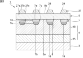
- FIG. 3 is a front sectional view showing the vicinity of two pairs of electrode fingers of the first IDT electrode and the second IDT electrode in the acoustic wave device according to the first embodiment of the present invention.
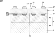
- FIG. 4 is a front sectional view showing the vicinity of two pairs of electrode fingers of a first IDT electrode and a second IDT electrode in an acoustic wave device according to a second embodiment of the present invention.
- FIG. 1 is a front sectional view of an elastic wave device according to a first embodiment of the present invention.
- FIG. 2 is a bottom view showing the electrode structure on the first main surface of the piezoelectric layer in the first embodiment of the present invention.
- FIG. 3 is a front sectional view showing the vicinity of two pairs of electrode fingers of the
- FIG. 5 is a front sectional view showing the vicinity of two pairs of electrode fingers of a first IDT electrode and a second IDT electrode in an acoustic wave device according to a third embodiment of the present invention.
- FIG. 6 is a front sectional view showing the vicinity of two pairs of electrode fingers of the first IDT electrode and the second IDT electrode in an acoustic wave device according to the fourth embodiment of the present invention.
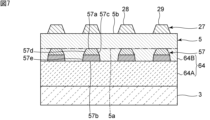
- FIG. 7 is a front sectional view showing the vicinity of two pairs of electrode fingers of the first IDT electrode and the second IDT electrode in an acoustic wave device according to a modification of the fourth embodiment of the present invention.
- FIG. 8 is a schematic plan view of an elastic wave device according to a fifth embodiment of the present invention.
- FIG. 9 is a diagram showing impedance frequency characteristics in the first embodiment and the fifth embodiment of the present invention.
- FIG. 10 is a schematic plan view of an elastic wave device according to a sixth embodiment of the present invention.
- FIG. 11 is a front sectional view showing the vicinity of two pairs of electrode fingers of a first IDT electrode and a second IDT electrode in an acoustic wave device according to a seventh embodiment of the present invention.
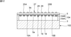
- FIG. 12 is a front sectional view of an elastic wave device according to a modification of the seventh embodiment of the present invention.
- FIG. 1 is a front sectional view of an elastic wave device according to a first embodiment of the present invention.
- the elastic wave device 1 has a piezoelectric substrate 2.
- the piezoelectric substrate 2 has a support substrate 3, an intermediate layer 4, and a piezoelectric layer 5.
- the intermediate layer 4 is a laminate. More specifically, the intermediate layer 4 has a first layer 4A and a second layer 4B. A first layer 4A of the intermediate layer 4 is provided on the support substrate 3. A second layer 4B is provided on the first layer 4A. A piezoelectric layer 5 is provided on the second layer 4B. Note that the intermediate layer 4 may be a single dielectric layer or the like.
- the piezoelectric layer 5 has a first main surface 5a and a second main surface 5b.
- the first main surface 5a and the second main surface 5b are opposed to each other.
- the first main surface 5a is located on the intermediate layer 4 side.
- a first IDT electrode 7 is provided on the first main surface 5a of the piezoelectric layer 5.
- the first IDT electrode 7 is embedded in the intermediate layer 4 .
- a second IDT electrode 27 is provided on the second main surface 5b of the piezoelectric layer 5.
- FIG. 2 is a bottom view showing the electrode structure on the first main surface of the piezoelectric layer in the first embodiment. Note that FIG. 1 is a cross-sectional view taken along line II in FIG. 2.
- the first IDT electrode 7 has a pair of bus bars, a plurality of first electrode fingers 18 and a plurality of second electrode fingers 19.
- the pair of busbars is a first busbar 16 and a second busbar 17.
- the first bus bar 16 and the second bus bar 17 are opposed to each other.
- One end of a plurality of first electrode fingers 18 is connected to the first bus bar 16, respectively.
- One end of a plurality of second electrode fingers 19 is connected to the second bus bar 17, respectively.
- the plurality of first electrode fingers 18 and the plurality of second electrode fingers 19 are inserted into each other.
- the first electrode finger 18 and the second electrode finger 19 are connected to different potentials.
- the second IDT electrode 27 shown in FIG. 1 also has a pair of bus bars, a plurality of third electrode fingers 28, and a plurality of fourth electrode fingers 29.
- the pair of bus bars of the second IDT electrode 27 is a third bus bar and a fourth bus bar.
- the third bus bar and the fourth bus bar face each other.
- One end of the plurality of third electrode fingers 28 is each connected to the third bus bar.
- One end of the plurality of fourth electrode fingers 29 is each connected to the fourth bus bar.
- the plurality of third electrode fingers 28 and the plurality of fourth electrode fingers 29 are inserted into each other.
- the third electrode finger 28 and the fourth electrode finger 29 are connected to different potentials.
- the first electrode finger 18, the second electrode finger 19, the third electrode finger 28, and the fourth electrode finger 29 may be simply referred to as electrode fingers.
- the direction in which a plurality of electrode fingers extend is defined as an electrode finger extension direction.
- the extending directions of the electrode fingers of the first IDT electrode 7 and the second IDT electrode 27 are parallel.
- a pair of reflectors 15A and 15B are provided on the first main surface 5a of the piezoelectric layer 5.
- the reflector 15A and the reflector 15B face each other with the first IDT electrode 7 in between in a direction perpendicular to the direction in which the electrode fingers extend.
- a pair of reflectors 25A and 25B are provided on the second main surface 5b.
- the reflector 25A and the reflector 25B face each other with the second IDT electrode 27 in between in a direction perpendicular to the electrode finger extending direction.
- the first IDT electrode 7, reflector 15A, and reflector 15B are formed by laminating a Pt layer and an Al layer in this order from the piezoelectric layer 5 side.
- the second IDT electrode 27, reflector 25A, and reflector 25B are made of an Al layer.
- the materials and number of layers of the first IDT electrode 7, the second IDT electrode 27, and each reflector are not limited to the above.
- the first IDT electrode 7, the reflector 15A, and the reflector 15B may be made of, for example, a laminated metal film of three or more layers, or may be made of a single-layer metal film.
- the second IDT electrode 27, reflector 25A, and reflector 25B may be made of a laminated metal film.
- FIG. 3 is a front sectional view showing the vicinity of two pairs of electrode fingers of the first IDT electrode and the second IDT electrode in the acoustic wave device according to the first embodiment.
- Each electrode finger of the first IDT electrode 7 includes a first surface 7a, a second surface 7b, and a side surface 7c.
- the first surface 7a and the second surface 7b face each other in the thickness direction of each electrode finger.
- the first surface 7a is located on the piezoelectric layer 5 side.
- the side surface 7c is a surface connecting the first surface 7a and the second surface 7b.
- the side surface 7c of each electrode finger has a first portion 7d and a second portion 7e. More specifically, the first portion 7d and the second portion 7e are lined up in the thickness direction of each electrode finger. Of the first portion 7d and the second portion 7e, the first portion 7d is located on the piezoelectric layer 5 side.
- the end of the first portion 7d on the support substrate 3 side is connected to the end of the second portion 7e on the piezoelectric layer 5 side.
- the first portion 7d of the side surface 7c is a side surface of the Pt layer
- the second portion 7e is a side surface of the Al layer.
- the angle ⁇ at which the side surface 7c of the electrode finger is inclined with respect to the thickness direction of the electrode finger is defined as the inclination angle.
- the inclination angle is assumed to be a positive value.
- the angle of inclination is assumed to be a negative value.
- the width of the electrode finger is the dimension of the electrode finger along the direction perpendicular to the extending direction of the electrode finger. In the first IDT electrode 7 of the acoustic wave device 1, the side surface 7c of each electrode finger is inclined such that the width of the electrode finger becomes narrower as the distance from the piezoelectric layer 5 increases.
- the feature of this embodiment is that in the first IDT electrode 7 embedded in the intermediate layer 4, the side surface 7c of each electrode finger has a first portion 7d and a second portion 7e, and the first portion The reason is that the inclination angles of the second portion 7d and the second portion 7e are different from each other.
- the inclination angles of the first portion 7d and the second portion 7e may be different from each other.
- the first IDT electrode 7 can be formed, for example, by a lift-off method using a vacuum evaporation method, a sputtering method, or the like. At this time, by making the film forming speed for forming the portion including the first portion 7d of each electrode finger different from the film forming speed for forming the portion including the second portion 7e, The first portion 7d and the second portion 7e can have different inclination angles.
- the method for forming the first IDT electrode 7 is not limited to the above.
- the inclination angles of the first portion 7d and the second portion 7e may be made different from each other by etching or the like.
- the area where adjacent electrode fingers overlap when viewed from a direction perpendicular to the direction in which the electrode fingers extend is an intersection area C.
- the second IDT electrode 27 also has an intersection region.
- planar view refers to viewing from a direction corresponding to the upper side in FIG.
- the piezoelectric layer 5 is located above.
- the centers of the plurality of electrode fingers in the intersection region C of the first IDT electrode 7 and the centers of the plurality of electrode fingers in the intersection region of the second IDT electrode 27 overlap in plan view.
- the two intersection regions overlap in plan view within an error range that does not significantly affect the electrical characteristics of the acoustic wave device. Therefore, the deviation due to manufacturing variations is included in the fact that both intersecting regions overlap in plan view.
- the electrode finger pitch of the first IDT electrode 7 and the second IDT electrode 27 is the same. Note that the electrode finger pitch is the distance between the centers of adjacent electrode fingers. In this specification, the term “the electrode finger pitches are the same” also includes the electrode finger pitches being different within an error range that does not significantly affect the electrical characteristics of the acoustic wave device.
- the third electrode finger 28 of the second IDT electrode 27 shown in FIG. connected to.
- the fourth electrode finger 29 is connected to the same potential as the other of the first electrode finger 18 and the second electrode finger 19.
- the potentials of the overlapping electrode fingers in plan view are in phase.
- the relationship between the potentials of the electrode fingers of the first IDT electrode 7 and the electrode fingers of the second IDT electrode 27 is not limited to the above.
- the potentials of at least one pair of electrode fingers among a plurality of pairs of electrode fingers overlapping in plan view may be in phase.
- each reflector 15A, the reflector 15B, the reflector 25A, and the reflector 25B may be the same potential as the first electrode finger 18 of the first IDT electrode 7, and the same potential as the second electrode finger 19. It may be.
- each reflector may be a floating electrode.
- a floating electrode is an electrode that is not connected to a signal potential or a ground potential.
- silicon is used as the material for the support substrate 3.
- the material of the support substrate 3 is not limited to the above, and includes, for example, aluminum nitride, lithium tantalate, lithium niobate, piezoelectric materials such as crystal, alumina, sapphire, magnesia, silicon nitride, silicon carbide, zirconia, cordierite, Ceramics such as mullite, steatite, and forsterite, dielectrics such as diamond and glass, semiconductors such as silicon and gallium nitride, resins, or materials containing the above-mentioned materials as main components can be used.
- main component refers to a component that accounts for more than 50 wt% in a member.
- the above-mentioned main component material may exist in any one of single crystal, polycrystal, and amorphous state, or in a mixed state of these.
- Silicon nitride is used as the material for the first layer 4A of the intermediate layer 4.
- the material of the first layer 4A is not limited to the above, and includes, for example, aluminum nitride, lithium tantalate, lithium niobate, piezoelectric material such as crystal, alumina, sapphire, magnesia, silicon nitride, silicon carbide, zirconia, and Ceramics such as light, mullite, steatite, forsterite, spinel, and sialon; dielectrics such as aluminum oxide, silicon oxynitride, DLC (diamond-like carbon), and diamond; semiconductors such as silicon; Materials that can be used can be used.
- the spinel includes an aluminum compound containing oxygen and one or more elements selected from Mg, Fe, Zn, Mn, etc.
- the spinel include MgAl 2 O 4 , FeAl 2 O 4 , ZnAl 2 O 4 and MnAl 2 O 4 .
- Silicon oxide is used as the material for the second layer 4B of the intermediate layer 4.
- the material of the second layer 4B is not limited to the above, and for example, a dielectric material such as glass, silicon oxide, silicon oxynitride, lithium oxide, tantalum oxide, or a compound obtained by adding fluorine, carbon, or boron to silicon oxide. , or a material whose main component is the above-mentioned material can be used.
- the example of the material of the first layer 4A of the intermediate layer 4 is different from the example of the material of the second layer 4B.
- the materials listed as examples of the materials for the first layer 4A may be used for the second layer 4B.
- the materials listed as examples of the materials for the second layer 4B may be used for the first layer 4A.
- the number of layers of the intermediate layer 4 is not particularly limited, and may be one layer or three or more layers. When the intermediate layer 4 has a plurality of layers, the materials of the plurality of layers may be different from each other.
- Lithium niobate is used as the material for the piezoelectric layer 5.
- the material of the piezoelectric layer 5 is not limited to the above, and for example, lithium tantalate, zinc oxide, aluminum nitride, crystal, PZT (lead zirconate titanate), etc. can also be used.
- the expression that the first IDT electrode 7 is embedded in the intermediate layer 4 means that the side surfaces 7c of the plurality of electrode fingers of the first IDT electrode 7 are in contact with the intermediate layer 4.
- the first IDT electrode 7 is embedded in the intermediate layer 4 even when the second surfaces 7b of the plurality of electrode fingers are in contact with a member other than the intermediate layer 4.
- the portion of the intermediate layer 4 where the first IDT electrode 7 is embedded is the second layer 4B.
- the material of the second layer 4B and the material of the piezoelectric layer 5 are different from each other. Note that the material of the portion of the intermediate layer 4 where the first IDT electrode 7 is embedded may be the same as the material of the piezoelectric layer 5.
- the first IDT electrode 7 is directly provided on the first main surface 5a of the piezoelectric layer 5.
- the first IDT electrode 7 may be provided indirectly on the first main surface 5a via a dielectric film.
- each electrode finger of the second IDT electrode 27 includes a third surface 27a, a fourth surface 27b, and a side surface 27c.
- the third surface 27a and the fourth surface 27b face each other in the thickness direction of each electrode finger.
- the third surface 27a is located on the piezoelectric layer 5 side.
- a side surface 27c is connected to the third surface 27a and the fourth surface 27b.
- the side surface 27c of each electrode finger is inclined with respect to the thickness direction of each electrode finger. More specifically, the side surface 27c of each electrode finger is inclined such that the width of each electrode finger becomes narrower as the distance from the piezoelectric layer 5 increases. Note that the side surface 27c of each electrode finger may extend parallel to the thickness direction of each electrode finger.
- the inclination angles of the first portion 7d and the second portion 7e may be different from each other.
- the inclination angles of the first portion 7d and the second portion 7e of the plurality of electrode fingers are different from each other. More preferably, the inclination angles of the first portion 7d and the second portion 7e are different from each other in all electrode fingers.
- the inclination angles at the first portion 7d and the second portion 7e of each electrode finger are not 0°.
- the inclination angle of one of the first portion 7d and the second portion 7e may be 0°.
- the inclination angle of the second portion 7e is larger than the inclination angle of the first portion 7d. Note that the angle of inclination of the second portion 7e may be smaller than the angle of inclination of the first portion 7d.
- the side surface 7c of each electrode finger of the first IDT electrode 7 in the elastic wave device 1 has a first portion 7d and a second portion 7e as a plurality of portions.
- the plurality of portions on the side surface 7c is not limited to two portions, and may be three or more portions.
- three or more portions may be lined up in the thickness direction of the electrode finger, and the ends of adjacent portions may be connected to each other.
- FIG. 4 is a front sectional view showing the vicinity of two pairs of electrode fingers of the first IDT electrode and the second IDT electrode in the acoustic wave device according to the second embodiment.
- the side surface 37c of each electrode finger of the first IDT electrode 37 has a first portion 37d, a second portion 37e, and a third portion 37f as a plurality of portions. Different from the embodiment. The first portion 37d, the second portion 37e, and the third portion 37f are arranged in this order in the thickness direction of the electrode finger.
- the elastic wave device of this embodiment has the same configuration as the elastic wave device 1 of the first embodiment.
- the inclination angle of the second portion 37e of each electrode finger of the first IDT electrode 37 is the largest among the inclination angles of the plurality of portions.
- the inclination angle of the first portion 37d is the smallest among the inclination angles of the plurality of portions. Therefore, the inclination angle of the third portion 37f is greater than the inclination angle of the first portion 37d and smaller than the inclination angle of the second portion 37e.
- the side surface 37c of each electrode finger has a plurality of portions having different inclination angles. Thereby, the bonding force between the first IDT electrode 37 and the intermediate layer 4 can be effectively increased. Therefore, peeling between the first IDT electrode 37 and the intermediate layer 4 can be effectively suppressed.
- the magnitude relationship of the inclination angles of the plurality of portions of the side surface 37c is not limited to the above.
- the inclination angle may be increased, or the inclination angle may be decreased in the above order.
- FIG. 5 is a front sectional view showing the vicinity of two pairs of electrode fingers of the first IDT electrode and the second IDT electrode in the acoustic wave device according to the third embodiment.
- This embodiment differs from the first embodiment in that a dielectric film 46 is provided between the piezoelectric layer 5 and the first IDT electrode 7. More specifically, the dielectric film 46 is directly provided on the first main surface 5a of the piezoelectric layer 5. The first IDT electrode 7 is indirectly provided on the first main surface 5a of the piezoelectric layer 5 with a dielectric film 46 interposed therebetween. Note that the dashed line in FIG. 5 indicates the boundary between the dielectric film 46 and the intermediate layer 4. Other than the above points, the elastic wave device of this embodiment has the same configuration as the elastic wave device 1 of the first embodiment.
- Silicon oxide is used as the material for the dielectric film 46.
- the material of the dielectric film 46 is not limited to the above, and a dielectric such as silicon nitride may also be used.
- the dielectric film 46 and the second layer 4B of the intermediate layer 4 are integrally formed of the same material. Note that the dielectric film 46 and the second layer 4B of the intermediate layer 4 may be made of different materials.
- the fractional band and element capacitance of the acoustic wave device can be easily adjusted.
- the first IDT electrode 7 is embedded in the intermediate layer 4, and the first portion 7d and the second portion of the side surface 7c of each electrode finger in the first IDT electrode 7 are embedded in the intermediate layer 4.
- the inclination angles of the portions 7e are different from each other. Thereby, the bonding force between the first IDT electrode 7 and the intermediate layer 4 can be increased. Therefore, separation between the first IDT electrode 7 and the intermediate layer 4 is unlikely to occur.
- FIG. 6 is a front sectional view showing the vicinity of two pairs of electrode fingers of the first IDT electrode and the second IDT electrode in the acoustic wave device according to the fourth embodiment.
- This embodiment differs from the first embodiment in the configuration of the intermediate layer 54. This embodiment also differs from the first embodiment in the configuration of the side surface 57c of each electrode finger of the first IDT electrode 57. Other than the above points, the elastic wave device of this embodiment has the same configuration as the elastic wave device 1 of the first embodiment.
- the intermediate layer 54 is a single layer and made of a piezoelectric material. More specifically, the material of the intermediate layer 54 and the material of the piezoelectric layer 5 are the same.
- the dashed line in FIG. 6 indicates the boundary between the intermediate layer 54 and the piezoelectric layer 5.
- the first main surface 5a of the piezoelectric layer 5 is a surface through which the first surfaces 57a of the plurality of electrode fingers in the first IDT electrode 57 pass.
- the piezoelectric layer 5 and the intermediate layer 54 are integrally made of the same material. Therefore, in the acoustic wave device of this embodiment, the first IDT electrode 57 is embedded in the piezoelectric layer. Note that the piezoelectric layer in which the first IDT electrode 57 is embedded is a piezoelectric layer in which the piezoelectric layer 5 and the intermediate layer 54 shown in FIG. 6 are integrated. This piezoelectric layer is provided directly on the support substrate 3.
- each electrode finger of the first IDT electrode 57 is inclined such that the width of the electrode finger becomes wider as the distance from the piezoelectric layer 5 increases.
- the inclination angles of the first portion 57d and the second portion 57e are negative values.
- the angle of inclination of the second portion 57e is greater than the angle of inclination of the first portion 57d. Note that the absolute value of the inclination angle of the second portion 57e is smaller than the absolute value of the inclination angle of the first portion 57d.
- the first IDT electrode 57 is embedded in the intermediate layer 54, and the first portion 57d of the side surface 57c of each electrode finger in the first IDT electrode 57
- the inclination angles of the second portion 57e and the second portion 57e are different from each other. Therefore, the bonding force between the first IDT electrode 57 and the intermediate layer 54 can be increased. Therefore, separation between the first IDT electrode 57 and the intermediate layer 54 is unlikely to occur.
- the second surface 57b of the plurality of electrode fingers in the first IDT electrode 57 is in contact with the support substrate 3.
- the first IDT electrode 57 may be formed on the support substrate 3, for example.
- a piezoelectric layer may be formed on the support substrate 3 so as to cover the first IDT electrode 57.
- the piezoelectric layer can be formed by, for example, a sputtering method. Note that this piezoelectric layer is a piezoelectric layer in which the intermediate layer 54 and the piezoelectric layer 5 shown in FIG. 6 are integrally formed.
- the method of forming the first IDT electrode 57 and the piezoelectric layer is not limited to the above method.
- grooves may be provided in the piezoelectric layer.
- the first IDT electrode 57 may be formed within this groove.
- the intermediate layer 64 has multiple layers. More specifically, the intermediate layer 64 includes a first layer 64A and a second layer 64B.
- the first IDT electrode 57 is not embedded in the first layer 64A.
- the second layer 64B is a portion of the intermediate layer 64 in which the first IDT electrode 57 is embedded.
- the material of the second layer 64B and the material of the piezoelectric layer 5 are the same.
- the material of the first layer 64A and the material of the piezoelectric layer 5 are different.
- the second surface 57b of each electrode finger of the first IDT electrode 57 is in contact with the first layer 64A.
- the second layer 64B of the intermediate layer 64 and the piezoelectric layer 5 are integrally configured.
- This integrated piezoelectric layer is provided indirectly on the support substrate 3 via the first layer 64A of the intermediate layer 64. Also in this modification, peeling is unlikely to occur between the first IDT electrode 57 and the intermediate layer 64, as in the fourth embodiment.
- FIG. 8 is a schematic plan view of the elastic wave device according to the fifth embodiment.
- the reflector is omitted. Note that since FIG. 8 is a schematic plan view, compared to FIG. 2 which is a bottom view, FIG. 8 has an arrangement in which not only the front and back are reversed, but also the top and bottom are reversed.
- This embodiment differs from the first embodiment in that a first wiring 72 and a second wiring 73 are provided.
- the elastic wave device of this embodiment has the same configuration as the elastic wave device 1 of the first embodiment.
- the plurality of fourth electrode fingers 29 of the second IDT electrode 27 are connected to a potential in opposite phase to the plurality of first electrode fingers 18 of the first IDT electrode 7.
- the first wiring 72 is provided on the first main surface 5a of the piezoelectric layer 5.
- the first wiring 72 is connected to the first bus bar 16 of the first IDT electrode 7 .
- the first wiring 72 is electrically connected to the plurality of first electrode fingers 18 via the first bus bar 16 .
- the first wiring 72 and the first bus bar 16 are integrally formed of the same material.
- the first wiring 72 and the first bus bar 16 may be made of different materials.
- the second wiring 73 is provided on the second main surface 5b of the piezoelectric layer 5.
- the second wiring 73 is connected to the fourth bus bar 77 of the second IDT electrode 27.
- the second wiring 73 is electrically connected to the plurality of fourth electrode fingers 29 via a fourth bus bar 77 .
- the second wiring 73 and the fourth bus bar 77 are integrally formed of the same material.
- the second wiring 73 and the fourth bus bar 77 may be made of different materials.
- the plurality of first electrode fingers 18 and the plurality of fourth electrode fingers 29 are connected to potentials in opposite phases to each other. Therefore, for example, when the first wiring 72, the first bus bar 16, and the plurality of first electrode fingers 18 are at a negative potential, the second wiring 73, the fourth bus bar 77, and the plurality of fourth electrodes Finger 29 has a positive potential.
- a part of the first wiring 72 and a part of the second wiring 73 overlap in plan view.
- the overlapping region D is configured. More specifically, in the overlapping region D, the first wiring 72 and the second wiring 73 face each other with the piezoelectric layer 5 in between. Thereby, the element capacitance can be increased. This effect will be shown below by comparing this embodiment and the first embodiment.
- FIG. 9 is a diagram showing impedance frequency characteristics in the first embodiment and the fifth embodiment.
- the impedance in the fifth embodiment is lower than the impedance in the first embodiment. Therefore, it can be seen that in the fifth embodiment, the element capacitance can be increased. Thereby, in the fifth embodiment, the areas of the first IDT electrode 7 and the second IDT electrode 27 can be reduced in order to obtain the desired element capacitance. Therefore, in the fifth embodiment, the elastic wave device can be made smaller.
- /fr) ⁇ 100[%] is the fractional band of the elastic wave device.
- the difference between the resonant frequency fr and the anti-resonant frequency fa is different between the fifth embodiment and the first embodiment. Therefore, the fractional bands are different between the fifth embodiment and the first embodiment. This is because the fractional band depends on the element capacitance. Note that in the fifth embodiment, by adjusting the area of the overlapping region D, the element capacitance can be easily adjusted. Thereby, the fractional band can be easily adjusted.
- the first IDT electrode 7 is embedded in the intermediate layer, and the first IDT electrode 7 on the side surface of each electrode finger in the first IDT electrode 7 is similar to the first embodiment.
- the inclination angles of the portion and the second portion are different from each other. Therefore, the bonding force between the first IDT electrode 7 and the intermediate layer can be increased. Therefore, peeling is unlikely to occur between the first IDT electrode 7 and the intermediate layer.
- FIG. 8 schematically shows the arrangement of the first wiring 72 and the second wiring 73, and the reflector is omitted.
- the overlapping region D may be located outside the reflector in the elastic wave propagation direction.
- a reflector may be located between the overlapping region D and the first IDT electrode 7.
- one first wiring 72 and one second wiring 73 are provided.
- two each of the first wiring 72 and the second wiring 73 may be provided.
- FIG. 10 is a schematic plan view of an elastic wave device according to the sixth embodiment.
- This embodiment differs from the fifth embodiment in that two first wirings and two second wirings are provided. Specifically, the two first wirings are a first wiring 82A and a first wiring 82B. Specifically, the two second wirings are a second wiring 83A and a second wiring 83B. This embodiment also differs from the fifth embodiment in that the first wiring 82A and the first wiring 82B and the second wiring 83A and the second wiring 83B are each reflectors. Other than the above points, the elastic wave device of this embodiment has the same configuration as the elastic wave device of the fifth embodiment.
- the first wiring 82A and the first wiring 82B are provided on the first main surface 5a of the piezoelectric layer 5, similarly to the fifth embodiment.
- the first wiring 82A has a reflector section 82c and a wiring section 82d.
- the reflector portion 82c is a portion that functions as a reflector.
- a wiring section 82d is connected to the reflector section 82c.
- the wiring portion 82d is connected to the first bus bar 16 of the first IDT electrode 7.
- the first wiring 82B has a reflector portion 82e and a wiring portion 82f.
- the wiring section 82f connects the reflector section 82e and the first bus bar 16.
- the reflector portion 82c and the reflector portion 82e face each other with the first IDT electrode 7 in between.
- the second wiring 83A and the second wiring 83B are provided on the second main surface 5b of the piezoelectric layer 5.
- the second wiring 83A includes a reflector section 83c and a wiring section 83d.
- the wiring section 83d connects the reflector section 83c and the fourth bus bar 77.
- the second wiring 83B has a reflector portion 83e and a wiring portion 83f.
- the wiring section 83f connects the reflector section 83e and the fourth bus bar 77.
- the reflector portion 83c and the reflector portion 83e face each other with the second IDT electrode 27 in between.
- the plurality of first electrode fingers 18 and the plurality of fourth electrode fingers 29 are connected to potentials in opposite phases to each other. Therefore, for example, when the first wiring 82A, the first wiring 82B, the first bus bar 16, and the plurality of first electrode fingers 18 are at a negative potential, the second wiring 83A, the second wiring 83B, and the fourth bus bar 77 and the plurality of fourth electrode fingers 29 are at a positive potential.
- the reflector portion 82c of the first wiring 82A and the reflector portion 83c of the second wiring 83A overlap in plan view. More specifically, the reflector portion 82c and the reflector portion 83c face each other with the piezoelectric layer 5 in between. Similarly, the reflector portion 82e of the first wiring 82B and the reflector portion 83e of the second wiring 83B overlap in plan view. More specifically, the reflector portion 82e and the reflector portion 83e face each other with the piezoelectric layer 5 in between. Thereby, the element capacitance can be increased.
- the first IDT electrode 7 is embedded in the intermediate layer, and each electrode finger in the first IDT electrode 7 is The first portion and the second portion of the side surface have different inclination angles. Thereby, the bonding force between the first IDT electrode 7 and the intermediate layer can be increased. Therefore, peeling is unlikely to occur between the first IDT electrode 7 and the intermediate layer.
- both the first wiring 82A and the second wiring 83A are reflectors. Both the first wiring 82B and the second wiring 83B are reflectors. However, it is sufficient if at least one of the first wiring 82A and the second wiring 83A is a reflector. Similarly, at least one of the first wiring 82B and the second wiring 83B may be a reflector.
- the acoustic wave device may include a protective film such as a silicon oxide film or a silicon nitride film that covers the second IDT electrode.
- FIG. 11 is a front sectional view showing the vicinity of two pairs of electrode fingers of the first IDT electrode and the second IDT electrode in the elastic wave device according to the seventh embodiment.
- This embodiment differs from the first embodiment in that the thickness of the second layer 94B in the intermediate layer 94 is thinner than the thickness of each electrode finger of the first IDT electrode 7. This embodiment also differs from the first embodiment in that a part of the first layer 94A in the intermediate layer 94 is located between the electrode fingers of the first IDT electrode 7. Other than the above points, the elastic wave device of this embodiment has the same configuration as the elastic wave device 1 of the first embodiment.
- the portion of the intermediate layer 94 in which the first IDT electrode 7 is embedded is a portion of the intermediate layer 94 that covers the first IDT electrode 7 . That is, in this embodiment, the first IDT electrode 7 is embedded in the second layer 94B of the intermediate layer 94.
- the inclination angles of the first portion 7d and the second portion 7e of the side surface 7c of each electrode finger in the first IDT electrode 7 are different from each other. Thereby, the bonding force between the first IDT electrode 7 and the intermediate layer 94 can be increased. Therefore, separation between the first IDT electrode 7 and the intermediate layer 94 is unlikely to occur.
- the support substrate 3 may face the first IDT electrode 7 embedded in the intermediate layer 94 with a cavity in between.
- the first layer 104A of the intermediate layer 104 has a frame-like shape.
- the second layer 104B of the intermediate layer 104 covers the first IDT electrode 7 similarly to the seventh embodiment. That is, the first IDT electrode 7 is embedded in the second layer 104B of the intermediate layer 104.
- a cavity surrounded by the first layer 104A, the second layer 104B, and the support substrate 3 in the intermediate layer 104 is configured. Therefore, the piezoelectric substrate 102 has a cavity.
- the support substrate 3 faces the first IDT electrode 7 embedded in the second layer 104B of the intermediate layer 104 across the cavity. Also in this modification, as in the seventh embodiment, peeling is unlikely to occur between the first IDT electrode 7 and the second layer 104B of the intermediate layer 104.
- the materials of the first layer 104A and the second layer 104B in the intermediate layer 104 are different from each other.
- the first layer 104A and the second layer 104B may be made of the same material.
- the configuration in which the second layer of the intermediate layer has a frame-like shape and the piezoelectric substrate has a cavity can also be adopted in configurations of the present invention other than this modification.
- the first layer 4A of the intermediate layer 4 in the first embodiment shown in FIG. 1 may have a frame-like shape.
- the first layer 64A of the intermediate layer 64 in the modification of the fourth embodiment shown in FIG. 7 may have a frame-like shape. Even in these cases, peeling is unlikely to occur between the first IDT electrode and the second layer of the intermediate layer.
- a support substrate an intermediate layer provided on the support substrate, a first main surface provided on the intermediate layer and located on the intermediate layer side, and a first main surface provided on the intermediate layer and located on the intermediate layer side; a piezoelectric layer having a second main surface facing the main surface; a first IDT electrode provided on the first main surface of the piezoelectric layer and embedded in the intermediate layer; , a second IDT electrode provided on the second main surface of the piezoelectric layer, wherein the first IDT electrode has a plurality of electrode fingers, and each electrode finger is connected to the second main surface of the piezoelectric layer.
- the first IDT electrode includes a first surface and a second surface facing each other in the thickness direction of the electrode finger, and a side surface connected to the first surface and the second surface.
- the side surface of the electrode finger has a first part and a second part, and in at least one of the electrode fingers, the first part and the second part have a thickness direction of the electrode finger.
- An elastic wave device that has different angles of inclination relative to each other.
- ⁇ 3> The acoustic wave device according to ⁇ 1> or ⁇ 2>, wherein a material of a portion of the intermediate layer where the first IDT electrode is embedded is different from a material of the piezoelectric layer.
- ⁇ 4> The acoustic wave device according to ⁇ 3>, wherein the first IDT electrode is directly provided on the first main surface of the piezoelectric layer.
- ⁇ 5> Further comprising a dielectric film provided directly on the first main surface of the piezoelectric layer, the first IDT electrode on the first main surface of the piezoelectric layer, The acoustic wave device according to ⁇ 3>, which is indirectly provided via the dielectric film.
- ⁇ 6> The acoustic wave device according to ⁇ 1> or ⁇ 2>, wherein the material of the portion of the intermediate layer where the first IDT electrode is embedded is the same as the material of the piezoelectric layer.
- ⁇ 7> The elastic wave device according to any one of ⁇ 1> to ⁇ 6>, wherein the intermediate layer has a plurality of layers made of different materials.
- the plurality of electrode fingers of the first IDT electrode include a plurality of first electrode fingers and a plurality of second electrode fingers connected to mutually different potentials, and the second IDT electrode
- the electrode includes a plurality of third electrode fingers and a plurality of fourth electrode fingers connected to mutually different potentials, and the plurality of fourth electrode fingers are connected to the plurality of first electrode fingers.
- a first wiring connected to an opposite phase potential and electrically connected to the plurality of first electrode fingers of the first IDT electrode; and the plurality of fourth electrode fingers of the second IDT electrode.
Landscapes
- Physics & Mathematics (AREA)
- Acoustics & Sound (AREA)
- Chemical & Material Sciences (AREA)
- Engineering & Computer Science (AREA)
- Materials Engineering (AREA)
- Surface Acoustic Wave Elements And Circuit Networks Thereof (AREA)
Abstract
Description
2…圧電性基板
3…支持基板
4…中間層
4A,4B…第1,第2の層
5…圧電体層
5a,5b…第1,第2の主面
7…第1のIDT電極
7a,7b…第1,第2の面
7c…側面
7d,7e…第1,第2の部分
15A,15B…反射器
16,17…第1,第2のバスバー
18,19…第1,第2の電極指
25A,25B…反射器
27…第2のIDT電極
27a,27b…第3,第4の面
27c…側面
28,29…第3,第4の電極指
37…第1のIDT電極
37c…側面
37d~37f…第1~第3の部分
46…誘電体膜
54…中間層
57…第1のIDT電極
57a,57b…第1,第2の面
57c…側面
57d,57e…第1,第2の部分
64…中間層
64A,64B…第1,第2の層
72,73…第1,第2配線
77…第4のバスバー
82A,82B…第1配線
82c…反射器部
82d…配線部
82e…反射器部
82f…配線部
83A,83B…第2配線
83c…反射器部
83d…配線部
83e…反射器部
83f…配線部
94…中間層
94A,94B…第1,第2の層
102…圧電性基板
104…中間層
104A,104B…第1,第2の層
C…交叉領域
D…重なり領域
Claims (9)
- 支持基板と、
前記支持基板上に設けられている中間層と、
前記中間層上に設けられており、前記中間層側に位置している第1の主面、及び前記第1の主面と対向している第2の主面を有する圧電体層と、
前記圧電体層の前記第1の主面に設けられており、前記中間層に埋め込まれている第1のIDT電極と、
前記圧電体層の前記第2の主面に設けられている第2のIDT電極と、
を備え、
前記第1のIDT電極が複数の電極指を有し、各前記電極指がそれぞれ、前記電極指の厚み方向において互いに対向している第1の面及び第2の面と、前記第1の面及び前記第2の面に接続されている側面と、を含み、
前記第1のIDT電極における前記電極指の前記側面が、第1の部分及び第2の部分を有し、少なくとも1本の前記電極指において、前記第1の部分及び前記第2の部分の、前記電極指の厚み方向に対して傾斜している角度が互いに異なる、弾性波装置。 - 前記第1のIDT電極における全ての前記電極指の前記側面において、前記第1の部分及び前記第2の部分の、前記電極指の厚み方向に対して傾斜している角度が互いに異なる、請求項1に記載の弾性波装置。
- 前記中間層における前記第1のIDT電極が埋め込まれている部分の材料と、前記圧電体層の材料とが互いに異なる、請求項1または2に記載の弾性波装置。
- 前記圧電体層の前記第1の主面に、前記第1のIDT電極が直接的に設けられている、請求項3に記載の弾性波装置。
- 前記圧電体層の前記第1の主面に直接的に設けられている誘電体膜をさらに備え、
前記圧電体層の前記第1の主面に、前記第1のIDT電極が、前記誘電体膜を介して間接的に設けられている、請求項3に記載の弾性波装置。 - 前記中間層における前記第1のIDT電極が埋め込まれている部分の材料と、前記圧電体層の材料とが同じである、請求項1または2に記載の弾性波装置。
- 前記中間層が、材料が互いに異なる複数の層を有する、請求項1~6のいずれか1項に記載の弾性波装置。
- 前記第1のIDT電極の前記複数の電極指が、互いに異なる電位に接続される複数の第1の電極指と、複数の第2の電極指と、を含み、
前記第2のIDT電極が、互いに異なる電位に接続される複数の第3の電極指と、複数の第4の電極指と、を含み、前記複数の第4の電極指が、前記複数の第1の電極指と逆相の電位に接続され、
前記第1のIDT電極の前記複数の第1の電極指に電気的に接続された第1配線と、
前記第2のIDT電極の前記複数の第4の電極指に電気的に接続された第2配線と、
をさらに備え、
前記第1配線の一部と前記第2配線の一部とは、平面視において重なっている、請求項1~7のいずれか1項に記載の弾性波装置。 - 前記第1配線及び前記第2配線のうち少なくとも一方は、反射器である、請求項8に記載の弾性波装置。
Priority Applications (2)
| Application Number | Priority Date | Filing Date | Title |
|---|---|---|---|
| CN202380052132.6A CN119422327A (zh) | 2022-07-15 | 2023-06-01 | 弹性波装置 |
| US19/013,252 US20250150057A1 (en) | 2022-07-15 | 2025-01-08 | Acoustic wave device |
Applications Claiming Priority (2)
| Application Number | Priority Date | Filing Date | Title |
|---|---|---|---|
| JP2022-113606 | 2022-07-15 | ||
| JP2022113606 | 2022-07-15 |
Related Child Applications (1)
| Application Number | Title | Priority Date | Filing Date |
|---|---|---|---|
| US19/013,252 Continuation US20250150057A1 (en) | 2022-07-15 | 2025-01-08 | Acoustic wave device |
Publications (1)
| Publication Number | Publication Date |
|---|---|
| WO2024014167A1 true WO2024014167A1 (ja) | 2024-01-18 |
Family
ID=89536613
Family Applications (1)
| Application Number | Title | Priority Date | Filing Date |
|---|---|---|---|
| PCT/JP2023/020538 Ceased WO2024014167A1 (ja) | 2022-07-15 | 2023-06-01 | 弾性波装置 |
Country Status (3)
| Country | Link |
|---|---|
| US (1) | US20250150057A1 (ja) |
| CN (1) | CN119422327A (ja) |
| WO (1) | WO2024014167A1 (ja) |
Cited By (1)
| Publication number | Priority date | Publication date | Assignee | Title |
|---|---|---|---|---|
| WO2025243925A1 (ja) * | 2024-05-23 | 2025-11-27 | 株式会社村田製作所 | 弾性波装置 |
Families Citing this family (1)
| Publication number | Priority date | Publication date | Assignee | Title |
|---|---|---|---|---|
| WO2021117581A1 (ja) * | 2019-12-09 | 2021-06-17 | 株式会社村田製作所 | 弾性波装置 |
Citations (5)
| Publication number | Priority date | Publication date | Assignee | Title |
|---|---|---|---|---|
| JP2005217818A (ja) * | 2004-01-30 | 2005-08-11 | River Eletec Kk | 圧電振動子 |
| WO2007034832A1 (ja) * | 2005-09-20 | 2007-03-29 | Kyocera Corporation | 弾性表面波素子及び弾性表面波装置 |
| JP2013143608A (ja) * | 2012-01-10 | 2013-07-22 | Nippon Dempa Kogyo Co Ltd | 共振子 |
| JP2018506930A (ja) * | 2014-12-17 | 2018-03-08 | コルボ ユーエス インコーポレイテッド | 波閉じ込め構造を有する板波デバイス及び作製方法 |
| JP2018050135A (ja) * | 2016-09-20 | 2018-03-29 | 太陽誘電株式会社 | 弾性波デバイス及び弾性波デバイスの製造方法 |
-
2023
- 2023-06-01 WO PCT/JP2023/020538 patent/WO2024014167A1/ja not_active Ceased
- 2023-06-01 CN CN202380052132.6A patent/CN119422327A/zh active Pending
-
2025
- 2025-01-08 US US19/013,252 patent/US20250150057A1/en active Pending
Patent Citations (5)
| Publication number | Priority date | Publication date | Assignee | Title |
|---|---|---|---|---|
| JP2005217818A (ja) * | 2004-01-30 | 2005-08-11 | River Eletec Kk | 圧電振動子 |
| WO2007034832A1 (ja) * | 2005-09-20 | 2007-03-29 | Kyocera Corporation | 弾性表面波素子及び弾性表面波装置 |
| JP2013143608A (ja) * | 2012-01-10 | 2013-07-22 | Nippon Dempa Kogyo Co Ltd | 共振子 |
| JP2018506930A (ja) * | 2014-12-17 | 2018-03-08 | コルボ ユーエス インコーポレイテッド | 波閉じ込め構造を有する板波デバイス及び作製方法 |
| JP2018050135A (ja) * | 2016-09-20 | 2018-03-29 | 太陽誘電株式会社 | 弾性波デバイス及び弾性波デバイスの製造方法 |
Cited By (1)
| Publication number | Priority date | Publication date | Assignee | Title |
|---|---|---|---|---|
| WO2025243925A1 (ja) * | 2024-05-23 | 2025-11-27 | 株式会社村田製作所 | 弾性波装置 |
Also Published As
| Publication number | Publication date |
|---|---|
| CN119422327A (zh) | 2025-02-11 |
| US20250150057A1 (en) | 2025-05-08 |
Similar Documents
| Publication | Publication Date | Title |
|---|---|---|
| CN112997403B (zh) | 弹性波装置 | |
| US11824518B2 (en) | Acoustic wave device | |
| CN113785489B (zh) | 弹性波装置 | |
| WO2007034832A1 (ja) | 弾性表面波素子及び弾性表面波装置 | |
| US20220224311A1 (en) | Acoustic wave device | |
| US20250150057A1 (en) | Acoustic wave device | |
| US12323132B2 (en) | Filter | |
| US20240154595A1 (en) | Acoustic wave device | |
| US20230163747A1 (en) | Acoustic wave device | |
| US20250023548A1 (en) | Acoustic wave device | |
| CN212463171U (zh) | 弹性波装置 | |
| US12395151B2 (en) | Acoustic wave device | |
| KR20220156909A (ko) | 탄성파 장치 | |
| US11824513B2 (en) | Acoustic wave device | |
| US12574009B2 (en) | Filter device | |
| WO2022158363A1 (ja) | 弾性波装置 | |
| US20240372525A1 (en) | Acoustic wave device and method for manufacturing acoustic wave device | |
| US20240243728A1 (en) | Filter device | |
| US20240162878A1 (en) | Acoustic wave device | |
| US12413200B2 (en) | Acoustic wave device | |
| US20240014799A1 (en) | Acoustic wave device | |
| US20230327638A1 (en) | Acoustic wave device | |
| US12328111B2 (en) | Filter | |
| JP2024114277A (ja) | 弾性波装置 | |
| US12615031B2 (en) | Acoustic wave device and method of manufacturing the same |
Legal Events
| Date | Code | Title | Description |
|---|---|---|---|
| 121 | Ep: the epo has been informed by wipo that ep was designated in this application |
Ref document number: 23839344 Country of ref document: EP Kind code of ref document: A1 |
|
| WWE | Wipo information: entry into national phase |
Ref document number: 202380052132.6 Country of ref document: CN |
|
| WWP | Wipo information: published in national office |
Ref document number: 202380052132.6 Country of ref document: CN |
|
| NENP | Non-entry into the national phase |
Ref country code: DE |
|
| 122 | Ep: pct application non-entry in european phase |
Ref document number: 23839344 Country of ref document: EP Kind code of ref document: A1 |
|
| NENP | Non-entry into the national phase |
Ref country code: JP |