WO2024010075A1 - 導電性ペースト、乾燥膜、内部電極、及び、積層セラミックコンデンサ - Google Patents
導電性ペースト、乾燥膜、内部電極、及び、積層セラミックコンデンサ Download PDFInfo
- Publication number
- WO2024010075A1 WO2024010075A1 PCT/JP2023/025203 JP2023025203W WO2024010075A1 WO 2024010075 A1 WO2024010075 A1 WO 2024010075A1 JP 2023025203 W JP2023025203 W JP 2023025203W WO 2024010075 A1 WO2024010075 A1 WO 2024010075A1
- Authority
- WO
- WIPO (PCT)
- Prior art keywords
- conductive paste
- mass
- internal electrode
- organic solvent
- isobornyl
- Prior art date
- Legal status (The legal status is an assumption and is not a legal conclusion. Google has not performed a legal analysis and makes no representation as to the accuracy of the status listed.)
- Ceased
Links
Images

Classifications
-
- H—ELECTRICITY
- H01—ELECTRIC ELEMENTS
- H01B—CABLES; CONDUCTORS; INSULATORS; SELECTION OF MATERIALS FOR THEIR CONDUCTIVE, INSULATING OR DIELECTRIC PROPERTIES
- H01B1/00—Conductors or conductive bodies characterised by the conductive materials; Selection of materials as conductors
- H01B1/20—Conductive material dispersed in non-conductive organic material
- H01B1/22—Conductive material dispersed in non-conductive organic material the conductive material comprising metals or alloys
-
- C—CHEMISTRY; METALLURGY
- C04—CEMENTS; CONCRETE; ARTIFICIAL STONE; CERAMICS; REFRACTORIES
- C04B—LIME, MAGNESIA; SLAG; CEMENTS; COMPOSITIONS THEREOF, e.g. MORTARS, CONCRETE OR LIKE BUILDING MATERIALS; ARTIFICIAL STONE; CERAMICS; REFRACTORIES; TREATMENT OF NATURAL STONE
- C04B35/00—Shaped ceramic products characterised by their composition; Ceramics compositions; Processing powders of inorganic compounds preparatory to the manufacturing of ceramic products
- C04B35/01—Shaped ceramic products characterised by their composition; Ceramics compositions; Processing powders of inorganic compounds preparatory to the manufacturing of ceramic products based on oxide ceramics
- C04B35/46—Shaped ceramic products characterised by their composition; Ceramics compositions; Processing powders of inorganic compounds preparatory to the manufacturing of ceramic products based on oxide ceramics based on titanium oxides or titanates
- C04B35/462—Shaped ceramic products characterised by their composition; Ceramics compositions; Processing powders of inorganic compounds preparatory to the manufacturing of ceramic products based on oxide ceramics based on titanium oxides or titanates based on titanates
- C04B35/465—Shaped ceramic products characterised by their composition; Ceramics compositions; Processing powders of inorganic compounds preparatory to the manufacturing of ceramic products based on oxide ceramics based on titanium oxides or titanates based on titanates based on alkaline earth metal titanates
- C04B35/468—Shaped ceramic products characterised by their composition; Ceramics compositions; Processing powders of inorganic compounds preparatory to the manufacturing of ceramic products based on oxide ceramics based on titanium oxides or titanates based on titanates based on alkaline earth metal titanates based on barium titanates
-
- C—CHEMISTRY; METALLURGY
- C09—DYES; PAINTS; POLISHES; NATURAL RESINS; ADHESIVES; COMPOSITIONS NOT OTHERWISE PROVIDED FOR; APPLICATIONS OF MATERIALS NOT OTHERWISE PROVIDED FOR
- C09D—COATING COMPOSITIONS, e.g. PAINTS, VARNISHES OR LACQUERS; FILLING PASTES; CHEMICAL PAINT OR INK REMOVERS; INKS; CORRECTING FLUIDS; WOODSTAINS; PASTES OR SOLIDS FOR COLOURING OR PRINTING; USE OF MATERIALS THEREFOR
- C09D201/00—Coating compositions based on unspecified macromolecular compounds
-
- C—CHEMISTRY; METALLURGY
- C09—DYES; PAINTS; POLISHES; NATURAL RESINS; ADHESIVES; COMPOSITIONS NOT OTHERWISE PROVIDED FOR; APPLICATIONS OF MATERIALS NOT OTHERWISE PROVIDED FOR
- C09D—COATING COMPOSITIONS, e.g. PAINTS, VARNISHES OR LACQUERS; FILLING PASTES; CHEMICAL PAINT OR INK REMOVERS; INKS; CORRECTING FLUIDS; WOODSTAINS; PASTES OR SOLIDS FOR COLOURING OR PRINTING; USE OF MATERIALS THEREFOR
- C09D5/00—Coating compositions, e.g. paints, varnishes or lacquers, characterised by their physical nature or the effects produced; Filling pastes
- C09D5/24—Electrically-conducting paints
-
- C—CHEMISTRY; METALLURGY
- C09—DYES; PAINTS; POLISHES; NATURAL RESINS; ADHESIVES; COMPOSITIONS NOT OTHERWISE PROVIDED FOR; APPLICATIONS OF MATERIALS NOT OTHERWISE PROVIDED FOR
- C09D—COATING COMPOSITIONS, e.g. PAINTS, VARNISHES OR LACQUERS; FILLING PASTES; CHEMICAL PAINT OR INK REMOVERS; INKS; CORRECTING FLUIDS; WOODSTAINS; PASTES OR SOLIDS FOR COLOURING OR PRINTING; USE OF MATERIALS THEREFOR
- C09D7/00—Features of coating compositions, not provided for in group C09D5/00; Processes for incorporating ingredients in coating compositions
- C09D7/20—Diluents or solvents
-
- C—CHEMISTRY; METALLURGY
- C09—DYES; PAINTS; POLISHES; NATURAL RESINS; ADHESIVES; COMPOSITIONS NOT OTHERWISE PROVIDED FOR; APPLICATIONS OF MATERIALS NOT OTHERWISE PROVIDED FOR
- C09D—COATING COMPOSITIONS, e.g. PAINTS, VARNISHES OR LACQUERS; FILLING PASTES; CHEMICAL PAINT OR INK REMOVERS; INKS; CORRECTING FLUIDS; WOODSTAINS; PASTES OR SOLIDS FOR COLOURING OR PRINTING; USE OF MATERIALS THEREFOR
- C09D7/00—Features of coating compositions, not provided for in group C09D5/00; Processes for incorporating ingredients in coating compositions
- C09D7/40—Additives
- C09D7/60—Additives non-macromolecular
- C09D7/61—Additives non-macromolecular inorganic
-
- H—ELECTRICITY
- H01—ELECTRIC ELEMENTS
- H01G—CAPACITORS; CAPACITORS, RECTIFIERS, DETECTORS, SWITCHING DEVICES, LIGHT-SENSITIVE OR TEMPERATURE-SENSITIVE DEVICES OF THE ELECTROLYTIC TYPE
- H01G4/00—Fixed capacitors; Processes of their manufacture
- H01G4/002—Details
- H01G4/005—Electrodes
- H01G4/008—Selection of materials
-
- H—ELECTRICITY
- H01—ELECTRIC ELEMENTS
- H01G—CAPACITORS; CAPACITORS, RECTIFIERS, DETECTORS, SWITCHING DEVICES, LIGHT-SENSITIVE OR TEMPERATURE-SENSITIVE DEVICES OF THE ELECTROLYTIC TYPE
- H01G4/00—Fixed capacitors; Processes of their manufacture
- H01G4/002—Details
- H01G4/005—Electrodes
- H01G4/012—Form of non-self-supporting electrodes
-
- H—ELECTRICITY
- H01—ELECTRIC ELEMENTS
- H01G—CAPACITORS; CAPACITORS, RECTIFIERS, DETECTORS, SWITCHING DEVICES, LIGHT-SENSITIVE OR TEMPERATURE-SENSITIVE DEVICES OF THE ELECTROLYTIC TYPE
- H01G4/00—Fixed capacitors; Processes of their manufacture
- H01G4/002—Details
- H01G4/018—Dielectrics
- H01G4/06—Solid dielectrics
- H01G4/08—Inorganic dielectrics
- H01G4/12—Ceramic dielectrics
- H01G4/1209—Ceramic dielectrics characterised by the ceramic dielectric material
- H01G4/1218—Ceramic dielectrics characterised by the ceramic dielectric material based on titanium oxides or titanates
- H01G4/1227—Ceramic dielectrics characterised by the ceramic dielectric material based on titanium oxides or titanates based on alkaline earth titanates
-
- H—ELECTRICITY
- H01—ELECTRIC ELEMENTS
- H01G—CAPACITORS; CAPACITORS, RECTIFIERS, DETECTORS, SWITCHING DEVICES, LIGHT-SENSITIVE OR TEMPERATURE-SENSITIVE DEVICES OF THE ELECTROLYTIC TYPE
- H01G4/00—Fixed capacitors; Processes of their manufacture
- H01G4/30—Stacked capacitors
-
- Y—GENERAL TAGGING OF NEW TECHNOLOGICAL DEVELOPMENTS; GENERAL TAGGING OF CROSS-SECTIONAL TECHNOLOGIES SPANNING OVER SEVERAL SECTIONS OF THE IPC; TECHNICAL SUBJECTS COVERED BY FORMER USPC CROSS-REFERENCE ART COLLECTIONS [XRACs] AND DIGESTS
- Y02—TECHNOLOGIES OR APPLICATIONS FOR MITIGATION OR ADAPTATION AGAINST CLIMATE CHANGE
- Y02E—REDUCTION OF GREENHOUSE GAS [GHG] EMISSIONS, RELATED TO ENERGY GENERATION, TRANSMISSION OR DISTRIBUTION
- Y02E60/00—Enabling technologies; Technologies with a potential or indirect contribution to GHG emissions mitigation
- Y02E60/13—Energy storage using capacitors
Definitions
- the present invention relates to a conductive paste, a dry film, an internal electrode, and a multilayer ceramic capacitor.
- multilayer ceramic devices such as multilayer ceramic capacitors (hereinafter referred to as MLCC), which are chip components, are becoming smaller, with higher capacity, and higher performance. is desired.
- MLCC multilayer ceramic capacitors
- the most effective means to achieve these goals is to make the internal electrode layers and dielectric layers thinner so that they are multilayered.
- MLCCs are generally manufactured as follows. First, in order to form a dielectric layer, a dielectric green sheet (hereinafter also simply referred to as "green sheet") made of dielectric ceramic powder such as barium titanate (BaTiO 3 ) and an organic binder such as polyvinyl butyral is formed. do. Further, in order to form internal electrode layers, a conductive paste is prepared by dispersing conductive metal powder in an organic vehicle containing a resin binder. This conductive paste is printed in a predetermined pattern on the surface of a green sheet, and then dried to remove the organic solvent to form a dry film that will become the internal electrode. Next, the dry film and the green sheet are stacked in multiple layers and are heat-pressed and integrated to form a pressed body.
- green sheet dielectric ceramic powder
- BaTiO 3 barium titanate
- organic binder such as polyvinyl butyral
- This crimped body is cut and subjected to organic binder removal treatment at 500°C or less in an oxidizing or inert atmosphere, and then fired at about 1300°C in a reducing atmosphere to prevent the internal electrodes from oxidizing. Get baked chips. Next, an external electrode paste is applied to the fired chip, and after firing, nickel plating or the like is applied on the external electrode to complete the MLCC.
- the temperature at which dielectric ceramic powder starts to sinter is about 1200°C, which is a considerable mismatch from the temperature at which sintering and shrinkage with conductive metal powder such as nickel starts, so the above-mentioned firing process , structural defects such as delamination (layer separation) and cracks were likely to occur.
- the number of stacked layers increases or the thickness of the dielectric layer decreases as the device becomes smaller and has a higher capacity, the occurrence of structural defects becomes more prominent.
- the conductive paste used for the internal electrode layer has conductive metal powder dispersed in an organic vehicle containing a binder resin, and its viscosity is adjusted using an organic solvent.
- Ethyl cellulose or the like is generally used as the binder resin constituting the organic vehicle, and terpineol or the like is generally used as the organic solvent.
- terpineol when a conductive paste that uses terpineol as an organic solvent is used in combination with a green sheet that uses butyral resin as a binder resin, for example, terpineol may remain in the coating film during the printing and drying process. In that case, it may have the effect of dissolving butyral resin, which is often used as a binder resin in the green sheet. This dissolving action of the internal electrode paste on the organic binder in the green sheet is called "sheet attack.”
- sheet attack does not pose a practical problem when the green sheet has a relatively thick green sheet thickness of 10 to 20 ⁇ m.
- this sheet attack occurs when the thickness of the green sheet is as thin as about 5 ⁇ m, the butyral resin in the green sheet dissolves, causing the green sheet to swell and dissolve, thereby making it conductive when laminating dielectric green sheets.
- There may be problems such as holes being formed in the printed area of the adhesive paste or delamination between the dielectric layer and the internal electrode layer during firing.
- Patent Document 1 proposes a conductive paste using dihydroterpinyl acetate.
- conventional conductive pastes are manufactured using, for example, a cellulose resin (eg, ethyl cellulose) as a binder resin and terpineol or the like as an organic solvent.
- a cellulose resin eg, ethyl cellulose
- terpineol or the like as an organic solvent.
- the adhesion between the internal electrode layer and the dielectric layer may be poor, and delamination may occur.
- Patent Document 2 states that in an internal electrode paste containing polyvinyl butyral resin, when an anionic surfactant having a carboxyl group (COOH group) is used as an organic additive, the internal electrode layer and the dielectric layer
- the paste for internal electrodes contains nickel powder, ceramic powder, ethyl cellulose resin, polyvinyl butyral resin, organic solvent and anionic surfactant, and acetal resin.
- An internal electrode paste has been proposed in which the content is 1% by mass or more and 2.5% by mass or less based on the total amount of the paste.
- the present invention provides a conductive paste that can suppress sheet attack and improve the adhesion of a laminate obtained by laminating a dry film and a green sheet, and It is an object of the present invention to provide internal electrodes and the like of a multilayer ceramic capacitor formed using the conductive paste.
- the present inventors have discovered that, in addition to the combination of specific organic solvents, by appropriately specifying the types of additives and their content in the conductive paste, a conductive paste can be formed.
- a conductive paste can be formed.
- a conductive paste according to an embodiment of the present invention is a conductive paste containing a conductive metal powder, a ceramic powder, a binder resin, an additive, and an organic solvent, wherein the organic solvent is (A) dihydroterpinyl acetate. , at least one selected from isobornyl acetate, isobornyl propionate, isobornyl butyrate and isobornyl isobutyrate, and (B) selected from ethylene glycol monobutyl ether acetate and dipropylene glycol methyl ether acetate.
- the additive contains phosphoric acid polyester in an amount of more than 0% by mass and 2.0% by mass or less based on the total amount of the conductive paste.
- the conductive metal powder is one or more metal powders selected from Ni, Pd, Pt, Au, Ag, Cu, and alloys thereof.
- the ceramic powder is a conductive paste made of barium titanate (BaTiO 3 ), which is a perovskite oxide.
- the ceramic powder is a perovskite-type oxide ferroelectric material.
- the present invention also provides a conductive paste for an internal electrode layer of a multilayer ceramic device, wherein the multilayer ceramic device has a dielectric layer formed using a dielectric green sheet and an internal electrode layer. It is preferable that the dielectric ceramic powder contained in the conductive paste and the ceramic powder contained in the conductive paste have the same composition.
- the above-mentioned conductive paste is obtained by applying the above-mentioned conductive paste on a green sheet containing barium titanate and polyvinyl butyral resin to a wet film thickness of 38 ⁇ m and drying it at 75° C. for 20 minutes to obtain a dry film. It is preferable that the Vickers hardness measured under the following conditions is 5 Hv or more and 11 Hv or less. (Measurement condition) The Vickers hardness of the surface of the dried film is measured using a micro Vickers hardness meter under conditions of a test force of 98 mN.
- the dry film according to one embodiment of the present invention is formed using a conductive paste.
- the internal electrodes of the multilayer ceramic capacitor according to one embodiment of the present invention are formed using the above-mentioned dry film.
- a multilayer ceramic capacitor according to an embodiment of the present invention includes internal electrodes and a dielectric layer formed using a dielectric green sheet. Further, in the multilayer ceramic capacitor, it is preferable that the dielectric green sheet has a thickness of 3 ⁇ m or less.
- the conductive paste of the present invention can suppress sheet attack and improve the adhesion of the laminate (dry film-green sheet). Furthermore, the multilayer ceramic capacitor having the internal electrodes of the present invention can suppress sheet attack and can greatly suppress the occurrence of problems such as delamination due to poor adhesion of the laminate.
- FIG. 1 is a perspective view and a sectional view showing a multilayer ceramic capacitor according to an embodiment.
- the conductive paste of this embodiment includes conductive metal powder, ceramic powder, binder resin, organic solvent, and additives.
- the conductive paste has conductive metal powder and ceramic powder dispersed in an organic solvent, and can be suitably used for forming internal electrodes of multilayer ceramic devices such as multilayer ceramic capacitors.
- the organic solvent includes a vehicle organic solvent contained in the organic vehicle and a paste organic solvent for adjusting the viscosity of the conductive paste.
- the conductive paste of this embodiment can be made by selecting an appropriate amount of additives for a specific organic solvent, for example, by applying the conductive paste on a thin green sheet (e.g., 2 ⁇ m or less in thickness). Even when a dry film is formed by screen printing using the green sheet, sheet attack can be suppressed and the adhesion between the dry film and the green sheet can be improved.
- the conductive paste of this embodiment contains conductive metal powder, ceramic powder, binder resin, additives, organic solvent, etc.
- the organic solvent includes (A) at least one selected from dihydroterpinyl acetate, isobornyl acetate, isobornyl propionate, isobornyl butyrate, and isobornyl isobutyrate, and (B ) at least one selected from ethylene glycol monobutyl ether acetate and dipropylene glycol methyl ether acetate;
- the additive contains phosphoric acid polyester. Each component will be explained in detail below.
- the conductive metal powder is not particularly limited, and one or more metal powders selected from Ni, Pd, Pt, Au, Ag, Cu, and alloys thereof can be appropriately selected and used. .
- nickel (Ni) powder is most suitable in consideration of conductivity, corrosion resistance, price, etc. Note that the Ni powder may contain about several hundred ppm of S (sulfur) in order to suppress rapid gas generation due to partial thermal decomposition of the binder resin during binder removal processing.
- the particle size of the conductive metal powder is set at 0.05 to 1.0 ⁇ m from the viewpoint of improving the smoothness and dry film density of the dry film. It is preferably 0.1 to 0.5 ⁇ m, and more preferably 0.1 to 0.5 ⁇ m. If the particle size of the conductive metal powder is less than 0.05 ⁇ m, the specific surface area of the particles will become too large, and the surface activity of the conductive metal powder will become too high, which will not only adversely affect the drying and debinding properties. , it becomes difficult to obtain appropriate viscosity characteristics, and there is a risk that the conductive paste may deteriorate during long-term storage.
- the particle size of the conductive metal powder becomes larger than 1.0 ⁇ m, the film forming property when thinning the paste coating film deteriorates, and a predetermined capacitance may not be obtained.
- the dry film has insufficient smoothness, and the metal powder filling is insufficient, making it impossible to secure the desired dry film density, making it difficult to form sufficiently thin and uniform internal electrodes. I don't like it because it stows away.
- the content of the conductive metal powder in the conductive paste is preferably 40 to 60% by mass, more preferably 45 to 55% by mass. Further, the content of the conductive metal powder may be 50% by mass or more. If the content is less than 40% by mass, sufficient conductivity may not be obtained, and if the content exceeds 60% by mass, dispersibility may decrease.
- Ceramic Powder is not particularly limited, and can be appropriately selected from known ceramic powders depending on the type of multilayer ceramic device to which it is applied.
- As the ceramic powder it is preferable to use a ferroelectric perovskite oxide, and it is particularly preferable to use barium titanate (BaTiO 3 , hereinafter sometimes referred to as BT).
- the ceramic powder has barium titanate as its main component, and oxides (for example, Mn, Cr, Si, Ca, Ba, Mg, V, W, Ta, Nb, and oxides of one or more rare earth elements) as sub-components. Ceramic powder contained as a component may also be used. Further, a perovskite-type oxide ferroelectric ceramic powder such as barium titanate (BaTiO 3 ) in which Ba atoms and Ti atoms are replaced with other atoms such as Sn, Pb, and Zr may also be used.
- barium titanate BaTiO 3
- the ceramic powder may have the same composition as the dielectric ceramic powder constituting the green sheet of the multilayer ceramic device.
- examples of the ceramic powder include oxides such as ZnO, ferrite, PZT, BaO, Al 2 O 3 , Bi 2 O 3 , R (rare earth element) 2 O 3 , TiO 2 , and Nd 2 O 3 . You can choose. Note that one type of ceramic powder may be used, or two or more types of ceramic powder may be used.
- the conductive paste used for the internal electrode layer contains ceramic powder whose main component is a perovskite oxide such as barium titanate or strontium zirconate, which has a composition similar to that of the dielectric layer. Early sintering and shrinkage can be suppressed. This makes it possible to control the sintering behavior of the conductive metal powder and to control the mismatch in the sintering shrinkage behavior of the internal electrode layer and the dielectric layer. In addition, electrical properties such as increased dielectric loss may occur due to structural defects caused by the large difference between the dielectric ceramic powder, which is the main component of the dielectric layer, and the ceramic powder contained in the conductive paste. It is also possible to suppress the occurrence of a decrease.
- ceramic powder whose main component is a perovskite oxide such as barium titanate or strontium zirconate, which has a composition similar to that of the dielectric layer.
- the particle size of the ceramic powder is preferably in the range of 0.01 ⁇ m or more and 0.5 ⁇ m or less, and more preferably in the range of 0.01 ⁇ m or more and 0.3 ⁇ m or less.
- the particle size of the ceramic powder is within the above range, a sufficiently thin and uniform internal electrode layer can be formed. If the particle size of the ceramic powder is less than 0.01 ⁇ m, the specific surface area of the particles becomes too large, resulting in an excessively high surface activity of the ceramic powder, which not only adversely affects drying and debinding properties, but also makes it difficult to maintain proper viscosity. It becomes difficult to obtain the characteristics, and there is a risk that the conductive paste may deteriorate during long-term storage.
- the particle size of the ceramic powder exceeds 0.5 ⁇ m, the film forming properties when thinning the conductive paste coating will deteriorate, resulting in failure to obtain the desired capacitance, and dry film formation.
- the smoothness may be insufficient.
- the particle size of the ceramic powder is too large, the filling of the ceramic powder becomes insufficient, and a desired dry film density may not be ensured.
- the particle size of ceramic powder is a value determined from observation using a scanning electron microscope (SEM), and the particle size of each individual particle is measured from an image observed with a SEM at a magnification of 50,000 times. This is the average value (SEM average particle size) obtained.
- SEM scanning electron microscope
- the content of the ceramic powder is, for example, 1% by mass or more and 20% by mass or less, preferably 3% by mass or more and 10% by mass or less, based on the entire conductive paste.
- the content of the ceramic powder is within the above range, the dispersibility and sinterability are excellent.
- the binder resin is not particularly limited, and any known resin that is soluble in the organic solvent described below can be used.
- the binder resin include cellulose resins such as methylcellulose, ethylcellulose, ethylhydroxyethylcellulose, and nitrocellulose, acrylic resins, and butyral resins.
- cellulose resins and butyral resins are preferable, and cellulose resins are more preferable.
- the butyral resin include polyvinyl butyral.
- the cellulose resin is preferably ethyl cellulose.
- the molecular weight of the binder resin is preferably about 20,000 to 200,000.
- the binder resin contains a cellulose resin (e.g., ethyl cellulose)
- the content of the cellulose resin may be 30% by mass or more, or 60% by mass or more based on the entire binder resin, It may be 70% by mass or more, or 100% by mass.
- the adhesion strength between the green sheet and the dry film is improved by including a specific amount of butyral resin as the binder resin (for example, paragraph [0005] of Patent Document 2, [ [0024]), the conductive paste of this embodiment contains phosphoric acid polyester as an additive, as will be described later, so that if it does not contain butyral resin or the content of butyral resin is small (e.g. conductive Even if the amount is less than 1% based on the entire adhesive paste, the adhesion strength between the green sheet and the dry film can be sufficiently improved.
- the content of the butyral resin may be 70% by mass or less, 40% by mass or less, or 30% by mass or less based on the entire binder resin. Good too.
- the lower limit of the butyral resin is not particularly limited, but may be 5% by mass or more, or 10% by mass or more, based on the entire binder resin.
- the content of the binder resin is preferably 0.5% by mass or more and 10% by mass or less, more preferably 1% by mass or more and 7% by mass or less, based on the entire conductive paste. When the content of the binder resin is within the above range, the conductivity and dispersibility are excellent.
- the organic solvent may include an organic solvent for an organic vehicle and an organic solvent for adjusting viscosity.
- an organic solvent may be used as a component of an organic vehicle to dissolve a binder resin, disperse conductive metal powder, ceramic powder, and the organic vehicle to adjust the viscosity of the overall conductive paste. , may be used to print a conductive paste in a predetermined pattern.
- the organic solvent may include at least one acetate solvent (A) selected from dihydroterpinyl acetate, isobornyl acetate, isobornyl propionate, isobornyl butyrate, and isobornyl isobutyrate. , ethylene glycol monobutyl ether acetate, and at least one acetate solvent (B) selected from dipropylene glycol methyl ether acetate.
- A acetate solvent
- B acetate solvent
- the organic solvent consists of a mixed solvent obtained by mixing an acetate-based solvent (A) and an acetate-based solvent (B).
- a mixed solvent obtained by mixing an acetate-based solvent (A) and an acetate-based solvent (B).
- the acetate solvent (A) is preferably 50% by mass or more and 90% by mass or less, more preferably 60% by mass or more and 80% by mass, based on 100% by mass of the organic solvent (for viscosity adjustment). Contains less than % by mass.
- the acetate solvent (B) is preferably contained in an amount of 10% by mass or more and 50% by mass or less, more preferably 20% by mass or more and 40% by mass or less, based on 100% by mass of the organic solvent (for viscosity adjustment). .
- the organic solvent is used not only for adjusting the viscosity of the conductive paste but also for adjusting the organic vehicle.
- the organic solvent for adjusting the organic vehicle if the same type of organic solvent used for adjusting the viscosity of the conductive paste is used, for example, acetate-based solvent (A) or acetate-based solvent (B), the organic vehicle and This is preferable because it improves familiarity.
- the acetate solvent (A) may be contained in an amount of 50% by mass or more and 90% by mass or less, and 80% by mass or more, based on 100% by mass of the organic solvent. It may be contained in an amount of 90% by mass or less. Further, the acetate solvent (B) may preferably be contained in an amount of 10% by mass or more and 50% by mass or less, or 10% by mass or more and 20% by mass or less, based on 100% by mass of the organic solvent.
- the conductive paste may contain organic solvents other than those mentioned above.
- organic solvents added for the purpose of adjusting the viscosity of the conductive paste are not particularly limited as long as they do not deteriorate the characteristics of the conductive paste, and commonly used organic solvents may be used. Can be done.
- the total content of organic solvents contained in the conductive paste can be, for example, 10% by mass or more and 50% by mass or less, preferably 20% by mass or more and 40% by mass or less, based on the entire amount of the conductive paste.
- the conductive paste of this embodiment contains phosphoric acid polyester as an additive.
- phosphoric acid polyester refers to a structure having a phosphoric acid group and a copolymer (polyester) having an ester structure.
- the conductive paste contains a specific amount of phosphoric acid polyester, the hardness of the dry film can be adjusted to a suitable range and the adhesion can be improved.
- the molecular weight of the phosphoric acid polyester is not particularly limited, but for example, it is preferably 250 or more and 3000 or less, more preferably 1000 or more and 3000 or less, and even more preferably 1500 or more and 2500 or less.
- the acid value of the phosphoric acid polyester is not particularly limited, but may be, for example, 10 mgKOH/g or more and about 300 mgKOH/g or less, 50 mgKOH/g or more and 200 mgKOH/g or less, and 100 mgKOH/g or more. It may be 150 mgKOH/g or less.
- the dry film can have appropriate flexibility, improve adhesion to the green sheet, and press the crimped body onto the specified chip. It is possible to prevent delamination from occurring when cutting to size.
- the phosphoric acid polyester is contained in an amount of more than 0% by mass and 2.0% by mass or less, preferably 0.05% by mass or more and 1.0% by mass or less, more preferably 0.05% by mass or less, based on the entire amount of the conductive paste. It is contained in a range of 1% by mass or more and 0.5% by mass or less.
- additives in the conductive paste of this embodiment, various additives other than polyester phosphate can be further blended for the purpose of improving characteristics such as the dispersibility of the conductive powder and the viscosity of the conductive paste.
- examples include commercially available additives such as surfactants, chelating agents, dispersants, antifoaming agents, plasticizers, and viscosity modifiers.
- the timing of adding these additives is not particularly limited, for example, by blending them into an organic vehicle and kneading them, the printing characteristics of the conductive paste can be adjusted.
- the additive may include, for example, a dispersant.
- a dispersant for example, acidic dispersants, basic dispersants, nonionic dispersants, amphoteric surfactants, and the like may be used.
- acidic dispersants include carboxylic acid dispersants
- examples of basic dispersants include amine dispersants.
- the conductive paste does not need to contain the above-mentioned dispersant as an additive.
- the conductive paste of this embodiment can improve adhesion even when it does not contain a carboxylic acid dispersant.
- the above-mentioned dispersant can improve the dispersibility of the conductive powder and ceramic powder in the conductive paste, but like the phosphoric acid polyester used in this embodiment, the dispersant can control the plasticity of the dry film. , there is no effect of improving adhesion, or even if there is, it is very low.
- the conductive paste of this embodiment can be manufactured by preparing the above-mentioned components and stirring and kneading them with a mixer.
- the organic vehicle may be prepared by dissolving the binder resin in an organic solvent for the vehicle in advance.
- separate organic vehicles may be prepared for each type of binder resin.
- a conductive paste may be prepared by adding conductive metal powder, ceramic powder, organic vehicle, and additives to an organic solvent for adjusting paste viscosity, and stirring and kneading the mixture with a mixer.
- the conductive paste of the present embodiment preferably has a Vickers hardness of 5 Hv or more and 11 Hv or less, preferably 7 Hv or more and 10 Hv or less, and more preferably 7 Hv or more and 9 Hv or less, as measured under the following conditions.
- the Vickers hardness is within the above range, the resulting dry film has appropriate flexibility and can have higher adhesion.
- a conductive paste is applied to a green sheet containing barium titanate and polyvinyl butyral resin to a wet film thickness of 38 ⁇ m, and then dried at 75° C. for 20 minutes to obtain a dry film.
- the surface of the obtained dry film is measured at 5 or more points using a micro Vickers hardness meter under the condition of a test force of 98 mN, and the obtained average value is taken as the Vickers hardness of the conductive paste (dry film).
- FIGS. 1A and 1B are diagrams showing a multilayer ceramic capacitor 1.
- the multilayer ceramic capacitor 1 includes a ceramic laminate 10 in which dielectric layers 12 and internal electrode layers 11 are alternately stacked, and an external electrode 20.
- a method for manufacturing a multilayer ceramic capacitor using the above conductive paste will be explained.
- a conductive paste is printed on a ceramic green sheet and dried to form a dry film.
- a plurality of green sheets having this dry film on the upper surface are laminated by pressure bonding to obtain a laminate, and then the laminate is baked and integrated, whereby internal electrode layers 11 and dielectric layers 12 are alternately formed.
- a laminated ceramic laminate 10 is produced.
- a pair of external electrodes 20 are formed at both ends of the ceramic laminate 10, thereby manufacturing the multilayer ceramic capacitor 1. This will be explained in more detail below.
- a green sheet which is an unfired ceramic sheet, is prepared.
- This green sheet is made of a dielectric layer paste obtained by adding a binder resin such as polyvinyl butyral and a solvent such as terpineol to a predetermined ceramic raw material powder such as barium titanate. Examples include those that are applied in the form of a sheet onto a film and dried to remove the solvent.
- the thickness of the green sheet is not particularly limited, but from the viewpoint of miniaturization of multilayer ceramic capacitors, it is, for example, 3 ⁇ m or less, may be 2 ⁇ m or less, preferably 0.3 ⁇ m or less, and 0.2 ⁇ m or less. It may be the following. Further, the lower limit of the thickness of the green sheet is, for example, 0.05 ⁇ m or more.
- the conductive paste of this embodiment can suppress sheet attack and improve adhesion even when a thin green sheet is used.
- a plurality of green sheets are prepared in which a conductive paste is printed and applied on one side of the green sheet and dried to form a dry film on one side of the green sheet.
- the method for printing the conductive paste is not particularly limited, and any known method such as a screen printing method or a gravure printing method can be used, but the screen printing method is preferably used for printing the conductive paste in this embodiment. It can be used for.
- the viscosity of the conductive paste is not particularly limited, but in the case of a conductive paste for screen printing, for example, the viscosity at a shear rate of 4 s -1 (25 ° C.) may be 10 Pa s or more. .
- the upper limit of the viscosity of the conductive paste is, for example, 100 Pa. It may be less than S, and may be less than 50 Pa ⁇ S.
- the thickness of the dried film formed from the conductive paste may be 1.5 ⁇ m or less, or 1 ⁇ m or less after drying.
- the lower limit of the thickness of the dry film is not particularly limited, but is, for example, about 0.5 ⁇ m or more.
- the Vickers hardness of the dry film of this embodiment is preferably 5 Hv or more and 11 Hv or less, more preferably 7 Hv or more and 10 Hv or less, and may be 7 Hv or more and 9 Hv or less.
- the Vickers hardness is within the above range, the dry film has appropriate flexibility, and the adhesion between the dry film and the green sheet is further improved.
- the Vickers hardness is the average value obtained by measuring the Vickers hardness of the dry film surface at 5 or more points using a micro Vickers hardness meter under the condition of a test force of 98 mN, as described in the Examples below.
- the green sheets are peeled off from the support film, and the green sheets and the dry film formed on one side of the green sheets are laminated so that they are alternately arranged, and then a laminate is obtained by heat and pressure treatment.
- a configuration may be adopted in which protective ceramic green sheets to which no conductive paste is applied are further disposed on both sides of the laminate.
- the green chip is subjected to binder removal treatment and fired in a reducing atmosphere to produce a laminated ceramic fired body (ceramic laminate 10).
- the atmosphere in the binder removal treatment is preferably air or N 2 gas atmosphere.
- the temperature during the binder removal treatment is, for example, 200°C or more and 400°C or less. Further, it is preferable that the holding time at the above temperature during the binder removal treatment is 0.5 hours or more and 24 hours or less.
- the firing is performed in a reducing atmosphere to suppress oxidation of the metal used for the internal electrode layer, and the temperature when firing the laminate is, for example, 1000°C or more and 1350°C or less, and the firing is The temperature is maintained for a period of, for example, 0.5 hours or more and 8 hours or less.
- the organic binder in the ceramic green sheet is completely removed, and the ceramic raw material powder is fired to form the ceramic dielectric layer 12. Further, the organic vehicle in the dried film is removed, and the nickel powder or the alloy powder mainly composed of nickel is sintered or melted and integrated to form the internal electrode layer 11, and the dielectric layer 12 and the internal electrode A laminated ceramic fired body is formed in which a plurality of layers 11 are alternately laminated. Note that from the viewpoint of increasing reliability by incorporating oxygen into the dielectric layer and suppressing re-oxidation of the internal electrodes, the fired multilayer ceramic fired body may be subjected to an annealing treatment.
- the multilayer ceramic capacitor 1 is manufactured by providing a pair of external electrodes 20 on the produced multilayer ceramic fired body.
- the external electrode 20 includes an external electrode layer 21 and a plating layer 22.
- External electrode layer 21 is electrically connected to internal electrode layer 11 .
- the material for the external electrode 20 for example, copper, nickel, or an alloy thereof can be suitably used.
- electronic components other than multilayer ceramic capacitors can also be used as the electronic components.
- Sheet attack property Conductive paste was printed on the surface of a 2 ⁇ m thick green sheet (containing barium titanate (BT) and polyvinyl butyral) to a wet film thickness of 38 ⁇ m, and dried at 75°C for 20 minutes. A sheet with a dry film formed on a green sheet (dry film sheet) was obtained. Immediately after forming the dried membrane sheet, observe the back side of the dried membrane sheet using a microscope. If no swelling phenomenon peculiar to sheet attack is observed, the mark is ⁇ (good sheet attack property), and if it is confirmed, the mark is ⁇ (poor sheet attack property). ).
- Adhesion A conductive paste (sample) was applied to the surface of a green sheet containing barium titanate and polyvinyl butyral prepared in advance to form a conductive paste film with a wet film thickness of 38 ⁇ m.
- the obtained green sheet and a sheet consisting of a conductive paste film for internal electrodes formed on its surface were dried at 75°C for 20 minutes to obtain a sheet with a dry film formed on the green sheet (dry film sheet).
- the dry membrane sheet and another green sheet were stacked with the conductive paste applied side (the side on which the dry membrane was formed) sandwiched between the green sheets, and then pressed at a temperature of 40°C and a pressure of 20 MPa for 20 seconds. By doing so, a laminate (for evaluation) was created.
- both sides of the laminate were set in the jig of a tensile testing machine (AGS-50NX, manufactured by Shimadzu Corporation) using tape, and then a tensile test was conducted.
- AGS-50NX tensile testing machine
- the tape was marked "x" if the tape peeled off at the interface between the green sheet and the dry conductive paste film, and the tension could be continued until the tape was peeled off without delamination. I rated the item as “ ⁇ ”.
- Nickel powder (particle size: 0.2 ⁇ m) was used as the conductive metal powder.
- Ceramic powder Barium titanate (BT, particle size 0.05 ⁇ m) was used as the ceramic powder.
- Organic vehicle 1 and organic vehicle 2 were used as organic vehicles.
- EC ethyl cellulose
- organic solvent 20:80, weight ratio
- PVB polyvinyl butyral
- organic vehicles 1' and 2' were prepared by replacing the organic solvent of organic vehicles 1 and 2 with terpineol (TPO).
- organic solvent As organic solvent 1, isobornyl acetate (acetate solvent (A)) was used, and as organic solvent 2, ethylene glycol monobutyl ether acetate (acetate solvent (B)) was used.
- additive phosphoric acid polyester having a molecular weight of 250 or more and 3000 or less was used.
- Example 1 As shown in Table 1, nickel powder (Ni) with a particle size of 0.2 ⁇ m as a conductive metal powder: 51.0% by mass, barium titanate (BT) with a particle size of 0.05 ⁇ m as a ceramic powder: 7.7% by mass %, organic vehicle 1: 10.1% by mass, organic vehicle 2: 4.3% by mass, and phosphoric acid polyester: 0.1% by mass, 21.4% by mass of organic solvents 1 and 5.4%.
- a conductive paste was prepared by dissolving it in a mixed solvent of 2% by mass of organic solvent.
- Example 2 As shown in Table 1, nickel powder (Ni) with a particle size of 0.2 ⁇ m as conductive metal powder: 51.0% by mass, barium titanate (BT) with a particle size of 0.05 ⁇ m as ceramic powder: 7.7% by mass %, organic vehicle 1: 10.1% by mass, organic vehicle 2: 4.3% by mass, phosphoric acid polyester: 0.3% by mass, 21.2% by mass of organic solvents 1 and 5.4%.
- a conductive paste was prepared by dissolving it in an organic solvent of 2% by mass.
- Example 3 As shown in Table 1, nickel powder (Ni) with a particle size of 0.2 ⁇ m as conductive metal powder: 51.0% by mass, barium titanate (BT) with a particle size of 0.05 ⁇ m as ceramic powder: 7.7% by mass %, organic vehicle 1: 10.1% by mass, organic vehicle 2: 4.3% by mass, and phosphoric acid polyester: 0.5% by mass, 21.0% by mass of organic solvents 1 and 5.4%.
- a conductive paste was prepared by dissolving it in an organic solvent of 2% by mass.
- Table 1 shows the component compositions of Examples 1 to 3 and Comparative Examples 1 to 2, and Table 2 shows the evaluation results.
- Comparative Example 1 which does not contain phosphoric acid polyester, the sheet attack phenomenon is not observed, but it is found that the film hardness is high and the adhesion is low.
- Comparative Example 2 using an organic solvent other than this embodiment although the film hardness was relatively low because it contained phosphoric acid polyester, sheet attack occurred and the adhesion decreased. I can see that
- the conductive paste of this embodiment uses a specific organic solvent and contains a specific amount of phosphoric acid polyester to prevent sheet attack and improve adhesion, which is better than conventional products. It can be seen that this has also been greatly improved.
- the conductive paste according to the present embodiment can suppress problems such as delamination due to poor adhesion of the laminate in the manufacturing process of multilayer ceramic capacitors using thinned green sheets. It can be suitably used as a raw material for internal electrodes of multilayer ceramic capacitors, which are chip components of electronic devices such as devices.
- a conductive paste containing a conductive metal powder, a ceramic powder, a binder resin, an additive, and an organic solvent includes (A) at least one selected from dihydroterpinyl acetate, isobornyl acetate, isobornyl propionate, isobornyl butyrate, and isobornyl isobutyrate, and (B) ethylene. and at least one selected from glycol monobutyl ether acetate and dipropylene glycol methyl ether acetate, A conductive paste, wherein the additive contains phosphoric acid polyester in an amount of more than 0% by mass and 2.0% by mass or less based on the total amount of the conductive paste.
- a conductive paste for an internal electrode layer of a laminated ceramic device wherein the laminated ceramic device has a dielectric layer formed using a dielectric green sheet and the internal electrode layer,
- the conductive material according to any one of [1] to [4] above, wherein the dielectric ceramic powder contained in the dielectric green sheet and the ceramic powder contained in the conductive paste have the same composition. paste.
- a multilayer ceramic capacitor comprising the internal electrode according to [8] above and a dielectric layer formed using a dielectric green sheet.
- Multilayer ceramic capacitor 10 Ceramic laminate 11 Internal electrode layer 12 Dielectric layer 20 External electrode 21 External electrode layer 22 Plating layer
Landscapes
- Engineering & Computer Science (AREA)
- Chemical & Material Sciences (AREA)
- Power Engineering (AREA)
- Materials Engineering (AREA)
- Organic Chemistry (AREA)
- Wood Science & Technology (AREA)
- Life Sciences & Earth Sciences (AREA)
- Manufacturing & Machinery (AREA)
- Microelectronics & Electronic Packaging (AREA)
- Ceramic Engineering (AREA)
- Inorganic Chemistry (AREA)
- Physics & Mathematics (AREA)
- Dispersion Chemistry (AREA)
- Spectroscopy & Molecular Physics (AREA)
- Structural Engineering (AREA)
- Conductive Materials (AREA)
- Ceramic Capacitors (AREA)
- Paints Or Removers (AREA)
- Fixed Capacitors And Capacitor Manufacturing Machines (AREA)
Abstract
Description
(測定条件)
マイクロビッカース硬度計を用いて試験力98mNの条件で前記乾燥膜の表面のビッカース硬度を測定する。
本実施形態の導電性ペーストは、導電性金属粉末、セラミック粉末、バインダー樹脂、有機溶剤、及び添加剤を含む。導電性ペーストは、導電性金属粉末およびセラミック粉末が有機溶剤中に分散しており、積層セラミックコンデンサなどの積層セラミックデバイスの内部電極の形成に好適に用いることができる。なお、本明細書において、有機溶剤とは、有機ビヒクルに含有されるビヒクル用の有機溶剤と、導電性ペーストの粘度を調整するためのペースト用有機溶剤とを含むものである。
(1)有機溶剤が、(A)ジヒドロターピニルアセテート、イソボルニルアセテート、イソボルニルプロピオネート、イソボルニルブチレート及びイソボルニルイソブチレートから選ばれる少なくとも1種と、(B)エチレングリコールモノブチルエーテルアセテート及びジプロピレングリコールメチルエーテルアセテートから選ばれる少なくとも1種と、を含有し、
(2)添加剤が、リン酸ポリエステルを含有する。
以下、各構成要素について詳しく説明する。
導電性金属粉末は、特に限定されず、Ni、Pd、Pt、Au、Ag、Cu、およびこれらの合金から選ばれる1種以上の金属粉末を適宜選択して使用することができる。中でも導電性、耐食性、価格等を考慮するとニッケル(Ni)粉末が最適である。なお、Ni粉末は、脱バインダー処理時のバインダー樹脂の部分的な熱分解による急激なガス発生を抑制するために、数百ppm程度のS(硫黄)を含んでもよい。
セラミック粉末は、特に限定されず、適用する積層セラミックデバイスの種類により、公知のセラミック粉末の中から適宜選択できる。セラミック粉末としては、中でも、強誘電体のペロブスカイト型酸化物を用いることが好ましく、特にチタン酸バリウム(BaTiO3、以下、BTと称す場合がある)を用いることがより好ましい。
バインダー樹脂は、特に限定されず、後述する有機溶剤に溶解する公知の樹脂を用いることができる。バインダー樹脂としては、例えば、メチルセルロース、エチルセルロース、エチルヒドロキシエチルセルロース、ニトロセルロースなどのセルロース系樹脂、アクリル系樹脂、ブチラール系樹脂などが挙げられる。中でも、バインダー樹脂としては、セルロース系樹脂、及び、ブチラール系樹脂が好ましく、セルロース系樹脂がより好ましい。ブチラール系樹脂としては、ポリビニルブチラールが挙げられる。また、セルロース系樹脂は、エチルセルロースが好ましい。また、バインダー樹脂の分子量は、20000~200000程度のものが好ましい。
有機溶剤は、有機ビヒクル用の有機溶剤と、粘度調整用の有機溶剤とを含んでもよい。例えば、有機溶剤は、有機ビヒクルの構成成分として、バインダー樹脂を溶かすために用いてもよく、導電性金属粉末、セラミック粉末、および該有機ビヒクルを分散させて、導電性ペースト全体の粘度を調整し、導電性ペーストを所定のパターンで印刷するために用いてもよい。
(リン酸ポリエステル)
本実施形態の導電性ペーストは、添加剤として、リン酸ポリエステルを含有する。なお、リン酸ポリエステルとは、リン酸基と、エステル構造を有するコポリマー(ポリエステル)とを有する構造をいう。導電性ペーストがリン酸ポリエステルを特定量で含むことにより、乾燥膜の硬度を好適な範囲に調整し、密着性を向上させることができる。
本実施形態の導電性ペーストにおいて、導電性粉末の分散性や導電性ペーストの粘度等の特性を改善する目的で、リン酸ポリエステル以外の種々の添加剤をさらに配合することができる。例えば、界面活性剤、キレート剤、分散剤、消泡剤、可塑剤、粘度調整剤等の市販の添加剤が挙げられる。これらの添加剤の投入タイミングは特に限定されないが、例えば、有機ビヒクルに配合して混錬することにより、導電性ペーストの印刷特性を調整することができる。
本実施形態の導電性ペーストは、上記の各成分を用意し、ミキサーで攪拌・混練することにより製造することができる。例えば、予め、バインダー樹脂をビヒクル用の有機溶剤に溶解させ、有機ビヒクルを作製してもよい。また、複数のバインダー樹脂を用いる場合、バインダー樹脂の種類ごとに有機ビヒクルを別々に作製してもよい。また、ペースト粘度調整用の有機溶剤へ、導電性金属粉末、セラミック粉末、有機ビヒクル及び、添加剤を添加し、ミキサーで攪拌・混錬し、導電性ペーストを作製してもよい。
チタン酸バリウムおよびポリビニルブチラール樹脂を含むグリーンシートに、導電性ペーストをWET膜厚38μmで塗布した後、75℃で20分乾燥させて乾燥膜を得る。得られた乾燥膜の表面を、マイクロビッカース硬度計を用いて、試験力98mNの条件で5点以上で計測し、得られた平均値を、導電性ペースト(乾燥膜)のビッカース硬度とする。
以下、積層セラミックコンデンサの実施形態の一例について、図面を参照しながら説明する。図面においては、適宜、模式的に表現することや、縮尺を変更して表現することがある。また、部材の位置や方向などを、適宜、図1などに示すXYZ直交座標系を参照して説明する。このXYZ直交座標系において、X方向およびY方向は水平方向であり、Z方向は鉛直方向(上下方向)である。
導電性ペーストから得られる乾燥膜の特性について、以下の条件で評価した。
厚さ2μmのグリーンシート(チタン酸バリウム(BT)、ポリビニルブチラール含有)の表面に、WET膜厚38μmとなる様に導電性ペーストを印刷し、75℃、20分乾燥し、グリーンシート上に乾燥膜を形成したシート(乾燥膜シート)を得た。乾燥膜シートの形成直後、顕微鏡により、乾燥膜シートの裏面観察を行い、シートアタック特有の膨潤現象が確認されなければ○(シートアタック性が良好)、確認されれば×(シートアタック性が不良)と評価した。
厚さ4.5μmのグリーンシート(チタン酸バリウム(BT)、ポリビニルブチラール含有)にWET膜厚38μmとなる様に導電性ペーストを塗布し、75℃で20分間乾燥させて、乾燥膜シートを得た。得られた乾燥膜シートに対して、株式会社島津製作所製のマイクロビッカース硬度計(HMV-G21DT)を用いて、試験力98mNの条件で表面のビッカース硬度をn=5点で計測し、平均値を求めた。
予め作製しておいたチタン酸バリウム及びポリビニルブチラールを含有するグリーンシートの表面に、導電ペースト(試料)を塗布し、WET膜厚38μmの導電性ペースト膜を形成した。得られたグリーンシート及びその表面に形成した内部電極用の導電性ペースト膜からなるシートを75℃で20分間、乾燥処理し、グリーンシート上に乾燥膜を形成したシート(乾燥膜シート)を得た。乾燥膜シートと、別のグリーンシートとを、導電性ペーストを塗布した面(乾燥膜を形成した面)をグリーンシートで挟み込む形で、重ねた後、温度40℃、圧力20MPaで20秒間プレスを行う事で積層体(評価用)を作成した。
(導電性金属粉末)
導電性金属粉末には、ニッケル粉末(粒径0.2μm)を使用した。
セラミック粉末には、チタン酸バリウム(BT、粒径0.05μm)を使用した。
有機ビヒクルは、有機ビヒクル1と有機ビヒクル2を使用した。
有機ビヒクル1は、バインダー樹脂としてエチルセルロース(EC)を、有機溶剤としてイソボルニルアセテートを、所定の割合(樹脂:有機溶剤=20:80、重量比率)で配合し、60℃で加熱混合して作製した。
有機ビヒクル2は、バインダー樹脂としてポリビニルブチラール(PVB)を、有機溶剤としてイソボルニルアセテートを、所定の割合(樹脂:有機溶剤=15:85、重量比率)で配合し、60℃で加熱混合して作製した。
有機溶剤1として、イソボルニルアセテート(アセテート系溶剤(A))を、有機溶剤2として、エチレングリコールモノブチルエーテルアセテート(アセテート系溶剤(B))を使用した。
添加剤には、分子量が250以上3000以下のリン酸ポリエステルを使用した。
表1に示すように、導電性金属粉末として粒径0.2μmのニッケル粉末(Ni):51.0質量%、セラミック粉末として粒径0.05μmのチタン酸バリウム(BT):7.7質量%、前述の有機ビヒクル1:10.1質量%、有機ビヒクル2:4.3質量%、および、リン酸ポリエステル:0.1質量%を、21.4質量%の有機溶剤1および5.4質量%の有機溶剤2の混合溶剤に溶解して導電性ペーストを作製した。
表1に示すように、導電性金属粉末として粒径0.2μmのニッケル粉末(Ni):51.0質量%、セラミック粉末に粒径0.05μmのチタン酸バリウム(BT):7.7質量%、前述の有機ビヒクル1:10.1質量%、有機ビヒクル2:4.3質量%、および、リン酸ポリエステル:0.3質量%を、21.2質量%の有機溶剤1および5.4質量%の有機溶剤2に溶解して導電性ペーストを作製した。
表1に示すように、導電性金属粉末として粒径0.2μmのニッケル粉末(Ni):51.0質量%、セラミック粉末に粒径0.05μmのチタン酸バリウム(BT):7.7質量%、前述の有機ビヒクル1:10.1質量%、有機ビヒクル2:4.3質量%、および、リン酸ポリエステル:0.5質量%を、21.0質量%の有機溶剤1および5.4質量%の有機溶剤2に溶解して導電性ペーストを作製した。
表1に示すように、導電性金属粉末として粒径0.2μmのニッケル粉末(Ni):51.0質量%、セラミック粉末に粒径0.05μmのチタン酸バリウム(BT):7.7質量%、前述の有機ビヒクル1:10.1質量%、および、有機ビヒクル2:4.3質量%を、21.5質量%の有機溶剤1および5.4質量%の有機溶剤2に溶解して導電性ペーストを作製した。
表1に示すように、導電性金属粉末として粒径0.2μmのニッケル粉末(Ni):51.0質量%、セラミック粉末に粒径0.05μmのチタン酸バリウム(BT):7.7質量%、前述の有機ビヒクル1’:10.1質量%、有機ビヒクル2’:4.3質量%、および、リン酸ポリエステル:0.5質量%を、26.4質量%のターピネオールに溶解して導電性ペーストを作製した。

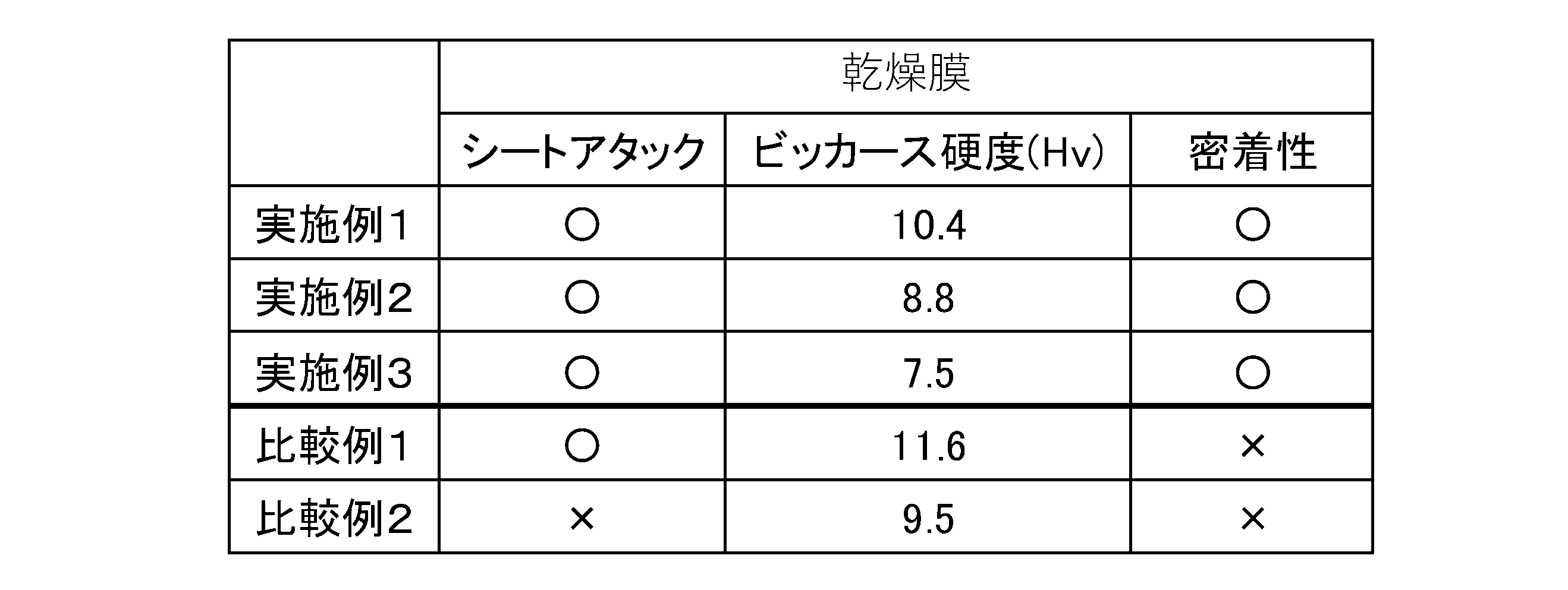
表1、2から明らかなように、本実施形態の導電性ペーストを用いた実施例1~3では、シートアタックの発生が無く、膜硬度が低く、密着性が向上していることがわかる。
[1] 導電性金属粉末、セラミック粉末、バインダー樹脂、添加剤、及び有機溶剤を含む導電性ペーストであって、
前記有機溶剤が、(A)ジヒドロターピニルアセテート、イソボルニルアセテート、イソボルニルプロピオネート、イソボルニルブチレート及びイソボルニルイソブチレートから選ばれる少なくとも1種と、(B)エチレングリコールモノブチルエーテルアセテート及びジプロピレングリコールメチルエーテルアセテートから選ばれる少なくとも1種とを含み、
前記添加剤が、リン酸ポリエステルを導電性ペースト全体量に対し0質量%を超え2.0質量%以下含有する、導電性ペースト。
(測定条件)
マイクロビッカース硬度計を用いて試験力98mNの条件で前記乾燥膜の表面のビッカース硬度を測定する。
10 セラミック積層体
11 内部電極層
12 誘電体層
20 外部電極
21 外部電極層
22 メッキ層
Claims (10)
- 導電性金属粉末、セラミック粉末、バインダー樹脂、添加剤、及び有機溶剤を含む導電性ペーストであって、
前記有機溶剤が、(A)ジヒドロターピニルアセテート、イソボルニルアセテート、イソボルニルプロピオネート、イソボルニルブチレート及びイソボルニルイソブチレートから選ばれる少なくとも1種と、(B)エチレングリコールモノブチルエーテルアセテート及びジプロピレングリコールメチルエーテルアセテートから選ばれる少なくとも1種とを含み、
前記添加剤が、リン酸ポリエステルを導電性ペースト全体量に対し0質量%を超え2.0質量%以下含有する、導電性ペースト。 - 前記導電性金属粉末が、Ni、Pd、Pt、Au、Ag、Cu、およびこれらの合金から選ばれる1種の金属粉末からなる、請求項1に記載の導電性ペースト。
- 前記セラミック粉末が、ペロブスカイト型酸化物であるチタン酸バリウム(BaTiO3)である請求項1又は2に記載の導電性ペースト。
- 前記セラミック粉末が、ペロブスカイト型酸化物強誘電体である、請求項1又は2に記載の導電性ペースト。
- 積層セラミックデバイスの内部電極層用の導電性ペーストであって、前記積層セラミックデバイスは、誘電体グリーンシートを用いて形成される誘電体層、及び、前記内部電極層を有し、前記誘電体グリーンシートに含まれる誘電体セラミック粉末と、前記導電性ペーストに含まれる前記セラミック粉末とが同一組成の粉末である、請求項1に記載の導電性ペースト。
- 前記導電性ペーストを、チタン酸バリウムおよびポリビニルブチラール樹脂を含むグリーンシート上にWET膜厚38μmで塗布し、75℃で20分乾燥させて乾燥膜を得た場合、下記の条件で測定されるビッカース硬度が5Hv以上11Hv以下である、請求項1又は2に記載の導電性ペースト。
(測定条件)
マイクロビッカース硬度計を用いて試験力98mNの条件で前記乾燥膜の表面のビッカース硬度を測定する。 - 請求項1又は2に記載の導電性ペーストを用いて形成される乾燥膜。
- 請求項7に記載の乾燥膜を用いて形成される積層セラミックコンデンサの内部電極。
- 請求項8に記載の内部電極と、誘電体グリーンシートを用いて形成される誘電体層とを有する積層セラミックコンデンサ。
- 前記誘電体グリーンシートの厚さが、3μm以下であることを特徴とする請求項9に記載の積層セラミックコンデンサ。
Priority Applications (2)
| Application Number | Priority Date | Filing Date | Title |
|---|---|---|---|
| KR1020247039670A KR20250002690A (ko) | 2022-07-08 | 2023-07-06 | 도전성 페이스트, 건조막, 내부 전극 및 적층 세라믹 콘덴서 |
| CN202380051530.6A CN119547166A (zh) | 2022-07-08 | 2023-07-06 | 导电性浆料、干燥膜、内部电极以及叠层陶瓷电容器 |
Applications Claiming Priority (2)
| Application Number | Priority Date | Filing Date | Title |
|---|---|---|---|
| JP2022110487A JP7831167B2 (ja) | 2022-07-08 | 2022-07-08 | 導電性ペースト、乾燥膜、内部電極、及び、積層セラミックコンデンサ |
| JP2022-110487 | 2022-07-08 |
Publications (1)
| Publication Number | Publication Date |
|---|---|
| WO2024010075A1 true WO2024010075A1 (ja) | 2024-01-11 |
Family
ID=89453625
Family Applications (1)
| Application Number | Title | Priority Date | Filing Date |
|---|---|---|---|
| PCT/JP2023/025203 Ceased WO2024010075A1 (ja) | 2022-07-08 | 2023-07-06 | 導電性ペースト、乾燥膜、内部電極、及び、積層セラミックコンデンサ |
Country Status (5)
| Country | Link |
|---|---|
| JP (1) | JP7831167B2 (ja) |
| KR (1) | KR20250002690A (ja) |
| CN (1) | CN119547166A (ja) |
| TW (1) | TW202414441A (ja) |
| WO (1) | WO2024010075A1 (ja) |
Cited By (1)
| Publication number | Priority date | Publication date | Assignee | Title |
|---|---|---|---|---|
| CN121649384A (zh) * | 2025-11-18 | 2026-03-13 | 深圳市先进连接科技有限公司 | 烧结金属材料及其制备方法与应用 |
Citations (4)
| Publication number | Priority date | Publication date | Assignee | Title |
|---|---|---|---|---|
| JP2014515160A (ja) * | 2011-03-29 | 2014-06-26 | サン ケミカル コーポレイション | ワックスチクソトロープ剤を含有する高いアスペクト比のスクリーン印刷可能な厚膜ペースト組成物 |
| WO2019107500A1 (ja) * | 2017-11-30 | 2019-06-06 | 住友金属鉱山株式会社 | 導電性ペースト、電子部品、及び積層セラミックコンデンサ |
| JP2019102393A (ja) * | 2017-12-07 | 2019-06-24 | 住友金属鉱山株式会社 | 積層セラミックコンデンサ用ニッケルペースト |
| WO2020144746A1 (ja) * | 2019-01-08 | 2020-07-16 | 住友金属鉱山株式会社 | 積層セラミックコンデンサ用ニッケルペースト |
Family Cites Families (1)
| Publication number | Priority date | Publication date | Assignee | Title |
|---|---|---|---|---|
| JP2017143202A (ja) | 2016-02-12 | 2017-08-17 | 住友金属鉱山株式会社 | 内部電極用ペーストとその製造方法、及び積層セラミックコンデンサ |
-
2022
- 2022-07-08 JP JP2022110487A patent/JP7831167B2/ja active Active
-
2023
- 2023-07-06 CN CN202380051530.6A patent/CN119547166A/zh active Pending
- 2023-07-06 KR KR1020247039670A patent/KR20250002690A/ko active Pending
- 2023-07-06 WO PCT/JP2023/025203 patent/WO2024010075A1/ja not_active Ceased
- 2023-07-07 TW TW112125425A patent/TW202414441A/zh unknown
Patent Citations (4)
| Publication number | Priority date | Publication date | Assignee | Title |
|---|---|---|---|---|
| JP2014515160A (ja) * | 2011-03-29 | 2014-06-26 | サン ケミカル コーポレイション | ワックスチクソトロープ剤を含有する高いアスペクト比のスクリーン印刷可能な厚膜ペースト組成物 |
| WO2019107500A1 (ja) * | 2017-11-30 | 2019-06-06 | 住友金属鉱山株式会社 | 導電性ペースト、電子部品、及び積層セラミックコンデンサ |
| JP2019102393A (ja) * | 2017-12-07 | 2019-06-24 | 住友金属鉱山株式会社 | 積層セラミックコンデンサ用ニッケルペースト |
| WO2020144746A1 (ja) * | 2019-01-08 | 2020-07-16 | 住友金属鉱山株式会社 | 積層セラミックコンデンサ用ニッケルペースト |
Cited By (1)
| Publication number | Priority date | Publication date | Assignee | Title |
|---|---|---|---|---|
| CN121649384A (zh) * | 2025-11-18 | 2026-03-13 | 深圳市先进连接科技有限公司 | 烧结金属材料及其制备方法与应用 |
Also Published As
| Publication number | Publication date |
|---|---|
| JP2024008536A (ja) | 2024-01-19 |
| CN119547166A (zh) | 2025-02-28 |
| TW202414441A (zh) | 2024-04-01 |
| KR20250002690A (ko) | 2025-01-07 |
| JP7831167B2 (ja) | 2026-03-17 |
Similar Documents
| Publication | Publication Date | Title |
|---|---|---|
| JP7750318B2 (ja) | 導電性ペースト、電子部品、及び積層セラミックコンデンサ | |
| TWI798292B (zh) | 導電性漿料、電子零件及層積陶瓷電容器 | |
| KR102737839B1 (ko) | 도전성 페이스트, 전자 부품, 및 적층 세라믹 콘덴서 | |
| WO2020137290A1 (ja) | 導電性ペースト、電子部品、及び積層セラミックコンデンサ | |
| CN113396458B (zh) | 导电性浆料、电子部件以及叠层陶瓷电容器 | |
| WO2022092045A1 (ja) | グラビア印刷用導電性ペースト、電子部品、及び積層セラミックコンデンサ | |
| TWI798301B (zh) | 導電性漿料、電子零件、及層積陶瓷電容器 | |
| JP7831167B2 (ja) | 導電性ペースト、乾燥膜、内部電極、及び、積層セラミックコンデンサ | |
| TWI810336B (zh) | 導電性漿料、電子零件以及積層陶瓷電容器 | |
| CN115210823B (zh) | 导电性浆料、电子部件以及叠层陶瓷电容器 | |
| JP2021064607A (ja) | 導電性ペースト、電子部品、及び、積層セラミックコンデンサ | |
| JP7586088B2 (ja) | 導電性組成物、導電性ペースト、電子部品、及び積層セラミックコンデンサ |
Legal Events
| Date | Code | Title | Description |
|---|---|---|---|
| 121 | Ep: the epo has been informed by wipo that ep was designated in this application |
Ref document number: 23835606 Country of ref document: EP Kind code of ref document: A1 |
|
| ENP | Entry into the national phase |
Ref document number: 20247039670 Country of ref document: KR Kind code of ref document: A |
|
| WWE | Wipo information: entry into national phase |
Ref document number: 202380051530.6 Country of ref document: CN |
|
| NENP | Non-entry into the national phase |
Ref country code: DE |
|
| WWP | Wipo information: published in national office |
Ref document number: 202380051530.6 Country of ref document: CN |
|
| 122 | Ep: pct application non-entry in european phase |
Ref document number: 23835606 Country of ref document: EP Kind code of ref document: A1 |