WO2024009790A1 - 検出装置 - Google Patents
検出装置 Download PDFInfo
- Publication number
- WO2024009790A1 WO2024009790A1 PCT/JP2023/023173 JP2023023173W WO2024009790A1 WO 2024009790 A1 WO2024009790 A1 WO 2024009790A1 JP 2023023173 W JP2023023173 W JP 2023023173W WO 2024009790 A1 WO2024009790 A1 WO 2024009790A1
- Authority
- WO
- WIPO (PCT)
- Prior art keywords
- light
- detection device
- optical sensor
- waveform data
- light source
- Prior art date
- Legal status (The legal status is an assumption and is not a legal conclusion. Google has not performed a legal analysis and makes no representation as to the accuracy of the status listed.)
- Ceased
Links
Images







Classifications
-
- A—HUMAN NECESSITIES
- A61—MEDICAL OR VETERINARY SCIENCE; HYGIENE
- A61B—DIAGNOSIS; SURGERY; IDENTIFICATION
- A61B5/00—Measuring for diagnostic purposes; Identification of persons
- A61B5/0059—Measuring for diagnostic purposes; Identification of persons using light, e.g. diagnosis by transillumination, diascopy, fluorescence
- A61B5/0077—Devices for viewing the surface of the body, e.g. camera, magnifying lens
-
- A—HUMAN NECESSITIES
- A61—MEDICAL OR VETERINARY SCIENCE; HYGIENE
- A61B—DIAGNOSIS; SURGERY; IDENTIFICATION
- A61B5/00—Measuring for diagnostic purposes; Identification of persons
- A61B5/68—Arrangements of detecting, measuring or recording means, e.g. sensors, in relation to patient
- A61B5/6801—Arrangements of detecting, measuring or recording means, e.g. sensors, in relation to patient specially adapted to be attached to or worn on the body surface
- A61B5/6813—Specially adapted to be attached to a specific body part
- A61B5/6825—Hand
- A61B5/6826—Finger
-
- A—HUMAN NECESSITIES
- A61—MEDICAL OR VETERINARY SCIENCE; HYGIENE
- A61B—DIAGNOSIS; SURGERY; IDENTIFICATION
- A61B5/00—Measuring for diagnostic purposes; Identification of persons
- A61B5/145—Measuring characteristics of blood in vivo, e.g. gas concentration or pH-value ; Measuring characteristics of body fluids or tissues, e.g. interstitial fluid or cerebral tissue
- A61B5/1455—Measuring characteristics of blood in vivo, e.g. gas concentration or pH-value ; Measuring characteristics of body fluids or tissues, e.g. interstitial fluid or cerebral tissue using optical sensors, e.g. spectral photometrical oximeters
- A61B5/14551—Measuring characteristics of blood in vivo, e.g. gas concentration or pH-value ; Measuring characteristics of body fluids or tissues, e.g. interstitial fluid or cerebral tissue using optical sensors, e.g. spectral photometrical oximeters for measuring blood gases
- A61B5/14552—Details of sensors specially adapted therefor
-
- H—ELECTRICITY
- H10—SEMICONDUCTOR DEVICES; ELECTRIC SOLID-STATE DEVICES NOT OTHERWISE PROVIDED FOR
- H10F—INORGANIC SEMICONDUCTOR DEVICES SENSITIVE TO INFRARED RADIATION, LIGHT, ELECTROMAGNETIC RADIATION OF SHORTER WAVELENGTH OR CORPUSCULAR RADIATION
- H10F55/00—Radiation-sensitive semiconductor devices covered by groups H10F10/00, H10F19/00 or H10F30/00 being structurally associated with electric light sources and electrically or optically coupled thereto
-
- A—HUMAN NECESSITIES
- A61—MEDICAL OR VETERINARY SCIENCE; HYGIENE
- A61B—DIAGNOSIS; SURGERY; IDENTIFICATION
- A61B2562/00—Details of sensors; Constructional details of sensor housings or probes; Accessories for sensors
- A61B2562/02—Details of sensors specially adapted for in-vivo measurements
- A61B2562/0233—Special features of optical sensors or probes classified in A61B5/00
- A61B2562/0238—Optical sensor arrangements for performing transmission measurements on body tissue
-
- A—HUMAN NECESSITIES
- A61—MEDICAL OR VETERINARY SCIENCE; HYGIENE
- A61B—DIAGNOSIS; SURGERY; IDENTIFICATION
- A61B2562/00—Details of sensors; Constructional details of sensor housings or probes; Accessories for sensors
- A61B2562/18—Shielding or protection of sensors from environmental influences, e.g. protection from mechanical damage
- A61B2562/185—Optical shielding, e.g. baffles
-
- A—HUMAN NECESSITIES
- A61—MEDICAL OR VETERINARY SCIENCE; HYGIENE
- A61B—DIAGNOSIS; SURGERY; IDENTIFICATION
- A61B5/00—Measuring for diagnostic purposes; Identification of persons
- A61B5/145—Measuring characteristics of blood in vivo, e.g. gas concentration or pH-value ; Measuring characteristics of body fluids or tissues, e.g. interstitial fluid or cerebral tissue
- A61B5/14535—Measuring characteristics of blood in vivo, e.g. gas concentration or pH-value ; Measuring characteristics of body fluids or tissues, e.g. interstitial fluid or cerebral tissue for measuring haematocrit
Definitions
- the present invention relates to a detection device.
- detection devices equipped with a light source and a sensor section have been developed in recent years.
- a light source and a sensor section are arranged so as to sandwich an object to be detected.
- light is irradiated onto the skin from a light source, and the light enters the body. Then, the light passes through blood, muscle tissue, etc. in the body, is further emitted outside the body, and is received by the sensor section.
- the optical sensor when measuring biological information such as pulse rate and blood oxygen saturation (SpO 2 ) using an optical sensor, if there is an external light component in addition to the light from the measurement light source, the optical sensor may not be able to match the desired wavelength.
- the detection device may detect a different wavelength. Therefore, in a detection device using an optical sensor, it has been desired to suppress the influence of external light.
- An object of the present invention is to provide a detection device that can suppress the influence of external light when measuring using an optical sensor.
- a detection device includes a light source, a plurality of optical sensors arranged so as to be able to receive light from the light source and having different sizes of light receiving areas, and electrically connected to each of the plurality of optical sensors.
- a detection circuit for detecting waveform data capable of identifying the amount of light received by each of the plurality of optical sensors; and at least one of the plurality of waveform data detected from the plurality of optical sensors, the amplitude of the waveform satisfying a selection condition.
- a control circuit that selects one waveform data.
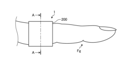
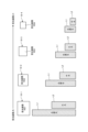
- FIG. 1 is a schematic diagram illustrating an example of the external appearance of a detection device according to an embodiment when a finger is placed inside the detection device when viewed from the side of the housing.
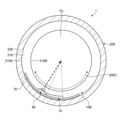
- FIG. 2 is a schematic cross-sectional view taken along the line AA shown in FIG.
- FIG. 3 is a schematic plan view showing a configuration example of the optical sensor and light source of the detection device shown in FIG. 1.
- FIG. 4 is a schematic cross-sectional view showing an example of the laminated structure of the optical sensor taken along the BB cross section shown in FIG.
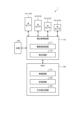
- FIG. 5 is a block diagram showing a configuration example of a detection device according to an embodiment.
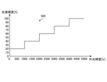
- FIG. 6 is a diagram showing an example of table data for determining light source brightness from the brightness of external light.
- FIG. 7 is a diagram for explaining an example of the sensor light reception ratio of the reference optical sensor.
- FIG. 8 is a diagram for explaining an example of the relationship between the light-receiving area of the optical sensor, the light source light, and the external light.
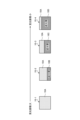
- FIG. 9 is a diagram illustrating an example of a detection device selection method according to the embodiment.
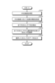
- FIG. 10 is a flowchart illustrating an example of a processing procedure executed by the detection device according to the embodiment.
- FIG. 11 is a schematic plan view showing a configuration example of an optical sensor and a light source of a detection device according to a modification of the embodiment.
- FIG. 12 is a diagram showing another configuration example of the plurality of optical sensors shown in FIG. 11.
- FIG. 13 is a diagram for explaining another example of the arrangement relationship between a plurality of optical sensors and a light source.
- FIG. 14 is a schematic plan view showing a configuration example of an optical sensor and a light source of a detection device according to a modification of the embodiment.
- FIG. 1 is a schematic diagram illustrating an example of the external appearance of a detection device according to an embodiment when a finger is placed inside the detection device when viewed from the side of the housing.
- FIG. 2 is a schematic cross-sectional view taken along the line AA shown in FIG.
- FIG. 3 is a schematic plan view showing a configuration example of the optical sensor and light source of the detection device shown in FIG. 1.
- FIG. 4 is a schematic cross-sectional view showing an example of the laminated structure of the optical sensor taken along the BB cross section shown in FIG. Note that in FIG. 2, only the basic configuration of the detection device according to the embodiment is illustrated, and other configurations are omitted.
- the detection device 1 shown in FIG. 1 is a ring-shaped device that is detachable from the human body, and is attached to the finger Fg of the human body.
- the fingers Fg include the thumb, index finger, middle finger, ring finger, little finger, and the like.
- the human body is a person to be authenticated whose identity is verified by the detection device 1 .
- the detection device 1 can detect biological information regarding a living body from the finger Fg attached.
- the finger Fg is an example of a measurement target.
- the measurement target is a living body or a part of a living body, and is a measuring object.
- the detection device 1 is made into a ring or a wristband so that it can be easily carried by the user. In the following description, it is assumed that the detection device 1 is used as a ring. Note that the detection device 1 can use the detected biometric information to authenticate the person to be authenticated.
- the detection device 1 includes a housing 200, a light source 60, and a plurality of optical sensors 10.
- the detection device 1 is a device that includes a battery (not shown) inside a casing 200 and operates using power from the battery.
- the housing 200 is formed in a ring shape that can be attached to a finger Fg, and is an attachment member that is attached to a living body.
- the housing 200 includes a first housing 210 and a second housing 220.
- the housing 200 is formed into a ring shape by integrating a first housing 210 and a second housing 220.
- the first housing 210 is a member that comes into contact with the human body to which the housing 200 is attached.
- the first housing 210 accommodates a light source 60, a plurality of optical sensors 10, etc. therein.
- the first housing 210 is formed into a ring shape using a housing material such as light-transmissive synthetic resin or silicone, for example.
- the second housing 220 has a surface of the housing 200 that covers the outer peripheral surface 210A of the first housing 210.
- the second housing 220 is formed into a ring shape using a member such as metal or non-transparent synthetic resin.
- the housing 200 houses a flexible printed circuit board 70 on which a light source 60, a plurality of optical sensors 10, etc. are mounted, inside a first housing 210.
- the flexible printed circuit board 70 is housed inside the casing 200 by, for example, forming the casing 200 by filling the periphery of the flexible printed circuit board 70 in a ring shape with a filling member in a mold.
- the flexible printed circuit board 70 is formed into a deformable band shape.
- an optical sensor 10 On the flexible printed circuit board 70, an optical sensor 10, a light source 60, a detection control circuit 110, and an MCU (Micro Controller Unit) 120 are mounted.
- the flexible printed circuit board 70 electrically connects the plurality of optical sensors 10 and the detection control circuit 110.
- the flexible printed circuit board 70 electrically connects the detection control circuit 110 and the MCU 120 via wiring 71.
- the flexible printed circuit board 70 electrically connects the detection control circuit 110 and the light source 60 via wiring 72.
- the first direction Dx is one direction in a plane parallel to the flexible printed circuit board 70, and is the same direction as the circumferential direction 200C.
- the second direction Dy is one direction within a plane parallel to the flexible printed circuit board 70, and is a direction perpendicular to the first direction Dx. Note that the second direction Dy may not be perpendicular to the first direction Dx but may intersect with the first direction Dx.
- the third direction Dz is a direction orthogonal to the first direction Dx and the second direction Dy.
- the third direction Dz is the normal direction of the flexible printed circuit board 70.
- plane view refers to the positional relationship when viewed from a direction perpendicular to the flexible printed circuit board 70.
- the flexible printed circuit board 70 arranges a plurality of optical sensors 10 having different lengths in the circumferential direction 200C along the first direction Dx in a row in the second direction Dy, which is the width direction 200D of the housing 200. are doing.
- Each of the plurality of optical sensors 10 has a larger area in plan view as the length in the circumferential direction 200C is longer.
- the flexible printed circuit board 70 has an optical sensor 10-2, an optical sensor 10-3, and an optical sensor whose length gradually becomes shorter from one end 70A to the other end 70B in the second direction Dy. They are arranged in the order of 10-4.
- the flexible printed circuit board 70 has a plurality of optical sensors 10 arranged near the light source 60. Thereby, the plurality of optical sensors 10 can detect the light emitted by the light source 60 and reflected by the finger Fg (human body). The plurality of optical sensors 10 detect the intensity of light and convert it into an electrical signal.
- the light source 60 is provided inside the first casing 210 of the casing 200, and is configured to be able to irradiate light toward the center of the casing 200.
- the light source 60 for example, an inorganic LED (Light Emitting Diode) or an organic EL (OLED) is used.
- the light source 60 emits light of a predetermined wavelength.
- the light source 60 has a plurality of LEDs so as to be able to emit infrared light, red light, and green light.
- the light source 60 is configured to selectively emit infrared light, red light, and green light.
- the light source 60 includes a first light source 61 having an LED that emits infrared light, and a second light source 62 having an LED that emits red light.
- the first light source 61 and the second light source 62 are mounted on the flexible printed circuit board 70 so that they are equidistant from the optical sensor 10-1, the optical sensor 10-2, the optical sensor 10-3, and the optical sensor 10-4. By providing this, external light components are effectively reduced.
- the first light source 61 and the second light source 62 may be realized by, for example, one LED or a plurality of LEDs.
- the light emitted from the light source 60 is reflected by the surface of the object to be detected, such as the finger Fg, and enters the optical sensor 10.
- the light emitted from the light source 60 may be reflected inside the finger Fg or the like, or may be transmitted through the finger Fg or the like and enter the plurality of photodiodes PD of the optical sensor 10.
- the detection device 1 can detect information regarding a living body inside the finger Fg or the like.
- the information regarding the living body includes, for example, pulse waves and pulses of fingers and palms. That is, the detection device 1 may be configured as a vein detection device that detects biological information such as veins.
- the plurality of optical sensors 10 are arranged side by side inside the first casing 210 of the casing 200 and are sensors capable of detecting light incident from the irradiation side of the light source 60.
- the irradiation side of the light source 60 is the side that irradiates the finger Fg to be measured, which is equipped with the housing 200.
- the irradiation side of the light source 60 housed inside the ring-shaped housing 200 is the side that irradiates from the inside of the housing 200 to the outside, and is the inner circumferential surface of the housing 200 that the finger Fg to be measured approaches. 210B side (see FIG. 2).
- the plurality of optical sensors 10 detect light emitted by the light source 60 and reflected by the finger Fg, directly incident light, and the like.
- the plurality of optical sensors 10 are organic photodiodes (OPDs). As shown in FIG. 3, the plurality of optical sensors 10 are provided inside the housing 200 in a state where they are lined up along the light source 60 in the width direction 200D (second direction Dy) of the housing 200.
- OPDs organic photodiodes
- the plurality of optical sensors 10 include an optical sensor 10-1, an optical sensor 10-2, an optical sensor 10-3, and an optical sensor 10-4.
- optical sensor 10-1 when there is no need to distinguish between optical sensor 10-1, optical sensor 10-2, optical sensor 10-3, and optical sensor 10-4, they will simply be referred to as optical sensor 10.
- Each of the plurality of optical sensors 10 has a light receiving area 10A having a different size.
- the size includes light sensitivity.
- the light receiving area 10A is a planar area of the optical sensor 10 that receives light.
- the plurality of optical sensors 10 have the same length in the width direction 200D of the housing 200.
- the light receiving area 10A is formed in a rectangular shape extending along the circumferential direction 200C, but the shape is not limited to this, and a plurality of shapes may be arranged side by side.
- the light-receiving area 10A has the longest length in the circumferential direction 200C, and the light-receiving area is the largest.
- the length of the light receiving area 10A is shorter than that of the optical sensor 10-1 in the circumferential direction 200C, and the light receiving area is smaller than that of the optical sensor 10-1.
- the length of the light receiving area 10A is shorter than that of the optical sensor 10-2, and the light receiving area is smaller than that of the optical sensor 10-2.
- the length of the light receiving area 10A is shorter than that of the optical sensor 10-3 in the circumferential direction 200C, and the light receiving area is smaller than that of the optical sensor 10-3.
- the optical sensor 10-4 is approximately half the size of the optical sensor 10-1.
- the optical sensor 10 has an organic photodiode. As shown in FIG. 4, the optical sensor 10 includes a sensor substrate 21 and a photodiode PD. In this embodiment, the optical sensor 10 further includes wiring 26 and an insulating layer 27. The insulating layer 27 is provided on the sensor substrate 21 so as to cover the wiring 26 . The insulating layer 27 may be an inorganic insulating film or an organic insulating film. Note that the wiring 26 may be formed in the same layer as the lower electrode 11.
- the photodiode PD is provided on the insulating layer 27.
- Photodiode PD includes a lower electrode 11, a lower buffer layer 12, an active layer 13, an upper buffer layer 14, and an upper electrode 15.
- the photodiode PD includes a lower electrode 11, a lower buffer layer 12 (hole transport layer), an active layer 13, an upper buffer layer 14 (electron transport layer), and an upper electrode 15 in a third direction Dz perpendicular to the sensor substrate 21. Laminated in order.
- the lower electrode 11 is an anode electrode of the photodiode PD, and is formed of a conductive material having light-transmitting properties, such as ITO (Indium Tin Oxide), for example.
- the active layer 13 has characteristics (for example, voltage-current characteristics and resistance value) that change depending on the irradiated light.
- An organic material is used as the material for the active layer 13.
- the active layer 13 is a bulk heterostructure in which a p-type organic semiconductor and an n-type fullerene derivative (PCBM), which is an n-type organic semiconductor, coexist.
- PCBM n-type fullerene derivative
- low-molecular organic materials C60 (fullerene), PCBM (Phenyl C61-butyric acid methyl ester), CuPc (Copper Phthalocyanine), F16CuPc (fluorinated copper phthalocyanine) can be used.
- rubrene 5,6,11,12-tetraphenyltetracene
- PDI a derivative of Perylene
- the active layer 13 can be formed using these low-molecular organic materials by vapor deposition (dry process).
- the active layer 13 may be, for example, a laminated film of CuPc and F16CuPc, or a laminated film of rubrene and C60.
- the active layer 13 can also be formed by a wet process.
- the active layer 13 is made of a combination of the above-mentioned low-molecular organic material and high-molecular organic material.
- the polymeric organic material for example, P3HT (poly(3-hexylthiophene)), F8BT (F8-alt-benzothiadiazole), etc. can be used.
- the active layer 13 can be a film containing a mixture of P3HT and PCBM, or a film containing a mixture of F8BT and PDI.
- the lower buffer layer 12 is a hole transport layer.
- Upper buffer layer 14 is an electron transport layer.
- the lower buffer layer 12 and the upper buffer layer 14 are provided so that holes and electrons generated in the active layer 13 can easily reach the lower electrode 11 or the upper electrode 15.
- the lower buffer layer 12 (hole transport layer) is provided in direct contact with the lower electrode 11 and also in the region between adjacent lower electrodes 11 .
- the active layer 13 is in direct contact with the top of the lower buffer layer 12 .
- the material of the hole transport layer is a metal oxide layer. Tungsten oxide (WO 3 ), molybdenum oxide, or the like is used as the metal oxide layer.
- the upper buffer layer 14 (electron transport layer) is in direct contact with the top of the active layer 13, and the top electrode 15 is in direct contact with the top of the top buffer layer 14.
- Ethoxylated polyethyleneimine (PEIE) is used as the material for the electron transport layer.
- the materials and manufacturing methods for the lower buffer layer 12, active layer 13, and upper buffer layer 14 are merely examples, and other materials and manufacturing methods may be used.
- the lower buffer layer 12 and the upper buffer layer 14 are not limited to single-layer films, and may be formed as laminated films including an electron blocking layer and a hole blocking layer.
- the upper electrode 15 is provided on the upper buffer layer 14.
- the upper electrode 15 is a cathode electrode of the photodiode PD, and is continuously formed over the entire optical sensor 10. In other words, the upper electrode 15 is continuously provided on the plurality of photodiodes PD.
- the upper electrode 15 faces the plurality of lower electrodes 11 with the lower buffer layer 12, the active layer 13, and the upper buffer layer 14 in between.
- the upper electrode 15 is made of, for example, a light-transmitting conductive material such as ITO or IZO.
- the upper electrode 15 is electrically connected to a power supply circuit (not shown).
- Each of the plurality of optical sensors 10 is electrically connected to the detection control circuit 110 via wiring 26 provided on the flexible printed circuit board 70.
- the detection control circuit 110 is electrically connected to the lower electrode 11 of the optical sensor 10 via the plurality of wirings 26.
- the photodiodes PD of the optical sensor 10 each output an electric signal corresponding to the light irradiated thereon to the detection control circuit 110 as a detection signal Vdet.
- each of the plurality of optical sensors 10 outputs an electric signal corresponding to the light irradiated onto the light receiving area 10A to the detection control circuit 110 as the detection signal Vdet.
- the detection control circuit 110 supplies control signals to the photodiodes PD of the plurality of optical sensors 10 to control the detection operation, and detects the detected object for each of the plurality of optical sensors 10 based on the detection signal Vdet from the photodiode PD.
- the detection control circuit 110 includes, for example, an analog front end circuit (AFE).
- the detection control circuit 110 includes a signal processing circuit having at least the functions of a detection signal amplification section and an A/D conversion section.
- the detection signal amplification section amplifies the detection signal Vdet.
- the A/D conversion section converts the analog signal output from the detection signal amplification section into a digital signal.
- the MCU 120 is electrically connected to detection control circuit 110.
- the MCU 120 executes processing based on the detection result of the detection control circuit 110.
- the MCU 120 can execute a process of calculating blood oxygen saturation (SpO 2 ) from the ratio of hemoglobin absorbance at the wavelength detected by the detection control circuit 110.
- blood oxygen saturation (SpO 2 ) is the ratio of the amount of oxygen actually bound to hemoglobin to the total amount of oxygen, assuming that oxygen is bound to all of the hemoglobin in the blood.
- the MCU 120 can display biological information including blood oxygen saturation and the like on a display device or transmit it via a communication device.
- the MCU 120 has a function of comparing the information regarding the living body detected by the detection control circuit 110 with authentication information stored in advance, and authenticating the person to be authenticated based on the comparison result.
- the MCU 120 has a function of controlling the transmission of information regarding the detected living body to an external device via a communication device (not shown).
- the configuration example of the detection device 1 according to the present embodiment has been described above.
- or FIG. 4 is an example to the last, and the structure of the detection apparatus 1 based on this embodiment is not limited to the example which concerns.
- the configuration of the detection device 1 according to this embodiment can be flexibly modified according to specifications and operation.
- FIG. 5 is a block diagram showing a configuration example of the detection device 1 according to the embodiment.
- FIG. 6 is a diagram showing an example of table data for determining light source brightness from the brightness of external light.
- the detection device 1 includes four optical sensors 10-1, 10-2, 10-3, and 10-4, a detection control circuit 110, and an MCU 120.
- Detection control circuit 110 is an example of a detection circuit.
- the optical sensor 10 is an optical sensor that has a photodiode PD that is a photoelectric conversion element.
- the photodiode PD included in the optical sensor 10 outputs an electric signal corresponding to the irradiated light to the detection control circuit 110 as a detection signal Vdet. Further, the optical sensor 10 detects light according to a gate drive signal supplied from the detection control circuit 110.
- the detection control circuit 110 includes a drive control circuit 111 and a detection circuit 112.
- the drive control circuit 111 is a circuit that supplies control signals to each of the plurality of optical sensors 10 and controls their operations.
- the drive control circuit 111 supplies various control signals such as a start signal STV, a clock signal CK, and a reset signal RST1 to the plurality of optical sensors 10.
- the drive control circuit 111 supplies various control signals to the light source 60 in response to instructions from the MCU 120 to control lighting and non-lighting.
- the detection circuit 112 is, for example, an analog front end circuit (AFE).
- the detection circuit 112 detects each analog signal from the plurality of optical sensors 10.
- the detection circuit 112 can select a signal line to be detected using a switch circuit that selects a plurality of signal lines sequentially or simultaneously.
- the detection circuit 112 can output the detected analog signal to the MCU 120 as a detection signal of the optical sensor 10.
- the detection circuit 112 can output detection signals from each of the four optical sensors 10-1, 10-2, 10-3, and 10-4 to the MCU 120.
- the MCU 120 includes a control circuit 121, a memory circuit 122, and an external light detection circuit 123.
- the control circuit 121 has a function of acquiring detection signals detected simultaneously by the plurality of optical sensors 10 and converting the detection signals from analog signals to digital signals.
- the control circuit 121 stores waveform data indicated by the acquired detection signal in the storage circuit 122 in association with the optical sensor 10 .
- the control circuit 121 selects waveform data whose waveform amplitude satisfies the selection condition from among the waveform data acquired from the plurality of optical sensors 10.
- the control circuit 121 selects, from the plurality of waveform data, the waveform data having the largest average value of the plurality of amplitudes in the waveform indicated by the waveform data.
- the amplitude includes the peak-to-peak distance of the waveform, the distance from the center of the waveform to the maximum displacement, and the like.
- control circuit 121 calculates the average value of a predetermined number of peak-to-peak amplitudes in the waveform indicated by the waveform data, and selects the waveform data with the largest average value from among the plurality of waveform data.
- the predetermined number is set, for example, to equalize the number of comparison target amplitudes in a plurality of waveform data.
- the control circuit 121 selects the waveform data according to a predetermined priority order.
- a plurality of average values being the same means that the average values are equal or that the average values are within an error range.
- the predetermined priorities include, for example, priorities assigned to the four optical sensors 10-1, 10-2, 10-3, and 10-4.
- the predetermined priority order is set such that the priority order gradually decreases in the order of optical sensor 10-1, optical sensor 10-2, optical sensor 10-3, and optical sensor 10-4. .
- control circuit 121 selects the waveform data of the optical sensor 10 having the smaller area of the light receiving region 10A. Note that an example of selection of the control circuit 121 will be described later.
- the storage circuit 122 temporarily stores the signal calculated by the control circuit 121.
- the memory circuit 122 may be, for example, a RAM (Random Access Memory), a register circuit, or the like.
- the storage circuit 122 can store information such as selection conditions used by the control circuit 121.
- the external light detection circuit 123 has a function of detecting the external light intensity of the detection device 1.
- the external light detection circuit 123 detects the external light intensity based on detection signals detected simultaneously by the plurality of optical sensors 10.
- the external light detection circuit 123 detects external light intensity based on waveform data from any one of the plurality of optical sensors 10.
- the external light detection circuit 123 uses waveform data of the optical sensor 10 having the largest light receiving area 10A among the plurality of optical sensors 10.
- the external light detection circuit 123 supplies external light intensity information including the value of the detected external light intensity to the control circuit 121.
- the control circuit 121 When the control circuit 121 receives the external light intensity information from the external light detection circuit 123, it sets the brightness of the light source 60 according to the external light intensity of the external light intensity information.
- the detection device 1 stores in the storage circuit 122 table data 500 for determining light source brightness from the brightness of external light.
- the horizontal axis represents external light brightness [lx]
- the vertical axis represents light source brightness [%].
- the table data 500 is a table that associates external light brightness and light source brightness in a stepwise manner and calculates the light source brightness from the external light brightness.
- the control circuit 121 sets the brightness of the light source 60 to 20% when the external light intensity from the external light detection circuit 123 is smaller than 1000 lx, and when the external light intensity from the external light detection circuit 123 is 4000 lx or more, the control circuit 121 sets the brightness of the light source 60 to 20%. Set the brightness of 60 to 20%.
- the control circuit 121 sets the brightness of the light source 60 in stages when the external light intensity detected by the external light detection circuit 123 is greater than or equal to 1000 lx and less than 4000 lx. Note that the external light detection circuit 123 may be included in the control circuit 121.
- FIG. 7 is a diagram for explaining an example of the sensor light reception ratio of the reference optical sensor.
- the detection device 1 detects a component of a wavelength different from the desired wavelength to the detection circuit 112.
- the effective signal value is buried in the external light component.
- the higher the external light level is, the higher the brightness of the light source 60 is required.
- the amount of light source light L1 received by the detection device 1 increases more than the amount of external light L2 received, but it falls outside the dynamic range of the AD converter. I end up. That is, in the detection device 1, when the brightness of the light source 60 is increased, the total amount of light received also increases, so that the dynamic range of the detection device 1 is limited.
- the optical sensor 10 is susceptible to temporal changes in the external light L2. That is, the optical sensor 10 is unable to follow sudden changes, and there occurs a period in which data cannot be detected.
- the detection device 1 includes a photosensor 10-1, a photosensor 10-2, and a photosensor 10-3 having different light receiving areas in order to detect a desired wavelength by the MCU 120 even if an external light component is present. and an optical sensor 10-4.
- FIG. 8 is a diagram for explaining an example of the relationship between the light-receiving area of the optical sensor 10, the light source light L1, and the external light L2.
- the detection device 1 includes a photosensor 10-1, a photosensor 10-2, a photosensor 10-3, and a photosensor 10-4, each having a different size (sensitivity) of the light-receiving area 10A.
- Waveform data of the optical sensor 10 whose amplitude satisfies the selection condition is selected.
- the selection conditions include, for example, conditions for selecting waveform data with the largest amplitude.
- the selection conditions include, for example, conditions for selecting waveform data with the largest peak-to-peak.
- the selection conditions include, for example, conditions for selecting waveform data whose amplitude is equal to or greater than a threshold value or whose amplitude is an average value equal to or greater than a threshold value.
- light is received in the order of light receiving area RS1 of optical sensor 10-1, light receiving area RS2 of optical sensor 10-2, light receiving area RS3 of optical sensor 10-3, and light receiving area RS4 of optical sensor 10-4.
- the area of region 10A is smaller.
- the amount of light source light L1 received by the optical sensor 10-1 is the largest, and the amount of light source light L1 received decreases in the order of the optical sensor 10-2, the optical sensor 10-3, and the optical sensor 10-4.
- the ratio of the amount of light received by all the optical sensors 10 between the light source light L1 and the external light L2 is 2:1.
- the detection device 1 if the light receiving area RS1, the light receiving area RS2, the light receiving area RS3, and the light receiving area RS4 are different, the ratio between the light source light L1 and the external light L2 does not change, but the total amount of light received can be reduced. can. Then, by selecting the optimal optical sensor 10, the detection device 1 can suppress the wavelength component of the external light L2 from entering a desired wavelength.
- FIG. 9 is a diagram illustrating an example of a method for selecting the detection device 1 according to the embodiment.
- the detection device 1 shows waveform data detected by the plurality of optical sensors 10 when the light source 60 is turned on with a small current in a dark condition.
- the dark condition means a condition in which the detection device 1 is not easily affected by external light.
- the optical sensor 10-1 outputs waveform data D11 corresponding to the light source light L1 received from the light source 60.
- the optical sensor 10-2 outputs waveform data D12 corresponding to the light source light L1 received from the light source 60.
- the optical sensor 10-3 outputs waveform data D13 corresponding to the light source light L1 received from the light source 60.
- the optical sensor 10-4 outputs waveform data D14 corresponding to the light source light L1 received from the light source 60.
- the detection device 1 suppresses power consumption by selecting the most sensitive optical sensor 10 and suppressing the current that drives the light source 60 as much as possible. For example, the detection device 1 calculates the average value of the amplitude in the same time period of the waveform shown by each of the waveform data D11, the waveform data D12, the waveform data D13, and the waveform data D14, and selects the waveform data with the largest average value. do. Alternatively, the detection device 1 selects the waveform data having the maximum waveform amplitude in the same detection time zone of the waveform indicated by each of the waveform data D11, the waveform data D12, the waveform data D13, and the waveform data D14. Under the dark condition shown in scene C10 of FIG.
- the detection device 1 selects the waveform data D11 with the maximum peak-to-peak amplitude as the best (optimal) among the waveform data D11, waveform data D12, waveform data D13, and waveform data D14. This is selected as the waveform data of the optical sensor 10.
- the detection device 1 in order to calculate blood oxygen saturation (SpO 2 ) under external light conditions, the detection device 1 must increase the current of the light source 60 in accordance with the external light intensity.
- the external light condition means a condition under which the detection device 1 is affected by external light. If the sensitivity of the optical sensor 10 is high under external light conditions, the waveform of the optical sensor 10 will be in a saturated state, so the detection device 1 selects the optical sensor 10 with low sensitivity.
- the detection device 1 shows waveform data detected by the plurality of optical sensors 10 when the light source 60 is turned on with a large current under external light conditions.
- the optical sensor 10-1 outputs waveform data D21 including external light L2.
- the optical sensor 10-2 outputs waveform data D22 including external light L2.
- the optical sensor 10-3 outputs waveform data D23 including the external light L2.
- the optical sensor 10-4 outputs waveform data D14 including external light L2.
- the detection device 1 detects not the waveform data D21 and waveform data D22 whose waveforms are in a saturated state, but the waveform data D23 and the waveform data D24, which have a large amplitude waveform.
- Data D23 is selected as the best (optimum) waveform data of the optical sensor 10 under the external light condition. That is, the detection device 1 selects the low-sensitivity optical sensor 10 under external light conditions. In this way, the detection device 1 continues to collect waveform data from all the optical sensors 10 and selects waveform data suitable for the selection conditions from among the waveform data, so even if a sudden change in external light occurs, the waveform Data loss can be avoided.
- FIG. 10 is a flowchart illustrating an example of a processing procedure executed by the detection device 1 according to the embodiment.
- the processing procedure shown in FIG. 10 is repeatedly executed by the detection device 1, for example, at the detection timing when the finger Fg is attached.
- the detection timing includes, for example, the time of authentication, a preset date and time, a time period, and the time when the finger Fg is attached.
- the detection device 1 measures the intensity of external light (step S101).
- the detection device 1 drives any or at least one of the optical sensor 10-1, the optical sensor 10-2, the optical sensor 10-3, and the optical sensor 10-4, and the activated optical sensor 10
- Detected waveform data is acquired, and external light intensity is measured based on the waveform data.
- the detection device 1 since the detection device 1 does not turn on the light source 60, the light amount (intensity) detected by the optical sensor 10 becomes the light amount of the external light L2.
- the detection device 1 stores the measured external light intensity of the external light L2 in the storage circuit 122, the process proceeds to step S102.
- the detection device 1 sets the brightness of the light source 60 according to the intensity of external light (step S102). For example, the detection device 1 uses the external light intensity measured in step S101 and the above-mentioned table data 500 (see FIG. 6) to identify the light source brightness corresponding to the external light intensity, and converts the light source brightness into the brightness of the light source 60. Set as . When the process of step S102 is completed, the detection device 1 advances the process to step S103.
- the detection device 1 detects light with all the optical sensors 10 (step S103). For example, the detection device 1 lights up the first light source 61 or the second light source 62 of the light source 60 at a set brightness, and lights up the light sensor 10-1, the light sensor 10-2, the light sensor 10-3, and the light sensor 10-4. Each time, the waveform data detected by the detection circuit 112 is acquired and stored in the storage circuit 122. When the process of step S103 is completed, the detection device 1 advances the process to step S104. Note that the light source 60 may be turned on by the detection device 1 in step S102.
- the detection device 1 selects the optical sensor 10 that satisfies the selection condition from all the optical sensors 10 (step S104). For example, the detection device 1 identifies waveform data whose waveform amplitude satisfies the selection condition among the waveform data of the optical sensor 10-1, the optical sensor 10-2, the optical sensor 10-3, and the optical sensor 10-4. For example, the detection device 1 identifies waveform data with the largest waveform amplitude, waveform data with the largest peak-to-peak waveform, etc. from the plurality of waveform data for each of the plurality of optical sensors 10.
- the detection device 1 calculates the average value of the amplitude of a predetermined number of waveforms indicated by the waveform data for each waveform data of the optical sensor 10-1, optical sensor 10-2, optical sensor 10-3, and optical sensor 10-4. and identify the waveform data with the largest average value. Then, the detection device 1 selects the optical sensor 10 that has detected the specified waveform data as the optical sensor 10 that satisfies the selection condition. When the process of step S104 is completed, the detection device 1 advances the process to step S105.
- the detection device 1 outputs the data of the selected optical sensor 10 (step S105). For example, the detection device 1 requests a display device, a smartphone, etc. to output the waveform data selected in step S104. Thereby, the detection device 1 can output waveform data in which the influence of external light is suppressed. When the process of step S105 is completed, the detection device 1 ends the processing procedure shown in FIG. 10.
- the detection device 1 executes the predetermined procedure shown in FIG. 10 to turn on the first light source 61 to acquire and output waveform data
- the detection device 1 turns on the second light source 62 to acquire and output waveform data.
- the predetermined procedure shown in FIG. 10 is executed as shown in FIG. Thereby, the detection device 1 turns on the first light source 61 and the second light source 62 alternately, and acquires signals of the respective wavelength components in a time-division manner. Then, the detection device 1 performs a process of calculating blood oxygen saturation (SpO 2 ) from the ratio of hemoglobin absorbance at two wavelengths (red light/infrared light).
- the detection device 1 displays biological information including blood oxygen saturation on a display device or transmits it via a communication device.
- the detection device 1 selects waveform data whose waveform amplitude satisfies the selection condition from among the plurality of waveform data of the optical sensor 10-1, the optical sensor 10-2, the optical sensor 10-3, and the optical sensor 10-4. Can be done. Thereby, the detection device 1 can suppress the influence of external light when measuring using the optical sensor 10 even in an environment where the detection device 1 is affected by external light. As a result, the detection device 1 can improve detection accuracy without requiring a cover or the like for excluding external light.
- the detection device 1 detects the intensity of external light, and the higher the intensity of the external light, the greater the amount of emitted light can be. Thereby, the detection device 1 can increase the amount of light from the light source 60 as the level of external light increases, so it is possible to prevent effective waveform data from being buried in the external light component.
- the detection device 1 can suppress the influence of changes in the measurement environment by selecting the waveform data that has the largest average value of amplitudes among a predetermined number of waveforms represented by the waveform data.
- the detection device 1 selects the waveform data according to a predetermined priority order when the average value of the amplitudes indicated by the plurality of waveform data is the same, thereby realizing detection using the waveform data of the appropriate optical sensor 10. Can be done.
- the detection device 1 selects the waveform data of the optical sensor 10 whose light receiving area 10A has a smaller area, thereby detecting appropriate light under external light conditions. Waveform data of the sensor 10 can be selected.
- the detection device 1 can appropriately detect the influence of external light in the measurement environment by detecting the intensity of external light based on the waveform data of any one of the plurality of optical sensors 10.
- the detection device 1 can more appropriately detect the influence of external light in the measurement environment by using the waveform data of the optical sensor 10 with the largest size of the light receiving area 10A among the plurality of optical sensors 10.
- the detection device 1 describes a configuration in which four optical sensors 10-1, 10-2, 10-3, and 10-4 are arranged along the width direction 200D of the housing 200. However, it is not limited to this.
- FIG. 11 is a schematic plan view showing a configuration example of the optical sensor 10 and the light source 60 of the detection device 1 according to a modification of the embodiment.
- the detection device 1 includes a plurality of optical sensors 10, a plurality of light sources 60, a detection control circuit 110, and an MCU 120 mounted on a flexible printed circuit board 70.
- the optical sensor 10 includes an optical sensor 10-1A, an optical sensor 10-2A, an optical sensor 10-3A, and an optical sensor 10-4A.
- the detection device 1 may have a configuration in which the optical sensor 10-1A, the optical sensor 10-2A, the optical sensor 10-3A, and the optical sensor 10-4A are arranged along the circumferential direction 200C of the housing 200.
- the optical sensor 10-1A, the optical sensor 10-2A, the optical sensor 10-3A, and the optical sensor 10-4A are the optical sensor 10-1, the optical sensor 10-2, the optical sensor 10-3, and the optical sensor 10-4 described above.
- the areas of the light receiving regions 10A are the same, but the shapes of the light receiving regions 10A are different.
- the optical sensor 10-1A, the optical sensor 10-2A, the optical sensor 10-3A, and the optical sensor 10-4A have different sizes (lengths) in the circumferential direction 200C and the width direction 200D.
- the detection device 1 is provided with a light source 60 near each of the optical sensor 10-1A and the optical sensor 10-4A in the circumferential direction 200C of the housing 200. That is, the detection device 1 includes two light sources 60 and 60A, and electrically connects the two light sources 60 and 60A to the detection control circuit 100 via wiring 72.
- Each of the two light sources 60 and 60A includes a first light source 61 and a second light source 62.
- the second light source 62 is closer than the first light source 61.
- the second light source 62 is closer than the first light source 61.
- the detection device 1 has a configuration in which the four optical sensors 10 are arranged along the circumferential direction 200C of the housing 200, so that the detection range of the optical sensors 10 can be expanded. Thereby, even if the detection range of the optical sensor 10 is expanded, the detection device 1 can acquire waveform data in which the influence of external light is suppressed.
- the detection device 1 is provided with two light sources 60 on both sides of the plurality of optical sensors 10 in the circumferential direction 200C of the housing 200, but the present invention is not limited to this.
- the detection device 1 when a plurality of optical sensors 10 are arranged along the circumferential direction 200C of the housing 200, one light source 60 is adjacent to one of the optical sensor 10-1A or the optical sensor 10-4A. It is also possible to have a configuration in which . Further, for example, the detection device 1 may have a configuration in which the light source 60 is arranged between the plurality of optical sensors 10 and one end 70A or the other end 70B of the flexible printed circuit board 70 so as to be along the plurality of optical sensors 10.
- FIG. 12 is a diagram showing another configuration example of the plurality of optical sensors 10 shown in FIG. 11.
- the detection device 1 may have a configuration in which four optical sensors 10 having the same light receiving area 10A are arranged along the circumferential direction 200C of the housing 200.
- the detection device 1 adjusts the area of the light-receiving region 10A exposed by the optical sensor 10 by providing the light-shielding layer 10B, the light-shielding layer 10C, and the light-shielding layer 10D so as to cover part of the light-receiving region 10A. There is.
- the light-shielding layer 10B, the light-shielding layer 10C, and the light-shielding layer 10D are resin layers that block light in a wavelength band that can be received by the optical sensor 10.
- the light shielding layer 10D is formed of a low polymerization resin (BM or the like) on the surface of the light receiving area 10A.
- the light shielding layer 10B shields approximately 1/4 of the light receiving area 10A of the optical sensor 10-2.
- the light shielding layer 10C shields approximately 1/2 of the light receiving area 10A of the optical sensor 10-3.
- the light blocking layer 10D blocks approximately 3/4 of the light receiving area 10A of the optical sensor 10-3.
- the detection device 1 makes the size of the plurality of optical sensors 10 the same, and uses the light blocking layer 10B, the light blocking layer 10C, and the light blocking layer 10D of different sizes, so that the size of the light receiving area 10A of the plurality of optical sensors 10 can be adjusted. , that is, the sensitivity can be made different. Thereby, the detection device 1 can reduce costs by using a plurality of optical sensors 10 in common.
- FIG. 13 is a diagram for explaining another example of the arrangement relationship between the plurality of optical sensors 10 and the light source 60.
- the detection device 1 may have the plurality of optical sensors 10 having the same length in the circumferential direction 200C of the housing 200. That is, the detection device 1 includes four optical sensors 10-1B, 10-2B, 10-3B, and 10-4B.
- the optical sensor 10-1B, the optical sensor 10-2B, the optical sensor 10-3B, and the optical sensor 10-4B have the same length in the circumferential direction 200C of the housing 200, and have the same length in the width direction 200D of the housing 200. are different.
- the optical sensor 10-1B, the optical sensor 10-2B, the optical sensor 10-3B, and the optical sensor 10-4B have different areas of their respective light receiving regions 10A.
- the detection device 1 can equalize the distances from the light source 60 to each of the optical sensors 10-1B, 10-2B, 10-3B, and 10-4B, so the detection accuracy of the optical sensor 10 is It is possible to improve the
- FIG. 14 is a schematic plan view showing a configuration example of the optical sensor 10 and the light source 60 of the detection device 1 according to a modification of the embodiment.
- the detection device 1 can be configured to include eight optical sensors 10.
- the detection device 1 includes an optical sensor 10-1, an optical sensor 10-2, an optical sensor 10-3, an optical sensor 10-4, an optical sensor 10-5, an optical sensor 10-6, an optical sensor 10-7 and an optical sensor 10-8, and is provided on a flexible printed circuit board 70.
- the optical sensor 10-1, the optical sensor 10-2, the optical sensor 10-3, and the optical sensor 10-4 are the optical sensor 10-1, the optical sensor 10-2, the optical sensor 10-3, and the optical sensor 10-3 shown in FIG. It has the same arrangement as the optical sensor 10-4.
- the optical sensor 10-5, the optical sensor 10-6, the optical sensor 10-7, and the optical sensor 10-8 are arranged side by side in the width direction 200D of the housing 200, and have a length in the circumferential direction 200C orthogonal to the width direction 200D. They are different.
- the optical sensor 10-5, the optical sensor 10-6, the optical sensor 10-7, and the optical sensor 10-8 extend along a circumferential length 200C of the housing 200 from one end 70A of the flexible printed circuit board 70 to the other end 70B. The length is gradually getting longer.
- the optical sensor 10-1, the optical sensor 10-2, the optical sensor 10-3, the optical sensor 10-4, the optical sensor 10-5, the optical sensor 10-6, the optical sensor 10-7, and the optical sensor 10-8 are installed in the housing.
- the optical sensor 10-5 has the same length as the optical sensor 10-4.
- the optical sensor 10-6 has the same length as the optical sensor 10-3.
- the optical sensor 10-7 has the same length as the optical sensor 10-2.
- the optical sensor 10-8 has the same length as the optical sensor 10-1.
- the detection device 1 has a light source 60A arranged near the optical sensor 10-5, the optical sensor 10-6, the optical sensor 10-7, and the optical sensor 10-8.
- the light source 60A includes a first light source 61 and a second light source 62.
- the light source 60A is electrically connected to the detection control circuit 110 via wiring 72.
- the second light source 62 is arranged closer to the optical sensor 10-5, the optical sensor 10-6, the optical sensor 10-7, and the optical sensor 10-8 than the first light source 61.
- the detection device 1 measures the external light intensity as shown in FIG. 10 above (step S101).
- the detection device 1 includes an optical sensor 10-1, an optical sensor 10-2, an optical sensor 10-3, an optical sensor 10-4, an optical sensor 10-5, an optical sensor 10-6, an optical sensor 10-7, and an optical sensor 10-8 is driven, waveform data detected by the driven optical sensor 10 is acquired, and external light intensity is measured based on the waveform data.
- the detection device 1 sets the brightness of the light source according to the intensity of external light (step S102). For example, the detection device 1 uses the external light intensity measured in step S101 and the above-mentioned table data 500 (see FIG. 6) to identify the light source brightness corresponding to the external light intensity, and determines the light source brightness from the light source 60 and the light source. Set the brightness as 60A.
- the detection device 1 detects light with all the optical sensors 10 (step S103). For example, the detection device 1 lights up the first light source 61 or the second light source 62 of the light source 60 and the light source 60A at the set brightness, and lights up the light sensor 10-1, the light sensor 10-2, the light sensor 10-3, and the light sensor 10-1, the light sensor 10-2, the light sensor 10-3, and the light sensor
- the waveform data detected by the detection circuit 112 is acquired for each of the optical sensor 10-4, the optical sensor 10-5, the optical sensor 10-6, the optical sensor 10-7, and the optical sensor 10-8, and is stored in the storage circuit 122.
- the detection device 1 selects the optical sensor 10 that satisfies the selection condition from all the optical sensors 10 (step S104).
- the detection device 1 includes an optical sensor 10-1, an optical sensor 10-2, an optical sensor 10-3, an optical sensor 10-4, an optical sensor 10-5, an optical sensor 10-6, an optical sensor 10-7, and Among the waveform data of the sensor 10-8, waveform data whose waveform amplitude satisfies the selection condition is identified.
- the detection device 1 identifies waveform data with the largest waveform amplitude, waveform data with the largest peak-to-peak waveform, etc. from the plurality of waveform data for each of the plurality of optical sensors 10.
- the detection device 1 includes the optical sensor 10-1, the optical sensor 10-2, the optical sensor 10-3, the optical sensor 10-4, the optical sensor 10-5, the optical sensor 10-6, the optical sensor 10-7, and For each waveform data of the sensor 10-8, the average value of the amplitude of a predetermined number of waveforms indicated by the waveform data is calculated, and the waveform data having the largest average value is identified. Then, the detection device 1 selects the optical sensor 10 that has detected the specified waveform data as the optical sensor 10 that satisfies the selection condition.
- the detection device 1 outputs the data of the selected optical sensor 10 (step S105). For example, the detection device 1 requests a display device, a smartphone, etc. to output the waveform data selected in step S104. Thereby, the detection device 1 can output waveform data in which the influence of external light is suppressed.
- the detection device 1 executes the predetermined procedure shown in FIG. 10 to turn on the first light source 61 of the light source 60 and the light source 60A to acquire and output waveform data
- the second light source of the light source 60 and the light source 60A is turned on.
- the predetermined procedure shown in FIG. 10 is executed to turn on 62 to acquire and output waveform data.
- the detection device 1 turns on the first light source 61 and the second light source 62 alternately, and acquires signals of the respective wavelength components in a time-division manner.
- the detection device 1 performs a process of calculating blood oxygen saturation (SpO 2 ) from the ratio of hemoglobin absorbance at two wavelengths (red light/infrared light).
- the detection device 1 displays biological information including blood oxygen saturation on a display device or transmits it via a communication device.
- the detection device 1 has a configuration in which the eight optical sensors 10 are arranged along the circumferential direction 200C of the housing 200, so that the detection range of the optical sensors 10 can be further expanded. Thereby, the detection device 1 can acquire waveform data that is less affected by external light while being attached to the finger Fg, so that measurement accuracy can be improved.
- Detection device 10 Optical sensor 10A Light receiving area 21 Sensor board 60, 60A Light source 61 First light source 62 Second light source 110 Detection control circuit 111 Drive control circuit 112 Detection circuit 120 MCU 121 Control circuit 122 Memory circuit 123 External light detection circuit 200 Housing 210 First housing 220 Second housing 500 Table data Fg Finger L1 Light source light L2 External light
Landscapes
- Health & Medical Sciences (AREA)
- Life Sciences & Earth Sciences (AREA)
- Physics & Mathematics (AREA)
- Medical Informatics (AREA)
- Surgery (AREA)
- Biophysics (AREA)
- Pathology (AREA)
- Engineering & Computer Science (AREA)
- Biomedical Technology (AREA)
- Heart & Thoracic Surgery (AREA)
- Veterinary Medicine (AREA)
- Molecular Biology (AREA)
- Public Health (AREA)
- Animal Behavior & Ethology (AREA)
- General Health & Medical Sciences (AREA)
- Optics & Photonics (AREA)
- Spectroscopy & Molecular Physics (AREA)
- Measurement Of The Respiration, Hearing Ability, Form, And Blood Characteristics Of Living Organisms (AREA)
- Geophysics And Detection Of Objects (AREA)
- Photometry And Measurement Of Optical Pulse Characteristics (AREA)
Abstract
検出装置(1)は、光源(60)と、光源(60)の光を受光可能なように配置され、受光領域のサイズが異なる複数の光センサ(10)と、複数の光センサ(10)の各々と電気的に接続され、複数の光センサ(10)の各々の受光量を識別可能な波形データを検出する検出回路(112)と、複数の光センサ(10)から検出した複数の波形データのうち、波形の振幅が選択条件を満たす少なくとも1つの波形データを選択する制御回路(121)と、を備える。
Description
本発明は、検出装置に関する。
手指、手首、又は足にある静脈などの血管パターンを検出するため、光源とセンサ部を備えた検出装置が近年開発されている。特許文献1の検出装置は、光源とセンサ部とが、被検出体を挟むように配置されている。このような検出装置においては、光源から皮膚に光が照射され、体内に光が入射する。そして、光は、体内の血液や筋肉組織等を透過し、さらに体外に出射してセンサ部に受光される。
例えば、光学センサを用いて脈拍や血中酸素飽和度(SpO2)などの生体情報を測定する場合、光学センサが測定用光源からの光の他に外光成分が存在すると、所望の波長とは別の波長を検出装置が検出する可能性がある。このため、光学センサを用いる検出装置では、外光の影響を抑制することが望まれていた。
本発明の目的は、光センサを用いて測定する場合の外光の影響を抑制することができる検出装置を提供することにある。
本発明の一態様の検出装置は、光源と、前記光源の光を受光可能なように配置され、受光領域のサイズが異なる複数の光センサと、複数の前記光センサの各々と電気的に接続され、複数の前記光センサの各々の受光量を識別可能な波形データを検出する検出回路と、複数の前記光センサから検出した複数の波形データのうち、波形の振幅が選択条件を満たす少なくとも1つの波形データを選択する制御回路と、を備える。
発明を実施するための形態(実施形態)につき、図面を参照しつつ詳細に説明する。以下の実施形態に記載した内容により本発明が限定されるものではない。また、以下に記載した構成要素には、当業者が容易に想定できるもの、実質的に同一のものが含まれる。さらに、以下に記載した構成要素は適宜組み合わせることが可能である。なお、開示はあくまで一例にすぎず、当業者において、発明の主旨を保っての適宜変更について容易に想到し得るものについては、当然に本発明の範囲に含有されるものである。また、図面は説明をより明確にするため、実際の態様に比べ、各部の幅、厚さ、形状等について模式的に表される場合があるが、あくまで一例であって、本発明の解釈を限定するものではない。また、本明細書と各図において、既出の図に関して前述したものと同様の要素には、同一の符号を付して、詳細な説明を適宜省略することがある。
本明細書及び特許請求の範囲において、ある構造体の上に他の構造体を配置する態様を表現するにあたり、単に「上に」と表記する場合、特に断りの無い限りは、ある構造体に接するように、直上に他の構造体を配置する場合と、ある構造体の上方に、さらに別の構造体を介して他の構造体を配置する場合との両方を含むものとする。
(実施形態)
[検出装置]
図1は、実施形態に係る検出装置の内側に指を収めた状態を筐体の側方から見た場合の外観例を示す模式図である。図2は、図1に示すA-A断面における断面模式図である。図3は、図1に示す検出装置の光センサ及び光源の構成例を示す平面模式図である。図4は、図3に示すB-B断面における光センサの積層構成例を示す断面模式図である。なお、図2では、実施形態に係る検出装置の基本構成のみを記載し、その他の構成を省略している。
[検出装置]
図1は、実施形態に係る検出装置の内側に指を収めた状態を筐体の側方から見た場合の外観例を示す模式図である。図2は、図1に示すA-A断面における断面模式図である。図3は、図1に示す検出装置の光センサ及び光源の構成例を示す平面模式図である。図4は、図3に示すB-B断面における光センサの積層構成例を示す断面模式図である。なお、図2では、実施形態に係る検出装置の基本構成のみを記載し、その他の構成を省略している。
図1に示す検出装置1は、人体に着脱自在な指輪型のデバイスであり、人体の指Fgに装着される。指Fgは、拇指、示指、中指、薬指、小指等を含む。人体は、検出装置1が本人確認を行う被認証者である。検出装置1は、装着された指Fgから生体に関する生体情報を検出できる。指Fgは、測定対象の一例である。測定対象は、生体または生体の一部であり、測定対象物である。検出装置1は、指輪又はリストバンドとすることで、ユーザが携帯しやすくしている。以下の説明では、検出装置1は、指輪として使用されることを想定している。なお、検出装置1は、検出した生体情報を、被認証者の認証に用いることができる。
検出装置1は、図2に示すように、筐体200と、光源60と、複数の光センサ10と、を備える。検出装置1は、図示しないバッテリーを筐体200の内部に備え、バッテリーの電力によって動作する装置である。
筐体200は、指Fgに装着可能なリング状(環状)に形成されており、生体に装着される装着部材である。図2に示す一例では、筐体200は、第1筐体210と、第2筐体220とを備える。筐体200は、第1筐体210と第2筐体220とが一体となってリング状に形成されている。第1筐体210は、筐体200が装着される人体と接触する部材である。第1筐体210は、光源60、複数の光センサ10等を内部に収容している。第1筐体210は、例えば、光透過性の合成樹脂、シリコン等の筐体材料によってリング状に形成されている。第2筐体220は、第1筐体210の外周面210Aを覆う筐体200の表面を有している。第2筐体220は、例えば、金属、非透過性の合成樹脂等の部材によってリング状に形成されている。筐体200は、光源60、複数の光センサ10等が実装されたフレキシブルプリント基板70を、第1筐体210の内部に収容している。フレキシブルプリント基板70は、例えば、金型において、リング状に形成された状態で周囲に充填部材を充填して筐体200を形成することで、筐体200の内部に収容される。
図3に示すように、フレキシブルプリント基板70は、変形可能な帯状に形成されている。フレキシブルプリント基板70は、光センサ10と、光源60と、検出制御回路110と、MCU(Micro Controller Unit)120と、が実装されている。フレキシブルプリント基板70は、複数の光センサ10と検出制御回路110とを電気的に接続している。フレキシブルプリント基板70は、配線71を介して、検出制御回路110とMCU120とを電気的に接続している。フレキシブルプリント基板70は、配線72を介して、検出制御回路110と光源60とを電気的に接続している。
なお、以下の説明において、第1方向Dxは、フレキシブルプリント基板70と平行な面内の一方向であり、円周方向200Cと同一の方向である。第2方向Dyは、フレキシブルプリント基板70と平行な面内の一方向であり、第1方向Dxと直交する方向である。なお、第2方向Dyは、第1方向Dxと直交しないで交差してもよい。第3方向Dzは、第1方向Dx及び第2方向Dyと直交する方向である。第3方向Dzは、フレキシブルプリント基板70の法線方向である。また、「平面視」とは、フレキシブルプリント基板70と垂直な方向から見た場合の位置関係をいう。
本実施形態では、フレキシブルプリント基板70は、第1方向Dxに沿った円周方向200Cで長さが異なる複数の光センサ10を、筐体200の幅方向200Dである第2方向Dyで並べて配置している。複数の光センサ10の各々は、円周方向200Cの長さが長いほど平面視で面積が大きくなっている。フレキシブルプリント基板70は、第2方向Dyで一端70Aから他端70Bに向かって、長さが最も長い光センサ10-1から徐々に短くなる光センサ10-2、光センサ10-3、光センサ10-4の順序で並べて配置している。フレキシブルプリント基板70は、複数の光センサ10を光源60の近傍に配置している。これにより、複数の光センサ10は、光源60が照射した光が指Fg(人体)で反射した光を検出可能になっている。複数の光センサ10は、光の強弱を検出して電気信号に変換する。
光源60は、図2に示すように、筐体200の第1筐体210の内部に設けられ、筐体200の中心に向けて光を照射可能な構成になっている。光源60は、例えば、無機LED(Light Emitting Diode)や、有機EL(OLED:Organic Light Emitting Diode)等が用いられる。光源60は、所定の波長の光を照射する。光源60は、赤外光、赤色光及び緑光を照射可能なように複数のLEDを有している。光源60は、赤外光、赤色光及び緑光を選択的に照射可能な構成になっている。
図3に示す一例では、光源60は、赤外光を照射するLEDを有する第1光源61と、赤色光を照射するLEDを有する第2光源62と、を有する。第1光源61及び第2光源62は、光センサ10-1、光センサ10-2、光センサ10-3及び光センサ10-4からの距離が等距離になるように、フレキシブルプリント基板70に設けることで、外光成分を効率的に減らしている。第1光源61及び第2光源62は、例えば、1つのLEDで実現してもよいし、複数のLEDで実現してもよい。
光源60から出射された光は、指Fg等の被検出体の表面で反射されて光センサ10に入射する。あるいは、光源60から出射された光は、指Fg等の内部で反射し又は指Fg等を透過して光センサ10の複数のフォトダイオードPDに入射してもよい。これにより、検出装置1は、指Fg等の内部の生体に関する情報を検出できる。生体に関する情報とは、例えば、指や掌の脈波、脈拍等である。すなわち、検出装置1は、静脈などの生体情報を検出する静脈検出装置として構成されてもよい。
複数の光センサ10は、筐体200の第1筐体210の内部に並べて設けられ、光源60の照射側から入射する光を検出可能なセンサである。光源60の照射側は、筐体200を装着した測定対象の指Fgを照射する側である。リング状の筐体200の内部に収容された光源60の照射側は、筐体200の内部から外部に向かって照射する側であり、測定対象の指Fgが接近する筐体200の内周面210B側(図2参照)である。複数の光センサ10は、光源60によって照射した光が指Fg等で反射した光、直接入射する光等を検出する。複数の光センサ10は、有機フォトダイオード(OPD:Organic Photodiode)である。複数の光センサ10は、図3に示すように、筐体200の幅方向200D(第2方向Dy)で光源60に沿って並んだ状態で、筐体200の内部に設けられる。
実施形態では、複数の光センサ10は、光センサ10-1、光センサ10-2、光センサ10-3及び光センサ10-4を有する。なお、以下の説明において、光センサ10-1、光センサ10-2、光センサ10-3及び光センサ10-4を区別して説明する必要がない場合には、単に光センサ10と表す。
複数の光センサ10の各々は、サイズが異なる受光領域10Aを有する。サイズは、受光感度を含む。受光領域10Aは、光を受光する光センサ10の面状の領域である。複数の光センサ10は、筐体200の幅方向200Dで、長さが同一になっている。実施形態では、受光領域10Aは、円周方向200Cに沿って延びる長方形状に形成されているが、形状はこれに限定されず、複数の形状を並べる構成としてもよい。
複数の光センサ10は、受光面積が異なると、光源60からの光と外光との受光量の比率が変わらないが、総受光量を異ならせることができる。光センサ10-1は、円周方向200Cで、受光領域10Aの長さが最も長く、受光面積が最大になっている。光センサ10-2は、円周方向200Cで、受光領域10Aの長さが光センサ10-1よりも短く、受光面積が光センサ10-1よりも小さくなっている。光センサ10-3は、円周方向200Cで、受光領域10Aの長さが光センサ10-2よりも短く、受光面積が光センサ10-2よりも小さくなっている。光センサ10-4は、円周方向200Cで、受光領域10Aの長さが光センサ10-3よりも短く、受光面積が光センサ10-3よりも小さくなっている。光センサ10-4は、光センサ10-1の約半分の大きさになっている。
光センサ10は、有機フォトダイオードを有する。図4に示すように、光センサ10は、センサ基板21と、フォトダイオードPDと、を有する。本実施形態では、光センサ10は、配線26と、絶縁層27と、をさらに有する。絶縁層27は、配線26を覆ってセンサ基板21の上に設けられている。絶縁層27は、無機絶縁膜であってもよいし、有機絶縁膜であってもよい。なお、配線26は、下部電極11と同層で形成してもよい。
フォトダイオードPDは、絶縁層27の上に設けられる。フォトダイオードPDは、下部電極11と、下部バッファ層12と、活性層13と、上部バッファ層14と、上部電極15と、を有する。フォトダイオードPDは、センサ基板21に垂直な第3方向Dzで、下部電極11、下部バッファ層12(正孔輸送層)、活性層13、上部バッファ層14(電子輸送層)、上部電極15の順に積層される。
下部電極11は、フォトダイオードPDのアノード電極であり、例えば、ITO(Indium Tin Oxide)等の透光性を有する導電材料で形成される。活性層13は、照射される光に応じて特性(例えば、電圧電流特性や抵抗値)が変化する。活性層13の材料として、有機材料が用いられる。具体的には、活性層13は、p型有機半導体と、n型有機半導体であるn型フラーレン誘導体(PCBM)とが混在するバルクヘテロ構造である。活性層13として、例えば、低分子有機材料であるC60(フラーレン)、PCBM(フェニルC61酪酸メチルエステル:Phenyl C61-butyric acid methyl ester)、CuPc(銅フタロシアニン:Copper Phthalocyanine)、F16CuPc(フッ素化銅フタロシアニン)、rubrene(ルブレン:5,6,11,12-tetraphenyltetracene)、PDI(Perylene(ペリレン)の誘導体)等を用いることができる。
活性層13は、これらの低分子有機材料を用いて蒸着型(Dry Process)で形成することができる。この場合、活性層13は、例えば、CuPcとF16CuPcとの積層膜、又はrubreneとC60との積層膜であってもよい。活性層13は、塗布型(Wet Process)で形成することもできる。この場合、活性層13は、上述した低分子有機材料と高分子有機材料とを組み合わせた材料が用いられる。高分子有機材料として、例えばP3HT(poly(3-hexylthiophene))、F8BT(F8-alt-benzothiadiazole)等を用いることができる。活性層13は、P3HTとPCBMとが混合した状態の膜、又はF8BTとPDIとが混合した状態の膜とすることができる。
下部バッファ層12は、正孔輸送層である。上部バッファ層14は、電子輸送層である。下部バッファ層12及び上部バッファ層14は、活性層13で発生した正孔及び電子が下部電極11又は上部電極15に到達しやすくするために設けられる。下部バッファ層12(正孔輸送層)は、下部電極11の上に直接接し、隣り合う下部電極11の間の領域にも設けられる。活性層13は、下部バッファ層12の上に直接接する。正孔輸送層の材料は、酸化金属層とされる。酸化金属層として、酸化タングステン(WO3)、酸化モリブデン等が用いられる。
上部バッファ層14(電子輸送層)は、活性層13の上に直接接し、上部電極15は、上部バッファ層14の上に直接接する。電子輸送層の材料は、エトキシ化ポリエチレンイミン(PEIE)が用いられる。
なお、下部バッファ層12、活性層13及び上部バッファ層14の材料、製法はあくまで一例であり、他の材料、製法であってもよい。例えば、下部バッファ層12及び上部バッファ層14は、それぞれ単層膜に限定されず、電子ブロック層や、正孔ブロック層を含んで積層膜として形成されていてもよい。
上部電極15は、上部バッファ層14の上に設けられる。上部電極15は、フォトダイオードPDのカソード電極であり、光センサ10の全体に亘って連続して形成される。言い換えると、上部電極15は、複数のフォトダイオードPDの上に連続して設けられる。上部電極15は、下部バッファ層12、活性層13及び上部バッファ層14を挟んで、複数の下部電極11と対向する。上部電極15は、例えば、ITOやIZO等の透光性を有する導電材料で形成される。上部電極15は、図示しない電源回路に電気的に接続されている。第1筐体210が上部電極15等の上に設けられることにより、フォトダイオードPDが良好に封止されている。
複数の光センサ10の各々は、フレキシブルプリント基板70に設けられた配線26を介して、検出制御回路110と電気的に接続されている。言い換えると、検出制御回路110は、複数の配線26を介して光センサ10の下部電極11に電気的に接続される。光センサ10のフォトダイオードPDは、それぞれに照射される光に応じた電気信号を、検出信号Vdetとして検出制御回路110に出力する。これにより、複数の光センサ10の各々は、受光領域10Aに照射された光に応じた電気信号を、検出信号Vdetとして検出制御回路110に出力する。
検出制御回路110は、複数の光センサ10のフォトダイオードPDに制御信号を供給して検出動作を制御し、複数の光センサ10ごとに、フォトダイオードPDからの検出信号Vdetに基づいて被検出体に関する情報を検出する。検出制御回路110は、例えばアナログフロントエンド回路(AFE:Analog Front End)を有する。検出制御回路110は、少なくとも検出信号増幅部及びA/D変換部の機能を有する信号処理回路を有する。検出信号増幅部は、検出信号Vdetを増幅する。A/D変換部は、検出信号増幅部から出力されるアナログ信号をデジタル信号に変換する。
MCU120は、検出制御回路110と電気的に接続されている。MCU120は、検出制御回路110の検出結果に基づく処理を実行する。MCU120は、例えば、検出制御回路110が検出した波長におけるヘモグロビン吸光度の比率から、血中酸素飽和度(SpO2)を算出する処理を実行できる。なお、血中酸素飽和度(SpO2)は、血液中のヘモグロビンの全てに酸素が結合したと仮定した場合の総酸素量に対し、実際にヘモグロビンに結合している酸素量の比である。MCU120は、血中酸素飽和度等を含む生体情報を表示装置に表示させたり、通信機器を介して送信したりすることができる。MCU120は、検出制御回路110で検出した生体に関する情報と予め記憶している認証情報とを比較し、比較結果に基づいて被認証者の認証を行う機能を有する。MCU120は、図示しない通信装置を介して、外部の装置に検出した生体に関する情報を送信する制御を行う機能を有する。
以上、本実施形態に係る検出装置1の構成例について説明した。なお、図1乃至図4を用いて説明した上記の構成はあくまで一例であり、本実施形態に係る検出装置1の構成は係る例に限定されない。本実施形態に係る検出装置1の構成は、仕様や運用に応じて柔軟に変形可能である。
図5は、実施形態に係る検出装置1の構成例を示すブロック図である。図6は、外光の輝度から光源輝度を求めるテーブルデータの一例を示す図である。
図5に示すように、検出装置1は、4つの光センサ10-1、光センサ10-2、光センサ10-3及び光センサ10-4と、検出制御回路110と、MCU120と、を備える。検出制御回路110は、検出回路の一例である。
光センサ10は、光電変換素子であるフォトダイオードPDを有する光センサである。光センサ10が有するフォトダイオードPDは、照射される光に応じた電気信号を、検出信号Vdetとして検出制御回路110に出力する。また、光センサ10は、検出制御回路110から供給されるゲート駆動信号にしたがって光の検出を行う。
検出制御回路110は、駆動制御回路111と、検出回路112と、を有する。
駆動制御回路111は、複数の光センサ10の各々に制御信号を供給し、これらの動作を制御する回路である。駆動制御回路111は、スタート信号STV、クロック信号CK、リセット信号RST1等の各種制御信号を複数の光センサ10に供給する。駆動制御回路111は、MCU120からの指示に応じて、各種制御信号を光源60に供給して点灯及び非点灯を制御する。
検出回路112は、例えばアナログフロントエンド回路(AFE)である。検出回路112は、複数の光センサ10からの各々のアナログ信号を検出する。検出回路112は、複数の信号線を順次又は同時に選択するスイッチ回路を用いて、検出する信号線を選択できる。検出回路112は、検出したアナログ信号を光センサ10の検出信号としてMCU120に出力できる。検出回路112は、4つの光センサ10-1、光センサ10-2、光センサ10-3及び光センサ10-4の各々の検出信号をMCU120に出力できる。
MCU120は、制御回路121と、記憶回路122と、外光検出回路123と、を有する。
制御回路121は、複数の光センサ10により同時に検出された検出信号を取得し、検出信号をアナログ信号からデジタル信号に変換する機能を有する。制御回路121は、取得した検出信号が示す波形データを、光センサ10に関連付けて記憶回路122に保存する。制御回路121は、複数の光センサ10から取得した波形データのうち、波形の振幅が選択条件を満たす波形データを選択する。制御回路121は、波形データが示す波形において複数の振幅の平均値が最も大きい波形データを、複数の波形データから選択する。振幅は、波形のピークツーピークの距離、波形の中心から最大変位までの距離等を含む。本実施形態では、制御回路121は、波形データが示す波形において、所定数のピークツーピークの振幅の平均値を算出し、当該平均値が最も大きい波形データを複数の波形データから選択する。所定数は、例えば、複数の波形データにおいて、比較対象の振幅の数を揃えるように設定されている。
制御回路121は、複数の波形データの振幅の複数の平均値が同一である場合、所定の優先順位に従って波形データを選択する。なお、複数の平均値が同一とは、平均値同士が等しい、あるいは、平均値同士が誤差の範囲にあることを意味する。所定の優先順位は、例えば、4つの光センサ10-1、光センサ10-2、光センサ10-3及び光センサ10-4に割り当てられた優先順位等を含む。本実施形態では、所定の優先順位は、光センサ10-1、光センサ10-2、光センサ10-3及び光センサ10-4の順序で徐々に優先順位が低くなるように設定されている。また、制御回路121は、複数の波形データの振幅の平均値が同一である場合、受光領域10Aの面積が小さい方の光センサ10の波形データを選択する。なお、制御回路121の選択の一例については、後述する。
記憶回路122は、制御回路121で演算された信号を一時的に保存する。記憶回路122は、例えばRAM(Random Access Memory)、レジスタ回路等であってもよい。記憶回路122は、制御回路121が用いる選択条件等の情報を記憶できる。
外光検出回路123は、検出装置1の外光強度を検出する機能を有する。外光検出回路123は、複数の光センサ10により同時に検出された検出信号に基づいて、外光強度を検出する。外光検出回路123は、複数の光センサ10のいずれかの波形データに基づいて外光強度を検出する。外光検出回路123は、複数の光センサ10のうち、受光領域10Aのサイズが最も大きい光センサ10の波形データを用いる。外光検出回路123は、検出した外光強度の値を含む外光強度情報を制御回路121に供給する。
制御回路121は、外光検出回路123から外光強度情報が供給されると、当該外光強度情報の外光強度に応じた光源60の輝度に設定する。図6に示すように、検出装置1は、外光の輝度から光源輝度を求めるテーブルデータ500を記憶回路122に記憶している。図6に示す一例では、横軸が外光輝度[lx]、縦軸が光源輝度[%]をそれぞれ示している。テーブルデータ500は、外光輝度と光源輝度とを段階的に対応付け、外光輝度から光源輝度を求めるためのテーブルになっている。例えば、制御回路121は、外光検出回路123から外光強度が1000lxよりも小さい場合、光源60の輝度を20%に設定し、外光検出回路123から外光強度が4000lx以上の場合、光源60の輝度を20%に設定する。例えば、制御回路121は、外光検出回路123から外光強度が1000lx以上、4000lxよりも小さい場合、段階的に光源60の輝度を設定する。なお、外光検出回路123は、制御回路121に含まれてもよい。
次に、検出装置1における外光成分について説明する。図7は、参照用光センサのセンサ受光比率の一例を説明するための図である。
図7に示す場面C1では、検出装置1は、光源60からの光源光L1の受光量が、外光L2の受光量よりも小さい場合、所望の波長とは別の波長の成分を検出回路112が検出してしまう。すなわち、検出装置1は、有効な信号値が外光成分に埋もれてしまう。この影響を無視するためには、外光レベルが大きいほど高輝度の光源60が必要となる。しかし、場面C2に示すように、光源60の輝度を上げると、検出装置1は、光源光L1の受光量が外光L2の受光量よりも増加するが、ADコンバータのダイナミックレンジの外部に外れてしまう。すなわち、検出装置1は、光源60の輝度を上げると、合計受光量も上がるため、ダイナミックレンジに制限されてしまう。
また、光センサ10の入光レベルに応じて露光時間を変え、ダイナミックレンジを調整することも考えられるが、光センサ10は、外光L2の時間的変化に弱い。すなわち、光センサ10は、急な変化に追従できず、データを検出できない期間が発生する。
実施形態に係る検出装置1は、外光成分が存在しても、所望の波長をMCU120で検出するために、受光面積が異なる光センサ10-1、光センサ10-2、光センサ10-3及び光センサ10-4を用いている。
図8は、光センサ10の受光面積と光源光L1と外光L2との関係例を説明するための図である。図8に示すように、検出装置1は、受光領域10Aのサイズ(感度)が異なる光センサ10-1、光センサ10-2、光センサ10-3及び光センサ10-4を備え、取得した波形データの振幅が選択条件を満たす光センサ10の波形データを選択する。選択条件は、例えば、振幅が最も大きい波形データを選択するための条件を含む。選択条件は、例えば、ピークツーピーク(peak to peak)が最も大きい波形データを選択するための条件を含む。選択条件は、例えば、振幅が閾値以上や振幅が閾値以上の平均値である波形データを選択するための条件を含む。
図8に示す一例では、光センサ10-1の受光面積RS1、光センサ10-2の受光面積RS2、光センサ10-3の受光面積RS3、光センサ10-4の受光面積RS4の順序で受光領域10Aの面積が小さくなっている。検出装置1は、光センサ10-1の光源光L1の受光量が最も多く、光センサ10-2、光センサ10-3、光センサ10-4の順に光源光L1の受光量が減少している。そして、検出装置1は、全ての光センサ10で、光源光L1と外光L2との受光量の比率が2:1になっている。
このように、検出装置1は、受光面積RS1、受光面積RS2、受光面積RS3及び受光面積RS4が異なると、光源光L1と外光L2との比率は変わらないが、総受光量を減らすことができる。そして、検出装置1は、最適となる光センサ10を選択することで、所望の波長に外光L2の波長成分が入ることを抑制することができる。
[検出装置の選択方法の一例]
図9は、実施形態に係る検出装置1の選択方法の一例を示す図である。図9の場面C10では、検出装置1は、暗条件で光源60を小さな電流で点灯させた場合に、複数の光センサ10が検出した波形データを示している。暗条件は、検出装置1が外光の影響を受けにくい条件を意味している。光センサ10-1は、光源60から受光した光源光L1に応じた波形データD11を出力している。光センサ10-2は、光源60から受光した光源光L1に応じた波形データD12を出力している。光センサ10-3は、光源60から受光した光源光L1に応じた波形データD13を出力している。光センサ10-4は、光源60から受光した光源光L1に応じた波形データD14を出力している。
図9は、実施形態に係る検出装置1の選択方法の一例を示す図である。図9の場面C10では、検出装置1は、暗条件で光源60を小さな電流で点灯させた場合に、複数の光センサ10が検出した波形データを示している。暗条件は、検出装置1が外光の影響を受けにくい条件を意味している。光センサ10-1は、光源60から受光した光源光L1に応じた波形データD11を出力している。光センサ10-2は、光源60から受光した光源光L1に応じた波形データD12を出力している。光センサ10-3は、光源60から受光した光源光L1に応じた波形データD13を出力している。光センサ10-4は、光源60から受光した光源光L1に応じた波形データD14を出力している。
検出装置1は、暗条件では、なるべく高感度の光センサ10を選択し、光源60を駆動する電流を極力抑えることで消費電力を抑制する。例えば、検出装置1は、波形データD11、波形データD12、波形データD13及び波形データD14の各々が示す波形の同一の時間帯における振幅の平均値を算出し、平均値が最も大きい波形データを選択する。あるいは、検出装置1は、波形データD11、波形データD12、波形データD13及び波形データD14の各々が示す波形の同一の検出時間帯において、波形の振幅が最大の波形データを選択する。図9の場面C10に示す暗条件では、検出装置1は、波形データD11、波形データD12、波形データD13及び波形データD14のうち、振幅のピークツーピークが最大の波形データD11をベスト(最適)な光センサ10の波形データとして選択している。
また、検出装置1は、外光条件の下で血中酸素飽和度(SpO2)を計算するためには、外光強度に応じて光源60の電流を上げなくてはならない。外光条件は、検出装置1が外光の影響を受ける条件を意味している。外光条件の下で光センサ10の感度が高いと、光センサ10の波形が飽和状態になるので、検出装置1は、低感度の光センサ10を選択する。
図9の場面C20では、検出装置1は、外光条件の下で光源60を大きな電流で点灯させた場合に、複数の光センサ10が検出した波形データを示している。光センサ10-1は、外光L2を含む波形データD21を出力している。光センサ10-2は、外光L2を含む波形データD22を出力している。光センサ10-3は、外光L2を含むに応じた波形データD23を出力している。光センサ10-4は、外光L2を含む波形データD14を出力している。
検出装置1は、図9の場面C20に示す外光条件の下では、波形が飽和状態の波形データD21及び波形データD22ではなく、波形データD23及び波形データD24のうち、波形の振幅が大きい波形データD23を、外光条件下のベスト(最適)な光センサ10の波形データとして選択する。すなわち、検出装置1は、外光条件では、低感度の光センサ10を選択する。このように、検出装置1は、全ての光センサ10の波形データを取り続け、その波形データの中から選択条件に適した波形データを選択するので、外光の急な変化が起きても、波形データが損なわれることを回避できる。
[実施形態に係る検出装置の処理手順例]
次に、指Fgに装着された検出装置1の処理手順について説明する。図10は、実施形態に係る検出装置1が実行する処理手順の一例を示すフローチャートである。図10に示す処理手順は、例えば、指Fgに装着されている検出タイミングで、検出装置1が繰り返し実行する。検出タイミングは、例えば、認証時、予め設定されている日時、時間帯、指Fgに装着されているとき等のタイミングを含む。
次に、指Fgに装着された検出装置1の処理手順について説明する。図10は、実施形態に係る検出装置1が実行する処理手順の一例を示すフローチャートである。図10に示す処理手順は、例えば、指Fgに装着されている検出タイミングで、検出装置1が繰り返し実行する。検出タイミングは、例えば、認証時、予め設定されている日時、時間帯、指Fgに装着されているとき等のタイミングを含む。
図10に示すように、検出装置1は、外光強度を測定する(ステップS101)。例えば検出装置1は、光センサ10-1、光センサ10-2、光センサ10-3及び光センサ10-4のうちのいずれか、または少なくとも1つを駆動させ、駆動させた光センサ10が検出した波形データを取得し、当該波形データに基づいて外光強度を測定する。この場合、検出装置1は、光源60を点灯させていないので、光センサ10が検出した光量(強度)が外光L2の光量になる。検出装置1は、測定した外光L2の外光強度を記憶回路122に記憶すると、処理をステップS102に進める。
検出装置1は、外光強度に応じて光源60の輝度を設定する(ステップS102)。例えば、検出装置1は、ステップS101で測定した外光強度と上述したテーブルデータ500(図6参照)と用いて、外光強度に対応する光源輝度を特定し、当該光源輝度を光源60の輝度として設定する。検出装置1は、ステップS102の処理が終了すると、処理をステップS103に進める。
検出装置1は、全ての光センサ10で光を検出する(ステップS103)。例えば、検出装置1は、設定した輝度で光源60の第1光源61または第2光源62を点灯させ、光センサ10-1、光センサ10-2、光センサ10-3及び光センサ10-4ごとに、検出回路112で検出した波形データを取得し、記憶回路122に保存する。検出装置1は、ステップS103の処理が終了すると、処理をステップS104に進める。なお、光源60の点灯は、検出装置1がステップS102で点灯させてもよい。
検出装置1は、全ての光センサ10から選択条件を満たす光センサ10を選択する(ステップS104)。例えば、検出装置1は、光センサ10-1、光センサ10-2、光センサ10-3及び光センサ10-4の波形データのうち、波形の振幅が選択条件を満たす波形データを特定する。例えば、検出装置1は、波形の振幅が最も大きい波形データ、波形のピークツーピークが最も大きい波形データ等を、複数の光センサ10ごとの複数の波形データから特定する。あるいは、検出装置1は、光センサ10-1、光センサ10-2、光センサ10-3及び光センサ10-4の波形データごとに、波形データが示す波形の所定数における振幅の平均値を算出し、平均値が最も大きい波形データを特定する。そして、検出装置1は、特定した波形データを検出した光センサ10を、選択条件を満たす光センサ10として選択する。検出装置1は、ステップS104の処理が終了すると、処理をステップS105に進める。
検出装置1は、選択した光センサ10のデータを出力する(ステップS105)。例えば、検出装置1は、ステップS104で選択した波形データを出力するように、表示機器、スマートフォン等に要求する。これにより、検出装置1は、外光の影響を抑制した波形データを出力することができる。検出装置1は、ステップS105の処理が終了すると、図10に示す処理手順を終了させる。
検出装置1は、第1光源61を点灯させて波形データを取得して出力するように、図10に示す所定手順を実行すると、第2光源62を点灯させて波形データを取得して出力するように、図10に示す所定手順を実行する。これにより、検出装置1は、第1光源61及び第2光源62を交互に点灯させ、それぞれの波長成分の信号を時分割で取得する。そして、検出装置1は、2つの波長(赤色光/赤外光)におけるヘモグロビン吸光度の比率から、血中酸素飽和度(SpO2)を算出する処理を行う。検出装置1は、血中酸素飽和度等を含む生体情報を表示装置に表示させたり、通信機器を介して送信したりする。
検出装置1は、光センサ10-1、光センサ10-2、光センサ10-3及び光センサ10-4の複数の波形データのうち、波形の振幅が選択条件を満たす波形データを選択することができる。これにより、検出装置1は、外光の影響を受ける環境下であっても、光センサ10を用いて測定する場合の外光の影響を抑制することができる。その結果、検出装置1は、外光を排除するカバー等の構成を必要とすることなく、検出精度の向上を図ることができる。
検出装置1は、外光強度を検出し、当該外光強度が高いほど出射する光の光量を大きくすることができる。これにより、検出装置1は、外光レベルが大きいほど光源60の光量を増加させることができるので、有効な波形データが外光成分に埋もれてしまうことを抑制することができる。
検出装置1は、波形データが示す波形の所定数における振幅の平均値が最も大きい前記波形データを選択することで、測定環境下の変化の影響を抑制することができる。検出装置1は、複数の波形データが示す振幅の平均値が同一である場合、所定の優先順位に従って波形データを選択することで、適切な光センサ10の波形データを用いた検出を実現することができる。検出装置1は、複数の波形データが示す振幅の平均値が同一である場合、受光領域10Aの面積が小さい方の光センサ10の波形データを選択することで、外光条件下で適切な光センサ10の波形データを選択することができる。
検出装置1は、複数の光センサ10のいずれかの波形データに基づいて外光強度を検出することで、測定環境における外光の影響を適切に検出することができる。検出装置1は、複数の光センサ10のうち、受光領域10Aのサイズが最も大きい光センサ10の波形データを用いることで、測定環境における外光の影響をより一層適切に検出することができる。
[実施形態の変形例]
実施形態では、検出装置1は、4つの光センサ10-1、光センサ10-2、光センサ10-3及び光センサ10-4を、筐体200の幅方向200Dに沿って並べる構成について説明したが、これに限定されない。
実施形態では、検出装置1は、4つの光センサ10-1、光センサ10-2、光センサ10-3及び光センサ10-4を、筐体200の幅方向200Dに沿って並べる構成について説明したが、これに限定されない。
図11は、実施形態の変形例に係る検出装置1の光センサ10及び光源60の構成例を示す平面模式図である。図11に示すように、検出装置1は、複数の光センサ10と、複数の光源60と、検出制御回路110と、MCU120と、をフレキシブルプリント基板70に実装している。光センサ10は、光センサ10-1A、光センサ10-2A、光センサ10-3A及び光センサ10-4Aを有する。検出装置1は、光センサ10-1A、光センサ10-2A、光センサ10-3A及び光センサ10-4Aを、筐体200の円周方向200Cに沿って並べる構成としてもよい。光センサ10-1A、光センサ10-2A、光センサ10-3A及び光センサ10-4Aは、上述した光センサ10-1、光センサ10-2、光センサ10-3及び光センサ10-4の受光領域10Aの面積が同じで、受光領域10Aの形状が異なっている。光センサ10-1A、光センサ10-2A、光センサ10-3A及び光センサ10-4Aは、円周方向200C及び幅方向200Dにおける大きさ(長さ)が異なっている。
検出装置1は、筐体200の円周方向200Cで、光センサ10-1A及び光センサ10-4Aの各々の近傍に光源60を設けている。すなわち、検出装置1は、2つの光源60及び光源60Aを備えており、配線72を介して、2つの光源60及び光源60Aと検出制御回路100とを電気的に接続している。2つの光源60及び光源60Aの各々は、第1光源61と、第2光源62とを有する。光センサ10-1Aは、第2光源62が第1光源61よりも接近している。光センサ10-4Aは、第2光源62が第1光源61よりも接近している。
このように、検出装置1は、4つの光センサ10を筐体200の円周方向200Cに沿って並べる構成とすることで、光センサ10の検出範囲を広げることができる。これにより、検出装置1は、光センサ10の検出範囲を広げても、外光の影響を抑制した波形データを取得することができる。
なお、図11に示す一例では、検出装置1は、筐体200の円周方向200Cで、2つの光源60を複数の光センサ10の両側に備える場合について説明しているが、これに限定されない。例えば、検出装置1は、複数の光センサ10を筐体200の円周方向200Cに沿って並べた場合に、光センサ10-1Aまたは光センサ10-4Aの一方に隣接して1つの光源60を配置する構成としてもよい。また、例えば、検出装置1は、複数の光センサ10とフレキシブルプリント基板70の一端70Aまたは他端70Bとの間に、複数の光センサ10に沿うように光源60を配置する構成としてもよい。
図12は、図11に示す複数の光センサ10の他の構成例を示す図である。図12に示すように、検出装置1は、受光領域10Aの面積が等しい4つの光センサ10を筐体200の円周方向200Cに沿って並べる構成としてもよい。この場合、検出装置1は、受光領域10Aの一部を覆うように、遮光層10B、遮光層10C、遮光層10Dを設けることで、光センサ10で露出する受光領域10Aの面積を調整している。遮光層10B、遮光層10C及び遮光層10Dは、光センサ10が受光可能な波長帯を遮光する樹脂層である。遮光層10Dは、低重合の樹脂(BM等)で受光領域10Aの表面に形成されている。遮光層10Bは、光センサ10-2の受光領域10Aの約1/4を遮光している。遮光層10Cは、光センサ10-3の受光領域10Aの約1/2を遮光している。遮光層10Dは、光センサ10-3の受光領域10Aの約3/4を遮光している。
このように、検出装置1は、複数の光センサ10のサイズを同一とし、サイズの異なる遮光層10B、遮光層10C及び遮光層10Dを用いることで、複数の光センサ10の受光領域10Aのサイズ、すなわち感度を異ならせることができる。これにより、検出装置1は、複数の光センサ10の共通化を図ることで、コストを抑制することができる。
図13は、複数の光センサ10と光源60との配置関係の他の一例を説明するための図である。図13に示すように、検出装置1は、筐体200の円周方向200Cで、複数の光センサ10の長さを同一にしてもよい。すなわち、検出装置1は、4つの光センサ10-1B、光センサ10-2B、光センサ10-3B及び光センサ10-4Bを備える。光センサ10-1B、光センサ10-2B、光センサ10-3B及び光センサ10-4Bは、筐体200の円周方向200Cで長さが等しく、筐体200の幅方向200Dで、長さが異なっている。すなわち、光センサ10-1B、光センサ10-2B、光センサ10-3B及び光センサ10-4Bは、各々の受光領域10Aの面積が異なっている。これにより、検出装置1は、光源60から光センサ10-1B、光センサ10-2B、光センサ10-3B及び光センサ10-4Bの各々までの距離を等しくできるので、光センサ10の検出精度の向上を図ることができる。
図14は、実施形態の変形例に係る検出装置1の光センサ10及び光源60の構成例を示す平面模式図である。図14に示すように、検出装置1は、8つの光センサ10を備える構成にすることができる。図14に示す一例では、検出装置1は、光センサ10-1、光センサ10-2、光センサ10-3、光センサ10-4、光センサ10-5、光センサ10-6、光センサ10-7及び光センサ10-8を備え、フレキシブルプリント基板70に設けられている。光センサ10-1、光センサ10-2、光センサ10-3及び光センサ10-4は、上述した図3に示した光センサ10-1、光センサ10-2、光センサ10-3、光センサ10-4と同一の配置になっている。
光センサ10-5、光センサ10-6、光センサ10-7及び光センサ10-8は、筐体200の幅方向200Dに並んで配置され、幅方向200Dと直交する円周方向200Cにおける長さが異なっている。光センサ10-5、光センサ10-6、光センサ10-7及び光センサ10-8は、フレキシブルプリント基板70の一端70Aから他端70Bに向かって、筐体200の円周方向200Cの長さが徐々に長くなっている。光センサ10-1、光センサ10-2、光センサ10-3、光センサ10-4と光センサ10-5、光センサ10-6、光センサ10-7及び光センサ10-8は、筐体200の幅方向200Dにおいて、円周方向200Cの長さが互い違いとなるように複数並んで配置されている。本実施形態では、光センサ10-5は、光センサ10-4と同一の長さになっている。光センサ10-6は、光センサ10-3と同一の長さになっている。光センサ10-7は、光センサ10-2と同一の長さになっている。光センサ10-8は、光センサ10-1と同一の長さになっている。
検出装置1は、光センサ10-5、光センサ10-6、光センサ10-7及び光センサ10-8の近傍に光源60Aを配置している。光源60Aは、第1光源61と、第2光源62とを有する。光源60Aは、配線72を介して、検出制御回路110と電気的に接続している。第2光源62は、第1光源61よりも光センサ10-5、光センサ10-6、光センサ10-7及び光センサ10-8の近傍に配置している。
検出装置1は、上記の図10に示したように、外光強度を測定する(ステップS101)。例えば検出装置1は、光センサ10-1、光センサ10-2、光センサ10-3、光センサ10-4、光センサ10-5、光センサ10-6、光センサ10-7及び光センサ10-8のうちのいずれか、または少なくとも1つを駆動させ、駆動させた光センサ10が検出した波形データを取得し、当該波形データに基づいて外光強度を測定する。
検出装置1は、外光強度に応じて光源の輝度を設定する(ステップS102)。例えば、検出装置1は、ステップS101で測定した外光強度と上述したテーブルデータ500(図6参照)と用いて、外光強度に対応する光源輝度を特定し、当該光源輝度を光源60及び光源60Aの輝度として設定する。
検出装置1は、全ての光センサ10で光を検出する(ステップS103)。例えば、検出装置1は、設定した輝度で光源60及び光源60Aの第1光源61または第2光源62を点灯させ、光センサ10-1、光センサ10-2、光センサ10-3、光センサ10-4、光センサ10-5、光センサ10-6、光センサ10-7及び光センサ10-8ごとに、検出回路112で検出した波形データを取得し、記憶回路122に保存する。
検出装置1は、全ての光センサ10から選択条件を満たす光センサ10を選択する(ステップS104)。例えば、検出装置1は、光センサ10-1、光センサ10-2、光センサ10-3、光センサ10-4、光センサ10-5、光センサ10-6、光センサ10-7及び光センサ10-8の波形データのうち、波形の振幅が選択条件を満たす波形データを特定する。例えば、検出装置1は、波形の振幅が最も大きい波形データ、波形のピークツーピークが最も大きい波形データ等を、複数の光センサ10ごとの複数の波形データから特定する。あるいは、検出装置1は、光センサ10-1、光センサ10-2、光センサ10-3、光センサ10-4、光センサ10-5、光センサ10-6、光センサ10-7及び光センサ10-8の波形データごとに、波形データが示す波形の所定数における振幅の平均値を算出し、平均値が最も大きい波形データを特定する。そして、検出装置1は、特定した波形データを検出した光センサ10を、選択条件を満たす光センサ10として選択する。
検出装置1は、選択した光センサ10のデータを出力する(ステップS105)。例えば、検出装置1は、ステップS104で選択した波形データを出力するように、表示機器、スマートフォン等に要求する。これにより、検出装置1は、外光の影響を抑制した波形データを出力することができる。
検出装置1は、光源60及び光源60Aの第1光源61を点灯させて波形データを取得して出力するように、図10に示した所定手順を実行すると、光源60及び光源60Aの第2光源62を点灯させて波形データを取得して出力するように、図10に示した所定手順を実行する。これにより、検出装置1は、第1光源61及び第2光源62を交互に点灯させ、それぞれの波長成分の信号を時分割で取得する。そして、検出装置1は、2つの波長(赤色光/赤外光)におけるヘモグロビン吸光度の比率から、血中酸素飽和度(SpO2)を算出する処理を行う。検出装置1は、血中酸素飽和度等を含む生体情報を表示装置に表示させたり、通信機器を介して送信したりする。
このように、検出装置1は、8つの光センサ10を筐体200の円周方向200Cに沿って並べる構成とすることで、光センサ10の検出範囲をより一層広げることができる。これにより、検出装置1は、指Fgに装着された状態で外光の影響が少ない波形データを取得することができるので、測定精度を向上させることができる。
上述した各実施形態は、各構成要素を適宜組み合わせることが可能である。また、本実施形態において述べた態様によりもたらされる他の作用効果について本明細書記載から明らかなもの、又は当業者において適宜想到し得るものについては、当然に本発明によりもたらされるものと解される。
1 検出装置
10 光センサ
10A 受光領域
21 センサ基板
60,60A 光源
61 第1光源
62 第2光源
110 検出制御回路
111 駆動制御回路
112 検出回路
120 MCU
121 制御回路
122 記憶回路
123 外光検出回路
200 筐体
210 第1筐体
220 第2筐体
500 テーブルデータ
Fg 指
L1 光源光
L2 外光
10 光センサ
10A 受光領域
21 センサ基板
60,60A 光源
61 第1光源
62 第2光源
110 検出制御回路
111 駆動制御回路
112 検出回路
120 MCU
121 制御回路
122 記憶回路
123 外光検出回路
200 筐体
210 第1筐体
220 第2筐体
500 テーブルデータ
Fg 指
L1 光源光
L2 外光
Claims (14)
- 光源と、
前記光源の光を受光可能なように配置され、受光領域のサイズが異なる複数の光センサと、
複数の前記光センサの各々と電気的に接続され、複数の前記光センサの各々の受光量を識別可能な波形データを検出する検出回路と、
複数の前記光センサから検出した複数の波形データのうち、波形の振幅が選択条件を満たす少なくとも1つの波形データを選択する制御回路と、
を備える、検出装置。 - 外光強度を検出する外光検出回路をさらに備え、
前記光源は、外光強度が高いほど出射する光量が大きくなる
請求項1に記載の検出装置。 - 前記制御回路は、複数の前記光センサから検出した複数の波形データのうち、前記波形データが示す波形において複数の振幅の平均値が最も大きい前記波形データを選択する
請求項2に記載の検出装置。 - 前記制御回路は、複数の前記平均値が同一である場合、所定の優先順位に従って前記波形データを選択する
請求項3に記載の検出装置。 - 前記制御回路は、複数の前記平均値が同一である場合、前記受光領域の面積が小さい方の前記光センサの前記波形データを選択する
請求項4に記載の検出装置。 - 前記外光検出回路は、複数の前記光センサのいずれかの前記波形データに基づいて前記外光強度を検出する
請求項5に記載の検出装置。 - 前記外光検出回路は、複数の前記光センサのうち、前記受光領域のサイズが最も大きい前記光センサの前記波形データを用いる
請求項6に記載の検出装置。 - 前記光源は、外光検出時に発光しない
請求項7に記載の検出装置。 - 複数の前記光センサは、前記受光領域の面積が同等で、前記受光領域を覆う遮光層の面積が異なる
請求項8に記載の検出装置。 - 複数の前記光センサは、受光領域の第1方向及び第2方向の少なくとも一方の大きさが異なる
請求項8に記載の検出装置。 - 複数の前記光センサは、第1方向に並んで配置され、前記第1方向と交わる第2方向における長さが異なる
請求項1に記載の検出装置。 - 複数の前記光センサは、前記第1方向において、前記第2方向の長さが互い違いとなるように複数並んで配置されている
請求項11に記載の検出装置。 - 前記光源は、赤外光、赤色光及び緑光のいずれかを出射する
請求項1に記載の検出装置。 - 前記光源は、赤色光及び赤外光または緑光を出射する
請求項1に記載の検出装置。
Priority Applications (2)
| Application Number | Priority Date | Filing Date | Title |
|---|---|---|---|
| JP2024532026A JP7802173B2 (ja) | 2022-07-08 | 2023-06-22 | 検出装置 |
| US19/007,956 US20250134384A1 (en) | 2022-07-08 | 2025-01-02 | Detection device |
Applications Claiming Priority (2)
| Application Number | Priority Date | Filing Date | Title |
|---|---|---|---|
| JP2022-110296 | 2022-07-08 | ||
| JP2022110296 | 2022-07-08 |
Related Child Applications (1)
| Application Number | Title | Priority Date | Filing Date |
|---|---|---|---|
| US19/007,956 Continuation US20250134384A1 (en) | 2022-07-08 | 2025-01-02 | Detection device |
Publications (1)
| Publication Number | Publication Date |
|---|---|
| WO2024009790A1 true WO2024009790A1 (ja) | 2024-01-11 |
Family
ID=89453346
Family Applications (1)
| Application Number | Title | Priority Date | Filing Date |
|---|---|---|---|
| PCT/JP2023/023173 Ceased WO2024009790A1 (ja) | 2022-07-08 | 2023-06-22 | 検出装置 |
Country Status (3)
| Country | Link |
|---|---|
| US (1) | US20250134384A1 (ja) |
| JP (1) | JP7802173B2 (ja) |
| WO (1) | WO2024009790A1 (ja) |
Cited By (1)
| Publication number | Priority date | Publication date | Assignee | Title |
|---|---|---|---|---|
| US12260672B1 (en) * | 2023-09-21 | 2025-03-25 | Samsung Electronics Co., Ltd. | Wearable electronic device for obtaining biometric information |
Citations (7)
| Publication number | Priority date | Publication date | Assignee | Title |
|---|---|---|---|---|
| JP2008083675A (ja) * | 2006-09-26 | 2008-04-10 | Lg Phillips Lcd Co Ltd | マルチタッチ感知機能を有する液晶表示装置とその駆動方法 |
| JP2009254523A (ja) * | 2008-04-15 | 2009-11-05 | Sharp Corp | 光学式生体情報測定装置及び生体情報測定用発受光器 |
| JP2010049479A (ja) * | 2008-08-21 | 2010-03-04 | Sony Corp | 表示撮像装置および電子機器 |
| JP2018105698A (ja) * | 2016-12-26 | 2018-07-05 | 日本精工株式会社 | 近接覚センサ |
| US20200367827A1 (en) * | 2017-12-01 | 2020-11-26 | Samsung Electronics Co., Ltd | Method for detecting wear using plurality of sensors and electronic device implementing same |
| JP2021135227A (ja) * | 2020-02-28 | 2021-09-13 | ローム株式会社 | 赤外線測定装置 |
| JP2022041267A (ja) * | 2020-08-31 | 2022-03-11 | ローム株式会社 | 半導体装置および半導体ユニット |
Family Cites Families (1)
| Publication number | Priority date | Publication date | Assignee | Title |
|---|---|---|---|---|
| US20170164878A1 (en) * | 2012-06-14 | 2017-06-15 | Medibotics Llc | Wearable Technology for Non-Invasive Glucose Monitoring |
-
2023
- 2023-06-22 WO PCT/JP2023/023173 patent/WO2024009790A1/ja not_active Ceased
- 2023-06-22 JP JP2024532026A patent/JP7802173B2/ja active Active
-
2025
- 2025-01-02 US US19/007,956 patent/US20250134384A1/en active Pending
Patent Citations (7)
| Publication number | Priority date | Publication date | Assignee | Title |
|---|---|---|---|---|
| JP2008083675A (ja) * | 2006-09-26 | 2008-04-10 | Lg Phillips Lcd Co Ltd | マルチタッチ感知機能を有する液晶表示装置とその駆動方法 |
| JP2009254523A (ja) * | 2008-04-15 | 2009-11-05 | Sharp Corp | 光学式生体情報測定装置及び生体情報測定用発受光器 |
| JP2010049479A (ja) * | 2008-08-21 | 2010-03-04 | Sony Corp | 表示撮像装置および電子機器 |
| JP2018105698A (ja) * | 2016-12-26 | 2018-07-05 | 日本精工株式会社 | 近接覚センサ |
| US20200367827A1 (en) * | 2017-12-01 | 2020-11-26 | Samsung Electronics Co., Ltd | Method for detecting wear using plurality of sensors and electronic device implementing same |
| JP2021135227A (ja) * | 2020-02-28 | 2021-09-13 | ローム株式会社 | 赤外線測定装置 |
| JP2022041267A (ja) * | 2020-08-31 | 2022-03-11 | ローム株式会社 | 半導体装置および半導体ユニット |
Cited By (2)
| Publication number | Priority date | Publication date | Assignee | Title |
|---|---|---|---|---|
| US12260672B1 (en) * | 2023-09-21 | 2025-03-25 | Samsung Electronics Co., Ltd. | Wearable electronic device for obtaining biometric information |
| US20250104464A1 (en) * | 2023-09-21 | 2025-03-27 | Samsung Electronics Co., Ltd. | Wearable electronic device for obtaining biometric information |
Also Published As
| Publication number | Publication date |
|---|---|
| JP7802173B2 (ja) | 2026-01-19 |
| JPWO2024009790A1 (ja) | 2024-01-11 |
| US20250134384A1 (en) | 2025-05-01 |
Similar Documents
| Publication | Publication Date | Title |
|---|---|---|
| KR102094596B1 (ko) | 생체 정보 감지 센서 | |
| US20240071128A1 (en) | Detection device | |
| WO2023199793A1 (ja) | 検出装置 | |
| US12178059B2 (en) | Detection device | |
| JP7780628B2 (ja) | 検出装置 | |
| JP7720992B2 (ja) | 検出装置 | |
| US20250180471A1 (en) | Detection device | |
| US12541226B2 (en) | Detection device | |
| US20250241550A1 (en) | Detection device | |
| US20250008759A1 (en) | Detection device | |
| WO2024009790A1 (ja) | 検出装置 | |
| US12478275B2 (en) | Detection device | |
| WO2024214624A1 (ja) | 検出装置 | |
| US20240298937A1 (en) | Detection device | |
| WO2025037531A1 (ja) | 検出装置 | |
| US20260033755A1 (en) | Detection device | |
| US20260033723A1 (en) | Detection device | |
| US20260090185A1 (en) | Detection device | |
| WO2023223950A1 (ja) | 検出装置 | |
| WO2026034352A1 (ja) | 検出装置 | |
| WO2024185478A1 (ja) | 検出装置 |
Legal Events
| Date | Code | Title | Description |
|---|---|---|---|
| 121 | Ep: the epo has been informed by wipo that ep was designated in this application |
Ref document number: 23835324 Country of ref document: EP Kind code of ref document: A1 |
|
| WWE | Wipo information: entry into national phase |
Ref document number: 2024532026 Country of ref document: JP |
|
| NENP | Non-entry into the national phase |
Ref country code: DE |
|
| 122 | Ep: pct application non-entry in european phase |
Ref document number: 23835324 Country of ref document: EP Kind code of ref document: A1 |