WO2024009758A1 - 車載装置 - Google Patents
車載装置 Download PDFInfo
- Publication number
- WO2024009758A1 WO2024009758A1 PCT/JP2023/022788 JP2023022788W WO2024009758A1 WO 2024009758 A1 WO2024009758 A1 WO 2024009758A1 JP 2023022788 W JP2023022788 W JP 2023022788W WO 2024009758 A1 WO2024009758 A1 WO 2024009758A1
- Authority
- WO
- WIPO (PCT)
- Prior art keywords
- resistor
- voltage
- input
- circuit
- pull
- Prior art date
- Legal status (The legal status is an assumption and is not a legal conclusion. Google has not performed a legal analysis and makes no representation as to the accuracy of the status listed.)
- Ceased
Links
Images


Classifications
-
- H—ELECTRICITY
- H03—ELECTRONIC CIRCUITRY
- H03K—PULSE TECHNIQUE
- H03K19/00—Logic circuits, i.e. having at least two inputs acting on one output; Inverting circuits
- H03K19/01—Modifications for accelerating switching
- H03K19/013—Modifications for accelerating switching in bipolar transistor circuits
- H03K19/0136—Modifications for accelerating switching in bipolar transistor circuits by means of a pull-up or down element
-
- H—ELECTRICITY
- H03—ELECTRONIC CIRCUITRY
- H03K—PULSE TECHNIQUE
- H03K19/00—Logic circuits, i.e. having at least two inputs acting on one output; Inverting circuits
- H03K19/0175—Coupling arrangements; Interface arrangements
-
- H—ELECTRICITY
- H03—ELECTRONIC CIRCUITRY
- H03K—PULSE TECHNIQUE
- H03K19/00—Logic circuits, i.e. having at least two inputs acting on one output; Inverting circuits
- H03K19/0175—Coupling arrangements; Interface arrangements
- H03K19/018—Coupling arrangements; Interface arrangements using bipolar transistors only
-
- H—ELECTRICITY
- H03—ELECTRONIC CIRCUITRY
- H03K—PULSE TECHNIQUE
- H03K19/00—Logic circuits, i.e. having at least two inputs acting on one output; Inverting circuits
- H03K19/0175—Coupling arrangements; Interface arrangements
- H03K19/018—Coupling arrangements; Interface arrangements using bipolar transistors only
- H03K19/01806—Interface arrangements
Definitions
- the present disclosure relates to an on-vehicle device.
- This application claims priority based on Japanese Application No. 2022-109144 filed on July 6, 2022, and incorporates all the contents described in the said Japanese application.
- a constant current drive device that drives a load with current has been disclosed (for example, Patent Document 1).
- the constant current drive device includes a first current drive circuit connected between the first terminal and the second terminal, and a third terminal connected between the first terminal or the second terminal. and a second current drive circuit, and the current flowing through the load is divided into the first current drive circuit and the second current drive circuit.
- the first current drive circuit includes a first operational amplifier and a first transistor, and the first transistor is connected so that a current flows between the first terminal and the second terminal.
- An in-vehicle device is an in-vehicle device installed in a vehicle, and includes an input circuit including an input terminal into which an input voltage is input, and a drive power supply circuit that outputs a drive voltage to the input circuit.
- the input circuit includes a pnp bipolar transistor, a pull-up circuit, a second pull-up resistor, and a base resistor, and the pull-up circuit includes a pull-up power supply, a first pull-up resistor, and a base resistor connected in series.
- a second diode having an anode directed toward the first pull-up resistor, the second diode being provided between the base of the pnp-type bipolar transistor and the input terminal, the second pull-up resistor being connected to the pnp-type bipolar transistor;
- the base resistor is provided between the base of the pnp bipolar transistor and the second pull-up resistor, and the base resistor is provided between the base of the pnp bipolar transistor and the second pull-up resistor.
- a first diode is interposed between a connection point between and the base resistor and the input end, with its cathode facing the input end.
- FIG. 1 is a schematic diagram illustrating an overview of an on-vehicle device mounted on a vehicle according to a first embodiment
- FIG. FIG. 2 is a circuit diagram illustrating the configuration of an input circuit and the like included in the on-vehicle device.
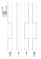
- FIG. 2 is an explanatory diagram (timing chart) illustrating the operation of an input circuit and the like.
- the present disclosure has been made in view of such circumstances, and its purpose is to provide an in-vehicle device equipped with an input circuit that can efficiently make judgments regarding input voltages. .
- an in-vehicle device including an input circuit that efficiently makes a determination regarding an input voltage.
- An in-vehicle device is an in-vehicle device that is mounted on a vehicle, and includes an input circuit including an input terminal into which an input voltage is input, and a drive that outputs a drive voltage to the input circuit.
- the input circuit includes a pnp bipolar transistor, a pull-up circuit, a second pull-up resistor, and a base resistor
- the pull-up circuit includes a pull-up power supply connected in series, a first pull-up and a second diode having an anode directed toward the first pull-up resistor, the second pull-up resistor is provided between the base of the pnp bipolar transistor and the input terminal, and the second pull-up resistor is connected to the pnp bipolar transistor.
- the base resistor is provided between the base of the pnp type bipolar transistor and the drive power supply circuit, and the base resistor is provided between the base of the pnp type bipolar transistor and the second pull-up resistor, and the base resistor is provided between the base of the pnp type bipolar transistor and the second pull-up resistor.
- a first diode is interposed between a connection point between the pull-up resistor and the base resistor and the input terminal, with its cathode facing the input terminal.
- the in-vehicle device includes an input circuit, a drive power supply circuit that outputs a drive voltage to the input circuit, and a voltage conversion circuit connected to the output end of the input circuit.
- These input circuits and drive power supply circuits constitute a low-side input circuit device.
- the vehicle-mounted device including the low-side input circuit device functions, for example, as a body ECU that controls the drive of body-related actuators mounted on the vehicle, a relay device such as a CAN gateway, or an electrical connection box including a semiconductor fuse.
- the in-vehicle device (low-side input circuit device) outputs a high or low signal (output voltage) in response to an input voltage input from an input end of an input circuit (a connector end to which an input connector is connected).
- a high or low signal (output voltage) is outputted to a microcomputer or the like from a voltage conversion circuit connected to an output end of an input circuit, for example.
- a microcomputer to which a high or low signal (output voltage) is input performs various control processing or calculation processing based on the signal (output voltage).
- the input circuit includes a pnp bipolar transistor, and a first conductive path extending from the input end (connector end) is connected to the base of the pnp bipolar transistor.
- the first conductive path is provided with a first diode and a base resistor, and in this case, the voltage at the input terminal (V: input terminal voltage) varies from the drive voltage (V_OUT) to the first diode.
- the emitter/base of a pnp bipolar transistor is The voltage drop between them is determined (Vbe ⁇ (Ri+Rb)/Ri).
- the error (variation) in the internal resistance (Ri) of the digital transistor is large, and the resistance voltage division ratio may change greatly.
- the input circuit uses a pnp type bipolar transistor, and by connecting the second pull-up resistor and the base resistor in parallel, resistor voltage division can be abolished (unnecessary), and a digital transistor can be used.
- the variation can be reduced compared to the case. Thereby, it is possible to realize high precision of the threshold value, and also to use a relatively inexpensive element, so that it is possible to reduce the product cost.
- the drive power supply circuit includes a drive power supply, an npn bipolar transistor, a first resistor, and a second resistor connected in series to the first resistor, and The drive voltage is output according to a resistance voltage division ratio between the first resistor and the second resistor.
- the drive power supply circuit includes a drive power supply, an npn type bipolar transistor, a first resistor, and a second resistor connected in series to the first resistor, and is configured by, for example, an emitter follower circuit.
- the drive power supply circuit uses the emitter follower circuit in this way, the first resistor (R1 ) and the resistance voltage division ratio using the second resistor (R2), the output voltage can be adjusted.
- the threshold value for determining low or high (ON/OFF voltage threshold
- the in-vehicle device further includes a voltage conversion circuit that performs voltage conversion between the input circuit and the microcomputer, and the voltage conversion circuit includes a level shift power supply and a digital transistor.
- the circuit outputs the voltage converted by the level shift circuit to the microcomputer connected to the collector of the digital transistor.
- the voltage conversion circuit is configured with a level shift circuit including a level shift power supply and a digital transistor, and the output voltage level-shifted (voltage converted) by the level shift circuit is output from the voltage conversion circuit. be done.
- the voltage conversion circuit performs voltage conversion between the input circuit and the microcomputer.
- an electronic component with a calculation function such as a microcomputer, IC (Integrated Circuit), ASIC (Application Specific Integrated Circuit), or FPGA (Field-Programmable Gate Array) is connected to the output end (microcomputer end) of the voltage conversion circuit.
- the threshold voltage of the microcomputer or the like may not correspond to the output voltage from the drive power supply circuit.
- the microcomputer etc. can be controlled without depending on the output voltage (pull-up voltage) from the drive power supply circuit. It can correspond to (satisfy) the threshold voltage.
- FIG. 1 is a schematic diagram illustrating an overview of an on-vehicle device 1 mounted on a vehicle C according to a first embodiment.
- FIG. 2 is a circuit diagram illustrating the configuration of the input circuit 2 and the like included in the in-vehicle device 1.
- the on-vehicle device 1 is mounted on a vehicle C, and includes an input circuit 2 and a drive power circuit 4 that outputs a drive voltage to the input circuit 2, and further includes a voltage conversion circuit 5 connected to the output end of the input circuit 2. It may be something.
- the in-vehicle device 1 may further include a microcomputer 6 connected to the voltage conversion circuit 5.
- the drive power supply circuit 4 and the input circuit 2 are connected through a second conductive path 102.
- the input circuit 2 and the voltage conversion circuit 5 are connected through a third conductive path 103.
- the input circuit 2, drive power supply circuit 4, and voltage conversion circuit 5 constitute a low-side input circuit device.
- the in-vehicle device 1 functioning as the low-side input circuit device outputs a signal (output voltage) indicating high (Hi) or low (Lo) to the microcomputer 6 according to the voltage value of the input voltage input to the input circuit 2. do.
- the input circuit 2 and the drive power supply circuit 4 determine a threshold value (threshold value of ON/OFF voltage) when determining whether the input voltage is high or low.
- the input circuit 2 is equipped with a pnp type bipolar transistor T2, and has a configuration that eliminates the voltage division ratio using the base resistor R5, etc., so it is possible to set a relatively low voltage threshold, and to improve the accuracy of the threshold. Variations can be reduced.
- the drive power supply circuit 4 includes a drive power supply 41, an npn bipolar transistor T1, a first resistor R1, and a second resistor R2.
- the drive power source 41 outputs a voltage (for example, 12V) supplied from a power supply device such as a lead battery or an alternator mounted on the vehicle C to a predetermined voltage (for example, 5V) that is stepped down using a regulator or the like. .
- An npn bipolar transistor T1 is connected to the drive power source 41, and a voltage output from the drive power source 41 is always applied to the npn bipolar transistor T1.
- the electric wire extending from the drive power source 41 to the npn bipolar transistor T1 is branched into two, and each of the two branched ends is connected to the collector and base of the npn bipolar transistor T1.
- a first resistor R1 is provided between the drive power source 41 and the base of the npn bipolar transistor T1.
- a second resistor R2 is interposed in the electric wire extending from the first resistor R1 to the ground. That is, an electric wire extending from the connection point between the first resistor R1 and the second resistor R2 is connected to the base of the npn type bipolar transistor T1.
- the first resistor R1 and the second resistor R2 are connected in series, and the base of the npn bipolar transistor T1 is connected to the connection point between the first resistor R1 and the second resistor R2.
- the voltage output from the emitter of the npn bipolar transistor T1 has a voltage value according to the resistance voltage division ratio of the first resistor R1 and the second resistor R2.
- the drive power supply circuit 4 has an emitter follower that steps down the output voltage (VCC) from the drive power supply 41 to a predetermined voltage (V_OUT) according to the resistance voltage division ratio of the first resistor R1 and the second resistor R2. Consists of circuits.
- the stepped down voltage corresponds to the output voltage (V_OUT) of the drive power supply circuit 4.
- the npn bipolar transistor T1 can be used in an analog manner based on the operating principle of a linear regulator, and the output voltage (V_OUT) can be adjusted by resistor voltage division. This eliminates the need for a relatively expensive comparator and makes it possible to realize (satisfy) the necessary functions with an inexpensive configuration.
- the output voltage (V_OUT) of the drive power supply circuit 4 is controlled by the resistance of the first resistor R1 ( ⁇ :R1) and the second resistor R2 ( ⁇ :R2) so that the output voltage (V_OUT) of the drive power supply circuit 4 is constant with respect to the output voltage (VCC) of the drive power supply 41.
- the resistance voltage division ratio can be changed by changing the resistance constants of the first resistor R1 and the second resistor R2. Therefore, the threshold value (ON/OFF voltage threshold) for determining high or low can be efficiently adjusted. Therefore, the availability of the drive power supply circuit 4 can be improved.
- the emitter of the npn bipolar transistor T1 and the emitter of the pnp bipolar transistor T2 included in the input circuit 2 are connected by a second conductive path 102.
- An output voltage (V_OUT) lowered by the resistance voltage division ratio from the drive power supply circuit 4 is always applied to the pnp bipolar transistor T2 of the input circuit 2.
- the input circuit 2 includes a pnp bipolar transistor T2, a second pull-up resistor R4, a base resistor R5, a pull-up circuit 3, and an input terminal 21.
- a second conductive path 102 is connected to the emitter of the pnp bipolar transistor T2, and an output voltage (V_OUT) that is stepped down from the drive power supply circuit 4 at a resistance voltage division ratio is transmitted through the second conductive path 102. , is always applied.
- the base of the pnp bipolar transistor T2 is connected to the input terminal 21 via a first conductive path 101.
- the input end 21 may be configured with a connector terminal or the like, for example, and may function as a connector end.
- An input voltage to be determined as high or low is input to the input end 21 (connector end).
- the collector of the pnp bipolar transistor T2 is connected to the voltage conversion circuit 5 through a third conductive path 103.
- the collector of the pnp bipolar transistor T2 corresponds to the output end of the input circuit.
- a second pull-up resistor R4 is provided between the second conductive path 102 and the first conductive path 101. That is, the second pull-up resistor R4 is connected to the first conductive path 101 at the second connection point S2, and connected to the second conductive path 102 at the third connection point S3.
- the base resistor R5 is provided interposed between the base of the pnp bipolar transistor T2 and the third connection point S3 (the connection point between the second pull-up resistor R4 and the first conductive path 101). With such a configuration, it is possible to eliminate resistive voltage division for the voltage (V: input terminal 21 voltage) of the input terminal 21 (connector terminal) connected to the base of the pnp type bipolar transistor T2. For example, when using a digital transistor T3 with a built-in resistor, the internal resistance and the base resistance R5 are connected in series, and due to variations in the internal resistance, the resistance voltage division ratio changes, and the voltage at the input terminal 21 (connector terminal) ( There is a concern that the voltage (V: input terminal 21 voltage) may vary.
- the resistor voltage division can be abolished and the input voltage can be easily judged as high or low.
- the accuracy of the threshold value can be improved.
- the pull-up circuit 3 includes a pull-up power supply 31, a first pull-up resistor R3, and a second diode D2.
- the pull-up power supply 31, the first pull-up resistor R3, and the second diode D2 are connected in series in this order in the direction of current flow from the pull-up power supply 31.
- the cathode of the second diode D2 and the first conductive path 101 are connected at the first connection point S1.
- a first diode D1 has an anode connected to the second connection point S2 side (base side of the pnp bipolar transistor T2). It is provided interposed towards the target.
- the potential of the first conductive path 101 is unstable. This can be prevented and the potential can be efficiently maintained at a sufficiently high potential that corresponds to the product specifications.
- the input circuit 2 configured in this way functions as a low-side input circuit.
- the threshold value (ON/OFF voltage threshold) for determining low or high for the input voltage (Vin) input from the input end 21 (connector end) is the voltage at the input end 21 (V: input end 21 voltage) It will be based on.
- the voltage at the input terminal 21 (V: input terminal 21 voltage) is calculated from the output voltage (V_OUT) from the drive power supply circuit 4, the voltage drop of the first diode D1 (VfD: forward voltage), and the voltage drop of the pnp bipolar transistor T2.
- the threshold value (ON/OFF voltage threshold) for determining high/low with respect to the input voltage (Vin) input to the input terminal 21 is a relatively small value (low voltage)
- the pnp type bipolar transistor The temperature characteristics of each element, such as T2 and the first diode D1, have an influence.
- the input voltage (Vin) is affected by the voltage drop of the first diode D1 and the voltage drop between the emitter and base of the pnp bipolar transistor T2
- variations can be reduced and the threshold value High precision can be achieved.
- the voltage conversion circuit 5 is configured with a level shift circuit including a level shift power supply 51 and a digital transistor T3.
- the digital transistor T3 is an npn type transistor equipped with an internal resistance.
- a third conductive path 103 extending from the collector of the pnp bipolar transistor T2 of the input circuit 2 is connected to the base of the digital transistor T3.
- the collector of the digital transistor T3 is connected to the microcomputer 6 and the level shift power supply 51.
- the emitter of the digital transistor T3 is grounded.
- the level shift power supply 51 and the level shift resistor R6 are connected in series, and the level shift resistor R6 is connected to an electric wire connecting the microcomputer 6 and the collector of the digital transistor T3. That is, one end of the level shift resistor R6 is connected to the level shift power supply 51, and the other end of the level shift resistor R6 is connected to an electric wire connecting the microcomputer 6 and the collector of the digital transistor T3.
- the digital transistor T3 is turned on or off depending on the voltage input through the third conductive path 103 connected to its base.
- a high (Hi) voltage is input from the level shift power supply 51 to the microcomputer 6.
- the digital transistor T3 is on, the microcomputer 6 has a ground potential, and a low voltage is input to the microcomputer 6.
- the threshold voltage of the microcomputer 6 etc. connected to the voltage conversion circuit 5 depends on the output voltage (V_OUT) from the drive power supply circuit 4. The threshold voltage can be satisfied without having to do so.
- the microcomputer 6 is a computer that has a control section such as an MPU, a storage section such as a RAM or ROM, an input/output terminal, etc., and is equipped with arithmetic functions.
- the microcomputer 6 determines whether the input voltage input from the input end 21 (connector end) is high (Hi) or low (Lo), depending on the output voltage output from the voltage conversion circuit 5. For example, a threshold voltage is set in the microcomputer 6, and when the output voltage output from the voltage conversion circuit 5 is equal to or higher than the threshold voltage, it is determined as high (Hi), and when it is less than the threshold voltage, it is determined as high (Hi). , a low determination may be made.
- An electronic component having an arithmetic function, such as an array), may be connected.
- FIG. 3 is an explanatory diagram (timing chart) illustrating the operation of the input circuit 2 and the like.
- the input terminal 21 connector terminal
- the npn type bipolar transistor T1 of the drive power supply circuit 4 the pnp type bipolar transistor T2 of the input circuit 2
- the digital transistor T3 microcomputer
- the operation at the 6th terminal will be explained in terms of voltage levels (Hi, Lo).
- the symbols A to D shown in FIG. 3 correspond to the symbols indicated by the arrows in FIG. 2, and each voltage level (Hi, Lo) is the voltage level (Hi, Lo) at the location indicated by the arrow. exemplify.
- the npn type bipolar transistor T1 of the drive power supply circuit 4 is always on, and as described above, the drive voltage stepped down according to the resistor voltage division ratio is transmitted to the pnp type bipolar transistor of the input circuit 2 via the first conductive path 101. Output (apply) to T2.
- the input end 21 (connector end) of the input circuit 2 changes depending on the input voltage that is input.
- the input voltage may vary from 12V to 0V, for example.
- the pnp type bipolar transistor T2 of the input circuit 2 When the voltage level of the input voltage at the input terminal 21 (connector terminal) of the input circuit 2 is high (Hi), the pnp type bipolar transistor T2 of the input circuit 2 is turned off, and the voltage is output from the collector of the pnp type bipolar transistor T2. The voltage level of the voltage becomes low (Lo). In this case, the digital transistor T3 of the voltage conversion circuit 5 is turned off, and the voltage level of the emitter of the digital transistor T3, that is, the voltage at the end of the microcomputer 6 to which the microcomputer 6 is connected becomes high (Hi).
- the pnp bipolar transistor T2 When the voltage level of the input voltage at the input end 21 (connector end) of the input circuit 2 is low, the pnp bipolar transistor T2 is turned on, and the voltage level of the voltage output from the collector of the pnp bipolar transistor T2 is becomes high (Hi). In this case, the digital transistor T3 of the voltage conversion circuit 5 is turned on, and the voltage level of the collector of the digital transistor T3, that is, the voltage at the end of the microcomputer 6 to which the microcomputer 6 is connected becomes low (Lo).
- the input circuit 2 (low-side input circuit), drive power supply circuit 4 (emitter follower circuit), and voltage conversion circuit 5 (level shift circuit) included in the on-vehicle device 1 are input to the input end 21 (connector end) as described above. Performs high/low judgment for input voltage. In this way, each of the input circuit 2 (low-side input circuit), drive power supply circuit 4 (emitter follower circuit), and voltage conversion circuit 5 (level shift circuit) is suitably configured, and by combining these, the input voltage Judgments can be made efficiently.
- the claims may include multiple dependent claims that are dependent on multiple claims. Multiple dependent claims may be written that are dependent on multiple dependent claims. Even if a multiple dependent claim that is dependent on a multiple dependent claim is not written, this does not limit the writing of the multiple dependent claim that is dependent on the multiple dependent claim.
Landscapes
- Engineering & Computer Science (AREA)
- Computer Hardware Design (AREA)
- Physics & Mathematics (AREA)
- Computing Systems (AREA)
- General Engineering & Computer Science (AREA)
- Mathematical Physics (AREA)
- Logic Circuits (AREA)
- Semiconductor Integrated Circuits (AREA)
Abstract
Description
本出願は、2022年7月6日出願の日本出願第2022-109144号に基づく優先権を主張し、前記日本出願に記載された全ての記載内容を援用するものである。
特許文献1に記載のトランジスタを用いた定電流駆動装置においては、入力された電圧に対し所定の閾値に基づきハイ又はローであるかを判定するにあたり、当該閾値が小さい場合であっても、当該判定を効率的に行う点については、考慮されていない。
本開示の一態様によれば、入力された電圧に対する判定を効率的に行う入力回路を備える車載装置を提供することができる。
最初に本開示の実施態様を列挙して説明する。また、以下に記載する実施形態の少なくとも一部を任意に組み合わせてもよい。
本開示をその実施の形態を示す図面に基づいて具体的に説明する。本開示の実施形態に係る車載装置1を、以下に図面を参照しつつ説明する。なお、本開示はこれらの例示に限定されるものではなく、請求の範囲によって示され、請求の範囲と均等の意味及び範囲内での全ての変更が含まれることが意図される。
以下、実施の形態について図面に基づいて説明する。図1は、実施形態1に係る車両Cに搭載される車載装置1の概要を例示する模式図である。図2は、車載装置1に含まれる入力回路2等の構成を例示する回路図である。車載装置1は、車両Cに搭載され、入力回路2、及び入力回路2への駆動電圧を出力する駆動電源回路4を備え、更に入力回路2の出力端に接続される電圧変換回路5を備えるものであってもよい。車載装置1は、更に当該電圧変換回路5に接続されるマイコン6を備えるものであってもよい。駆動電源回路4と入力回路2とは、第2導電路102にて接続されている。入力回路2と電圧変換回路5とは、第3導電路103にて接続されている。
1 車載装置
101 第1導電路
102 第2導電路
103 第3導電路
2 入力回路(ローサイド入力回路)
21 入力端(コネクタ端)
T2 pnp型バイポーラトランジスタ
R4 第2プルアップ抵抗
S2 第2接続点
S3 第3接続点
R5 ベース抵抗
3 プルアップ回路
31 プルアップ電源
R3 第1プルアップ抵抗
D2 第2ダイオード
S1 第1接続点
D1 第1ダイオード
4 駆動電源回路(エミッタフォロワー回路)
41 駆動電源
T1 npn型バイポーラトランジスタ
R1 第1抵抗
R2 第2抵抗
5 電圧変換回路(レベルシフト回路)
51 レベルシフト電源
T3 デジタルトランジスタ
R6 レベルシフト用抵抗
6 マイコン
Claims (3)
- 車両に搭載される車載装置であって、
入力電圧が入力される入力端を含む入力回路と、
前記入力回路への駆動電圧を出力する駆動電源回路とを備え、
前記入力回路は、pnp型バイポーラトランジスタ、プルアップ回路、第2プルアップ抵抗、及びベース抵抗を含み、
前記プルアップ回路は、直列に接続されるプルアップ電源、第1プルアップ抵抗及び、前記第1プルアップ抵抗にアノードを向けた第2ダイオードを含み、前記pnp型バイポーラトランジスタのベースと、前記入力端との間に設けられ、
前記第2プルアップ抵抗は、前記pnp型バイポーラトランジスタのベースと、前記駆動電源回路との間に設けられ、
前記ベース抵抗は、前記pnp型バイポーラトランジスタのベースと、前記第2プルアップ抵抗との間に設けられており、
前記第2プルアップ抵抗と前記ベース抵抗との接続点と、前記入力端との間には、第1ダイオードがカソードを前記入力端に向けて介在している
車載装置。 - 前記駆動電源回路は、
駆動電源、npn型バイポーラトランジスタ、第1抵抗、及び、第1抵抗に直列に接続される第2抵抗を含み、
前記第1抵抗と前記第2抵抗とによる抵抗分圧比に応じた前記駆動電圧を出力する
請求項1に記載の車載装置。 - 前記入力回路とマイコン間にて電圧変換を行う電圧変換回路を更に備え、
前記電圧変換回路は、
レベルシフト電源とデジタルトランジスタとを含むレベルシフト回路であり、
前記レベルシフト回路にて変換された電圧を、前記デジタルトランジスタのコレクタに接続される前記マイコンに出力する
請求項1又は請求項2に記載の車載装置。
Priority Applications (2)
| Application Number | Priority Date | Filing Date | Title |
|---|---|---|---|
| CN202380048206.9A CN119325690A (zh) | 2022-07-06 | 2023-06-20 | 车载装置 |
| US18/880,639 US20260012181A1 (en) | 2022-07-06 | 2023-06-20 | On-board device |
Applications Claiming Priority (2)
| Application Number | Priority Date | Filing Date | Title |
|---|---|---|---|
| JP2022109144A JP7779210B2 (ja) | 2022-07-06 | 2022-07-06 | 車載装置 |
| JP2022-109144 | 2022-07-06 |
Publications (1)
| Publication Number | Publication Date |
|---|---|
| WO2024009758A1 true WO2024009758A1 (ja) | 2024-01-11 |
Family
ID=89453252
Family Applications (1)
| Application Number | Title | Priority Date | Filing Date |
|---|---|---|---|
| PCT/JP2023/022788 Ceased WO2024009758A1 (ja) | 2022-07-06 | 2023-06-20 | 車載装置 |
Country Status (4)
| Country | Link |
|---|---|
| US (1) | US20260012181A1 (ja) |
| JP (1) | JP7779210B2 (ja) |
| CN (1) | CN119325690A (ja) |
| WO (1) | WO2024009758A1 (ja) |
Citations (3)
| Publication number | Priority date | Publication date | Assignee | Title |
|---|---|---|---|---|
| JPS552237U (ja) * | 1978-06-21 | 1980-01-09 | ||
| JPH03184409A (ja) * | 1989-12-13 | 1991-08-12 | Nissan Motor Co Ltd | 半導体フィルタ回路 |
| JP2009117946A (ja) * | 2007-11-02 | 2009-05-28 | Toyota Motor Corp | 入力回路付き電子部品回路 |
-
2022
- 2022-07-06 JP JP2022109144A patent/JP7779210B2/ja active Active
-
2023
- 2023-06-20 CN CN202380048206.9A patent/CN119325690A/zh active Pending
- 2023-06-20 WO PCT/JP2023/022788 patent/WO2024009758A1/ja not_active Ceased
- 2023-06-20 US US18/880,639 patent/US20260012181A1/en active Pending
Patent Citations (3)
| Publication number | Priority date | Publication date | Assignee | Title |
|---|---|---|---|---|
| JPS552237U (ja) * | 1978-06-21 | 1980-01-09 | ||
| JPH03184409A (ja) * | 1989-12-13 | 1991-08-12 | Nissan Motor Co Ltd | 半導体フィルタ回路 |
| JP2009117946A (ja) * | 2007-11-02 | 2009-05-28 | Toyota Motor Corp | 入力回路付き電子部品回路 |
Also Published As
| Publication number | Publication date |
|---|---|
| JP2024007809A (ja) | 2024-01-19 |
| CN119325690A (zh) | 2025-01-17 |
| JP7779210B2 (ja) | 2025-12-03 |
| US20260012181A1 (en) | 2026-01-08 |
Similar Documents
| Publication | Publication Date | Title |
|---|---|---|
| US20040008070A1 (en) | Clamp circuit | |
| EP0493750A2 (en) | A comparator circuit with precision hysteresis and high input impedance | |
| CN105306018B (zh) | 施密特触发器电路和电源监视装置 | |
| JP3840319B2 (ja) | 電力線利用の電流通信回路 | |
| JP5130835B2 (ja) | 差動増幅回路とそれを用いた電流制御装置 | |
| CN110649791B (zh) | 电流检测电路及电源装置 | |
| WO2024009758A1 (ja) | 車載装置 | |
| US11378598B2 (en) | Semiconductor integrated circuit device and current detection circuit | |
| JP3829765B2 (ja) | 電源回路 | |
| US7471119B2 (en) | Electronic circuit device | |
| JP2010135981A (ja) | レベルシフト回路 | |
| JP2006288049A (ja) | 負荷制御回路、電流制御回路、及び、負荷制御システム | |
| US20250309884A1 (en) | Switch device, load drive system, and switch system | |
| JP4781320B2 (ja) | 定電圧回路、電子機器、電子制御機器 | |
| US12346287B2 (en) | Device for automatically detecting coupling between electronic devices | |
| JP2014204598A (ja) | 電子制御装置 | |
| CN112313489A (zh) | 车载用的温度检测电路 | |
| JP2008228266A (ja) | 半導体集積回路装置およびスイッチ入力回路 | |
| US11171585B2 (en) | Motor controller | |
| JP2010132070A (ja) | 自動車用電装機器 | |
| JP4461827B2 (ja) | 電源回路 | |
| JP2019203693A (ja) | 電子制御装置 | |
| KR100618536B1 (ko) | 차량 이씨유의 감압 레귤레이터 회로 | |
| JPH04812A (ja) | 電子回路 | |
| JP2002091582A (ja) | 定電圧電源回路 |
Legal Events
| Date | Code | Title | Description |
|---|---|---|---|
| 121 | Ep: the epo has been informed by wipo that ep was designated in this application |
Ref document number: 23835292 Country of ref document: EP Kind code of ref document: A1 |
|
| WWE | Wipo information: entry into national phase |
Ref document number: 202380048206.9 Country of ref document: CN |
|
| WWE | Wipo information: entry into national phase |
Ref document number: 18880639 Country of ref document: US |
|
| WWP | Wipo information: published in national office |
Ref document number: 202380048206.9 Country of ref document: CN |
|
| NENP | Non-entry into the national phase |
Ref country code: DE |
|
| 122 | Ep: pct application non-entry in european phase |
Ref document number: 23835292 Country of ref document: EP Kind code of ref document: A1 |
|
| WWP | Wipo information: published in national office |
Ref document number: 18880639 Country of ref document: US |