WO2024009727A1 - センサ及び把持負荷検出デバイス - Google Patents
センサ及び把持負荷検出デバイス Download PDFInfo
- Publication number
- WO2024009727A1 WO2024009727A1 PCT/JP2023/022323 JP2023022323W WO2024009727A1 WO 2024009727 A1 WO2024009727 A1 WO 2024009727A1 JP 2023022323 W JP2023022323 W JP 2023022323W WO 2024009727 A1 WO2024009727 A1 WO 2024009727A1
- Authority
- WO
- WIPO (PCT)
- Prior art keywords
- viewed
- electrode
- sensor
- axis direction
- main surface
- Prior art date
- Legal status (The legal status is an assumption and is not a legal conclusion. Google has not performed a legal analysis and makes no representation as to the accuracy of the status listed.)
- Ceased
Links
Images









Classifications
-
- G—PHYSICS
- G01—MEASURING; TESTING
- G01B—MEASURING LENGTH, THICKNESS OR SIMILAR LINEAR DIMENSIONS; MEASURING ANGLES; MEASURING AREAS; MEASURING IRREGULARITIES OF SURFACES OR CONTOURS
- G01B7/00—Measuring arrangements characterised by the use of electric or magnetic techniques
- G01B7/16—Measuring arrangements characterised by the use of electric or magnetic techniques for measuring the deformation in a solid, e.g. by resistance strain gauge
-
- G—PHYSICS
- G01—MEASURING; TESTING
- G01L—MEASURING FORCE, STRESS, TORQUE, WORK, MECHANICAL POWER, MECHANICAL EFFICIENCY, OR FLUID PRESSURE
- G01L1/00—Measuring force or stress, in general
- G01L1/16—Measuring force or stress, in general using properties of piezoelectric devices
-
- H—ELECTRICITY
- H10—SEMICONDUCTOR DEVICES; ELECTRIC SOLID-STATE DEVICES NOT OTHERWISE PROVIDED FOR
- H10N—ELECTRIC SOLID-STATE DEVICES NOT OTHERWISE PROVIDED FOR
- H10N30/00—Piezoelectric or electrostrictive devices
- H10N30/01—Manufacture or treatment
- H10N30/06—Forming electrodes or interconnections, e.g. leads or terminals
- H10N30/063—Forming interconnections, e.g. connection electrodes of multilayered piezoelectric or electrostrictive parts
-
- H—ELECTRICITY
- H10—SEMICONDUCTOR DEVICES; ELECTRIC SOLID-STATE DEVICES NOT OTHERWISE PROVIDED FOR
- H10N—ELECTRIC SOLID-STATE DEVICES NOT OTHERWISE PROVIDED FOR
- H10N30/00—Piezoelectric or electrostrictive devices
- H10N30/30—Piezoelectric or electrostrictive devices with mechanical input and electrical output, e.g. functioning as generators or sensors
-
- H—ELECTRICITY
- H10—SEMICONDUCTOR DEVICES; ELECTRIC SOLID-STATE DEVICES NOT OTHERWISE PROVIDED FOR
- H10N—ELECTRIC SOLID-STATE DEVICES NOT OTHERWISE PROVIDED FOR
- H10N30/00—Piezoelectric or electrostrictive devices
- H10N30/30—Piezoelectric or electrostrictive devices with mechanical input and electrical output, e.g. functioning as generators or sensors
- H10N30/302—Sensors
-
- H—ELECTRICITY
- H10—SEMICONDUCTOR DEVICES; ELECTRIC SOLID-STATE DEVICES NOT OTHERWISE PROVIDED FOR
- H10N—ELECTRIC SOLID-STATE DEVICES NOT OTHERWISE PROVIDED FOR
- H10N30/00—Piezoelectric or electrostrictive devices
- H10N30/80—Constructional details
- H10N30/85—Piezoelectric or electrostrictive active materials
- H10N30/857—Macromolecular compositions
-
- H—ELECTRICITY
- H10—SEMICONDUCTOR DEVICES; ELECTRIC SOLID-STATE DEVICES NOT OTHERWISE PROVIDED FOR
- H10N—ELECTRIC SOLID-STATE DEVICES NOT OTHERWISE PROVIDED FOR
- H10N30/00—Piezoelectric or electrostrictive devices
- H10N30/80—Constructional details
- H10N30/87—Electrodes or interconnections, e.g. leads or terminals
-
- H—ELECTRICITY
- H10—SEMICONDUCTOR DEVICES; ELECTRIC SOLID-STATE DEVICES NOT OTHERWISE PROVIDED FOR
- H10N—ELECTRIC SOLID-STATE DEVICES NOT OTHERWISE PROVIDED FOR
- H10N30/00—Piezoelectric or electrostrictive devices
- H10N30/80—Constructional details
- H10N30/87—Electrodes or interconnections, e.g. leads or terminals
- H10N30/875—Further connection or lead arrangements, e.g. flexible wiring boards, terminal pins
Definitions
- the present invention relates to a sensor and a grip load detection device including the sensor.
- a piezoelectric film sensor described in Patent Document 1 As an invention related to a conventional sensor, for example, a piezoelectric film sensor described in Patent Document 1 is known.
- the piezoelectric film sensor described in Patent Document 1 includes a sensor section, a circuit section, and a holding member.
- the sensor section outputs a piezoelectric voltage according to the amount of distortion of the piezoelectric film from the output conductor pattern.
- the circuit section includes an input conductor pattern into which the piezoelectric voltage output from the output conductor pattern is input.
- the holding member holds the sensor section and the circuit section in a state where the output conductor pattern and the input conductor pattern are electrically connected.
- an object of the present invention is to provide a sensor that can reduce the area of a portion where an output conductor of a sensor section and an input conductor of a circuit section are connected when viewed in the normal direction of the main surface of the sensor section.
- An object of the present invention is to provide a grip load detection device.
- a sensor includes: a piezoelectric film having a first main surface and a second main surface facing each other in a first direction; a first electrode provided on the first main surface; a second electrode provided on the second main surface; It is equipped with a wiring section and The first electrode and the second electrode overlap each other and include a first portion that overlaps the piezoelectric film when viewed in the first direction, The first electrode and the second electrode include second portions that overlap each other and do not overlap the piezoelectric film when viewed in the first direction, the first portion and the second portion are arranged in a second direction perpendicular to the first direction,
- the wiring section is a wiring board that is an insulator and has a third main surface and a fourth main surface that overlap the second portion and face the first direction when viewed in the first direction; a first conductor provided on the third main surface and electrically connected to the first electrode; a second conductor provided on the fourth main surface and electrically connected to the second electrode.
- the sensor according to the present invention it is possible to reduce the connection area between the output conductor of the sensor section and the input conductor of the circuit section when viewed in the normal direction of the main surface of the sensor section.
- FIG. 1 is a plan view of a sensor 100 according to the first embodiment viewed in the Z-direction.
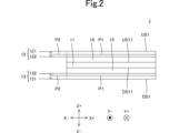
- FIG. 2 is a cross-sectional view of the sensor section 1 according to the first embodiment, viewed in the Y+ direction.
- FIG. 3 is a plan view of the piezoelectric film 11 according to the first embodiment viewed in the Z-direction.
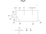
- FIG. 4 is a plan view of the sensor unit 1 according to the first embodiment viewed in the Z-direction.
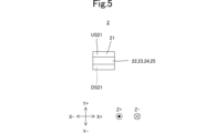
- FIG. 5 is a plan view of the wiring section 2 according to the first embodiment viewed in the Z-direction.
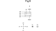
- FIG. 6 is a cross-sectional view of the wiring section 2 according to the first embodiment, viewed in the Y+ direction.
- FIG. 1 is a plan view of a sensor 100 according to the first embodiment viewed in the Z-direction.
- FIG. 2 is a cross-sectional view of the sensor section 1 according to the first embodiment, viewed in the Y+ direction.
- FIG. 3 is a plan
- FIG. 7 is a cross-sectional view taken along line AA of the sensor 100 according to the first embodiment.
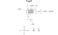
- FIG. 8 is a plan view of the wiring portion 2 and the second portion P2 according to the first embodiment as viewed in the Z-direction.
- FIG. 9 is a plan view of a sensor 1000 according to a comparative example viewed in the Z-direction.
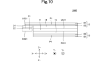
- FIG. 10 is a sectional view taken along line BB of a sensor 1000 according to a comparative example.
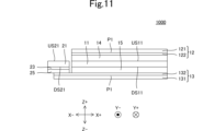
- FIG. 11 is a sectional view taken along line CC of a sensor 1000 according to a comparative example.
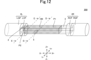
- FIG. 12 is a perspective view of the grip load detection device 200 according to the first embodiment.
- FIG. 13 is a sectional view taken along line DD of the grip load detection device 200 according to the first embodiment.
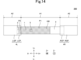
- FIG. 14 is a plan view of the grip load detection device 200 according to the first embodiment, viewed in the Z-direction.
- FIG. 15 is a sectional view taken along line EE of the gripping load detection device 200 according to the first embodiment.
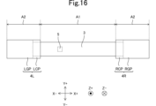
- FIG. 16 is a plan view of the transparent housing 3, the first grip 4L, the second grip 4R, and the light emitter 5 according to the first embodiment, as viewed in the Z-direction.
- FIG. 17 is a diagram showing a transparent area ATP and a non-transparent area ANTP of the sensor section 1 according to the first embodiment.
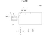
- FIG. 18 is a plan view of the sensor 100a according to the first modification as viewed in the Z-direction.
- FIG. 19 is a plan view of the sensor unit 1 according to the first modification as viewed in the Z-direction.
- FIG. 20 is a perspective view of a gripping load detection device 200a according to a first modification.
- FIG. 21 is a diagram showing the transparent area ATP and non-transparent area ANTP of the sensor 100a according to the first modification.
- FIG. 22 is a plan view of a sensor 100b according to a second modification as viewed in the Z-direction.
- FIG. 23 is a perspective view of a grip load detection device 200b according to a second modification.
- FIG. 24 is a plan view of a gripping load detection device 200b according to a second modification as viewed in the Z-direction.
- FIG. 1 is a plan view of a sensor 100 according to the first embodiment viewed in the Z-direction.
- FIG. 2 is a cross-sectional view of the sensor section 1 according to the first embodiment, viewed in the Y+ direction.
- FIG. 3 is a plan view of the piezoelectric film 11 according to the first embodiment viewed in the Z-direction.
- FIG. 4 is a plan view of the sensor unit 1 according to the first embodiment viewed in the Z-direction.
- FIG. 5 is a plan view of the wiring section 2 according to the first embodiment viewed in the Z-direction.
- FIG. 1 is a plan view of a sensor 100 according to the first embodiment viewed in the Z-direction.
- FIG. 2 is a cross-sectional view of the sensor section 1 according to the first embodiment, viewed in the Y+ direction.
- FIG. 3 is a plan view of the piezoelectric film 11 according to the first embodiment viewed in the Z-direction.
- FIG. 4 is a plan view
- FIG. 6 is a cross-sectional view of the wiring section 2 according to the first embodiment, viewed in the Y+ direction.
- FIG. 7 is a cross-sectional view taken along line AA of the sensor 100 according to the first embodiment.
- FIG. 8 is a plan view of the wiring portion 2 and the second portion P2 according to the first embodiment as viewed in the Z-direction.
- FIG. 9 is a plan view of a sensor 1000 according to a comparative example viewed in the Z-direction.
- FIG. 10 is a sectional view taken along line BB of a sensor 1000 according to a comparative example.
- FIG. 11 is a sectional view taken along line CC of a sensor 1000 according to a comparative example.
- the X-axis direction, the Y-axis direction, and the Z-axis direction are orthogonal to each other.
- the Z-axis direction corresponds to the "first direction” of the present invention.
- the X-axis direction corresponds to the "second direction” of the present invention.
- the Y-axis direction corresponds to the "third direction” of the present invention.
- the X+ direction is the positive direction of the X axis.
- the X-direction is the negative direction of the X-axis.
- the Y+ direction is the positive direction of the Y axis.
- the Y-direction is the negative direction of the Y-axis.
- the Z+ direction is the positive direction of the Z axis.
- the Z-direction is the negative direction of the Z-axis.
- the Z-axis direction is an example of the "first direction” of the present invention.
- the X-axis direction is an example of the "second direction” of the present invention.
- the Y-axis direction is an example of the "third direction” of the present invention.
- the object 10 is transparent means that when the object 10 is viewed from the Y- direction, the inside of the object 10 and the Y+ direction can be seen through the object 10. means. This definition also applies when the object 10 is viewed from a direction other than the Y-direction. This definition also applies to objects and regions other than the object 10.
- the sensor 100 is a sensor that detects deformation of the object to be measured.
- the sensor 100 includes a sensor section 1 and a wiring section 2, as shown in FIG.
- the sensor section 1 includes a piezoelectric film 11, a first electrode 12, a second electrode 13, a first adhesive material 14, and a second adhesive material 15, as shown in FIG.
- the sensor section 1 has a first main surface US1 and a second main surface DS1.
- the first main surface US1 and the second main surface DS1 face each other in the Z-axis direction.
- the first main surface US1 is located in the Z+ direction from the second main surface DS1.
- the first main surface US1 and the second main surface DS1 are parallel to each other.
- the piezoelectric film 11 has a third main surface US11 and a fourth main surface DS11.
- the third main surface US11 and the fourth main surface DS11 face each other in the Z-axis direction.
- the third main surface US11 corresponds to the "first main surface” of the present invention.
- the fourth principal surface DS11 corresponds to the "second principal surface” of the present invention.
- the third main surface US11 is located in the Z+ direction from the fourth main surface DS11.
- the third main surface US11 and the fourth main surface DS11 are parallel to each other.
- Each of the third main surface US11 and the fourth main surface DS11 has a rectangular shape when viewed in the Z-axis direction.
- Each of the third main surface US11 and the fourth main surface DS11 has a long side extending in the X-axis direction and a short side extending in the Y-axis direction.
- the piezoelectric film 11 is transparent. Moreover, the piezoelectric film 11 has high flexibility. Furthermore, the piezoelectric film 11 generates electric charges according to the amount of deformation of the piezoelectric film 11. In this embodiment, the piezoelectric film 11 is a PLLA film. Below, the piezoelectric film 11 will be explained in more detail.
- the piezoelectric film 11 is a film formed from a chiral polymer.
- the chiral polymer is, for example, polylactic acid (PLA), particularly L-type polylactic acid (PLLA).
- PLLA which is a chiral polymer, has a main chain having a helical structure.
- PLLA has piezoelectricity in which molecules are oriented by being uniaxially stretched.
- the piezoelectric film 11 has a piezoelectric constant of d14.
- the uniaxial stretching direction (orientation direction) OD of the piezoelectric film 11 forms an angle of 0 degrees with respect to the X-axis direction. This 0 degree includes, for example, an angle including approximately 0 degrees ⁇ 10 degrees.
- the piezoelectric film 11 is stretched in a direction of 45 degrees with respect to the X-axis direction and the Y-axis direction, and electric charges are generated. The magnitude of the charge depends on the amount of twist of the piezoelectric film 11.
- the first electrode 12 is a ground electrode.
- the first electrode 12 is electrically connected to ground potential. More specifically, the first electrode 12 has a first base material 121 and a first conductive film 122, as shown in FIG.
- the first conductive film 122 covers the end face of the first base material 121 in the Z-direction.
- the first conductive film 122 is electrically connected to the ground potential.
- the first electrode 12 is transparent. Further, the first electrode 12 has high flexibility.
- the first base material 121 is, for example, a PET (polyethylene terephthalate) film.
- the first conductive film 122 is, for example, a transparent conductive film.
- the material of the first conductive film 122 is, for example, ITO (indium tin oxide).
- the first electrode 12 is provided on the third main surface US11. More specifically, as shown in FIG. 2, the first electrode 12 is provided in the Z+ direction from the first adhesive material 14 provided on the third main surface US11. The first electrode 12 is fixed in the Z+ direction from the third main surface US11 by a first adhesive material 14. The first electrode 12 covers the end surface of the first adhesive material 14 in the Z+ direction. The first conductive film 122 is located between the first base material 121 and the first adhesive material 14. Further, the first main surface US1 of the sensor 100 is an end surface of the first electrode 12 in the Z+ direction.
- the first adhesive material 14 is transparent.
- the first adhesive material 14 is, for example, an optical transparent adhesive sheet.
- the first adhesive material 14 fixes the first conductive film 122 in the Z+ direction from the third main surface US11.
- the second electrode 13 is a signal electrode.
- the second electrode 13 outputs a deformation detection signal SigD according to the deformation of the piezoelectric film 11. More specifically, the second electrode 13 has a second base material 131 and a second conductive film 132, as shown in FIG.
- the second conductive film 132 covers the end surface of the second base material 131 in the Z+ direction.
- the second conductive film 132 outputs a deformation detection signal SigD according to the deformation of the piezoelectric film 11.
- the second electrode 13 is transparent. Further, the second electrode 13 has high flexibility.
- the second base material 131 is, for example, a PET (polyethylene terephthalate) film.
- the second conductive film 132 is, for example, a transparent conductive film.
- the material of the second conductive film 132 is, for example, ITO (indium tin oxide).
- the second electrode 13 is provided on the fourth main surface DS11. More specifically, as shown in FIG. 2, the second electrode 13 is provided in the Z-direction from the second adhesive material 15 provided on the fourth principal surface DS11. The second electrode 13 is fixed in the Z-direction from the fourth main surface DS11 by a second adhesive material 15. The second electrode 13 covers the end surface of the second adhesive material 15 in the Z-direction.
- the second conductive film 132 is located between the second base material 131 and the second adhesive material 15. Further, the second main surface DS1 of the sensor 100 is an end surface of the second electrode 13 in the Z-direction.
- the second adhesive material 15 is transparent.
- the second adhesive material 15 is, for example, an optical transparent adhesive sheet.
- the second adhesive material 15 fixes the second conductive film 132 in the Z-direction from the fourth principal surface DS11.
- the first electrode 12 and the second electrode 13 overlap each other when viewed in the Z-axis direction, as shown in FIGS. 2 and 4. Further, each of the first electrode 12 and the second electrode 13 has a first portion P1 that overlaps with the piezoelectric film 11. Therefore, the first portion P1 is transparent. Further, the first electrode 12 and the second electrode 13 overlap each other when viewed in the Z-axis direction. Further, each of the first electrode 12 and the second electrode 13 has a second portion P2 that does not overlap with the piezoelectric film 11. Therefore, the second portion P2 is transparent.
- the outer edge of the first portion P1 coincides with the outer edge of the piezoelectric film 11 when viewed in the Z-axis direction. More specifically, as shown in FIG. 4, the first portion P1 has a rectangular shape when viewed in the Z-axis direction. Moreover, the first portion P1 has a long side extending in the X-axis direction and a short side extending in the Y-axis direction when viewed in the Z-axis direction. That is, when viewed in the Z-axis direction, the first portion P1 has a first side SI1 and a second side SI2 extending in the X-axis direction, and a third side SI3 and a fourth side SI4 extending in the Y-axis direction. have.
- the first side SI1 is located further in the Y+ direction than the second side SI2. Further, the third side SI3 is located further in the Y-direction than the fourth side SI4. Therefore, the first portion P1 includes a first side SI1, which is a first end in the Y+ direction, and a second side SI2, which is a second end in the Y-direction.
- the second portion P2 has a rectangular shape when viewed in the Z-axis direction. Further, the second portion P2 has a long side extending in the X-axis direction and a short side extending in the Y-axis direction when viewed in the Z-axis direction. That is, when viewed in the Z-axis direction, the second portion P2 has a fifth side SI5 and a sixth side SI6 extending in the X-axis direction, and a seventh side SI7 and an eighth side SI8 extending in the Y-axis direction. have. Therefore, the second portion P2 includes the fifth side SI5, which is the third end in the Y+ direction, and also includes the sixth side SI6, which is the fourth end in the Y-direction.
- the first portion P1 and the second portion P2 are lined up in the X-axis direction, as shown in FIG. 4. Further, the length of the second portion P2 in the Y-axis direction is shorter than the length of the first portion P1 in the Y-axis direction.
- the first side SI1 of the first portion P1 is located in the Y+ direction from the fifth side SI5 of the second portion P2 when viewed in the Z-axis direction. That is, the first end of the first portion P1 is located in the Y+ direction from the third end of the second portion P2 when viewed in the Z-axis direction.
- the second side SI2 of the first portion P1 is located further in the Y-direction than the sixth side SI6 of the second portion P2 when viewed in the Z-axis direction. That is, the second end of the first portion P1 is located further in the Y-direction than the fourth end of the second portion P2 when viewed in the Z-axis direction.
- the wiring section 2 includes a wiring board 21, a first conductor 22, a second conductor 23, a first conductive adhesive 24, and a second conductive adhesive 25.
- first conductive adhesive material 24 is an example of the "first conductive adhesive” of the present invention.
- second conductive adhesive material 25 is an example of the "second conductive adhesive” of the present invention.
- the wiring board 21 overlaps the second portion P2 when viewed in the Z-axis direction. Further, as shown in FIG. 5, the wiring board 21 has a fifth main surface US21 and a sixth main surface DS21 that face each other in the Z-axis direction.
- the fifth principal surface US21 corresponds to the "third principal surface” of the present invention.
- the sixth principal surface DS21 corresponds to the "fourth principal surface” of the present invention.
- the fifth main surface US21 is located in the Z+ direction from the sixth main surface DS21.
- the fifth principal surface US21 and the sixth principal surface DS21 are parallel to each other.
- Each of the fifth principal surface US21 and the sixth principal surface DS21 has a rectangular shape when viewed in the Z-axis direction.
- Each of the fifth main surface US21 and the sixth main surface DS21 has a long side extending in the X-axis direction and a short side extending in the Y-axis direction.
- the wiring board 21 is a flexible board having flexibility. Moreover, the wiring board 21 is an insulator.
- the first conductor 22 is a ground line.
- the first conductor 22 is electrically connected to ground potential.
- the first conductor 22 is provided on the fifth main surface US21, as shown in FIG.
- the second conductor 23 is a signal line.
- the second conductor 23 is electrically connected to an input terminal of an arithmetic circuit (not shown).
- the second conductor 23 is provided on the sixth main surface DS21, as shown in FIG.
- the first conductive adhesive material 24 has conductivity. Furthermore, as shown in FIG. 1, the first conductive adhesive material 24 overlaps the second portion P2 when viewed in the Z-axis direction. Further, the first conductive adhesive material 24 is provided on the end surface of the first conductor 22 in the Z+ direction, as shown in FIG. The first conductive adhesive material 24 fixes the first electrode 12 in the Z+ direction from the end surface of the first conductor 22 in the Z+ direction. Thereby, the first conductor 22 is electrically connected to the first electrode 12 via the first conductive adhesive material 24.
- the second conductive adhesive material 25 has conductivity. Furthermore, as shown in FIG. 1, the second conductive adhesive material 25 overlaps the second portion P2 when viewed in the Z-axis direction. Further, the second conductive adhesive material 25 is provided on the end face of the second conductor 23 in the Z-direction, as shown in FIG. The second conductive adhesive material 25 fixes the second electrode 13 in the Z-direction from the end surface of the second conductor 23 in the Z-direction. Thereby, the second conductor 23 is electrically connected to the second electrode 13 via the second conductive adhesive material 25.
- the first electrode 12, first conductive adhesive 24, first conductor 22, wiring board 21, second conductor 23, second conductive adhesive 25, and second electrode 13 are In the third portion P3, which overlaps the second portion P2 when viewed in the direction, they are arranged in this order along the Z-axis direction. Therefore, the first electrode 12, the first conductive adhesive material 24, the wiring board 21, the second conductive adhesive material 25, and the second electrode 13 are located in the third portion P3 that overlaps with the second portion P2 when viewed in the Z-axis direction. , are lined up in this order along the Z-axis direction. Note that a portion of the third portion P3 coincides with a portion of the second portion P2.
- the third part P3 corresponds to the "fifth part" of the present invention.
- first position PO1 when viewed in the Z-axis direction, the position in the X-axis direction where the third portion P3 exists is defined as a first position PO1, as shown in FIG. Note that the first position PO1 may be any position in the X-axis direction where the third portion P3 is located.
- the length L21 of the wiring board 21 in the Y-axis direction at the first position PO1 is longer than the length LP2 of the second portion P2 in the Y-axis direction at the first position PO1.
- the length L24 of the first conductive adhesive material 24 in the Y-axis direction at the first position PO1 is shorter than the length LP2 of the second portion P2 in the Y-axis direction at the first position PO1.
- the length L25 of the second conductive adhesive material 25 in the Y-axis direction at the first position PO1 is shorter than the length LP2 of the second portion P2 in the Y-axis direction at the first position PO1.
- the connection area between the output conductor of the sensor section 1 and the input conductor of the circuit section when viewed in the normal direction of the main surface of the sensor section 1 can be reduced.
- a sensor 1000 according to a comparative example will be described. Note that regarding the sensor 1000 according to the comparative example, only the parts that are different from the sensor 100 according to the first embodiment will be explained, and the rest will be omitted.
- the first electrode 12 and the second electrode 13 do not have the second portion P2. More specifically, the first electrode 12 and the second electrode 13 are located at the end of the sensor unit 1 in the X-direction (the end of the sensor unit 1 in the They don't overlap.
- the first electrode 12 is located at the end of the sensor section 1 in the X-direction, at the half of the sensor section 1 in the Y+ direction when viewed in the Z-axis direction.
- the second electrode 13 is located at the end of the sensor section 1 in the X-direction, at a half of the sensor section 1 in the Y-direction when viewed in the Z-axis direction. That is, the first electrode 12 and the second electrode 13 are aligned in the Y-axis direction when viewed in the Z-axis direction at the end of the sensor section 1 in the X-direction.
- the first electrode 12 is electrically connected to the first conductor 22 via the first conductive adhesive material 24, as shown in FIG. As shown in FIG.
- connection area between the first electrode 12 and the first conductor 22 as viewed in the Z-axis direction (the normal direction of the first main surface US1 of the sensor section 1) is S1.
- the second electrode 13 is electrically connected to the second conductor 23 via the second conductive adhesive material 25, as shown in FIG.
- the connection area between the second electrode 13 and the second conductor 23 viewed in the Z-axis direction (the normal direction of the first main surface US1 of the sensor section 1) is S2. Therefore, in the sensor 1000 according to the comparative example, the first electrode 12 and the second electrode 13 of the sensor section 1 and the first conductor 22 and the first conductor 22 of the wiring section 2 are The connection area with the two conductors 23 is S1+S2.
- the first electrode 12 and the second electrode 13 include a second portion P2 that overlaps each other and does not overlap the piezoelectric film 11 when viewed in the Z-axis direction.
- Each of the first electrode 12 and the second electrode 13 is a region that overlaps with the second portion P2 when viewed in the Z-axis direction, and is located between the first electrode 12 and the second electrode 13 when viewed in the X-axis direction. It is electrically connected to each of the first conductor 22 and the second conductor 23 in the region.
- connection area between the first electrode 12 and the first conductor 22 and the connection area between the second electrode 13 and the second conductor 23 can be overlapped with each other when viewed in the Z-axis direction. Therefore, as shown in FIG. 1, the connection area between the first electrode 12 and the first conductor 22 when viewed in the Z-axis direction (the normal direction of the first main surface US1 of the sensor section 1) is S1, and When the connection area between the second electrode 13 and the second conductor 23 viewed in the Z-axis direction (the normal direction of the first main surface US1 of the sensor section 1) is S2, the sensor 100 according to the first embodiment In, the connection area between the first electrode 12 and the second electrode 13 of the sensor part 1 and the first conductor 22 and the second conductor 23 of the wiring part 2 when viewed in the normal direction of the first main surface US1 of the sensor part 1 is , S1 or S2.
- the outer edge of the connection area between the second electrode 13 and the second conductor 23 when viewed in the Z-axis direction coincides with the outer edge of the connection area between the first electrode 12 and the first conductor 22 when viewed in the Z-axis direction, or When surrounded by the outer edge of the connection area between the first electrode 12 and the first conductor 22 as viewed in the Z-axis direction, the first electrode 12 of the sensor unit 1 as viewed in the normal direction of the first principal surface US1 of the sensor unit 1
- the total connection area between the second electrode 13 and the first conductor 22 and second conductor 23 of the wiring section 2 is S1.
- connection area between the output conductor of the sensor section 1 and the input conductor of the circuit section when viewed in the normal direction of the main surface of the sensor section 1 is calculated as follows: This can be made smaller than the connection area between the output conductor of the sensor section 1 and the input conductor of the circuit section when viewed in the normal direction of the main surface.
- FIG. 12 is a perspective view of the grip load detection device 200 according to the first embodiment.
- FIG. 13 is a sectional view taken along line DD of the grip load detection device 200 according to the first embodiment.
- FIG. 14 is a plan view of the grip load detection device 200 according to the first embodiment, viewed in the Z-direction.
- FIG. 15 is a sectional view taken along line EE of the gripping load detection device 200 according to the first embodiment.
- FIG. 16 is a plan view of the transparent housing 3, the first grip 4L, the second grip 4R, and the light emitter 5 according to the first embodiment, as viewed in the Z-direction.
- FIG. 17 is a diagram showing a transparent area ATP and a non-transparent area ANTP of the sensor section 1 according to the first embodiment.
- the gripping load detection device 200 includes a transparent housing 3, a first grip 4L, a second grip 4R, a sensor 100, a light emitter 5, and an arithmetic circuit (not shown).
- the transparent housing 3 has a cylindrical shape. More specifically, the transparent housing 3 has a square tube shape, as shown in FIG. The axial direction of the square cylinder shape is the X-axis direction.
- the outer surface OS3 of the transparent housing 3 includes a polygonal plane. More specifically, the outer surface OS3 of the transparent housing 3 includes a rectangular plane, as shown in FIG.
- the outer surface OS3 of the transparent housing 3 includes a first plane OS31, a second plane OS32, a third plane OS33, and a fourth plane OS34.
- each of the first plane OS31 and the third plane OS33 is an end face in the Z-axis direction of the outer surface OS3 of the transparent housing 3.
- the first plane OS31 is an end surface in the Z+ direction.
- the third plane OS33 is an end surface in the Z-direction.
- Each of the second plane OS32 and the fourth plane OS34 is an end face in the Y-axis direction of the outer surface OS3 of the transparent housing 3.
- the second plane OS32 is an end surface in the Y+ direction.
- the fourth plane OS34 is an end surface in the Y-direction.
- the shapes of the first plane OS31, the second plane OS32, the third plane OS33, and the fourth plane OS34 are determined in the respective normal directions of the first plane OS31, the second plane OS32, the third plane OS33, and the fourth plane OS34. When viewed from above, it has a rectangular shape.
- a cross section of the outer surface OS3 of the transparent housing 3 viewed in the X-axis direction has a rectangular shape.
- Each of the Z-axis direction and the Y-axis direction is one of the normal directions of the outer surface OS3 of the transparent housing 3.
- the inner surface IS3 of the transparent housing 3 includes a rectangular plane, as shown in FIG. More specifically, the inner surface IS3 of the transparent housing 3 includes four planes. Each of the four planes has a rectangular shape when viewed in the normal direction of each of the four planes. A cross section of the inner surface IS3 of the transparent housing 3 viewed in the X-axis direction has a rectangular shape.
- the transparent housing 3 has transparency. That is, when the transparent housing 3 is viewed from the outside of the transparent housing 3, the hollow portion surrounded by the inner surface IS3 of the transparent housing 3 can be seen through. Furthermore, the light emitted by the light emitting body 5 provided in the cavity surrounded by the inner surface IS3 of the transparent housing 3 is emitted from the outer surface OS3 of the transparent housing 3.
- the first grip 4L includes a first grip part LGP and a first connection part LCP.
- the second grip 4R includes a second grip part RGP and a second connection part RCP.
- the user grips the first grip 4L and the second grip 4R. More specifically, the user grips the first grip part LGP and the second grip part RGP.
- the first grip 4L is attached to the end of the transparent housing 3 in the X-direction by an adhesive member (not shown).
- the second grip 4R is attached to the end of the transparent housing 3 in the X+ direction. Note that the second grip 4R has a structure symmetrical to that of the first grip 4L. Therefore, the following description will focus on the first grip 4L, and the description of the second grip 4R will be omitted.
- the material of each of the first grip 4L and the second grip 4R is, for example, resin.
- the first grip 4L covers a portion of the outer surface OS3 of the transparent housing 3. More specifically, as shown in FIG. 12, the first connecting portion LCP is attached to the outer surface of the transparent case 3 so as to cover the periphery of the end in the X-direction of the outer surface OS3 of the transparent case 3. It is attached to OS3. That is, the end portion of the outer surface OS3 of the transparent housing 3 in the X-direction is provided in a hollow portion surrounded by the inner surface of the first connecting portion LCP. Thereby, the user can grasp the first grip part LGP and the second grip part RGP and twist the transparent casing 3.
- the sensor 100 is provided on the outer surface OS3 of the transparent housing 3. More specifically, the Z-direction end face of the second electrode 13 is fixed to the outer surface OS3 of the transparent housing 3 via a transparent adhesive member (not shown).
- the adhesive member (not shown) is, for example, an optical transparent adhesive sheet.
- the adhesive member (not shown) covers the entire end surface of the second electrode 13 in the Z-direction. Further, an adhesive member (not shown) is fixed to the outer surface OS3 of the transparent housing 3.
- the long side of the third main surface US11 of the piezoelectric film 11 extends in the X-axis direction, and the short side of the third main surface US11 of the piezoelectric film 11 extends along a plurality of outer surfaces OS3. It is installed so as to straddle the plane of The short side of the third main surface US11 of the piezoelectric film 11 revolves in the X-axis direction when viewed in the X-axis direction.
- the sensor 100 When the user twists the transparent housing 3, the piezoelectric film 11 is deformed. Therefore, the sensor 100 outputs a deformation detection signal SigD according to the amount of twist of the transparent casing 3.
- the deformation detection signal SigD output from the sensor 100 is input to an arithmetic circuit (not shown).
- the first portion P1 is arranged in a first region A1 that does not overlap with the first grip 4L and the second grip 4R when viewed in the Z-axis direction.
- the second portion P2 and the wiring portion 2 are arranged in a second region A2 that overlaps with the first grip 4L when viewed in the Z-axis direction. More specifically, the second portion P2 and the wiring portion 2 are arranged in a region overlapping with the first connecting portion LCP when viewed in the Z-axis direction. That is, the second portion P2 and the wiring portion 2 are provided in a hollow portion surrounded by the inner surface of the first connecting portion LCP. Therefore, the second portion P2 and the wiring section 2 are not arranged in the first area A1.
- the second portion P2 is provided on one of the planes of the outer surface OS3 of the transparent housing 3. More specifically, the second portion P2 is provided on the first plane OS31 of the outer surface OS3 of the transparent housing 3, as shown in FIG. In this embodiment, the length of the second portion P2 in the Y-axis direction is equal to the length of the first plane OS31 in the Y-axis direction.
- the light emitter 5 is a light emitting diode (LED).
- the light emitter 5 emits light due to the current flowing through the light emitter 5.
- the light emitter 5 is provided in a hollow portion surrounded by the inner surface IS3 of the transparent housing 3, as shown in FIG.
- the light emitter 5 is arranged in the first area A1, as shown in FIG.
- An arithmetic circuit controls the current flowing through the light emitter 5 based on the input deformation detection signal SigD. For example, a determination value is set in advance in an arithmetic circuit (not shown). The arithmetic circuit (not shown) causes a current to flow through the light emitter 5, for example, at a time when the deformation detection signal SigD is equal to or greater than the determination value. That is, the light emitter 5 emits light based on the deformation detection signal SigD.
- An arithmetic circuit (not shown) is provided in a hollow portion surrounded by the inner surface IS3 of the transparent casing 3. An arithmetic circuit (not shown) is placed in the second area A2. Further, an arithmetic circuit (not shown) is not arranged in the first area A1.
- the non-transparent area ANTP can be made small.
- the transparent area ATP and non-transparent area ANTP of the sensor section 1 will be explained below with reference to FIG. 17.
- the non-transparent area ANTP of the sensor section 1 is defined as follows. First, as shown in FIG. 17, the first side SI1 of the first portion P1 and the second side SI2 of the first portion P1 are The sensor 100 is curved so that SI2 matches. In the example of FIG. 17, the first portion P1 has a cylindrical shape. The axial direction of the cylindrical shape is the X-axis direction.
- the first conductor 22 and the second conductor 23 are not transparent.
- the position in the X-axis direction where the first conductor 22 or the second conductor 23 is present is defined as a non-transparent position.
- the non-transparent area ANTP is a portion of the sensor 100 located at a non-transparent position.
- the non-transparent region ANTP is not transparent when viewed in a direction perpendicular to the X-axis direction (for example, the Z-axis direction).
- the first portion P1 and the second portion P2 are transparent.
- the position in the X-axis direction where the first portion P1 and the second portion P2 are present, and the position in the X-axis direction where the first conductor 22 and the second conductor 23 are not present is defined as a transparent position.
- Transparent region ATP is a portion of sensor 100 located in a transparent position.
- the transparent region ATP is transparent when viewed in a direction perpendicular to the X-axis direction (for example, the Z-axis direction).
- the length of the second portion P2 in the Y-axis direction is shorter than the length of the first portion P1 in the Y-axis direction.
- the area of the non-transparent region ANTP viewed in the Z-axis direction is calculated as the area of the non-transparent region ANTP viewed in the Z-axis direction when the length of the second portion P2 in the Y-axis direction is not shorter than the length of the first portion P1 in the Y-axis direction. It can be made smaller than the area of the non-transparent region ANTP. As a result, according to the sensor 100, the non-transparent area ANTP can be made smaller.
- the area of the sensor 100 viewed in the normal direction of the main surface of the sensor section 1 can be reduced.
- the first conductor 22 is provided on the fifth main surface US21 of the wiring board 21.
- the second conductor 23 is provided on the sixth main surface DS21 of the wiring board 21.
- the first electrode 12, the first conductive adhesive 24, the first conductor 22, the wiring board 21, the second conductor 23, the second conductive adhesive 25, and the second electrode 13 are the second portion when viewed in the Z-axis direction. In the third portion P3 overlapping with P2, they are arranged in this order along the Z-axis direction.
- the area of the sensor 100 viewed in the normal direction is the area of the sensor 100 viewed in the normal direction of the main surface of the sensor unit 1 when the first conductor 22 and the second conductor 23 are arranged so as not to overlap when viewed in the Z-axis direction.
- the area of the sensor 100 can be made smaller than that of the sensor 100.
- the position in the X-axis direction where the third portion P3 exists is defined as a first position PO1.
- the length of the wiring board 21 in the Y-axis direction at the first position PO1 is longer than the length of the second portion P2 in the Y-axis direction at the first position PO1.
- the length of the first conductive adhesive material 24 in the Y-axis direction at the first position PO1 is shorter than the length of the second portion P2 in the Y-axis direction at the first position PO1.
- the first conductive adhesive material 24 overlaps the first electrode 12 when viewed in the Z-axis direction, and The first electrode 12 may be located in the Z-direction.
- the first conductive adhesive material 24 can be prevented from being exposed in the Z-axis direction, and the first conductive adhesive material 24 can be prevented from being electrically connected to equipment outside the sensor 100. can. Further, the length of the second conductive adhesive material 25 in the Y-axis direction at the first position PO1 is shorter than the length of the second portion P2 in the Y-axis direction at the first position PO1. As a result, even if the position of the second conductive adhesive material 25 in the Y-axis direction deviates due to manufacturing variations, the second conductive adhesive material 25 overlaps the second electrode 13 when viewed in the Z-axis direction, and It can be located in the Z+ direction from the second electrode 13.
- the second conductive adhesive material 25 can be prevented from being exposed in the Z-axis direction, and the second conductive adhesive material 25 can be prevented from being electrically connected to equipment outside the sensor 100. can.
- the sensor 100 it is possible to prevent the first conductive adhesive material 24 or the second conductive adhesive material 25 from being electrically connected to equipment outside the sensor 100.
- the interior of the portion of the transparent casing 3 that is visible when the grip load detection device 200 is viewed from the outside of the grip load detection device 200 can be made transparent.
- the sensor 100 is provided on the outer surface OS3 of the transparent housing 3.
- the first portion P1 is arranged in a first region A1 that does not overlap with the first grip 4L and the second grip 4R when viewed in the Z-axis direction (the normal direction of the outer surface OS3 of the transparent housing 3).
- the first area A1 is a portion of the transparent housing 3 that is visible when the grip load detection device 200 is viewed from outside the grip load detection device 200.
- the first portion P1 is transparent. Therefore, according to the grip load detection device 200, the interior of the portion of the transparent housing 3 that can be seen when the grip load detection device 200 is viewed from outside the grip load detection device 200 can be made transparent.
- the light emitted by the light emitter 5 can be prevented from being blocked by the sensor 100. More specifically, the light emitter 5 is arranged in a first area A1 that does not overlap with the first grip 4L and the second grip 4R when viewed in the Z-axis direction (the normal direction of the outer surface OS3 of the transparent housing 3). Ru. The light emitter 5 emits light based on the deformation detection signal SigD. The first portion P1 of the sensor 100 is arranged in the first region A1. The first portion P1 is transparent. As a result, according to the grip load detection device 200, the light emitted by the light emitter 5 can be prevented from being blocked by the sensor 100.
- the sensor 100 can be easily positioned on the outer surface OS3 of the transparent housing 3. More specifically, the outer surface OS3 of the transparent housing 3 includes a polygonal plane.
- the second portion P2 is provided on one of the planes of the outer surface OS3. In particular, in this embodiment, the length of the second portion P2 in the Y-axis direction is equal to the length of the first plane OS31 in the Y-axis direction. Further, the second portion P2 is provided on the first plane OS31 of the outer surface OS3 of the transparent housing 3. This determines the position of the second portion P2. Therefore, according to the grip load detection device 200, the sensor 100 can be easily positioned on the outer surface OS3 of the transparent housing 3.
- the amount of twist of the transparent casing 3 can be detected with higher accuracy.
- the first electrode 12 is a ground electrode electrically connected to a ground potential.
- the second electrode 13 is a signal electrode that outputs a deformation detection signal SigD according to the amount of twist of the transparent housing 3.
- the Z-direction end surface of the second electrode 13 is fixed to the outer surface OS3 of the transparent housing 3. Therefore, the second electrode 13 is located between the first electrode 12 and the outer surface OS3 of the transparent housing 3.
- the first electrode 12 serves as a shield against noise entering the gripping load detection device 200 from outside. Thereby, according to the gripping load detection device 200, it becomes difficult for noise to enter the sensor section 1 from the outside of the gripping load detection device 200. As a result, the grip load detection device 200 can detect the amount of twist of the transparent casing 3 with higher accuracy.
- FIG. 18 is a plan view of the sensor 100a according to the first modification as viewed in the Z-direction.
- FIG. 19 is a plan view of the sensor unit 1 according to the first modification as viewed in the Z-direction.
- FIG. 20 is a perspective view of a gripping load detection device 200a according to a first modification.
- FIG. 21 is a diagram showing the transparent area ATP and non-transparent area ANTP of the sensor 100a according to the first modification. Further, regarding the sensor 100a according to the first modification, only the different parts from the sensor 100 according to the first embodiment will be explained, and the rest will be omitted.
- the sensor 100a is different from the sensor 100 in that the first portion P1 has a fourth portion P4 and a fifth portion P5, as shown in FIG.
- the fourth part P4 corresponds to the "third part” of the present invention.
- the fifth part P5 corresponds to the "fourth part” of the present invention.
- the fourth portion P4 has a rectangular shape when viewed in the Z-axis direction. Moreover, the fourth portion P4 has a long side extending in the X-axis direction and a short side extending in the Y-axis direction when viewed in the Z-axis direction.
- the fifth portion P5 has a rectangular shape when viewed in the Z-axis direction. Further, the fifth portion P5 has a long side extending in the X-axis direction and a short side extending in the Y-axis direction when viewed in the Z-axis direction.
- the fifth portion P5 is located between the second portion P2 and the fourth portion P4. Further, the length LP5 of the fifth portion P5 in the Y-axis direction is shorter than the length LP4 of the fourth portion P4 in the Y-axis direction. In this embodiment, the length LP5 of the fifth portion P5 in the Y-axis direction is equal to the length of the second portion P2 in the Y-axis direction. Furthermore, the position of the fifth portion P5 in the Y-axis direction is equal to the position of the second portion P2 in the Y-axis direction.
- the senor 100a, the transparent housing 3, the first grip 4L, the second grip 4R, the light emitter 5, and the arithmetic circuit are modularized, It may also be a grip load detection device 200a.
- the sensor 100a as described above also has the same effects as the sensor 100. Furthermore, according to the sensor 100a, the transparent area ATP can be increased by using a small amount of the piezoelectric film 11. More specifically, the first portion P1 has a fourth portion P4 and a fifth portion P5, as shown in FIG. 21. The fifth portion P5 is located between the second portion P2 and the fourth portion P4. Thereby, the distance between the second portion P2 and the fourth portion P4 can be increased, and the transparent area ATP can be increased. On the other hand, the length of the fifth portion P5 in the Y-axis direction is shorter than the length of the fourth portion P4. Therefore, the piezoelectric film 11 located in the fifth portion P5 can be small. As a result, according to the sensor 100a, the transparent area ATP can be increased by using a small amount of the piezoelectric film 11.
- FIG. 22 is a plan view of a sensor 100b according to a second modification as viewed in the Z-direction. Further, regarding the sensor 100b according to the second modification, only the parts that are different from the sensor 100 according to the first embodiment will be explained, and the rest will be omitted.
- the sensor 100b differs from the sensor 100 in that the length of the second portion P2 in the Y-axis direction is equal to the length of the first portion P1 in the Y-axis direction.
- the senor 100b has a rectangular shape when viewed in the Z-axis direction. Furthermore, when viewed in the Z-axis direction, the sensor 100b has a long side extending in the X-axis direction and a short side extending in the Y-axis direction.
- FIG. 23 is a perspective view of a grip load detection device 200b according to a second modification.
- FIG. 24 is a plan view of a gripping load detection device 200b according to a second modification as viewed in the Z-direction. Furthermore, regarding the grip load detection device 200b according to the second modification, only the parts that are different from the grip load detection device 200 according to the first embodiment will be explained, and the rest will be omitted.
- the grip load detection device 200b differs from the grip load detection device 200 in that it includes a sensor 100b instead of the sensor 100.
- the first portion P1 and the second portion P2 are each provided on the outer surface OS3 of the transparent housing 3, as shown in FIG. As shown in FIG. 24, the first portion P1 is arranged in a first region A1 that does not overlap with the first grip 4L and the second grip 4R when viewed in the Z-axis direction.
- the second portion P2 is arranged in a second region A2 that overlaps the first grip 4L and the second grip 4R when viewed in the Z-axis direction. Further, the second portion P2 is not arranged in the first area A1.
- the grip load detection device 200b as described above also has the same effects as the grip load detection device 200.
- the sensor according to the present invention is not limited to the sensors 100, 100a, and 100b, and can be modified within the scope of the gist. Furthermore, the structures of the sensors 100, 100a, and 100b may be combined arbitrarily.
- the grip load detection device according to the present invention is not limited to the grip load detection devices 200, 200a, and 200b, and can be modified within the scope of the gist. Furthermore, the structures of the gripping load detection devices 200, 200a, and 200b may be combined arbitrarily.
- first adhesive material 14 is not an essential component.
- the second adhesive material 15 is not an essential component.
- first main surface US1 and the second main surface DS1 do not have to be parallel to each other.
- each of the third main surface US11 and the fourth main surface DS11 does not have to have a rectangular shape when viewed in the Z-axis direction. Further, each of the third main surface US11 and the fourth main surface DS11 does not need to have a long side extending in the X-axis direction and a short side extending in the Y-axis direction.
- the piezoelectric film 11 is not limited to a PLLA film.
- the first electrode 12 may be a signal electrode that outputs a deformation detection signal SigD according to the deformation of the piezoelectric film 11.
- the second electrode 13 may be a ground electrode electrically connected to a ground potential.
- the first electrode 12 does not need to have the first base material 121.
- the second electrode 13 does not need to have the second base material 131.
- the outer edge of the first portion P1 does not have to match the outer edge of the piezoelectric film 11 when viewed in the Z-axis direction.
- the first portion P1 does not have to have a rectangular shape when viewed in the Z-axis direction. Moreover, the first portion P1 does not have to have a long side extending in the X-axis direction and a short side extending in the Y-axis direction when viewed in the Z-axis direction.
- the second portion P2 does not have to have a rectangular shape when viewed in the Z-axis direction. Moreover, the second portion P2 does not have to have a long side extending in the X-axis direction and a short side extending in the Y-axis direction when viewed in the Z-axis direction.
- first end of the first portion P1 does not have to be located in the Y+ direction from the third end of the second portion P2 when viewed in the Z-axis direction.
- the second end of the first portion P1 does not have to be located in the Y-direction from the fourth end of the second portion P2 when viewed in the Z-axis direction.
- each of the fifth principal surface US21 and the sixth principal surface DS21 does not have to have a rectangular shape when viewed in the Z-axis direction. Further, each of the fifth main surface US21 and the sixth main surface DS21 does not need to have a long side extending in the X-axis direction and a short side extending in the Y-axis direction.
- the arithmetic circuit is not an essential component.
- the adhesive member is not an essential component.
- first plane OS31, the second plane OS32, the third plane OS33, and the fourth plane OS34 are based on the respective directions of the first plane OS31, the second plane OS32, the third plane OS33, and the fourth plane OS34. It is not limited to a rectangular shape when viewed in the linear direction.
- each of the four planes included in the outer surface OS3 of the transparent housing 3 is not limited to a rectangular shape when viewed in the normal direction of each of the four planes.
- the shape of the transparent housing 3 is not limited to the square tube shape.
- the transparent housing 3 may have a polygonal tube shape or a cylindrical shape.
- first grip 4L does not have to be attached to the end of the transparent housing 3 in the X-direction. Furthermore, the second grip 4R does not need to be attached to the end of the transparent housing 3 in the X+ direction.
- the length of the second portion P2 in the Y-axis direction does not have to be equal to the length of the first plane OS31 in the Y-axis direction.
- the sensor 100 is configured such that the long side of the third main surface US11 of the piezoelectric film 11 extends in the X-axis direction, and the short side of the third main surface US11 of the piezoelectric film 11 straddles a plurality of planes of the inner surface IS3. It does not need to be provided.
- the light emitter 5 is not limited to a light emitting diode (LED).
- the fourth portion P4 does not have to have a rectangular shape when viewed in the Z-axis direction. Moreover, the fourth portion P4 does not have to have a long side extending in the X-axis direction and a short side extending in the Y-axis direction when viewed in the Z-axis direction.
- the fifth portion P5 does not have to have a rectangular shape when viewed in the Z-axis direction. Further, the fifth portion P5 does not need to have a long side extending in the X-axis direction and not have a short side extending in the Y-axis direction when viewed in the Z-axis direction.
- the length LP5 of the fifth portion P5 in the Y-axis direction does not have to be equal to the length of the second portion P2 in the Y-axis direction. Further, the position of the fifth portion P5 in the Y-axis direction may not be equal to the position of the second portion P2 in the Y-axis direction.
- the length of the second portion P2 in the Y-axis direction does not have to be equal to the length of the first portion P1 in the Y-axis direction.
- the sensor 100 does not have to have a rectangular shape when viewed in the Z-axis direction. Moreover, in the sensor 100b, the sensor 100 does not have to have a long side extending in the X-axis direction and a short side extending in the Y-axis direction when viewed in the Z-axis direction.
- the uniaxial stretching direction (orientation direction) OD of the piezoelectric film 11 may form an angle of 90 degrees with respect to the X-axis direction.
- This 90 degrees includes, for example, an angle including approximately 90 degrees ⁇ 10 degrees.
- the present invention has the following configuration.
- a piezoelectric film having a first main surface and a second main surface facing each other in a first direction; a first electrode provided on the first main surface; a second electrode provided on the second main surface; It is equipped with a wiring section and
- the first electrode and the second electrode include first portions that overlap each other and the piezoelectric film when viewed in the first direction,
- the first electrode and the second electrode include second portions that overlap each other and do not overlap the piezoelectric film when viewed in the first direction,
- the first portion and the second portion are arranged in a second direction perpendicular to the first direction
- the wiring section is a wiring board that is an insulator and has a third main surface and a fourth main surface that overlap the second portion and face the first direction when viewed in the first direction; a first conductor provided on the third main surface and electrically connected to the first electrode; a second conductor provided on the fourth main surface and electrically connected to the second electrode; sensor.
- the first portion has a rectangular shape when viewed in the first direction,
- the sensor according to any one of (1) to (3).
- the first portion has a long side extending in the second direction when viewed in the first direction, and a short side extending in a third direction perpendicular to the first direction and the second direction.
- the second portion has a rectangular shape when viewed in the first direction,
- the sensor according to any one of (1) to (5).
- the second portion has a long side extending in the second direction when viewed in the first direction, and a short side extending in a third direction perpendicular to the first direction and the second direction.
- the first portion includes a first end in one of a third direction orthogonal to the first direction and the second direction, and includes a second end in the opposite direction to the one direction,
- the second portion includes a third end in the one direction and a fourth end in the opposite direction,
- the first end is located further in the one direction than the third end when viewed in the first direction,
- the second end is located in the opposite direction from the fourth end when viewed in the first direction.
- the first part has a third part and a fourth part, the fourth part is located between the second part and the third part, The length of the fourth portion in a third direction perpendicular to the first direction and the second direction is shorter than the length of the third portion in the third direction.
- the sensor according to any one of (1) to (8).
- the wiring board is a flexible board;
- the wiring section is a first conductive adhesive that overlaps the second portion when viewed in the first direction and is provided on an end surface of the first conductor in one of the first directions; a second conductive adhesive overlapping the second portion when viewed in the first direction and provided on an end surface of the second conductor in a direction opposite to the one direction;
- the first electrode, the first conductive adhesive, the first conductor, the wiring board, the second conductor, the second conductive adhesive, and the second electrode are connected to the first conductor when viewed in the first direction.
- the first conductor is electrically connected to the first electrode via the first conductive adhesive
- the second conductor is electrically connected to the second electrode via the second conductive adhesive
- a position in the second direction where the fifth portion is present is defined as a first position
- the length of the wiring board at the first position in a third direction perpendicular to the first direction and the second direction is longer than the length of the second portion at the first position in the third direction.
- a position in the second direction where the fifth portion is present is defined as a first position
- the length of the first conductive adhesive at the first position in a third direction perpendicular to the first direction and the second direction is longer than the length of the second portion at the first position in the third direction.
- the length of the second conductive adhesive in the third direction at the first position is shorter than the length of the second portion in the third direction at the first position.
- the sensor according to any one of (1) to (13), a transparent casing that is transparent and has a cylindrical shape; a grip held by a user, the grip covering a portion of the outer surface of the transparent casing;
- the sensor is provided on the outer surface,
- the first portion is arranged in a first region that does not overlap the grip when viewed in the normal direction of the outer surface,
- the wiring portion is arranged in a second region that overlaps the grip when viewed in the normal direction, and is not arranged in the first region. Gripping load detection device.
- the outer surface includes a polygonal plane; the second portion is provided on one of the planes of the outer surface;
- the first electrode is a ground electrode electrically connected to a ground potential
- the second electrode is a signal electrode that outputs a deformation detection signal according to the amount of twist of the transparent casing, an end surface of the second electrode in the first direction is fixed to the outer surface;
- the gripping load detection device according to any one of (14) to (16).
Landscapes
- Physics & Mathematics (AREA)
- General Physics & Mathematics (AREA)
- Spectroscopy & Molecular Physics (AREA)
- Engineering & Computer Science (AREA)
- Manufacturing & Machinery (AREA)
- Force Measurement Appropriate To Specific Purposes (AREA)
- Manipulator (AREA)
Abstract
Description
第1方向に対向する第1主面及び第2主面を有する圧電フィルムと、
前記第1主面に設けられている第1電極と、
前記第2主面に設けられている第2電極と、
配線部と、を備えており、
前記第1電極及び前記第2電極は、前記第1方向に視て、互いに重なり、かつ、前記圧電フィルムと重なる第1部分を含み、
前記第1電極及び前記第2電極は、前記第1方向に視て、互いに重なり、かつ、前記圧電フィルムと重ならない第2部分を含み、
前記第1部分及び前記第2部分は、前記第1方向に直交する第2方向に並び、
前記配線部は、
絶縁体である配線基板であって、前記第1方向に視て、前記第2部分と重なり、かつ、前記第1方向に対向する第3主面及び第4主面を有する配線基板と、
前記第3主面に設けられ、かつ、前記第1電極と電気的に接続される第1導体と、
前記第4主面に設けられ、かつ、前記第2電極と電気的に接続される第2導体と、を含む。
(センサ100の構成)
以下に、本発明の第1の実施形態に係るセンサ100の構成について図面を参照しながら説明する。図1は、第1の実施形態に係るセンサ100をZ-方向に視た平面図である。図2は、第1の実施形態に係るセンサ部1をY+方向に視た断面図である。図3は、第1の実施形態に係る圧電フィルム11をZ-方向に視た平面図である。図4は、第1の実施形態に係るセンサ部1をZ-方向に視た平面図である。図5は、第1の実施形態に係る配線部2をZ-方向に視た平面図である。図6は、第1の実施形態に係る配線部2をY+方向に視た断面図である。図7は、第1の実施形態に係るセンサ100のA-Aにおける断面図である。図8は、第1の実施形態に係る配線部2及び第2部分P2をZ-方向に視た平面図である。図9は、比較例に係るセンサ1000をZ-方向に視た平面図である。図10は、比較例に係るセンサ1000のB-Bにおける断面図である。図11は、比較例に係るセンサ1000のC-Cにおける断面図である。
センサ100によれば、センサ部1の主面の法線方向に視たセンサ部1の出力導体と回路部の入力導体との接続面積を小さくすることができる。まず、比較例に係るセンサ1000について説明する。なお、比較例に係るセンサ1000については、第1の実施形態に係るセンサ100と異なる部分のみ説明し、後は省略する。比較例に係るセンサ1000は、図9乃至図11に示すように、第1電極12及び第2電極13が第2部分P2を有していない。より詳細には、第1電極12及び第2電極13は、センサ部1のX-方向の端部(センサ部1のX-方向の端及びその近傍)において、Z軸方向に視て、互いに重なっていない。第1電極12は、センサ部1のX-方向の端部において、Z軸方向に視て、センサ部1のY+方向の半分に位置している。第2電極13は、センサ部1のX-方向の端部において、Z軸方向に視て、センサ部1のY-方向の半分に位置している。すなわち、第1電極12及び第2電極13は、センサ部1のX-方向の端部において、Z軸方向に視て、Y軸方向に並んでいる。第1電極12は、図10に示すように、第1導電性粘着材24を介して、第1導体22と電気的に接続される。Z軸方向(センサ部1の第1主面US1の法線方向)に視た第1電極12と第1導体22との接続面積を、図9に示すように、S1とする。第2電極13は、図11に示すように、第2導電性粘着材25を介して、第2導体23と電気的に接続される。Z軸方向(センサ部1の第1主面US1の法線方向)に視た第2電極13と第2導体23との接続面積を、図9に示すように、S2とする。従って、比較例に係るセンサ1000において、センサ部1の第1主面US1の法線方向に視たセンサ部1の第1電極12及び第2電極13と配線部2の第1導体22及び第2導体23との接続面積は、S1+S2である。
以下に、本発明の第1の実施形態に係る把持負荷検出デバイス200の構成について図面を参照しながら説明する。図12は、第1の実施形態に係る把持負荷検出デバイス200の斜視図である。図13は、第1の実施形態に係る把持負荷検出デバイス200のD-Dにおける断面図である。図14は、第1の実施形態に係る把持負荷検出デバイス200をZ-方向に視た平面図である。図15は、第1の実施形態に係る把持負荷検出デバイス200のE-Eにおける断面図である。図16は、第1の実施形態に係る透過性筐体3、第1グリップ4L、第2グリップ4R及び発光体5をZ-方向に視た平面図である。図17は、第1の実施形態に係るセンサ部1の透明領域ATP及び非透明領域ANTPを示す図である。
センサ100によれば、非透明領域ANTPを小さくすることができる。以下に、センサ部1の透明領域ATP及び非透明領域ANTPについて、図17を参照しながら説明する。センサ部1の非透明領域ANTPを以下のように定義する。まず、第1部分P1の第1辺SI1及び第1部分P1の第2辺SI2のそれぞれを、図17に示すように、第1部分P1の第1辺SI1と第1部分P1の第2辺SI2とが一致するように、センサ100を湾曲させる。図17の例では、第1部分P1が円筒形状を有している。円筒形状の軸方向は、X軸方向である。ここで、第1導体22及び第2導体23は、透明ではない。第1導体22又は第2導体23が存在するX軸方向の位置を非透明位置と定義する。非透明領域ANTPは、非透明位置に位置するセンサ100の部分である。非透明領域ANTPは、X軸方向に直交する方向(例えば、Z軸方向)に視て、透明ではない。一方、第1部分P1及び第2部分P2は、透明である。第1部分P1及び第2部分P2が存在するX軸方向の位置であって、第1導体22及び第2導体23が存在しないX軸方向の位置を透明位置と定義する。透明領域ATPは、透明位置に位置するセンサ100の部分である。透明領域ATPは、X軸方向に直交する方向(例えば、Z軸方向)に視て、透明である。
以下に、本発明の第1の変形例に係るセンサ100aについて、図を参照しながら説明する。図18は、第1の変形例に係るセンサ100aをZ-方向に視た平面図である。図19は、第1の変形例に係るセンサ部1をZ-方向に視た平面図である。図20は、第1の変形例に係る把持負荷検出デバイス200aの斜視図である。図21は、第1の変形例に係るセンサ100aの透明領域ATP及び非透明領域ANTPを示す図である。また、第1の変形例に係るセンサ100aについては、第1の実施形態に係るセンサ100と異なる部分のみ説明し、後は省略する。
(センサ100bの構成)
以下に、本発明の第2の変形例に係るセンサ100bについて、図を参照しながら説明する。図22は、第2の変形例に係るセンサ100bをZ-方向に視た平面図である。また、第2の変形例に係るセンサ100bについては、第1の実施形態に係るセンサ100と異なる部分のみ説明し、後は省略する。
以下に、本発明の第2の変形例に係る把持負荷検出デバイス200bの構成について図面を参照しながら説明する。図23は、第2の変形例に係る把持負荷検出デバイス200bの斜視図である。図24は、第2の変形例に係る把持負荷検出デバイス200bをZ-方向に視た平面図である。また、第2の変形例に係る把持負荷検出デバイス200bについては、第1の実施形態に係る把持負荷検出デバイス200と異なる部分のみ説明し、後は省略する。
本発明に係るセンサは、センサ100,100a,100bに限らず、その要旨の範囲において変更可能である。また、センサ100,100a,100bの構造を任意に組み合わせてもよい。また、本発明に係る把持負荷検出デバイスは、把持負荷検出デバイス200,200a,200bに限らず、その要旨の範囲において変更可能である。また、把持負荷検出デバイス200,200a,200bの構造を任意に組み合わせてもよい。
第1方向に対向する第1主面及び第2主面を有する圧電フィルムと、
前記第1主面に設けられている第1電極と、
前記第2主面に設けられている第2電極と、
配線部と、を備えており、
前記第1電極及び前記第2電極は、前記第1方向に視て、互いに重なり、かつ、前記圧電フィルムと重なる第1部分を含み、
前記第1電極及び前記第2電極は、前記第1方向に視て、互いに重なり、かつ、前記圧電フィルムと重ならない第2部分を含み、
前記第1部分及び前記第2部分は、前記第1方向に直交する第2方向に並び、
前記配線部は、
絶縁体である配線基板であって、前記第1方向に視て、前記第2部分と重なり、かつ、前記第1方向に対向する第3主面及び第4主面を有する配線基板と、
前記第3主面に設けられ、かつ、前記第1電極と電気的に接続される第1導体と、
前記第4主面に設けられ、かつ、前記第2電極と電気的に接続される第2導体と、を含む、
センサ。
前記第2部分の前記第1方向及び前記第2方向に直交する第3方向の長さは、前記第1部分の前記第3方向の長さより短い、
(1)に記載のセンサ。
前記第1部分は、透明である、
(1)又は(2)に記載のセンサ。
前記第1部分は、前記第1方向に視て、矩形状を有する、
(1)乃至(3)のいずれかに記載のセンサ。
前記第1部分は、前記第1方向に視て、前記第2方向に延びる長辺を有し、かつ、前記第1方向及び前記第2方向に直交する第3方向に延びる短辺を有する、
(4)に記載のセンサ。
前記第2部分は、前記第1方向に視て、矩形状を有する、
(1)乃至(5)のいずれかに記載のセンサ。
前記第2部分は、前記第1方向に視て、前記第2方向に延びる長辺を有し、かつ、前記第1方向及び前記第2方向に直交する第3方向に延びる短辺を有する、
(6)に記載のセンサ。
前記第1部分は、前記第1方向及び前記第2方向に直交する第3方向の内の一方向の第1端を含み、かつ、前記一方向の反対方向の第2端を含み、
前記第2部分は、前記一方向の第3端を含み、かつ、前記反対方向の第4端を含み、
前記第1端は、前記第1方向に視て、前記第3端より前記一方向に位置し、
前記第2端は、前記第1方向に視て、前記第4端より前記反対方向に位置する、
(1)乃至(7)のいずれかに記載のセンサ。
前記第1部分は、第3部分及び第4部分を有し、
前記第4部分は、前記第2部分と前記第3部分との間に位置し、
前記第4部分の前記第1方向及び前記第2方向に直交する第3方向の長さは、前記第3部分の前記第3方向の長さより短い、
(1)乃至(8)のいずれかに記載のセンサ。
前記配線基板は、フレキシブル基板である、
(1)乃至(9)のいずれかに記載のセンサ。
前記配線部は、
前記第1方向に視て、前記第2部分と重なり、かつ、前記第1導体の前記第1方向の内の一方向の端面に設けられている第1導電性接着材と、
前記第1方向に視て、前記第2部分と重なり、かつ、前記第2導体の前記一方向の反対方向の端面に設けられている第2導電性接着材と、を含んでおり、
前記第1電極、前記第1導電性接着材、前記第1導体、前記配線基板、前記第2導体、前記第2導電性接着材及び前記第2電極は、前記第1方向に視て前記第2部分と重なる第5部分において、前記第1方向に沿ってこの順に並び、
前記第1導体は、前記第1導電性接着材を介して、前記第1電極と電気的に接続されており、
前記第2導体は、前記第2導電性接着材を介して、前記第2電極と電気的に接続されている、
(1)乃至(10)のいずれかに記載のセンサ。
前記第1方向に視て、前記第5部分が存在する前記第2方向の位置を第1位置と定義し、
前記第1位置における前記配線基板の前記第1方向及び前記第2方向に直交する第3方向の長さは、前記第1位置における前記第2部分の前記第3方向の長さより長い、
(11)に記載のセンサ。
前記第1方向に視て、前記第5部分が存在する前記第2方向の位置を第1位置と定義し、
前記第1位置における前記第1導電性接着材の前記第1方向及び前記第2方向に直交する第3方向の長さは、前記第1位置における前記第2部分の前記第3方向の長さより短く、
前記第1位置における前記第2導電性接着材の前記第3方向の長さは、前記第1位置における前記第2部分の前記第3方向の長さより短い、
(11)又は(12)に記載のセンサ。
(1)乃至(13)のいずれかに記載のセンサと、
透過性を有し、かつ、筒形状を有する透過性筐体と、
ユーザが握るグリップであって、前記透過性筐体の外側面の一部の周囲を覆うグリップと、を備えており、
前記センサは、前記外側面に設けられ、
前記第1部分は、前記外側面の法線方向に視て前記グリップと重ならない第1領域に配置され、
前記配線部は、前記法線方向に視て前記グリップと重なる第2領域に配置され、かつ、前記第1領域に配置されない、
把持負荷検出デバイス。
前記透過性筐体の内側面に囲まれた空洞部分に設けられる発光体を更に備え、
前記センサは、前記透過性筐体の捻れ量に応じた変形検出信号を出力し、
前記発光体は、前記第1領域に配置され、
前記発光体は、前記変形検出信号に基づいて発光する、
(14)に記載の把持負荷検出デバイス。
前記外側面は、多角形の平面を含み、
前記第2部分は、前記外側面の平面の一つに設けられる、
(14)又は(15)に記載の把持負荷検出デバイス。
前記第1電極は、グランド電位と電気的に接続されるグランド電極であり、
前記第2電極は、前記透過性筐体の捻れ量に応じた変形検出信号を出力する信号電極であり、
前記第2電極の前記第1方向の端面は、前記外側面に固定される、
(14)乃至(16)のいずれかに記載の把持負荷検出デバイス。
2:配線部
3:透過性筐体
4L:第1グリップ
4R:第2グリップ
5:発光体
10:物体
11:圧電フィルム
12:第1電極
13:第2電極
14:第1粘着材
15:第2粘着材
21:配線基板
22:第1導体
23:第2導体
24:第1導電性粘着材
25:第2導電性粘着材
100,100a,100b:センサ
121:第1基材
122:第1導電膜
131:第2基材
132:第2導電膜
200,200a,200b:把持負荷検出デバイス
A1:第1領域
A2:第2領域
DS11:第4主面
DS21:第6主面
IS3:内側面
OS3:外側面
OS31:第1平面
OS32:第2平面
OS33:第3平面
OS34:第4平面
P1:第1部分
P2:第2部分
P3:第3部分
P4:第4部分
P5:第5部分
PO1:第1位置
SigD:変形検出信号
US11:第3主面
US21:第5主面
SI1:第1辺
SI2:第2辺
SI3:第3辺
SI4:第4辺
SI5:第5辺
SI6:第6辺
SI7:第7辺
SI8:第8辺
Claims (17)
- 第1方向に対向する第1主面及び第2主面を有する圧電フィルムと、
前記第1主面に設けられている第1電極と、
前記第2主面に設けられている第2電極と、
配線部と、を備えており、
前記第1電極及び前記第2電極は、前記第1方向に視て、互いに重なり、かつ、前記圧電フィルムと重なる第1部分を含み、
前記第1電極及び前記第2電極は、前記第1方向に視て、互いに重なり、かつ、前記圧電フィルムと重ならない第2部分を含み、
前記第1部分及び前記第2部分は、前記第1方向に直交する第2方向に並び、
前記配線部は、
絶縁体である配線基板であって、前記第1方向に視て、前記第2部分と重なり、かつ、前記第1方向に対向する第3主面及び第4主面を有する配線基板と、
前記第3主面に設けられ、かつ、前記第1電極と電気的に接続される第1導体と、
前記第4主面に設けられ、かつ、前記第2電極と電気的に接続される第2導体と、を含む、
センサ。 - 前記第2部分の前記第1方向及び前記第2方向に直交する第3方向の長さは、前記第1部分の前記第3方向の長さより短い、
請求項1に記載のセンサ。 - 前記第1部分は、透明である、
請求項1又は請求項2に記載のセンサ。 - 前記第1部分は、前記第1方向に視て、矩形状を有する、
請求項1乃至請求項3のいずれかに記載のセンサ。 - 前記第1部分は、前記第1方向に視て、前記第2方向に延びる長辺を有し、かつ、前記第1方向及び前記第2方向に直交する第3方向に延びる短辺を有する、
請求項4に記載のセンサ。 - 前記第2部分は、前記第1方向に視て、矩形状を有する、
請求項1乃至請求項5のいずれかに記載のセンサ。 - 前記第2部分は、前記第1方向に視て、前記第2方向に延びる長辺を有し、かつ、前記第1方向及び前記第2方向に直交する第3方向に延びる短辺を有する、
請求項6に記載のセンサ。 - 前記第1部分は、前記第1方向及び前記第2方向に直交する第3方向の内の一方向の第1端を含み、かつ、前記一方向の反対方向の第2端を含み、
前記第2部分は、前記一方向の第3端を含み、かつ、前記反対方向の第4端を含み、
前記第1端は、前記第1方向に視て、前記第3端より前記一方向に位置し、
前記第2端は、前記第1方向に視て、前記第4端より前記反対方向に位置する、
請求項1乃至請求項7のいずれかに記載のセンサ。 - 前記第1部分は、第3部分及び第4部分を有し、
前記第4部分は、前記第2部分と前記第3部分との間に位置し、
前記第4部分の前記第1方向及び前記第2方向に直交する第3方向の長さは、前記第3部分の前記第3方向の長さより短い、
請求項1乃至請求項8のいずれかに記載のセンサ。 - 前記配線基板は、フレキシブル基板である、
請求項1乃至請求項9のいずれかに記載のセンサ。 - 前記配線部は、
前記第1方向に視て、前記第2部分と重なり、かつ、前記第1導体の前記第1方向の内の一方向の端面に設けられている第1導電性接着材と、
前記第1方向に視て、前記第2部分と重なり、かつ、前記第2導体の前記一方向の反対方向の端面に設けられている第2導電性接着材と、を含んでおり、
前記第1電極、前記第1導電性接着材、前記第1導体、前記配線基板、前記第2導体、前記第2導電性接着材及び前記第2電極は、前記第1方向に視て前記第2部分と重なる第5部分において、前記第1方向に沿ってこの順に並び、
前記第1導体は、前記第1導電性接着材を介して、前記第1電極と電気的に接続されており、
前記第2導体は、前記第2導電性接着材を介して、前記第2電極と電気的に接続されている、
請求項1乃至請求項10のいずれかに記載のセンサ。 - 前記第1方向に視て、前記第5部分が存在する前記第2方向の位置を第1位置と定義し、
前記第1位置における前記配線基板の前記第1方向及び前記第2方向に直交する第3方向の長さは、前記第1位置における前記第2部分の前記第3方向の長さより長い、
請求項11に記載のセンサ。 - 前記第1方向に視て、前記第5部分が存在する前記第2方向の位置を第1位置と定義し、
前記第1位置における前記第1導電性接着材の前記第1方向及び前記第2方向に直交する第3方向の長さは、前記第1位置における前記第2部分の前記第3方向の長さより短く、
前記第1位置における前記第2導電性接着材の前記第3方向の長さは、前記第1位置における前記第2部分の前記第3方向の長さより短い、
請求項11又は請求項12に記載のセンサ。 - 請求項1乃至請求項13のいずれかに記載のセンサと、
透過性を有し、かつ、筒形状を有する透過性筐体と、
ユーザが握るグリップであって、前記透過性筐体の外側面の一部の周囲を覆うグリップと、を備えており、
前記センサは、前記外側面に設けられ、
前記第1部分は、前記外側面の法線方向に視て前記グリップと重ならない第1領域に配置され、
前記配線部は、前記法線方向に視て前記グリップと重なる第2領域に配置され、かつ、前記第1領域に配置されない、
把持負荷検出デバイス。 - 前記透過性筐体の内側面に囲まれた空洞部分に設けられる発光体を更に備え、
前記センサは、前記透過性筐体の捻れ量に応じた変形検出信号を出力し、
前記発光体は、前記第1領域に配置され、
前記発光体は、前記変形検出信号に基づいて発光する、
請求項14に記載の把持負荷検出デバイス。 - 前記外側面は、多角形の平面を含み、
前記第2部分は、前記外側面の平面の一つに設けられる、
請求項14又は請求項15に記載の把持負荷検出デバイス。 - 前記第1電極は、グランド電位と電気的に接続されるグランド電極であり、
前記第2電極は、前記透過性筐体の捻れ量に応じた変形検出信号を出力する信号電極であり、
前記第2電極の前記第1方向の端面は、前記外側面に固定される、
請求項14乃至請求項16のいずれかに記載の把持負荷検出デバイス。
Priority Applications (3)
| Application Number | Priority Date | Filing Date | Title |
|---|---|---|---|
| JP2024531989A JP7632760B2 (ja) | 2022-07-06 | 2023-06-15 | センサ及び把持負荷検出デバイス |
| CN202380050280.4A CN119487373A (zh) | 2022-07-06 | 2023-06-15 | 传感器和把持载荷检测装置 |
| US19/003,458 US20250151626A1 (en) | 2022-07-06 | 2024-12-27 | Sensor and gripping load detection device |
Applications Claiming Priority (2)
| Application Number | Priority Date | Filing Date | Title |
|---|---|---|---|
| JP2022109215 | 2022-07-06 | ||
| JP2022-109215 | 2022-07-06 |
Related Child Applications (1)
| Application Number | Title | Priority Date | Filing Date |
|---|---|---|---|
| US19/003,458 Continuation US20250151626A1 (en) | 2022-07-06 | 2024-12-27 | Sensor and gripping load detection device |
Publications (1)
| Publication Number | Publication Date |
|---|---|
| WO2024009727A1 true WO2024009727A1 (ja) | 2024-01-11 |
Family
ID=89453202
Family Applications (1)
| Application Number | Title | Priority Date | Filing Date |
|---|---|---|---|
| PCT/JP2023/022323 Ceased WO2024009727A1 (ja) | 2022-07-06 | 2023-06-15 | センサ及び把持負荷検出デバイス |
Country Status (4)
| Country | Link |
|---|---|
| US (1) | US20250151626A1 (ja) |
| JP (1) | JP7632760B2 (ja) |
| CN (1) | CN119487373A (ja) |
| WO (1) | WO2024009727A1 (ja) |
Cited By (1)
| Publication number | Priority date | Publication date | Assignee | Title |
|---|---|---|---|---|
| WO2025225360A1 (ja) * | 2024-04-24 | 2025-10-30 | 株式会社村田製作所 | 把持負荷検出デバイス |
Citations (4)
| Publication number | Priority date | Publication date | Assignee | Title |
|---|---|---|---|---|
| JP2002340700A (ja) * | 2001-05-14 | 2002-11-27 | Matsushita Electric Ind Co Ltd | 圧電センサ |
| WO2015041016A1 (ja) * | 2013-09-20 | 2015-03-26 | 株式会社村田製作所 | 圧電素子および圧電センサ |
| WO2020153075A1 (ja) * | 2019-01-25 | 2020-07-30 | 株式会社村田製作所 | 把持負荷検出デバイス |
| US20210102850A1 (en) * | 2017-05-29 | 2021-04-08 | Joong Ill Industrial Co., Ltd. | Piezoelectric sensor |
-
2023
- 2023-06-15 JP JP2024531989A patent/JP7632760B2/ja active Active
- 2023-06-15 WO PCT/JP2023/022323 patent/WO2024009727A1/ja not_active Ceased
- 2023-06-15 CN CN202380050280.4A patent/CN119487373A/zh active Pending
-
2024
- 2024-12-27 US US19/003,458 patent/US20250151626A1/en active Pending
Patent Citations (4)
| Publication number | Priority date | Publication date | Assignee | Title |
|---|---|---|---|---|
| JP2002340700A (ja) * | 2001-05-14 | 2002-11-27 | Matsushita Electric Ind Co Ltd | 圧電センサ |
| WO2015041016A1 (ja) * | 2013-09-20 | 2015-03-26 | 株式会社村田製作所 | 圧電素子および圧電センサ |
| US20210102850A1 (en) * | 2017-05-29 | 2021-04-08 | Joong Ill Industrial Co., Ltd. | Piezoelectric sensor |
| WO2020153075A1 (ja) * | 2019-01-25 | 2020-07-30 | 株式会社村田製作所 | 把持負荷検出デバイス |
Cited By (1)
| Publication number | Priority date | Publication date | Assignee | Title |
|---|---|---|---|---|
| WO2025225360A1 (ja) * | 2024-04-24 | 2025-10-30 | 株式会社村田製作所 | 把持負荷検出デバイス |
Also Published As
| Publication number | Publication date |
|---|---|
| CN119487373A (zh) | 2025-02-18 |
| US20250151626A1 (en) | 2025-05-08 |
| JPWO2024009727A1 (ja) | 2024-01-11 |
| JP7632760B2 (ja) | 2025-02-19 |
Similar Documents
| Publication | Publication Date | Title |
|---|---|---|
| KR102382042B1 (ko) | 터치 센싱 유닛 및 이를 포함하는 전자 장치 | |
| CN106066727B (zh) | 触摸屏、触摸面板、显示装置以及电子仪器 | |
| CN111665976B (zh) | 显示装置 | |
| US10761663B2 (en) | Input device | |
| KR101804636B1 (ko) | 터치 스위치 유니트 및 이를 구비하는 차량 실내 조명 장치 | |
| KR102464321B1 (ko) | 카메라 모듈 | |
| JP6252680B2 (ja) | タッチパネル | |
| US9323399B2 (en) | Capacitive touch pad with adjacent touch pad electric field suppression | |
| US10133399B2 (en) | Transparent conductive laminate, touch panel and display device | |
| KR101418159B1 (ko) | 터치 패널 | |
| JP7632760B2 (ja) | センサ及び把持負荷検出デバイス | |
| KR20180078316A (ko) | 정전 용량식 센서 | |
| CN113125053A (zh) | 压力传感器、压力传感模组及电子设备 | |
| JP6777057B2 (ja) | タッチパネル | |
| CN104461094A (zh) | 触控显示器及其触控面板 | |
| JPWO2024009727A5 (ja) | ||
| US10949046B2 (en) | Pressure sensor and display device including the same | |
| JP6509370B2 (ja) | 静電容量式センサ | |
| JP7513217B2 (ja) | 発光装置 | |
| JP7139291B2 (ja) | タッチセンサ、およびタッチセンサの製造方法 | |
| JP7426416B2 (ja) | 入力装置 | |
| JP2025062427A (ja) | 静電容量センサ | |
| WO2025089377A1 (ja) | 荷重センサ | |
| CN120530376A (zh) | 触摸屏传感器用构件 | |
| JP2023152490A (ja) | フレキシブルタッチセンサ及びタッチセンサモジュール |
Legal Events
| Date | Code | Title | Description |
|---|---|---|---|
| 121 | Ep: the epo has been informed by wipo that ep was designated in this application |
Ref document number: 23835261 Country of ref document: EP Kind code of ref document: A1 |
|
| WWE | Wipo information: entry into national phase |
Ref document number: 2024531989 Country of ref document: JP |
|
| WWE | Wipo information: entry into national phase |
Ref document number: 202380050280.4 Country of ref document: CN |
|
| NENP | Non-entry into the national phase |
Ref country code: DE |
|
| WWP | Wipo information: published in national office |
Ref document number: 202380050280.4 Country of ref document: CN |
|
| 122 | Ep: pct application non-entry in european phase |
Ref document number: 23835261 Country of ref document: EP Kind code of ref document: A1 |