WO2023286306A1 - 固体撮像装置 - Google Patents
固体撮像装置 Download PDFInfo
- Publication number
- WO2023286306A1 WO2023286306A1 PCT/JP2022/005837 JP2022005837W WO2023286306A1 WO 2023286306 A1 WO2023286306 A1 WO 2023286306A1 JP 2022005837 W JP2022005837 W JP 2022005837W WO 2023286306 A1 WO2023286306 A1 WO 2023286306A1
- Authority
- WO
- WIPO (PCT)
- Prior art keywords
- transistor
- photoelectric conversion
- imaging device
- solid
- state imaging
- Prior art date
- Legal status (The legal status is an assumption and is not a legal conclusion. Google has not performed a legal analysis and makes no representation as to the accuracy of the status listed.)
- Ceased
Links
Images















Classifications
-
- H—ELECTRICITY
- H04—ELECTRIC COMMUNICATION TECHNIQUE
- H04N—PICTORIAL COMMUNICATION, e.g. TELEVISION
- H04N25/00—Circuitry of solid-state image sensors [SSIS]; Control thereof
- H04N25/60—Noise processing, e.g. detecting, correcting, reducing or removing noise
- H04N25/65—Noise processing, e.g. detecting, correcting, reducing or removing noise applied to reset noise, e.g. KTC noise related to CMOS structures by techniques other than CDS
-
- G—PHYSICS
- G01—MEASURING; TESTING
- G01S—RADIO DIRECTION-FINDING; RADIO NAVIGATION; DETERMINING DISTANCE OR VELOCITY BY USE OF RADIO WAVES; LOCATING OR PRESENCE-DETECTING BY USE OF THE REFLECTION OR RERADIATION OF RADIO WAVES; ANALOGOUS ARRANGEMENTS USING OTHER WAVES
- G01S17/00—Systems using the reflection or reradiation of electromagnetic waves other than radio waves, e.g. lidar systems
- G01S17/88—Lidar systems specially adapted for specific applications
- G01S17/89—Lidar systems specially adapted for specific applications for mapping or imaging
- G01S17/894—Three-dimensional [3D] imaging with simultaneous measurement of time-of-flight at a two-dimensional [2D] array of receiver pixels, e.g. time-of-flight cameras or flash lidar
-
- G—PHYSICS
- G01—MEASURING; TESTING
- G01S—RADIO DIRECTION-FINDING; RADIO NAVIGATION; DETERMINING DISTANCE OR VELOCITY BY USE OF RADIO WAVES; LOCATING OR PRESENCE-DETECTING BY USE OF THE REFLECTION OR RERADIATION OF RADIO WAVES; ANALOGOUS ARRANGEMENTS USING OTHER WAVES
- G01S7/00—Details of systems according to groups G01S13/00, G01S15/00, G01S17/00
- G01S7/48—Details of systems according to groups G01S13/00, G01S15/00, G01S17/00 of systems according to group G01S17/00
- G01S7/481—Constructional features, e.g. arrangements of optical elements
- G01S7/4816—Constructional features, e.g. arrangements of optical elements of receivers alone
-
- H—ELECTRICITY
- H10—SEMICONDUCTOR DEVICES; ELECTRIC SOLID-STATE DEVICES NOT OTHERWISE PROVIDED FOR
- H10F—INORGANIC SEMICONDUCTOR DEVICES SENSITIVE TO INFRARED RADIATION, LIGHT, ELECTROMAGNETIC RADIATION OF SHORTER WAVELENGTH OR CORPUSCULAR RADIATION
- H10F39/00—Integrated devices, or assemblies of multiple devices, comprising at least one element covered by group H10F30/00, e.g. radiation detectors comprising photodiode arrays
- H10F39/10—Integrated devices
- H10F39/12—Image sensors
-
- H—ELECTRICITY
- H10—SEMICONDUCTOR DEVICES; ELECTRIC SOLID-STATE DEVICES NOT OTHERWISE PROVIDED FOR
- H10F—INORGANIC SEMICONDUCTOR DEVICES SENSITIVE TO INFRARED RADIATION, LIGHT, ELECTROMAGNETIC RADIATION OF SHORTER WAVELENGTH OR CORPUSCULAR RADIATION
- H10F39/00—Integrated devices, or assemblies of multiple devices, comprising at least one element covered by group H10F30/00, e.g. radiation detectors comprising photodiode arrays
- H10F39/10—Integrated devices
- H10F39/12—Image sensors
- H10F39/18—Complementary metal-oxide-semiconductor [CMOS] image sensors; Photodiode array image sensors
-
- H—ELECTRICITY
- H10—SEMICONDUCTOR DEVICES; ELECTRIC SOLID-STATE DEVICES NOT OTHERWISE PROVIDED FOR
- H10F—INORGANIC SEMICONDUCTOR DEVICES SENSITIVE TO INFRARED RADIATION, LIGHT, ELECTROMAGNETIC RADIATION OF SHORTER WAVELENGTH OR CORPUSCULAR RADIATION
- H10F39/00—Integrated devices, or assemblies of multiple devices, comprising at least one element covered by group H10F30/00, e.g. radiation detectors comprising photodiode arrays
- H10F39/80—Constructional details of image sensors
- H10F39/802—Geometry or disposition of elements in pixels, e.g. address-lines or gate electrodes
-
- H—ELECTRICITY
- H10—SEMICONDUCTOR DEVICES; ELECTRIC SOLID-STATE DEVICES NOT OTHERWISE PROVIDED FOR
- H10F—INORGANIC SEMICONDUCTOR DEVICES SENSITIVE TO INFRARED RADIATION, LIGHT, ELECTROMAGNETIC RADIATION OF SHORTER WAVELENGTH OR CORPUSCULAR RADIATION
- H10F39/00—Integrated devices, or assemblies of multiple devices, comprising at least one element covered by group H10F30/00, e.g. radiation detectors comprising photodiode arrays
- H10F39/80—Constructional details of image sensors
- H10F39/803—Pixels having integrated switching, control, storage or amplification elements
-
- H—ELECTRICITY
- H10—SEMICONDUCTOR DEVICES; ELECTRIC SOLID-STATE DEVICES NOT OTHERWISE PROVIDED FOR
- H10F—INORGANIC SEMICONDUCTOR DEVICES SENSITIVE TO INFRARED RADIATION, LIGHT, ELECTROMAGNETIC RADIATION OF SHORTER WAVELENGTH OR CORPUSCULAR RADIATION
- H10F39/00—Integrated devices, or assemblies of multiple devices, comprising at least one element covered by group H10F30/00, e.g. radiation detectors comprising photodiode arrays
- H10F39/80—Constructional details of image sensors
- H10F39/805—Coatings
- H10F39/8057—Optical shielding
-
- H—ELECTRICITY
- H10—SEMICONDUCTOR DEVICES; ELECTRIC SOLID-STATE DEVICES NOT OTHERWISE PROVIDED FOR
- H10F—INORGANIC SEMICONDUCTOR DEVICES SENSITIVE TO INFRARED RADIATION, LIGHT, ELECTROMAGNETIC RADIATION OF SHORTER WAVELENGTH OR CORPUSCULAR RADIATION
- H10F39/00—Integrated devices, or assemblies of multiple devices, comprising at least one element covered by group H10F30/00, e.g. radiation detectors comprising photodiode arrays
- H10F39/80—Constructional details of image sensors
- H10F39/806—Optical elements or arrangements associated with the image sensors
- H10F39/8067—Reflectors
-
- H—ELECTRICITY
- H10—SEMICONDUCTOR DEVICES; ELECTRIC SOLID-STATE DEVICES NOT OTHERWISE PROVIDED FOR
- H10F—INORGANIC SEMICONDUCTOR DEVICES SENSITIVE TO INFRARED RADIATION, LIGHT, ELECTROMAGNETIC RADIATION OF SHORTER WAVELENGTH OR CORPUSCULAR RADIATION
- H10F39/00—Integrated devices, or assemblies of multiple devices, comprising at least one element covered by group H10F30/00, e.g. radiation detectors comprising photodiode arrays
- H10F39/80—Constructional details of image sensors
- H10F39/807—Pixel isolation structures
Definitions
- This technology relates to solid-state imaging devices.
- a solid-state imaging device uses a photoelectric conversion element such as a photodiode that constitutes each pixel (light-receiving pixel) for receiving light, and converts the amount of electric charge according to the intensity of the light imaged on the pixel into an electric signal. It is a semiconductor device that From the viewpoint of utilization efficiency of incident light, back-illuminated solid-state imaging devices are widely used in which a metal wiring layer is not arranged between a light incident surface (light receiving surface) and a photoelectric conversion element.
- Patent Literature 1 discloses an imaging device that suppresses stray light to a floating diffusion region that functions as a charge storage section.
- Patent Document 2 discloses an imaging device capable of shielding the charge storage section from light at low cost while maintaining the charge transfer path from the photodiode to the charge storage section.
- Patent Literature 3 discloses an imaging device capable of suppressing the incidence of unnecessary light between adjacent pixel regions and exhibiting better imaging performance.
- the back-illuminated solid-state imaging device has the problem that light unintentionally enters the floating diffusion region, which is the charge accumulation part, and the image quality deteriorates.
- photoelectric conversion elements are used in order to distribute charges generated by photoelectric conversion elements in pixels to respective charge storage units according to the opening/closing timings of a plurality of gates. It is necessary to arrange a large number of various transistor elements, etc. around the circuit, and the arrangement structure is complicated.
- a feedback drive mechanism is provided in the pixel of a back-illuminated solid-state imaging device for the purpose of noise cancellation when resetting the charge in the floating diffusion region.
- the placement of the transistors that make up this feedback drive creates an additional floating diffusion region.
- an object of the present disclosure is to propose a technique for reliably suppressing unintended entry of light into a floating diffusion region formed in a pixel in a back-illuminated solid-state imaging device.
- the present disclosure is a technology for reliably suppressing unintended entry of light into an additional floating diffusion region formed near a transistor arranged in a pixel in a back-illuminated solid-state imaging device.
- the purpose is to propose
- the present disclosure is a technique for reliably suppressing unintended entry of light into an additional floating diffusion region formed by a transistor that constitutes a feedback drive mechanism arranged in a pixel in a backside illumination type solid-state imaging device.
- the purpose is to propose
- the present technology for solving the above problems includes the following invention specifying matters or technical features.
- the present technology is a solid-state imaging device including a pixel array section in which a plurality of pixels are arranged in an array.
- Each of the plurality of pixels includes a pixel separating portion that defines an outer edge shape of the pixel, and is formed between the adjacent pixels, and a photoelectric conversion portion that generates an amount of charge corresponding to light incident from the outside.
- a plurality of transistors including a transfer transistor formed at one end of the photoelectric conversion unit for transferring the charge generated by the photoelectric conversion unit; a floating diffusion region that temporarily accumulates charges generated and transferred by a section; Prepare.
- the plurality of transistors further includes a reset transistor for resetting the potential of the floating diffusion region and a feedback enable transistor connected to a feedback amplifier circuit for canceling voltage noise to the reset transistor.
- the shield blocks light directed toward a portion of the floating diffusion region formed in the vicinity of the feedback enable transistor.
- system refers to a logical assembly of multiple devices (or functional modules that implement specific functions), and each device or functional module is integrated into a single housing. It does not matter whether there is or not.
- FIG. 1 is a block diagram showing an example of a schematic configuration of a solid-state imaging device according to an embodiment of the present technology.
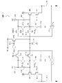
- FIG. 2 is a diagram illustrating an example of a circuit configuration of pixels in a pixel array section of the solid-state imaging device according to the first embodiment of the present technology;
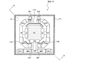
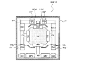
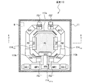
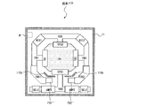
- FIG. 3 is a diagram for explaining an example of a planar layout of each element that constitutes a pixel in the pixel array section of the solid-state imaging device according to the first embodiment of the present technology;
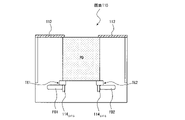
- FIG. 4 is a diagram showing an example of a schematic cross-sectional structure of the pixel shown in FIG. 3 along the IV-IV cross section.
- FIG. 1 is a block diagram showing an example of a schematic configuration of a solid-state imaging device according to an embodiment of the present technology.
- FIG. 2 is a diagram illustrating an example of a circuit configuration of pixels in a pixel array section of the solid-state imaging device according to the first embodiment of the present technology;
- FIG. 3 is a
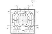
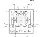
- FIG. 5A is a diagram for explaining another example of the planar layout of each element that constitutes a pixel in the pixel array section of the solid-state imaging device according to the first embodiment of the present technology
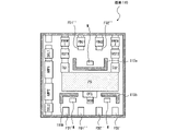
- FIG. 5B is a diagram for explaining still another example of the planar layout of each element that constitutes a pixel in the pixel array section of the solid-state imaging device according to the first embodiment of the present technology
- FIG. 6 is a diagram illustrating an example of a circuit configuration of pixels in a pixel array section of a solid-state imaging device according to a second embodiment of the present technology
- FIG. 7A is a diagram for explaining an example of a planar layout of each element that constitutes a pixel in a pixel array section of a solid-state imaging device according to a second embodiment of the present technology
- FIG. 7B is a diagram for explaining another example of the planar layout of each element that constitutes a pixel in the pixel array section of the solid-state imaging device according to the second embodiment of the present technology
- FIG. 7C is a diagram for explaining still another example of the planar layout of each element that constitutes a pixel in the pixel array section of the solid-state imaging device according to the second embodiment of the present technology
- FIG. 7A is a diagram for explaining an example of a planar layout of each element that constitutes a pixel in a pixel array section of a solid-state imaging device according to a second embodiment of the present technology
- FIG. 7B is a diagram for explaining another example of the planar layout of each element that constitutes a pixel in the pixel array section of the solid-state imaging device according
- FIG. 7D is a diagram for explaining still another example of a planar layout of each element that constitutes a pixel in the pixel array section of the solid-state imaging device according to the second embodiment of the present technology
- FIG. 7E is a diagram for explaining still another example of a planar layout of each element that constitutes a pixel in the pixel array section of the solid-state imaging device according to the second embodiment of the present technology
- FIG. 7F is a diagram for explaining still another example of a planar layout of each element that constitutes a pixel in the pixel array section of the solid-state imaging device according to the second embodiment of the present technology
- FIG. 7D is a diagram for explaining still another example of a planar layout of each element that constitutes a pixel in the pixel array section of the solid-state imaging device according to the second embodiment of the present technology
- FIG. 7E is a diagram for explaining still another example of a planar layout of each element that constitutes a pixel in the pixel array section of the solid-state imaging device
- FIG. 8A is a diagram for explaining an example of a planar layout of each element that constitutes a pixel in a pixel array section of a solid-state imaging device according to a third embodiment of the present technology
- FIG. 8B is a diagram for explaining another example of a planar layout of each element that constitutes a pixel in the pixel array section of the solid-state imaging device according to the third embodiment of the present technology
- FIG. 8C is a diagram for explaining another example of the planar layout of each element that constitutes a pixel in the pixel array section of the solid-state imaging device according to the third embodiment of the present technology
- FIG. 8A is a diagram for explaining an example of a planar layout of each element that constitutes a pixel in a pixel array section of a solid-state imaging device according to a third embodiment of the present technology
- FIG. 8B is a diagram for explaining another example of a planar layout of each element that constitutes a pixel in the pixel array section of the solid-state imaging device
- FIG. 8D is a diagram for explaining another example of the planar layout of each element that constitutes a pixel in the pixel array section of the solid-state imaging device according to the third embodiment of the present technology
- FIG. 9 is a diagram for explaining an example of a planar layout of each element that constitutes a pixel in a pixel array section of a solid-state imaging device according to a fourth embodiment of the present technology
- FIG. 10 is a diagram showing an example of a schematic cross-sectional structure of the pixel shown in FIG. 9 along the XX cross section.
- 11A is a diagram for explaining another example of the planar layout of each element that constitutes a pixel in the pixel array section of the solid-state imaging device according to the fourth embodiment of the present technology
- 11B is a diagram for explaining still another example of the planar layout of each element that constitutes a pixel in the pixel array section of the solid-state imaging device according to the fourth embodiment of the present technology
- FIG. 12A is a diagram for explaining still another example of the planar layout of each element that constitutes a pixel in the pixel array section of the solid-state imaging device according to the fourth embodiment of the present technology
- 12B is a diagram for explaining still another example of the planar layout of each element that constitutes a pixel in the pixel array section of the solid-state imaging device according to the fourth embodiment of the present technology
- FIG. 13A is a diagram for explaining an example of a planar layout of each element that constitutes a pixel in a pixel array section of a solid-state imaging device according to a fifth embodiment of the present technology
- FIG. 13B is a diagram for explaining an example of a planar layout of each element that constitutes a pixel in the pixel array section of the solid-state imaging device according to the fifth embodiment of the present technology
- FIG. 13C is a diagram for explaining an example of a planar layout of each element that constitutes a pixel in the pixel array section of the solid-state imaging device according to the fifth embodiment of the present technology
- FIG. FIG. 13C is a diagram for explaining an example of a planar layout of each element that constitutes a pixel in the pixel array section of the solid-state imaging device according to the fifth embodiment of the present technology
- FIG. 13D is a diagram for explaining an example of a planar layout of each element that constitutes a pixel in the pixel array section of the solid-state imaging device according to the fifth embodiment of the present technology
- 14A is a diagram for explaining an example of a planar layout of each element that constitutes a pixel in a pixel array section of a solid-state imaging device according to a fifth embodiment of the present technology
- FIG. 14B is a diagram for explaining an example of a planar layout of each element that constitutes a pixel in the pixel array section of the solid-state imaging device according to the fifth embodiment of the present technology
- FIG. 14C is a diagram for explaining an example of a planar layout of each element that constitutes a pixel in the pixel array unit of the solid-state imaging device according to the fifth embodiment of the present technology
- Second Embodiment (Configuration Example Using Two Charge Ejection Transistors) 3.
- Third Embodiment (Configuration Example with Another Layout of Source follower Circuit) 4.
- Fourth Embodiment (Configuration Example Using Vertical Transistors) 5.
- Fifth Embodiment (Configuration Example Using Dummy Semiconductor Structure) 6.
- Sixth Embodiment (Configuration Example without Using Feedback Enable Transistor)
- a solid-state imaging device includes a pixel having a structure that suppresses light from entering a floating diffusion region formed around a photoelectric conversion unit such as a single photodiode. do.
- this embodiment describes a pixel having a structure that suppresses light from entering the floating diffusion regions formed by the feedback enable transistor and the switching transistor, respectively.
- FIG. 1 is a block diagram showing an example of a schematic configuration of a solid-state imaging device according to one embodiment of the present technology.
- the solid-state imaging device 1 uses a photoelectric conversion element such as a photodiode that constitutes each pixel to convert the amount of charge corresponding to the intensity of the light imaged on the pixel into an electric signal, and outputs the electric signal as pixel data. It is a semiconductor device that The solid-state imaging device 1 of the present disclosure is a back-illuminated solid-state imaging device having a semiconductor element structure adapted to the indirect ToF method.
- the solid-state imaging device 1 includes, for example, a pixel array section 11, a vertical driving section 12, a column processing section 13, a horizontal driving section 14, a system control section 15, and a signal processing section 16. , and the data storage unit 17 .
- the pixel array section 11 consists of a group of pixels 110 as light receiving elements arrayed in the horizontal direction (row direction) and vertical direction (column direction).
- the pixel array unit 11 converts an amount of electric charge corresponding to the intensity of incident light formed on each pixel into an electric signal, and outputs the electric signal as a pixel signal.
- the pixel 110 includes a photodiode and several transistors formed in a semiconductor region, as will be described later.
- the pixel array section 11 can include, for example, effective pixels arranged in an area capable of receiving actual light, and dummy pixels arranged outside the area and shielded by metal or the like.
- optical elements such as a micro on-chip lens and a color filter for condensing incident light are formed on each pixel of the pixel array section 11 .
- the vertical driving section 12 is configured including circuits such as a shift register and an address decoder.
- the vertical drive unit 12 supplies drive signals and the like to each pixel through a plurality of pixel drive lines 18, thereby driving each pixel of the pixel array unit 11, for example, simultaneously or in units of rows.
- the column processing unit 13 reads pixel signals from each pixel through a vertical signal line (VSL) 19 for each pixel row (column) of the pixel array unit 11, and performs noise removal processing, correlated double sampling (CDS) processing, and A/D (Analog-to-Digital) conversion processing. Pixel signals processed by the column processing unit 13 are output to the signal processing unit 16 .
- the vertical signal line (VSL) 19 is an example of a readout signal line.
- the horizontal driving section 14 is configured including circuits such as a shift register and an address decoder.
- the horizontal driving section 14 sequentially selects pixels corresponding to the pixel rows of the column processing section 13 .
- By selective scanning by the horizontal drive unit 14 pixel signals that have undergone signal processing for each pixel in the column processing unit 13 are sequentially output to the signal processing unit 16 .
- the system control unit 15 includes a circuit such as a timing generator that generates various timing signals.
- the system control unit 15 drives and controls the vertical driving unit 12, the column processing unit 13, and the horizontal driving unit 14 based on timing signals generated by, for example, a timing generator (not shown).
- the signal processing unit 16 performs signal processing such as arithmetic processing on the pixel signals supplied from the column processing unit 13 while temporarily storing data in the data storage unit 17 as necessary. output an image signal based on
- the solid-state imaging device 1 is not limited to the configuration described above.
- the data storage unit 17 is arranged after the column processing unit 13, and the pixel signals output from the column processing unit 13 are supplied to the signal processing unit 16 via the data storage unit 17. It may be configured to As another example, the solid-state imaging device 1 may be configured such that the column processing section 13, the data storage section 17, and the signal processing section 16, which are connected in series, process each pixel signal in parallel.
- the solid-state imaging device 1 configured as described above is adapted, for example, to a distance image sensor device for acquiring a distance image based on distance information to an object.
- a range image sensor device is configured, for example, as a system-on-chip (SoC) CMOS image sensor.
- SoC system-on-chip
- the distance image sensor device is mounted on a vehicle and applied to an in-vehicle system that measures distance information to an object outside the vehicle.
- the distance image sensor device is applied to a user interface that measures the distance to a user's finger or the like and recognizes the user's gesture based on the measurement result.
- FIG. 2 is a diagram showing an example of the circuit configuration of pixels in the pixel array section of the solid-state imaging device according to the first embodiment of the present technology. That is, this figure shows an example of the circuit configuration of any one pixel (unit pixel) 110 out of the plurality of pixels 110 forming the pixel array section 11 of the solid-state imaging device 1 shown in FIG.
- the pixel 110 includes a photoelectric conversion unit PD made up of, for example, a photodiode.
- the charge generated by the photoelectric conversion unit PD can be distributed according to the intensity of the received light and output as separate pixel signals. configured to
- the pixel 110 of this example includes transfer transistors TG1 and TG2, additional capacitors CFD1 and CFD2, switching transistors FDG1 and FDG2, reset transistors RST1 and RST2, feedback enable transistors FBEN1 and FBEN2, feedback amplifier circuits FBOP1 and It includes FBOP2, amplification transistors AMP1 and AMP2, selection transistors SEL1 and SEL2, and a discharge transistor OFG.
- Floating diffusion regions FD1 and FD2 are formed between the transfer transistors TG1 and TG2 and the amplification transistors AMP1 and AMP2, respectively.
- the transfer transistors TG1 and TG2, the switching transistors FDG1 and FDG2, the reset transistors RST1 and RST2, the feedback enable transistors FBEN1 and FBEN2, the selection transistors SEL1 and SEL2, and the charge discharge transistor OFG are driven and controlled by the vertical drive section 12.
- two elements or elements such as the transfer transistors TG1 and TG2, for example, are referred to as the transfer transistor TG unless they need to be distinguished from each other. .
- the transfer transistors TG1 and TG2 are described as a pair of transistors, but the present invention is not limited to this, and may be configured by a set of three or more transistors.
- each transistor in the pixel 110 is an NMOS transistor in the present disclosure, it is not limited to this. Also, all or at least some of these transistors are made of polycrystalline silicon (hereinafter referred to as "polysilicon"). Polysilicon is advantageous for light reflection or shielding. In the present disclosure, a vertical transistor made of polysilicon can reflect or block light leaking from or passing through the photoelectric conversion part PD.
- the transfer transistor TG is a switching transistor for transferring charges generated in the photoelectric conversion unit PD to the floating diffusion region FD. That is, the transfer transistor TG1 is in a non-conducting state (off state) when the voltage of the transfer drive signal TG_S1 supplied to its gate is at a LOW level, and becomes conductive in response to the transfer drive signal TG_S1 being at a high level. state (on state), thereby transferring charges generated in the photoelectric conversion unit PD to the floating diffusion region FD1.
- the transfer transistor TG2 is in a non-conducting state (off state) when the voltage of the transfer drive signal TG_S2 supplied to its gate is at LOW level, and becomes conductive in response to the transfer drive signal TG_S2 being at high level. state (on state), thereby transferring charges generated in the photoelectric conversion unit PD to the floating diffusion region FD1.
- the transfer drive signal TG_S1 and the transfer drive signal TG_S2 have a predetermined phase difference with each other, whereby charges generated in the photoelectric conversion unit PD are transferred to the floating diffusion regions FD1 and FD2 at different timings. be.
- the floating diffusion region FD functions as a charge storage portion that temporarily holds charges generated by the photoelectric conversion portion PD and transferred therefrom. That is, in the present disclosure, charges generated in the photoelectric conversion unit PD are distributed to and accumulated in the floating diffusion regions FD1 and FD2 by the operation of the transfer transistors TG1 and TG2 with a predetermined time difference. The electric charges accumulated in the floating diffusion regions FD1 and FD2 are read at a predetermined timing as an electric signal (pixel signal) having a voltage corresponding to the amount. In the present disclosure, as will be described later, part of the floating diffusion region FD may be referred to as FD' or FD''.
- the switching transistor FDG is a switching transistor for coupling the additional capacitance CFD to the floating diffusion region FD according to the intensity of the received light. That is, the switching transistor FDG1 becomes conductive in response to the voltage of the FD drive signal FDG_S1 supplied to its gate becoming High level, thereby electrically connecting the floating diffusion region FD1 and the additional capacitance CFD1. Join. When the voltage of the FD drive signal FDG_S2 supplied to its gate becomes High level, the switching transistor FDG2 becomes conductive in response to this, thereby electrically connecting the floating diffusion region FD2 and the additional capacitance CFD2. Join.
- the additional capacitance CFD provides additional capacitance by coupling with the floating diffusion region FD according to predetermined operating conditions. For example, when the intensity of the received light is high (high illuminance), the switching transistors FDG1 and FDG2 are turned on by the FD drive signals FDG_S1 and FDG_S2, as described above, so that the floating diffusion regions FD1 and FD2 This prevents the charge from overflowing, allowing more charge to be stored. Therefore, the dynamic range of the amount of light received in the solid-state imaging device 1 is expanded.
- the additional capacitances CFD1 and CFD2 are formed by, for example, wiring capacitances.
- the reset transistor RST is a switching transistor for resetting the potential of the floating diffusion region FD. That is, the reset transistor RST1 becomes conductive in response to the voltage of the FD drive signal RST_S1 supplied to its gate becoming High level, thereby resetting the potential of the floating diffusion region FD1. Further, the reset transistor RST2 becomes conductive in response to the voltage of the FD drive signal RST_S2 supplied to its gate becoming High level, thereby resetting the potential of the floating diffusion region FD2. In this example, the switching transistor FDG also becomes conductive in conjunction with the conductive state of the reset transistor RST, and the additional capacitance CFD is reset.
- the capacitance CST is a parasitic capacitance due to the provision of the reset transistor RST.
- the feedback enable transistor FBEN is a switching transistor that configures the feedback circuit of the feedback amplifier circuit FBOP and controls the reset voltage for the purpose of noise canceling when resetting the charge of the floating diffusion region FD.
- a floating diffusion region FD1 is formed in the vicinity of the feedback enable transistor FBEN, in this example, on the distal side of the feedback enable transistor FBEN with respect to the photoelectric conversion unit PD.
- the feedback enable transistor FBEN1 becomes conductive in response to the voltage of the FBEN drive signal FBEN_S1 supplied to its gate becoming High level, whereby the reset transistor RST1 is connected to the feedback amplifier circuit FBOP1.
- the feedback amplifier circuit FBOP1 operates so as to eliminate the difference in differential input between the voltage of the vertical signal line VSL1 and the reference voltage VRef , thereby canceling the voltage noise (reset noise) to the reset transistor RST1, resulting in a floating voltage.
- the charge in the diffusion region FD1 can be reliably reset.
- the feedback enable transistor FBEN2 becomes conductive in response to the voltage of the FBEN drive signal FBEN_S2 supplied to its gate becoming High level, whereby the reset transistor RST2 is connected to the feedback amplifier circuit FBOP2. be.
- the feedback amplifier circuit FBOP1 operates so as to eliminate the difference in differential input between the voltage of the vertical signal line VSL1 and the reference voltage VRef , thereby canceling voltage noise to the reset transistor RST2 and reducing the charge in the floating diffusion region FD1. can be reliably reset.
- the capacitance CFB is a parasitic capacitance due to the provision of the feedback enable transistor FBEN, and is electrically coupled to the floating diffusion region FD.
- the amplification transistor AMP is a transistor that constitutes a source follower circuit. That is, the amplification transistor AMP1 has its source connected to the vertical signal line 19 (VSL1) through the selection transistor SEL1 and further connected to a constant current source (not shown), thereby forming a source follower circuit. .
- the amplifying transistor AMP2 has its source connected to the vertical signal line 19 (VSL2) via the selection transistor SEL2, and is further connected to a constant current source (not shown), thereby forming a source follower circuit.
- the selection transistor SEL is a switching transistor for outputting a pixel signal based on the charge accumulated in the floating diffusion region FD to the vertical signal line 19 at arbitrary timing. That is, the selection transistor SEL1 becomes conductive in response to the voltage of the selection signal SEL_S1 supplied to its gate becoming High level, whereby the pixel signal based on the charge of the floating diffusion region FD1 is transferred to the amplification transistor AMP1. and output to the vertical signal line VSL1. When the voltage of the selection signal SEL_S2 supplied to the gate of the selection transistor SEL2 becomes High level, the selection transistor SEL2 becomes conductive in response to this. and output to the vertical signal line VSL2.
- the charge discharge transistor OFG is a switching transistor for discharging charges remaining in the photoelectric conversion unit PD. That is, when the voltage of the charge discharge drive signal OFG_S supplied to its gate becomes High level, the charge discharge transistor OFG becomes conductive in response to this, whereby the potential of the photoelectric conversion unit PD becomes VDD. Charge is discharged.
- the charge discharge transistor OFG can have a vertical structure formed by stacking semiconductor films. Such transistors are called vertical transistors. Thereby, the charge discharge transistor OFG reflects the light leaked from the photoelectric conversion unit PD toward the photoelectric conversion unit PD, thereby promoting the reuse of light in the photoelectric conversion unit PD, and the floating diffusion region FD1''. and effectively suppresses light from entering the FD2''. Note that as shown in other embodiments, a plurality of charge discharge transistors OFG may be provided in order to facilitate discharge of charges accumulated in the photoelectric conversion unit PD.
- FIG. 3 is a diagram for explaining an example of a planar layout of each element that constitutes a pixel in the pixel array section of the solid-state imaging device according to the first embodiment of the present technology.
- the figure shows a planar layout when viewed from the surface of the pixel 110 (incident surface or light receiving surface) on which light is incident.
- 4 is a diagram showing an example of a schematic cross-sectional structure of the pixel shown in FIG. 3 along the IV-IV cross section.
- a plane parallel to the incident surface of the pixel 110 is called the XY plane
- a direction perpendicular to the XY plane is called the Z direction or depth direction.
- the pixel 110 has, for example, a substantially rectangular outer edge shape in plan view (on the XY plane). That is, the pixel 110 includes a semiconductor region defined in a substantially rectangular shape by the pixel separating portion 111 .
- a photoelectric conversion unit PD is formed substantially in the center of the pixel 110 . In this example, the photoelectric conversion part PD is formed in an octagonal shape.
- a well contact W is formed in one corner of the pixel isolation portion 111 . The well contact W is preferably formed in the vicinity of the floating diffusion region FD in order to suppress fluctuations in the potential of the floating diffusion region FD.
- a light shielding lid 112 is formed on the upper surface (light receiving surface) of the pixel 110 .
- the light-shielding lid 112 is a structure made of, for example, an oxide insulating film having a light-shielding property provided in front of the pixel for preventing incident light from entering a region other than the photoelectric conversion unit PD described later.
- the light-receiving surface of the pixel 110 is provided with optical elements such as a color filter and an on-chip lens.
- the pixel isolation portion 111 is a trench-like structure that is provided between adjacent pixels 110 and electrically and optically isolates the pixels 110 from each other. Therefore, one side of the pixel 110 is shared with the pixel isolation portion 111 of the adjacent pixel.
- the pixel separation unit 111 prevents crosstalk between adjacent pixels 110 and suppresses deterioration in image quality.
- the pixel separation portion 111 is an insulating single-layer film or multilayer film such as silicon oxide (SiO 2 ), tantalum oxide (Ta 2 O 5 ), hafnium oxide (HfO 2 ), or aluminum oxide (Al 2 O 3 ). formed by Such an insulating pixel separation section 111 is called DTI (Deep Trench Isolation).
- the pixel separation section 111 may be made of a metal with high light shielding properties, such as tantalum (Ta), aluminum (Al), silver (Ag), gold (Au), or copper (Cu). It may be made of polysilicon.
- the above-described various transistors and the like are arranged around the photoelectric conversion unit PD. That is, the transfer transistors TG1 and TG2 are formed near the pair of ends of the photoelectric conversion part PD, respectively, and the floating diffusion regions FD1 and FD2 are formed outside thereof. In this example, the floating diffusion regions FD1 and FD2 are formed along the periphery of the photoelectric conversion part PD so as to partially surround it.
- a power supply wiring pattern VDD formed in a wiring layer and a charge discharging transistor OFG electrically connected to the power supply wiring pattern VDD are formed near the other end of the photoelectric conversion unit PD.
- the wiring layer can reflect the light leaked from the photoelectric conversion unit PD and contribute to the reuse of the light from the photoelectric conversion unit PD. Furthermore, in the drawing, amplification transistors AMP1 and AMP2 and selection transistors SEL1 and SEL2 are formed so as to overlap the extending power wiring pattern VDD in the Z direction. Incidentally, in this example, the feedback amplifier circuit FBOP is not shown in the figure because it is formed at a distant position through the wiring layer.
- Reset transistors RST1 and RST2 feedback enable transistors FBEN1 and FBEN2, and switching transistors FDG1 and FDG2 are formed around the photoelectric conversion unit PD so as to overlap the floating diffusion regions FD1 and FD2 in the Z direction.
- floating diffusion regions FD1' and FD2' and FD1'' and FD2'' are formed to extend near the feedback enable transistors FBEN1 and FBEN2 and the switching transistors FDG1 and FDG2, respectively.
- the floating diffusion region FD' is formed on the distal side of the feedback enable transistors FBEN1 and FBEN2 with respect to the photoelectric conversion unit PD, while the floating diffusion region FD'' is formed with the pair of switching transistors FDG1. It is formed between FDG2.
- the switching transistor FDG of this example is a vertical transistor having a vertical structure in which semiconductor films are stacked in the Z direction (see FIG. 4). Furthermore, the switching transistor FDG is configured to have a bent portion along the outer peripheral edge of the photoelectric conversion unit PD in plan view. As a result, the switching transistor FDG reflects light leaked from the photoelectric conversion unit PD (some of which may include reflected light from the wiring layer) toward the photoelectric conversion unit PD, thereby causing the floating diffusion region FD1 to '' and FD2'' are effectively suppressed, and the reuse of light in the photoelectric conversion part PD is promoted.
- a shielding portion 113a is provided between the photoelectric conversion portion PD and the feedback enable transistors FBEN1 and FBEN2.
- the shielding part 113a is, for example, a trench-like structure that shields or reflects light that leaks from the photoelectric conversion part PD and travels toward the floating diffusion regions FD1' and FD2' formed in the vicinity of the feedback enable transistors FBEN1 and FBEN2.
- the shielding part 113a is formed along the outer peripheral edge of the photoelectric conversion part PD.
- the shielding portion 113a extends deeply in the Z direction so as to effectively shield or reflect the light directed toward the floating diffusion regions FD1' and FD2'.
- the light reflected by the shielding portion 113a is incident on the photoelectric conversion portion PD, is reused, and can contribute to the generation of charges.
- feedback enable transistor FBEN may be a vertical transistor. As a result, the light leaking from the photoelectric conversion part PD and directed to the floating diffusion regions FD1' and FD2' can be reliably blocked.
- a shielding portion 113b is provided between the photoelectric conversion portion PD and the switching transistors FDG1 and FDG2.
- the shielding part 113b is, for example, a trench-like structure that shields or reflects light that leaks from the photoelectric conversion part PD and travels toward the floating diffusion regions FD1'' and FD2'' formed in the vicinity of the switching transistors FDG1 and FDG2. .
- the shielding part 113b is formed along the outer peripheral edge of the photoelectric conversion part PD.
- the shielding portion 113b also extends deeply in the Z direction so as to effectively shield or reflect light directed toward the floating diffusion regions FD1'' and FD2''. The light reflected by the shielding portion 113b is incident on the photoelectric conversion portion PD, is reused, and can contribute to the generation of charges.
- the shielding portion 113 is made of, for example, silicon oxide (SiO 2 ), tantalum oxide (Ta 2 O 5 ), hafnium oxide (HfO 2 ), aluminum oxide (Al 2 O 3 ), or the like, similar to the pixel separation portion 111 described above.
- the shielding part 113a is formed of, but not limited to, an insulating single-layer film or multilayer film. It may be made of a highly light-shielding metal such as (Cu), or it may be made of polysilicon (polycrystalline silicon).
- the shielding portion 113 has a bent portion formed along the outer peripheral edge of the photoelectric conversion portion PD. Note that the shape and arrangement of the shielding portion 113 can take various forms, as will be described later.
- unintended entry of light into the floating diffusion region FD in the pixel 110 can be reliably suppressed.
- the shielding portion 113a is provided between the photoelectric conversion portion PD and the feedback enable transistor FBEN, the light leaked from the photoelectric conversion portion PD is directed toward the photoelectric conversion portion PD. It is possible to reliably suppress light from entering the floating diffusion region FD′ formed in the vicinity of the feedback enable transistor FBEN and to promote reuse of light in the photoelectric conversion unit PD.
- the shielding portion 113b is provided between the photoelectric conversion unit PD and the switching transistor FDG, similarly, light leaked from the photoelectric conversion unit PD is reflected toward the photoelectric conversion unit PD, Intrusion of light into the floating diffusion region FD'' formed in the vicinity of the transistor FDG can be reliably suppressed, and reuse of light in the photoelectric conversion unit PD can be promoted.
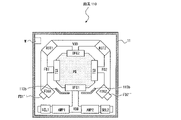
- FIG. 5A is a diagram for explaining another example of the planar layout of each element that constitutes a pixel in the pixel array section of the solid-state imaging device according to the first embodiment of the present technology;
- the shape of the switching transistor FDG is different, and the neighboring floating diffusion region FD'' is formed at a different position.
- the switching transistors FDG1 and FDG2 are formed in a substantially rectangular shape in plan view. In other words, the switching transistors FDG1 and FDG2 of this example do not have bent portions like the example described above. Note that the switching transistors FDG1 and FDG2 are preferably formed as vertical transistors.
- the floating diffusion regions FD1'' and FD2'' near the switching transistors FDG1 and FDG2 are formed on the distal side with respect to the photoelectric conversion unit PD. That is, the floating diffusion regions FD1'' and FD2'' are formed behind the switching transistors FDG1 and FDG2 formed obliquely with respect to the pixel isolation portion 111 in a plan view. Also, the shielding portions 113b1 and 113b2 are formed in portions where the switching transistors FDG1 and FDG2 substantially face the photoelectric conversion portion PD.
- the floating diffusion region FD'' formed in the vicinity of the switching transistor FDG is formed on the distal side of the switching transistor FDG with respect to the photoelectric conversion unit PD. Intrusion of light into the FD'' can be reliably suppressed, and the light receiving region of the photoelectric conversion unit PD can be made wider. Further, when the switching transistor FDG is formed as a vertical transistor, it is possible to more effectively and reliably suppress the entry of light.
- FIG. 5B is a diagram for explaining still another example of the planar layout of each element that constitutes a pixel in the pixel array section of the solid-state imaging device according to the first embodiment of the present technology; This example is a further modification of Modification 1-2 above, in which the floating diffusion region FD'' near the switching transistor FDG is formed at a different position.
- the switching transistor FDG of this example is provided substantially parallel to the pixel separation section 111 in plan view.
- a floating diffusion region FD′′ in the vicinity of the switching transistor FDG is formed so as to face the pixel isolation portion 111 . That is, the floating diffusion region FD'' is formed farther from the photoelectric conversion part PD.
- the floating diffusion region FD'' formed in the vicinity of the switching transistor FDG is provided on the distal side of the switching transistor FDG with respect to the photoelectric conversion unit PD and at a position facing the pixel separation unit 111. Therefore, the switching transistor FDG can reliably suppress light from entering the floating diffusion region FD'', and the light receiving region of the photoelectric conversion unit PD can be further increased. can be wide.
- Second Embodiment is a modification of the above-described first embodiment, and is a solid-state imaging device having pixels having a structure in which two charge discharge transistors are arranged around a photoelectric conversion unit PD. Characterized by
- FIG. 6 is a diagram showing an example of the circuit configuration of pixels in the pixel array section of the solid-state imaging device according to the second embodiment of the present technology. That is, this figure shows an example of the circuit configuration of any one pixel (unit pixel) 110 out of the plurality of pixels 110 forming the pixel array section 11 of the solid-state imaging device 1 shown in FIG.
- charge discharge transistors OFG1 and OFD2 for discharging charges accumulated in the photoelectric conversion unit PD are connected to the photoelectric conversion unit PD.
- Charge drain transistors OFG1 and OFD2 may be formed as vertical transistors.
- the charge discharge transistors OFG1 and OFD2 may be the same, or may differ in size (for example, the thickness of the gate insulating film).
- the charge discharge transistors OFG1 and OFD2 both become conductive in response to this, whereby the potential of the photoelectric conversion part PD becomes equal to VDD. charge is discharged.
- the two charge discharge transistors OFG1 and OFD2 are provided, so that the potential of the photoelectric conversion unit PD can be reset at a higher speed.
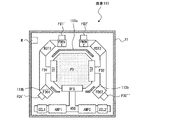
- FIG. 7A is a diagram for explaining an example of a planar layout of each element that constitutes a pixel in the pixel array section of the solid-state imaging device according to the second embodiment of the present technology.
- transfer transistors TG1 and TG2 are formed near one end of a pair of photoelectric conversion units PD, respectively, while a pair of transfer transistors different from the one end of the pair are formed.
- Charge discharge transistors OFG1 and OFD2 are formed near the other end. That is, the charge discharge transistor OFD2 is formed in the vicinity of the feedback enable transistor FBEN.
- the VDD wiring pattern extends to substantially directly under the charge discharge transistor OFD2 in the wiring layer, and electrically connects the charge discharge transistor OFD2.
- shielding portions 113a1 and 113a2 are provided to shield light leaking from the photoelectric conversion portion PD and traveling toward the floating diffusion region FD' in the vicinity of the feedback enable transistors FBEN1 and FBEN2.
- the shielding portions 113a1 and 113a2 may be configured as one continuous shielding portion 113a.
- the same advantages and effects as those of the first embodiment can be obtained.
- the charge discharge transistor OFG2 formed as a vertical transistor is arranged in the vicinity of the feedback enable transistor FEBN, the light leaked from the photoelectric conversion unit PD is directed toward the photoelectric conversion unit PD. The light is reflected, thereby promoting reuse of light in the photoelectric conversion part PD and effectively suppressing light from entering the floating diffusion region FD.
- FIG. 7B is a diagram for explaining another example of the planar layout of each element that constitutes a pixel in the pixel array section of the solid-state imaging device according to the second embodiment of the present technology;
- the switching transistor FDG is formed in a structure having no curved portion, as in the modification 1-1.
- the switching transistors FDG1 and FDG2 are formed in a substantially rectangular shape in plan view.
- the switching transistors FDG1 and FDG2 of this example do not have bent portions like the example described above.
- the switching transistors FDG1 and FDG2 are preferably formed as vertical transistors.
- the floating diffusion regions FD1'' and FD2'' near the switching transistors FDG1 and FDG2 are formed on the distal side with respect to the photoelectric conversion unit PD.
- the floating diffusion regions FD1'' and FD2'' are formed behind the switching transistors FDG1 and FDG2 obliquely with respect to the pixel isolation portion 111 in plan view.
- the shielding portions 113b1 and 131b2 are formed in portions where the switching transistors FDG1 and FDG2 substantially face the photoelectric conversion portion PD.
- the floating diffusion region FD'' formed in the vicinity of the switching transistor FDG is formed on the distal side of the switching transistor FDG with respect to the photoelectric conversion unit PD. Intrusion of light into the FD'' can be reliably suppressed, and the light-receiving region of the photoelectric conversion part PD can be made wider. Further, when the switching transistor FDG is formed as a vertical transistor, it is possible to more effectively and reliably suppress the entry of light. (Modification 2-2) FIG.
- FIG. 7C is a diagram for explaining still another example of the planar layout of each element that constitutes a pixel in the pixel array section of the solid-state imaging device according to the second embodiment of the present technology.
- This example is a further modification of Modification 1-2, in which the floating diffusion region FD'' in the vicinity of the switching transistor FDG is formed at a position further away from the photoelectric conversion part PD.
- the switching transistor FDG of this example is provided substantially parallel to the pixel separation section 111 in plan view.
- a floating diffusion region FD′′ in the vicinity of the switching transistor FDG is provided so as to face the pixel separation portion 111 . Therefore, the floating diffusion region FD'' is formed farther from the photoelectric conversion part PD.
- the floating diffusion region FD'' formed in the vicinity of the switching transistor FDG is provided on the distal side of the switching transistor FDG with respect to the photoelectric conversion unit PD and at a position facing the pixel separation unit 111. Therefore, the switching transistor FDG can reliably suppress light from entering the floating diffusion region FD'', and the light receiving region of the photoelectric conversion unit PD can be further increased. can be wide.
- FIG. 7D is a diagram for explaining still another example of a planar layout of each element that constitutes a pixel in the pixel array section of the solid-state imaging device according to the second embodiment of the present technology;
- the floating diffusion region FD' is formed between the feedback enable transistors FBEN.
- the floating diffusion regions FD' of this example are formed between the feedback enable transistors FBEN1 and FBEN2 so as to face each other along one end of the photoelectric conversion unit PD in plan view. formed. That is, the floating diffusion region FD' is formed between a pair of feedback enable transistors FBEN1 and FBEN2. Thereby, each transistor in the pixel 110 can be arranged more efficiently.
- the floating diffusion region FD' is formed at a position closer to one end of the photoelectric conversion unit PD than in the above example, but the shielding units 113a1 and 131a2 and the charge discharge transistor OFG2 As a result, it is possible to suppress the entry of light and to widen the light receiving area of the photoelectric conversion part PD.
- FIG. 7E is a diagram for explaining still another example of a planar layout of each element that constitutes a pixel in the pixel array section of the solid-state imaging device according to the second embodiment of the present technology;
- the floating diffusion regions FD'' near the switching transistor FDG are formed at different positions.
- the floating diffusion regions FD1'' and FD2'' near the switching transistors FDG1 and FDG2 are formed behind the switching transistors FDG1 and FDG2 formed obliquely with respect to the pixel isolation portion 111 in plan view.
- the shielding portions 113b1 and 131b2 are formed in portions where the switching transistors FDG1 and FDG2 substantially face the photoelectric conversion portion PD.
- the floating diffusion region FD'' formed in the vicinity of the switching transistor FDG is formed on the distal side of the switching transistor FDG with respect to the photoelectric conversion unit PD. Intrusion of light into the FD'' can be reliably suppressed, and the light receiving region of the photoelectric conversion unit PD can be made wider.
- FIG. 7F is a diagram for explaining still another example of a planar layout of each element that constitutes a pixel in the pixel array section of the solid-state imaging device according to the first embodiment of the present technology;
- the floating diffusion regions FD'' near the switching transistor FDG are formed at different positions.
- the switching transistor FDG of this example is provided substantially parallel to the pixel separation section 111 in plan view.
- a floating diffusion region FD′′ in the vicinity of the switching transistor FDG is formed so as to face the pixel isolation portion 111 . Therefore, the floating diffusion region FD'' is formed farther from the photoelectric conversion part PD.
- the floating diffusion region FD'' formed in the vicinity of the switching transistor FDG is provided on the distal side of the switching transistor FDG with respect to the photoelectric conversion unit PD and at a position facing the pixel separation unit 111. Therefore, the switching transistor FDG can reliably suppress light from entering the floating diffusion region FD'', and the light receiving region of the photoelectric conversion unit PD can be further increased. can be wide.
- This embodiment is a modification of the above embodiment, and is characterized in that the amplifying transistor AMP and the selecting transistor SEL forming the source follower circuit are formed at different positions.
- FIG. 8A is a diagram for explaining an example of a planar layout of each element that constitutes a pixel in the pixel array section of the solid-state imaging device according to the third embodiment of the present technology
- the amplification transistor AMP and the selection transistor SEL are provided parallel to one side of the pixel separation section 111 orthogonal to the line connecting the transfer transistors TG1 and TG2. Therefore, since the distance between the transfer transistors TG1 and TG2 is narrowed, the electric field of the photoelectric conversion unit PD is increased, and the charge distribution capability is improved.
- the wiring distance between the transfer transistor TG2, the amplification transistor AMP2, and the selection transistor SEL2 is long. Therefore, the amplification transistor AMP2 and the selection transistor SEL2 in the other pixel 110 positioned on the transfer transistor TG2 side are configured to read out the floating diffusion region FD2 that accumulates the charges transferred from the transfer transistor TG2 in the one pixel 110. be.
- Modification 8B to 8D are diagrams for explaining another example of the planar layout of each element that constitutes a pixel in the pixel array section of the solid-state imaging device according to the third embodiment of the present technology; FIG. The examples shown in these figures correspond to the various planar layouts described above and have the same advantages and effects, so description thereof will be omitted.
- the pixel 110 configured as described above, it is possible to reliably suppress unintended entry of light into the floating diffusion region FD in the pixel 110, as in the above-described example.
- the distance between the transfer transistors TG1 and TG2 provided at the pair of ends of the photoelectric conversion unit PD is reduced, the electric field of the photoelectric conversion unit PD is increased, and the charge distribution capability is improved.
- This embodiment is a modification of the above embodiments, and is characterized in that some transistors in a pixel are configured as vertical transistors. As will be described below, the structure of the vertical transistor is appropriately determined in consideration of light shielding properties and charge transfer efficiency.
- FIG. 9 is a diagram for explaining an example of a planar layout of each element that constitutes a pixel in the pixel array section of the solid-state imaging device according to the fourth embodiment of the present technology.
- 10 is a diagram showing an example of a schematic cross-sectional structure of the pixel shown in FIG. 9 along the XX cross section.
- the transfer transistor TG and the charge discharge transistor OFG are formed as vertical transistors having an embedded structure 114 in part thereof. Also, although not shown, a gate oxide film is formed under the embedded structure 114 .
- the embedded structure 114 TG of the transfer transistor TG reflects or shields the light that leaks from the photoelectric conversion unit PD and travels toward the floating diffusion region FD.
- the light reflected by the embedded structure 114 TG enters the photoelectric conversion unit PD and is reused.
- the transfer transistor TG transfers charges generated in the photoelectric conversion unit PD to the floating diffusion region FD when the transfer drive signal TG_S supplied to its gate becomes High level.
- the charge of the photoelectric conversion unit PD is transferred to the floating diffusion region FD through the silicon layer under the buried structure 114 TG , so that the flow is slightly suppressed and the charge transfer efficiency is lowered.
- the light that leaks from the photoelectric conversion part PD and travels toward the floating diffusion region FD is effectively reflected or blocked, so that deterioration of image quality can be prevented.
- the buried structure 114 OFG of the charge drain transistor OFG reflects or blocks light from going to the floating diffusion region FD'' near the switching transistor FDG.
- the light reflected by the embedded structure 114 OFG is incident on the photoelectric conversion unit PD and reused.
- the charge discharge transistor OFG discharges the potential of the photoelectric conversion unit PD when the charge discharge drive signal OFG_S supplied to its gate becomes High level.
- the transfer transistor TG and the charge discharge transistor OFG of this example are formed as vertical transistors, the entry of light into the floating diffusion region FD is reliably suppressed, and the light is transferred to the photoelectric conversion unit PD. It can be re-entered and reused.
- the embedded structure 114 of the transfer transistor TG and/or the charge discharge transistor OFG can take various forms in consideration of the light shielding property and the charge transfer efficiency.
- FIG. 11A is a diagram for explaining another example of a planar layout of each element that constitutes a pixel in the pixel array section of the solid-state imaging device according to the fourth embodiment of the present technology;
- the embedded structure 114 of the transfer transistor TG and the charge discharge transistor OFG is formed in a so-called comb shape or columnar shape (indicated by small square dotted lines in the figure). That is, the embedded structure 114 of this example partially has a gap in the Z direction (depth direction).
- Such a comb-like embedded structure 114 allows electric charges to pass through the gaps, so that it is possible to prevent an excessive decrease in charge transfer efficiency while considering the light shielding property.
- FIG. 11B is a diagram for explaining still another example of the planar layout of each element that constitutes a pixel in the pixel array section of the solid-state imaging device according to the fourth embodiment of the present technology.
- the embedded structure 114 of the transfer transistor TG and the charge discharge transistor OFG is formed in a zigzag shape in plan view. Since the embedded structure 114 of this example has fewer gaps than the comb-shaped embedded structure 114 of FIG. 11A, it is possible to appropriately adjust the balance between the light shielding property and the charge transfer efficiency.
- (Modification 4-2) 12A and 12B are diagrams for explaining still another example of the planar layout of each element that constitutes a pixel in the pixel array section of the solid-state imaging device according to the fourth embodiment of the present technology.
- the vertical transistor can be applied not only to the transfer transistor TG and/or the charge discharge transistor OFG, but also to the switching transistor FDG, for example. That is, the switching transistor FDG of this example is configured as a vertical transistor having a buried structure 114 FDG in its part.
- This embodiment is a modification of the above-described embodiments, and is characterized in that the shielding portion 113 is formed by dummy transistors having a vertical structure.
- a dummy transistor is a transistor that has a semiconductor lamination structure and is not electrically connected to any wiring pattern.
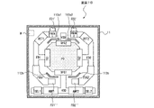
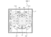
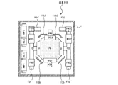
- FIGS. 13A to 13D are diagrams for explaining an example of a planar layout of each element constituting a pixel in the pixel array section of the solid-state imaging device according to the fifth embodiment of the present technology.
- a dummy transistor 115a is formed along one end of the photoelectric conversion unit PD between the transfer transistors TG1 and TG2. This makes it possible to suppress light leaking from the photoelectric conversion unit PD from entering the floating diffusion region FD near the transfer transistor TG and the FD'' near the switching transistor FDG.
- Dummy transistors 115b1 and 115b2 are formed on both sides of the charge discharge transistor OFG. That is, the dummy transistors 115b1 and 115b2 extend from the adjacent pixel 110 to the floating diffusion regions FD1′ and FD2′ near the feedback enable transistors FBEN1 and FBEN2 and the floating diffusion regions FD1′′ near the switching transistors FDG1 and FDG2. and FD2'', along one end of the photoelectric conversion part PD.
- a semiconductor conductive region (well) is electrically connected to the distal side of the dummy transistors 115a and 115b with respect to the photoelectric conversion unit PD, that is, in the vicinity of the floating diffusion regions FD, FD', and FD''.
- a well contact W is formed for direct connection. This can reduce potential fluctuations in the floating diffusion regions FD, FD', and FD''.
- FIG. 13B shows an example in which dummy transistors 115a and 115b each have a bent portion. This makes it possible to further suppress the intrusion of light.
- 13C and 13D show an example in which the well contact W is arranged near the photoelectric conversion part PD.
- the dummy transistors 115a and 115b can be arranged closer to the floating diffusion regions FD, FD', and FD'', thereby further suppressing light from entering.
- This embodiment shows an example of a pixel in which the feedback enable transistor FBEN is omitted.
- FIGS. 14A to 14C are diagrams for explaining an example of a planar layout of each element constituting a pixel in the pixel array section of the solid-state imaging device according to the fifth embodiment of the present technology.
- the pixel 110 of this embodiment differs from the above embodiments in that the feedback enable transistor FBEN is omitted. Also, in this example, an example using two charge discharge transistors OFG is shown.
- the present technology can be applied to various pixels 110 that omit the feedback enable transistor FBEN.
- steps, operations or functions may be performed in parallel or in a different order so long as the results are not inconsistent.
- the steps, acts and functions described are provided as examples only and some of the steps, acts and functions may be omitted or combined together without departing from the scope of the invention. one, and other steps, operations, or functions may be added.
- a solid-state imaging device comprising a pixel array section in which a plurality of pixels are arranged in an array, each of the plurality of pixels, a pixel separating portion defining an outer edge shape of the pixel and formed between the adjacent pixels; a photoelectric conversion unit that generates an amount of charge corresponding to light incident from the outside; a plurality of transistors including a transfer transistor formed at one end of the photoelectric conversion unit and configured to transfer the charge generated by the photoelectric conversion unit; a floating diffusion region formed around the photoelectric conversion unit for temporarily accumulating charges generated and transferred by the photoelectric conversion unit; a shielding portion formed around the photoelectric conversion portion and shielding light leaking from the photoelectric conversion portion and directed to the floating diffusion region; the plurality of transistors, a reset transistor for resetting the potential of the floating diffusion region; a feedback enable transistor connected to a feedback amplifier circuit for canceling voltage noise to the reset transistor;
- the shielding portion includes a first shielding portion that shields light
- Solid-state imaging device (2) The shielding portion is formed so as to reflect light leaking from the photoelectric conversion portion toward the photoelectric conversion portion.
- (3) The shielding portion has a bent portion formed along the outer peripheral edge of the photoelectric conversion portion, The solid-state imaging device according to (1) or (2).
- the plurality of transistors further includes a switching transistor formed around the photoelectric conversion unit for electrically coupling the floating diffusion region to an additional capacitance;
- the shielding part further includes a second shielding part that shields light directed toward another part of the floating diffusion region formed in the vicinity of the switching transistor,
- the switching transistor is configured as a vertical transistor made of polycrystalline silicon;
- the other portion of the floating diffusion region formed near the switching transistor is formed to face between the pair of switching transistors,
- the other part of the floating diffusion region formed near the switching transistor is formed on the distal side of the switching transistor with respect to the photoelectric conversion unit,
- the plurality of transistors further includes at least one charge discharge transistor formed at the other end portion of the photoelectric conversion portion, which is different from the one end portion of the photoelectric conversion portion, for discharging charges remaining in the photoelectric conversion portion,
- the charge ejection transistor is configured as a vertical transistor made of polycrystalline silicon;
- the vertical structure of the charge ejection transistor has a partial gap in the depth direction of the pixel;
- the transfer transistor is configured as a vertical transistor made of polycrystalline silicon;
- the vertical structure of the transfer transistor partially has a gap in the plane of the depth direction of the pixel;
- the shielding part is a dummy transistor having a semiconductor laminated structure made of polycrystalline silicon, The solid-state imaging device according to any one of (1) to (16).
- a well contact for electrically connecting to a semiconductor conductive region of the pixel is formed near the floating diffusion region;
- the transfer transistor is configured as a pair of transistors for distributing the charges generated by the photoelectric conversion unit to the pair of floating diffusion regions at a predetermined timing, The solid-state imaging device according to any one of (1) to (18) above.
- a distance image sensor device for obtaining a distance image based on distance information to an object obtained by the solid-state imaging device according to any one of (1) to (19).
- Solid-state imaging device 11 Pixel array part 110... Pixel 111... Pixel separation part 112... Light-shielding cover 113, 113a, 113b... Shielding part 114, 114 TG , 114 OFG ... Embedding structure 115... Dummy transistor 12... Vertical drive part 13 ... column processing section 14 ... horizontal driving section 15 ... system control section 16 ... signal processing section 17 ... data storage section 18 ... pixel drive line 19, VSL ... vertical signal line TG ... transfer transistor, FDG ... switching transistor, RST ... reset transistor , FBEN...feedback enable transistor, FBOP...feedback amplifier circuit, AMP...amplification transistor, SEL...selection transistor, OFG...charge discharge transistor, FD...floating diffusion region
Landscapes
- Engineering & Computer Science (AREA)
- Physics & Mathematics (AREA)
- Computer Networks & Wireless Communication (AREA)
- General Physics & Mathematics (AREA)
- Radar, Positioning & Navigation (AREA)
- Remote Sensing (AREA)
- Electromagnetism (AREA)
- Multimedia (AREA)
- Signal Processing (AREA)
- Solid State Image Pick-Up Elements (AREA)
- Transforming Light Signals Into Electric Signals (AREA)
Abstract
本発明は、画素がアレイ状に配置された固体撮像装置である。各画素は、隣接する前記画素間に形成された画素分離部と、入射光に応じた電荷を生成する光電変換部と、前記光電変換部により生成された電荷を転送するための転送トランジスタを含む複数のトランジスタと、前記光電変換部から転送される電荷を一時的に蓄積する浮遊拡散領域と、前記光電変換部から前記浮遊拡散領域へ向かう光を遮蔽する遮蔽部とを備える。前記複数のトランジスタは、前記浮遊拡散領域の電位をリセットするためのリセットトランジスタと、前記リセットトランジスタに対する電圧ノイズをキャンセリングするための帰還増幅回路に接続された帰還イネーブルトランジスタとを更に含む。前記遮蔽部は前記帰還イネーブルトランジスタ近傍に形成された前記浮遊拡散領域の一部に向かう光を遮蔽する。
Description
本技術は、固体撮像装置に関する。
固体撮像装置は、光を受光するための各画素(受光画素)を構成するフォトダイオード等の光電変換素子を用いて、該画素に結像した光の強弱に応じた電荷量を電気信号に変換する半導体装置である。入射光の利用効率の観点から、光の入射面(受光面)と光電変換素子との間に金属配線層を配置しない裏面照射型固体撮像装置が広く用いられている。
このような裏面照射型固体撮像装置では、隣接する画素どうしで入射した光が混ざりあうクロストークが発生し、これにより、解像度や色再現性の低下、輝度段差といった画質の低下を招いてしまうことが知られている。したがって、クロストークによるこのような画質低下を回避するために、各画素間にトレンチ構造の画素分離部を設けて、電気的・光学的に画素を分離するように設計される。また、画素内において、光電変換素子の近傍に形成された浮遊拡散(フローティングディフュージョン)領域に光が入り込むと、意図しない電荷が生成されるため、光電変換素子から電荷を引き込まない状態であっても、意図しない電荷に基づく電気信号を検出してしまい、とりわけ低光量時の画質に悪影響を及ぼす。したがって、このような画像品質の低下を防止するためにも、画素内に形成される浮遊拡散領域へ光が入り込まないようにするための対策が必要になる。
例えば、下記特許文献1は、電荷蓄積部として機能する浮遊拡散領域に対する迷光を抑止する撮像装置を開示する。
また、下記特許文献2は、フォトダイオードから電荷蓄積部への電荷転送路を保持しつつ、低コストで電荷蓄積部を遮光することができるようにする撮像装置を開示する。
更に、下記特許文献3は、隣接する画素領域間における不要光の入射を抑制し、より優れた撮像性能を発揮することのできる撮像装置を開示する。
裏面照射型固体撮像装置では、上述したように、電荷蓄積部である浮遊拡散領域に対する意図しない光の入り込みが発生し、画像品質が低下してしまうという問題がある。とりわけ、間接ToF方式に適合された裏面照射型固体撮像装置では、画素内の光電変換素子で生成された電荷を複数のゲートの開閉タイミングに応じてそれぞれの電荷蓄積部に振り分けるために光電変換素子の周囲に各種のトランジスタ素子等を多数配置する必要があり、その配置構造が複雑化している。
例えば、裏面照射型固体撮像装置の画素内には、浮遊拡散領域の電荷をリセットする際のノイズキャンセリングを目的とした帰還駆動機構が設けられる。この帰還駆動機構を構成するトランジスタの配置は、追加的な浮遊拡散領域を形成することになる。
しかしながら、上記特許文献のいずれも、帰還駆動機構を構成するトランジスタを配置した追加的な浮遊拡散領域への光の入り込みを何ら考慮していなかった。このため、このような追加的な浮遊拡散領域への光の入り込みによる画質低下が問題となっていた。
そこで、本開示は、裏面照射型固体撮像装置において、画素に形成される浮遊拡散領域への意図しない光の入り込みを確実に抑制する技術を提案することを目的とする。
より具体的には、本開示は、裏面照射型固体撮像装置において、画素内に配置されるトランジスタの近傍に形成される追加的な浮遊拡散領域への意図しない光の入り込みを確実に抑制する技術を提案することを目的とする。
とりわけ、本開示は、裏面照射型固体撮像装置において、画素内に配置される帰還駆動機構を構成するトランジスタにより形成される追加的な浮遊拡散領域への意図しない光の入り込みを確実に抑制する技術を提案することを目的とする。
上記課題を解決するための本技術は、以下に示す発明特定事項乃至は技術的特徴を含んで構成される。
ある観点に従う本技術は、複数の画素がアレイ状に配置された画素アレイ部を備える固体撮像装置である。前記複数の画素のそれぞれは、前記画素の外縁形状を画定し、隣接する前記画素の間に形成された画素分離部と、外部から入射した光に応じた量の電荷を生成する光電変換部と、前記光電変換部の一端部に形成され、前記光電変換部により生成された前記電荷を転送するための転送トランジスタを含む、複数のトランジスタと、前記光電変換部の周囲に形成され、前記光電変換部により生成され転送される電荷を一時的に蓄積する浮遊拡散領域と、前記光電変換部の周囲に形成され、前記光電変換部から漏出し前記浮遊拡散領域へ向かう光を遮蔽する遮蔽部とを備える。前記複数のトランジスタは、前記浮遊拡散領域の電位をリセットするためのリセットトランジスタと、前記リセットトランジスタに対する電圧ノイズをキャンセリングするための帰還増幅回路に接続された帰還イネーブルトランジスタとを更に含む。そして、前記遮蔽部は、前記帰還イネーブルトランジスタの近傍に形成された前記浮遊拡散領域の一部に向かう光を遮蔽する。
なお、本開示において、「システム」とは、複数の装置(又は特定の機能を実現する機能モジュール)が論理的に集合した物のことをいい、各装置や機能モジュールが単一の筐体内にあるか否かは特に問わない。
本技術の他の技術的特徴、目的、及び作用効果乃至は利点は、添付した図面を参照して説明される以下の実施形態により明らかにされる。本開示に記載された効果はあくまで例示であって限定されるものではなく、また他の効果があっても良い。
本技術の他の技術的特徴、目的、及び作用効果乃至は利点は、添付した図面を参照して説明される以下の実施形態により明らかにされる。本開示に記載された効果はあくまで例示であって限定されるものではなく、また他の効果があっても良い。
以下、図面を参照して本技術の実施の形態を説明する。ただし、以下に説明する実施形態は、あくまでも例示であり、以下に明示しない種々の変形や技術の適用を排除する意図はない。本技術は、その趣旨を逸脱しない範囲で種々変形(例えば各実施形態を組み合わせる等)して実施することができる。また、以下の図面の記載において、同一又は類似の部分には同一又は類似の符号を付して表している。図面は模式的なものであり、必ずしも実際の寸法や比率等とは一致しない。図面相互間においても互いの寸法の関係や比率が異なる部分が含まれていることがある。なお、本開示では、本技術を以下の実施形態に分けて説明する。
1.第1の実施形態(基本構成例)
2.第2の実施形態(2個の電荷排出トランジスタを用いた構成例)
3.第3の実施形態(ソースフォロワ回路の別レイアウトによる構成例)
4.第4の実施形態(縦型トランジスタを用いた構成例)
5.第5の実施形態(ダミーの半導体構造を用いた構成例)
6.第6の実施形態(帰還イネーブルトランジスタを用いない場合の構成例)
1.第1の実施形態(基本構成例)
2.第2の実施形態(2個の電荷排出トランジスタを用いた構成例)
3.第3の実施形態(ソースフォロワ回路の別レイアウトによる構成例)
4.第4の実施形態(縦型トランジスタを用いた構成例)
5.第5の実施形態(ダミーの半導体構造を用いた構成例)
6.第6の実施形態(帰還イネーブルトランジスタを用いない場合の構成例)
1.第1の実施形態
本実施形態は、固体撮像装置が、単フォトダイオード等の光電変換部の周囲に形成される浮遊拡散領域への光の入り込みを抑制する構造を有する画素を備えることを特徴とする。とりわけ、本実施形態では、帰還イネーブルトランジスタ及び切替トランジスタによってそれぞれ形成される浮遊拡散領域への光の入り込みを抑制する構造を有する画素が説明される。
本実施形態は、固体撮像装置が、単フォトダイオード等の光電変換部の周囲に形成される浮遊拡散領域への光の入り込みを抑制する構造を有する画素を備えることを特徴とする。とりわけ、本実施形態では、帰還イネーブルトランジスタ及び切替トランジスタによってそれぞれ形成される浮遊拡散領域への光の入り込みを抑制する構造を有する画素が説明される。
図1は、本技術の一実施形態に係る固体撮像装置の概略的構成の一例を示すブロックダイアグラムである。固体撮像装置1は、各画素を構成するフォトダイオード等の光電変換素子を用いて、該画素上に結像した光の強弱に応じた電荷量を電気信号に変換し、これを画素データとして出力する半導体装置である。本開示の固体撮像装置1は、間接ToF方式に適合された半導体素子構造を有する裏面照射型固体撮像装置である。
同図に示すように、固体撮像装置1は、例えば、画素アレイ部11と、垂直駆動部12と、カラム処理部13と、水平駆動部14と、システム制御部15と、信号処理部16と、データ格納部17といったコンポーネントを含み構成される。
画素アレイ部11は、水平方向(行方向)及び垂直方向(列方向)にアレイ配列された受光素子としての画素110群からなる。画素アレイ部11は、各画素上に結像した入射光の強さに応じた量の電荷を電気信号に変換し、画素信号として出力する。画素110は、後述するように、半導体領域に形成されたフォトダイオード及び幾つかのトランジスタ等を含み構成される。画素アレイ部11は、例えば、実際の光を受光可能な領域に配置された有効画素と該領域の外側に配置されメタル等により遮蔽されたダミー画素とを含み得る。なお、図示されていないが、画素アレイ部11の各画素上には入射光を集光するマイクロオンチップレンズやカラーフィルタといった光学系素子が形成される。
垂直駆動部12は、シフトレジスタ及びアドレスデコーダ等の回路を含み構成される。垂直駆動部12は、複数の画素駆動線18を介して各画素に駆動信号等を供給することにより、画素アレイ部11の各画素を例えば同時に又は行単位等で駆動する。
カラム処理部13は、画素アレイ部11の画素列(カラム)ごとに垂直信号線(VSL)19を介して各画素から画素信号を読み出して、ノイズ除去処理、相関二重サンプリング(CDS)処理、及びA/D(Analog-to-Digital)変換処理等を行う。カラム処理部13により処理された画素信号は、信号処理部16に出力される。本開示において、垂直信号線(VSL)19は、読み出し信号線の一例である。
水平駆動部14は、シフトレジスタ及びアドレスデコーダ等の回路を含み構成される。水平駆動部14は、カラム処理部13の画素列に対応する画素を順番に選択する。この水平駆動部14による選択走査により、カラム処理部13において画素ごとに信号処理された画素信号が順番に信号処理部16に出力される。
システム制御部15は、各種のタイミング信号を生成するタイミングジェネレータ等の回路を含み構成される。システム制御部15は、例えば図示しないタイミングジェネレータにより生成されたタイミング信号に基づいて、垂直駆動部12、カラム処理部13、及び水平駆動部14の駆動制御を行なう。
信号処理部16は、必要に応じてデータ格納部17にデータを一時的に格納しながら、カラム処理部13から供給された画素信号に対して演算処理等の信号処理を行ない、各画素信号に基づく画像信号を出力する。
固体撮像装置1は、上述したような構成に限られるものではない。一例として、固体撮像装置1は、データ格納部17がカラム処理部13の後段に配置され、カラム処理部13から出力される画素信号を、データ格納部17を経由して信号処理部16に供給するように構成されても良い。他の例として、固体撮像装置1は、縦続的に接続されたカラム処理部13とデータ格納部17と信号処理部16とが各画素信号を並列的に処理するように構成されても良い。
以上のように構成される固体撮像装置1は、例えば、対象物までの距離情報に基づいた距離画像を取得するための距離画像センサデバイスに適合される。このような距離画像センサデバイスは、例えばシステム・オン・チップ(SoC)のCMOSイメージセンサとして構成される。一例として、距離画像センサデバイスは、車両に搭載され、車外の対象物までの距離情報を測定する車載用システムに適用される。他の例として、距離画像センサデバイスは、ユーザの手指等までの距離を測定し、その測定結果に基づいてユーザのジェスチャを認識するユーザインターフェースに適用される。
図2は、本技術の第1の実施形態に係る固体撮像装置の画素アレイ部における画素の回路構成の一例を示す図である。すなわち、同図は、図1に示した固体撮像装置1の画素アレイ部11を構成する複数の画素110のうちの任意の1つの画素(単位画素)110の回路構成の一例を示している。
同図に示すように、画素110は、例えばフォトダイオード等からなる光電変換部PDを備える。また、本開示では、画素110は、間接ToF方式による距離の計測を可能にするため、受光した光の強度に応じて光電変換部PDにより生成される電荷を振り分けて別々の画素信号として出力可能に構成される。
すなわち、本例の画素110は、転送トランジスタTG1及びTG2と、付加容量CFD1及びCFD2と、切替トランジスタFDG1及びFDG2と、リセットトランジスタRST1及びRST2と、帰還イネーブルトランジスタFBEN1及びFBEN2と、帰還増幅回路FBOP1及びFBOP2と、増幅トランジスタAMP1及びAMP2と、選択トランジスタSEL1及びSEL2と、電荷排出トランジスタOFGとを含み構成される。また、転送トランジスタTG1及びTG2と増幅トランジスタAMP1及びAMP2との間には、それぞれ、浮遊拡散領域FD1及びFD2が形成されている。転送トランジスタTG1及びTG2、切替トランジスタFDG1及びFDG2、リセットトランジスタRST1及びRST2、帰還イネーブルトランジスタFBEN1及びFBEN2、選択トランジスSEL1及びSEL2、及び電荷排出トランジスタOFGは、垂直駆動部12によって駆動制御される。なお、図中、例えば転送トランジスタTG1及TG2のように2個ずつ示されている素子又は要素については、互いに特に区別する必要がない場合、以下では、転送トランジスタTGのように表記するものとする。また、本開示では、転送トランジスタTG1及びTG2等は一対のトランジスタとして説明されるが、これに限られず、3個以上のトランジスタの組により構成されても良い。
本開示では、画素110における各トランジスタはNMOSトランジスタであるが、これに限られない。また、これらトランジスタの全て又は少なくともいくつかは、ポリクリスタルシリコン(Polycrystalline Silicon)(以下「ポリシリコン」という。)からなる。ポリシリコンは、光の反射又は遮蔽に有利である。本開示では、ポリシリコンで構成された縦型構造のトランジスタは、光電変換部PDから漏出又は通過する光を反射し又は遮蔽し得る。
転送トランジスタTGは、光電変換部PDで生成された電荷を浮遊拡散領域FDに転送するためのスイッチングトランジスタである。すなわち、転送トランジスタTG1は、そのゲートに供給される転送駆動信号TG_S1の電圧がLOWレベルで非導通状態(オフ状態)にあり、転送駆動信号TG_S1の電圧がHighレベルになるとこれに応答して導通状態(オン状態)になり、これにより、光電変換部PDで生成された電荷を浮遊拡散領域FD1に転送する。また、転送トランジスタTG2は、そのゲートに供給される転送駆動信号TG_S2の電圧がLOWレベルで非導通状態(オフ状態)にあり、転送駆動信号TG_S2の電圧がHighレベルになるとこれに応答して導通状態(オン状態)になり、これにより、光電変換部PDで生成された電荷を浮遊拡散領域FD1に転送する。転送駆動信号TG_S1と転送駆動信号TG_S2とは、互いに所定の位相差を有しており、これにより、異なるタイミングで、光電変換部PDで生成された電荷が浮遊拡散領域FD1及びFD2にそれぞれ転送される。
浮遊拡散領域FDは、光電変換部PDによって生成され、そこから転送される電荷を一時保持する電荷蓄積部として機能する。すなわち、本開示では、光電変換部PDで生成された電荷は、転送トランジスタTG1及びTG2の所定の時間差による動作によって、浮遊拡散領域FD1及びFD2にそれぞれ振り分けられ、蓄積される。浮遊拡散領域FD1及びFD2に蓄積された電荷は、その量に応じた電圧の電気信号(画素信号)として所定のタイミングで読み出される。なお、本開示では、後述するように、浮遊拡散領域FDの一部をFD’やFD’’ということがある。
切替トランジスタFDGは、受光した光の強度に応じて、浮遊拡散領域FDに付加容量CFDを結合するためのスイッチングトランジスタである。すなわち、切替トランジスタFDG1は、そのゲートに供給されるFD駆動信号FDG_S1の電圧がHighレベルになるとこれに応答して導通状態になり、これにより、浮遊拡散領域FD1と付加容量CFD1とが電気的に結合する。また、切替トランジスタFDG2は、そのゲートに供給されるFD駆動信号FDG_S2の電圧がHighレベルになるとこれに応答して導通状態になり、これにより、浮遊拡散領域FD2と付加容量CFD2とが電気的に結合する。
付加容量CFDは、所定の動作条件に従って、浮遊拡散領域FDと結合することにより、付加的な容量を提供する。例えば、受光した光の強度が高い(高照度である)場合に、上述したように、FD駆動信号FDG_S1及びFDG_S2により切替トランジスタFDG1及びFDG2が導通状態になり、これにより、浮遊拡散領域FD1及びFD2での電荷のオーバーフローを防止し、より多くの電荷を蓄積することができるようになる。したがって、固体撮像装置1における受光量のダイナミックレンジは拡大することになる。なお、付加容量CFD1及びCFD2は、例えば、配線の容量によって形成される。
リセットトランジスタRSTは、浮遊拡散領域FDの電位をリセットするためのスイッチングトランジスタである。すなわち、リセットトランジスタRST1は、そのゲートに供給されるFD駆動信号RST_S1の電圧がHighレベルになるとこれに応答して導通状態になり、これにより、浮遊拡散領域FD1の電位をリセットする。また、リセットトランジスタRST2は、そのゲートに供給されるFD駆動信号RST_S2の電圧がHighレベルになるとこれに応答して導通状態になり、これにより、浮遊拡散領域FD2の電位をリセットする。なお、本例では、リセットトランジスタRSTの導通状態に連動して切替トランジスタFDGもまた導通状態となり、付加容量CFDがリセットされる。
なお、容量CSTは、リセットトランジスタRSTが設けられたことによる寄生容量である。
帰還イネーブルトランジスタFBENは、帰還増幅回路FBOPの帰還回路を構成し、浮遊拡散領域FDの電荷をリセットする際のノイズキャンセリングを目的としてリセット電圧を制御するスイッチングトランジスタである。帰還イネーブルトランジスタFBENの近傍、本例では、光電変換部PDに対して帰還イネーブルトランジスタFBENの遠位側には浮遊拡散領域FD1が形成される。
すなわち、帰還イネーブルトランジスタFBEN1は、そのゲートに供給されるFBEN駆動信号FBEN_S1の電圧がHighレベルになるとこれに応答して導通状態になり、これにより、リセットトランジスタRST1は、帰還増幅回路FBOP1に接続される。帰還増幅回路FBOP1は、垂直信号線VSL1の電圧と基準電圧VRefとの差動入力の差がなくなるように動作するため、これにより、リセットトランジスタRST1に対する電圧のノイズ(リセットノイズ)がキャンセルされ、浮遊拡散領域FD1の電荷を確実にリセットすることができる。また、帰還イネーブルトランジスタFBEN2は、そのゲートに供給されるFBEN駆動信号FBEN_S2の電圧がHighレベルになるとこれに応答して導通状態になり、これにより、リセットトランジスタRST2は、帰還増幅回路FBOP2に接続される。帰還増幅回路FBOP1は、垂直信号線VSL1の電圧と基準電圧VRefとの差動入力の差がなくなるように動作し、これにより、リセットトランジスタRST2に対する電圧のノイズがキャンセルされ、浮遊拡散領域FD1の電荷を確実にリセットすることができる。
なお、容量CFBは、帰還イネーブルトランジスタFBENを設けたことによる寄生容量であり、浮遊拡散領域FDに電気的に結合している。
増幅トランジスタAMPは、ソースフォロワ回路を構成するトランジスタである。すなわち、増幅トランジスタAMP1は、そのソースが選択トランジスタSEL1を介して垂直信号線19(VSL1)に接続され、更に定電流源(図示せず)に接続されて、これにより、ソースフォロワ回路を構成する。また、増幅トランジスタAMP2は、そのソースが選択トランジスタSEL2を介して垂直信号線19(VSL2)に接続され、更に図示しない定電流源に接続されて、これにより、ソースフォロワ回路を構成する。
選択トランジスタSELは、浮遊拡散領域FDに蓄積された電荷に基づく画素信号を、任意のタイミングで垂直信号線19に出力するためのスイッチングトランジスタである。すなわち、選択トランジスタSEL1は、そのゲートに供給される選択信号SEL_S1の電圧がHighレベルになるとこれに応答して導通状態になり、これにより、浮遊拡散領域FD1の電荷に基づく画素信号が増幅トランジスタAMP1によって増幅されて、垂直信号線VSL1に出力される。また、選択トランジスタSEL2は、そのゲートに供給される選択信号SEL_S2の電圧がHighレベルになるとこれに応答して導通状態になり、これにより、浮遊拡散領域FD2の電荷に基づく画素信号が増幅トランジスタAMP2によって増幅されて、垂直信号線VSL2に出力される。
電荷排出トランジスタOFGは、光電変換部PDに残存する電荷を排出するためのスイッチングトランジスタである。すなわち、電荷排出トランジスタOFGは、そのゲートに供給される電荷排出駆動信号OFG_Sの電圧がHighレベルになるとこれに応答して導通状態になり、これにより、光電変換部PDの電位がVDDとなって電荷が排出される。
電荷排出トランジスタOFGは、半導体膜が積層されて形成された縦型構造を有し得る。このようなトランジスタは縦型トランジスタと称される。これにより、電荷排出トランジスタOFGは、光電変換部PDから漏出した光を光電変換部PDに向けて反射し、これにより、光電変換部PDにおける光の再利用を促進し、浮遊拡散領域FD1’’及びFD2’’への光の入り込みを効果的に抑制する。なお、他の実施形態で示されるように、電荷排出トランジスタOFGは、光電変換部PDに蓄積された電荷の排出を促進するため、複数個設けられても良い。
図3は、本技術の第1の実施形態に係る固体撮像装置の画素アレイ部における画素を構成する各素子の平面レイアウトの一例を説明するための図である。同図は、光が入射する画素110の面(入射面又は受光面)から見たときの平面レイアウトを示している。また、図4は、図3に示した画素のIV-IV断面における概略断面構造の一例を示す図である。なお、本開示において、画素110の入射面に平行な面をXY面といい、XY面に垂直な方向をZ方向又は深さ方向というものとする。以下、これらの図を参照しつつ、画素を構成する各素子を説明する。
画素110は、図3に示すように、平面視で(XY面において)、例えば略矩形形状の外縁形状をなしている。すなわち、画素110は、画素分離部111によって略矩形形状に画定された半導体領域を含み構成される。画素110の略中央部には光電変換部PDが形成されている。本例では、光電変換部PDは、八角形状に形成されている。なお、画素分離部111の一角には、ウェルコンタクトWが形成されている。ウェルコンタクトWは、浮遊拡散領域FDの電位の変動を抑制するために、浮遊拡散領域FDの近傍に形成されることが好ましい。
また、図4に示すように、画素110の上面(受光面)には、遮光蓋112が形成されている。遮光蓋112は、入射する光が後述する光電変換部PD以外の領域に入り込まないようにするための画素前面に設けられた遮光性を有する例えば酸化絶縁膜からなる構造体である。また、図示していないが、画素110の受光面には、カラーフィルタやオンチップレンズといった光学素子が設けられる。
画素分離部111は、隣接する画素110間に設けられ、画素110どうしを電気的・光学的に分離するトレンチ状の構造体である。したがって、画素110の一辺は、隣接する画素の画素分離部111と共有する。画素分離部111は、隣接する画素110間のクロストークを防止し、画質低下を抑止する。画素分離部111は、例えば酸化シリコン(SiO2)、酸化タンタル(Ta2O5)、酸化ハフニウム(HfO2)、又は酸化アルミニウム(Al2O3)等の絶縁性の単層膜又は多層膜で形成される。このような絶縁性の画素分離部111は、DTI(Deep Trench Isolation)と称される。或いは、画素分離部111は、例えばタンタル(Ta)、アルミニウム(Al)、銀(Ag)、金(Au)又は銅(Cu)等の遮光性の高い金属により形成されていても良く、また、ポリシリコンにより形成されても良い。
光電変換部PDの周囲には、上述した各種のトランジスタ等が配置されている。すなわち、光電変換部PDの一対の端部近傍には、転送トランジスタTG1及びTG2がそれぞれ形成され、更に、その外側には浮遊拡散領域FD1及びFD2が形成されている。本例では、浮遊拡散領域FD1及びFD2は、光電変換部PDの周囲に沿って、部分的に取り囲むように形成されている。また、光電変換部PDの他の端部近傍には、配線層に形成された電源配線パターンVDDと、電源配線パターンVDDに電気的に接続された電荷排出トランジスタOFGが形成されている。配線層は、光電変換部PDを漏出した光を反射して、光電変換部PDの光の再利用に寄与し得る。更に、図中、延伸する電源配線パターンVDDにZ方向において重なるように、増幅トランジスタAMP1及びAMP2と、選択トランジスタSEL1及びSEL2とが形成されている。なお、本例では、帰還増幅回路FBOPは、配線層を通じて離れた位置に形成されているため、同図には示されていない。
また、光電変換部PDの周囲には、Z方向において浮遊拡散領域FD1及びFD2に重なるように、リセットトランジスタRST1及びRST2と、帰還イネーブルトランジスタFBEN1及びFBEN2と、切替トランジスタFDG1及びFDG2とが形成されている。本例では、帰還イネーブルトランジスタFBEN1及びFBEN2と切替トランジスタFDG1及びFDG2とのそれぞれの近傍に、浮遊拡散領域FD1’及びFD2’並びにFD1’’及びFD2’’が延伸するように形成されている。つまり、本例では、浮遊拡散領域FD’は、光電変換部PDに対して帰還イネーブルトランジスタFBEN1及びFBEN2の遠位側に形成される一方、浮遊拡散領域FD’’は、一対の切替トランジスタFDG1とFDG2との間に形成される。
また、本例の切替トランジスタFDGは、Z方向に半導体膜が積層された縦型構造を有する縦型トランジスタである(図4参照)。更に、切替トランジスタFDGは、平面視で、光電変換部PDの外周縁に沿って屈曲部分を有するように構成されている。これにより、切替トランジスタFDGは、光電変換部PDから漏出した光(その一部は配線層からの反射光を含み得る。)を光電変換部PDに向けて反射し、これにより、浮遊拡散領域FD1’’及びFD2’’への光の入り込みを効果的に抑制するとともに、光電変換部PDにおける光の再利用を促進する。
光電変換部PDと帰還イネーブルトランジスタFBEN1及びFBEN2との間には、遮蔽部113aが設けられる。遮蔽部113aは、光電変換部PDから漏出し、帰還イネーブルトランジスタFBEN1及びFBEN2の近傍に形成される浮遊拡散領域FD1’及びFD2’に向かう光を遮蔽又は反射する例えばトレンチ状の構造体である。本例では、遮蔽部113aは、光電変換部PDの外周縁に沿って形成されている。また、遮蔽部113aは、浮遊拡散領域FD1’及びFD2’に向かう光を効果的に遮蔽又は反射することができるように、Z方向に深くまで延伸している。遮蔽部113aによって反射した光は、光電変換部PDに入射し、再利用されて電荷の生成に寄与し得る。加えて、帰還イネーブルトランジスタFBENは、縦型トランジスタであり得る。これにより、光電変換部PDから漏出し浮遊拡散領域FD1’及びFD2’に向かう光を確実に遮蔽することができる。
また、光電変換部PDと切替トランジスタFDG1及びFDG2との間には、遮蔽部113bが設けられる。遮蔽部113bは、光電変換部PDから漏出し、切替トランジスタFDG1及びFDG2の近傍に形成される浮遊拡散領域FD1’’及びFD2’’に向かう光を遮蔽又は反射する例えばトレンチ状の構造体である。本例では、遮蔽部113bは、光電変換部PDの外周縁に沿って形成されている。遮蔽部113bもまた、浮遊拡散領域FD1’’及びFD2’’に向かう光を効果的に遮蔽又は反射することができるように、Z方向に深くまで延伸している。遮蔽部113bによって反射した光は、光電変換部PDに入射し、再利用されて電荷の生成に寄与し得る。
遮蔽部113は、上述した画素分離部111と同様に、例えば酸化シリコン(SiO2)、酸化タンタル(Ta2O5)、酸化ハフニウム(HfO2)、又は酸化アルミニウム(Al2O3)等の絶縁性の単層膜又は多層膜で形成されるが、これに限られない、例えば、遮蔽部113aは、例えばタンタル(Ta)、アルミニウム(Al)、銀(Ag)、金(Au)又は銅(Cu)等の遮光性の高い金属により形成されていても良く、また、ポリシリコン(Polycrystalline Silicon)により形成されても良い。本例では、遮蔽部113は、光電変換部PDの外周縁に沿うように形成された屈曲部分を有している。なお、遮蔽部113の形状及び配置は、後述するように、様々な態様をとることができる。
以上のように、本実施形態によれば、画素110における浮遊拡散領域FDへの意図しない光の入り込みを確実に抑制することができる。とりわけ、間接ToF方式に適合された画素110において、光電変換部PDと帰還イネーブルトランジスタFBENとの間に遮蔽部113aを設けたので、光電変換部PDから漏出した光を光電変換部PDに向けて反射し、帰還イネーブルトランジスタFBENの近傍に形成される浮遊拡散領域FD’への光の入り込みを確実に抑制するとともに、光電変換部PDにおける光の再利用を促進することができる。更に、本実施形態では、光電変換部PDと切替トランジスタFDGとの間に遮蔽部113bを設けたので、同様に、光電変換部PDから漏出した光を光電変換部PDに向けて反射し、切替トランジスタFDGの近傍に形成される浮遊拡散領域FD’’への光の入り込みを確実に抑制するとともに、光電変換部PDにおける光の再利用を促進することができる。
(変形例1-1)
図5Aは、本技術の第1の実施形態に係る固体撮像装置の画素アレイ部における画素を構成する各素子の平面レイアウトの他の例を説明するための図である。本例では、切替トランジスタFDGの形状が異なり、また、その近傍の浮遊拡散領域FD’’が異なる位置に形成されている。
図5Aは、本技術の第1の実施形態に係る固体撮像装置の画素アレイ部における画素を構成する各素子の平面レイアウトの他の例を説明するための図である。本例では、切替トランジスタFDGの形状が異なり、また、その近傍の浮遊拡散領域FD’’が異なる位置に形成されている。
同図に示すように、切替トランジスタFDG1及びFDG2は、平面視で、略矩形形状に形成される。つまり、本例の切替トランジスタFDG1及びFDG2は、上述した例のような屈曲部分を有していない。なお、切替トランジスタFDG1及びFDG2は、縦型トランジスタとして形成されることが好ましい。
切替トランジスタFDG1及びFDG2の近傍の浮遊拡散領域FD1’’及びFD2’’は、光電変換部PDに対して遠位側に形成される。つまり、浮遊拡散領域FD1’’及びFD2’’は、平面視において、画素分離部111に対して斜めに形成された切替トランジスタFDG1及びFDG2の背後に形成される。また、遮蔽部113b1及び113b2は、切替トランジスタFDG1及びFDG2が光電変換部PDに略対向する部分に形成される。
以上のような構成の画素110においても、上述した例と同様に、画素110における浮遊拡散領域FDへの意図しない光の入り込みを確実に抑制することができる。とりわけ、本例では、切替トランジスタFDGの近傍に形成される浮遊拡散領域FD’’が光電変換部PDに対して切替トランジスタFDGの遠位側に形成されているので、切替トランジスタFDGによって浮遊拡散領域FD’’への光の入り込みを確実に抑制することができると共に、光電変換部PDの受光領域をより広くとることができる。また、切替トランジスタFDGが縦型トランジスタとして形成された場合には、より効果的に光の入り込みを確実に抑制することができるようになる。
(変形例1-2)
図5Bは、本技術の第1の実施形態に係る固体撮像装置の画素アレイ部における画素を構成する各素子の平面レイアウトの更に他の例を説明するための図である。本例は、上記変形例1-2の更なる変形であり、切替トランジスタFDGの近傍の浮遊拡散領域FD’’が別の異なる位置に形成されている。
図5Bは、本技術の第1の実施形態に係る固体撮像装置の画素アレイ部における画素を構成する各素子の平面レイアウトの更に他の例を説明するための図である。本例は、上記変形例1-2の更なる変形であり、切替トランジスタFDGの近傍の浮遊拡散領域FD’’が別の異なる位置に形成されている。
すなわち、同図に示すように、本例の切替トランジスタFDGは、平面視で、画素分離部111に対して略並行に設けられている。また、切替トランジスタFDGの近傍の浮遊拡散領域FD’’は、画素分離部111に対向するように形成されている。つまり、浮遊拡散領域FD’’は、光電変換部PDからより遠位に形成されている。
以上のような構成の画素110においても、上述した例と同様に、画素110における浮遊拡散領域FDへの意図しない光の入り込みを確実に抑制することができる。とりわけ、本例では、切替トランジスタFDGの近傍に形成される浮遊拡散領域FD’’が光電変換部PDに対して切替トランジスタFDGの遠位側で、かつ、画素分離部111に対向する位置に設けられているので、光電変換部PDからより離すことができ、切替トランジスタFDGによって浮遊拡散領域FD’’への光の入り込みを確実に抑制することができると共に、光電変換部PDの受光領域をより広くとることができる。
2.第2の実施形態
本実施形態は、上記第1の実施形態の変形であり、2個の電荷排出トランジスタを光電変換部PDの周囲に配置した構造を有する画素を備える固体撮像装置であることを特徴とする。
本実施形態は、上記第1の実施形態の変形であり、2個の電荷排出トランジスタを光電変換部PDの周囲に配置した構造を有する画素を備える固体撮像装置であることを特徴とする。
図6は、本技術の第2の実施形態に係る固体撮像装置の画素アレイ部における画素の回路構成の一例を示す図である。すなわち、同図は、図1に示した固体撮像装置1の画素アレイ部11を構成する複数の画素110のうちの任意の1つの画素(単位画素)110の回路構成の一例を示している。
すなわち、同図に示すように、本実施形態の画素110では、光電変換部PDに蓄積された電荷を排出するための電荷排出トランジスタOFG1及びOFD2が光電変換部PDに接続されている。電荷排出トランジスタOFG1及びOFD2は縦型トランジスタとして形成され得る。電荷排出トランジスタOFG1及びOFD2は、同じものであっても良いし、或いは、その大きさ(例えばゲート絶縁膜の厚さ)が異なっていても良い。電荷排出トランジスタOFG1及びOFD2は、そのゲートに供給される共通の排出駆動信号OFG_Sの電圧がHighレベルになるとこれに応答して共に導通状態になり、これにより、光電変換部PDの電位がVDDとなって電荷が排出される。このように、本実施形態では、2個の電荷排出トランジスタOFG1及びOFD2が設けられていることにより、こり高速に光電変換部PDの電位をより高速にリセットすることができる。
なお、同図において、転送トランジスタTG等の他のトランジスタについては、第1の実施形態のものと同様であるため、その説明を省略する。
図7Aは、本技術の第2の実施形態に係る固体撮像装置の画素アレイ部における画素を構成する各素子の平面レイアウトの一例を説明するための図である。同図に示すように、本例では、画素110において、光電変換部PDの一対の一端部近傍に、転送トランジスタTG1及びTG2がそれぞれ形成されている一方、該一対の一端部とは異なる一対の他端部近傍には、電荷排出トランジスタOFG1及びOFD2が形成されている。すなわち、電荷排出トランジスタOFD2は、帰還イネーブルトランジスタFBENの近傍に形成されている。また、本例では、VDD配線パターンは、配線層において、電荷排出トランジスタOFD2の略直下まで延伸し、電荷排出トランジスタOFD2を電気的に接続している。
更に、本例では、光電変換部PDから漏出し、帰還イネーブルトランジスタFBEN1及びFBEN2の近傍の浮遊拡散領域FD’へ向かう光を遮蔽する遮蔽部113a1及び113a2が設けられている。他の例として、上記の実施形態と同様に、遮蔽部113a1及び113a2は、連続した1個の遮蔽部113aとして構成されても良い。
以上のように、本実施形態によれば、第1の実施形態と同様の利点及び効果を奏し得る。とりわけ、本実施形態によれば、帰還イネーブルトランジスタFEBNの近傍に縦型トランジスタとして形成された電荷排出トランジスタOFG2を配置しているので、光電変換部PDから漏出した光を光電変換部PDに向けて反射し、これにより、光電変換部PDにおける光の再利用を促進し、浮遊拡散領域FDへの光の入り込みを効果的に抑制することができる。
(変形例2-1)
図7Bは、本技術の第2の実施形態に係る固体撮像装置の画素アレイ部における画素を構成する各素子の平面レイアウトの他の例を説明するための図である。本例では、2個の電荷排出トランジスタOFGを設けつつ、上記変形例1-1と同様に、切替トランジスタFDGが屈曲部分を有しない構造に形成されている。
図7Bは、本技術の第2の実施形態に係る固体撮像装置の画素アレイ部における画素を構成する各素子の平面レイアウトの他の例を説明するための図である。本例では、2個の電荷排出トランジスタOFGを設けつつ、上記変形例1-1と同様に、切替トランジスタFDGが屈曲部分を有しない構造に形成されている。
まず、同図に示すように、切替トランジスタFDG1及びFDG2は、平面視で、略矩形形状に形成される。つまり、本例の切替トランジスタFDG1及びFDG2は、上述した例のような屈曲部分を有しない。なお、本例では、切替トランジスタFDG1及びFDG2は、縦型トランジスタとして形成されることが好ましい。
切替トランジスタFDG1及びFDG2の近傍の浮遊拡散領域FD1’’及びFD2’’は、光電変換部PDに対して遠位側に形成される。言い換えれば、浮遊拡散領域FD1’’及びFD2’’は、平面視において、切替トランジスタFDG1及びFDG2の背後に、画素分離部111に対して斜めに形成される。また、遮蔽部113b1及び131b2は、切替トランジスタFDG1及びFDG2が光電変換部PDに略対向する部分に形成される。
以上のような構成の画素110においても、上述した例と同様に、画素110における浮遊拡散領域FDへの意図しない光の入り込みを確実に抑制することができる。とりわけ、本例では、切替トランジスタFDGの近傍に形成される浮遊拡散領域FD’’が光電変換部PDに対して切替トランジスタFDGの遠位側に形成されているので、切替トランジスタFDGによって浮遊拡散領域FD’’への光の入り込みを確実に抑制することができると共に、光電変換部PDの受光領域をより広くすることができる。また、切替トランジスタFDGが縦型トランジスタとして形成された場合には、より効果的に光の入り込みを確実に抑制することができるようになる。
(変形例2-2)
図7Cは、本技術の第2の実施形態に係る固体撮像装置の画素アレイ部における画素を構成する各素子の平面レイアウトの更に他の例を説明するための図である。本例は、上記変形例1-2の更なる変形であり、切替トランジスタFDGの近傍の浮遊拡散領域FD’’が光電変換部PDからより離れた位置に形成されている。
(変形例2-2)
図7Cは、本技術の第2の実施形態に係る固体撮像装置の画素アレイ部における画素を構成する各素子の平面レイアウトの更に他の例を説明するための図である。本例は、上記変形例1-2の更なる変形であり、切替トランジスタFDGの近傍の浮遊拡散領域FD’’が光電変換部PDからより離れた位置に形成されている。
すなわち、同図に示すように、本例の切替トランジスタFDGは、平面視で、画素分離部111に略並行に設けられている。また、切替トランジスタFDGの近傍の浮遊拡散領域FD’’は、画素分離部111に対向するように設けられている。したがって、浮遊拡散領域FD’’は、光電変換部PDからより遠位に形成されている。
以上のような構成の画素110においても、上述した例と同様に、画素110における浮遊拡散領域FDへの意図しない光の入り込みを確実に抑制することができる。とりわけ、本例では、切替トランジスタFDGの近傍に形成される浮遊拡散領域FD’’が光電変換部PDに対して切替トランジスタFDGの遠位側で、かつ、画素分離部111に対向する位置に設けられているので、光電変換部PDからより離すことができ、切替トランジスタFDGによって浮遊拡散領域FD’’への光の入り込みを確実に抑制することができると共に、光電変換部PDの受光領域をより広くとることができる。
(変形例2-3)
図7Dは、本技術の第2の実施形態に係る固体撮像装置の画素アレイ部における画素を構成する各素子の平面レイアウトの更に他の例を説明するための図である。本例では、浮遊拡散領域FD’は、帰還イネーブルトランジスタFBENの間に形成されている。
図7Dは、本技術の第2の実施形態に係る固体撮像装置の画素アレイ部における画素を構成する各素子の平面レイアウトの更に他の例を説明するための図である。本例では、浮遊拡散領域FD’は、帰還イネーブルトランジスタFBENの間に形成されている。
すなわち、同図に示すように、本例の浮遊拡散領域FD’は、平面視で、帰還イネーブルトランジスタFBEN1とFBEN2との間で、光電変換部PDの一端部に沿って、互いに対向するように形成されている。つまり、浮遊拡散領域FD’は、一対の帰還イネーブルトランジスタFBEN1とFBEN2との間に形成される。これにより、画素110における各トランジスタをより効率的に配置することができる。また、本例では、浮遊拡散領域FD’は、上述した例に比較して、光電変換部PDの一端部に近い位置に形成されることとなるが、遮蔽部113a1及び131a2並びに電荷排出トランジスタOFG2により、光の入り込みを抑制することができると共に、光電変換部PDの受光領域をより広くすることができる。
(変形例2-4)
図7Eは、本技術の第2の実施形態に係る固体撮像装置の画素アレイ部における画素を構成する各素子の平面レイアウトの更に他の例を説明するための図である。本例では、切替トランジスタFDGの近傍の浮遊拡散領域FD’’が異なる位置に形成されている。
図7Eは、本技術の第2の実施形態に係る固体撮像装置の画素アレイ部における画素を構成する各素子の平面レイアウトの更に他の例を説明するための図である。本例では、切替トランジスタFDGの近傍の浮遊拡散領域FD’’が異なる位置に形成されている。
すなわち、切替トランジスタFDG1及びFDG2の近傍の浮遊拡散領域FD1’’及びFD2’’は、平面視において、画素分離部111に対して斜めに形成された切替トランジスタFDG1及びFDG2の背後に形成される。また、遮蔽部113b1及び131b2は、切替トランジスタFDG1及びFDG2が光電変換部PDに略対向する部分に形成される。
以上のような構成の画素110においても、上述した例と同様に、画素110における浮遊拡散領域FDへの意図しない光の入り込みを確実に抑制することができる。とりわけ、本例では、切替トランジスタFDGの近傍に形成される浮遊拡散領域FD’’が光電変換部PDに対して切替トランジスタFDGの遠位側に形成されているので、切替トランジスタFDGによって浮遊拡散領域FD’’への光の入り込みを確実に抑制することができると共に、光電変換部PDの受光領域をより広くとることができる。
(変形例2-5)
図7Fは、本技術の第1の実施形態に係る固体撮像装置の画素アレイ部における画素を構成する各素子の平面レイアウトの更に他の例を説明するための図である。本例は、切替トランジスタFDGの近傍の浮遊拡散領域FD’’が異なる位置に形成されている。
図7Fは、本技術の第1の実施形態に係る固体撮像装置の画素アレイ部における画素を構成する各素子の平面レイアウトの更に他の例を説明するための図である。本例は、切替トランジスタFDGの近傍の浮遊拡散領域FD’’が異なる位置に形成されている。
すなわち、同図に示すように、本例の切替トランジスタFDGは、平面視で、画素分離部111に対して略並行に設けられている。また、切替トランジスタFDGの近傍の浮遊拡散領域FD’’は、画素分離部111に対向するように形成されている。したがって、浮遊拡散領域FD’’は、光電変換部PDからより遠位に形成されている。
以上のような構成の画素110においても、上述した例と同様に、画素110における浮遊拡散領域FDへの意図しない光の入り込みを確実に抑制することができる。とりわけ、本例では、切替トランジスタFDGの近傍に形成される浮遊拡散領域FD’’が光電変換部PDに対して切替トランジスタFDGの遠位側で、かつ、画素分離部111に対向する位置に設けられているので、光電変換部PDからより離すことができ、切替トランジスタFDGによって浮遊拡散領域FD’’への光の入り込みを確実に抑制することができると共に、光電変換部PDの受光領域をより広くとることができる。
3.第3の実施形態
本実施形態は、上記の実施形態の変形であり、ソースフォロワ回路を構成する増幅トランジスタAMP及び選択トランジスタSELが異なる位置に形成されていることを特徴とする。
本実施形態は、上記の実施形態の変形であり、ソースフォロワ回路を構成する増幅トランジスタAMP及び選択トランジスタSELが異なる位置に形成されていることを特徴とする。
図8Aは、本技術の第3の実施形態に係る固体撮像装置の画素アレイ部における画素を構成する各素子の平面レイアウトの一例を説明するための図である。
すなわち、同図に示すように、増幅トランジスタAMP及び選択トランジスタSELは、転送トランジスタTG1とTG2とを結ぶ線に直交する画素分離部111の一辺に平行に設けられている。したがって、転送トランジスタTG1とTG2との間の距離が狭まるため、光電変換部PDの電界が高くなり、電荷の振り分け能力が向上する。
このような配置では、一の画素110において、転送トランジスタTG2と増幅トランジスタAMP2及び選択トランジスタSEL2との配線距離が長くなる。このため、転送トランジスタTG2側に位置する他の画素110における増幅トランジスタAMP2及び選択トランジスタSEL2が、一の画素110における転送トランジスタTG2から転送された電荷を蓄積する浮遊拡散領域FD2を読み出すように構成される。
(変形例)
図8B~8Dは、本技術の第3の実施形態に係る固体撮像装置の画素アレイ部における画素を構成する各素子の平面レイアウトの他の例を説明するための図である。これらの図に示される例は、上述した種々の平面レイアウトに対応するものであり、同様の利点乃至作用効果を奏するため、説明を省略する。
図8B~8Dは、本技術の第3の実施形態に係る固体撮像装置の画素アレイ部における画素を構成する各素子の平面レイアウトの他の例を説明するための図である。これらの図に示される例は、上述した種々の平面レイアウトに対応するものであり、同様の利点乃至作用効果を奏するため、説明を省略する。
以上のような構成の画素110においても、上述した例と同様に、画素110における浮遊拡散領域FDへの意図しない光の入り込みを確実に抑制することができる。とりわけ、本例では、光電変換部PDの一対の端部に設けられる転送トランジスタTG1とTG2との距離が近くなるため、光電変換部PDの電界が高くなり、電荷の振り分け能力が向上する。
4.第4の実施形態
本実施形態は、上記の実施形態の変形であり、画素におけるいくつかのトランジスタを縦型トランジスタとして構成したことを特徴とする。以下で説明されるように、縦型トランジスタの構造は、遮光性と電荷転送効率とを考慮して適宜に決定される。
本実施形態は、上記の実施形態の変形であり、画素におけるいくつかのトランジスタを縦型トランジスタとして構成したことを特徴とする。以下で説明されるように、縦型トランジスタの構造は、遮光性と電荷転送効率とを考慮して適宜に決定される。
図9は、本技術の第4の実施形態に係る固体撮像装置の画素アレイ部における画素を構成する各素子の平面レイアウトの一例を説明するための図である。また、図10は、図9に示した画素のX-X断面における概略断面構造の一例を示す図である。
これらの図に示すように、本実施形態の画素110では、転送トランジスタTG及び電荷排出トランジスタOFGは、その一部に埋め込み構造114を有する縦型トランジスタとして形成されている。また、図示されていないが、埋め込み構造114の下部には、ゲート酸化膜が形成されている。
転送トランジスタTGの埋め込み構造114TGは、光電変換部PDから漏出し浮遊拡散領域FDへ向かう光を反射又は遮蔽する。埋め込み構造114TGで反射した光は、光電変換部PDへ入射し、再利用されることになる。転送トランジスタTGは、そのゲートに供給される転送駆動信号TG_SがHighレベルになると、光電変換部PDで生成された電荷を浮遊拡散領域FDに転送する。このとき、光電変換部PDの電荷は埋め込み構造114TGの下のシリコン層を通って浮遊拡散領域FDに転送されるため、その流れが僅かに抑制されて電荷転送効率が低下することになるが、光電変換部PDから漏出し浮遊拡散領域FDへ向かう光を効果的に反射又は遮蔽するため、画像品質の低下を防止することができる。
同様に、電荷排出トランジスタOFGの埋め込み構造114OFGは、切替トランジスタFDGの近傍の浮遊拡散領域FD’’へ向かう光を反射又は遮蔽する。埋め込み構造114OFGで反射した光は、光電変換部PDへ入射し、再利用されることになる。電荷排出トランジスタOFGは、そのゲートに供給される電荷排出駆動信号OFG_SがHighレベルになると、光電変換部PDの電位を排出する。
以上のように、本例の転送トランジスタTG及び電荷排出トランジスタOFGが縦型トランジスタとして形成されているため、浮遊拡散領域FDへの光の入り込みを確実に抑制するとともに、その光を光電変換部PDへ再入射して再利用することができるようになる。
(変形例4-1)
転送トランジスタTG及び/又は電荷排出トランジスタOFGの埋め込み構造114は、遮光性や電荷転送効率を考慮して、種々の形態をとることができる。
転送トランジスタTG及び/又は電荷排出トランジスタOFGの埋め込み構造114は、遮光性や電荷転送効率を考慮して、種々の形態をとることができる。
図11Aは、本技術の第4の実施形態に係る固体撮像装置の画素アレイ部における画素を構成する各素子の平面レイアウトの他の例を説明するための図である。同図に示すように、転送トランジスタTG及び電荷排出トランジスタOFGの埋め込み構造114は、いわゆる櫛状又は柱状に形成される(図中、小さな四角い点線で示されている。)。つまり、本例の埋め込み構造114は、Z方向(深さ方向)の面において、部分的に間隙を有する。このような櫛状の埋め込み構造114により、電荷はその間隙を通ることができるため、遮光性を考慮しつつ、電荷転送効率の過度な低下を防止することができる。
一方、図11Bは、本技術の第4の実施形態に係る固体撮像装置の画素アレイ部における画素を構成する各素子の平面レイアウトの更に他の例を説明するための図である。同図に示すように、転送トランジスタTG及び電荷排出トランジスタOFGの埋め込み構造114は、平面視で、ジグザグ状に形成される。本例の埋め込み構造114は、図11Aの櫛状の埋め込み構造114に比較して間隙が少ないため、遮光性と電荷転送効率とのバランスを適宜に調整することができる。
(変形例4-2)
図12A及び図12Bは、それぞれ、本技術の第4の実施形態に係る固体撮像装置の画素アレイ部における画素を構成する各素子の平面レイアウトの更に他の例を説明するための図である。これらの図に示すように、縦型トランジスタは、転送トランジスタTG及び/又は電荷排出トランジスタOFGのみならず、例えば切替トランジスタFDGにも適用することができる。すなわち、本例の切替トランジスタFDGは、その一部に埋め込み構造114FDGを有する縦型トランジスタとして構成される。
図12A及び図12Bは、それぞれ、本技術の第4の実施形態に係る固体撮像装置の画素アレイ部における画素を構成する各素子の平面レイアウトの更に他の例を説明するための図である。これらの図に示すように、縦型トランジスタは、転送トランジスタTG及び/又は電荷排出トランジスタOFGのみならず、例えば切替トランジスタFDGにも適用することができる。すなわち、本例の切替トランジスタFDGは、その一部に埋め込み構造114FDGを有する縦型トランジスタとして構成される。
5.第5の実施形態
本実施形態は、上記の実施形態の変形であり、遮蔽部113が、縦型構造のダミートランジスタにより形成されることを特徴とする。ダミートランジスタは、半導体積層構造を有する、いずれの配線パターンにも電気的に接続されていないトランジスタである。
本実施形態は、上記の実施形態の変形であり、遮蔽部113が、縦型構造のダミートランジスタにより形成されることを特徴とする。ダミートランジスタは、半導体積層構造を有する、いずれの配線パターンにも電気的に接続されていないトランジスタである。
図13A~13Dは、それぞれ、本技術の第5の実施形態に係る固体撮像装置の画素アレイ部における画素を構成する各素子の平面レイアウトの一例を説明するための図である。
すなわち、図13Aに示すように、転送トランジスタTG1とTG2との間には、ダミートランジスタ115aが光電変換部PDの一端部に沿って形成されている。これにより、光電変換部PDから漏出した光が、転送トランジスタTGの近傍の浮遊拡散領域FD、及び切替トランジスタFDGの近傍のFD’’に入り込むことを抑制することができる。
また、電荷排出トランジスタOFGの両側には、ダミートランジスタ115b1及び115b2が形成されている。つまり、ダミートランジスタ115b1及び115b2は、隣接する画素110から延伸する、帰還イネーブルトランジスタFBEN1及びFBEN2の近傍の浮遊拡散領域FD1’及びFD2’、並びに切替トランジスタFDG1及びFDG2の近傍の浮遊拡散領域FD1’’及びFD2’’への光の入り込みを抑制するように、光電変換部PDの一端部に沿って形成されている。
また、本例では、光電変換部PDに対してダミートランジスタ115a及び115bの遠位側、つまり、浮遊拡散領域FD、FD’、及びFD’’の近傍には、半導体導電領域(ウェル)に電気的に接続するためのウェルコンタクトWが形成されている。これにより、浮遊拡散領域FD、FD’、及びFD’’での電位の変動を低減することができる。
図13Bでは、ダミートランジスタ115a及び115bが、それぞれ、屈曲部分を有する例が示されている。これにより、光の入り込みをより一層抑制することができる。
図13C及び13Dでは、ウェルコンタクトWが光電変換部PDの近傍に配置された例が示されている。これにより、ダミートランジスタ115a及び115bは、浮遊拡散領域FD、FD’、及びFD’’により近い位置に配置することができ、光の入り込みをより一層抑制することができる。
6.第6の実施形態
本実施形態は、帰還イネーブルトランジスタFBENを省略した画素の例を示している。
本実施形態は、帰還イネーブルトランジスタFBENを省略した画素の例を示している。
図14A~14Cは、それぞれ、本技術の第5の実施形態に係る固体撮像装置の画素アレイ部における画素を構成する各素子の平面レイアウトの一例を説明するための図である。これらの図に示されるように、本実施形態の画素110は、帰還イネーブルトランジスタFBENが省略されている点で、上記の実施形態と異なっている。また、本例では、2個の電荷排出トランジスタOFGを用いた例が示されている。
以上のように、本技術は、帰還イネーブルトランジスタFBENを省略したような種々の画素110に適用し得る。
上記各実施形態は、本技術を説明するための例示であり、本技術をこれらの実施形態にのみ限定する趣旨ではない。本技術は、その要旨を逸脱しない限り、さまざまな形態で実施することができる。
例えば、本明細書に開示される方法においては、その結果に矛盾が生じない限り、ステップ、動作又は機能を並行して又は異なる順に実施しても良い。説明されたステップ、動作及び機能は、単なる例として提供されており、ステップ、動作及び機能のうちのいくつかは、発明の要旨を逸脱しない範囲で、省略でき、また、互いに結合させることで一つのものとしてもよく、また、他のステップ、動作又は機能を追加してもよい。
また、本明細書では、さまざまな実施形態が開示されているが、一の実施形態における特定のフィーチャ(技術的事項)を、適宜改良しながら、他の実施形態に追加し、又は該他の実施形態における特定のフィーチャと置換することができ、そのような形態も本技術の要旨に含まれる。
また、本技術は、以下のような技術的事項を含み構成されても良い。
(1)
複数の画素がアレイ状に配置された画素アレイ部を備える固体撮像装置であって、
前記複数の画素のそれぞれは、
前記画素の外縁形状を画定し、隣接する前記画素の間に形成された画素分離部と、
外部から入射した光に応じた量の電荷を生成する光電変換部と、
前記光電変換部の一端部に形成され、前記光電変換部により生成された前記電荷を転送するための転送トランジスタを含む、複数のトランジスタと、
前記光電変換部の周囲に形成され、前記光電変換部により生成され転送される電荷を一時的に蓄積する浮遊拡散領域と、
前記光電変換部の周囲に形成され、前記光電変換部から漏出し前記浮遊拡散領域へ向かう光を遮蔽する遮蔽部と、を備え、
前記複数のトランジスタは、
前記浮遊拡散領域の電位をリセットするためのリセットトランジスタと、
前記リセットトランジスタに対する電圧ノイズをキャンセリングするための帰還増幅回路に接続された帰還イネーブルトランジスタと、を更に含み、
前記遮蔽部は、前記帰還イネーブルトランジスタの近傍に形成された前記浮遊拡散領域の一部に向かう光を遮蔽する第1の遮蔽部を含む、
固体撮像装置。
(2)
前記遮蔽部は、前記光電変換部から漏出する光を前記光電変換部に向けて反射するように形成される、
前記(1)に記載の固体撮像装置。
(3)
前記遮蔽部は、前記光電変換部の外周縁に沿うように形成された屈曲部分を有する、
前記(1)又は(2)に記載の固体撮像装置。
(4)
前記帰還イネーブルトランジスタの近傍に形成された前記浮遊拡散領域の前記一部は、前記光電変換部に対して前記帰還イネーブルトランジスタの遠位側に形成される、前記(1)~(3)のいずれか一つに記載の固体撮像装置。
(5)
前記帰還イネーブルトランジスタは、ポリクリスタルシリコンからなる縦型トランジスタとして構成される、
前記(1)~(4)のいずれか一つ記載の固体撮像装置。
(6)
前記帰還イネーブルトランジスタの近傍に形成された前記浮遊拡散領域の前記一部は、一対の前記帰還イネーブルトランジスタの間に形成される、
前記(1)~(5)のいずれか一つに記載の固体撮像装置。
(7)
前記複数のトランジスタは、前記光電変換部の周囲に形成され、前記浮遊拡散領域を付加容量に電気的に結合するための切替トランジスタを更に含み、
前記遮蔽部は、前記切替トランジスタの近傍に形成された前記浮遊拡散領域の他の一部に向かう光を遮蔽する第2の遮蔽部を更に含む、
前記(1)~(6)のいずれか一つに記載の固体撮像装置。
(8)
前記切替トランジスタは、屈曲部分を有するように形成される、
前記(1)~(7)のいずれか一つに記載の固体撮像装置。
(9)
前記切替トランジスタは、ポリクリスタルシリコンからなる縦型トランジスタとして構成される、
前記(7)に記載の固体撮像装置。
(10)
前記切替トランジスタの近傍に形成された前記浮遊拡散領域の前記他の一部は、一対の前記切替トランジスタの間に対向するように形成される、
前記(7)~(9)のいずれか一つに記載の固体撮像装置。
(11)
前記切替トランジスタの近傍に形成された前記浮遊拡散領域の前記他の一部は、前記光電変換部に対して前記切替トランジスタの遠位側に形成される、
前記(7)~(9)のいずれか一つに記載の固体撮像装置。
(12)
前記複数のトランジスタは、前記光電変換部の前記一端部と異なる他端部に形成され、前記光電変換部に残存する電荷を排出するための少なくとも1つの電荷排出トランジスタを更に含む、
前記(1)~(11)のいずれか一つに記載の固体撮像装置。
(13)
前記電荷排出トランジスタは、ポリクリスタルシリコンからなる縦型トランジスタとして構成される、
前記(12)に記載の固体撮像装置。
(14)
前記電荷排出トランジスタの縦型構造は、前記画素の深さ方向の面において、部分的に間隙を有する、
前記(13)に記載の固体撮像装置。
(15)
前記転送トランジスタは、ポリクリスタルシリコンからなる縦型トランジスタとして構成される、
前記(1)~(15)のいずれか一つに記載の固体撮像装置。
(16)
前記転送トランジスタの縦型構造は、前記画素の深さ方向の面において、部分的に間隙を有する、
前記(15)に記載の固体撮像装置。
(17)
前記遮蔽部は、ポリクリスタルシリコンからなる半導体積層構造を有するダミートランジスタである、
前記(1)~(16)のいずれか一つに記載の固体撮像装置。
(18)
前記画素の半導体導電領域に電気的に接続するためのウェルコンタクトが、前記浮遊拡散領域の近傍に形成される、
前記(1)~(17)のいずれか一つに記載の固体撮像装置。
(19)
前記転送トランジスタは、前記光電変換部により生成された前記電荷を所定のタイミングで一対の前記浮遊拡散領域にそれぞれ振り分けるための一対のトランジスタとして構成される、
前記(1)~(18)のいずれか一つに記載の固体撮像装置。
(20)
前記(1)~(19)に記載の前記固体撮像装置により得られる対象物までの距離情報に基づいた距離画像を取得するための距離画像センサデバイス。
(1)
複数の画素がアレイ状に配置された画素アレイ部を備える固体撮像装置であって、
前記複数の画素のそれぞれは、
前記画素の外縁形状を画定し、隣接する前記画素の間に形成された画素分離部と、
外部から入射した光に応じた量の電荷を生成する光電変換部と、
前記光電変換部の一端部に形成され、前記光電変換部により生成された前記電荷を転送するための転送トランジスタを含む、複数のトランジスタと、
前記光電変換部の周囲に形成され、前記光電変換部により生成され転送される電荷を一時的に蓄積する浮遊拡散領域と、
前記光電変換部の周囲に形成され、前記光電変換部から漏出し前記浮遊拡散領域へ向かう光を遮蔽する遮蔽部と、を備え、
前記複数のトランジスタは、
前記浮遊拡散領域の電位をリセットするためのリセットトランジスタと、
前記リセットトランジスタに対する電圧ノイズをキャンセリングするための帰還増幅回路に接続された帰還イネーブルトランジスタと、を更に含み、
前記遮蔽部は、前記帰還イネーブルトランジスタの近傍に形成された前記浮遊拡散領域の一部に向かう光を遮蔽する第1の遮蔽部を含む、
固体撮像装置。
(2)
前記遮蔽部は、前記光電変換部から漏出する光を前記光電変換部に向けて反射するように形成される、
前記(1)に記載の固体撮像装置。
(3)
前記遮蔽部は、前記光電変換部の外周縁に沿うように形成された屈曲部分を有する、
前記(1)又は(2)に記載の固体撮像装置。
(4)
前記帰還イネーブルトランジスタの近傍に形成された前記浮遊拡散領域の前記一部は、前記光電変換部に対して前記帰還イネーブルトランジスタの遠位側に形成される、前記(1)~(3)のいずれか一つに記載の固体撮像装置。
(5)
前記帰還イネーブルトランジスタは、ポリクリスタルシリコンからなる縦型トランジスタとして構成される、
前記(1)~(4)のいずれか一つ記載の固体撮像装置。
(6)
前記帰還イネーブルトランジスタの近傍に形成された前記浮遊拡散領域の前記一部は、一対の前記帰還イネーブルトランジスタの間に形成される、
前記(1)~(5)のいずれか一つに記載の固体撮像装置。
(7)
前記複数のトランジスタは、前記光電変換部の周囲に形成され、前記浮遊拡散領域を付加容量に電気的に結合するための切替トランジスタを更に含み、
前記遮蔽部は、前記切替トランジスタの近傍に形成された前記浮遊拡散領域の他の一部に向かう光を遮蔽する第2の遮蔽部を更に含む、
前記(1)~(6)のいずれか一つに記載の固体撮像装置。
(8)
前記切替トランジスタは、屈曲部分を有するように形成される、
前記(1)~(7)のいずれか一つに記載の固体撮像装置。
(9)
前記切替トランジスタは、ポリクリスタルシリコンからなる縦型トランジスタとして構成される、
前記(7)に記載の固体撮像装置。
(10)
前記切替トランジスタの近傍に形成された前記浮遊拡散領域の前記他の一部は、一対の前記切替トランジスタの間に対向するように形成される、
前記(7)~(9)のいずれか一つに記載の固体撮像装置。
(11)
前記切替トランジスタの近傍に形成された前記浮遊拡散領域の前記他の一部は、前記光電変換部に対して前記切替トランジスタの遠位側に形成される、
前記(7)~(9)のいずれか一つに記載の固体撮像装置。
(12)
前記複数のトランジスタは、前記光電変換部の前記一端部と異なる他端部に形成され、前記光電変換部に残存する電荷を排出するための少なくとも1つの電荷排出トランジスタを更に含む、
前記(1)~(11)のいずれか一つに記載の固体撮像装置。
(13)
前記電荷排出トランジスタは、ポリクリスタルシリコンからなる縦型トランジスタとして構成される、
前記(12)に記載の固体撮像装置。
(14)
前記電荷排出トランジスタの縦型構造は、前記画素の深さ方向の面において、部分的に間隙を有する、
前記(13)に記載の固体撮像装置。
(15)
前記転送トランジスタは、ポリクリスタルシリコンからなる縦型トランジスタとして構成される、
前記(1)~(15)のいずれか一つに記載の固体撮像装置。
(16)
前記転送トランジスタの縦型構造は、前記画素の深さ方向の面において、部分的に間隙を有する、
前記(15)に記載の固体撮像装置。
(17)
前記遮蔽部は、ポリクリスタルシリコンからなる半導体積層構造を有するダミートランジスタである、
前記(1)~(16)のいずれか一つに記載の固体撮像装置。
(18)
前記画素の半導体導電領域に電気的に接続するためのウェルコンタクトが、前記浮遊拡散領域の近傍に形成される、
前記(1)~(17)のいずれか一つに記載の固体撮像装置。
(19)
前記転送トランジスタは、前記光電変換部により生成された前記電荷を所定のタイミングで一対の前記浮遊拡散領域にそれぞれ振り分けるための一対のトランジスタとして構成される、
前記(1)~(18)のいずれか一つに記載の固体撮像装置。
(20)
前記(1)~(19)に記載の前記固体撮像装置により得られる対象物までの距離情報に基づいた距離画像を取得するための距離画像センサデバイス。
1…固体撮像装置
11…画素アレイ部
110…画素
111…画素分離部
112…遮光蓋
113,113a,113b…遮蔽部
114,114TG,114OFG…埋め込み構造
115…ダミートランジスタ
12…垂直駆動部
13…カラム処理部
14…水平駆動部
15…システム制御部
16…信号処理部
17…データ格納部
18…画素駆動線
19,VSL…垂直信号線
TG…転送トランジスタ、FDG…切替トランジスタ、RST…リセットトランジスタ、FBEN…帰還イネーブルトランジスタ、FBOP…帰還増幅回路、AMP…増幅トランジスタ、SEL…選択トランジスタ、OFG…電荷排出トランジスタ、FD…浮遊拡散領域
11…画素アレイ部
110…画素
111…画素分離部
112…遮光蓋
113,113a,113b…遮蔽部
114,114TG,114OFG…埋め込み構造
115…ダミートランジスタ
12…垂直駆動部
13…カラム処理部
14…水平駆動部
15…システム制御部
16…信号処理部
17…データ格納部
18…画素駆動線
19,VSL…垂直信号線
TG…転送トランジスタ、FDG…切替トランジスタ、RST…リセットトランジスタ、FBEN…帰還イネーブルトランジスタ、FBOP…帰還増幅回路、AMP…増幅トランジスタ、SEL…選択トランジスタ、OFG…電荷排出トランジスタ、FD…浮遊拡散領域
Claims (20)
- 複数の画素がアレイ状に配置された画素アレイ部を備える固体撮像装置であって、
前記複数の画素のそれぞれは、
前記画素の外縁形状を画定し、隣接する前記画素の間に形成された画素分離部と、
外部から入射した光に応じた量の電荷を生成する光電変換部と、
前記光電変換部の一端部に形成され、前記光電変換部により生成された前記電荷を転送するための転送トランジスタを含む、複数のトランジスタと、
前記光電変換部の周囲に形成され、前記光電変換部により生成され転送される電荷を一時的に蓄積する浮遊拡散領域と、
前記光電変換部の周囲に形成され、前記光電変換部から漏出し前記浮遊拡散領域へ向かう光を遮蔽する遮蔽部と、を備え、
前記複数のトランジスタは、
前記浮遊拡散領域の電位をリセットするためのリセットトランジスタと、
前記リセットトランジスタに対する電圧ノイズをキャンセリングするための帰還増幅回路に接続された帰還イネーブルトランジスタと、を更に含み、
前記遮蔽部は、前記帰還イネーブルトランジスタの近傍に形成された前記浮遊拡散領域の一部に向かう光を遮蔽する第1の遮蔽部を含む、
固体撮像装置。 - 前記遮蔽部は、前記光電変換部から漏出する光を前記光電変換部に向けて反射するように形成される、
請求項1に記載の固体撮像装置。 - 前記遮蔽部は、前記光電変換部の外周縁に沿うように形成された屈曲部分を有する、
請求項1に記載の固体撮像装置。 - 前記帰還イネーブルトランジスタの近傍に形成された前記浮遊拡散領域の前記一部は、前記光電変換部に対して前記帰還イネーブルトランジスタの遠位側に形成される、
請求項1に記載の固体撮像装置。 - 前記帰還イネーブルトランジスタは、ポリクリスタルシリコンからなる縦型トランジスタとして構成される、
請求項4に記載の固体撮像装置。 - 前記帰還イネーブルトランジスタの近傍に形成された前記浮遊拡散領域の前記一部は、一対の前記帰還イネーブルトランジスタの間に形成される、
請求項1に記載の固体撮像装置。 - 前記複数のトランジスタは、前記光電変換部の周囲に形成され、前記浮遊拡散領域を付加容量に電気的に結合するための切替トランジスタを更に含み、
前記遮蔽部は、前記切替トランジスタの近傍に形成された前記浮遊拡散領域の他の一部に向かう光を遮蔽する第2の遮蔽部を更に含む、
請求項1に記載の固体撮像装置。 - 前記切替トランジスタは、屈曲部分を有するように形成される、
請求項7に記載の固体撮像装置。 - 前記切替トランジスタは、ポリクリスタルシリコンからなる縦型トランジスタとして構成される、
請求項7に記載の固体撮像装置。 - 前記切替トランジスタの近傍に形成された前記浮遊拡散領域の前記他の一部は、一対の前記切替トランジスタの間に対向するように形成される、
請求項7に記載の固体撮像装置。 - 前記切替トランジスタの近傍に形成された前記浮遊拡散領域の前記他の一部は、前記光電変換部に対して前記切替トランジスタの遠位側に形成される、
請求項7に記載の固体撮像装置。 - 前記複数のトランジスタは、前記光電変換部の前記一端部と異なる他端部に形成され、前記光電変換部に残存する電荷を排出するための少なくとも1つの電荷排出トランジスタを更に含む、
請求項1に記載の固体撮像装置。 - 前記電荷排出トランジスタは、ポリクリスタルシリコンからなる縦型トランジスタとして構成される、
請求項12に記載の固体撮像装置。 - 前記電荷排出トランジスタの縦型構造は、前記画素の深さ方向の面において、部分的に間隙を有する、
請求項13に記載の固体撮像装置。 - 前記転送トランジスタは、ポリクリスタルシリコンからなる縦型トランジスタとして構成される、
請求項1に記載の固体撮像装置。 - 前記転送トランジスタの縦型構造は、前記画素の深さ方向の面において、部分的に間隙を有する、
請求項15に記載の固体撮像装置。 - 前記遮蔽部は、ポリクリスタルシリコンからなる半導体積層構造を有するダミートランジスタである、
請求項1に記載の固体撮像装置。 - 前記画素の半導体導電領域に電気的に接続するためのウェルコンタクトが、前記浮遊拡散領域の近傍に形成される、
請求項1に記載の固体撮像装置。 - 前記転送トランジスタは、前記光電変換部により生成された前記電荷を所定のタイミングで一対の前記浮遊拡散領域にそれぞれ振り分けるための一対のトランジスタとして構成される、
請求項1に記載の固体撮像装置。 - 請求項1に記載の前記固体撮像装置により得られる対象物までの距離情報に基づいた距離画像を取得するための距離画像センサデバイス。
Priority Applications (1)
| Application Number | Priority Date | Filing Date | Title |
|---|---|---|---|
| US18/575,339 US20240313009A1 (en) | 2021-07-13 | 2022-02-15 | Solid-state imaging apparatus |
Applications Claiming Priority (2)
| Application Number | Priority Date | Filing Date | Title |
|---|---|---|---|
| JP2021-115939 | 2021-07-13 | ||
| JP2021115939A JP2023012343A (ja) | 2021-07-13 | 2021-07-13 | 固体撮像装置 |
Publications (1)
| Publication Number | Publication Date |
|---|---|
| WO2023286306A1 true WO2023286306A1 (ja) | 2023-01-19 |
Family
ID=84919191
Family Applications (1)
| Application Number | Title | Priority Date | Filing Date |
|---|---|---|---|
| PCT/JP2022/005837 Ceased WO2023286306A1 (ja) | 2021-07-13 | 2022-02-15 | 固体撮像装置 |
Country Status (3)
| Country | Link |
|---|---|
| US (1) | US20240313009A1 (ja) |
| JP (1) | JP2023012343A (ja) |
| WO (1) | WO2023286306A1 (ja) |
Families Citing this family (2)
| Publication number | Priority date | Publication date | Assignee | Title |
|---|---|---|---|---|
| EP4258014A1 (en) * | 2022-04-05 | 2023-10-11 | Infineon Technologies AG | Optical sensor and method for fabricating an optical sensor |
| US20250216895A1 (en) * | 2022-05-20 | 2025-07-03 | Google Llc | Discrete Optical Pathways Through Sensor and Sensor Cover |
Citations (4)
| Publication number | Priority date | Publication date | Assignee | Title |
|---|---|---|---|---|
| JP2020009883A (ja) * | 2018-07-06 | 2020-01-16 | ソニーセミコンダクタソリューションズ株式会社 | 受光素子、測距モジュール、および、電子機器 |
| JP2020194912A (ja) * | 2019-05-29 | 2020-12-03 | ソニーセミコンダクタソリューションズ株式会社 | 撮像装置および電子機器 |
| US20210029311A1 (en) * | 2019-07-22 | 2021-01-28 | Omnivision Technologies, Inc. | Enhanced Shutter Efficiency Time-of-Flight Pixel |
| JP2021064711A (ja) * | 2019-10-15 | 2021-04-22 | ソニーセミコンダクタソリューションズ株式会社 | 撮像装置 |
Family Cites Families (11)
| Publication number | Priority date | Publication date | Assignee | Title |
|---|---|---|---|---|
| JPH04313268A (ja) * | 1991-04-10 | 1992-11-05 | Sony Corp | 固体撮像装置 |
| JPH04321273A (ja) * | 1991-04-19 | 1992-11-11 | Fuji Xerox Co Ltd | イメージセンサ |
| CN101815179B (zh) * | 2010-04-15 | 2012-06-20 | 昆山锐芯微电子有限公司 | Cmos图像传感器 |
| US9094612B2 (en) * | 2012-09-25 | 2015-07-28 | Semiconductor Components Industries, Llc | Back side illuminated global shutter image sensors with back side charge storage |
| US20150060966A1 (en) * | 2013-08-27 | 2015-03-05 | Aptina Imaging Corporation | Image sensors with silicide light shields |
| JP2015153962A (ja) * | 2014-02-18 | 2015-08-24 | ソニー株式会社 | 固体撮像素子および製造方法、並びに電子機器 |
| JP6782431B2 (ja) * | 2016-01-22 | 2020-11-11 | パナソニックIpマネジメント株式会社 | 撮像装置 |
| US10418405B2 (en) * | 2017-09-05 | 2019-09-17 | Sony Semiconductor Solutions Corporation | Sensor chip and electronic apparatus |
| US11543498B2 (en) * | 2019-07-25 | 2023-01-03 | Omnivision Technologies, Inc. | Tri-gate charge transfer block structure in time of flight pixel |
| US11437416B2 (en) * | 2019-09-10 | 2022-09-06 | Taiwan Semiconductor Manufacturing Company, Ltd. | Pixel device layout to reduce pixel noise |
| US11355537B2 (en) * | 2019-10-16 | 2022-06-07 | Omnivision Technologies, Inc. | Vertical gate structure and layout in a CMOS image sensor |
-
2021
- 2021-07-13 JP JP2021115939A patent/JP2023012343A/ja active Pending
-
2022
- 2022-02-15 WO PCT/JP2022/005837 patent/WO2023286306A1/ja not_active Ceased
- 2022-02-15 US US18/575,339 patent/US20240313009A1/en active Pending
Patent Citations (4)
| Publication number | Priority date | Publication date | Assignee | Title |
|---|---|---|---|---|
| JP2020009883A (ja) * | 2018-07-06 | 2020-01-16 | ソニーセミコンダクタソリューションズ株式会社 | 受光素子、測距モジュール、および、電子機器 |
| JP2020194912A (ja) * | 2019-05-29 | 2020-12-03 | ソニーセミコンダクタソリューションズ株式会社 | 撮像装置および電子機器 |
| US20210029311A1 (en) * | 2019-07-22 | 2021-01-28 | Omnivision Technologies, Inc. | Enhanced Shutter Efficiency Time-of-Flight Pixel |
| JP2021064711A (ja) * | 2019-10-15 | 2021-04-22 | ソニーセミコンダクタソリューションズ株式会社 | 撮像装置 |
Also Published As
| Publication number | Publication date |
|---|---|
| JP2023012343A (ja) | 2023-01-25 |
| US20240313009A1 (en) | 2024-09-19 |
Similar Documents
| Publication | Publication Date | Title |
|---|---|---|
| US10586818B2 (en) | Solid-state imaging device, camera module and electronic apparatus | |
| US10158817B2 (en) | Solid-state imaging apparatus and imaging system | |
| US9806120B2 (en) | Solid-state image pickup apparatus and electronic apparatus | |
| US10079260B2 (en) | Imaging element and method of manufacturing the same | |
| CN103220475B (zh) | 固态图像传感器和照相机 | |
| CN107863362B (zh) | 半导体器件和电子设备 | |
| US11812170B2 (en) | Solid-state imaging element and electronic device | |
| CN107078147A (zh) | 固态摄像元件、固态摄像元件的制造方法和电子装置 | |
| CN111149351A (zh) | 固态成像元件和固态成像装置 | |
| US20240313009A1 (en) | Solid-state imaging apparatus | |
| US10027911B2 (en) | Solid-state imaging device and electronic device | |
| US9854189B2 (en) | Imaging element and electronic apparatus with improved wiring layer configuration |
Legal Events
| Date | Code | Title | Description |
|---|---|---|---|
| 121 | Ep: the epo has been informed by wipo that ep was designated in this application |
Ref document number: 22841656 Country of ref document: EP Kind code of ref document: A1 |
|
| NENP | Non-entry into the national phase |
Ref country code: DE |
|
| 122 | Ep: pct application non-entry in european phase |
Ref document number: 22841656 Country of ref document: EP Kind code of ref document: A1 |