WO2023281835A1 - コンタクトレンズ - Google Patents
コンタクトレンズ Download PDFInfo
- Publication number
- WO2023281835A1 WO2023281835A1 PCT/JP2022/011864 JP2022011864W WO2023281835A1 WO 2023281835 A1 WO2023281835 A1 WO 2023281835A1 JP 2022011864 W JP2022011864 W JP 2022011864W WO 2023281835 A1 WO2023281835 A1 WO 2023281835A1
- Authority
- WO
- WIPO (PCT)
- Prior art keywords
- conductor
- contact lens
- contact
- lens substrate
- antenna element
- Prior art date
- Legal status (The legal status is an assumption and is not a legal conclusion. Google has not performed a legal analysis and makes no representation as to the accuracy of the status listed.)
- Ceased
Links
Images


Classifications
-
- G—PHYSICS
- G02—OPTICS
- G02C—SPECTACLES; SUNGLASSES OR GOGGLES INSOFAR AS THEY HAVE THE SAME FEATURES AS SPECTACLES; CONTACT LENSES
- G02C7/00—Optical parts
- G02C7/02—Lenses; Lens systems ; Methods of designing lenses
- G02C7/04—Contact lenses for the eyes
-
- G—PHYSICS
- G02—OPTICS
- G02C—SPECTACLES; SUNGLASSES OR GOGGLES INSOFAR AS THEY HAVE THE SAME FEATURES AS SPECTACLES; CONTACT LENSES
- G02C11/00—Non-optical adjuncts; Attachment thereof
- G02C11/10—Electronic devices other than hearing aids
-
- H—ELECTRICITY
- H02—GENERATION; CONVERSION OR DISTRIBUTION OF ELECTRIC POWER
- H02J—ELECTRIC POWER NETWORKS; CIRCUIT ARRANGEMENTS OR SYSTEMS FOR SUPPLYING OR DISTRIBUTING ELECTRIC POWER; SYSTEMS FOR STORING ELECTRIC ENERGY
- H02J50/00—Circuit arrangements or systems for wireless supply or distribution of electric power
- H02J50/20—Circuit arrangements or systems for wireless supply or distribution of electric power using microwaves or radio frequency waves
Definitions
- the present disclosure relates to contact lenses with an energy harvesting function.
- radio waves such as broadcast waves that exist around us into electricity
- energy harvesting In conventional energy harvesting using radio waves, in order to capture power in space, an antenna is formed that matches the frequency of the radio waves to be received, and a rectifier circuit is connected to this antenna to accumulate energy ( See, for example, patent literature).
- Patent Document 1 has a problem that the power that can be taken in as energy is limited.
- the method described in Patent Document 1 is applied to a small device such as a contact lens, it is difficult to receive sufficient power. Therefore, it is desirable to provide a contact lens capable of receiving sufficient power.
- a contact lens includes a lens substrate to be worn on an eyeball, an antenna unit provided on the lens substrate for receiving alternating current energy via a human body, and a load receiving power supplied from the antenna unit. and
- the antenna section has a first antenna element including a first conductor and a second antenna element including a second conductor.
- the first conductor is provided at a position in contact with the eyeball or the eyelid when the eye is open.
- the second conductor is provided at a position separated from the first conductor by a predetermined gap and not in contact with the eyeball or the eyelid when the eye is open.
- the first conductor of the first antenna element is provided on the lens substrate at a position in contact with the eyeball or eyelid when the eye is open.
- the second conductor of the second antenna element is provided on the lens substrate at a position with a predetermined gap from the first conductor and not in contact with the eyeball or eyelids when the eyes are open.
- the electric field energy of radio waves or quasi-electrostatic fields (near field) in space can be received via the eyeballs or eyelids.
- AC electrical energy output from a wearable device such as a wristwatch can be received via the eyeball or eyelid.
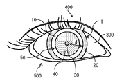
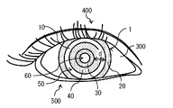
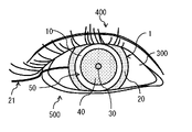
- FIG. 1 is a diagram showing an example of functional blocks of a receiving device provided in a contact lens according to an embodiment of the present disclosure
- FIG. 1. It is a figure showing an example of a state that the eye is mounted
- FIG. 3 is a diagram showing an example layout of circuit components of a receiving device provided in the contact lens of FIG. 2;
- FIG. 3 is a diagram showing an example layout of circuit components of a receiving device provided in the contact lens of FIG. 2;
- FIG. 4 is a diagram showing a modified example of the cross-sectional configuration of the contact lens of FIG. 3.
- FIG. 4 is a diagram showing a modified example of the cross-sectional configuration of the contact lens of FIG. 3.
- FIG. 4 is a diagram showing a modified example of the cross-sectional configuration of the contact lens of FIG. 3.
- FIG. 4 is a diagram showing a modified example of the cross-sectional configuration of the contact lens of FIG. 3.
- FIG. 4 is a diagram showing a modified example of the cross-sectional configuration of the contact lens of FIG. 3.
- FIG. 4 is a diagram showing a modified example of the cross-sectional configuration of the contact lens of FIG. 3.
- FIG. 4 is a diagram showing a modified example of the cross-sectional configuration of the contact lens of FIG. 3.
- FIG. 4 is a diagram showing a modified example of the cross-sectional configuration of the contact lens of FIG. 3.
- FIG. 4 is a diagram showing a modified example of the cross-sectional configuration of the contact
- FIG. 4 is a diagram showing a modified example of the cross-sectional configuration of the contact lens of FIG. 3.
- FIG. 4 is a diagram showing a modified example of the cross-sectional configuration of the contact lens of FIG. 3.
- FIG. 4 is a diagram representing a variation of the contact lens of FIG. 3;
- FIG. 4 is a diagram representing a variation of the contact lens of FIG. 3;
- FIG. 4 is a diagram representing a variation of the contact lens of FIG. 3;
- FIG. 4 is a diagram representing a variation of the contact lens of FIG. 3;
- FIG. 4 is a diagram representing a variation of the contact lens of FIG. 3;
- FIG. 4 is a diagram representing a variation of the contact lens of FIG. 3;
- FIG. 4 is a diagram showing a modification of the antenna element of FIG.
- FIG. 4 is a diagram showing a modification of the antenna element of FIG. 3;
- FIG. 4 is a diagram showing a modification of the antenna element of FIG. 3;
- 2 is a diagram illustrating an example of a schematic configuration of a power storage unit in FIG. 1;
- FIG. 2 is a diagram illustrating an example of a circuit configuration of a rectifier circuit in FIG. 1;
- FIG. FIG. 27 is a diagram for explaining the characteristics of the diode in FIG. 26;
- FIG. 3 is a diagram showing an example of a voltage waveform generated by a human body;
- FIG. 4 is a diagram showing an application example in which the present disclosure is applied to the operation of a notebook personal computer; It is a figure showing the example of a changed completely type of the circuit structure of the rectifier circuit of FIG. 2 is a diagram showing a configuration example for increasing the output of the receiver of FIG. 1; FIG. 2 is a diagram showing a configuration example for increasing the output of the receiver of FIG. 1; FIG. It is a figure showing the structural example which connected the rectifier circuit of FIG. 1 in series. 34 is a diagram showing a circuit configuration example of the rectifier circuit of FIG. 33; FIG. It is a figure showing the structural example which connected the rectifier circuit of FIG. 1 in series. 36 is a diagram showing a circuit configuration example of the rectifier circuit of FIG. 35; FIG.
- FIG. 38 is a diagram showing a circuit configuration example of the rectifier circuit of FIG. 37;
- FIG. It is a figure showing the structural example which connected the rectifier circuit of FIG. 1 in parallel.
- 40 is a diagram showing a circuit configuration example of the rectifier circuit of FIG. 39;
- FIG. 39 is a diagram showing a circuit configuration example of the rectifier circuit of FIG. 39;
- FIG. 1 shows an example of functional blocks of a receiving device 100 provided in a contact lens 1.
- FIG. 2 shows an example of how the contact lens 1 provided with the receiver 100 of FIG. 3 and 4 show an example layout of circuit components of the receiving device 100 provided in the contact lens 1 of FIG.
- the receiving device 100 has an antenna device 110 .
- Antenna device 110 has antenna section 111 and rectifier circuit 112 .
- the antenna unit 111 receives, for example, radio waves in space or electric field energy of a quasi-electrostatic field (near field) via the human body (eg, the upper eyelid 400 and the lower eyelid 500).
- the antenna unit 111 receives, for example, AC electrical energy output from a wearable device such as a wristwatch via the human body (eg, the upper eyelid 400 and the lower eyelid 500). In any case, the antenna unit 111 receives AC energy through the human body.
- the rectifier circuit 112 rectifies the alternating current energy received by the antenna section 111 and outputs the resulting direct current energy to the subsequent stage.
- radio waves There is a great amount of electric field energy around us, but it can be divided into low frequency components and high frequency components. For example, electric fields leaked from AC power supplies in homes, noise existing near personal computers, and voltages generated when people walk are low frequency components. These are called quasi-electrostatic fields.
- radio broadcasts, television broadcasts, mobile phone radio waves, etc. have high frequency components. These are called radio waves.
- the receiving device 100 further includes a charger section 120 and a power storage section 130 .
- Charger unit 120 outputs the DC energy input from rectifier circuit 112 to power storage unit 130 .
- Charger unit 120 may control discharge of DC energy accumulated in power storage unit 130 .
- Power storage unit 130 includes, for example, at least one of a capacitor and a battery that can temporarily store DC energy.
- Power storage unit 130 temporarily stores, for example, DC energy input from charger unit 120 .
- power storage unit 130 stores DC energy from charger unit 120 in the capacitor, and stores the energy that cannot be stored in the capacitor in the battery.
- load 200 is connected to power storage unit 130 .
- the load 200 includes, for example, a microcontroller, a wireless communication unit, sensors, and the like.
- the microcontroller controls the wireless communication unit, the sensor, and the like, and the output of the sensor is output to the outside via the wireless communication unit.
- the load 200 corresponds to a specific example of "load" of the present disclosure.
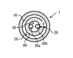
- the antenna section 111 has two antenna elements 20 and 30, for example, as shown in FIG.
- the antenna element 20 includes a conductor (hereinafter referred to as "first conductor") provided at a position in contact with the eyelid (at least one of the upper eyelid 400 and the lower eyelid 500) when the eye is open.
- the first conductor is in contact with the eyelid (at least one of the upper eyelid 400 and the lower eyelid 500) either directly or through some layer when the eye is open or when the eye is closed.
- the antenna element 20 receives the electric field energy of, for example, radio waves in space or a quasi-electrostatic field (near field) via the eyelid (at least one of the upper eyelid 400 and the lower eyelid 500) between the antenna element 30. .
- the antenna element 20 and the antenna element 30 for example, AC electrical energy output from a wearable device such as a wristwatch is received via the eyelid (at least one of the upper eyelid 400 and the lower eyelid 500).
- the antenna elements 20, 30 receive AC energy through the human body.
- the antenna element 30 is a conductor (hereinafter referred to as (referred to as a "second conductor").
- the second conductor is not in contact with the eyelids (upper eyelid 400 and lower eyelid 500) when the eyes are open, and contacts the eyelids (upper eyelid 400 and lower eyelid 500) directly or through some layer when the eyes are closed.
- the antenna element 30 is capacitively coupled with ground.
- the first conductor is, for example, a conductor such as gold, silver, aluminum, copper, iron, nickel, or an alloy, and has a plate shape, for example.
- the first conductor may be, for example, a conductive resin mixed with carbon, metal, or the like, or a material that conducts electricity, such as conductive rubber.
- the antenna element 20 may further have, for example, a resin coating layer covering the first conductor. The resin coating layer prevents corrosion of the first conductor due to contact with moisture such as tears.
- the second conductor is, for example, a conductor such as gold, silver, aluminum, copper, iron, nickel, or an alloy, and has a plate shape, for example.
- the second conductor may be, for example, a conductive resin mixed with carbon, metal, or the like, or a material that conducts electricity, such as conductive rubber.
- the circuit section 40 includes, for example, the circuit of the antenna device 110 excluding the two antenna elements 20 and 30, the charger section 120 and the power storage section .
- the circuit section 40 may also have a load 200, for example.
- a predetermined gap d exists between the first conductor and the second conductor in plan view. That is, the first conductor and the second conductor are arranged so as not to overlap each other in plan view. Further, for example, a gap 50 may exist between the circuit section 40 and the first conductor in plan view. That is, the circuit section 40 and the first conductor may be arranged so as not to overlap each other in plan view.
- the antenna element 30 may be provided, for example, within a circuit chip on which the circuit section 40 is formed.
- the shape of the antenna element 30 (second conductor) is not particularly limited.
- the antenna element 30 (second conductor) may have, for example, a circular shape as shown in FIG. 3, or may have an annular shape as shown in FIG. It may be C-shaped.
- the antenna element 30 may have, for example, a square shape, a polygonal shape, a square ring shape, or a polygonal ring shape.
- the gap d between the first conductor and the second conductor may be constant regardless of location, or may vary depending on location.
- the antenna element 30 (second conductor) is circular
- the antenna element 30 (second conductor) is preferably provided in the center of the lens substrate 10 .
- the antenna element 30 (second conductor) has an annular shape
- an opening 60 as shown in FIG. 4 is formed in the center of the antenna element 30 (second conductor).
- the antenna element 20 is preferably provided on the outer edge of the lens substrate 10, for example.
- FIG. 5 shows a cross-sectional configuration example of the contact lens 1 of FIG.
- FIG. 6 shows a cross-sectional configuration example of the contact lens 1 of FIG.
- the contact lens 1 is originally formed in an arc shape along the surface shape of the eyeball 300, but in FIGS. is expressed in a straight line.
- the contact lens 1 includes, for example, a lens substrate 10, and antenna elements 20 and 30 and a circuit portion 40 provided on the surface of the lens substrate 10 on the side of the upper eyelid 400, as shown in FIGS. ing.
- the lens substrate 10 is composed of, for example, a resin substrate having a curved shape along the surface of the pupil 310 and the iris 320 of the surface of the eyeball 300 .
- Resin materials used for the lens substrate 10 include, for example, methyl methacrylate (MMA), siloxanyl methacrylate (SMA), fluoromethacrylate F (FMA), hydroxyethyl methacrylate (HEMA), and N-vinylpyrrolidone (N-VP). , dimethylacrylamide (DMAA), glycerol methacrylate (GMA), silicone rubber, butyl acrylate, dimethylsiloxane, collagen, amino acid copolymers, and the like.
- MMA methyl methacrylate
- SMA siloxanyl methacryl
- the antenna element 30 and the circuit section 40 may be provided on the surface of the lens substrate 10 on the eyeball 300 side (the back surface of the lens substrate 10), as shown in FIG. At this time, an opening 51 is formed in the antenna element 20 at a location facing the antenna element 30 and the circuit section 40 .
- the antenna element 30 (second conductor) is covered with, for example, the circuit section 40, and the circuit section 40 prevents the antenna element 30 (second conductor) from coming into contact with moisture such as tears.
- the circuit section 40 has a thickness that allows isolation from the human body.
- the circuit section 40 may include an insulating material such as resin, or the surface of the circuit section 40 may be covered with an insulating layer made of resin or the like.
- the antenna element 30 (second conductor) may be covered with a resin or the like that is separate from the circuit section 40, for example. In FIG. 7, the portion of the lens substrate 10 corresponding to the antenna element 30 may be a conductor.
- the antenna element 30 may be arranged inside the lens substrate 10, for example, as shown in FIG.
- the circuit section 40 may be arranged on the surface of the lens substrate 10 as shown in FIG. 8, or may be arranged inside the lens substrate 10 .
- the antenna element 30 and the circuit section 40 may be covered with an insulating layer 70, for example, as shown in FIG.
- the insulating layer 70 is formed, for example, so as to fill the opening 51 of the antenna element 20, and is made of, for example, resin.
- the antenna element 30 and the circuit section 40 may be covered with a water-repellent layer 71 that is water-repellent to water such as tears.
- the water-repellent layer 71 is made of a material containing functional groups such as saturated fluoroalkyl groups (especially trifluoromethyl groups CF3-), alkylsilyl groups, fluorosilyl groups, and long-chain alkyl groups.
- the antenna element 30 and the circuit section 40 may be covered with a hydrophobic layer 72 that is hydrophobic to moisture such as tears.
- the hydrophobic layer 72 is made of, for example, a lipophilic material, silicone, a compound having a fluoroalkyl chain, or the like.
- the surfaces of the antenna element 30 and the circuit section 40 may be subjected to water-repellent treatment (for example, plasma treatment).
- the height of the antenna element 30 (second conductor) from the surface of the lens substrate 10 is the height of the antenna element 20 (first conductor) from the surface of the lens substrate 10, as shown in FIG. It may be taller than the height. In this case, it is possible to prevent the surface of the antenna element 30 (second conductor) from being covered with moisture such as tears.
- the antenna element 30 may be covered with a water-repellent layer 31 that repels water such as tears.
- the antenna element 30 and the circuit section 40 may be covered with a hydrophobic layer 32 that is hydrophobic to moisture such as tears.
- the water-repellent layer 31 has the same structure as the water-repellent layer 71, for example.
- the hydrophobic layer 32 has the same configuration as the hydrophobic layer 72, for example.
- a water-repellent structure may be formed by water-repellent treatment.
- a hydrophobic structure may be formed on the surface of the antenna element 30 (second conductor) by hydrophobic treatment, for example, as shown in FIG.
- the water-repellent structure or hydrophobic structure includes, for example, a lotus leaf structure.
- the lotus leaf structure is composed of, for example, an uneven surface on which fine projections of ⁇ m order are arranged. On this uneven surface, each protrusion has a large number of nano-sized protrusions.
- the first conductor of the antenna element 20 is provided on the lens substrate 10 at a position in contact with the eyeball or eyelid when the eye is open.
- the second conductor of the antenna element 30 is provided on the lens substrate 10 at a position separated from the first conductor by a predetermined gap and not in contact with the eyeball or eyelids when the eyes are open.
- the electric field energy of radio waves or quasi-electrostatic fields (near field) in space can be received via the eyeballs or eyelids.
- AC electrical energy output from a wearable device such as a wristwatch can be received via the eyeball or eyelid.
- the contact lens 1 can receive sufficient power.
- the first conductor is provided on the outer edge of the lens substrate 10 . This ensures that the first conductor is brought into contact with the eyeball or eyelid. As a result, it is possible to provide the contact lens 1 with high antenna performance.
- the second conductor is provided in the center of the lens substrate 10 or in an annular region around the center of the lens substrate 10 .
- the gap d can be reliably provided between the first conductor and the second conductor.
- the first conductor is provided on the eyelid-side surface of the lens substrate 10 . Thereby, the first conductor can be reliably brought into contact with the eyelid.
- the second conductor is provided on the surface of the lens substrate 10 on the eyelid side or the surface opposite to the eyelid, or on the inside of the lens substrate 10 . This makes it possible to ensure capacitive coupling between the second conductor and the ground.
- an insulating layer 70, a water-repellent layer 71, a hydrophobic layer 72, a water-repellent layer 31, or a hydrophobic layer 32 are provided to cover the second conductor, or the surface of the second conductor is subjected to water-repellent treatment or hydrophobic treatment.
- the surface of the second conductor is treated or has a water-repellent structure or a hydrophobic structure. This can prevent the surface of the second conductor from coming into direct contact with moisture such as tears.
- the second antenna element (second conductor) can form a pseudo ground through capacitive coupling with the ground.
- the height of the antenna element 30 (second conductor) from the surface of the lens substrate 10 is higher than the height of the antenna element 20 (first conductor) from the surface of the lens substrate 10. It's becoming This makes it difficult for the surface of the antenna element 30 (second conductor) to be covered with moisture such as tears. As a result, the antenna element 30 (second conductor) can form a pseudo ground through capacitive coupling with the ground.
- a rectifier circuit 112 is provided in this embodiment. This makes it possible to store the DC energy generated by the rectifier circuit 112 in the storage unit 130 and supply the DC energy stored in the storage unit 130 to the load 200 .
- a capacitor is provided to store the DC signal obtained by rectification in the rectifier circuit 112 . This makes it possible to supply the DC energy accumulated in the capacitor to the load 200 .
- antenna element 20 may have a conductor provided at a position in contact with eyeball 300 .
- the antenna element 20 may have a conductor provided on the back surface of the lens substrate 10 (the surface on the eyeball 300 side), as shown in FIGS. 14 and 15, for example.
- the conductor is made of, for example, the same material as the first conductor.
- the conductor may be provided on the outer edge portion of the back surface of the lens substrate 10 .
- the conductor may be provided in the central portion of the rear surface of the lens substrate 10 as shown in FIG. 14 and 15 omit the description of the configuration other than the lens substrate 10 and the antenna element 20.
- FIG. 14 and 15 omit the description of the configuration other than the lens substrate 10 and the antenna element 20.
- the antenna element 30 may be provided on the upper surface of the lens substrate 10 at a position that does not come into contact with the eyelid when the eye is open. This is because the antenna element 20 is provided on the rear surface of the lens substrate 10 and is not located at a position that hinders capacitive coupling between the antenna element 30 and the ground.
- the antenna element 20 receives, for example, radio waves or electric field energy of a quasi-electrostatic field (near field) in space via the eyeball 300 .
- the antenna element 20 receives, via the eyeball 300, alternating current electrical energy output from a wearable device such as a wristwatch.
- the antenna element 20 receives AC energy through the human body.
- the antenna element 20 acquires electric field energy through the eyeball 300 .
- the contact lens 1 can receive sufficient power.
- the antenna element 20 may have, for example, an extraction electrode 21 in contact with a conductor in contact with the upper eyelid 400, the lower eyelid 500, or the eyeball 300, as shown in FIG. .
- the extraction electrode 21 is a wiring electrode that can reach from the surface of the lens substrate 10 to the surface of the face, and is in contact with the surface of the face.
- the electric field energy of radio waves or quasi-electrostatic fields (near field) in the space can be received via the extraction electrode 21.
- alternating current electrical energy output from a wearable device such as a wristwatch can be received via the extraction electrode 21 .
- the contact lens 1 can receive sufficient power.
- the antenna element 30 may be divided into a plurality of parts as shown in FIGS. 17, 18 and 19, for example.
- the two elements 30a and 30b may be connected to a common rectifier circuit 112 or It may be connected to different rectifier circuits 112 .
- the shape of the two elements 30a and 30b is not particularly limited, but may be, for example, a hemispherical shape as shown in FIG. 18, or a circular shape as shown in FIG. It may have a shape. A case where the two elements 30a and 30b are connected to different rectifier circuits 112 will be described in detail later.
- the antenna element 20 may be divided into a plurality of parts as shown in FIGS. 20 and 21, for example.
- the two elements 20a and 20b may be connected to a common rectifier circuit 112 or It may be connected to different rectifier circuits 112 .
- the shape of the two elements 20a and 20b is not particularly limited, but may be hemispherical as shown in FIG. 20, or circular as shown in FIG. It may have a shape. A case where the two elements 20a and 20b are connected to different rectifier circuits 112 will be described in detail later.
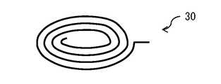
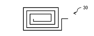
- the antenna element 30 may have a spiral shape as shown in FIGS. 22 and 23, for example.
- the antenna element 30 may have a single-layer spiral shape, or may have a multi-layer spiral shape.
- the spiral shape of the antenna element 30 is not particularly limited, but may be, for example, an annular spiral shape without corners as shown in FIG. It may have a quadrangular annular spiral shape as shown in FIG.
- the antenna element 30 may have a meandering shape (rectangular wave shape) as shown in FIG. 24, for example.
- the storage unit 130 may include capacitors 130a connected in series, for example, as shown in FIG. 25(A). At this time, the storage unit 130 further includes a circuit that connects in series only one or a plurality of capacitors 130a that are not out of order among the plurality of capacitors 130a when, for example, some of the capacitors 130a are faulty. may be composed of Further, in the above-described embodiment and its modification, power storage unit 130 may be C-shaped, for example, as shown in FIG. 25(B).
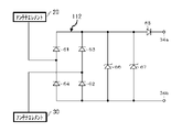
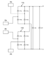
- the rectifier circuit 112 includes, for example, four diodes 61 to 64 as shown in FIG. 67 (eg, Zener voltage is 6.5V).
- the diodes 61 and 64 are connected in series with each other, and the diodes 63 and 62 are connected in series with each other.
- a connection point between the anode of diode 61 and the cathode of diode 64 is connected to antenna element 20
- a connection point between the anode of diode 63 and the cathode of diode 62 is connected to antenna element 30 .
- a connection point of the cathode of the diode 61 and the cathode of the diode 63 is connected to one output terminal 34a via a backflow prevention diode 65, and a connection point of the anode of the diode 64 and the anode of the diode 62 is connected to the other output terminal 34b.
- a varistor 66 for electrostatic countermeasures and a Zener diode 67 for IC protection are connected in parallel between the output terminals 34a and 34b.
- the four diodes 61 to 64 may be configured discretely or may be configured with a dedicated IC.
- FIG. 27 shows the results of measuring the forward voltage Vf and the reverse current Is of the four diodes 61 to 64 used in the rectifier circuit 112.
- FIG. 27 As the diode product number 1N60, silicon and germanium diodes were measured, and another product number ISS108 was evaluated using a germanium diode manufactured by a different manufacturer.
- curve 42 is the characteristic of 1N60 (silicon)
- curve 41 is the characteristic of 1N60 (germanium)
- curve 43 is the characteristic of ISS108 (germanium).
- a reverse current Is is a current that flows when a voltage is applied to the four diodes 61 to 64 in the reverse direction.
- the measurement data in Table 1 are data when 10 V is applied in the reverse direction of the diode.
- the forward voltage Vf is the voltage when the forward current (1 mA) begins to flow through the diode.
- the diode 1N60 (silicon) in which the current does not flow in the reverse direction can take in more power than the diode with a low voltage at which the current starts to flow in the forward direction. Do you get it. Since the rectified input is alternating current, the reverse current Is when the forward voltage Vf of the diodes 61 to 64 is applied in the reverse direction is 10 V in Table 1, so the same voltage as Vf is applied in the reverse direction. The reverse current Is when applied is calculated to be 0.036 ⁇ A for 1N60 (silicon), 0.21 ⁇ A for 1N60 (germanium) and 0.5 ⁇ A for ISS108 (germanium).
- the ratio of forward current (1 mA)/reverse current Is is calculated to be 1/27778 for 1N60 (silicon), 1/4762 for 1N60 (germanium), and 2000 for ISS108 (germanium). 1/1.
- the diodes 61 to 64 used in the rectifier circuit 112 should have the above ratio of about 4700 times or more, preferably 10000 or more.
- 1N60 (silicon) has the most suitable characteristics.
- the reverse current Is when applied in the reverse direction should be small.
- 1N60 (germanium) is 1.43 M ⁇ and ISS108 (germanium) is 0.38 M ⁇ .
- the resistance value that prevents the current from flowing in the reverse direction should be large.
- it is 10 M ⁇ or more.
- 1N60 (silicon) has the most suitable characteristics.
- the antenna elements 20 and 30 may receive an electric field generated as a person walks. At this time, the outputs of the antenna elements 20 and 30 have voltage waveforms as shown in FIG. 28, for example. In this way, the receiving device 100 captures the electric field generated by human walking as energy, so that the contact lens 1 can receive sufficient power even in a place with little external noise, for example. can.
- the energy taken in by the receiving device 100 may be power or noise leaking from the notebook personal computer 44 .
- the antenna is the human body, and the ground of the receiving device 100 or a separate conductor creates an electric field, so that the frequency that can be received is not restricted by the shape of the antenna.
- the ground of the receiving device 100 or a separate conductor is capacitively coupled with the ground of the earth, it is possible to capture electric field energy in a quasi-electrostatic field other than radio waves. In other words, it is possible to convert power and noise leaking from power cords and inverters into energy.
- the human body is treated as a conductor, and power induced in the human body itself can be taken in between the receiving device 100 and the ground.
- the contact lens 1 having the receiving device 100 is attached to the eyeball 300 of the operator.
- the notebook personal computer 44 has a keyboard 45 made of resin, and electronic components such as a circuit board, a processor, and a switching power supply are provided directly below the keyboard 45 .
- Electronic components generate spatial noise 46 as indicated by arrows in FIG. 29, for example.
- the operator is spatially coupled with the electronic components mounted on the notebook personal computer 44 via a keyboard 45 made of resin. Therefore, when the operator operates the keyboard 45, the operator contacts the keyboard 45, and the receiving device 100 receives the spatial noise 46 emitted from the electronic component via the operator. For example, if the receiver 100 has a full-wave rectifier circuit and a capacitor (for example, 1.2 ⁇ F) is connected after the full-wave rectifier circuit, the terminal voltage of the capacitor rises to 1.2 V in 20 seconds.
- a capacitor for example, 1.2 ⁇ F
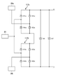
- the rectifier circuit 112 further includes a high-resistance (2 M ⁇ or more, preferably 10 M ⁇ ) voltmeter 81 for measuring the output voltage of the full-wave rectifier circuit, for example, as shown in FIG. may Furthermore, the rectifier circuit 112 may further include a battery 82 for charging the output of the full-wave rectifier circuit output via the anti-backflow diode 65, for example, as shown in FIG. At this time, the output of battery 82 may be used as the power source for voltmeter 81 .
- the output of the voltmeter 81 is analyzed by a computer or the like. At this time, the number or frequency of blinking can be detected based on the output of the voltmeter 81, for example. Whether or not the person has blinked can be determined, for example, by determining whether or not the antenna element 20 and the antenna element 30 are short-circuited.
- the person can be authenticated. Also, by collating the output of the voltmeter 81 with data of voltage fluctuations according to various physical conditions of the person, it is possible to estimate the physical condition of the person.
- a plurality of antenna devices 110 may be connected in series as shown in FIG. 31, for example. At this time, the voltage VL applied to the load 200 is the sum of the outputs of the antenna devices 110 (V1+V2+V3). Moreover, in the above embodiments and modifications thereof, a plurality of antenna devices 110 may be connected in parallel as shown in FIG. 32, for example. At this time, the current IL flowing through the load 200 is the sum of the outputs of the antenna devices 110 (I1+I2+I3).
- FIG. 33 shows an embodiment for increasing the output voltage of the antenna device 110.
- FIG. An antenna element 20 that contacts the human body is provided, and two antenna elements 30 (30a, 30b) are provided for the antenna element 20.
- FIG. A rectifying circuit 112 (112a) is provided for rectifying the output of the antenna section including the antenna elements 20 and 30a
- a rectifying circuit 112 (112b) is provided for rectifying the output of the antenna section including the antenna elements 20 and 30b.
- Rectifier circuits 112 a and 112 b are connected in series with each other, and outputs of the rectifier circuits 112 a and 112 b connected in series with each other are input to charger section 120 .
- FIG. 34 shows a circuit configuration example of the antenna device 110 of FIG.
- a full-wave rectifier circuit is used as the rectifier circuits 112a and 112b connected in series with each other.
- Zener diodes 66 and 67 are common elements for rectifier circuits 112a and 112b. By doing so, an output voltage of 8V can be obtained when an output voltage of 4V is obtained by one antenna device 110, for example.
- a larger output voltage can be obtained by connecting a plurality of (two or more) rectifier circuits 112 in series. Note that when the frequency of power supply noise or the like that induces voltage is low, there is no need to consider the distance between the antennas, so the configuration shown in this modified example is suitable.
- FIG. 35 shows an embodiment for increasing the output voltage of the antenna device 110.
- FIG. Two antenna elements 20a and 20b that are independent of each other are provided as the antenna element 20 that contacts the human body. Furthermore, two antenna elements 30a and 30b independent of each other are provided as the antenna element 30 capacitively coupled with the ground.
- a rectifying circuit 112 (112a) is provided for rectifying the output of the antenna section including the antenna elements 20a and 30a
- a rectifying circuit 112 (112b) is provided for rectifying the output of the antenna section including the antenna elements 20b and 30b.
- Rectifier circuits 112 a and 112 b are connected in series with each other, and outputs of the rectifier circuits 112 a and 112 b connected in series with each other are input to charger section 120 .
- FIG. 36 shows a configuration example of an antenna device 110 having rectifier circuits 112a and 112b arranged in series with each other.
- Zener diodes 66 and 67 are common elements for rectifier circuits 112a and 112b. By doing so, an output voltage of 8V can be obtained when an output voltage of 4V is obtained by one antenna device 110, for example. As described above, a larger output voltage can be obtained by connecting a plurality of (two or more) rectifier circuits 112 in series. Note that when the frequency of power supply noise or the like that induces voltage is low, there is no need to consider the distance between the antennas, so the configuration shown in this modified example is suitable.
- the antenna element 20 is connected to the connection point between the diodes 61a and 64a and the connection point between the diodes 61b and 64b, respectively, in order to have the same phase in the rectifier circuits 112a and 112b.
- antenna elements 20a and 20b are connected to the connection point of diode 61a and diode 64a and the connection point of diode 61b and diode 64b, respectively, in order to have the same phase in rectifier circuits 112a and 112b. Connected.
- FIG. 37 shows an embodiment for increasing the output current of the antenna device 110.
- FIG. An antenna element 20 that contacts the human body is provided, and two antenna elements 30 (30a, 30b) are provided for the antenna element 20.
- FIG. A rectifying circuit 112 (112a) is provided for rectifying the output of the antenna section including the antenna elements 20 and 30a
- a rectifying circuit 112 (112b) is provided for rectifying the output of the antenna section including the antenna elements 20 and 30b.
- Rectifying circuits 112 a and 112 b are connected in parallel, and the outputs of rectifying circuits 112 a and 112 b connected in parallel are input to charger section 120 .
- FIG. 38 shows a circuit configuration example of the antenna device 110 of FIG.
- a full-wave rectifier circuit is used as the rectifier circuits 112a and 112b connected in parallel with each other.
- Zener diodes 66 and 67 are common elements for rectifier circuits 112a and 112b.
- FIG. 39 shows an example for increasing the output current of the antenna device 110.
- FIG. Two antenna elements 20a and 20b that are independent of each other are provided as the antenna element 20 that contacts the human body. Further, two antenna elements 30a and 30b that contact different parts of the human body are provided as the antenna element 30 that is capacitively coupled with the ground.
- a rectifying circuit 112 (112a) is provided for rectifying the output of the antenna section including the antenna elements 20a and 30a, and a rectifying circuit 112 (112b) is provided for rectifying the output of the antenna section including the antenna elements 20b and 30b. Rectifying circuits 112 a and 112 b are connected in parallel, and the outputs of rectifying circuits 112 a and 112 b connected in parallel are input to charger section 120 .
- FIG. 40 shows a configuration example of an antenna device 110 having rectifier circuits 112a and 112b arranged in parallel with each other.
- Zener diodes 66 and 67 are common elements for rectifier circuits 112a and 112b.
- an output current of 1 ⁇ A for example, an output current of 2 ⁇ A can be obtained.
- a larger output current can be obtained by connecting a plurality of (two or more) rectifier circuits 112 in parallel. Note that when the frequency of power supply noise or the like that induces voltage is low, there is no need to consider the distance between the antennas, so the configuration shown in this modified example is suitable.
- series connection of a plurality of rectifier circuits 112 and parallel connection of a plurality of rectifier circuits 112 may be appropriately combined according to the required voltage and current to be induced.
- the present disclosure can have the following configurations.
- the antenna section a first antenna element including a first conductor provided at a position in contact with the eyeball or the eyelid when the eye is open; and a second antenna element including a second conductor provided at a position separated from the first conductor by a predetermined gap and not in contact with the eyeball or the eyelid when the eye is open.
- the first antenna element further has an extraction electrode in contact with the first conductor,
- the contact lens according to (8), wherein the second conductor is provided on the surface of the lens substrate opposite to the eyelid.
- the first antenna element further has an extraction electrode in contact with the first conductor,
- any one of (1) to (5), wherein the height of the second conductor from the surface of the lens substrate is higher than the height of the first conductor from the surface of the lens substrate Contact lenses according to one.
- the first conductor of the first antenna element is provided on the lens substrate at a position in contact with the eyeball or eyelid when the eye is open.
- the second conductor of the second antenna element is provided on the lens substrate at a position with a predetermined gap from the first conductor and not in contact with the eyeball or eyelids when the eyes are open.
- the electric field energy of radio waves or quasi-electrostatic fields (near field) in space can be received via the eyeballs or eyelids.
- AC electrical energy output from a wearable device such as a wristwatch can be received via the eyeball or eyelid.
- the contact lens can receive sufficient power.
Landscapes
- Physics & Mathematics (AREA)
- Health & Medical Sciences (AREA)
- Ophthalmology & Optometry (AREA)
- General Health & Medical Sciences (AREA)
- General Physics & Mathematics (AREA)
- Optics & Photonics (AREA)
- Engineering & Computer Science (AREA)
- Otolaryngology (AREA)
- Acoustics & Sound (AREA)
- Computer Networks & Wireless Communication (AREA)
- Power Engineering (AREA)
- Aerials With Secondary Devices (AREA)
- Details Of Aerials (AREA)
- Near-Field Transmission Systems (AREA)
Priority Applications (3)
| Application Number | Priority Date | Filing Date | Title |
|---|---|---|---|
| JP2023533084A JPWO2023281835A1 (https=) | 2021-07-05 | 2022-03-16 | |
| KR1020247003751A KR20240022666A (ko) | 2021-07-05 | 2022-03-16 | 콘택트 렌즈 |
| US18/574,343 US20240295758A1 (en) | 2021-07-05 | 2022-03-16 | Contact lens |
Applications Claiming Priority (2)
| Application Number | Priority Date | Filing Date | Title |
|---|---|---|---|
| JP2021111775 | 2021-07-05 | ||
| JP2021-111775 | 2021-07-05 |
Publications (1)
| Publication Number | Publication Date |
|---|---|
| WO2023281835A1 true WO2023281835A1 (ja) | 2023-01-12 |
Family
ID=84801384
Family Applications (1)
| Application Number | Title | Priority Date | Filing Date |
|---|---|---|---|
| PCT/JP2022/011864 Ceased WO2023281835A1 (ja) | 2021-07-05 | 2022-03-16 | コンタクトレンズ |
Country Status (4)
| Country | Link |
|---|---|
| US (1) | US20240295758A1 (https=) |
| JP (1) | JPWO2023281835A1 (https=) |
| KR (1) | KR20240022666A (https=) |
| WO (1) | WO2023281835A1 (https=) |
Citations (2)
| Publication number | Priority date | Publication date | Assignee | Title |
|---|---|---|---|---|
| WO2016067433A1 (ja) * | 2014-10-30 | 2016-05-06 | 株式会社ニコン | レンズシステム及びコンタクトレンズ |
| JP2018534606A (ja) * | 2015-09-16 | 2018-11-22 | イー−ビジョン スマート オプティックス, インク.E−Vision Smart Optics, Inc. | ワイヤレス充電を用いる眼用レンズのためのシステム、装置、及び方法 |
Family Cites Families (6)
| Publication number | Priority date | Publication date | Assignee | Title |
|---|---|---|---|---|
| ES2332203T3 (es) * | 1996-05-31 | 2010-01-28 | Toto Ltd. | Elemento antiincrustante y composicion de revestimiento antiincrustante. |
| KR20030088005A (ko) | 2003-10-17 | 2003-11-15 | 장시영 | 표결에서 자신의 선택을 확인하는 전자식 무선표결시스템 |
| US8857983B2 (en) * | 2012-01-26 | 2014-10-14 | Johnson & Johnson Vision Care, Inc. | Ophthalmic lens assembly having an integrated antenna structure |
| US20170358841A1 (en) * | 2014-10-21 | 2017-12-14 | Medella Health Inc. | Multi-layer micro receiver for a wireless communication system |
| US11137622B2 (en) * | 2018-07-15 | 2021-10-05 | Tectus Corporation | Eye-mounted displays including embedded conductive coils |
| JP2020016812A (ja) * | 2018-07-27 | 2020-01-30 | 真一 芦田 | 眼用器具 |
-
2022
- 2022-03-16 JP JP2023533084A patent/JPWO2023281835A1/ja active Pending
- 2022-03-16 KR KR1020247003751A patent/KR20240022666A/ko not_active Withdrawn
- 2022-03-16 WO PCT/JP2022/011864 patent/WO2023281835A1/ja not_active Ceased
- 2022-03-16 US US18/574,343 patent/US20240295758A1/en active Pending
Patent Citations (2)
| Publication number | Priority date | Publication date | Assignee | Title |
|---|---|---|---|---|
| WO2016067433A1 (ja) * | 2014-10-30 | 2016-05-06 | 株式会社ニコン | レンズシステム及びコンタクトレンズ |
| JP2018534606A (ja) * | 2015-09-16 | 2018-11-22 | イー−ビジョン スマート オプティックス, インク.E−Vision Smart Optics, Inc. | ワイヤレス充電を用いる眼用レンズのためのシステム、装置、及び方法 |
Also Published As
| Publication number | Publication date |
|---|---|
| KR20240022666A (ko) | 2024-02-20 |
| US20240295758A1 (en) | 2024-09-05 |
| JPWO2023281835A1 (https=) | 2023-01-12 |
Similar Documents
| Publication | Publication Date | Title |
|---|---|---|
| JP3905418B2 (ja) | 電源装置および電子機器 | |
| Li et al. | Body-area powering with human body-coupled power transmission and energy harvesting ICs | |
| US20100001683A1 (en) | Charging apparatus, portable electronic device using the apparatus, and charging method thereof | |
| JP7666968B2 (ja) | 電力送信機、電力送受信装置、人体通信装置、及び電力送受信システム | |
| US20230155692A1 (en) | Method and device for energy transfer and harvesting | |
| US20190058271A1 (en) | Clip-type contactor and protective apparatus including same | |
| WO2017039928A1 (en) | Apparatus, system and method for photodetection with a transimpedance amplifier of an eye-mountable device | |
| US9209324B2 (en) | Photovoltaic cell arrangements | |
| Nguyen et al. | Powering smart jewelry using an RF energy harvesting necklace | |
| US20230299465A1 (en) | Antenna device, rectifier circuit, power supply device, and electronic device | |
| WO2023281835A1 (ja) | コンタクトレンズ | |
| US11076946B2 (en) | Flexible barrier layer including superelastic alloys | |
| WO2023106004A1 (ja) | 整流回路及び発電装置 | |
| Hsieh et al. | An RF energy harvester with 35.7% PCE at P IN of− 15 dBm | |
| WO2023127284A1 (ja) | アンテナ装置および電子機器 | |
| EP4380004A1 (en) | Charging device | |
| KR102953326B1 (ko) | 안테나 장치, 정류 회로, 전원 장치 및 전자 기기 | |
| KR20230011105A (ko) | 무선 충전용 그립톡 | |
| US20240422467A1 (en) | Electronic device | |
| JP2015192687A (ja) | 発光装置及び付け爪 | |
| CN120767955A (zh) | 充电底座、电子设备、充电控制方法和充电系统 | |
| KR20260060671A (ko) | 에너지 하베스팅 웨어러블 밴드 | |
| Ohmura et al. | Development of Zero Powered Human Detection Sensor Using Environmental Electric Noise | |
| CN118541631A (zh) | 包括天线的可穿戴电子设备 | |
| HK1140319A1 (en) | Power adapter for impedance stabilization |
Legal Events
| Date | Code | Title | Description |
|---|---|---|---|
| 121 | Ep: the epo has been informed by wipo that ep was designated in this application |
Ref document number: 22837257 Country of ref document: EP Kind code of ref document: A1 |
|
| WWE | Wipo information: entry into national phase |
Ref document number: 2023533084 Country of ref document: JP |
|
| ENP | Entry into the national phase |
Ref document number: 20247003751 Country of ref document: KR Kind code of ref document: A |
|
| NENP | Non-entry into the national phase |
Ref country code: DE |
|
| 122 | Ep: pct application non-entry in european phase |
Ref document number: 22837257 Country of ref document: EP Kind code of ref document: A1 |