WO2023281795A1 - Protection circuit and semiconductor device - Google Patents
Protection circuit and semiconductor device Download PDFInfo
- Publication number
- WO2023281795A1 WO2023281795A1 PCT/JP2022/005953 JP2022005953W WO2023281795A1 WO 2023281795 A1 WO2023281795 A1 WO 2023281795A1 JP 2022005953 W JP2022005953 W JP 2022005953W WO 2023281795 A1 WO2023281795 A1 WO 2023281795A1
- Authority
- WO
- WIPO (PCT)
- Prior art keywords
- semiconductor device
- misfet
- protection circuit
- external terminal
- main electrode
- Prior art date
Links
- 239000004065 semiconductor Substances 0.000 title claims description 255
- 239000000969 carrier Substances 0.000 claims abstract description 60
- 230000005669 field effect Effects 0.000 claims abstract description 38
- 238000003860 storage Methods 0.000 claims description 39
- 239000000758 substrate Substances 0.000 claims description 31
- 239000003990 capacitor Substances 0.000 claims description 22
- 230000008878 coupling Effects 0.000 claims description 16
- 238000010168 coupling process Methods 0.000 claims description 16
- 238000005859 coupling reaction Methods 0.000 claims description 16
- 150000004767 nitrides Chemical class 0.000 claims description 16
- 150000001875 compounds Chemical class 0.000 claims description 8
- 229910001218 Gallium arsenide Inorganic materials 0.000 claims description 3
- VYPSYNLAJGMNEJ-UHFFFAOYSA-N Silicium dioxide Chemical compound O=[Si]=O VYPSYNLAJGMNEJ-UHFFFAOYSA-N 0.000 claims 4
- PNEYBMLMFCGWSK-UHFFFAOYSA-N aluminium oxide Inorganic materials [O-2].[O-2].[O-2].[Al+3].[Al+3] PNEYBMLMFCGWSK-UHFFFAOYSA-N 0.000 claims 3
- 229910052593 corundum Inorganic materials 0.000 claims 3
- CJNBYAVZURUTKZ-UHFFFAOYSA-N hafnium(IV) oxide Inorganic materials O=[Hf]=O CJNBYAVZURUTKZ-UHFFFAOYSA-N 0.000 claims 3
- 229910001845 yogo sapphire Inorganic materials 0.000 claims 3
- MCMNRKCIXSYSNV-UHFFFAOYSA-N Zirconium dioxide Chemical compound O=[Zr]=O MCMNRKCIXSYSNV-UHFFFAOYSA-N 0.000 claims 2
- 229910052681 coesite Inorganic materials 0.000 claims 2
- 229910052906 cristobalite Inorganic materials 0.000 claims 2
- 239000000377 silicon dioxide Substances 0.000 claims 2
- 235000012239 silicon dioxide Nutrition 0.000 claims 2
- 229910052682 stishovite Inorganic materials 0.000 claims 2
- 229910052905 tridymite Inorganic materials 0.000 claims 2
- PBCFLUZVCVVTBY-UHFFFAOYSA-N tantalum pentoxide Inorganic materials O=[Ta](=O)O[Ta](=O)=O PBCFLUZVCVVTBY-UHFFFAOYSA-N 0.000 claims 1
- RUDFQVOCFDJEEF-UHFFFAOYSA-N yttrium(III) oxide Inorganic materials [O-2].[O-2].[O-2].[Y+3].[Y+3] RUDFQVOCFDJEEF-UHFFFAOYSA-N 0.000 claims 1
- 238000009825 accumulation Methods 0.000 abstract description 20
- 230000000694 effects Effects 0.000 description 33
- 238000000034 method Methods 0.000 description 32
- 238000005516 engineering process Methods 0.000 description 21
- 238000004519 manufacturing process Methods 0.000 description 19
- 238000002347 injection Methods 0.000 description 17
- 239000007924 injection Substances 0.000 description 17
- 230000008569 process Effects 0.000 description 17
- 230000004044 response Effects 0.000 description 14
- 230000006698 induction Effects 0.000 description 13
- 238000010586 diagram Methods 0.000 description 12
- 230000015572 biosynthetic process Effects 0.000 description 10
- 230000015556 catabolic process Effects 0.000 description 10
- 230000001681 protective effect Effects 0.000 description 10
- 229910018072 Al 2 O 3 Inorganic materials 0.000 description 9
- 239000012212 insulator Substances 0.000 description 9
- 230000004048 modification Effects 0.000 description 9
- 238000012986 modification Methods 0.000 description 9
- 238000002955 isolation Methods 0.000 description 7
- 229910004298 SiO 2 Inorganic materials 0.000 description 6
- 150000002500 ions Chemical class 0.000 description 5
- 239000000463 material Substances 0.000 description 4
- 229910002704 AlGaN Inorganic materials 0.000 description 3
- 239000007772 electrode material Substances 0.000 description 3
- 238000005530 etching Methods 0.000 description 3
- 238000005468 ion implantation Methods 0.000 description 3
- 230000002301 combined effect Effects 0.000 description 2
- 230000006378 damage Effects 0.000 description 2
- 238000009792 diffusion process Methods 0.000 description 2
- 238000009413 insulation Methods 0.000 description 2
- 230000003068 static effect Effects 0.000 description 2
- 230000001052 transient effect Effects 0.000 description 2
- 230000001133 acceleration Effects 0.000 description 1
- 230000004913 activation Effects 0.000 description 1
- 238000000231 atomic layer deposition Methods 0.000 description 1
- 239000000919 ceramic Substances 0.000 description 1
- 239000011195 cermet Substances 0.000 description 1
- 238000013461 design Methods 0.000 description 1
- 230000005684 electric field Effects 0.000 description 1
- 230000005611 electricity Effects 0.000 description 1
- 238000010438 heat treatment Methods 0.000 description 1
- 239000002784 hot electron Substances 0.000 description 1
- 239000012535 impurity Substances 0.000 description 1
- 238000007689 inspection Methods 0.000 description 1
- 238000010030 laminating Methods 0.000 description 1
- 238000005259 measurement Methods 0.000 description 1
- 238000000206 photolithography Methods 0.000 description 1
- 230000010287 polarization Effects 0.000 description 1
- 238000012545 processing Methods 0.000 description 1
- 230000002441 reversible effect Effects 0.000 description 1
- 229910052594 sapphire Inorganic materials 0.000 description 1
- 239000010980 sapphire Substances 0.000 description 1
- 229910000679 solder Inorganic materials 0.000 description 1
- 230000002269 spontaneous effect Effects 0.000 description 1
- 230000005533 two-dimensional electron gas Effects 0.000 description 1
- 238000001771 vacuum deposition Methods 0.000 description 1
Images


Classifications
-
- H—ELECTRICITY
- H01—ELECTRIC ELEMENTS
- H01L—SEMICONDUCTOR DEVICES NOT COVERED BY CLASS H10
- H01L21/00—Processes or apparatus adapted for the manufacture or treatment of semiconductor or solid state devices or of parts thereof
- H01L21/70—Manufacture or treatment of devices consisting of a plurality of solid state components formed in or on a common substrate or of parts thereof; Manufacture of integrated circuit devices or of parts thereof
- H01L21/77—Manufacture or treatment of devices consisting of a plurality of solid state components or integrated circuits formed in, or on, a common substrate
- H01L21/78—Manufacture or treatment of devices consisting of a plurality of solid state components or integrated circuits formed in, or on, a common substrate with subsequent division of the substrate into plural individual devices
- H01L21/82—Manufacture or treatment of devices consisting of a plurality of solid state components or integrated circuits formed in, or on, a common substrate with subsequent division of the substrate into plural individual devices to produce devices, e.g. integrated circuits, each consisting of a plurality of components
- H01L21/822—Manufacture or treatment of devices consisting of a plurality of solid state components or integrated circuits formed in, or on, a common substrate with subsequent division of the substrate into plural individual devices to produce devices, e.g. integrated circuits, each consisting of a plurality of components the substrate being a semiconductor, using silicon technology
-
- H—ELECTRICITY
- H01—ELECTRIC ELEMENTS
- H01L—SEMICONDUCTOR DEVICES NOT COVERED BY CLASS H10
- H01L27/00—Devices consisting of a plurality of semiconductor or other solid-state components formed in or on a common substrate
- H01L27/02—Devices consisting of a plurality of semiconductor or other solid-state components formed in or on a common substrate including semiconductor components specially adapted for rectifying, oscillating, amplifying or switching and having at least one potential-jump barrier or surface barrier; including integrated passive circuit elements with at least one potential-jump barrier or surface barrier
- H01L27/04—Devices consisting of a plurality of semiconductor or other solid-state components formed in or on a common substrate including semiconductor components specially adapted for rectifying, oscillating, amplifying or switching and having at least one potential-jump barrier or surface barrier; including integrated passive circuit elements with at least one potential-jump barrier or surface barrier the substrate being a semiconductor body
- H01L27/06—Devices consisting of a plurality of semiconductor or other solid-state components formed in or on a common substrate including semiconductor components specially adapted for rectifying, oscillating, amplifying or switching and having at least one potential-jump barrier or surface barrier; including integrated passive circuit elements with at least one potential-jump barrier or surface barrier the substrate being a semiconductor body including a plurality of individual components in a non-repetitive configuration
-
- H—ELECTRICITY
- H01—ELECTRIC ELEMENTS
- H01L—SEMICONDUCTOR DEVICES NOT COVERED BY CLASS H10
- H01L29/00—Semiconductor devices adapted for rectifying, amplifying, oscillating or switching, or capacitors or resistors with at least one potential-jump barrier or surface barrier, e.g. PN junction depletion layer or carrier concentration layer; Details of semiconductor bodies or of electrodes thereof ; Multistep manufacturing processes therefor
- H01L29/66—Types of semiconductor device ; Multistep manufacturing processes therefor
- H01L29/66007—Multistep manufacturing processes
- H01L29/66075—Multistep manufacturing processes of devices having semiconductor bodies comprising group 14 or group 13/15 materials
- H01L29/66227—Multistep manufacturing processes of devices having semiconductor bodies comprising group 14 or group 13/15 materials the devices being controllable only by the electric current supplied or the electric potential applied, to an electrode which does not carry the current to be rectified, amplified or switched, e.g. three-terminal devices
- H01L29/66409—Unipolar field-effect transistors
- H01L29/66477—Unipolar field-effect transistors with an insulated gate, i.e. MISFET
-
- H—ELECTRICITY
- H01—ELECTRIC ELEMENTS
- H01L—SEMICONDUCTOR DEVICES NOT COVERED BY CLASS H10
- H01L29/00—Semiconductor devices adapted for rectifying, amplifying, oscillating or switching, or capacitors or resistors with at least one potential-jump barrier or surface barrier, e.g. PN junction depletion layer or carrier concentration layer; Details of semiconductor bodies or of electrodes thereof ; Multistep manufacturing processes therefor
- H01L29/66—Types of semiconductor device ; Multistep manufacturing processes therefor
- H01L29/66007—Multistep manufacturing processes
- H01L29/66075—Multistep manufacturing processes of devices having semiconductor bodies comprising group 14 or group 13/15 materials
- H01L29/66227—Multistep manufacturing processes of devices having semiconductor bodies comprising group 14 or group 13/15 materials the devices being controllable only by the electric current supplied or the electric potential applied, to an electrode which does not carry the current to be rectified, amplified or switched, e.g. three-terminal devices
- H01L29/66409—Unipolar field-effect transistors
- H01L29/66848—Unipolar field-effect transistors with a Schottky gate, i.e. MESFET
-
- H—ELECTRICITY
- H01—ELECTRIC ELEMENTS
- H01L—SEMICONDUCTOR DEVICES NOT COVERED BY CLASS H10
- H01L29/00—Semiconductor devices adapted for rectifying, amplifying, oscillating or switching, or capacitors or resistors with at least one potential-jump barrier or surface barrier, e.g. PN junction depletion layer or carrier concentration layer; Details of semiconductor bodies or of electrodes thereof ; Multistep manufacturing processes therefor
- H01L29/66—Types of semiconductor device ; Multistep manufacturing processes therefor
- H01L29/66007—Multistep manufacturing processes
- H01L29/66075—Multistep manufacturing processes of devices having semiconductor bodies comprising group 14 or group 13/15 materials
- H01L29/66227—Multistep manufacturing processes of devices having semiconductor bodies comprising group 14 or group 13/15 materials the devices being controllable only by the electric current supplied or the electric potential applied, to an electrode which does not carry the current to be rectified, amplified or switched, e.g. three-terminal devices
- H01L29/66409—Unipolar field-effect transistors
- H01L29/66893—Unipolar field-effect transistors with a PN junction gate, i.e. JFET
-
- H—ELECTRICITY
- H01—ELECTRIC ELEMENTS
- H01L—SEMICONDUCTOR DEVICES NOT COVERED BY CLASS H10
- H01L29/00—Semiconductor devices adapted for rectifying, amplifying, oscillating or switching, or capacitors or resistors with at least one potential-jump barrier or surface barrier, e.g. PN junction depletion layer or carrier concentration layer; Details of semiconductor bodies or of electrodes thereof ; Multistep manufacturing processes therefor
- H01L29/66—Types of semiconductor device ; Multistep manufacturing processes therefor
- H01L29/68—Types of semiconductor device ; Multistep manufacturing processes therefor controllable by only the electric current supplied, or only the electric potential applied, to an electrode which does not carry the current to be rectified, amplified or switched
- H01L29/76—Unipolar devices, e.g. field effect transistors
- H01L29/772—Field effect transistors
- H01L29/778—Field effect transistors with two-dimensional charge carrier gas channel, e.g. HEMT ; with two-dimensional charge-carrier layer formed at a heterojunction interface
-
- H—ELECTRICITY
- H01—ELECTRIC ELEMENTS
- H01L—SEMICONDUCTOR DEVICES NOT COVERED BY CLASS H10
- H01L29/00—Semiconductor devices adapted for rectifying, amplifying, oscillating or switching, or capacitors or resistors with at least one potential-jump barrier or surface barrier, e.g. PN junction depletion layer or carrier concentration layer; Details of semiconductor bodies or of electrodes thereof ; Multistep manufacturing processes therefor
- H01L29/66—Types of semiconductor device ; Multistep manufacturing processes therefor
- H01L29/68—Types of semiconductor device ; Multistep manufacturing processes therefor controllable by only the electric current supplied, or only the electric potential applied, to an electrode which does not carry the current to be rectified, amplified or switched
- H01L29/76—Unipolar devices, e.g. field effect transistors
- H01L29/772—Field effect transistors
- H01L29/78—Field effect transistors with field effect produced by an insulated gate
-
- H—ELECTRICITY
- H01—ELECTRIC ELEMENTS
- H01L—SEMICONDUCTOR DEVICES NOT COVERED BY CLASS H10
- H01L29/00—Semiconductor devices adapted for rectifying, amplifying, oscillating or switching, or capacitors or resistors with at least one potential-jump barrier or surface barrier, e.g. PN junction depletion layer or carrier concentration layer; Details of semiconductor bodies or of electrodes thereof ; Multistep manufacturing processes therefor
- H01L29/66—Types of semiconductor device ; Multistep manufacturing processes therefor
- H01L29/68—Types of semiconductor device ; Multistep manufacturing processes therefor controllable by only the electric current supplied, or only the electric potential applied, to an electrode which does not carry the current to be rectified, amplified or switched
- H01L29/76—Unipolar devices, e.g. field effect transistors
- H01L29/772—Field effect transistors
- H01L29/80—Field effect transistors with field effect produced by a PN or other rectifying junction gate, i.e. potential-jump barrier
- H01L29/808—Field effect transistors with field effect produced by a PN or other rectifying junction gate, i.e. potential-jump barrier with a PN junction gate, e.g. PN homojunction gate
-
- H—ELECTRICITY
- H01—ELECTRIC ELEMENTS
- H01L—SEMICONDUCTOR DEVICES NOT COVERED BY CLASS H10
- H01L29/00—Semiconductor devices adapted for rectifying, amplifying, oscillating or switching, or capacitors or resistors with at least one potential-jump barrier or surface barrier, e.g. PN junction depletion layer or carrier concentration layer; Details of semiconductor bodies or of electrodes thereof ; Multistep manufacturing processes therefor
- H01L29/66—Types of semiconductor device ; Multistep manufacturing processes therefor
- H01L29/68—Types of semiconductor device ; Multistep manufacturing processes therefor controllable by only the electric current supplied, or only the electric potential applied, to an electrode which does not carry the current to be rectified, amplified or switched
- H01L29/76—Unipolar devices, e.g. field effect transistors
- H01L29/772—Field effect transistors
- H01L29/80—Field effect transistors with field effect produced by a PN or other rectifying junction gate, i.e. potential-jump barrier
- H01L29/812—Field effect transistors with field effect produced by a PN or other rectifying junction gate, i.e. potential-jump barrier with a Schottky gate
Definitions
- the present disclosure relates to protection circuits and semiconductor devices.
- Patent Document 1 discloses a high-frequency integrated circuit with an electrostatic protection element.
- the static electricity protection element has a depletion field effect transistor and an enhancement field effect transistor electrically connected in series, and further has a capacitor electrically connected in parallel with the enhancement field effect transistor.
- a field effect transistor is composed of a MESFET, a gate junction type FET, a HEMT, or the like.
- Patent Document 2 discloses a surge protection element and a semiconductor device.
- the surge protection element is composed of a pnp bipolar transistor.
- This bipolar transistor has a p-type GaN layer as a collector region, an AlGaN layer and a GaN layer as a base region, and a p-type GaN layer as an emitter region.
- a surge protection device absorbs a surge as a punch-through current.
- Patent Document 3 discloses a semiconductor integrated circuit equipped with an electrostatic discharge protection circuit.
- the electrostatic breakdown protection circuit is composed of a diode-connected transistor. Bipolar transistors or MOSFETs are used for the transistors.
- High-frequency power amplifiers operating in the millimeter wave band have been developed for next-generation mobile terminals.
- Insulated gate field effect transistors using GaN-based wide bandgap materials are used to construct high frequency power amplifiers.
- a metal-insulator-semiconductor field-effect transistor (hereinafter referred to simply as "MISFET") is used.
- MISFET metal-insulator-semiconductor field-effect transistor
- a p-type layer is used in each of the electrostatic protection element disclosed in Patent Document 1, the surge protection element disclosed in Patent Document 2, and the electrostatic discharge protection circuit disclosed in Patent Document 3. .
- the activation rate of p-type impurities is very low, so it is difficult to manufacture p-type GaN, and the process affinity (mass productivity) in the manufacturing process is poor.
- ESD Electro Static Discharge
- This technology provides a protection circuit and a semiconductor device with excellent ESD resistance or avalanche resistance.
- a protection circuit has a first main electrode connected between an external terminal and an internal circuit, a second main electrode and a gate electrode connected to a reference power supply, and accumulates hot carriers. It comprises a first insulated gate field effect transistor with a possible charge storage disposed in the gate insulator.
- a semiconductor device comprises: an external terminal provided on a substrate; an internal circuit provided on the substrate and connected to the external terminal; A first insulating gate having a first main electrode connected between and, a second main electrode and a gate electrode connected to a reference power supply, and a charge accumulating portion capable of accumulating hot carriers disposed in a gate insulating film.
- a protection circuit comprising a field effect transistor.
- FIG. 1 is a layout diagram (plan view) of a high frequency power amplifier module in which a semiconductor device having a protection circuit and an internal circuit according to a first embodiment of the present disclosure is mounted;
- FIG. 2 is a circuit block diagram of a protection circuit and an internal circuit of the semiconductor device shown in FIG. 1;
- FIG. A cross-sectional view of a main part of a semiconductor device (a cross-sectional view cut along line AA shown in FIG. 4) for explaining a cross-sectional structure of a MISFET constructing a protection circuit and an internal circuit shown in FIGS. be.
- FIG. 3 is a plan view of a main part of a semiconductor device for explaining a planar structure of a MISFET constructing a protection circuit and an internal circuit shown in FIGS.
- FIG. 1 and 2; 4 is a cross-sectional view of a first process corresponding to FIG. 3 for explaining the manufacturing method of the semiconductor device on which the protection circuit and the internal circuit are mounted according to the first embodiment;
- FIG. It is a 2nd process sectional drawing explaining the manufacturing method of a semiconductor device. It is a 3rd process sectional drawing explaining the manufacturing method of a semiconductor device. It is a 4th process sectional drawing explaining the manufacturing method of a semiconductor device. It is a 5th process sectional drawing explaining the manufacturing method of a semiconductor device. It is a 6th process sectional drawing explaining the manufacturing method of a semiconductor device. It is a 7th process sectional drawing explaining the manufacturing method of a semiconductor device. It is the 8th process sectional drawing explaining the manufacturing method of a semiconductor device.
- FIG. 5 is a flow chart illustrating a method for adjusting the threshold voltage of the protection circuit shown in FIGS. 2 to 4;
- FIG. 14 is a timing chart illustrating a method of adjusting the threshold voltage of the protection circuit based on the flowchart shown in FIG. 13;
- 4 is a cross-sectional view of main parts of a semiconductor device corresponding to FIG. 3, illustrating a cross-sectional structure of a MISFET constructing a protection circuit and an internal circuit according to a second embodiment of the present disclosure;
- FIG. 3 is a circuit block diagram of a protection circuit and an internal circuit, corresponding to FIG. 2, of a semiconductor device according to a third embodiment of the present disclosure;
- FIG. 3 is a circuit block diagram of a protection circuit and an internal circuit, corresponding to FIG.
- FIG. 3 is a circuit block diagram of a protection circuit and an internal circuit, corresponding to FIG. 2, of a semiconductor device according to a fourth embodiment of the present disclosure
- FIG. 3 is a circuit block diagram of a protection circuit and an internal circuit, corresponding to FIG. 2, of a semiconductor device according to a fifth embodiment of the present disclosure
- FIG. 3 is a circuit block diagram of a protection circuit and an internal circuit corresponding to FIG. 2 of a semiconductor device according to a sixth embodiment of the present disclosure
- FIG. FIG. 11 is a circuit block diagram of a protection circuit and an internal circuit, corresponding to FIG. 2, of a semiconductor device according to a seventh embodiment of the present disclosure
- FIG. 13 is a circuit block diagram of a protection circuit and an internal circuit, corresponding to FIG. 2, of a semiconductor device according to an eighth embodiment of the present disclosure
- FIG. 12 is a circuit block diagram of a protection circuit and an internal circuit, corresponding to FIG. 2, of a semiconductor device according to a ninth embodiment of the present disclosure
- FIG. 20 is a circuit block diagram of a protection circuit and an internal circuit, corresponding to FIG. 2, of a semiconductor device according to a tenth embodiment of the present disclosure
- FIG. 13 is a circuit block diagram of a protection circuit and an internal circuit, corresponding to FIG. 2, of a semiconductor device according to an eleventh embodiment of the present disclosure
- FIG. 20 is a circuit block diagram of a protection circuit and an internal circuit, corresponding to FIG. 2, of a semiconductor device according to a twelfth embodiment of the present disclosure
- the first embodiment is a radio frequency (hereinafter simply referred to as "RF") power amplifier module mounted with a semiconductor device equipped with a protection circuit and an internal circuit.
- RF radio frequency
- One example is explained.
- the configuration of the RF power amplifier module, the layout of the semiconductor device, the configuration of the circuit blocks of the protection circuit and the internal circuit, the vertical cross-sectional structure, the planar structure, the manufacturing method, and the adjustment method of the threshold voltage of the protection circuit will be described.
- Second Embodiment A second embodiment will explain a second example in which the configuration of the protection circuit is changed in the semiconductor device according to the first embodiment. 3.
- Third Embodiment A third embodiment will explain a third example in which the configuration of the protection circuit is changed in the semiconductor device according to the first embodiment. 4. Fourth Embodiment A fourth embodiment will explain a fourth example in which the configuration of the protection circuit in the semiconductor device according to the first embodiment is changed. 5. Fifth Embodiment A fifth embodiment will explain a fifth example in which the semiconductor device according to the third embodiment and the semiconductor device according to the fourth embodiment are combined. 6. Sixth Embodiment A sixth embodiment will explain a sixth example in which the configuration of the protection circuit is changed in the semiconductor device according to the fourth embodiment. 7. Seventh Embodiment A seventh embodiment describes a seventh example in which the semiconductor device according to the fifth embodiment and the semiconductor device according to the sixth embodiment are combined. 8.
- the eighth embodiment describes an eighth example in which the configuration of the protection circuit is changed in the semiconductor device according to the sixth embodiment.
- Ninth Embodiment A ninth embodiment describes a ninth example in which the semiconductor device according to the seventh embodiment and the semiconductor device according to the eighth embodiment are combined.
- Tenth Embodiment A tenth embodiment will explain a tenth example in which the configuration of the protection circuit is changed in the semiconductor device according to the eighth embodiment.
- the eleventh embodiment describes an eleventh example in which the semiconductor device according to the ninth embodiment and the semiconductor device according to the tenth embodiment are combined.
- Twelfth Embodiment A twelfth embodiment will explain a twelfth example in which the configuration of the protection circuit in the semiconductor device according to the first embodiment is changed.
- FIG. 1 A protection circuit 22, a protection circuit 23, and a semiconductor device 2 according to the first embodiment of the present disclosure will be described with reference to FIGS. 1 to 14.
- FIG. the arrow X direction shown as appropriate indicates one plane direction of the semiconductor device 2 placed on the plane for the sake of convenience.
- the arrow Y direction indicates another planar direction perpendicular to the arrow X direction.
- the arrow Z direction indicates an upward direction orthogonal to the arrow X direction and the arrow Y direction. That is, the arrow X direction, the arrow Y direction, and the arrow Z direction exactly match the X-axis direction, the Y-axis direction, and the Z-axis direction of the three-dimensional coordinate system, respectively. It should be noted that each of these directions is shown to aid understanding of the description and is not intended to limit the direction of the present technology.
- FIG. 1 shows a plan layout of the RF power amplifier module 1 .
- the RF power amplifier module 1 includes an input matching circuit 3 , a semiconductor device 2 , an output matching circuit 4 , and a direct current (hereinafter simply referred to as “DC”) bias circuit 5 .
- DC direct current
- the substrate 10 is formed as a module substrate.
- the substrate 10 is formed in, for example, a rectangular shape when viewed from the direction of the arrow Z (hereinafter simply referred to as "plan view").
- the input matching circuit 3 is mounted on the upper left side of the substrate 10 here.
- An RF signal is input to the input unit matching circuit 3 from the outside of the RF power amplifier module 1 .
- the semiconductor device 2 is mounted in the center of the substrate 10 .
- the semiconductor device 2 includes a protection circuit 22 , an internal circuit 24 and a protection circuit 23 .
- the protection circuit 22 is configured as an input side protection circuit.
- the protection circuit 22 is connected to each of the input matching circuit 3 and the internal circuit 24 .
- the internal circuit 24 has an RF power amplifier in the first embodiment.
- the internal circuitry 24 includes an RF power amplifier operating in the millimeter wave band for fifth generation or later generation mobile terminals.
- the protection circuit 23 is configured as an output side protection circuit.
- the protection circuit 23 is connected to each of the internal circuit 24 and the output matching circuit 4 . Since the configuration of the protection circuit 23 is the same as that of the protection circuit 22, the description thereof will be omitted.
- the output matching circuit 4 is mounted on the lower right side of the substrate 10 .
- the output matching circuit 4 outputs an RF signal to the outside of the RF power amplifier module 1 .
- the DC bias circuit 5 is mounted below the substrate 10 .
- a DC bias circuit 5 is connected to the semiconductor device 2 .
- DC power is supplied to the DC bias circuit 5 from the outside of the RF power amplifier module 1 .
- a reference power supply GND is supplied to a power supply wiring (not shown) arranged on the substrate 10 .
- the reference power supply GND is, for example, 0V.
- the semiconductor device 2 includes an external terminal 201 as an input-side external terminal and an internal circuit 24 connected to the external terminal 201 .
- the external terminals 201 and the internal circuit 24 are formed on the semiconductor substrate 21 .
- the external terminal 201 is connected to the input matching circuit 3 .
- the internal circuit 24 is here an RF power amplifier.
- a coupling capacitor 202 is electrically connected in series between the external terminal 201 and the internal circuit 24 .
- One end of a DC bias resistor 203 is connected between the coupling capacitor 202 and the internal circuit 24 , and the other end of the DC bias resistor 203 is connected to an external power supply terminal 208 .
- the DC bias circuit 5 is connected to the external power supply terminal 208, and a DC negative bias power supply is supplied from the DC bias circuit 5, for example.
- one electrode of a decoupling capacitor 207 is connected between the other end of the DC bias resistor 203 and the external power supply terminal 208 .
- the other electrode of decoupling capacitor 207 is connected to reference
- the semiconductor device 2 further includes a protection circuit 22 as an input side protection circuit.
- the protection circuit 22 is provided with one MISFET221.
- the MISFET 221 corresponds to the "first insulated gate field effect transistor" according to the present technology.
- the MISFET 221 is provided with a charge storage section (see reference numeral 219 in FIG. 3) capable of storing hot carriers in the gate insulating film. When hot carriers are not accumulated in the charge accumulation section, the MISFET 221 is adjusted to a depletion-type threshold voltage. On the other hand, when hot carriers are accumulated in the charge accumulation portion, the MISFET 221 is adjusted to an enhancement-type threshold voltage. When operated as the protection circuit 22, the MISFET 221 is adjusted to an enhancement-type threshold voltage.
- One first main electrode (for example, drain electrode) of the MISFET 221 is connected between the external terminal 201 and the internal circuit 24 with the DC bias resistor 203 interposed. Specifically, the first main electrode is connected between the coupling capacitor 202 and the internal circuit 24 .
- the other second main electrode (for example, source electrode) and gate electrode of the MISFET 221 are connected to the reference power supply GND.
- Protection circuit 22 further comprises resistor 222 .
- the resistor 222 is electrically connected in series between the second main electrode and gate electrode of the MISFET 221 .
- the resistor 222 corresponds to a "resistor" according to the present technology.
- the resistor 222 is set to a resistance value of, for example, 100 ⁇ or more and 10M ⁇ or less.
- the DC bias resistor 203 is set to have a resistance value of, for example, 10 ⁇ or more and 10M ⁇ or less, like the resistor 222 .
- the protection circuit 22 is provided with a first external terminal 204 , a second external terminal 205 and a third external terminal 206 for injecting hot carriers into the charge storage portion of the MISFET 221 .
- Hot carriers are hot electrons here.
- the first external terminal 204 , the second external terminal 205 and the third external terminal 206 are arranged on the semiconductor substrate 21 .
- a first external terminal 204 is connected to the first main electrode of the MISFET 221 .
- the first external terminal 204 corresponds to the "first external terminal" according to the present technology.
- a second external terminal 205 is connected to the second main electrode.
- the second external terminal 205 corresponds to a "second external terminal” according to the present technology.
- a third external terminal 206 is connected to the gate electrode.
- the third external terminal 206 corresponds to a "third external terminal” according to the present technology.
- FIG. 4 shows the planar structure of the protection circuit 22 and the internal circuit 24. As shown in FIG. The internal circuit 24 has a MISFET 241 that builds it.
- the MISFET 221 constructing the protection circuit 22 and the MISFET 241 constructing the internal circuit 24 are formed on the semiconductor substrate 21 with the buffer layer 211 interposed therebetween.
- a Si substrate for example, is used as the semiconductor substrate 21 .
- the Si substrate is formed with a thickness of 600 ⁇ m or more and 700 ⁇ m or less.
- AlGaN for example, is used for the buffer layer 211 .
- AlGaN is formed to a thickness of 0.3 ⁇ m or more and 1.0 ⁇ m or less by using an epitaxial growth method, for example.
- a ceramic substrate such as a sapphire substrate can be used instead of the semiconductor substrate 21 .
- the MISFET 241 constructing the internal circuit 24 is arranged on the buffer layer 211 in a region surrounded by the element isolation portion 212 .
- the MISFET 241 includes a semiconductor layer 213 , a two dimensional electron gas (hereinafter simply referred to as “2DEG”) 214 , a gate insulating film 215 , a gate electrode 216 and a pair of main electrodes 217 .
- 2DEG two dimensional electron gas
- the MISFET 241 corresponds to the "second insulated gate field effect transistor" according to the present technology.
- the element isolation part 212 amorphizes the semiconductor layer 213 between the adjacent MISFETs 241 to eliminate the conductivity of the 2DEG 214 .
- the element isolation part 212 is formed using, for example, an ion implantation method.
- B ions for example, are used as ions to be implanted. More specifically, B ions are implanted under the conditions of, for example, an acceleration energy of 50 keV and a dose of about 1 ⁇ 10 15 ions/cm 2 .
- the semiconductor layer 213 here includes a GaN layer 213A, a GaN channel layer 213B, an AlN layer 213C, and an InAlN layer 213D.
- a GaN layer 213 A is laminated on the buffer layer 211 .
- the GaN layer 213A is formed with a thickness of, for example, 0.8 ⁇ m or more and 1.5 ⁇ m or less.
- a GaN channel layer 213B is laminated on the GaN layer 213A.
- the GaN channel layer 213B is formed with a thickness of, for example, 100 nm or more and 500 nm or less.
- the AlN layer 213C is laminated on the GaN channel layer 213B.
- the AlN layer 213C is formed with a thickness of 0.5 nm or more and 1.5 nm or less, for example.
- the InAlN layer 213D is stacked on the AlN layer 213C.
- the InAlN layer 213D is formed with a thickness of, for example, 5 nm or more and 15 nm or less.
- the 2DEG 214 is generated in the GaN channel layer 213B from one main electrode 217 to the other main electrode 217 in the vicinity of the interface between the GaN channel layer 213B and the InAlN layer 213D.
- MISFET 214 is conductive because 2DEG 214 is constantly generated. That is, the MISFET 214 is of depletion type.
- the MISFET 241 is configured with a high electron mobility transistor (hereinafter simply referred to as “HEMT”) structure using a compound semiconductor material.
- HEMT high electron mobility transistor
- the InAlN layer 213D is laminated to generate the 2DEG 214 and the spontaneous polarization of the InAlN layer 213D is used, the carrier concentration of the 2DEG 214 can be increased. Therefore, since the HEMT structure is adopted for the MISFET 241, the RF output of the internal circuit 24, that is, the RF power amplifier can be enhanced.
- a gate insulating film 215 is formed on the semiconductor layer 213 .
- the gate insulating film 215 here includes a first oxide film 215A and a second oxide film 215B laminated on the first oxide film 215A.
- the oxide film is formed containing at least one selected from Al 2 O 3 , HfO 2 , Ta 2 O 5 , ZrO 2 , Y 2 O 3 and SiO 2 .
- Al 2 O 3 is used for the first oxide film 215A.
- the first oxide film 215A is formed with a thickness of, for example, 1 nm or more and 10 nm or less.
- HfO 2 is used for the second oxide film 215B.
- the second oxide film 215B is formed with a thickness of, for example, 1 nm or more and 10 nm or less.
- a gate electrode 216 is laminated on the gate insulating film 215 .
- the gate electrode 216 is formed of a laminated film of, for example, Ni and Au laminated on Ni.
- Ni is formed with a thickness of, for example, 30 nm or more and 50 nm or less.
- Au is formed with a thickness of, for example, 400 nm or more and 500 nm or less.
- the gate length dimension of the MISFET 241 is set to, for example, 0.1 ⁇ m or more and 0.3 ⁇ m or less.
- the gate length dimension is the length of the gate electrode 216 in the direction (arrow X direction) that matches the direction in which the pair of main electrodes 217 are arranged.
- a pair of main electrodes 217 are stacked on the GaN channel layer 213B in contact with or on the 2DEG 214 .
- one main electrode 217 is used as a first main electrode, eg, a drain electrode.
- the other main electrode 217 is used as a second main electrode, for example a source electrode.
- the main electrode 217 is formed by thermal diffusion of a laminated film containing, for example, Ti, Al laminated on Ti, Ni laminated on Al, and Au laminated on Ni.
- the main electrode 217 is an ohmic electrode.
- Ti is formed with a thickness of, for example, 5 nm or more and 15 nm or less.
- Al is formed with a thickness of, for example, 50 nm or more and 150 nm or less.
- Ni is formed with a thickness of, for example, 15 nm or more and 25 nm or less.
- Au is formed with a thickness of, for example, 5 nm or more and 15 nm or less.
- An insulator 218 is provided between the gate insulating film 215 and the gate electrode 216 and the main electrode 217 .
- the insulator 218 is also provided on the element isolation portion 212 .
- the insulator 218 is made of Al 2 O 3 , for example.
- the MISFET 221 constructing the protection circuit 22 is arranged on the buffer layer 211 in a region surrounded by the element isolation portion 212 , similarly to the MISFET 241 .
- the MISFET 221 includes a semiconductor layer 213 , a 2DEG 214 , a gate insulating film 215 , a charge storage section 219 , a gate electrode 216 and a pair of main electrodes 217 .
- an InAlN layer 213E is arranged instead of the InAlN layer 213D.
- Hot carriers can be accumulated in the charge accumulation unit 219 .
- hot carriers are injected from the 2DEG 214 into the charge accumulation section 219 in the vicinity of the main electrode 217 serving as the drain electrode, and the injected hot carriers are accumulated in the charge accumulation section 219 .
- a 2DEG 214 is generated in the GaN channel layer 213B in the vicinity of the interface between the GaN channel layer 213B and the InAlN layer 213E from one main electrode 217 to the other main electrode 217. . That is, the MISFET 221 is manufactured as a depletion type.
- the MISFET 221 is adjusted to an enhancement-type threshold voltage.
- the InAlN layer 213E of the MISFET 221 is formed thinner than the InAlN layer 213D of the MISFET 241 .
- the InAlN layer 213E of the MISFET 221 is formed to have a thickness of 1 nm or more and 9 nm or less, and is formed to be 1/5 or more and 3/5 or less of the thickness of the InAlN layer 213D of the MISFET 241.
- the InAlN layer 213E is formed thin, the injection efficiency of hot carriers into the charge storage section 219 can be improved.
- the gate insulating film 215 of the MISFET 221 includes a first oxide film 215A, a second oxide film 215B laminated on the first oxide film 215A, a nitride film 215C laminated on the second oxide film 215B, and a nitride film 215C. and a third oxide film 215D laminated thereon.
- SiN for example, is used for the nitride film 215C.
- the nitride film 215C is formed with a thickness of, for example, 1 nm or more and 10 nm or less.
- SiO 2 is used for the third oxide film 215D.
- the third oxide film 215D is formed with a thickness of, for example, 1 nm or more and 10 nm or less. That is, the gate insulating film 215 employs an ONO (Oxide-Nitride-Oxide) structure in which an oxide film, a nitride film, and an oxide film are sequentially laminated.
- ONO Oxide-Nitride-Oxide
- a MONOS Metal-Oxide-Nitride-Oxide-Semiconductor
- the charge storage portion 219 includes a nitride film 215C having a hot carrier trap level.
- the charge storage portion 219 may further include an interface between the nitride film 215C and the second oxide film 215B.
- the gate length dimension of the MISFET 221 is set to, for example, 0.05 ⁇ m or more and 0.3 ⁇ m or less. Also, the gate width dimension of the MISFET 221 is set to, for example, 10 ⁇ m or more and 10000 ⁇ m or less. Here, the gate width dimension is the length of the gate electrode 216 in the gate width direction (arrow Y direction) perpendicular to the gate length direction.
- first external terminal 204 Configuration of first external terminal 204, second external terminal 205 and third external terminal 206 As shown in FIG. and the wiring of the same layer disposed on the MISFET 221 .
- the first external terminals 204 , the second external terminals 205 and the third external terminals 206 are arranged in a line in the arrow Y direction on the surface of the semiconductor substrate 21 .
- These first external terminals 204 and the like are formed in the same layer as the external terminals 201 (not shown) shown in FIG.
- the first external terminal 204 is integrally connected to wiring (not numbered) connected to the main electrode (first main electrode) 217 of the MISFET 221 of the protection circuit 22, the DC bias resistor 203, and the external power supply terminal 208 (see FIG. 2). formed.
- the second external terminal 205 is formed integrally with wiring (not labeled) connected to the resistor 222 and the main electrode (second main electrode) 217 of the MISFET 221 .
- the third external terminal 206 is formed integrally with wiring (not labeled) connected to the resistor 222 and the gate electrode 216 of the MISFET 221 .
- the MISFET 221 and the MISFET 241 are arranged with their gate length directions aligned with the arrow X direction in plan view.
- the MISFET 221 and the MISFET 241 may be arranged without matching the gate length directions.
- the resistor 222 and the DC bias resistor 203 are made of Ta cermet resistors, for example.
- a semiconductor substrate 21 is prepared (see FIG. 5).
- a buffer layer 211 is formed on the semiconductor substrate 21 (see FIG. 5).
- a semiconductor layer 213 is formed on the entire surface of the buffer layer 211 .
- the semiconductor layer 213 is formed by laminating a GaN layer 213A, a GaN channel layer 213B, an AlN layer 213C, and an InAlN layer 213D in sequence. Once the semiconductor layer 213 is formed, a 2DEG 214 is created.
- An insulator 218 is formed on the entire surface of the semiconductor layer 213 (see FIG. 6).
- a pair of main electrodes 217 are formed in respective formation regions of the MISFET 241 and the MISFET 221 .
- the main electrode 217 is formed by forming an opening in the insulator 218 through which the surface of the semiconductor layer 213 is exposed, and filling the opening with an electrode material.
- the electrode material is deposited using, for example, a vacuum deposition method. Further, the film-formed electrode material is subjected to heat treatment at a temperature of 500° C. or more and 700° C. or less by, for example, a thermal diffusion method. This allows the main electrode 217 to have ohmic characteristics.
- element isolation portions 212 are formed in the semiconductor layer 213 between the MISFETs 221 and 241 and between the MISFETs 241 .
- the element isolation portion 212 is formed by implanting ions into the semiconductor layer 213 using the ion implantation method, as described above.
- An opening 218A is formed in the insulator 218 in the formation region of the gate insulating film 215 of the MISFET 221 (see FIG. 8).
- the opening 218A is formed using photolithography technology and etching technology, for example.
- a portion in the thickness direction of the InAlN layer 213D of the semiconductor layer 213 exposed from the opening 218A is etched.
- an InAlN layer 213E having a thickness smaller than that of the InAlN layer 213D is formed.
- Opening 218A is filled with insulator 218, as shown in FIG.
- An opening 218B is formed in the insulator 218 in the formation region of the gate insulation film 215 of the MISFET 221 and the formation region of the gate insulation film 215 of the MISFET 241 (see FIG. 10).
- the opening 218B is formed using photolithographic technology and etching technology.
- a gate insulating film 215 is formed on the InAlN layer 213E in the formation region of the MISFET 221 within the opening 218B. Furthermore, the gate insulating film 215 is formed on the InAlN layer 213D in the formation region of the MISFET 241 within the opening 218B by the same manufacturing process.
- the gate insulating film 215 is formed by sequentially stacking a first oxide film 215A, a second oxide film 215B, a nitride film 215C, and a third oxide film 215D.
- the gate insulating film 215 is formed using, for example, an atomic layer deposition method.
- the MISFET 221 since the gate insulating film 215 has an ONO structure, a charge storage portion 219 is formed. Also, at this time point, hot carriers are not accumulated in the charge accumulation unit 219, so the MISFET 221 is formed to have a depletion-type threshold voltage.
- the third oxide film 215D and the nitride film 215C of the gate insulating film 215 are selectively removed in the MISFET 241 formation region. Photolithographic technology and etching technology are used for this removal. In other words, the charge storage section 219 is not formed in the MISFET 241 .
- the MISFET 241 is formed to have a depletion type threshold voltage.
- a gate electrode 216 is formed on the gate insulating film 215 in each of the MISFET 221 formation region and the MISFET 241 formation region.
- the gate electrode 216 is formed, each of the MISFETs 221 and 241 is completed.
- a resistor 222 and a DC bias resistor 203 are formed on the MISFET 221 and MISFET 241, and the external terminal 201, the first external terminal 204 to the third external terminal 206, and wiring are further formed on the upper layer (see FIGS. 2 and 4). After completing these series of steps, the semiconductor device 2 including the protection circuit 22 and the internal circuit 24 is completed.
- FIG. 13 represents a flow chart describing the charge accumulation method.
- FIG. 14 represents a timing chart showing the relationship between the injection voltage and the injection time for explaining the charge accumulation method.
- the horizontal axis is time [ms] and the vertical axis is voltage [V].
- a second power supply is supplied from the second external terminal 205 to the main electrode 217 of the MISFET 221 .
- This main electrode 217 is the second main electrode and corresponds to the source electrode.
- the second power supply is the source power supply.
- a third power supply is supplied from the third external terminal 206 to the gate electrode 216 of the MISFET 221 .
- the third power supply is the gate power supply.
- Vdsw is the voltage between the drain electrode and the source electrode
- BVpth is the punch through voltage
- Vt is the threshold voltage
- Vgsw is the voltage between the gate electrode and the source electrode
- BVg is the gate breakdown voltage
- BVj is the junction breakdown voltage.
- hot carriers are injected while satisfying the conditions of the following formulas ⁇ 1> to ⁇ 3>.
- BVpth ⁇ BVj is calculated as the following formula ⁇ 4>. 3.25[V] ⁇ 5.5[V] ⁇ 6.0[V] ⁇ 6.5[V] ⁇ 15[V]... ⁇ 4>
- step S1 based on the above formula ⁇ 4>, for example, 3.25 [V] is supplied to the first external terminal 204, 0 [V] is supplied to the second external terminal 205, and 0 [V] is supplied to the third external terminal 206. 6.5 [V] is supplied (see FIG. 14).
- the power supply is performed 50 times with a pulse width of 1 [ms], for example.
- the hot carrier injection time is set to, for example, 100 [ms] in consideration of reproducibility.
- Voltage conditions such as the voltage Vdsw between the drain electrode and the source electrode are, for example, as follows.
- Vdsw 1 [V] to 5 [V]
- BVpth 3.5 [V] to 7.5 [V]
- Vt (after hot carrier injection): 4 [V] to 8 [V]
- Vgsw 4.5 [V] to 8.5 [V]
- BVg 13 [V] to 17 [V]
- BVj 8 [V] to 12 [V]
- step S2 the threshold voltage Vt of the MISFET 221 is measured (step S2). Based on the measurement result, it is determined whether or not the threshold voltage Vt is equal to or higher than the predetermined value (here, 6.0 [V]) set in the above formula ⁇ 1> (step S3).
- the threshold voltage Vt is equal to or higher than a predetermined value
- injection of hot carriers ends.
- the threshold voltage Vt is less than the predetermined value in step S3
- the number of times of power supply is added (step S4).
- the number of times of additional power supply is n, and n is set to 10 times, for example. In accordance with this added number of times of power supply, the process returns to step S1 to continue injection of hot carriers.
- the MISFET 221 is formed to have a threshold voltage Vt from the depletion type to the enhancement type.
- an external DC bias circuit 5 is connected to an external power supply terminal 208 of semiconductor device 2 .
- a “positive” surge current Iesd flows from the DC bias circuit 5 through the external power supply terminal 208 to the semiconductor device 2 .
- a surge current Iesd flows through DC bias resistor 203 and main electrode 217 which is used as the drain electrode of MISFET 221 .
- the surge voltage is equal to or higher than the protection voltage Vesd, the resistance of the drain electrode side of the MISFET 221 is low. Therefore, the surge current Iesd flows through the drain electrode and source electrode of the MISFET 221 to the reference power supply GND.
- the pair of main electrodes 217 of the MISFET 221 is adjusted to a constant punch-through voltage BVpth by adjusting the gate length dimension. Therefore, the surge voltage is reduced to the protection voltage Vesd, and the ESD protection function is obtained.
- the protection circuit 22 includes a MISFET 221, as shown in FIGS.
- the MISFET 221 has a main electrode (first main electrode) 217 connected between the external terminal 201 and the internal circuit 24, and has a main electrode (second main electrode) 217 connected to the reference power supply GND.
- a charge accumulating portion 219 capable of accumulating hot carriers is provided in the gate insulating film 215 .
- the MISFET 221 is formed as a depletion type and can be formed to have an enhancement type threshold voltage by accumulating hot carriers in the charge storage section 219 . Therefore, the protection circuit 22 excellent in ESD resistance or avalanche resistance can be constructed by using the MISFET 221 with high process affinity without using a pn junction.
- the MISFET 211 does not use a pn junction or a Schottky junction. Therefore, it is possible to realize the protection circuit 22 that is free from surge damage at the junction.
- the protection circuit 22 is electrically connected in series between the gate electrode 216 of the MISFET 22 and the main electrode (second main electrode) 217 used as the source electrode.
- a resistor 222 is provided. Therefore, it is not necessary to separate the main electrodes 217 when injecting hot carriers into the charge storage section 219 .
- the protection circuit 22 can be operated immediately after injection of hot carriers into the charge storage section 219 .
- the gate potential of the MISFET 221 does not immediately rise due to the CR delay operation, and punch-through occurs between the pair of main electrodes 217 during this period. Therefore, the MISFET 221 alone can protect against positive and negative surges without destroying the gate insulating film 215 .
- the protection circuit 22 also includes a first external terminal 204, a second external terminal 205 and a third external terminal 206, as shown in FIGS.
- the first external terminal 204 is connected between the external terminal 201 and a main electrode (first main electrode) 217 of the MISFET 221, and is supplied with a first power source for generating hot carriers.
- the second external terminal 205 is connected to the main electrode (second main electrode) 217 of the MISFET 221, and is supplied with a second power source for generating hot carriers.
- the third external terminal 206 is connected to the gate electrode 216 of the MISFET 221, and is supplied with a third power source that generates hot carriers.
- the first external terminal 204 , the second external terminal 205 and the third external terminal 206 are dedicated external terminals for injecting hot carriers into the MISFET 221 . Therefore, immediately after the protection circuit 22 is manufactured or thereafter, hot carriers can be injected into the charge storage section 219 as necessary to start the protection function of the protection circuit 22 .
- the semiconductor device 2 includes an external terminal 201, an internal circuit 24, and a protection circuit 22, as shown in FIGS.
- the protection circuit 22 is arranged on the semiconductor substrate 21 and includes a MISFET 221 .
- a main electrode (first main electrode) 217 is connected between the external terminal 201 and the internal circuit 24, a main electrode (second main electrode) 217 and a gate electrode 216 are connected to the reference power supply GND, and hot carrier A charge storage unit 219 capable of storing is provided. Therefore, it is possible to obtain the same effects as those obtained by the protection circuit 22 described above.
- the MISFET 221 of the protection circuit 22 can be easily constructed with substantially the same structure as the MISFET 241 constructing the internal circuit 24 or with substantially the same manufacturing process.
- the MISFET 221 of the protection circuit 22 further includes a resistor 222 electrically connected in series between the gate electrode 216 and the main electrode (second main electrode) 217 . Therefore, according to the semiconductor device 2, it is possible to obtain the same effects as those obtained by the protection circuit 22 described above.
- the semiconductor device 2 also includes a first external terminal 204, a second external terminal 205, and a third external terminal 206, as shown in FIGS. Therefore, according to the semiconductor device 2, it is possible to obtain the same effects as those obtained by the protection circuit 22 described above.
- the charge storage section 219 of the MISFET 221 of the protection circuit 22 is configured by sequentially stacking an oxide film, a nitride film, and an oxide film. More specifically, the charge storage section 219 has an ONO structure in which a first oxide film 215A, a second oxide film 215B, a nitride film 215C, and a third oxide film 215D are sequentially laminated.
- the nitride film contains SiN.
- the oxide film contains at least one selected from Al 2 O 3 , HfO 2 , Ta 2 O 5 , ZrO 2 , Y 2 O 3 and SiO 2 .
- the charge storage unit 219 includes Al 2 O 3 , HfO 2 laminated on Al 2 O 3 , SiN laminated on HfO 2 , and SiO 2 laminated on SiN. . Therefore, by adopting the ONO structure for the gate insulating film 215, the charge storage section 219 can be easily constructed.
- the MISFET 221 is made of a compound semiconductor.
- the compound semiconductor includes GaN or GaAs.
- MISFET 221 contains InAlN. Therefore, the protection circuit 22 can be constructed with the MISFET 221 having the HEMT structure. In particular, the protection circuit 22 can be easily constructed with substantially the same structure as the MISFET 241 that constructs the internal circuit 24 .
- the MISFET 221 of the protection circuit 22 stores hot carriers in the charge storage section 219, and shifts the threshold voltage from the depletion type to the positive direction to form the enhancement type. Therefore, since the MISFET 221 of the protection circuit 22 is formed by substantially the same structure or manufacturing process as the MISFET 241 of the internal circuit 24, the protection circuit 22 can be constructed easily.
- the gate length of the MISFET 221 of the protection circuit 22 shown in FIGS. 3 and 4 is formed to be 0.05 ⁇ m or more and 0.3 ⁇ m or less.
- the gate width of the MISFET 221 is formed to be 10 ⁇ m or more and 10000 ⁇ m or less.
- the resistance 222 of the protection circuit 22 is formed at 100 ⁇ or more and 10M ⁇ or less. Therefore, when a surge is input, the MISFET 221 can appropriately generate punch-through.
- the internal circuit 24 includes an RF power amplifier including a MISFET 241 formed in a depletion type. Therefore, the protection circuit 22 can be easily manufactured by using the structure and manufacturing process of the depression type MISFET 241 .
- the thickness of the InAlN 213E of the MISFET 221 of the protection circuit 22 is thinner than the thickness of the InAlN 213D of the MISFET 241 of the internal circuit 24, as shown in FIG. Therefore, the injection efficiency of hot carriers into the charge storage section 219 of the MISFET 221 can be improved.
- Second Embodiment> A protection circuit 22 and a semiconductor device 2 according to a second embodiment of the present disclosure will be described. In the second embodiment and subsequent embodiments, the same or substantially the same components as those of the protection circuit 22 and the semiconductor device 2 according to the first embodiment , and duplicate descriptions are omitted.
- FIG. 15 shows vertical cross-sectional structures of the protection circuit 22 and the internal circuit 24 .
- the MISFET 221 of the protection circuit 22 has the InAlN layer 213E thinner than the InAlN layer 213D in a part of the InAlN layer 213D of the semiconductor layer 213. are doing. More specifically, the InAlN layer 213E is arranged in the gate length direction near the main electrode (first main electrode) 217 used as the drain electrode. Hot carriers injected into the charge storage section 219 are generated in the vicinity of the drain electrode where the electric field strength increases.
- the protection circuit 22 and the semiconductor device 2 according to the second embodiment it is possible to obtain the same effects as those obtained by the protection circuit 22 and the semiconductor device 2 according to the first embodiment. Furthermore, as shown in FIG. 15, in the protection circuit 22 and the semiconductor device 2, in the semiconductor layer 213 of the MISFET 221, a thin InAlN layer 213E is provided as part of the InAlN layer 213D. Therefore, the MISFET 221 including the charge storage section 219 can be constructed with minimal processing.
- a protection circuit 22 and a semiconductor device 2 according to a third embodiment of the present disclosure will be described.
- the third embodiment is a modification of the protection circuit 22 and the internal circuit 24 according to the first embodiment.
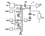
- FIG. 16 shows a circuit block configuration of a protection circuit 22 and an internal circuit 24 as an input-side protection circuit of the semiconductor device 2.
- the main electrode (first main electrode) of the MISFET 221 is connected between the external terminal 201 and the coupling capacitor 202 with the surge induction resistor 223 interposed. It is One end of the DC bias resistor 203 is connected between the coupling capacitor 202 and the internal circuit 24 , and the other end of the DC bias resistor 203 is connected to the decoupling capacitor 207 and the DC bias circuit 25 .
- the DC bias circuit 25 is built in the semiconductor device 2 instead of the external DC bias circuit 5 .
- the surge current Iesd flows through the surge induction resistor 223 and the pair of main electrodes of the MISFET 221 of the protection circuit 22 to the reference power supply GND side. flow.
- a constant punch-through voltage BVpth is applied between the pair of main electrodes of the MISFET 221 by adjusting the gate length dimension. Therefore, the surge voltage is reduced to the protection voltage Vesd, and the ESD protection function is obtained.
- the surge current Iesd flows from the reference power supply GND side to the external terminal 201 through the pair of main electrodes of the MISFET 221 and the surge induction resistor 223 .
- a resistor 222 is arranged between the gate electrode of the MISFET 221 and the main electrode used as the source electrode. Therefore, the gate potential of the gate electrode increases while the gate capacitance of the gate electrode is charged through the resistor 222 .
- a constant punch-through voltage BVpth is applied between the pair of main electrodes of the MISFET 221 by adjusting the gate length dimension, so the surge voltage is reduced to the protection voltage Vesd. In other words, since the gate potential does not rise above the protective voltage Vesd, it is possible to effectively suppress or prevent breakdown of the gate insulating film. Therefore, an ESD protection function is obtained.
- the protection circuit 22 and the semiconductor device 2 according to the third embodiment it is possible to obtain the same effects as those obtained by the protection circuit 22 and the semiconductor device 2 according to the first embodiment. Furthermore, in the protection circuit 22 and the semiconductor device 2, the single MISFET 221 can protect against positive and negative surges.
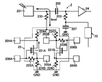
- a protection circuit 22 and a semiconductor device 2 according to a fourth embodiment of the present disclosure will be described.
- the fourth embodiment is a modification of the protection circuit 22 and the semiconductor device 2 according to the first embodiment.
- FIG. 17 shows a circuit block configuration of a protection circuit 22 and an internal circuit 24 as an input-side protection circuit of the semiconductor device 2. As shown in FIG. In the protection circuit 22 and the semiconductor device 2 according to the fourth embodiment, the protection circuit 22 is connected between the coupling capacitor 202 and the internal circuit 24 with the DC bias resistor 203 interposed.
- the protection circuit 22 includes two MISFETs 221A and 221B electrically connected in series that share a main electrode (here, a second main electrode) used as a drain electrode.
- the second main electrodes of the MISFET 221A and MISFET 221B are connected to the first external terminal 204.
- FIG. A main electrode (here, the first main electrode) used as the source electrode of the MISFET 221B is connected to the DC bias resistor 203 .
- a resistor 222A is electrically connected in series between the first main electrode and the gate electrode of the MISFET 221A.
- a first main electrode of the MISFET 221A is connected to the second external terminal 205A and the reference power supply GND.
- the gate electrode is connected to the third external terminal 206A.
- a resistor 222B is electrically connected in series between the first main electrode and gate electrode of the MISFET 221B.
- a first main electrode of the MISFET 221B is connected to the second external terminal 205B.
- the gate electrode is connected to the third external terminal 206B. That is, the MISFET 221A and the MISFET 221B are arranged symmetrically with the second main electrode as a boundary.
- An external DC bias circuit 5 is connected to the external power supply terminal 208 .
- hot carriers are injected into the charge storage section 219 in the order of the MISFET 221A and the MISFET 221B, or in the reverse order, or both at the same time.
- the second main electrodes of MISFET 221A and MISFET 221B are shared.
- a first main electrode of the MISFET 221B is connected to the external power supply terminal 208 .
- a first main electrode of the MISFET 221A is connected to the reference power supply GND.
- the protection voltage Vesd of the protection circuit 22 according to the fourth embodiment is approximately double that of the protection circuit 22 according to the first embodiment.
- the MISFET 221A and the MISFET 221B are arranged symmetrically, so the protection response characteristics are substantially the same.
- an external DC bias circuit 5 is connected to an external power supply terminal 208 of the semiconductor device 2 .
- a “positive” surge current Iesd flows from the DC bias circuit 5 through the external power supply terminal 208 to the semiconductor device 2 .
- the surge current Iesd flows through the MISFET 221B and MISFET 221A of the protection circuit 22 to the reference power supply GND.
- a resistor 222A is arranged between the gate electrode of the MISFET 221A and the first main electrode used as the source electrode.
- a resistor 222B is arranged between the gate electrode of the MISFET 221B and the main electrode used as the source electrode. Therefore, the surge current flowing from the source electrode side increases the gate potential of the gate electrode while charging the gate capacitance of the gate electrode through the resistor 222A or the resistor 222B.
- a constant punch-through voltage BVpth is obtained between the pair of main electrodes of the MISFET 221A and the MISFET 221B by adjusting the gate length dimension, so the surge voltage is reduced to the protection voltage Vesd.
- the gate potential does not rise above the protective voltage Vesd, it is possible to effectively suppress or prevent breakdown of the gate insulating film. Therefore, an ESD protection function is obtained.
- the protection circuit 22 and the semiconductor device 2 according to the fourth embodiment it is possible to obtain the same effects as those obtained by the protection circuit 22 and the semiconductor device 2 according to the first embodiment.
- the protection circuit 22 since the protection circuit 22 has the MISFET 221A and the MISFET 221B arranged symmetrically, it can cope with positive and negative surge voltages.
- the protection voltage Vesd is approximately double that of the protection circuit 22 according to the first embodiment, variations in the polarity of the punch-through voltage BVpth are suppressed, and the transient response characteristics are the same for positive and negative surge voltages.
- the protection voltage Vesd since the protection voltage Vesd is approximately double that of a single device, the withstand voltage of the RF signal is doubled, and the RF output can be increased.
- a protection circuit 22 and a semiconductor device 2 according to a fifth embodiment of the present disclosure will be described.
- the fifth embodiment is a modification obtained by combining the third embodiment and the fourth embodiment.
- FIG. 18 shows circuit block configurations of a protection circuit 22 and an internal circuit 24 as an input side protection circuit of the semiconductor device 2 .
- the protection circuit 22 is connected between the external terminal 201 and the coupling capacitor 202 with the surge induction resistor 223 interposed.
- the protection circuit 22 is composed of MISFETs 221A and 221B arranged symmetrically, like the protection circuit 22 according to the fourth embodiment.
- One end of the DC bias resistor 203 is connected between the coupling capacitor 202 and the internal circuit 24 , and the other end of the DC bias resistor 203 is connected to the decoupling capacitor 207 and the DC bias circuit 25 .
- the DC bias circuit 25 is built in the semiconductor device 2 instead of the external DC bias circuit 5 .
- the second main electrodes of MISFET 221A and MISFET 221B are shared.
- a first main electrode of MISFET 221B is connected to external terminal 201 through surge induction resistor 223 .
- a first main electrode of the MISFET 221A is connected to the reference power supply GND.
- the protection voltage Vesd of the protection circuit 22 according to the fifth embodiment is approximately double that of the protection circuit 22 according to the first embodiment.
- the MISFET 221A and the MISFET 221B are arranged symmetrically, so the protection response characteristics are substantially the same.
- the surge current Iesd flows through the surge induction resistance 223, the MISFETs 221B and 221A of the protection circuit 22 to the reference power supply GND side.
- a constant punch-through voltage BVpth is obtained between the pair of main electrodes of the MISFET 221A and the MISFET 221B by adjusting the gate length dimension. Therefore, the surge voltage is reduced to the protection voltage Vesd, and the ESD protection function is obtained.
- the surge current Iesd flows from the reference power supply GND side to the external terminal 201 through the MISFET 221A, MISFET 221B and surge induction resistor 223.
- a resistor 222A is arranged between the gate electrode of the MISFET 221A and the main electrode used as the source electrode.
- a resistor 222B is arranged between the gate electrode of the MISFET 221B and the main electrode used as the source electrode. Therefore, the surge current flowing from the source electrode side increases the gate potential of the gate electrode while charging the gate capacitance of the gate electrode through the resistor 222A or the resistor 222B.
- a constant punch-through voltage BVpth is obtained between the pair of main electrodes of the MISFET 221A and the MISFET 221B by adjusting the gate length dimension, so the surge voltage is reduced to the protection voltage Vesd.
- the gate potential does not rise above the protective voltage Vesd, it is possible to effectively suppress or prevent breakdown of the gate insulating film. Therefore, an ESD protection function is obtained.
- Sixth Embodiment> A protection circuit 22 and a semiconductor device 2 according to a sixth embodiment of the present disclosure will be described.
- the sixth embodiment is a modification of the protection circuit 22 and the semiconductor device 2 according to the fourth embodiment.
- FIG. 19 shows circuit block configurations of a protection circuit 22 and an internal circuit 24 as an input-side protection circuit of the semiconductor device 2 .
- the protection circuit 22 includes two electrically connected in series sharing a main electrode (here, the second main electrode) used as a source electrode. It has MISFETs 221A and MISFETs 221B. The second main electrodes of the MISFET 221A and MISFET 221B are connected to the second external terminal 205.
- FIG. A main electrode (here, a first main electrode) used as a drain electrode of the MISFET 221B is connected to the DC bias resistor 203 .
- a common resistor 222 is electrically connected in series between the second main electrode and the gate electrode of the MISFET 221A and between the MISFET 221B and the second main electrode.
- a first main electrode of the MISFET 221A is connected to the first external terminal 204A and the reference power supply GND.
- a gate electrode is connected to a third external terminal 206 common to the gate electrode of the MISFET 221B.
- the first main electrode of MISFET 221B is connected to first external terminal 204B.
- the MISFET 221A and the MISFET 221B are arranged symmetrically with the second main electrode as a boundary.
- An external DC bias circuit 5 is connected to the external power supply terminal 208 .
- the second main electrodes of MISFET 221A and MISFET 221B are shared.
- a first main electrode of the MISFET 221B is connected to the external power supply terminal 208 .
- a first main electrode of the MISFET 221A is connected to the reference power supply GND. Therefore, the protection voltage Vesd of the protection circuit 22 according to the sixth embodiment is approximately double that of the protection circuit 22 according to the first embodiment. Also, in the protection circuit 22 according to the first embodiment, there is a slight difference in the response characteristics to the protection of the "positive" surge and the "negative" surge. On the other hand, in the protection circuit 22 according to the sixth embodiment, the MISFET 221A and the MISFET 221B are arranged symmetrically, so the protection response characteristics are substantially the same.
- an external DC bias circuit 5 is connected to an external power supply terminal 208 of the semiconductor device 2 .
- a “positive” surge current Iesd flows from the DC bias circuit 5 through the external power supply terminal 208 to the semiconductor device 2 .
- the surge current Iesd flows through the MISFET 221B and MISFET 221A of the protection circuit 22 to the reference power supply GND.
- a resistor 222 is arranged between the gate electrode of the MISFET 221A and the MISFET 221B and the second main electrode used as the source electrode. Therefore, the surge current flowing from the source electrode side increases the gate potential of the gate electrode while charging the gate capacitance of the gate electrode through the resistor 222 .
- a constant punch-through voltage BVpth is obtained between the pair of main electrodes of the MISFET 221A and the MISFET 221B by adjusting the gate length dimension, so the surge voltage is reduced to the protection voltage Vesd.
- the gate potential does not rise above the protective voltage Vesd, it is possible to effectively suppress or prevent breakdown of the gate insulating film. Therefore, an ESD protection function is obtained.
- Seventh Embodiment> A protection circuit 22 and a semiconductor device 2 according to a seventh embodiment of the present disclosure will be described.
- the seventh embodiment is an example in which the protection circuit 22 and the semiconductor device 2 according to the fifth embodiment and the protection circuit 22 and the semiconductor device 2 according to the sixth embodiment are combined.
- FIG. 20 shows circuit block configurations of a protection circuit 22 and an internal circuit 24 as an input-side protection circuit of the semiconductor device 2 .
- the protection circuit 22 is connected between the external terminal 201 and the coupling capacitor 202 with the surge induction resistor 223 interposed.
- the protection circuit 22 is composed of MISFETs 221A and 221B arranged symmetrically, like the protection circuit 22 according to the sixth embodiment.
- One end of the DC bias resistor 203 is connected between the coupling capacitor 202 and the internal circuit 24 , and the other end of the DC bias resistor 203 is connected to the decoupling capacitor 207 and the DC bias circuit 25 .
- the DC bias circuit 25 is built in the semiconductor device 2 instead of the external DC bias circuit 5 .
- the second main electrodes of MISFET 221A and MISFET 221B are shared.
- a first main electrode of MISFET 221B is connected to external terminal 201 through surge induction resistor 223 .
- a first main electrode of the MISFET 221A is connected to the reference power supply GND. Therefore, the protection voltage Vesd of the protection circuit 22 according to the seventh embodiment is approximately double that of the protection circuit 22 according to the first embodiment. Also, in the protection circuit 22 according to the first embodiment, there is a slight difference in the response characteristics for protection of "positive" surges and "negative" surges. On the other hand, in the protection circuit 22 according to the seventh embodiment, the MISFET 221A and the MISFET 221B are arranged symmetrically, so the protection response characteristics are substantially the same.
- the surge current Iesd flows through the surge induction resistance 223, the MISFETs 221B and 221A of the protection circuit 22 to the reference power supply GND side.
- a constant punch-through voltage BVpth is obtained between the pair of main electrodes of the MISFET 221A and the MISFET 221B by adjusting the gate length dimension. Therefore, the surge voltage is reduced to the protection voltage Vesd, and the ESD protection function is obtained.
- the surge current Iesd flows from the reference power supply GND side to the external terminal 201 through the MISFET 221A, MISFET 221B and surge induction resistor 223.
- a resistor 222 is arranged between the gate electrode of the MISFET 221A and the MISFET 221B and the main electrode used as the source electrode. Therefore, the surge current flowing from the source electrode side increases the gate potential of the gate electrode while charging the gate capacitance of the gate electrode through the resistor 222 . At this time, a constant punch-through voltage BVpth is obtained between the pair of main electrodes of the MISFET 221A and the MISFET 221B by adjusting the gate length dimension, so the surge voltage is reduced to the protection voltage Vesd. In other words, since the gate potential does not rise above the protective voltage Vesd, it is possible to effectively suppress or prevent breakdown of the gate insulating film. Therefore, an ESD protection function is obtained.
- Eighth Embodiment> A protection circuit 22 and a semiconductor device 2 according to an eighth embodiment of the present disclosure will be described.
- the eighth embodiment is a modification of the protection circuit 22 and the semiconductor device 2 according to the sixth embodiment.
- FIG. 21 shows circuit block configurations of a protection circuit 22 and an internal circuit 24 as an input-side protection circuit of the semiconductor device 2 .
- the protection circuit 22 is connected between the coupling capacitor 202 and the internal circuit 24 with the DC bias resistor 203 interposed.
- the protection circuit 22 includes two MISFETs 221A and 221B electrically connected in parallel.
- the first main electrode used as the drain region of the MISFET 221A is connected to the first external terminal 204A and also to the DC bias resistor 203 via the current relaxation resistor 224A.
- the second main electrode used as the source electrode is connected to the second external terminal 205A and to the reference power supply GND via the current relaxation resistor 224B.
- the gate electrode is connected to the third external terminal 206A.
- a resistor 222A is electrically connected in series between the second main electrode and the gate electrode.
- Each of the current relaxation resistors 224A and 224B relaxes current flow during injection of hot carriers.
- a first main electrode used as a drain region of the MISFET 221B is connected to the first external terminal 204B and also connected to the reference power supply GND via a current relaxation resistor 224C.
- a second main electrode used as a source electrode is connected to the second external terminal 205B and to the DC bias resistor 203 via a current relaxation resistor 224D.
- the gate electrode is connected to the third external terminal 206B.
- a resistor 222B is electrically connected in series between the second main electrode and the gate electrode.
- Each of the current relaxation resistors 224C and 224D relaxes current flow during injection of hot carriers.
- the MISFET 221A and the MISFET 221B are configured such that the polarities of the first main electrode and the second main electrode are opposite to each other.
- An external DC bias circuit 5 is connected to the external power supply terminal 208 .
- the protection voltage Vesd of the protection circuit 22 is equivalent to the protection voltage Vesd of the protection circuit 22 according to the first embodiment.
- the protection circuit 22 according to the first embodiment there is a slight difference in the response characteristics for protection of "positive" surges and "negative” surges.
- the polarities of the MISFET 221A and the MISFET 221B are opposite to each other, so the protection response characteristics are substantially the same.
- an external DC bias circuit 5 is connected to an external power supply terminal 208 of the semiconductor device 2 .
- a “positive” surge current Iesd flows from the DC bias circuit 5 through the external power supply terminal 208 to the semiconductor device 2 .
- the surge current Iesd flows through the MISFET 221A of the protection circuit 22 to the reference power supply GND.
- a resistor 222A is arranged between the gate electrode of the MISFET 221A and the second main electrode.
- a resistor 222B is arranged between the gate electrode of the MISFET 221B and the second main electrode. Therefore, the surge current flowing from the source electrode side increases the gate potential of the gate electrode while charging the gate capacitance of the gate electrode through the resistor 222A or the resistor 222B.
- a constant punch-through voltage BVpth is obtained between the pair of main electrodes of the MISFET 221A and the MISFET 221B by adjusting the gate length dimension, so the surge voltage is reduced to the protection voltage Vesd.
- the gate potential does not rise above the protective voltage Vesd, it is possible to effectively suppress or prevent breakdown of the gate insulating film. Therefore, an ESD protection function is obtained.
- the protection circuit 22 and the semiconductor device 2 according to the eighth embodiment it is possible to obtain the same effects as those obtained by the protection circuit 22 and the semiconductor device 2 according to the first embodiment. Furthermore, since the protection circuit 22 includes the MISFET 221A and the MISFET 221B arranged with opposite polarities, it is possible to effectively suppress variations in surge polarities. Also, the transient response characteristics can be made equal to positive and negative surges.
- a protection circuit 22 and a semiconductor device 2 according to a ninth embodiment of the present disclosure will be described.
- the ninth embodiment is an example in which the protection circuit 22 and the semiconductor device 2 according to the seventh embodiment and the protection circuit 22 and the semiconductor device 2 according to the eighth embodiment are combined.
- FIG. 22 shows a circuit block configuration of a protection circuit 22 and an internal circuit 24 as an input-side protection circuit of the semiconductor device 2. As shown in FIG. In the protection circuit 22 and the semiconductor device 2 according to the ninth embodiment, the protection circuit 22 is connected between the external terminal 201 and the coupling capacitor 202 with the surge induction resistor 223 interposed.
- the protection circuit 22 includes two MISFETs 221A and 221B electrically connected in parallel, like the protection circuit 22 according to the eighth embodiment.
- the configuration and circuit operation other than the above are substantially the same as the configuration and circuit operation of the protection circuit 22 according to the seventh embodiment and the protection circuit 22 according to the eighth embodiment, so descriptions thereof are omitted here. do.
- Tenth Embodiment> A protection circuit 22 and a semiconductor device 2 according to the tenth embodiment of the present disclosure will be described.
- the tenth embodiment is a modification of the protection circuit 22 and the semiconductor device 2 according to the eighth embodiment.
- FIG. 23 shows a circuit block configuration of a protection circuit 22 and an internal circuit 24 as an input-side protection circuit of the semiconductor device 2. As shown in FIG. In the protection circuit 22 and the semiconductor device 2 according to the tenth embodiment, the protection circuit 22 is connected between the coupling capacitor 202 and the internal circuit 24 with the DC bias resistor 203 interposed.
- the protection circuit 22 includes two MISFETs 221A and 221B electrically connected in parallel.
- a first main electrode used as a drain region of the MISFET 221A is connected to the first external terminal 204A and to the DC bias resistor 203.
- a second main electrode used as a source electrode is connected to the first external terminal 204B and to the reference power supply GND.
- the gate electrode is connected to the third external terminal 206A.
- a resistor 222A is electrically connected in series between the second main electrode and the gate electrode.
- a first main electrode used as a drain region of the MISFET 221B is connected to the first external terminal 204B and to the reference power supply GND.
- the first external terminal 204B is also connected to the second main electrode of the MISFET 221A.
- a second main electrode used as a source electrode is connected to the first external terminal 204A and to the DC bias resistor 203 .
- the first external terminal 204A is also connected to the first main electrode of the MISFET 221A.
- the gate electrode is connected to the third external terminal 206B.
- a resistor 222B is electrically connected in series between the second main electrode and the gate electrode.
- the MISFET 221A and the MISFET 221B are configured such that the polarities of the first main electrode and the second main electrode are opposite to each other.
- An external DC bias circuit 5 is connected to the external power supply terminal 208 .
- the protection voltage Vesd of the protection circuit 22 is equivalent to the protection voltage Vesd of the protection circuit 22 according to the first embodiment.
- the protection circuit 22 according to the first embodiment there is a slight difference in the response characteristics for protection of "positive" surges and "negative” surges.
- the protection circuit 22 according to the tenth embodiment since the polarities of the MISFET 221A and the MISFET 221B are opposite to each other, the response characteristics to protection are substantially the same.
- an external DC bias circuit 5 is connected to an external power supply terminal 208 of the semiconductor device 2 .
- a “positive” surge current Iesd flows from the DC bias circuit 5 through the external power supply terminal 208 to the semiconductor device 2 .
- the surge current Iesd flows through the MISFET 221A of the protection circuit 22 to the reference power supply GND.
- a resistor 222A is arranged between the gate electrode of the MISFET 221A and the second main electrode.
- a resistor 222B is arranged between the gate electrode of the MISFET 221B and the second main electrode. Therefore, the surge current flowing from the source electrode side increases the gate potential of the gate electrode while charging the gate capacitance of the gate electrode through the resistor 222A or the resistor 222B.
- a constant punch-through voltage BVpth is obtained between the pair of main electrodes of the MISFET 221A and the MISFET 221B by adjusting the gate length dimension, so the surge voltage is reduced to the protection voltage Vesd.
- the gate potential does not rise above the protective voltage Vesd, it is possible to effectively suppress or prevent breakdown of the gate insulating film. Therefore, an ESD protection function is obtained.
- the protection circuit 22 and the semiconductor device 2 according to the tenth embodiment it is possible to obtain the same effects as those obtained by the protection circuit 22 and the semiconductor device 2 according to the eighth embodiment.
- the first external terminal 204A is also used as an external terminal that connects the first main electrode of the MISFET 221A and the second main electrode of the MISFET 221B.
- the second external terminal 204B is also used as an external terminal connecting the second main electrode of the MISFET 221A and the first main electrode of the MISFET 221B. Therefore, the number of external terminals into which hot carriers are injected can be reduced.
- a protection circuit 22 and a semiconductor device 2 according to the eleventh embodiment of the present disclosure will be described.
- the eleventh embodiment is an example in which the protection circuit 22 and the semiconductor device 2 according to the ninth embodiment and the protection circuit 22 and the semiconductor device 2 according to the tenth embodiment are combined.
- FIG. 24 shows circuit block configurations of a protection circuit 22 and an internal circuit 24 as an input side protection circuit of the semiconductor device 2 .
- the protection circuit 22 is connected between the external terminal 201 and the coupling capacitor 202 with the surge induction resistor 223 interposed therebetween.
- the protection circuit 22 includes two MISFETs 221A and 221B electrically connected in parallel, like the protection circuit 22 according to the tenth embodiment.
- the configuration and circuit operation other than the above are substantially the same as the configuration and circuit operation of the protection circuit 22 according to the ninth embodiment and the protection circuit 22 according to the tenth embodiment, so descriptions thereof are omitted here. do.
- a protection circuit 22 and a semiconductor device 2 according to a twelfth embodiment of the present disclosure will be described.
- the twelfth embodiment is a modification of the protection circuit 22 and the semiconductor device 2 according to the first embodiment.
- FIG. 25 shows circuit block configurations of a protection circuit 22 and an internal circuit 24 as an input-side protection circuit of the semiconductor device 2 .
- the external protection element 6 is electrically connected in parallel with the DC bias circuit 5 to the external power supply terminal 208 .
- the external protection element 6 has an ESD protection tolerance higher than that of the protection circuit 22 .
- a GGnMOS-Tr Gate Grounded n-type MOSFET
- a pn diode or the like can be practically used for the external protection element 6 .
- the present technology is not limited to the above-described embodiments, and can be modified in various ways without departing from the scope of the present technology.
- the protection circuits and semiconductor devices according to the first to twelfth embodiments may be combined.
- the present technology has been described using the input-side protection circuit as an example, it may be applied to an output-side protection circuit.
- the present technology is not limited to insulated gate field effect transistors formed of compound semiconductor materials, and may be applied to protection circuits and semiconductor devices including insulated gate field effect transistors formed of Si semiconductor materials.
- a protection circuit includes a MISFET.
- a MISFET has a first main electrode connected between an external terminal and an internal circuit, and a second main electrode connected to a reference power supply.
- a charge accumulating portion capable of accumulating hot carriers is provided in the gate insulating film.
- the MISFET is formed as a depletion type, and can be formed to have an enhancement-type threshold voltage by accumulating hot carriers in the charge storage section. Therefore, it is possible to construct a protection circuit excellent in ESD tolerance or avalanche tolerance without using a pn junction and using a MISFET with high process affinity.
- the semiconductor device includes an external terminal, an internal circuit, and a protection circuit.
- the protection circuit is arranged on the semiconductor substrate and has a MISFET.
- a MISFET has a first main electrode connected between an external terminal and an internal circuit, a second main electrode and a gate electrode connected to a reference power supply, and a charge storage section capable of storing hot carriers. Therefore, it is possible to obtain the same effects as those obtained by the protection circuit described above.
- the present technology has the following configuration. According to the present technology having the following configuration, it is possible to construct a protection circuit and a semiconductor device excellent in ESD tolerance or avalanche tolerance using MISFETs with high process affinity.
- a first main electrode is connected between an external terminal and an internal circuit, a second main electrode and a gate electrode are connected to a reference power source, and a charge storage portion capable of storing hot carriers is provided on the gate insulating film.
- a protection circuit comprising: a disposed first insulated gate field effect transistor.
- the protection circuit according to (1) further comprising a resistor electrically connected in series between the gate electrode and the second main electrode.
- a semiconductor device comprising (5) The semiconductor device according to (4), wherein the protection circuit further includes a resistor electrically connected in series between the gate electrode and the second main electrode. (6) a first external terminal connected between the external terminal and the first main electrode and supplied with a first power source for generating hot carriers; a second external terminal connected to the second main electrode and supplied with a second power supply for generating hot carriers; The semiconductor device according to (4) or (5), further comprising a third external terminal connected to the gate electrode and supplied with a third power supply that generates hot carriers.
- the charge storage section has a structure in which an oxide film, a nitride film, and an oxide film are sequentially laminated.
- the nitride film contains SiN;
- the oxide film contains at least one selected from Al 2 O 3 , HfO 2 , Ta 2 O 5 , ZrO 2 , Y 2 O 3 and SiO 2 .
- the charge storage section includes Al 2 O 3 , HfO 2 laminated on the Al 2 O 3 , SiN laminated on the HfO 2 , and SiO 2 laminated on the SiN.
- the compound semiconductor contains GaN or GaAs.
- the first insulated gate field effect transistor contains InAlN.
- the first insulated gate field effect transistor accumulates hot carriers in the charge storage section and shifts the threshold voltage from the depletion type to the positive direction to form the enhancement type from (4) to (12). ).
- the gate length of the first insulated gate field effect transistor in the direction coinciding with the direction in which the first main electrode and the second main electrode are arranged is 0.05 ⁇ m or more and 0.3 ⁇ m or less;
- the resistor has a resistance of 100 ⁇ to 10M ⁇ .
- each of the first insulated gate field effect transistor and the second insulated gate field effect transistor contains InAlN;
Abstract
This protection circuit comprises a first insulated gate field-effect transistor, a first main electrode of which is connected between an external terminal and an internal circuit, a second main electrode and a gate electrode of which are connected to a standard power source, and in which a charge accumulation unit capable of accumulating hot carriers is provided to a gate insulating film.
Description
本開示は、保護回路及び半導体装置に関する。
The present disclosure relates to protection circuits and semiconductor devices.
特許文献1には、静電気保護素子付き高周波集積回路が開示されている。静電気保護素子は、ディプレッション型電界効果トランジスタとエンハンスメント型電界効果トランジスタとを電気的に直列に接続し、更にエンハンスメント型電界効果トランジスタに電気的に並列にキャパシタを接続している。電界効果トランジスタは、MESFET、ゲート接合型FET、HEMT等により構成されている。
外部からノイズ又は高電圧パルスが入力されたとき、静電気保護素子では、エンハンスメント型電界効果トランジスタがブレークダウン動作し、そのインピーダンスが低くされて、ノイズ又は高電圧パルスを放電することができる。Patent Document 1 discloses a high-frequency integrated circuit with an electrostatic protection element. The static electricity protection element has a depletion field effect transistor and an enhancement field effect transistor electrically connected in series, and further has a capacitor electrically connected in parallel with the enhancement field effect transistor. A field effect transistor is composed of a MESFET, a gate junction type FET, a HEMT, or the like.
When noise or a high voltage pulse is input from the outside, in the electrostatic protection device, the enhancement field effect transistor breaks down, the impedance is lowered, and the noise or the high voltage pulse can be discharged.
外部からノイズ又は高電圧パルスが入力されたとき、静電気保護素子では、エンハンスメント型電界効果トランジスタがブレークダウン動作し、そのインピーダンスが低くされて、ノイズ又は高電圧パルスを放電することができる。
When noise or a high voltage pulse is input from the outside, in the electrostatic protection device, the enhancement field effect transistor breaks down, the impedance is lowered, and the noise or the high voltage pulse can be discharged.
また、特許文献2には、サージ保護素子及び半導体装置が開示されている。サージ保護素子は、pnpバイポーラトランジスタにより構成されている。このバイポーラトランジスタは、p型GaN層をコレクタ領域、AlGaN層及びGaN層をベース領域、p型GaN層をエミッタ領域として構成されている。
サージ保護素子では、サージがパンチスルー電流として吸収される。 Further,Patent Document 2 discloses a surge protection element and a semiconductor device. The surge protection element is composed of a pnp bipolar transistor. This bipolar transistor has a p-type GaN layer as a collector region, an AlGaN layer and a GaN layer as a base region, and a p-type GaN layer as an emitter region.
A surge protection device absorbs a surge as a punch-through current.
サージ保護素子では、サージがパンチスルー電流として吸収される。 Further,
A surge protection device absorbs a surge as a punch-through current.
さらに、特許文献3には、静電破壊保護回路を備えた半導体集積回路が開示されている。静電破壊保護回路は、ダイオード接続されたトランジスタにより構成されている。トランジスタには、バイポーラトランジスタ又はMOSFETが使用されている。
Furthermore, Patent Document 3 discloses a semiconductor integrated circuit equipped with an electrostatic discharge protection circuit. The electrostatic breakdown protection circuit is composed of a diode-connected transistor. Bipolar transistors or MOSFETs are used for the transistors.
次世代携帯端末向けとして、ミリ波帯において動作する高周波パワーアンプが開発されている。高周波パワーアンプの構築には、GaN系ワイドバンドギャップ材料を用いた絶縁ゲート電界効果トランジスタが使用されている。具体的には、金属体-絶縁体-半導体型電界効果トランジスタ(Metal Insulator Semiconductor Field Effect Transistor。以下、単に「MISFET」という。)が使用されている。
上記特許文献1に開示されている静電気保護素子、特許文献2に開示されているサージ保護素子、特許文献3に開示されている静電破壊保護回路のそれぞれでは、p型層が使用されている。GaN系プロセスにおいて、p型不純物の活性化率は非常に低いので、p型GaNを製作することが難く、製造工程におけるプロセス親和性(量産性)が乏しい。つまり、p型GaNを用いた保護素子の実現が難しい。このため、静電気放電(Electro Static Discharge。以下、単に「ESD」という。)耐量又はアバランシェ(Avalanche)耐量に優れた保護回路及び半導体装置が望まれている。 High-frequency power amplifiers operating in the millimeter wave band have been developed for next-generation mobile terminals. Insulated gate field effect transistors using GaN-based wide bandgap materials are used to construct high frequency power amplifiers. Specifically, a metal-insulator-semiconductor field-effect transistor (hereinafter referred to simply as "MISFET") is used.
A p-type layer is used in each of the electrostatic protection element disclosed inPatent Document 1, the surge protection element disclosed in Patent Document 2, and the electrostatic discharge protection circuit disclosed in Patent Document 3. . In the GaN-based process, the activation rate of p-type impurities is very low, so it is difficult to manufacture p-type GaN, and the process affinity (mass productivity) in the manufacturing process is poor. In other words, it is difficult to realize a protective element using p-type GaN. Therefore, there is a demand for a protection circuit and a semiconductor device that are excellent in Electro Static Discharge (hereinafter simply referred to as "ESD") or avalanche resistance.
上記特許文献1に開示されている静電気保護素子、特許文献2に開示されているサージ保護素子、特許文献3に開示されている静電破壊保護回路のそれぞれでは、p型層が使用されている。GaN系プロセスにおいて、p型不純物の活性化率は非常に低いので、p型GaNを製作することが難く、製造工程におけるプロセス親和性(量産性)が乏しい。つまり、p型GaNを用いた保護素子の実現が難しい。このため、静電気放電(Electro Static Discharge。以下、単に「ESD」という。)耐量又はアバランシェ(Avalanche)耐量に優れた保護回路及び半導体装置が望まれている。 High-frequency power amplifiers operating in the millimeter wave band have been developed for next-generation mobile terminals. Insulated gate field effect transistors using GaN-based wide bandgap materials are used to construct high frequency power amplifiers. Specifically, a metal-insulator-semiconductor field-effect transistor (hereinafter referred to simply as "MISFET") is used.
A p-type layer is used in each of the electrostatic protection element disclosed in
本技術は、ESD耐量又はアバランシェ耐量に優れた保護回路及び半導体装置を提供する。
This technology provides a protection circuit and a semiconductor device with excellent ESD resistance or avalanche resistance.
本開示の第1実施態様に係る保護回路は、外部端子と内部回路との間に第1主電極が接続され、基準電源に第2主電極及びゲート電極が接続されるとともに、ホットキャリアを蓄積可能な電荷蓄積部がゲート絶縁膜に配設された第1絶縁ゲート電界効果トランジスタを備えている。
A protection circuit according to a first embodiment of the present disclosure has a first main electrode connected between an external terminal and an internal circuit, a second main electrode and a gate electrode connected to a reference power supply, and accumulates hot carriers. It comprises a first insulated gate field effect transistor with a possible charge storage disposed in the gate insulator.
本開示の第2実施態様に係る半導体装置は、基板に配設された外部端子と、基板に配設され、外部端子に接続された内部回路と、基板に配設され、外部端子と内部回路との間に第1主電極が接続され、基準電源に第2主電極及びゲート電極が接続されるとともに、ホットキャリアが蓄積可能な電荷蓄積部がゲート絶縁膜に配設された第1絶縁ゲート電界効果トランジスタを有する保護回路と、を備えている。
A semiconductor device according to a second embodiment of the present disclosure comprises: an external terminal provided on a substrate; an internal circuit provided on the substrate and connected to the external terminal; A first insulating gate having a first main electrode connected between and, a second main electrode and a gate electrode connected to a reference power supply, and a charge accumulating portion capable of accumulating hot carriers disposed in a gate insulating film. a protection circuit comprising a field effect transistor.
以下、本開示の実施の形態について図面を参照して詳細に説明する。なお、説明は以下の順序で行う。
1.第1実施の形態
第1実施の形態は、保護回路及び内部回路を搭載した半導体装置を実装する高周波(Radio Frequency。以下、単に「RF」という。)パワーアンプモジュールに、本技術を適用した第1例を説明する。ここでは、RFパワーアンプモジュールの構成、半導体装置のレイアウト、保護回路及び内部回路の回路ブロックの構成、縦断面構造、平面構造、製造方法及び保護回路の閾値電圧の調整方法について説明する。
2.第2実施の形態
第2実施の形態は、第1実施の形態に係る半導体装置において、保護回路の構成を変えた第2例を説明する。
3.第3実施の形態
第3実施の形態は、第1実施の形態に係る半導体装置において、保護回路の構成を変えた第3例を説明する。
4.第4実施の形態
第4実施の形態は、第1実施の形態に係る半導体装置において、保護回路の構成を変えた第4例を説明する。
5.第5実施の形態
第5実施の形態は、第3実施の形態に係る半導体装置と第4実施の形態に係る半導体装置とを組み合わせた第5例を説明する。
6.第6実施の形態
第6実施の形態は、第4実施の形態に係る半導体装置において、保護回路の構成を変えた第6例を説明する。
7.第7実施の形態
第7実施の形態は、第5実施の形態に係る半導体装置と第6実施の形態に係る半導体装置とを組み合わせた第7例を説明する。
8.第8実施の形態
第8実施の形態は、第6実施の形態に係る半導体装置において、保護回路の構成を変えた第8例を説明する。
9.第9実施の形態
第9実施の形態は、第7実施の形態に係る半導体装置と第8実施の形態に係る半導体装置とを組み合わせた第9例を説明する。
10.第10実施の形態
第10実施の形態は、第8実施の形態に係る半導体装置において、保護回路の構成を変えた第10例を説明する。
11.第11実施の形態
第11実施の形態は、第9実施の形態に係る半導体装置と第10実施の形態に係る半導体装置とを組み合わせた第11例を説明する。
12.第12実施の形態
第12実施の形態は、第1実施の形態に係る半導体装置において、保護回路の構成を変えた第12例を説明する。
13.その他の実施の形態 Hereinafter, embodiments of the present disclosure will be described in detail with reference to the drawings. The description will be made in the following order.
1. First Embodiment The first embodiment is a radio frequency (hereinafter simply referred to as "RF") power amplifier module mounted with a semiconductor device equipped with a protection circuit and an internal circuit. One example is explained. Here, the configuration of the RF power amplifier module, the layout of the semiconductor device, the configuration of the circuit blocks of the protection circuit and the internal circuit, the vertical cross-sectional structure, the planar structure, the manufacturing method, and the adjustment method of the threshold voltage of the protection circuit will be described.
2. Second Embodiment A second embodiment will explain a second example in which the configuration of the protection circuit is changed in the semiconductor device according to the first embodiment.
3. Third Embodiment A third embodiment will explain a third example in which the configuration of the protection circuit is changed in the semiconductor device according to the first embodiment.
4. Fourth Embodiment A fourth embodiment will explain a fourth example in which the configuration of the protection circuit in the semiconductor device according to the first embodiment is changed.
5. Fifth Embodiment A fifth embodiment will explain a fifth example in which the semiconductor device according to the third embodiment and the semiconductor device according to the fourth embodiment are combined.
6. Sixth Embodiment A sixth embodiment will explain a sixth example in which the configuration of the protection circuit is changed in the semiconductor device according to the fourth embodiment.
7. Seventh Embodiment A seventh embodiment describes a seventh example in which the semiconductor device according to the fifth embodiment and the semiconductor device according to the sixth embodiment are combined.
8. Eighth Embodiment The eighth embodiment describes an eighth example in which the configuration of the protection circuit is changed in the semiconductor device according to the sixth embodiment.
9. Ninth Embodiment A ninth embodiment describes a ninth example in which the semiconductor device according to the seventh embodiment and the semiconductor device according to the eighth embodiment are combined.
10. Tenth Embodiment A tenth embodiment will explain a tenth example in which the configuration of the protection circuit is changed in the semiconductor device according to the eighth embodiment.
11. Eleventh Embodiment The eleventh embodiment describes an eleventh example in which the semiconductor device according to the ninth embodiment and the semiconductor device according to the tenth embodiment are combined.
12. Twelfth Embodiment A twelfth embodiment will explain a twelfth example in which the configuration of the protection circuit in the semiconductor device according to the first embodiment is changed.
13. Other embodiments
<1.第1実施の形態>
図1~図14を用いて、本開示の第1実施の形態に係る保護回路22、保護回路23及び半導体装置2を説明する。
ここで、図中、適宜、示される矢印X方向は、便宜的に平面上に載置された半導体装置2の1つの平面方向を示している。矢印Y方向は、矢印X方向に対して直交する他の1つの平面方向を示している。また、矢印Z方向は、矢印X方向及び矢印Y方向に対して直交する上方向を示している。つまり、矢印X方向、矢印Y方向、矢印Z方向は、丁度、三次元座標系のX軸方向、Y軸方向、Z軸方向に各々一致している。
なお、これらの各方向は、説明の理解を助けるために示されており、本技術の方向を限定するものではない。 <1. First Embodiment>
Aprotection circuit 22, a protection circuit 23, and a semiconductor device 2 according to the first embodiment of the present disclosure will be described with reference to FIGS. 1 to 14. FIG.
Here, in the drawing, the arrow X direction shown as appropriate indicates one plane direction of thesemiconductor device 2 placed on the plane for the sake of convenience. The arrow Y direction indicates another planar direction perpendicular to the arrow X direction. Also, the arrow Z direction indicates an upward direction orthogonal to the arrow X direction and the arrow Y direction. That is, the arrow X direction, the arrow Y direction, and the arrow Z direction exactly match the X-axis direction, the Y-axis direction, and the Z-axis direction of the three-dimensional coordinate system, respectively.
It should be noted that each of these directions is shown to aid understanding of the description and is not intended to limit the direction of the present technology.
図1~図14を用いて、本開示の第1実施の形態に係る保護回路22、保護回路23及び半導体装置2を説明する。
ここで、図中、適宜、示される矢印X方向は、便宜的に平面上に載置された半導体装置2の1つの平面方向を示している。矢印Y方向は、矢印X方向に対して直交する他の1つの平面方向を示している。また、矢印Z方向は、矢印X方向及び矢印Y方向に対して直交する上方向を示している。つまり、矢印X方向、矢印Y方向、矢印Z方向は、丁度、三次元座標系のX軸方向、Y軸方向、Z軸方向に各々一致している。
なお、これらの各方向は、説明の理解を助けるために示されており、本技術の方向を限定するものではない。 <1. First Embodiment>
A
Here, in the drawing, the arrow X direction shown as appropriate indicates one plane direction of the
It should be noted that each of these directions is shown to aid understanding of the description and is not intended to limit the direction of the present technology.
[保護回路22及び半導体装置2の構成]
(1)RFパワーアンプモジュール1の平面レイアウト構成
図1は、RFパワーアンプモジュール1の平面レイアウトを表している。
RFパワーアンプモジュール1は、入力部整合回路3と、半導体装置2と、出力部整合回路4と、直流(Direct Current。以下、単に「DC」という。)バイアス回路5と、を備えている。これら入力部整合回路3等は基板10上に実装されている。実装には、例えば半田が使用されている。 [Configuration ofprotection circuit 22 and semiconductor device 2]
(1) Planar Layout Configuration of RFPower Amplifier Module 1 FIG. 1 shows a plan layout of the RF power amplifier module 1 .
The RFpower amplifier module 1 includes an input matching circuit 3 , a semiconductor device 2 , an output matching circuit 4 , and a direct current (hereinafter simply referred to as “DC”) bias circuit 5 . These input matching circuits 3 and the like are mounted on the substrate 10 . Solder, for example, is used for mounting.
(1)RFパワーアンプモジュール1の平面レイアウト構成
図1は、RFパワーアンプモジュール1の平面レイアウトを表している。
RFパワーアンプモジュール1は、入力部整合回路3と、半導体装置2と、出力部整合回路4と、直流(Direct Current。以下、単に「DC」という。)バイアス回路5と、を備えている。これら入力部整合回路3等は基板10上に実装されている。実装には、例えば半田が使用されている。 [Configuration of
(1) Planar Layout Configuration of RF
The RF
基板10はモジュール基板として形成されている。基板10は、矢印Z方向から見て(以下、単に「平面視において」という。)、例えば矩形状に形成されている。
入力部整合回路3は、ここでは基板10の左側上方に実装されている。入力部整合回路3には、RFパワーアンプモジュール1の外部からRF信号が入力される。 Thesubstrate 10 is formed as a module substrate. The substrate 10 is formed in, for example, a rectangular shape when viewed from the direction of the arrow Z (hereinafter simply referred to as "plan view").
Theinput matching circuit 3 is mounted on the upper left side of the substrate 10 here. An RF signal is input to the input unit matching circuit 3 from the outside of the RF power amplifier module 1 .
入力部整合回路3は、ここでは基板10の左側上方に実装されている。入力部整合回路3には、RFパワーアンプモジュール1の外部からRF信号が入力される。 The
The
半導体装置2は、基板10の中央に実装されている。半導体装置2は、保護回路22と、内部回路24と、保護回路23とを備えている。
保護回路22は入力側保護回路として構成されている。保護回路22は、入力部整合回路3、内部回路24のそれぞれに接続されている。
内部回路24は、第1実施の形態において、RFパワーアンプを備えている。例えば、内部回路24は、第5世代又はそれ以降の世代の携帯端末向けとして、ミリ波帯において動作するRFパワーアンプを備えている。
保護回路23は出力側保護回路として構成されている。保護回路23は、内部回路24、出力部整合回路4のそれぞれに接続されている。なお、保護回路23の構成は、保護回路22の構成と同様であるので、以降の説明を省略する。 Thesemiconductor device 2 is mounted in the center of the substrate 10 . The semiconductor device 2 includes a protection circuit 22 , an internal circuit 24 and a protection circuit 23 .
Theprotection circuit 22 is configured as an input side protection circuit. The protection circuit 22 is connected to each of the input matching circuit 3 and the internal circuit 24 .
Theinternal circuit 24 has an RF power amplifier in the first embodiment. For example, the internal circuitry 24 includes an RF power amplifier operating in the millimeter wave band for fifth generation or later generation mobile terminals.
Theprotection circuit 23 is configured as an output side protection circuit. The protection circuit 23 is connected to each of the internal circuit 24 and the output matching circuit 4 . Since the configuration of the protection circuit 23 is the same as that of the protection circuit 22, the description thereof will be omitted.
保護回路22は入力側保護回路として構成されている。保護回路22は、入力部整合回路3、内部回路24のそれぞれに接続されている。
内部回路24は、第1実施の形態において、RFパワーアンプを備えている。例えば、内部回路24は、第5世代又はそれ以降の世代の携帯端末向けとして、ミリ波帯において動作するRFパワーアンプを備えている。
保護回路23は出力側保護回路として構成されている。保護回路23は、内部回路24、出力部整合回路4のそれぞれに接続されている。なお、保護回路23の構成は、保護回路22の構成と同様であるので、以降の説明を省略する。 The
The
The
The
出力部整合回路4は、基板10の右側下方に実装されている。出力部整合回路4ではRFパワーアンプモジュール1の外部へRF信号が出力される。
DCバイアス回路5は、基板10の下方に実装されている。DCバイアス回路5は、半導体装置2に接続されている。DCバイアス回路5には、RFパワーアンプモジュール1の外部からDC電源が供給される。
また、基板10に配設された図示省略の電源配線には、基準電源GNDが供給されている。基準電源GNDは例えば0Vである。 The output matching circuit 4 is mounted on the lower right side of thesubstrate 10 . The output matching circuit 4 outputs an RF signal to the outside of the RF power amplifier module 1 .
TheDC bias circuit 5 is mounted below the substrate 10 . A DC bias circuit 5 is connected to the semiconductor device 2 . DC power is supplied to the DC bias circuit 5 from the outside of the RF power amplifier module 1 .
A reference power supply GND is supplied to a power supply wiring (not shown) arranged on thesubstrate 10 . The reference power supply GND is, for example, 0V.
DCバイアス回路5は、基板10の下方に実装されている。DCバイアス回路5は、半導体装置2に接続されている。DCバイアス回路5には、RFパワーアンプモジュール1の外部からDC電源が供給される。
また、基板10に配設された図示省略の電源配線には、基準電源GNDが供給されている。基準電源GNDは例えば0Vである。 The output matching circuit 4 is mounted on the lower right side of the
The
A reference power supply GND is supplied to a power supply wiring (not shown) arranged on the
(2)保護回路22及び半導体装置2の回路ブロック構成
図2は、半導体装置2の入力側保護回路としての保護回路22及び内部回路24の回路ブロック構成を表している。 (2) Circuit Block Configuration ofProtection Circuit 22 and Semiconductor Device 2 FIG.
図2は、半導体装置2の入力側保護回路としての保護回路22及び内部回路24の回路ブロック構成を表している。 (2) Circuit Block Configuration of
半導体装置2は、入力側外部端子としての外部端子201と、この外部端子201に接続された内部回路24とを備えている。外部端子201及び内部回路24は半導体基板21に形成されている。外部端子201は、入力部整合回路3に接続されている。内部回路24は、ここでは、RFパワーアンプである。
外部端子201と内部回路24との間には、カップリングキャパシタ202が電気的に直列に接続されている。また、カップリングキャパシタ202と内部回路24との間にはDCバイアス抵抗203の一端が接続され、DCバイアス抵抗203の他端は外部電源端子208に接続されている。外部電源端子208には、DCバイアス回路5が接続され、DCバイアス回路5から例えばDC負バイアス電源が供給される。さらに、DCバイアス抵抗203の他端と外部電源端子208との間には、デカップリングキャパシタ207の一方の電極が接続されている。デカップリングキャパシタ207の他方の電極は基準電源GNDに接続されている。 Thesemiconductor device 2 includes an external terminal 201 as an input-side external terminal and an internal circuit 24 connected to the external terminal 201 . The external terminals 201 and the internal circuit 24 are formed on the semiconductor substrate 21 . The external terminal 201 is connected to the input matching circuit 3 . The internal circuit 24 is here an RF power amplifier.
Acoupling capacitor 202 is electrically connected in series between the external terminal 201 and the internal circuit 24 . One end of a DC bias resistor 203 is connected between the coupling capacitor 202 and the internal circuit 24 , and the other end of the DC bias resistor 203 is connected to an external power supply terminal 208 . The DC bias circuit 5 is connected to the external power supply terminal 208, and a DC negative bias power supply is supplied from the DC bias circuit 5, for example. Furthermore, one electrode of a decoupling capacitor 207 is connected between the other end of the DC bias resistor 203 and the external power supply terminal 208 . The other electrode of decoupling capacitor 207 is connected to reference power supply GND.
外部端子201と内部回路24との間には、カップリングキャパシタ202が電気的に直列に接続されている。また、カップリングキャパシタ202と内部回路24との間にはDCバイアス抵抗203の一端が接続され、DCバイアス抵抗203の他端は外部電源端子208に接続されている。外部電源端子208には、DCバイアス回路5が接続され、DCバイアス回路5から例えばDC負バイアス電源が供給される。さらに、DCバイアス抵抗203の他端と外部電源端子208との間には、デカップリングキャパシタ207の一方の電極が接続されている。デカップリングキャパシタ207の他方の電極は基準電源GNDに接続されている。 The
A
半導体装置2は、更に入力側保護回路としての保護回路22を備えている。第1実施の形態では、保護回路22は1つのMISFET221を備えている。MISFET221は、本技術に係る「第1絶縁ゲート電界効果トランジスタ」に相当する。
MISFET221には、ゲート絶縁膜にホットキャリアを蓄積可能な電荷蓄積部(図3において、符号219を参照。)が配設されている。電荷蓄積部にホットキャリアが蓄積されていないとき、MISFET221はディプレッション型の閾値電圧に調整されている。一方、電荷蓄積部にホットキャリアが蓄積されているとき、MISFET221はエンハンスメント型の閾値電圧に調整されている。保護回路22として動作させるとき、MISFET221はエンハンスメント型の閾値電圧に調整されている。 Thesemiconductor device 2 further includes a protection circuit 22 as an input side protection circuit. In 1st Embodiment, the protection circuit 22 is provided with one MISFET221. The MISFET 221 corresponds to the "first insulated gate field effect transistor" according to the present technology.
TheMISFET 221 is provided with a charge storage section (see reference numeral 219 in FIG. 3) capable of storing hot carriers in the gate insulating film. When hot carriers are not accumulated in the charge accumulation section, the MISFET 221 is adjusted to a depletion-type threshold voltage. On the other hand, when hot carriers are accumulated in the charge accumulation portion, the MISFET 221 is adjusted to an enhancement-type threshold voltage. When operated as the protection circuit 22, the MISFET 221 is adjusted to an enhancement-type threshold voltage.
MISFET221には、ゲート絶縁膜にホットキャリアを蓄積可能な電荷蓄積部(図3において、符号219を参照。)が配設されている。電荷蓄積部にホットキャリアが蓄積されていないとき、MISFET221はディプレッション型の閾値電圧に調整されている。一方、電荷蓄積部にホットキャリアが蓄積されているとき、MISFET221はエンハンスメント型の閾値電圧に調整されている。保護回路22として動作させるとき、MISFET221はエンハンスメント型の閾値電圧に調整されている。 The
The
MISFET221の一方の第1主電極(例えば、ドレイン電極)は、DCバイアス抵抗203を介在させて、外部端子201と内部回路24との間に接続されている。詳しく説明すると、第1主電極は、カップリングキャパシタ202と内部回路24との間に接続されている。MISFET221の他方の第2主電極(例えば、ソース電極)及びゲート電極は、基準電源GNDに接続されている。
保護回路22は、更に抵抗222を備えている。抵抗222は、MISFET221の第2主電極とゲート電極との間に電気的に直列に接続されている。抵抗222は、本技術に係る「抵抗」に相当する。抵抗222は、例えば100Ω以上10MΩ以下の抵抗値に設定されている。なお、DCバイアス抵抗203は、抵抗222と同様に、例えば10Ω以上10MΩ以下の抵抗値に設定されている。 One first main electrode (for example, drain electrode) of theMISFET 221 is connected between the external terminal 201 and the internal circuit 24 with the DC bias resistor 203 interposed. Specifically, the first main electrode is connected between the coupling capacitor 202 and the internal circuit 24 . The other second main electrode (for example, source electrode) and gate electrode of the MISFET 221 are connected to the reference power supply GND.
Protection circuit 22 further comprises resistor 222 . The resistor 222 is electrically connected in series between the second main electrode and gate electrode of the MISFET 221 . The resistor 222 corresponds to a "resistor" according to the present technology. The resistor 222 is set to a resistance value of, for example, 100Ω or more and 10MΩ or less. Note that the DC bias resistor 203 is set to have a resistance value of, for example, 10Ω or more and 10MΩ or less, like the resistor 222 .
保護回路22は、更に抵抗222を備えている。抵抗222は、MISFET221の第2主電極とゲート電極との間に電気的に直列に接続されている。抵抗222は、本技術に係る「抵抗」に相当する。抵抗222は、例えば100Ω以上10MΩ以下の抵抗値に設定されている。なお、DCバイアス抵抗203は、抵抗222と同様に、例えば10Ω以上10MΩ以下の抵抗値に設定されている。 One first main electrode (for example, drain electrode) of the
保護回路22には、MISFET221の電荷蓄積部にホットキャリアを注入する第1外部端子204、第2外部端子205及び第3外部端子206が配設されている。ホットキャリアは、ここではホットエレクトロンである。第1外部端子204、第2外部端子205及び第3外部端子206は半導体基板21上に配設されている。
第1外部端子204はMISFET221の第1主電極に接続されている。第1外部端子204は、本技術に係る「第1外部端子」に相当する。第2外部端子205は第2主電極に接続されている。第2外部端子205は、本技術に係る「第2外部端子」に相当する。第3外部端子206はゲート電極に接続されている。第3外部端子206は、本技術に係る「第3外部端子」に相当する。 Theprotection circuit 22 is provided with a first external terminal 204 , a second external terminal 205 and a third external terminal 206 for injecting hot carriers into the charge storage portion of the MISFET 221 . Hot carriers are hot electrons here. The first external terminal 204 , the second external terminal 205 and the third external terminal 206 are arranged on the semiconductor substrate 21 .
A firstexternal terminal 204 is connected to the first main electrode of the MISFET 221 . The first external terminal 204 corresponds to the "first external terminal" according to the present technology. A second external terminal 205 is connected to the second main electrode. The second external terminal 205 corresponds to a "second external terminal" according to the present technology. A third external terminal 206 is connected to the gate electrode. The third external terminal 206 corresponds to a "third external terminal" according to the present technology.
第1外部端子204はMISFET221の第1主電極に接続されている。第1外部端子204は、本技術に係る「第1外部端子」に相当する。第2外部端子205は第2主電極に接続されている。第2外部端子205は、本技術に係る「第2外部端子」に相当する。第3外部端子206はゲート電極に接続されている。第3外部端子206は、本技術に係る「第3外部端子」に相当する。 The
A first
(3)保護回路22及び内部回路24の縦断面構造並びに平面構造
図3は、保護回路22及び内部回路24の縦断面構造を表している。また、図4は、保護回路22及び内部回路24の平面構造を表している。内部回路24にはそれを構築するMISFET241を備えている。 (3) Longitudinal Sectional Structure and Planar Structure ofProtection Circuit 22 and Internal Circuit 24 FIG. 4 shows the planar structure of the protection circuit 22 and the internal circuit 24. As shown in FIG. The internal circuit 24 has a MISFET 241 that builds it.
図3は、保護回路22及び内部回路24の縦断面構造を表している。また、図4は、保護回路22及び内部回路24の平面構造を表している。内部回路24にはそれを構築するMISFET241を備えている。 (3) Longitudinal Sectional Structure and Planar Structure of
保護回路22を構築するMISFET221及び内部回路24を構築するMISFET241は、バッファ層211を介在させて、半導体基板21上に構成されている。半導体基板21には、例えばSi基板が使用されている。Si基板は、例えば6インチSiウエハの場合、600μm以上700μm以下の厚さに形成されている。バッファ層211には、例えばAlGaNが使用されている。AlGaNは、例えば、エピタキシャル成長法を用いて、0.3μm以上1.0μm以下の厚さに形成されている。
なお、半導体基板21に代えて、サファイア基板等のセラミックス基板を使用することができる。 TheMISFET 221 constructing the protection circuit 22 and the MISFET 241 constructing the internal circuit 24 are formed on the semiconductor substrate 21 with the buffer layer 211 interposed therebetween. A Si substrate, for example, is used as the semiconductor substrate 21 . For example, in the case of a 6-inch Si wafer, the Si substrate is formed with a thickness of 600 μm or more and 700 μm or less. AlGaN, for example, is used for the buffer layer 211 . AlGaN is formed to a thickness of 0.3 μm or more and 1.0 μm or less by using an epitaxial growth method, for example.
A ceramic substrate such as a sapphire substrate can be used instead of thesemiconductor substrate 21 .
なお、半導体基板21に代えて、サファイア基板等のセラミックス基板を使用することができる。 The
A ceramic substrate such as a sapphire substrate can be used instead of the
(3-1)MISFET241の構成
まず内部回路24を構築するMISFET241は、素子分離部212に周囲を囲まれた領域内において、バッファ層211上に配設されている。MISFET241は、半導体層213と、二次元電子ガス(Two Dimensional Electron gas。以下、単に「2DEG」という。)214と、ゲート絶縁膜215と、ゲート電極216と、一対の主電極217とを備えている。MISFET241は、本技術に係る「第2絶縁ゲート電界効果トランジスタ」に相当する。 (3-1) Configuration ofMISFET 241 First, the MISFET 241 constructing the internal circuit 24 is arranged on the buffer layer 211 in a region surrounded by the element isolation portion 212 . The MISFET 241 includes a semiconductor layer 213 , a two dimensional electron gas (hereinafter simply referred to as “2DEG”) 214 , a gate insulating film 215 , a gate electrode 216 and a pair of main electrodes 217 . there is The MISFET 241 corresponds to the "second insulated gate field effect transistor" according to the present technology.
まず内部回路24を構築するMISFET241は、素子分離部212に周囲を囲まれた領域内において、バッファ層211上に配設されている。MISFET241は、半導体層213と、二次元電子ガス(Two Dimensional Electron gas。以下、単に「2DEG」という。)214と、ゲート絶縁膜215と、ゲート電極216と、一対の主電極217とを備えている。MISFET241は、本技術に係る「第2絶縁ゲート電界効果トランジスタ」に相当する。 (3-1) Configuration of
素子分離部212は、隣接するMISFET241間において、半導体層213をアモルファス化し、2DEG214の導電性を消失させている。素子分離部212は、例えばイオン注入法を用いて形成されている。イオン注入法では、注入されるイオンとして、例えばBイオンが使用されている。詳しく説明すると、例えば、加速エネルギは50keV、ドーズ量は1×10¹⁵ions/cm2程度の条件において、Bイオンが注入される。
The element isolation part 212 amorphizes the semiconductor layer 213 between the adjacent MISFETs 241 to eliminate the conductivity of the 2DEG 214 . The element isolation part 212 is formed using, for example, an ion implantation method. In the ion implantation method, B ions, for example, are used as ions to be implanted. More specifically, B ions are implanted under the conditions of, for example, an acceleration energy of 50 keV and a dose of about 1×10 15 ions/cm 2 .
半導体層213は、ここでは、GaN層213Aと、GaNチャネル層213Bと、AlN層213Cと、InAlN層213Dとを備えている。
GaN層213Aはバッファ層211上に積層されている。GaN層213Aは、例えば0.8μm以上1.5μm以下の厚さに形成されている。
GaNチャネル層213BはGaN層213A上に積層されている。GaNチャネル層213Bは、例えば100nm以上500nm以下の厚さに形成されている。
AlN層213CはGaNチャネル層213B上に積層されている。AlN層213Cは、例えば0.5nm以上1.5nm以下の厚さに形成されている。
InAlN層213DはAlN層213C上に積層されている。InAlN層213Dは、例えば5nm以上15nm以下の厚さに形成されている。 Thesemiconductor layer 213 here includes a GaN layer 213A, a GaN channel layer 213B, an AlN layer 213C, and an InAlN layer 213D.
AGaN layer 213 A is laminated on the buffer layer 211 . The GaN layer 213A is formed with a thickness of, for example, 0.8 μm or more and 1.5 μm or less.
AGaN channel layer 213B is laminated on the GaN layer 213A. The GaN channel layer 213B is formed with a thickness of, for example, 100 nm or more and 500 nm or less.
TheAlN layer 213C is laminated on the GaN channel layer 213B. The AlN layer 213C is formed with a thickness of 0.5 nm or more and 1.5 nm or less, for example.
TheInAlN layer 213D is stacked on the AlN layer 213C. The InAlN layer 213D is formed with a thickness of, for example, 5 nm or more and 15 nm or less.
GaN層213Aはバッファ層211上に積層されている。GaN層213Aは、例えば0.8μm以上1.5μm以下の厚さに形成されている。
GaNチャネル層213BはGaN層213A上に積層されている。GaNチャネル層213Bは、例えば100nm以上500nm以下の厚さに形成されている。
AlN層213CはGaNチャネル層213B上に積層されている。AlN層213Cは、例えば0.5nm以上1.5nm以下の厚さに形成されている。
InAlN層213DはAlN層213C上に積層されている。InAlN層213Dは、例えば5nm以上15nm以下の厚さに形成されている。 The
A
A
The
The
2DEG214は、一方の主電極217から他方の主電極217にわたって、GaNチャネル層213BとInAlN層213Dとの界面近傍においてGaNチャネル層213Bに生成される。ゲート電極216にゲート電圧が供給されていないとき、2DEG214が常時生成されているので、MISFET214は導通状態である。つまり、MISFET214はディプレッション型である。
MISFET241は、化合物半導体材料を利用した高電子移動度トランジスタ(High Electron Mobility Transistor。以下、単に、「HEMT」という。)構造により構成されている。特に、2DEG214の生成にInAlN層213Dが積層され、InAlN層213Dの自発分極が利用されているので、2DEG214のキャリア濃度を増加させることができる。このため、MISFET241にHEMT構造が採用されているので、内部回路24つまりRFパワーアンプのRF出力を増強させることができる。 The2DEG 214 is generated in the GaN channel layer 213B from one main electrode 217 to the other main electrode 217 in the vicinity of the interface between the GaN channel layer 213B and the InAlN layer 213D. When no gate voltage is supplied to gate electrode 216, MISFET 214 is conductive because 2DEG 214 is constantly generated. That is, the MISFET 214 is of depletion type.
TheMISFET 241 is configured with a high electron mobility transistor (hereinafter simply referred to as “HEMT”) structure using a compound semiconductor material. In particular, since the InAlN layer 213D is laminated to generate the 2DEG 214 and the spontaneous polarization of the InAlN layer 213D is used, the carrier concentration of the 2DEG 214 can be increased. Therefore, since the HEMT structure is adopted for the MISFET 241, the RF output of the internal circuit 24, that is, the RF power amplifier can be enhanced.
MISFET241は、化合物半導体材料を利用した高電子移動度トランジスタ(High Electron Mobility Transistor。以下、単に、「HEMT」という。)構造により構成されている。特に、2DEG214の生成にInAlN層213Dが積層され、InAlN層213Dの自発分極が利用されているので、2DEG214のキャリア濃度を増加させることができる。このため、MISFET241にHEMT構造が採用されているので、内部回路24つまりRFパワーアンプのRF出力を増強させることができる。 The
The
ゲート絶縁膜215は半導体層213上に形成されている。ゲート絶縁膜215は、ここでは、第1酸化膜215Aと、第1酸化膜215A上に積層された第2酸化膜215Bとを備えている。酸化膜は、Al2O3、HfO2、Ta2O5、ZrO2、Y2O3及びSiO2から選択される少なくとも1以上を含んで形成されている。
第1実施の形態において、第1酸化膜215AにはAl2O3が使用されている。第1酸化膜215Aは、例えば1nm以上10nm以下の厚さに形成されている。また、第2酸化膜215BにはHfO2が使用されている。第2酸化膜215Bは、例えば1nm以上10nm以下の厚さに形成されている。 Agate insulating film 215 is formed on the semiconductor layer 213 . The gate insulating film 215 here includes a first oxide film 215A and a second oxide film 215B laminated on the first oxide film 215A. The oxide film is formed containing at least one selected from Al 2 O 3 , HfO 2 , Ta 2 O 5 , ZrO 2 , Y 2 O 3 and SiO 2 .
In the first embodiment, Al 2 O 3 is used for thefirst oxide film 215A. The first oxide film 215A is formed with a thickness of, for example, 1 nm or more and 10 nm or less. HfO 2 is used for the second oxide film 215B. The second oxide film 215B is formed with a thickness of, for example, 1 nm or more and 10 nm or less.
第1実施の形態において、第1酸化膜215AにはAl2O3が使用されている。第1酸化膜215Aは、例えば1nm以上10nm以下の厚さに形成されている。また、第2酸化膜215BにはHfO2が使用されている。第2酸化膜215Bは、例えば1nm以上10nm以下の厚さに形成されている。 A
In the first embodiment, Al 2 O 3 is used for the
ゲート電極216はゲート絶縁膜215上に積層されている。ゲート電極216は、ここでは、例えばNiと、Ni上に積層されたAuとの積層膜により形成されている。Niは、例えば30nm以上50nm以下の厚さに形成されている。Auは、例えば400nm以上500nm以下の厚さに形成されている。
また、MISFET241のゲート長寸法は、例えば0.1μm以上0.3μm以下に設定されている。ここで、ゲート長寸法とは、一対の主電極217が配列された方向と一致する方向(矢印X方向)のゲート電極216の長さである。 Agate electrode 216 is laminated on the gate insulating film 215 . The gate electrode 216 is formed of a laminated film of, for example, Ni and Au laminated on Ni. Ni is formed with a thickness of, for example, 30 nm or more and 50 nm or less. Au is formed with a thickness of, for example, 400 nm or more and 500 nm or less.
Also, the gate length dimension of theMISFET 241 is set to, for example, 0.1 μm or more and 0.3 μm or less. Here, the gate length dimension is the length of the gate electrode 216 in the direction (arrow X direction) that matches the direction in which the pair of main electrodes 217 are arranged.
また、MISFET241のゲート長寸法は、例えば0.1μm以上0.3μm以下に設定されている。ここで、ゲート長寸法とは、一対の主電極217が配列された方向と一致する方向(矢印X方向)のゲート電極216の長さである。 A
Also, the gate length dimension of the
一対の主電極217は、2DEG214に接して、又は2DEG214上において、GaNチャネル層213B上に積層されている。一対の主電極217において、一方の主電極217は第1主電極、例えばドレイン電極として使用されている。他方の主電極217は第2主電極、例えばソース電極として使用されている。
主電極217は、例えばTiと、Ti上に積層されたAlと、Al上に積層されたNiと、Ni上に積層されたAuとを含む積層膜の熱拡散法により形成されている。主電極217はオーミック(Ohmic)電極である。Tiは例えば5nm以上15nm以下の厚さに形成されている。Alは例えば50nm以上150nm以下の厚さに形成されている。Niは例えば15nm以上25nm以下の厚さに形成されている。Auは例えば5nm以上15nm以下の厚さに形成されている。 A pair ofmain electrodes 217 are stacked on the GaN channel layer 213B in contact with or on the 2DEG 214 . Of the pair of main electrodes 217, one main electrode 217 is used as a first main electrode, eg, a drain electrode. The other main electrode 217 is used as a second main electrode, for example a source electrode.
Themain electrode 217 is formed by thermal diffusion of a laminated film containing, for example, Ti, Al laminated on Ti, Ni laminated on Al, and Au laminated on Ni. The main electrode 217 is an ohmic electrode. Ti is formed with a thickness of, for example, 5 nm or more and 15 nm or less. Al is formed with a thickness of, for example, 50 nm or more and 150 nm or less. Ni is formed with a thickness of, for example, 15 nm or more and 25 nm or less. Au is formed with a thickness of, for example, 5 nm or more and 15 nm or less.
主電極217は、例えばTiと、Ti上に積層されたAlと、Al上に積層されたNiと、Ni上に積層されたAuとを含む積層膜の熱拡散法により形成されている。主電極217はオーミック(Ohmic)電極である。Tiは例えば5nm以上15nm以下の厚さに形成されている。Alは例えば50nm以上150nm以下の厚さに形成されている。Niは例えば15nm以上25nm以下の厚さに形成されている。Auは例えば5nm以上15nm以下の厚さに形成されている。 A pair of
The
なお、ゲート絶縁膜215及びゲート電極216と主電極217との間には絶縁体218が配設されている。絶縁体218は素子分離部212上にも配設されている。絶縁体218は例えばAl2O3により形成されている。
An insulator 218 is provided between the gate insulating film 215 and the gate electrode 216 and the main electrode 217 . The insulator 218 is also provided on the element isolation portion 212 . The insulator 218 is made of Al 2 O 3 , for example.
(3-2)MISFET221の構成
一方、保護回路22を構築するMISFET221は、MISFET241と同様に、素子分離部212に周囲を囲まれた領域内において、バッファ層211上に配設されている。MISFET221は、半導体層213と、2DEG214と、ゲート絶縁膜215と、電荷蓄積部219と、ゲート電極216と、一対の主電極217とを備えている。半導体層213では、InAlN層213Dに代えて、InAlN層213Eが配設されている。 (3-2) Configuration ofMISFET 221 On the other hand, the MISFET 221 constructing the protection circuit 22 is arranged on the buffer layer 211 in a region surrounded by the element isolation portion 212 , similarly to the MISFET 241 . The MISFET 221 includes a semiconductor layer 213 , a 2DEG 214 , a gate insulating film 215 , a charge storage section 219 , a gate electrode 216 and a pair of main electrodes 217 . In the semiconductor layer 213, an InAlN layer 213E is arranged instead of the InAlN layer 213D.
一方、保護回路22を構築するMISFET221は、MISFET241と同様に、素子分離部212に周囲を囲まれた領域内において、バッファ層211上に配設されている。MISFET221は、半導体層213と、2DEG214と、ゲート絶縁膜215と、電荷蓄積部219と、ゲート電極216と、一対の主電極217とを備えている。半導体層213では、InAlN層213Dに代えて、InAlN層213Eが配設されている。 (3-2) Configuration of
電荷蓄積部219ではホットキャリアが蓄積可能である。MISFET221では、ドレイン電極となる主電極217の近傍において2DEG214から電荷蓄積部219へホットキャリアが注入され、注入されたホットキャリアは電荷蓄積部219に蓄積される。
電荷蓄積部219にホットキャリアが蓄積されていないとき、一方の主電極217から他方の主電極217にわたって、GaNチャネル層213BとInAlN層213Eとの界面近傍においてGaNチャネル層213Bに2DEG214が生成される。つまり、MISFET221はディプレッション型として製作される。
一方、電荷蓄積部219にホットキャリアが蓄積されているとき、電荷蓄積部219下の2DEG214は消失し、閾値電圧が正方向へシフトする。つまり、MISFET221はエンハンスメント型の閾値電圧に調整される。 Hot carriers can be accumulated in thecharge accumulation unit 219 . In the MISFET 221 , hot carriers are injected from the 2DEG 214 into the charge accumulation section 219 in the vicinity of the main electrode 217 serving as the drain electrode, and the injected hot carriers are accumulated in the charge accumulation section 219 .
When hot carriers are not accumulated in thecharge accumulation portion 219, a 2DEG 214 is generated in the GaN channel layer 213B in the vicinity of the interface between the GaN channel layer 213B and the InAlN layer 213E from one main electrode 217 to the other main electrode 217. . That is, the MISFET 221 is manufactured as a depletion type.
On the other hand, when hot carriers are accumulated in thecharge storage section 219, the 2DEG 214 under the charge storage section 219 disappears, and the threshold voltage shifts in the positive direction. That is, the MISFET 221 is adjusted to an enhancement-type threshold voltage.
電荷蓄積部219にホットキャリアが蓄積されていないとき、一方の主電極217から他方の主電極217にわたって、GaNチャネル層213BとInAlN層213Eとの界面近傍においてGaNチャネル層213Bに2DEG214が生成される。つまり、MISFET221はディプレッション型として製作される。
一方、電荷蓄積部219にホットキャリアが蓄積されているとき、電荷蓄積部219下の2DEG214は消失し、閾値電圧が正方向へシフトする。つまり、MISFET221はエンハンスメント型の閾値電圧に調整される。 Hot carriers can be accumulated in the
When hot carriers are not accumulated in the
On the other hand, when hot carriers are accumulated in the
MISFET241のInAlN層213Dの厚さよりも、MISFET221のInAlN層213Eの厚さは薄く形成されている。例えば、MISFET221のInAlN層213Eの厚さは、1nm以上9nm以下に形成され、MISFET241のInAlN層213Dの厚さの1/5以上3/5以下に形成されている。
InAlN層213Eの厚さが薄く形成されると、電荷蓄積部219へのホットキャリアの注入効率を向上させることができる。 TheInAlN layer 213E of the MISFET 221 is formed thinner than the InAlN layer 213D of the MISFET 241 . For example, the InAlN layer 213E of the MISFET 221 is formed to have a thickness of 1 nm or more and 9 nm or less, and is formed to be 1/5 or more and 3/5 or less of the thickness of the InAlN layer 213D of the MISFET 241.
When theInAlN layer 213E is formed thin, the injection efficiency of hot carriers into the charge storage section 219 can be improved.
InAlN層213Eの厚さが薄く形成されると、電荷蓄積部219へのホットキャリアの注入効率を向上させることができる。 The
When the
MISFET221のゲート絶縁膜215は、第1酸化膜215Aと、第1酸化膜215A上に積層された第2酸化膜215Bと、第2酸化膜215B上に積層された窒化膜215Cと、窒化膜215C上に積層された第3酸化膜215Dとを備えている。窒化膜215Cには、例えばSiNが使用されている。窒化膜215Cは、例えば1nm以上10nm以下の厚さに形成されている。第3酸化膜215Dには、例えばSiO2が使用されている。第3酸化膜215Dは、例えば1nm以上10nm以下の厚さに形成されている。
すなわち、ゲート絶縁膜215には、酸化膜、窒化膜、酸化膜のそれぞれを順次積層したONO(Oxide-Nitride-Oxide)構造が採用されている。また、半導体層213及びゲート電極216を含めて、MISFET221にはMONOS(Metal-Oxide-Nitride-Oxide-Semiconductor))構造が採用されている。
電荷蓄積部219は、ホットキャリアのトラップ準位を有する窒化膜215Cを含んで構成されている。電荷蓄積部219は、更に窒化膜215Cと第2酸化膜215Bとの界面を含んで構成されてもよい。 Thegate insulating film 215 of the MISFET 221 includes a first oxide film 215A, a second oxide film 215B laminated on the first oxide film 215A, a nitride film 215C laminated on the second oxide film 215B, and a nitride film 215C. and a third oxide film 215D laminated thereon. SiN, for example, is used for the nitride film 215C. The nitride film 215C is formed with a thickness of, for example, 1 nm or more and 10 nm or less. For example, SiO 2 is used for the third oxide film 215D. The third oxide film 215D is formed with a thickness of, for example, 1 nm or more and 10 nm or less.
That is, thegate insulating film 215 employs an ONO (Oxide-Nitride-Oxide) structure in which an oxide film, a nitride film, and an oxide film are sequentially laminated. A MONOS (Metal-Oxide-Nitride-Oxide-Semiconductor) structure is adopted for the MISFET 221 including the semiconductor layer 213 and the gate electrode 216 .
Thecharge storage portion 219 includes a nitride film 215C having a hot carrier trap level. The charge storage portion 219 may further include an interface between the nitride film 215C and the second oxide film 215B.
すなわち、ゲート絶縁膜215には、酸化膜、窒化膜、酸化膜のそれぞれを順次積層したONO(Oxide-Nitride-Oxide)構造が採用されている。また、半導体層213及びゲート電極216を含めて、MISFET221にはMONOS(Metal-Oxide-Nitride-Oxide-Semiconductor))構造が採用されている。
電荷蓄積部219は、ホットキャリアのトラップ準位を有する窒化膜215Cを含んで構成されている。電荷蓄積部219は、更に窒化膜215Cと第2酸化膜215Bとの界面を含んで構成されてもよい。 The
That is, the
The
MISFET221のゲート長寸法は、例えば0.05μm以上0.3μm以下に設定されている。また、MISFET221のゲート幅寸法は、例えば10μm以上10000μm以下に設定されている。ここで、ゲート幅寸法とは、ゲート長方向と直交するゲート幅方向(矢印Y方向)のゲート電極216の長さである。
The gate length dimension of the MISFET 221 is set to, for example, 0.05 μm or more and 0.3 μm or less. Also, the gate width dimension of the MISFET 221 is set to, for example, 10 μm or more and 10000 μm or less. Here, the gate width dimension is the length of the gate electrode 216 in the gate width direction (arrow Y direction) perpendicular to the gate length direction.
(4)第1外部端子204、第2外部端子205及び第3外部端子206の構成
図4に示されるように、第1外部端子204、第2外部端子205及び第3外部端子206は、MISFET241及びMISFET221上に配設された同一層の配線により形成されている。ここでは、第1外部端子204、第2外部端子205及び第3外部端子206は、半導体基板21の表面上において、矢印Y方向に一列に配列されている。
これらの第1外部端子204等は、図2に示される図示省略の外部端子201と同一層に形成されている。 (4) Configuration of firstexternal terminal 204, second external terminal 205 and third external terminal 206 As shown in FIG. and the wiring of the same layer disposed on the MISFET 221 . Here, the first external terminals 204 , the second external terminals 205 and the third external terminals 206 are arranged in a line in the arrow Y direction on the surface of the semiconductor substrate 21 .
These firstexternal terminals 204 and the like are formed in the same layer as the external terminals 201 (not shown) shown in FIG.
図4に示されるように、第1外部端子204、第2外部端子205及び第3外部端子206は、MISFET241及びMISFET221上に配設された同一層の配線により形成されている。ここでは、第1外部端子204、第2外部端子205及び第3外部端子206は、半導体基板21の表面上において、矢印Y方向に一列に配列されている。
これらの第1外部端子204等は、図2に示される図示省略の外部端子201と同一層に形成されている。 (4) Configuration of first
These first
第1外部端子204は、保護回路22のMISFET221の主電極(第1主電極)217、DCバイアス抵抗203、外部電源端子208(図2参照)のそれぞれに接続される符号省略の配線に一体に形成されている。
第2外部端子205は、抵抗222、MISFET221の主電極(第2主電極)217のそれぞれに接続される符号省略の配線に一体に形成されている。
第3外部端子206は、抵抗222、MISFET221のゲート電極216のそれぞれに接続される符号省略の配線に一体に形成されている。
なお、図4に示されるように、平面視において、MISFET221、MISFET241のそれぞれは、ゲート長方向を矢印X方向に一致させて配設されている。なお、ゲート長方向を一致させないで、MISFET221、MISFET241のそれぞれが配設されてもよい。 The firstexternal terminal 204 is integrally connected to wiring (not numbered) connected to the main electrode (first main electrode) 217 of the MISFET 221 of the protection circuit 22, the DC bias resistor 203, and the external power supply terminal 208 (see FIG. 2). formed.
The secondexternal terminal 205 is formed integrally with wiring (not labeled) connected to the resistor 222 and the main electrode (second main electrode) 217 of the MISFET 221 .
The thirdexternal terminal 206 is formed integrally with wiring (not labeled) connected to the resistor 222 and the gate electrode 216 of the MISFET 221 .
As shown in FIG. 4, theMISFET 221 and the MISFET 241 are arranged with their gate length directions aligned with the arrow X direction in plan view. The MISFET 221 and the MISFET 241 may be arranged without matching the gate length directions.
第2外部端子205は、抵抗222、MISFET221の主電極(第2主電極)217のそれぞれに接続される符号省略の配線に一体に形成されている。
第3外部端子206は、抵抗222、MISFET221のゲート電極216のそれぞれに接続される符号省略の配線に一体に形成されている。
なお、図4に示されるように、平面視において、MISFET221、MISFET241のそれぞれは、ゲート長方向を矢印X方向に一致させて配設されている。なお、ゲート長方向を一致させないで、MISFET221、MISFET241のそれぞれが配設されてもよい。 The first
The second
The third
As shown in FIG. 4, the
(5)抵抗222及びDCバイアス抵抗203の構成
図4に示されるように、抵抗222及びDCバイアス抵抗203は、MISFET221上であって第1外部端子204下に配設されている。抵抗222及びDCバイアス抵抗203は、例えばTaサーメット抵抗により形成されている。 (5) Configuration ofResistor 222 and DC Bias Resistor 203 As shown in FIG. The resistor 222 and the DC bias resistor 203 are made of Ta cermet resistors, for example.
図4に示されるように、抵抗222及びDCバイアス抵抗203は、MISFET221上であって第1外部端子204下に配設されている。抵抗222及びDCバイアス抵抗203は、例えばTaサーメット抵抗により形成されている。 (5) Configuration of
[保護回路22及び半導体装置2の製造方法]
次に、保護回路22及び半導体装置2の製造方法について、簡単に説明する。
図5~図12は、保護回路22及び半導体装置2の製造方法を説明する各工程の断面を表している。 [Method formanufacturing protection circuit 22 and semiconductor device 2]
Next, a method for manufacturing theprotection circuit 22 and the semiconductor device 2 will be briefly described.
5 to 12 show cross sections of each process for explaining the method of manufacturing theprotection circuit 22 and the semiconductor device 2. FIG.
次に、保護回路22及び半導体装置2の製造方法について、簡単に説明する。
図5~図12は、保護回路22及び半導体装置2の製造方法を説明する各工程の断面を表している。 [Method for
Next, a method for manufacturing the
5 to 12 show cross sections of each process for explaining the method of manufacturing the
まず、半導体基板21が準備される(図5参照)。この半導体基板21上にバッファ層211が形成される(図5参照)。
図5に示されるように、バッファ層211上の全面に半導体層213が形成される。半導体層213は、前述の通り、GaN層213A、GaNチャネル層213B、AlN層213C、InAlN層213Dのそれぞれを順次積層して形成される。半導体層213が形成されると、2DEG214が生成される。 First, asemiconductor substrate 21 is prepared (see FIG. 5). A buffer layer 211 is formed on the semiconductor substrate 21 (see FIG. 5).
As shown in FIG. 5, asemiconductor layer 213 is formed on the entire surface of the buffer layer 211 . As described above, the semiconductor layer 213 is formed by laminating a GaN layer 213A, a GaN channel layer 213B, an AlN layer 213C, and an InAlN layer 213D in sequence. Once the semiconductor layer 213 is formed, a 2DEG 214 is created.
図5に示されるように、バッファ層211上の全面に半導体層213が形成される。半導体層213は、前述の通り、GaN層213A、GaNチャネル層213B、AlN層213C、InAlN層213Dのそれぞれを順次積層して形成される。半導体層213が形成されると、2DEG214が生成される。 First, a
As shown in FIG. 5, a
半導体層213上の全面に絶縁体218が形成される(図6参照)。
次に、図6に示されるように、MISFET241、MISFET221のそれぞれの形成領域において、一対の主電極217が形成される。主電極217は、絶縁体218に半導体層213の表面が露出する開口を形成し、この開口内に電極材料を埋設することにより形成される。電極材料は例えば真空蒸着法等を用いて成膜される。また、成膜された電極材料には例えば熱拡散法により500℃以上700℃以下の温度の熱処理が施される。これにより、主電極217にはオーミック特性が得られる。 Aninsulator 218 is formed on the entire surface of the semiconductor layer 213 (see FIG. 6).
Next, as shown in FIG. 6, a pair ofmain electrodes 217 are formed in respective formation regions of the MISFET 241 and the MISFET 221 . The main electrode 217 is formed by forming an opening in the insulator 218 through which the surface of the semiconductor layer 213 is exposed, and filling the opening with an electrode material. The electrode material is deposited using, for example, a vacuum deposition method. Further, the film-formed electrode material is subjected to heat treatment at a temperature of 500° C. or more and 700° C. or less by, for example, a thermal diffusion method. This allows the main electrode 217 to have ohmic characteristics.
次に、図6に示されるように、MISFET241、MISFET221のそれぞれの形成領域において、一対の主電極217が形成される。主電極217は、絶縁体218に半導体層213の表面が露出する開口を形成し、この開口内に電極材料を埋設することにより形成される。電極材料は例えば真空蒸着法等を用いて成膜される。また、成膜された電極材料には例えば熱拡散法により500℃以上700℃以下の温度の熱処理が施される。これにより、主電極217にはオーミック特性が得られる。 An
Next, as shown in FIG. 6, a pair of
図7に示されるように、MISFET221とMISFET241との間及びMISFET241間において、半導体層213に素子分離部212が形成される。素子分離部212は、前述の通り、イオン注入法を用いて半導体層213にイオンを注入することにより形成される。
As shown in FIG. 7, element isolation portions 212 are formed in the semiconductor layer 213 between the MISFETs 221 and 241 and between the MISFETs 241 . The element isolation portion 212 is formed by implanting ions into the semiconductor layer 213 using the ion implantation method, as described above.
MISFET221のゲート絶縁膜215の形成領域において、絶縁体218に開口218Aが形成される(図8参照)。開口218Aは、例えばフォトリソグラフィ技術及びエッチング技術を用いて形成される。
図8に示されるように、開口218Aの形成に引き続き、開口218Aから露出される半導体層213のInAlN層213Dの厚さ方向の一部がエッチングされる。これにより、InAlN層213Dの厚さよりも薄い厚さを有するInAlN層213Eが形成される。
図9に示されように、開口218Aが絶縁体218により埋設される。 Anopening 218A is formed in the insulator 218 in the formation region of the gate insulating film 215 of the MISFET 221 (see FIG. 8). The opening 218A is formed using photolithography technology and etching technology, for example.
As shown in FIG. 8, following the formation of theopening 218A, a portion in the thickness direction of the InAlN layer 213D of the semiconductor layer 213 exposed from the opening 218A is etched. As a result, an InAlN layer 213E having a thickness smaller than that of the InAlN layer 213D is formed.
Opening 218A is filled withinsulator 218, as shown in FIG.
図8に示されるように、開口218Aの形成に引き続き、開口218Aから露出される半導体層213のInAlN層213Dの厚さ方向の一部がエッチングされる。これにより、InAlN層213Dの厚さよりも薄い厚さを有するInAlN層213Eが形成される。
図9に示されように、開口218Aが絶縁体218により埋設される。 An
As shown in FIG. 8, following the formation of the
Opening 218A is filled with
MISFET221のゲート絶縁膜215の形成領域、MISFET241のゲート絶縁膜215の形成領域において、絶縁体218に開口218Bが形成される(図10参照)。開口218Bは、フォトリソグラフィ技術及びエッチング技術を用いて形成される。
An opening 218B is formed in the insulator 218 in the formation region of the gate insulation film 215 of the MISFET 221 and the formation region of the gate insulation film 215 of the MISFET 241 (see FIG. 10). The opening 218B is formed using photolithographic technology and etching technology.
図10に示されるように、開口218B内において、MISFET221の形成領域にのInAlN層213E上にゲート絶縁膜215が形成される。さらに、同一の製造工程により、開口218B内において、MISFET241の形成領域のInAlN層213D上にゲート絶縁膜215が形成される。
ゲート絶縁膜215は、第1酸化膜215A、第2酸化膜215B、窒化膜215C、第3酸化膜215Dのそれぞれを順次積層して形成される。ゲート絶縁膜215は、例えば原子層堆積(Atomic Layer Deposition)法等を用いて形成される。
ここで、MISFET221では、ゲート絶縁膜215がONO構造とされているので、電荷蓄積部219が形成される。また、この時点では、電荷蓄積部219にホットキャリアが蓄積されていないので、MISFET221はディプレッション型の閾値電圧に形成される。 As shown in FIG. 10, agate insulating film 215 is formed on the InAlN layer 213E in the formation region of the MISFET 221 within the opening 218B. Furthermore, the gate insulating film 215 is formed on the InAlN layer 213D in the formation region of the MISFET 241 within the opening 218B by the same manufacturing process.
Thegate insulating film 215 is formed by sequentially stacking a first oxide film 215A, a second oxide film 215B, a nitride film 215C, and a third oxide film 215D. The gate insulating film 215 is formed using, for example, an atomic layer deposition method.
Here, in theMISFET 221, since the gate insulating film 215 has an ONO structure, a charge storage portion 219 is formed. Also, at this time point, hot carriers are not accumulated in the charge accumulation unit 219, so the MISFET 221 is formed to have a depletion-type threshold voltage.
ゲート絶縁膜215は、第1酸化膜215A、第2酸化膜215B、窒化膜215C、第3酸化膜215Dのそれぞれを順次積層して形成される。ゲート絶縁膜215は、例えば原子層堆積(Atomic Layer Deposition)法等を用いて形成される。
ここで、MISFET221では、ゲート絶縁膜215がONO構造とされているので、電荷蓄積部219が形成される。また、この時点では、電荷蓄積部219にホットキャリアが蓄積されていないので、MISFET221はディプレッション型の閾値電圧に形成される。 As shown in FIG. 10, a
The
Here, in the
図11に示されるように、MISFET241の形成領域において、ゲート絶縁膜215の第3酸化膜215D及び窒化膜215Cが選択的に除去される。この除去には、フォトリソグラフィ技術及びエッチング技術が使用される。つまり、MISFET241では、電荷蓄積部219が形成されない。MISFET241はディプレッション型の閾値電圧に形成される。
As shown in FIG. 11, the third oxide film 215D and the nitride film 215C of the gate insulating film 215 are selectively removed in the MISFET 241 formation region. Photolithographic technology and etching technology are used for this removal. In other words, the charge storage section 219 is not formed in the MISFET 241 . The MISFET 241 is formed to have a depletion type threshold voltage.
図12に示されるように、MISFET221の形成領域、MISFET241の形成領域のそれぞれにおいて、ゲート絶縁膜215上にゲート電極216が形成される。ゲート電極216が形成されると、MISFET221、MISFET241のそれぞれが完成する。
As shown in FIG. 12, a gate electrode 216 is formed on the gate insulating film 215 in each of the MISFET 221 formation region and the MISFET 241 formation region. When the gate electrode 216 is formed, each of the MISFETs 221 and 241 is completed.
MISFET221及びMISFET241上に抵抗222及びDCバイアス抵抗203が形成され、更に上層に外部端子201、第1外部端子204~第3外部端子206及び配線が形成される(図2及び図4参照)。これらの一連の工程が終了すると、保護回路22及び内部回路24を備えた半導体装置2が完成する。
A resistor 222 and a DC bias resistor 203 are formed on the MISFET 221 and MISFET 241, and the external terminal 201, the first external terminal 204 to the third external terminal 206, and wiring are further formed on the upper layer (see FIGS. 2 and 4). After completing these series of steps, the semiconductor device 2 including the protection circuit 22 and the internal circuit 24 is completed.
[電荷蓄積部219の電荷蓄積方法]
図2~図4に示される保護回路22において、MISFET221の電荷蓄積部219への電荷蓄積方法は、以下の通りである。
図5~図12に示される半導体装置2の製造方法が終了すると、RFパワーアンプモジュール1の実装前に、MISFET221の電荷蓄積部219にホットキャリアが注入される。ここでは、実装前には、半導体装置2の前処理工程終了直後であって、半導体装置2の特性検査工程の終了直後が含まれる。
なお、ホットキャリアの注入は、RFパワーアンプモジュール1への半導体装置2の実装後に実施してもよい。 [Charge accumulation method of charge accumulation unit 219]
In theprotection circuit 22 shown in FIGS. 2 to 4, the method of accumulating charges in the charge accumulating section 219 of the MISFET 221 is as follows.
After the manufacturing method of thesemiconductor device 2 shown in FIGS. 5 to 12 is completed, hot carriers are injected into the charge storage section 219 of the MISFET 221 before the RF power amplifier module 1 is mounted. Here, "before mounting" includes immediately after the pretreatment process of the semiconductor device 2 is completed and immediately after the characteristic inspection process of the semiconductor device 2 is completed.
Hot carrier injection may be performed after thesemiconductor device 2 is mounted on the RF power amplifier module 1 .
図2~図4に示される保護回路22において、MISFET221の電荷蓄積部219への電荷蓄積方法は、以下の通りである。
図5~図12に示される半導体装置2の製造方法が終了すると、RFパワーアンプモジュール1の実装前に、MISFET221の電荷蓄積部219にホットキャリアが注入される。ここでは、実装前には、半導体装置2の前処理工程終了直後であって、半導体装置2の特性検査工程の終了直後が含まれる。
なお、ホットキャリアの注入は、RFパワーアンプモジュール1への半導体装置2の実装後に実施してもよい。 [Charge accumulation method of charge accumulation unit 219]
In the
After the manufacturing method of the
Hot carrier injection may be performed after the
図13は、電荷蓄積方法を説明するフローチャートを表している。また、図14は、電荷蓄積方法を説明する、注入電圧と注入時間との関係を示すタイミングチャートを表している。ここで、図14において、横軸は時間[ms]であり、縦軸は電圧[V]である。
ホットキャリアの注入が開始されると、保護回路22のMISFET221の電荷蓄積部219にホットキャリアの注入が開始される(図13において、ステップS1)。キャリアの注入においては、図2及び図4に示される第1外部端子204からMISFET221の主電極217に第1電源が供給される。この主電極217は、第1主電極であり、ドレイン電極に相当する。第1電源はドレイン電源である。また、第2外部端子205からMISFET221の主電極217に第2電源が供給される。この主電極217は、第2主電極であり、ソース電極に相当する。第2電源はソース電源である。そして、第3外部端子206からMISFET221のゲート電極216に第3電源が供給される。第3電源はゲート電源である。 FIG. 13 represents a flow chart describing the charge accumulation method. Also, FIG. 14 represents a timing chart showing the relationship between the injection voltage and the injection time for explaining the charge accumulation method. Here, in FIG. 14, the horizontal axis is time [ms] and the vertical axis is voltage [V].
When the injection of hot carriers is started, the injection of hot carriers into thecharge storage section 219 of the MISFET 221 of the protection circuit 22 is started (step S1 in FIG. 13). In carrier injection, a first power supply is supplied from the first external terminal 204 shown in FIGS. 2 and 4 to the main electrode 217 of the MISFET 221 . This main electrode 217 is the first main electrode and corresponds to the drain electrode. The first power supply is the drain power supply. Also, a second power supply is supplied from the second external terminal 205 to the main electrode 217 of the MISFET 221 . This main electrode 217 is the second main electrode and corresponds to the source electrode. The second power supply is the source power supply. A third power supply is supplied from the third external terminal 206 to the gate electrode 216 of the MISFET 221 . The third power supply is the gate power supply.
ホットキャリアの注入が開始されると、保護回路22のMISFET221の電荷蓄積部219にホットキャリアの注入が開始される(図13において、ステップS1)。キャリアの注入においては、図2及び図4に示される第1外部端子204からMISFET221の主電極217に第1電源が供給される。この主電極217は、第1主電極であり、ドレイン電極に相当する。第1電源はドレイン電源である。また、第2外部端子205からMISFET221の主電極217に第2電源が供給される。この主電極217は、第2主電極であり、ソース電極に相当する。第2電源はソース電源である。そして、第3外部端子206からMISFET221のゲート電極216に第3電源が供給される。第3電源はゲート電源である。 FIG. 13 represents a flow chart describing the charge accumulation method. Also, FIG. 14 represents a timing chart showing the relationship between the injection voltage and the injection time for explaining the charge accumulation method. Here, in FIG. 14, the horizontal axis is time [ms] and the vertical axis is voltage [V].
When the injection of hot carriers is started, the injection of hot carriers into the
ここで、Vdswがドレイン電極-ソース電極間電圧、BVpthがパンチスルー電圧、Vtが閾値電圧、Vgswがゲート電極-ソース電極間電圧、BVgがゲート破壊電圧、BVjが接合破壊電圧とする。このとき、下記式<1>~式<3>の条件を満してホットキャリアが注入される。
Vdsw<BVpth<Vt≦Vgsw<BVg …<1>
Vdsw≒Vgsw/2 …<2>
BVpth≦BVj …<3>
具体的には、例えば上記式<1>は下記式<4>の通り算出される。
3.25[V]<5.5[V]<6.0[V]≦6.5[V]<15[V]…<4> Here, Vdsw is the voltage between the drain electrode and the source electrode, BVpth is the punch through voltage, Vt is the threshold voltage, Vgsw is the voltage between the gate electrode and the source electrode, BVg is the gate breakdown voltage, and BVj is the junction breakdown voltage. At this time, hot carriers are injected while satisfying the conditions of the following formulas <1> to <3>.
Vdsw<BVpth<Vt≤Vgsw<BVg ...<1>
Vdsw≈Vgsw/2 <2>
BVpth≦BVj <3>
Specifically, for example, the above formula <1> is calculated as the following formula <4>.
3.25[V]<5.5[V]<6.0[V]≤6.5[V]<15[V]...<4>
ステップS1において、上記式<4>に基づき、例えば、第1外部端子204に3.25[V]が供給され、第2外部端子205に0[V]が供給され、第3外部端子206に6.5[V]が供給される(図14参照)。電源供給回数は、例えば、パルス幅を1[ms]として、50回行う。このとき、ホットキャリアの注入時間は、再現性を考慮して、例えば100[ms]に設定される。
また、ドレイン電極-ソース電極間電圧Vdsw等の電圧条件は例えば以下の通りである。
Vdsw :1[V]~5[V]
BVpth:3.5[V]~7.5[V]
Vt(ホットキャリア注入後):4[V]~8[V]
Vgsw :4.5[V]~8.5[V]
BVg :13[V]~17[V]
BVj :8[V]~12[V] In step S1, based on the above formula <4>, for example, 3.25 [V] is supplied to the firstexternal terminal 204, 0 [V] is supplied to the second external terminal 205, and 0 [V] is supplied to the third external terminal 206. 6.5 [V] is supplied (see FIG. 14). The power supply is performed 50 times with a pulse width of 1 [ms], for example. At this time, the hot carrier injection time is set to, for example, 100 [ms] in consideration of reproducibility.
Voltage conditions such as the voltage Vdsw between the drain electrode and the source electrode are, for example, as follows.
Vdsw: 1 [V] to 5 [V]
BVpth: 3.5 [V] to 7.5 [V]
Vt (after hot carrier injection): 4 [V] to 8 [V]
Vgsw: 4.5 [V] to 8.5 [V]
BVg: 13 [V] to 17 [V]
BVj: 8 [V] to 12 [V]
また、ドレイン電極-ソース電極間電圧Vdsw等の電圧条件は例えば以下の通りである。
Vdsw :1[V]~5[V]
BVpth:3.5[V]~7.5[V]
Vt(ホットキャリア注入後):4[V]~8[V]
Vgsw :4.5[V]~8.5[V]
BVg :13[V]~17[V]
BVj :8[V]~12[V] In step S1, based on the above formula <4>, for example, 3.25 [V] is supplied to the first
Voltage conditions such as the voltage Vdsw between the drain electrode and the source electrode are, for example, as follows.
Vdsw: 1 [V] to 5 [V]
BVpth: 3.5 [V] to 7.5 [V]
Vt (after hot carrier injection): 4 [V] to 8 [V]
Vgsw: 4.5 [V] to 8.5 [V]
BVg: 13 [V] to 17 [V]
BVj: 8 [V] to 12 [V]
ステップS1が終了した後に、MISFET221の閾値電圧Vtが測定される(ステップS2)。測定結果に基づいて、閾値電圧Vtが上記式<1>において設定された所定値(ここでは、6.0[V])以上か否かが判定される(ステップS3)。閾値電圧Vtが所定値以上のとき、ホットキャリアの注入が終了する。
一方、ステップS3において、閾値電圧Vtが所定値に満たないとき、電源供給回数が追加される(ステップS4)。追加の電源供給回数はnとし、例えばnは10回に設定される。この追加された電源供給回数に従い、ステップS1に戻ってホットキャリアの注入が続行される。
そして、ステップS2、ステップS3を経て、閾値電圧Vtが所定値以上になったとき、ホットキャリアの注入が終了する。ホットキャリアの注入が終了すると、MISFET221は、ディプレッション型からエンハンスメント型の閾値電圧Vtに形成される。 After step S1 ends, the threshold voltage Vt of theMISFET 221 is measured (step S2). Based on the measurement result, it is determined whether or not the threshold voltage Vt is equal to or higher than the predetermined value (here, 6.0 [V]) set in the above formula <1> (step S3). When the threshold voltage Vt is equal to or higher than a predetermined value, injection of hot carriers ends.
On the other hand, when the threshold voltage Vt is less than the predetermined value in step S3, the number of times of power supply is added (step S4). The number of times of additional power supply is n, and n is set to 10 times, for example. In accordance with this added number of times of power supply, the process returns to step S1 to continue injection of hot carriers.
Then, through steps S2 and S3, when the threshold voltage Vt reaches or exceeds a predetermined value, injection of hot carriers ends. When the injection of hot carriers is completed, theMISFET 221 is formed to have a threshold voltage Vt from the depletion type to the enhancement type.
一方、ステップS3において、閾値電圧Vtが所定値に満たないとき、電源供給回数が追加される(ステップS4)。追加の電源供給回数はnとし、例えばnは10回に設定される。この追加された電源供給回数に従い、ステップS1に戻ってホットキャリアの注入が続行される。
そして、ステップS2、ステップS3を経て、閾値電圧Vtが所定値以上になったとき、ホットキャリアの注入が終了する。ホットキャリアの注入が終了すると、MISFET221は、ディプレッション型からエンハンスメント型の閾値電圧Vtに形成される。 After step S1 ends, the threshold voltage Vt of the
On the other hand, when the threshold voltage Vt is less than the predetermined value in step S3, the number of times of power supply is added (step S4). The number of times of additional power supply is n, and n is set to 10 times, for example. In accordance with this added number of times of power supply, the process returns to step S1 to continue injection of hot carriers.
Then, through steps S2 and S3, when the threshold voltage Vt reaches or exceeds a predetermined value, injection of hot carriers ends. When the injection of hot carriers is completed, the
[保護回路22の回路動作]
保護回路22のMISFET221では、電荷蓄積部219に電荷が蓄積され、閾値電圧Vtが保護電圧Vesd(パンチスー電圧VBpth)より高く設定される。このため、保護電圧Vesd未満のとき、MISFET221の一対の主電極217間は高抵抗を示す。つまり、保護回路22は、外部端子201に入力される信号電圧では、内部回路24の動作に影響を与えない。 [Circuit operation of protection circuit 22]
In theMISFET 221 of the protection circuit 22, charges are accumulated in the charge accumulation unit 219, and the threshold voltage Vt is set higher than the protection voltage Vesd (Punch-so voltage VBpth). Therefore, when the voltage is less than the protection voltage Vesd, high resistance is exhibited between the pair of main electrodes 217 of the MISFET 221 . In other words, the protection circuit 22 does not affect the operation of the internal circuit 24 with the signal voltage input to the external terminal 201 .
保護回路22のMISFET221では、電荷蓄積部219に電荷が蓄積され、閾値電圧Vtが保護電圧Vesd(パンチスー電圧VBpth)より高く設定される。このため、保護電圧Vesd未満のとき、MISFET221の一対の主電極217間は高抵抗を示す。つまり、保護回路22は、外部端子201に入力される信号電圧では、内部回路24の動作に影響を与えない。 [Circuit operation of protection circuit 22]
In the
図2に示されるように、外付けのDCバイアス回路5が半導体装置2の外部電源端子208に接続される。このとき、DCバイアス回路5が「正」に帯電していると、DCバイアス回路5から外部電源端子208を通して半導体装置2に「正」のサージ電流Iesdが流れる。サージ電流Iesdは、DCバイアス抵抗203とMISFET221のドレイン電極として使用される主電極217とに流れる。サージ電圧が保護電圧Vesd以上のとき、MISFET221のドレイン電極側の方の抵抗が低い。このため、サージ電流Iesdは、MISFET221のドレイン電極及びソース電極を通して、基準電源GNDに流れる。
MISFET221の一対の主電極217間は、ゲート長寸法の調整により一定のパンチスルー電圧BVpthに調整されている。このため、サージ電圧は保護電圧Vesdまでに低減され、ESD保護機能が得られる。 As shown in FIG. 2, an externalDC bias circuit 5 is connected to an external power supply terminal 208 of semiconductor device 2 . At this time, if the DC bias circuit 5 is positively charged, a “positive” surge current Iesd flows from the DC bias circuit 5 through the external power supply terminal 208 to the semiconductor device 2 . A surge current Iesd flows through DC bias resistor 203 and main electrode 217 which is used as the drain electrode of MISFET 221 . When the surge voltage is equal to or higher than the protection voltage Vesd, the resistance of the drain electrode side of the MISFET 221 is low. Therefore, the surge current Iesd flows through the drain electrode and source electrode of the MISFET 221 to the reference power supply GND.
Between the pair ofmain electrodes 217 of the MISFET 221 is adjusted to a constant punch-through voltage BVpth by adjusting the gate length dimension. Therefore, the surge voltage is reduced to the protection voltage Vesd, and the ESD protection function is obtained.
MISFET221の一対の主電極217間は、ゲート長寸法の調整により一定のパンチスルー電圧BVpthに調整されている。このため、サージ電圧は保護電圧Vesdまでに低減され、ESD保護機能が得られる。 As shown in FIG. 2, an external
Between the pair of
一方、DCバイアス回路5が「負」に帯電していると、「正」に帯電している場合と反対に、基準電源GNDからMISFET221及び外部電源端子208を通してサージ電流Iesdが流れる。
MISFET221のゲート電極216とソース電極として使用される主電極217との間には抵抗222が配設されている。このため、抵抗222を通してゲート電極216のゲート容量が充電されながら、ゲート電極216のゲート電位が上昇する。このとき、MISFET221の一対の主電極217間は、ゲート長寸法の調整により一定のパンチスルー電圧BVpthになるので、サージ電圧は保護電圧Vesdまでに低減される。つまり、ゲート電位は保護電圧Vesd以上には上昇しないので、ゲート絶縁膜215の破壊を効果的に抑制又は防止することができる。このため、ESD保護機能が得られる。 On the other hand, when theDC bias circuit 5 is "negatively" charged, a surge current Iesd flows from the reference power supply GND through the MISFET 221 and the external power supply terminal 208, contrary to the case of "positive" charging.
Aresistor 222 is arranged between the gate electrode 216 of the MISFET 221 and the main electrode 217 used as the source electrode. Therefore, the gate potential of the gate electrode 216 increases while the gate capacitance of the gate electrode 216 is charged through the resistor 222 . At this time, a constant punch-through voltage BVpth is applied between the pair of main electrodes 217 of the MISFET 221 by adjusting the gate length dimension, so the surge voltage is reduced to the protective voltage Vesd. In other words, since the gate potential does not rise above the protection voltage Vesd, the destruction of the gate insulating film 215 can be effectively suppressed or prevented. Therefore, an ESD protection function is obtained.
MISFET221のゲート電極216とソース電極として使用される主電極217との間には抵抗222が配設されている。このため、抵抗222を通してゲート電極216のゲート容量が充電されながら、ゲート電極216のゲート電位が上昇する。このとき、MISFET221の一対の主電極217間は、ゲート長寸法の調整により一定のパンチスルー電圧BVpthになるので、サージ電圧は保護電圧Vesdまでに低減される。つまり、ゲート電位は保護電圧Vesd以上には上昇しないので、ゲート絶縁膜215の破壊を効果的に抑制又は防止することができる。このため、ESD保護機能が得られる。 On the other hand, when the
A
[作用効果]
第1実施の形態に係る保護回路22は、図2~図4に示されるように、MISFET221を備える。MISFET221は、外部端子201と内部回路24との間に主電極(第1主電極)217を接続し、基準電源GNDに主電極(第2主電極)217を接続する。そして、ゲート絶縁膜215にホットキャリアを蓄積可能な電荷蓄積部219が配設される。
MISFET221では、ディプレッション型として形成され、電荷蓄積部219にホットキャリアを蓄積させてエンハンスメント型の閾値電圧に形成することができる。このため、pn接合を使用せず、プロセス親和性が高いMISFET221により、ESD耐量又はアバランシェ耐量に優れた保護回路22を構築することができる。
加えて、MISFET211にはpn接合やショットキー接合が使用されていない。このため、接合部でのサージ破壊が無い保護回路22を実現することができる。 [Effect]
Theprotection circuit 22 according to the first embodiment includes a MISFET 221, as shown in FIGS. The MISFET 221 has a main electrode (first main electrode) 217 connected between the external terminal 201 and the internal circuit 24, and has a main electrode (second main electrode) 217 connected to the reference power supply GND. A charge accumulating portion 219 capable of accumulating hot carriers is provided in the gate insulating film 215 .
TheMISFET 221 is formed as a depletion type and can be formed to have an enhancement type threshold voltage by accumulating hot carriers in the charge storage section 219 . Therefore, the protection circuit 22 excellent in ESD resistance or avalanche resistance can be constructed by using the MISFET 221 with high process affinity without using a pn junction.
In addition, theMISFET 211 does not use a pn junction or a Schottky junction. Therefore, it is possible to realize the protection circuit 22 that is free from surge damage at the junction.
第1実施の形態に係る保護回路22は、図2~図4に示されるように、MISFET221を備える。MISFET221は、外部端子201と内部回路24との間に主電極(第1主電極)217を接続し、基準電源GNDに主電極(第2主電極)217を接続する。そして、ゲート絶縁膜215にホットキャリアを蓄積可能な電荷蓄積部219が配設される。
MISFET221では、ディプレッション型として形成され、電荷蓄積部219にホットキャリアを蓄積させてエンハンスメント型の閾値電圧に形成することができる。このため、pn接合を使用せず、プロセス親和性が高いMISFET221により、ESD耐量又はアバランシェ耐量に優れた保護回路22を構築することができる。
加えて、MISFET211にはpn接合やショットキー接合が使用されていない。このため、接合部でのサージ破壊が無い保護回路22を実現することができる。 [Effect]
The
The
In addition, the
また、保護回路22は、図2及び図4に示されるように、MISFET22のゲート電極216とソース電極として使用される主電極(第2主電極)217との間に電気的に直列に接続された抵抗222を備える。このため、電荷蓄積部219にホットキャリアを注入する際の主電極217間の切り離しが不要となる。
加えて、電荷蓄積部219にホットキャリアの注入直後から保護回路22として動作させることができる。
さらに加えて、負のサージが例えば外部電源端子208に入力しても、CR遅延動作により直ちにMISFET221のゲート電位が上昇せず、この間に一対の主電極217間にパンチスルーが発生する。このため、ゲート絶縁膜215が破壊されることなく、MISFET221の単体により、正負サージに対して保護することができる。 2 and 4, theprotection circuit 22 is electrically connected in series between the gate electrode 216 of the MISFET 22 and the main electrode (second main electrode) 217 used as the source electrode. A resistor 222 is provided. Therefore, it is not necessary to separate the main electrodes 217 when injecting hot carriers into the charge storage section 219 .
In addition, theprotection circuit 22 can be operated immediately after injection of hot carriers into the charge storage section 219 .
In addition, even if a negative surge is input to, for example, the externalpower supply terminal 208, the gate potential of the MISFET 221 does not immediately rise due to the CR delay operation, and punch-through occurs between the pair of main electrodes 217 during this period. Therefore, the MISFET 221 alone can protect against positive and negative surges without destroying the gate insulating film 215 .
加えて、電荷蓄積部219にホットキャリアの注入直後から保護回路22として動作させることができる。
さらに加えて、負のサージが例えば外部電源端子208に入力しても、CR遅延動作により直ちにMISFET221のゲート電位が上昇せず、この間に一対の主電極217間にパンチスルーが発生する。このため、ゲート絶縁膜215が破壊されることなく、MISFET221の単体により、正負サージに対して保護することができる。 2 and 4, the
In addition, the
In addition, even if a negative surge is input to, for example, the external
また、保護回路22は、図2及び図4に示されるように、第1外部端子204、第2外部端子205及び第3外部端子206を備える。第1外部端子204は外部端子201とMISFET221の主電極(第1主電極)217との間に接続され、第1外部端子204にはホットキャリアを発生させる第1電源が供給される。第2外部端子205はMISFET221の主電極(第2主電極)217に接続され、第2外部端子205にはホットキャリアを発生させる第2電源が供給される。第3外部端子206はMISFET221のゲート電極216に接続され、第3外部端子206にはホットキャリアを発生させる第3電源が供給される。第1外部端子204、第2外部端子205及び第3外部端子206は、MISFET221にホットキャリアを注入する専用の外部端子である。
このため、保護回路22の製作直後、又はそれ以降に、必要に応じて電荷蓄積部219にホットキャリアを注入し、保護回路22の保護機能を開始させることができる。 Theprotection circuit 22 also includes a first external terminal 204, a second external terminal 205 and a third external terminal 206, as shown in FIGS. The first external terminal 204 is connected between the external terminal 201 and a main electrode (first main electrode) 217 of the MISFET 221, and is supplied with a first power source for generating hot carriers. The second external terminal 205 is connected to the main electrode (second main electrode) 217 of the MISFET 221, and is supplied with a second power source for generating hot carriers. The third external terminal 206 is connected to the gate electrode 216 of the MISFET 221, and is supplied with a third power source that generates hot carriers. The first external terminal 204 , the second external terminal 205 and the third external terminal 206 are dedicated external terminals for injecting hot carriers into the MISFET 221 .
Therefore, immediately after theprotection circuit 22 is manufactured or thereafter, hot carriers can be injected into the charge storage section 219 as necessary to start the protection function of the protection circuit 22 .
このため、保護回路22の製作直後、又はそれ以降に、必要に応じて電荷蓄積部219にホットキャリアを注入し、保護回路22の保護機能を開始させることができる。 The
Therefore, immediately after the
さらに、半導体装置2は、図1~図4に示されるように、外部端子201と、内部回路24と、保護回路22とを備える。保護回路22は、半導体基板21上に配設され、MISFET221を備える。MISFET221は、外部端子201と内部回路24との間に主電極(第1主電極)217を接続し、基準電源GNDに主電極(第2主電極)217及びゲート電極216を接続し、ホットキャリアが蓄積可能な電荷蓄積部219を配設する。
このため、前述の保護回路22により得られる作用効果と同様の作用効果を得ることができる。
加えて、内部回路24を構築するMISFET241と実質的に同一の構造により、又は実質的に同一の製造工程により、保護回路22のMISFET221を簡易に構築することができる。 Furthermore, thesemiconductor device 2 includes an external terminal 201, an internal circuit 24, and a protection circuit 22, as shown in FIGS. The protection circuit 22 is arranged on the semiconductor substrate 21 and includes a MISFET 221 . In the MISFET 221, a main electrode (first main electrode) 217 is connected between the external terminal 201 and the internal circuit 24, a main electrode (second main electrode) 217 and a gate electrode 216 are connected to the reference power supply GND, and hot carrier A charge storage unit 219 capable of storing is provided.
Therefore, it is possible to obtain the same effects as those obtained by theprotection circuit 22 described above.
In addition, theMISFET 221 of the protection circuit 22 can be easily constructed with substantially the same structure as the MISFET 241 constructing the internal circuit 24 or with substantially the same manufacturing process.
このため、前述の保護回路22により得られる作用効果と同様の作用効果を得ることができる。
加えて、内部回路24を構築するMISFET241と実質的に同一の構造により、又は実質的に同一の製造工程により、保護回路22のMISFET221を簡易に構築することができる。 Furthermore, the
Therefore, it is possible to obtain the same effects as those obtained by the
In addition, the
また、半導体装置2では、保護回路22のMISFET221は、ゲート電極216と主電極(第2主電極)217との間に電気的に直列に接続された抵抗222を更に備える。
このため、半導体装置2によれば、前述の保護回路22により得られる作用効果と同様の作用効果を得ることができる。 In thesemiconductor device 2 , the MISFET 221 of the protection circuit 22 further includes a resistor 222 electrically connected in series between the gate electrode 216 and the main electrode (second main electrode) 217 .
Therefore, according to thesemiconductor device 2, it is possible to obtain the same effects as those obtained by the protection circuit 22 described above.
このため、半導体装置2によれば、前述の保護回路22により得られる作用効果と同様の作用効果を得ることができる。 In the
Therefore, according to the
また、半導体装置2は、図2及び図4に示されるように、第1外部端子204と、第2外部端子205と、第3外部端子206とを備える。このため、半導体装置2によれば、前述の保護回路22により得られる作用効果と同様の作用効果を得ることができる。
The semiconductor device 2 also includes a first external terminal 204, a second external terminal 205, and a third external terminal 206, as shown in FIGS. Therefore, according to the semiconductor device 2, it is possible to obtain the same effects as those obtained by the protection circuit 22 described above.
さらに、半導体装置2では、図3に示されるように、保護回路22のMISFET221の電荷蓄積部219は酸化膜、窒化膜、酸化膜のそれぞれを順次積層した構造により構成される。詳しく説明すると、電荷蓄積部219は、第1酸化膜215A、第2酸化膜215B、窒化膜215C、第3酸化膜215Dのそれぞれを順次積層したONO構造により構成される。窒化膜はSiNを含む。酸化膜は、Al2O3、HfO2、Ta2O5、ZrO2、Y2O3及びSiO2から選択される少なくとも1以上を含む。第1実施の形態では、電荷蓄積部219は、Al2O3と、Al2O3に積層されたHfO2と、HfO2に積層されたSiNと、SiNに積層されたSiO2とを含む。
このため、ゲート絶縁膜215にONO構造を採用することにより、電荷蓄積部219を簡易に構築することができる。 Furthermore, in thesemiconductor device 2, as shown in FIG. 3, the charge storage section 219 of the MISFET 221 of the protection circuit 22 is configured by sequentially stacking an oxide film, a nitride film, and an oxide film. More specifically, the charge storage section 219 has an ONO structure in which a first oxide film 215A, a second oxide film 215B, a nitride film 215C, and a third oxide film 215D are sequentially laminated. The nitride film contains SiN. The oxide film contains at least one selected from Al 2 O 3 , HfO 2 , Ta 2 O 5 , ZrO 2 , Y 2 O 3 and SiO 2 . In the first embodiment, the charge storage unit 219 includes Al 2 O 3 , HfO 2 laminated on Al 2 O 3 , SiN laminated on HfO 2 , and SiO 2 laminated on SiN. .
Therefore, by adopting the ONO structure for thegate insulating film 215, the charge storage section 219 can be easily constructed.
このため、ゲート絶縁膜215にONO構造を採用することにより、電荷蓄積部219を簡易に構築することができる。 Furthermore, in the
Therefore, by adopting the ONO structure for the
また、半導体装置2では、図3に示されるように、MISFET221は化合物半導体により構成されている。詳しく説明すると、化合物半導体は、GaN又はGaAsを含む。さらに、MISFET221はInAlNを含む。
このため、HEMT構造を有するMISFET221により保護回路22を構築することができる。特に、内部回路24を構築するMISFET241の構造と実質的に同一の構造により、簡易に保護回路22を構築することができる。 Moreover, in thesemiconductor device 2, as shown in FIG. 3, the MISFET 221 is made of a compound semiconductor. Specifically, the compound semiconductor includes GaN or GaAs. In addition, MISFET 221 contains InAlN.
Therefore, theprotection circuit 22 can be constructed with the MISFET 221 having the HEMT structure. In particular, the protection circuit 22 can be easily constructed with substantially the same structure as the MISFET 241 that constructs the internal circuit 24 .
このため、HEMT構造を有するMISFET221により保護回路22を構築することができる。特に、内部回路24を構築するMISFET241の構造と実質的に同一の構造により、簡易に保護回路22を構築することができる。 Moreover, in the
Therefore, the
また、半導体装置2では、保護回路22のMISFET221は、電荷蓄積部219にホットキャリアを蓄積させ、閾値電圧をディプレッション型から正方向へシフトさせてエンハンスメント型に形成する。
このため、内部回路24のMISFET241と実質的に同一の構造又は実質的に同一の製造工程により、保護回路22のMISFET221が形成されるので、簡易に保護回路22を構築することができる。 In thesemiconductor device 2, the MISFET 221 of the protection circuit 22 stores hot carriers in the charge storage section 219, and shifts the threshold voltage from the depletion type to the positive direction to form the enhancement type.
Therefore, since theMISFET 221 of the protection circuit 22 is formed by substantially the same structure or manufacturing process as the MISFET 241 of the internal circuit 24, the protection circuit 22 can be constructed easily.
このため、内部回路24のMISFET241と実質的に同一の構造又は実質的に同一の製造工程により、保護回路22のMISFET221が形成されるので、簡易に保護回路22を構築することができる。 In the
Therefore, since the
また、半導体装置2では、図3及び図4に示される保護回路22のMISFET221のゲート長が、0.05μm以上0.3μm以下に形成される。加えて、MISFET221のゲート幅が、10μm以上10000μm以下に形成される。加えて、保護回路22の抵抗222は、100Ω以上10MΩ以下に形成される。
このため、サージが入力されたときに、MISFET221では適切にパンチスルーを発生させることができる。 Also, in thesemiconductor device 2, the gate length of the MISFET 221 of the protection circuit 22 shown in FIGS. 3 and 4 is formed to be 0.05 μm or more and 0.3 μm or less. In addition, the gate width of the MISFET 221 is formed to be 10 μm or more and 10000 μm or less. In addition, the resistance 222 of the protection circuit 22 is formed at 100Ω or more and 10MΩ or less.
Therefore, when a surge is input, theMISFET 221 can appropriately generate punch-through.
このため、サージが入力されたときに、MISFET221では適切にパンチスルーを発生させることができる。 Also, in the
Therefore, when a surge is input, the
また、半導体装置2では、図3及び図4に示されるように、内部回路24は、ディプレッション型に形成されたMISFET241を含むRFパワーアンプを備えている。このため、ディプレッション型のMISFET241の構造及び製造工程を利用して、保護回路22を簡易に製作することができる。
In addition, in the semiconductor device 2, as shown in FIGS. 3 and 4, the internal circuit 24 includes an RF power amplifier including a MISFET 241 formed in a depletion type. Therefore, the protection circuit 22 can be easily manufactured by using the structure and manufacturing process of the depression type MISFET 241 .
さらに、半導体装置2では、図3に示されるように、保護回路22のMISFET221のInAlN213Eの厚さは、内部回路24のMISFET241のInAlN213Dの厚さよりも薄い。
このため、MISFET221の電荷蓄積部219へのホットキャリアの注入効率を向上させることができる。 Furthermore, in thesemiconductor device 2, the thickness of the InAlN 213E of the MISFET 221 of the protection circuit 22 is thinner than the thickness of the InAlN 213D of the MISFET 241 of the internal circuit 24, as shown in FIG.
Therefore, the injection efficiency of hot carriers into thecharge storage section 219 of the MISFET 221 can be improved.
このため、MISFET221の電荷蓄積部219へのホットキャリアの注入効率を向上させることができる。 Furthermore, in the
Therefore, the injection efficiency of hot carriers into the
<2.第2実施の形態>
本開示の第2実施の形態に係る保護回路22及び半導体装置2を説明する。なお、第2実施の形態並びにそれ以降の実施の形態において、第1実施の形態に係る保護回路22及び半導体装置2の構成要素と同一の構成要素、又は実質的に同一の構成要素には同一の符号を付し、重複する説明は省略する。 <2. Second Embodiment>
Aprotection circuit 22 and a semiconductor device 2 according to a second embodiment of the present disclosure will be described. In the second embodiment and subsequent embodiments, the same or substantially the same components as those of the protection circuit 22 and the semiconductor device 2 according to the first embodiment , and duplicate descriptions are omitted.
本開示の第2実施の形態に係る保護回路22及び半導体装置2を説明する。なお、第2実施の形態並びにそれ以降の実施の形態において、第1実施の形態に係る保護回路22及び半導体装置2の構成要素と同一の構成要素、又は実質的に同一の構成要素には同一の符号を付し、重複する説明は省略する。 <2. Second Embodiment>
A
[保護回路22及び半導体装置2の構成]
図15は、保護回路22及び内部回路24の縦断面構造を表している。
第2実施の形態に係る保護回路22及び半導体装置2では、保護回路22のMISFET221は、半導体層213のInAlN層213Dの一部に、InAlN層213Dよりも厚さの薄いInAlN層213Eを配設している。詳しく説明すると、InAlN層213Eは、ゲート長方向において、ドレイン電極として使用される主電極(第1主電極)217の近傍に配設されている。
電荷蓄積部219に注入されるホットキャリアは、電界強度が高まるドレイン電極の近傍において発生する。 [Configuration ofProtection Circuit 22 and Semiconductor Device 2]
FIG. 15 shows vertical cross-sectional structures of theprotection circuit 22 and the internal circuit 24 .
In theprotection circuit 22 and the semiconductor device 2 according to the second embodiment, the MISFET 221 of the protection circuit 22 has the InAlN layer 213E thinner than the InAlN layer 213D in a part of the InAlN layer 213D of the semiconductor layer 213. are doing. More specifically, the InAlN layer 213E is arranged in the gate length direction near the main electrode (first main electrode) 217 used as the drain electrode.
Hot carriers injected into thecharge storage section 219 are generated in the vicinity of the drain electrode where the electric field strength increases.
図15は、保護回路22及び内部回路24の縦断面構造を表している。
第2実施の形態に係る保護回路22及び半導体装置2では、保護回路22のMISFET221は、半導体層213のInAlN層213Dの一部に、InAlN層213Dよりも厚さの薄いInAlN層213Eを配設している。詳しく説明すると、InAlN層213Eは、ゲート長方向において、ドレイン電極として使用される主電極(第1主電極)217の近傍に配設されている。
電荷蓄積部219に注入されるホットキャリアは、電界強度が高まるドレイン電極の近傍において発生する。 [Configuration of
FIG. 15 shows vertical cross-sectional structures of the
In the
Hot carriers injected into the
上記以外の構成は、第1実施の形態に係る保護回路22及び半導体装置2の構成と同様である。
Configurations other than the above are the same as those of the protection circuit 22 and the semiconductor device 2 according to the first embodiment.
[作用効果]
第2実施の形態に係る保護回路22及び半導体装置2によれば、第1実施の形態に係る保護回路22及び半導体装置2により得られる作用効果と同様の作用効果を得ることができる。
さらに、図15に示されるように、保護回路22及び半導体装置2では、MISFET221の半導体層213において、InAlN層213Dの一部に厚さの薄いInAlN層213Eが配設されている。このため、最小限の加工により、電荷蓄積部219を備えたMISFET221を構築することができる。 [Effect]
According to theprotection circuit 22 and the semiconductor device 2 according to the second embodiment, it is possible to obtain the same effects as those obtained by the protection circuit 22 and the semiconductor device 2 according to the first embodiment.
Furthermore, as shown in FIG. 15, in theprotection circuit 22 and the semiconductor device 2, in the semiconductor layer 213 of the MISFET 221, a thin InAlN layer 213E is provided as part of the InAlN layer 213D. Therefore, the MISFET 221 including the charge storage section 219 can be constructed with minimal processing.
第2実施の形態に係る保護回路22及び半導体装置2によれば、第1実施の形態に係る保護回路22及び半導体装置2により得られる作用効果と同様の作用効果を得ることができる。
さらに、図15に示されるように、保護回路22及び半導体装置2では、MISFET221の半導体層213において、InAlN層213Dの一部に厚さの薄いInAlN層213Eが配設されている。このため、最小限の加工により、電荷蓄積部219を備えたMISFET221を構築することができる。 [Effect]
According to the
Furthermore, as shown in FIG. 15, in the
<3.第3実施の形態>
本開示の第3実施の形態に係る保護回路22及び半導体装置2を説明する。第3実施の形態は、第1実施の形態に係る保護回路22及び内部回路24の変形例である。 <3. Third Embodiment>
Aprotection circuit 22 and a semiconductor device 2 according to a third embodiment of the present disclosure will be described. The third embodiment is a modification of the protection circuit 22 and the internal circuit 24 according to the first embodiment.
本開示の第3実施の形態に係る保護回路22及び半導体装置2を説明する。第3実施の形態は、第1実施の形態に係る保護回路22及び内部回路24の変形例である。 <3. Third Embodiment>
A
[保護回路22及び半導体装置2の構成]
図16は、半導体装置2の入力側保護回路としての保護回路22及び内部回路24の回路ブロック構成を表している。
第3実施の形態に係る保護回路22及び半導体装置2では、外部端子201とカップリングキャパシタ202との間に、サージ誘導抵抗223を介在させて、MISFET221の主電極(第1主電極)が接続されている。
また、カップリングキャパシタ202と内部回路24との間にDCバイアス抵抗203の一端が接続され、DCバイアス抵抗203の他端はデカップリングキャパシタ207及びDCバイアス回路25に接続されている。DCバイアス回路25は、外付けのDCバイアス回路5に代えて、半導体装置2に内蔵されている。 [Configuration ofprotection circuit 22 and semiconductor device 2]
FIG. 16 shows a circuit block configuration of aprotection circuit 22 and an internal circuit 24 as an input-side protection circuit of the semiconductor device 2. As shown in FIG.
In theprotection circuit 22 and the semiconductor device 2 according to the third embodiment, the main electrode (first main electrode) of the MISFET 221 is connected between the external terminal 201 and the coupling capacitor 202 with the surge induction resistor 223 interposed. It is
One end of theDC bias resistor 203 is connected between the coupling capacitor 202 and the internal circuit 24 , and the other end of the DC bias resistor 203 is connected to the decoupling capacitor 207 and the DC bias circuit 25 . The DC bias circuit 25 is built in the semiconductor device 2 instead of the external DC bias circuit 5 .
図16は、半導体装置2の入力側保護回路としての保護回路22及び内部回路24の回路ブロック構成を表している。
第3実施の形態に係る保護回路22及び半導体装置2では、外部端子201とカップリングキャパシタ202との間に、サージ誘導抵抗223を介在させて、MISFET221の主電極(第1主電極)が接続されている。
また、カップリングキャパシタ202と内部回路24との間にDCバイアス抵抗203の一端が接続され、DCバイアス抵抗203の他端はデカップリングキャパシタ207及びDCバイアス回路25に接続されている。DCバイアス回路25は、外付けのDCバイアス回路5に代えて、半導体装置2に内蔵されている。 [Configuration of
FIG. 16 shows a circuit block configuration of a
In the
One end of the
上記以外の構成は、第1実施の形態に係る保護回路22及び半導体装置2の構成と同様である。
Configurations other than the above are the same as those of the protection circuit 22 and the semiconductor device 2 according to the first embodiment.
[保護回路22の回路動作]
保護回路22のMISFET221では、電荷蓄積部219に電荷が蓄積され、閾値電圧Vtが保護電圧Vesd(パンチスー電圧VBpth)より高く設定される。このため、保護電圧Vesd未満のとき、MISFET221の一対の主電極間は高抵抗を示す。つまり、保護回路22は、外部端子201に入力される信号電圧では、内部回路24の動作に影響を与えない。 [Circuit operation of protection circuit 22]
In theMISFET 221 of the protection circuit 22, charges are accumulated in the charge accumulation unit 219, and the threshold voltage Vt is set higher than the protection voltage Vesd (Punch-so voltage VBpth). Therefore, when the voltage is less than the protection voltage Vesd, high resistance is exhibited between the pair of main electrodes of the MISFET 221 . In other words, the protection circuit 22 does not affect the operation of the internal circuit 24 with the signal voltage input to the external terminal 201 .
保護回路22のMISFET221では、電荷蓄積部219に電荷が蓄積され、閾値電圧Vtが保護電圧Vesd(パンチスー電圧VBpth)より高く設定される。このため、保護電圧Vesd未満のとき、MISFET221の一対の主電極間は高抵抗を示す。つまり、保護回路22は、外部端子201に入力される信号電圧では、内部回路24の動作に影響を与えない。 [Circuit operation of protection circuit 22]
In the
図16に示されるように、外部端子201に「正」のサージ電圧が印加されると、サージ電流Iesdは、サージ誘導抵抗223、保護回路22のMISFET221の一対の主電極を通して基準電源GND側に流れる。
MISFET221の一対の主電極間は、ゲート長寸法の調整により一定のパンチスルー電圧BVpthになる。このため、サージ電圧は保護電圧Vesdまでに低減され、ESD保護機能が得られる。 As shown in FIG. 16, when a “positive” surge voltage is applied to theexternal terminal 201, the surge current Iesd flows through the surge induction resistor 223 and the pair of main electrodes of the MISFET 221 of the protection circuit 22 to the reference power supply GND side. flow.
A constant punch-through voltage BVpth is applied between the pair of main electrodes of theMISFET 221 by adjusting the gate length dimension. Therefore, the surge voltage is reduced to the protection voltage Vesd, and the ESD protection function is obtained.
MISFET221の一対の主電極間は、ゲート長寸法の調整により一定のパンチスルー電圧BVpthになる。このため、サージ電圧は保護電圧Vesdまでに低減され、ESD保護機能が得られる。 As shown in FIG. 16, when a “positive” surge voltage is applied to the
A constant punch-through voltage BVpth is applied between the pair of main electrodes of the
逆に、外部端子201に「負」のサージ電圧が印加されると、サージ電流Iesdは、基準電源GND側からMISFET221の一対の主電極及びサージ誘導抵抗223を通して外部端子201に流れる。
MISFET221のゲート電極とソース電極として使用される主電極との間には抵抗222が配設されている。このため、抵抗222を通してゲート電極のゲート容量が充電されながら、ゲート電極のゲート電位が上昇する。このとき、MISFET221の一対の主電極間は、ゲート長寸法の調整により一定のパンチスルー電圧BVpthになるので、サージ電圧は保護電圧Vesdまでに低減される。つまり、ゲート電位は保護電圧Vesd以上には上昇しないので、ゲート絶縁膜の破壊を効果的に抑制又は防止することができる。このため、ESD保護機能が得られる。 Conversely, when a “negative” surge voltage is applied to theexternal terminal 201 , the surge current Iesd flows from the reference power supply GND side to the external terminal 201 through the pair of main electrodes of the MISFET 221 and the surge induction resistor 223 .
Aresistor 222 is arranged between the gate electrode of the MISFET 221 and the main electrode used as the source electrode. Therefore, the gate potential of the gate electrode increases while the gate capacitance of the gate electrode is charged through the resistor 222 . At this time, a constant punch-through voltage BVpth is applied between the pair of main electrodes of the MISFET 221 by adjusting the gate length dimension, so the surge voltage is reduced to the protection voltage Vesd. In other words, since the gate potential does not rise above the protective voltage Vesd, it is possible to effectively suppress or prevent breakdown of the gate insulating film. Therefore, an ESD protection function is obtained.
MISFET221のゲート電極とソース電極として使用される主電極との間には抵抗222が配設されている。このため、抵抗222を通してゲート電極のゲート容量が充電されながら、ゲート電極のゲート電位が上昇する。このとき、MISFET221の一対の主電極間は、ゲート長寸法の調整により一定のパンチスルー電圧BVpthになるので、サージ電圧は保護電圧Vesdまでに低減される。つまり、ゲート電位は保護電圧Vesd以上には上昇しないので、ゲート絶縁膜の破壊を効果的に抑制又は防止することができる。このため、ESD保護機能が得られる。 Conversely, when a “negative” surge voltage is applied to the
A
[作用効果]
第3実施の形態に係る保護回路22及び半導体装置2によれば、第1実施の形態に係る保護回路22及び半導体装置2により得られる作用効果と同様の作用効果を得ることができる。
さらに、保護回路22及び半導体装置2では、MISFET221の単体により、正負サージに対して保護することができる。 [Effect]
According to theprotection circuit 22 and the semiconductor device 2 according to the third embodiment, it is possible to obtain the same effects as those obtained by the protection circuit 22 and the semiconductor device 2 according to the first embodiment.
Furthermore, in theprotection circuit 22 and the semiconductor device 2, the single MISFET 221 can protect against positive and negative surges.
第3実施の形態に係る保護回路22及び半導体装置2によれば、第1実施の形態に係る保護回路22及び半導体装置2により得られる作用効果と同様の作用効果を得ることができる。
さらに、保護回路22及び半導体装置2では、MISFET221の単体により、正負サージに対して保護することができる。 [Effect]
According to the
Furthermore, in the
<4.第4実施の形態>
本開示の第4実施の形態に係る保護回路22及び半導体装置2を説明する。第4実施の形態は、第1実施の形態に係る保護回路22及び半導体装置2の変形例である。 <4. Fourth Embodiment>
Aprotection circuit 22 and a semiconductor device 2 according to a fourth embodiment of the present disclosure will be described. The fourth embodiment is a modification of the protection circuit 22 and the semiconductor device 2 according to the first embodiment.
本開示の第4実施の形態に係る保護回路22及び半導体装置2を説明する。第4実施の形態は、第1実施の形態に係る保護回路22及び半導体装置2の変形例である。 <4. Fourth Embodiment>
A
[保護回路22及び半導体装置2の構成]
図17は、半導体装置2の入力側保護回路としての保護回路22及び内部回路24の回路ブロック構成を表している。
第4実施の形態に係る保護回路22及び半導体装置2では、カップリングキャパシタ202と内部回路24との間に、DCバイアス抵抗203を介在させて、保護回路22が接続されている。 [Configuration ofprotection circuit 22 and semiconductor device 2]
FIG. 17 shows a circuit block configuration of aprotection circuit 22 and an internal circuit 24 as an input-side protection circuit of the semiconductor device 2. As shown in FIG.
In theprotection circuit 22 and the semiconductor device 2 according to the fourth embodiment, the protection circuit 22 is connected between the coupling capacitor 202 and the internal circuit 24 with the DC bias resistor 203 interposed.
図17は、半導体装置2の入力側保護回路としての保護回路22及び内部回路24の回路ブロック構成を表している。
第4実施の形態に係る保護回路22及び半導体装置2では、カップリングキャパシタ202と内部回路24との間に、DCバイアス抵抗203を介在させて、保護回路22が接続されている。 [Configuration of
FIG. 17 shows a circuit block configuration of a
In the
保護回路22は、ドレイン電極として使用される主電極(ここでは、第2主電極)を共用する電気的に直列に接続された2個のMISFET221A及びMISFET221Bを備えている。このMISFET221A及びMISFET221Bの第2主電極は第1外部端子204に接続されている。
DCバイアス抵抗203にはMISFET221Bのソース電極として使用される主電極(ここでは、第1主電極)が接続されている。 Theprotection circuit 22 includes two MISFETs 221A and 221B electrically connected in series that share a main electrode (here, a second main electrode) used as a drain electrode. The second main electrodes of the MISFET 221A and MISFET 221B are connected to the first external terminal 204. FIG.
A main electrode (here, the first main electrode) used as the source electrode of theMISFET 221B is connected to the DC bias resistor 203 .
DCバイアス抵抗203にはMISFET221Bのソース電極として使用される主電極(ここでは、第1主電極)が接続されている。 The
A main electrode (here, the first main electrode) used as the source electrode of the
MISFET221Aの第1主電極とゲート電極との間には抵抗222Aが電気的に直列に接続されている。MISFET221Aの第1主電極は第2外部端子205A及び基準電源GNDに接続されている。ゲート電極は第3外部端子206Aに接続されている。
一方、MISFET221Bの第1主電極とゲート電極との間には抵抗222Bが電気的に直列に接続されている。MISFET221Bの第1主電極は第2外部端子205Bに接続されている。ゲート電極は第3外部端子206Bに接続されている。つまり、MISFET221A及びMISFET221Bは第2主電極を境にしてシンメトリカルに配置されている。
外部電源端子208には外付けDCバイアス回路5が接続されている。 Aresistor 222A is electrically connected in series between the first main electrode and the gate electrode of the MISFET 221A. A first main electrode of the MISFET 221A is connected to the second external terminal 205A and the reference power supply GND. The gate electrode is connected to the third external terminal 206A.
On the other hand, aresistor 222B is electrically connected in series between the first main electrode and gate electrode of the MISFET 221B. A first main electrode of the MISFET 221B is connected to the second external terminal 205B. The gate electrode is connected to the third external terminal 206B. That is, the MISFET 221A and the MISFET 221B are arranged symmetrically with the second main electrode as a boundary.
An externalDC bias circuit 5 is connected to the external power supply terminal 208 .
一方、MISFET221Bの第1主電極とゲート電極との間には抵抗222Bが電気的に直列に接続されている。MISFET221Bの第1主電極は第2外部端子205Bに接続されている。ゲート電極は第3外部端子206Bに接続されている。つまり、MISFET221A及びMISFET221Bは第2主電極を境にしてシンメトリカルに配置されている。
外部電源端子208には外付けDCバイアス回路5が接続されている。 A
On the other hand, a
An external
保護回路22において、電荷蓄積部219のホットキャリアの注入順序は、MISFET221A、MISFET221Bの順、又は逆の順、又は双方同時に行う。
In the protection circuit 22, hot carriers are injected into the charge storage section 219 in the order of the MISFET 221A and the MISFET 221B, or in the reverse order, or both at the same time.
[保護回路22の回路動作]
保護回路22のMISFET221A及びMISFET221Bでは、電荷蓄積部219に電荷が蓄積され、閾値電圧Vtが保護電圧Vesd(パンチスー電圧VBpth)より高く設定される。このため、保護電圧Vesd未満のとき、MISFET221A及びMISFET221Bの一対の主電極間は高抵抗を示す。つまり、保護回路22は、外部端子201に入力される信号電圧では、内部回路24の動作に影響を与えない。
保護回路22は、MISFET221A及びMISFET221Bを二段に重ねている。MISFET221A及びMISFET221Bの第2主電極は共用されている。MISFET221Bの第1主電極は外部電源端子208に接続されている。MISFET221Aの第1主電極は基準電源GNDに接続されている。このため、第1実施の形態に係る保護回路22に対して、第4実施の形態に係る保護回路22の保護電圧Vesdは約2倍になる。
また、第1実施の形態に係る保護回路22では、「正」サージ、「負」サージのそれぞれの保護に対する応答特性に若干の違いが見られる。これに対して、第4実施の形態に係る保護回路22では、MISFET221A及びMISFET221Bがシンメトリカルに配置されているので、保護に対する応答特性は実質的に同一になる。 [Circuit operation of protection circuit 22]
In theMISFET 221A and the MISFET 221B of the protection circuit 22, charges are accumulated in the charge accumulation section 219, and the threshold voltage Vt is set higher than the protection voltage Vesd (Punchie voltage VBpth). Therefore, when the voltage is less than the protection voltage Vesd, high resistance is exhibited between the pair of main electrodes of the MISFET 221A and MISFET 221B. In other words, the protection circuit 22 does not affect the operation of the internal circuit 24 with the signal voltage input to the external terminal 201 .
Theprotection circuit 22 has a two-tiered MISFET 221A and a MISFET 221B. The second main electrodes of MISFET 221A and MISFET 221B are shared. A first main electrode of the MISFET 221B is connected to the external power supply terminal 208 . A first main electrode of the MISFET 221A is connected to the reference power supply GND. For this reason, the protection voltage Vesd of the protection circuit 22 according to the fourth embodiment is approximately double that of the protection circuit 22 according to the first embodiment.
Also, in theprotection circuit 22 according to the first embodiment, there is a slight difference in the response characteristics to the protection of the "positive" surge and the "negative" surge. On the other hand, in the protection circuit 22 according to the fourth embodiment, the MISFET 221A and the MISFET 221B are arranged symmetrically, so the protection response characteristics are substantially the same.
保護回路22のMISFET221A及びMISFET221Bでは、電荷蓄積部219に電荷が蓄積され、閾値電圧Vtが保護電圧Vesd(パンチスー電圧VBpth)より高く設定される。このため、保護電圧Vesd未満のとき、MISFET221A及びMISFET221Bの一対の主電極間は高抵抗を示す。つまり、保護回路22は、外部端子201に入力される信号電圧では、内部回路24の動作に影響を与えない。
保護回路22は、MISFET221A及びMISFET221Bを二段に重ねている。MISFET221A及びMISFET221Bの第2主電極は共用されている。MISFET221Bの第1主電極は外部電源端子208に接続されている。MISFET221Aの第1主電極は基準電源GNDに接続されている。このため、第1実施の形態に係る保護回路22に対して、第4実施の形態に係る保護回路22の保護電圧Vesdは約2倍になる。
また、第1実施の形態に係る保護回路22では、「正」サージ、「負」サージのそれぞれの保護に対する応答特性に若干の違いが見られる。これに対して、第4実施の形態に係る保護回路22では、MISFET221A及びMISFET221Bがシンメトリカルに配置されているので、保護に対する応答特性は実質的に同一になる。 [Circuit operation of protection circuit 22]
In the
The
Also, in the
図17に示されるように、外付けのDCバイアス回路5が半導体装置2の外部電源端子208に接続される。このとき、DCバイアス回路5が「正」に帯電していると、DCバイアス回路5から外部電源端子208を通して半導体装置2に「正」のサージ電流Iesdが流れる。サージ電流Iesdは、保護回路22のMISFET221B及びMISFET221Aを通して基準電源GNDに流れる。
As shown in FIG. 17, an external DC bias circuit 5 is connected to an external power supply terminal 208 of the semiconductor device 2 . At this time, if the DC bias circuit 5 is positively charged, a “positive” surge current Iesd flows from the DC bias circuit 5 through the external power supply terminal 208 to the semiconductor device 2 . The surge current Iesd flows through the MISFET 221B and MISFET 221A of the protection circuit 22 to the reference power supply GND.
一方、DCバイアス回路5が「負」に帯電していると、「正」に帯電している場合と反対に、基準電源GNDからMISFET221A、MISFET221B及び外部電源端子208を通してDCバイアス回路5にサージ電流Iesdが流れる。
On the other hand, when the DC bias circuit 5 is charged "negatively", a surge current flows from the reference power supply GND to the DC bias circuit 5 through the MISFET 221A, the MISFET 221B and the external power supply terminal 208, contrary to the case when the DC bias circuit 5 is charged "positively". Iesd flows.
MISFET221Aのゲート電極とソース電極として使用される第1主電極との間には抵抗222Aが配設されている。MISFET221Bのゲート電極とソース電極として使用される主電極との間には抵抗222Bが配設されている。
このため、ソース電極側から流れるサージ電流は、抵抗222A又は抵抗222Bを通してゲート電極のゲート容量を充電させながら、ゲート電極のゲート電位を上昇させる。このとき、MISFET221A及びMISFET221Bの一対の主電極間は、ゲート長寸法の調整により一定のパンチスルー電圧BVpthになるので、サージ電圧は保護電圧Vesdまでに低減される。つまり、ゲート電位は保護電圧Vesd以上には上昇しないので、ゲート絶縁膜の破壊を効果的に抑制又は防止することができる。このため、ESD保護機能が得られる。 Aresistor 222A is arranged between the gate electrode of the MISFET 221A and the first main electrode used as the source electrode. A resistor 222B is arranged between the gate electrode of the MISFET 221B and the main electrode used as the source electrode.
Therefore, the surge current flowing from the source electrode side increases the gate potential of the gate electrode while charging the gate capacitance of the gate electrode through theresistor 222A or the resistor 222B. At this time, a constant punch-through voltage BVpth is obtained between the pair of main electrodes of the MISFET 221A and the MISFET 221B by adjusting the gate length dimension, so the surge voltage is reduced to the protection voltage Vesd. In other words, since the gate potential does not rise above the protective voltage Vesd, it is possible to effectively suppress or prevent breakdown of the gate insulating film. Therefore, an ESD protection function is obtained.
このため、ソース電極側から流れるサージ電流は、抵抗222A又は抵抗222Bを通してゲート電極のゲート容量を充電させながら、ゲート電極のゲート電位を上昇させる。このとき、MISFET221A及びMISFET221Bの一対の主電極間は、ゲート長寸法の調整により一定のパンチスルー電圧BVpthになるので、サージ電圧は保護電圧Vesdまでに低減される。つまり、ゲート電位は保護電圧Vesd以上には上昇しないので、ゲート絶縁膜の破壊を効果的に抑制又は防止することができる。このため、ESD保護機能が得られる。 A
Therefore, the surge current flowing from the source electrode side increases the gate potential of the gate electrode while charging the gate capacitance of the gate electrode through the
[作用効果]
第4実施の形態に係る保護回路22及び半導体装置2によれば、第1実施の形態に係る保護回路22及び半導体装置2により得られる作用効果と同様の作用効果を得ることができる。
また、保護回路22は、MISFET221A及びMISFET221Bをシンメトリカルに配置しているので、正負のサージ電圧に対応可能である。保護電圧Vesdは第1実施の形態に係る保護回路22に対して約2倍となるが、パンチスルー電圧BVpthの極性ばらつきが抑制され、過渡応答特性は正負のサージ電圧に対して同じになる。
さらに、保護回路22では、保護電圧Vesdが単体の約2倍になるので、RF信号の耐電圧が2倍となり、RF出力の高出力化を実現することができる。 [Effect]
According to theprotection circuit 22 and the semiconductor device 2 according to the fourth embodiment, it is possible to obtain the same effects as those obtained by the protection circuit 22 and the semiconductor device 2 according to the first embodiment.
In addition, since theprotection circuit 22 has the MISFET 221A and the MISFET 221B arranged symmetrically, it can cope with positive and negative surge voltages. Although the protection voltage Vesd is approximately double that of the protection circuit 22 according to the first embodiment, variations in the polarity of the punch-through voltage BVpth are suppressed, and the transient response characteristics are the same for positive and negative surge voltages.
Furthermore, in theprotection circuit 22, since the protection voltage Vesd is approximately double that of a single device, the withstand voltage of the RF signal is doubled, and the RF output can be increased.
第4実施の形態に係る保護回路22及び半導体装置2によれば、第1実施の形態に係る保護回路22及び半導体装置2により得られる作用効果と同様の作用効果を得ることができる。
また、保護回路22は、MISFET221A及びMISFET221Bをシンメトリカルに配置しているので、正負のサージ電圧に対応可能である。保護電圧Vesdは第1実施の形態に係る保護回路22に対して約2倍となるが、パンチスルー電圧BVpthの極性ばらつきが抑制され、過渡応答特性は正負のサージ電圧に対して同じになる。
さらに、保護回路22では、保護電圧Vesdが単体の約2倍になるので、RF信号の耐電圧が2倍となり、RF出力の高出力化を実現することができる。 [Effect]
According to the
In addition, since the
Furthermore, in the
<5.第5実施の形態>
本開示の第5実施の形態に係る保護回路22及び半導体装置2を説明する。第5実施の形態は、第3実施の形態と第4実施の形態とを組み合わせた変形例である。 <5. Fifth Embodiment>
Aprotection circuit 22 and a semiconductor device 2 according to a fifth embodiment of the present disclosure will be described. The fifth embodiment is a modification obtained by combining the third embodiment and the fourth embodiment.
本開示の第5実施の形態に係る保護回路22及び半導体装置2を説明する。第5実施の形態は、第3実施の形態と第4実施の形態とを組み合わせた変形例である。 <5. Fifth Embodiment>
A
[保護回路22及び半導体装置2の構成]
図18は、半導体装置2の入力側保護回路としての保護回路22及び内部回路24の回路ブロック構成を表している。
第5実施の形態に係る保護回路22及び半導体装置2では、外部端子201とカップリングキャパシタ202との間に、サージ誘導抵抗223を介在させて、保護回路22が接続されている。保護回路22は、第4実施の形態に係る保護回路22と同様に、シンメトリカルに配列されたMISFET221A及びMISFET221Bにより構成されている。
また、カップリングキャパシタ202と内部回路24との間にDCバイアス抵抗203の一端が接続され、DCバイアス抵抗203の他端はデカップリングキャパシタ207及びDCバイアス回路25に接続されている。DCバイアス回路25は、外付けのDCバイアス回路5に代えて、半導体装置2に内蔵されている。 [Configuration ofProtection Circuit 22 and Semiconductor Device 2]
FIG. 18 shows circuit block configurations of aprotection circuit 22 and an internal circuit 24 as an input side protection circuit of the semiconductor device 2 .
In theprotection circuit 22 and the semiconductor device 2 according to the fifth embodiment, the protection circuit 22 is connected between the external terminal 201 and the coupling capacitor 202 with the surge induction resistor 223 interposed. The protection circuit 22 is composed of MISFETs 221A and 221B arranged symmetrically, like the protection circuit 22 according to the fourth embodiment.
One end of theDC bias resistor 203 is connected between the coupling capacitor 202 and the internal circuit 24 , and the other end of the DC bias resistor 203 is connected to the decoupling capacitor 207 and the DC bias circuit 25 . The DC bias circuit 25 is built in the semiconductor device 2 instead of the external DC bias circuit 5 .
図18は、半導体装置2の入力側保護回路としての保護回路22及び内部回路24の回路ブロック構成を表している。
第5実施の形態に係る保護回路22及び半導体装置2では、外部端子201とカップリングキャパシタ202との間に、サージ誘導抵抗223を介在させて、保護回路22が接続されている。保護回路22は、第4実施の形態に係る保護回路22と同様に、シンメトリカルに配列されたMISFET221A及びMISFET221Bにより構成されている。
また、カップリングキャパシタ202と内部回路24との間にDCバイアス抵抗203の一端が接続され、DCバイアス抵抗203の他端はデカップリングキャパシタ207及びDCバイアス回路25に接続されている。DCバイアス回路25は、外付けのDCバイアス回路5に代えて、半導体装置2に内蔵されている。 [Configuration of
FIG. 18 shows circuit block configurations of a
In the
One end of the
上記以外の構成は、第3実施の形態並びに第4実施の形態に係る保護回路22及び半導体装置2の構成と同様である。
Configurations other than the above are the same as those of the protection circuit 22 and the semiconductor device 2 according to the third and fourth embodiments.
[保護回路22の回路動作]
保護回路22のMISFET221A及びMISFET221Bでは、電荷蓄積部219に電荷が蓄積され、閾値電圧Vtが保護電圧Vesd(パンチスー電圧VBpth)より高く設定される。このため、保護電圧Vesd未満のとき、MISFET221A及びMISFET221Bの一対の主電極間は高抵抗を示す。つまり、保護回路22は、外部端子201に入力される信号電圧では、内部回路24の動作に影響を与えない。
保護回路22は、MISFET221A及びMISFET221Bを二段に重ねている。MISFET221A及びMISFET221Bの第2主電極は共用されている。MISFET221Bの第1主電極はサージ誘導抵抗223を通して外部端子201に接続されている。MISFET221Aの第1主電極は基準電源GNDに接続されている。このため、第1実施の形態に係る保護回路22に対して、第5実施の形態に係る保護回路22の保護電圧Vesdは約2倍になる。
また、第1実施の形態に係る保護回路22では、「正」サージ、「負」サージのそれぞれの保護に対する応答特性に若干の違いが見られる。これに対して、第5実施の形態に係る保護回路22では、MISFET221A及びMISFET221Bがシンメトリカルに配置されているので、保護に対する応答特性は実質的に同一になる。 [Circuit operation of protection circuit 22]
In theMISFET 221A and the MISFET 221B of the protection circuit 22, charges are accumulated in the charge accumulation section 219, and the threshold voltage Vt is set higher than the protection voltage Vesd (Punch-so voltage VBpth). Therefore, when the voltage is less than the protection voltage Vesd, a high resistance is exhibited between the pair of main electrodes of the MISFET 221A and MISFET 221B. In other words, the protection circuit 22 does not affect the operation of the internal circuit 24 with the signal voltage input to the external terminal 201 .
Theprotection circuit 22 has a two-tiered MISFET 221A and a MISFET 221B. The second main electrodes of MISFET 221A and MISFET 221B are shared. A first main electrode of MISFET 221B is connected to external terminal 201 through surge induction resistor 223 . A first main electrode of the MISFET 221A is connected to the reference power supply GND. For this reason, the protection voltage Vesd of the protection circuit 22 according to the fifth embodiment is approximately double that of the protection circuit 22 according to the first embodiment.
Also, in theprotection circuit 22 according to the first embodiment, there is a slight difference in the response characteristics for protection of "positive" surges and "negative" surges. On the other hand, in the protection circuit 22 according to the fifth embodiment, the MISFET 221A and the MISFET 221B are arranged symmetrically, so the protection response characteristics are substantially the same.
保護回路22のMISFET221A及びMISFET221Bでは、電荷蓄積部219に電荷が蓄積され、閾値電圧Vtが保護電圧Vesd(パンチスー電圧VBpth)より高く設定される。このため、保護電圧Vesd未満のとき、MISFET221A及びMISFET221Bの一対の主電極間は高抵抗を示す。つまり、保護回路22は、外部端子201に入力される信号電圧では、内部回路24の動作に影響を与えない。
保護回路22は、MISFET221A及びMISFET221Bを二段に重ねている。MISFET221A及びMISFET221Bの第2主電極は共用されている。MISFET221Bの第1主電極はサージ誘導抵抗223を通して外部端子201に接続されている。MISFET221Aの第1主電極は基準電源GNDに接続されている。このため、第1実施の形態に係る保護回路22に対して、第5実施の形態に係る保護回路22の保護電圧Vesdは約2倍になる。
また、第1実施の形態に係る保護回路22では、「正」サージ、「負」サージのそれぞれの保護に対する応答特性に若干の違いが見られる。これに対して、第5実施の形態に係る保護回路22では、MISFET221A及びMISFET221Bがシンメトリカルに配置されているので、保護に対する応答特性は実質的に同一になる。 [Circuit operation of protection circuit 22]
In the
The
Also, in the
図18に示されるように、外部端子201に「正」のサージ電圧が印加されると、サージ電流Iesdは、サージ誘導抵抗223、保護回路22のMISFET221B及びMISFET221Aを通して基準電源GND側に流れる。
MISFET221A及びMISFET221Bの一対の主電極間は、ゲート長寸法の調整により一定のパンチスルー電圧BVpthになる。このため、サージ電圧は保護電圧Vesdまでに低減され、ESD保護機能が得られる。 As shown in FIG. 18, when a “positive” surge voltage is applied to theexternal terminal 201, the surge current Iesd flows through the surge induction resistance 223, the MISFETs 221B and 221A of the protection circuit 22 to the reference power supply GND side.
A constant punch-through voltage BVpth is obtained between the pair of main electrodes of theMISFET 221A and the MISFET 221B by adjusting the gate length dimension. Therefore, the surge voltage is reduced to the protection voltage Vesd, and the ESD protection function is obtained.
MISFET221A及びMISFET221Bの一対の主電極間は、ゲート長寸法の調整により一定のパンチスルー電圧BVpthになる。このため、サージ電圧は保護電圧Vesdまでに低減され、ESD保護機能が得られる。 As shown in FIG. 18, when a “positive” surge voltage is applied to the
A constant punch-through voltage BVpth is obtained between the pair of main electrodes of the
逆に、外部端子201に「負」のサージ電圧が印加されると、サージ電流Iesdは、基準電源GND側からMISFET221A、MISFET221B及びサージ誘導抵抗223を通して外部端子201に流れる。
Conversely, when a "negative" surge voltage is applied to the external terminal 201, the surge current Iesd flows from the reference power supply GND side to the external terminal 201 through the MISFET 221A, MISFET 221B and surge induction resistor 223.
MISFET221Aのゲート電極とソース電極として使用される主電極との間には抵抗222Aが配設されている。MISFET221Bのゲート電極とソース電極として使用される主電極との間には抵抗222Bが配設されている。
このため、ソース電極側から流れるサージ電流は、抵抗222A又は抵抗222Bを通してゲート電極のゲート容量を充電させながら、ゲート電極のゲート電位を上昇させる。このとき、MISFET221A及びMISFET221Bの一対の主電極間は、ゲート長寸法の調整により一定のパンチスルー電圧BVpthになるので、サージ電圧は保護電圧Vesdまでに低減される。つまり、ゲート電位は保護電圧Vesd以上には上昇しないので、ゲート絶縁膜の破壊を効果的に抑制又は防止することができる。このため、ESD保護機能が得られる。 Aresistor 222A is arranged between the gate electrode of the MISFET 221A and the main electrode used as the source electrode. A resistor 222B is arranged between the gate electrode of the MISFET 221B and the main electrode used as the source electrode.
Therefore, the surge current flowing from the source electrode side increases the gate potential of the gate electrode while charging the gate capacitance of the gate electrode through theresistor 222A or the resistor 222B. At this time, a constant punch-through voltage BVpth is obtained between the pair of main electrodes of the MISFET 221A and the MISFET 221B by adjusting the gate length dimension, so the surge voltage is reduced to the protection voltage Vesd. In other words, since the gate potential does not rise above the protective voltage Vesd, it is possible to effectively suppress or prevent breakdown of the gate insulating film. Therefore, an ESD protection function is obtained.
このため、ソース電極側から流れるサージ電流は、抵抗222A又は抵抗222Bを通してゲート電極のゲート容量を充電させながら、ゲート電極のゲート電位を上昇させる。このとき、MISFET221A及びMISFET221Bの一対の主電極間は、ゲート長寸法の調整により一定のパンチスルー電圧BVpthになるので、サージ電圧は保護電圧Vesdまでに低減される。つまり、ゲート電位は保護電圧Vesd以上には上昇しないので、ゲート絶縁膜の破壊を効果的に抑制又は防止することができる。このため、ESD保護機能が得られる。 A
Therefore, the surge current flowing from the source electrode side increases the gate potential of the gate electrode while charging the gate capacitance of the gate electrode through the
[作用効果]
第5実施の形態に係る保護回路22及び半導体装置2によれば、第3実施の形態に係る保護回路22及び半導体装置2により得られる作用効果と、第4実施の形態に係る保護回路22及び半導体装置2により得られる作用効果とを組み合わせた作用効果を得ることができる。 [Effect]
According to theprotection circuit 22 and the semiconductor device 2 according to the fifth embodiment, the effects obtained by the protection circuit 22 and the semiconductor device 2 according to the third embodiment, and the protection circuit 22 and the semiconductor device 2 according to the fourth embodiment It is possible to obtain the effects obtained by combining the effects obtained by the semiconductor device 2 .
第5実施の形態に係る保護回路22及び半導体装置2によれば、第3実施の形態に係る保護回路22及び半導体装置2により得られる作用効果と、第4実施の形態に係る保護回路22及び半導体装置2により得られる作用効果とを組み合わせた作用効果を得ることができる。 [Effect]
According to the
<6.第6実施の形態>
本開示の第6実施の形態に係る保護回路22及び半導体装置2を説明する。第6実施の形態は、第4実施の形態に係る保護回路22及び半導体装置2の変形例である。 <6. Sixth Embodiment>
Aprotection circuit 22 and a semiconductor device 2 according to a sixth embodiment of the present disclosure will be described. The sixth embodiment is a modification of the protection circuit 22 and the semiconductor device 2 according to the fourth embodiment.
本開示の第6実施の形態に係る保護回路22及び半導体装置2を説明する。第6実施の形態は、第4実施の形態に係る保護回路22及び半導体装置2の変形例である。 <6. Sixth Embodiment>
A
[保護回路22及び半導体装置2の構成]
図19は、半導体装置2の入力側保護回路としての保護回路22及び内部回路24の回路ブロック構成を表している。
第6実施の形態に係る保護回路22及び半導体装置2では、保護回路22は、ソース電極として使用される主電極(ここでは、第2主電極)を共用する電気的に直列に接続された2個のMISFET221A及びMISFET221Bを備えている。このMISFET221A及びMISFET221Bの第2主電極は第2外部端子205に接続されている。
DCバイアス抵抗203にはMISFET221Bのドレイン電極として使用される主電極(ここでは、第1主電極)が接続されている。 [Configuration ofProtection Circuit 22 and Semiconductor Device 2]
FIG. 19 shows circuit block configurations of aprotection circuit 22 and an internal circuit 24 as an input-side protection circuit of the semiconductor device 2 .
In theprotection circuit 22 and the semiconductor device 2 according to the sixth embodiment, the protection circuit 22 includes two electrically connected in series sharing a main electrode (here, the second main electrode) used as a source electrode. It has MISFETs 221A and MISFETs 221B. The second main electrodes of the MISFET 221A and MISFET 221B are connected to the second external terminal 205. FIG.
A main electrode (here, a first main electrode) used as a drain electrode of theMISFET 221B is connected to the DC bias resistor 203 .
図19は、半導体装置2の入力側保護回路としての保護回路22及び内部回路24の回路ブロック構成を表している。
第6実施の形態に係る保護回路22及び半導体装置2では、保護回路22は、ソース電極として使用される主電極(ここでは、第2主電極)を共用する電気的に直列に接続された2個のMISFET221A及びMISFET221Bを備えている。このMISFET221A及びMISFET221Bの第2主電極は第2外部端子205に接続されている。
DCバイアス抵抗203にはMISFET221Bのドレイン電極として使用される主電極(ここでは、第1主電極)が接続されている。 [Configuration of
FIG. 19 shows circuit block configurations of a
In the
A main electrode (here, a first main electrode) used as a drain electrode of the
MISFET221Aの第2主電極とゲート電極との間、MISFET221Bと第2主電極との間には共通の抵抗222が電気的に直列に接続されている。MISFET221Aの第1主電極は第1外部端子204A及び基準電源GNDに接続されている。ゲート電極はMISFET221Bのゲート電極に共通の第3外部端子206に接続されている。
一方、MISFET221Bの第1主電極は第1外部端子204Bに接続されている。
MISFET221A及びMISFET221Bは第2主電極を境にしてシンメトリカルに配置されている。
外部電源端子208には外付けDCバイアス回路5が接続されている。 Acommon resistor 222 is electrically connected in series between the second main electrode and the gate electrode of the MISFET 221A and between the MISFET 221B and the second main electrode. A first main electrode of the MISFET 221A is connected to the first external terminal 204A and the reference power supply GND. A gate electrode is connected to a third external terminal 206 common to the gate electrode of the MISFET 221B.
On the other hand, the first main electrode ofMISFET 221B is connected to first external terminal 204B.
TheMISFET 221A and the MISFET 221B are arranged symmetrically with the second main electrode as a boundary.
An externalDC bias circuit 5 is connected to the external power supply terminal 208 .
一方、MISFET221Bの第1主電極は第1外部端子204Bに接続されている。
MISFET221A及びMISFET221Bは第2主電極を境にしてシンメトリカルに配置されている。
外部電源端子208には外付けDCバイアス回路5が接続されている。 A
On the other hand, the first main electrode of
The
An external
[保護回路22の回路動作]
保護回路22のMISFET221A及びMISFET221Bでは、電荷蓄積部219に電荷が蓄積され、閾値電圧Vtが保護電圧Vesd(パンチスー電圧VBpth)より高く設定される。このため、保護電圧Vesd未満のとき、MISFET221A及びMISFET221Bの一対の主電極間は高抵抗を示す。つまり、保護回路22は、外部端子201に入力される信号電圧では、内部回路24の動作に影響を与えない。
保護回路22は、MISFET221A及びMISFET221Bを二段に重ねている。MISFET221A及びMISFET221Bの第2主電極は共用されている。MISFET221Bの第1主電極は外部電源端子208に接続されている。MISFET221Aの第1主電極は基準電源GNDに接続されている。このため、第1実施の形態に係る保護回路22に対して、第6実施の形態に係る保護回路22の保護電圧Vesdは約2倍になる。
また、第1実施の形態に係る保護回路22では、「正」サージ、「負」サージのそれぞれの保護に対する応答特性に若干の違いが見られる。これに対して、第6実施の形態に係る保護回路22では、MISFET221A及びMISFET221Bがシンメトリカルに配置されているので、保護に対する応答特性は実質的に同一になる。 [Circuit operation of protection circuit 22]
In theMISFET 221A and the MISFET 221B of the protection circuit 22, charges are accumulated in the charge accumulation section 219, and the threshold voltage Vt is set higher than the protection voltage Vesd (Punchie voltage VBpth). Therefore, when the voltage is less than the protection voltage Vesd, high resistance is exhibited between the pair of main electrodes of the MISFET 221A and MISFET 221B. In other words, the protection circuit 22 does not affect the operation of the internal circuit 24 with the signal voltage input to the external terminal 201 .
Theprotection circuit 22 has a two-tiered MISFET 221A and a MISFET 221B. The second main electrodes of MISFET 221A and MISFET 221B are shared. A first main electrode of the MISFET 221B is connected to the external power supply terminal 208 . A first main electrode of the MISFET 221A is connected to the reference power supply GND. Therefore, the protection voltage Vesd of the protection circuit 22 according to the sixth embodiment is approximately double that of the protection circuit 22 according to the first embodiment.
Also, in theprotection circuit 22 according to the first embodiment, there is a slight difference in the response characteristics to the protection of the "positive" surge and the "negative" surge. On the other hand, in the protection circuit 22 according to the sixth embodiment, the MISFET 221A and the MISFET 221B are arranged symmetrically, so the protection response characteristics are substantially the same.
保護回路22のMISFET221A及びMISFET221Bでは、電荷蓄積部219に電荷が蓄積され、閾値電圧Vtが保護電圧Vesd(パンチスー電圧VBpth)より高く設定される。このため、保護電圧Vesd未満のとき、MISFET221A及びMISFET221Bの一対の主電極間は高抵抗を示す。つまり、保護回路22は、外部端子201に入力される信号電圧では、内部回路24の動作に影響を与えない。
保護回路22は、MISFET221A及びMISFET221Bを二段に重ねている。MISFET221A及びMISFET221Bの第2主電極は共用されている。MISFET221Bの第1主電極は外部電源端子208に接続されている。MISFET221Aの第1主電極は基準電源GNDに接続されている。このため、第1実施の形態に係る保護回路22に対して、第6実施の形態に係る保護回路22の保護電圧Vesdは約2倍になる。
また、第1実施の形態に係る保護回路22では、「正」サージ、「負」サージのそれぞれの保護に対する応答特性に若干の違いが見られる。これに対して、第6実施の形態に係る保護回路22では、MISFET221A及びMISFET221Bがシンメトリカルに配置されているので、保護に対する応答特性は実質的に同一になる。 [Circuit operation of protection circuit 22]
In the
The
Also, in the
図19に示されるように、外付けのDCバイアス回路5が半導体装置2の外部電源端子208に接続される。このとき、DCバイアス回路5が「正」に帯電していると、DCバイアス回路5から外部電源端子208を通して半導体装置2に「正」のサージ電流Iesdが流れる。サージ電流Iesdは、保護回路22のMISFET221B及びMISFET221Aを通して基準電源GNDに流れる。
As shown in FIG. 19, an external DC bias circuit 5 is connected to an external power supply terminal 208 of the semiconductor device 2 . At this time, if the DC bias circuit 5 is positively charged, a “positive” surge current Iesd flows from the DC bias circuit 5 through the external power supply terminal 208 to the semiconductor device 2 . The surge current Iesd flows through the MISFET 221B and MISFET 221A of the protection circuit 22 to the reference power supply GND.
一方、DCバイアス回路5が「負」に帯電していると、「正」に帯電している場合と反対に、基準電源GNDからMISFET221A、MISFET221B及び外部電源端子208を通してDCバイアス回路5にサージ電流Iesdが流れる。
On the other hand, when the DC bias circuit 5 is charged "negatively", a surge current flows from the reference power supply GND to the DC bias circuit 5 through the MISFET 221A, the MISFET 221B and the external power supply terminal 208, contrary to the case when the DC bias circuit 5 is charged "positively". Iesd flows.
MISFET221A及びMISFET221Bのゲート電極とソース電極として使用される第2主電極との間には抵抗222が配設されている。
このため、ソース電極側から流れるサージ電流は、抵抗222を通してゲート電極のゲート容量を充電させながら、ゲート電極のゲート電位を上昇させる。このとき、MISFET221A及びMISFET221Bの一対の主電極間は、ゲート長寸法の調整により一定のパンチスルー電圧BVpthになるので、サージ電圧は保護電圧Vesdまでに低減される。つまり、ゲート電位は保護電圧Vesd以上には上昇しないので、ゲート絶縁膜の破壊を効果的に抑制又は防止することができる。このため、ESD保護機能が得られる。 Aresistor 222 is arranged between the gate electrode of the MISFET 221A and the MISFET 221B and the second main electrode used as the source electrode.
Therefore, the surge current flowing from the source electrode side increases the gate potential of the gate electrode while charging the gate capacitance of the gate electrode through theresistor 222 . At this time, a constant punch-through voltage BVpth is obtained between the pair of main electrodes of the MISFET 221A and the MISFET 221B by adjusting the gate length dimension, so the surge voltage is reduced to the protection voltage Vesd. In other words, since the gate potential does not rise above the protective voltage Vesd, it is possible to effectively suppress or prevent breakdown of the gate insulating film. Therefore, an ESD protection function is obtained.
このため、ソース電極側から流れるサージ電流は、抵抗222を通してゲート電極のゲート容量を充電させながら、ゲート電極のゲート電位を上昇させる。このとき、MISFET221A及びMISFET221Bの一対の主電極間は、ゲート長寸法の調整により一定のパンチスルー電圧BVpthになるので、サージ電圧は保護電圧Vesdまでに低減される。つまり、ゲート電位は保護電圧Vesd以上には上昇しないので、ゲート絶縁膜の破壊を効果的に抑制又は防止することができる。このため、ESD保護機能が得られる。 A
Therefore, the surge current flowing from the source electrode side increases the gate potential of the gate electrode while charging the gate capacitance of the gate electrode through the
[作用効果]
第6実施の形態に係る保護回路22及び半導体装置2によれば、第4実施の形態に係る保護回路22及び半導体装置2により得られる作用効果と同様の作用効果を得ることができる。 [Effect]
According to theprotection circuit 22 and the semiconductor device 2 according to the sixth embodiment, it is possible to obtain the same effects as those obtained by the protection circuit 22 and the semiconductor device 2 according to the fourth embodiment.
第6実施の形態に係る保護回路22及び半導体装置2によれば、第4実施の形態に係る保護回路22及び半導体装置2により得られる作用効果と同様の作用効果を得ることができる。 [Effect]
According to the
<7.第7実施の形態>
本開示の第7実施の形態に係る保護回路22及び半導体装置2を説明する。第7実施の形態は、第5実施の形態に係る保護回路22及び半導体装置2と第6実施の形態に係る保護回路22及び半導体装置2とを組み合わせた例である。 <7. Seventh Embodiment>
Aprotection circuit 22 and a semiconductor device 2 according to a seventh embodiment of the present disclosure will be described. The seventh embodiment is an example in which the protection circuit 22 and the semiconductor device 2 according to the fifth embodiment and the protection circuit 22 and the semiconductor device 2 according to the sixth embodiment are combined.
本開示の第7実施の形態に係る保護回路22及び半導体装置2を説明する。第7実施の形態は、第5実施の形態に係る保護回路22及び半導体装置2と第6実施の形態に係る保護回路22及び半導体装置2とを組み合わせた例である。 <7. Seventh Embodiment>
A
[保護回路22及び半導体装置2の構成]
図20は、半導体装置2の入力側保護回路としての保護回路22及び内部回路24の回路ブロック構成を表している。
第7実施の形態に係る保護回路22及び半導体装置2では、外部端子201とカップリングキャパシタ202との間に、サージ誘導抵抗223を介在させて、保護回路22が接続されている。保護回路22は、第6実施の形態に係る保護回路22と同様に、シンメトリカルに配列されたMISFET221A及びMISFET221Bにより構成されている。
また、カップリングキャパシタ202と内部回路24との間にDCバイアス抵抗203の一端が接続され、DCバイアス抵抗203の他端はデカップリングキャパシタ207及びDCバイアス回路25に接続されている。DCバイアス回路25は、外付けのDCバイアス回路5に代えて、半導体装置2に内蔵されている。 [Configuration ofprotection circuit 22 and semiconductor device 2]
FIG. 20 shows circuit block configurations of aprotection circuit 22 and an internal circuit 24 as an input-side protection circuit of the semiconductor device 2 .
In theprotection circuit 22 and the semiconductor device 2 according to the seventh embodiment, the protection circuit 22 is connected between the external terminal 201 and the coupling capacitor 202 with the surge induction resistor 223 interposed. The protection circuit 22 is composed of MISFETs 221A and 221B arranged symmetrically, like the protection circuit 22 according to the sixth embodiment.
One end of theDC bias resistor 203 is connected between the coupling capacitor 202 and the internal circuit 24 , and the other end of the DC bias resistor 203 is connected to the decoupling capacitor 207 and the DC bias circuit 25 . The DC bias circuit 25 is built in the semiconductor device 2 instead of the external DC bias circuit 5 .
図20は、半導体装置2の入力側保護回路としての保護回路22及び内部回路24の回路ブロック構成を表している。
第7実施の形態に係る保護回路22及び半導体装置2では、外部端子201とカップリングキャパシタ202との間に、サージ誘導抵抗223を介在させて、保護回路22が接続されている。保護回路22は、第6実施の形態に係る保護回路22と同様に、シンメトリカルに配列されたMISFET221A及びMISFET221Bにより構成されている。
また、カップリングキャパシタ202と内部回路24との間にDCバイアス抵抗203の一端が接続され、DCバイアス抵抗203の他端はデカップリングキャパシタ207及びDCバイアス回路25に接続されている。DCバイアス回路25は、外付けのDCバイアス回路5に代えて、半導体装置2に内蔵されている。 [Configuration of
FIG. 20 shows circuit block configurations of a
In the
One end of the
上記以外の構成は、第5実施の形態並びに第6実施の形態に係る保護回路22及び半導体装置2の構成と同様である。
Configurations other than the above are the same as those of the protection circuit 22 and the semiconductor device 2 according to the fifth and sixth embodiments.
[保護回路22の回路動作]
保護回路22のMISFET221A及びMISFET221Bでは、電荷蓄積部219に電荷が蓄積され、閾値電圧Vtが保護電圧Vesd(パンチスー電圧VBpth)より高く設定される。このため、保護電圧Vesd未満のとき、MISFET221A及びMISFET221Bの一対の主電極間は高抵抗を示す。つまり、保護回路22は、外部端子201に入力される信号電圧では、内部回路24の動作に影響を与えない。
保護回路22は、MISFET221A及びMISFET221Bを二段に重ねている。MISFET221A及びMISFET221Bの第2主電極は共用されている。MISFET221Bの第1主電極はサージ誘導抵抗223を通して外部端子201に接続されている。MISFET221Aの第1主電極は基準電源GNDに接続されている。このため、第1実施の形態に係る保護回路22に対して、第7実施の形態に係る保護回路22の保護電圧Vesdは約2倍になる。
また、第1実施の形態に係る保護回路22では、「正」サージ、「負」サージのそれぞれの保護に対する応答特性に若干の違いが見られる。これに対して、第7実施の形態に係る保護回路22では、MISFET221A及びMISFET221Bがシンメトリカルに配置されているので、保護に対する応答特性は実質的に同一になる。 [Circuit operation of protection circuit 22]
In theMISFET 221A and the MISFET 221B of the protection circuit 22, charges are accumulated in the charge accumulation section 219, and the threshold voltage Vt is set higher than the protection voltage Vesd (Punch-so voltage VBpth). Therefore, when the voltage is less than the protection voltage Vesd, a high resistance is exhibited between the pair of main electrodes of the MISFET 221A and MISFET 221B. In other words, the protection circuit 22 does not affect the operation of the internal circuit 24 with the signal voltage input to the external terminal 201 .
Theprotection circuit 22 has a two-tiered MISFET 221A and a MISFET 221B. The second main electrodes of MISFET 221A and MISFET 221B are shared. A first main electrode of MISFET 221B is connected to external terminal 201 through surge induction resistor 223 . A first main electrode of the MISFET 221A is connected to the reference power supply GND. Therefore, the protection voltage Vesd of the protection circuit 22 according to the seventh embodiment is approximately double that of the protection circuit 22 according to the first embodiment.
Also, in theprotection circuit 22 according to the first embodiment, there is a slight difference in the response characteristics for protection of "positive" surges and "negative" surges. On the other hand, in the protection circuit 22 according to the seventh embodiment, the MISFET 221A and the MISFET 221B are arranged symmetrically, so the protection response characteristics are substantially the same.
保護回路22のMISFET221A及びMISFET221Bでは、電荷蓄積部219に電荷が蓄積され、閾値電圧Vtが保護電圧Vesd(パンチスー電圧VBpth)より高く設定される。このため、保護電圧Vesd未満のとき、MISFET221A及びMISFET221Bの一対の主電極間は高抵抗を示す。つまり、保護回路22は、外部端子201に入力される信号電圧では、内部回路24の動作に影響を与えない。
保護回路22は、MISFET221A及びMISFET221Bを二段に重ねている。MISFET221A及びMISFET221Bの第2主電極は共用されている。MISFET221Bの第1主電極はサージ誘導抵抗223を通して外部端子201に接続されている。MISFET221Aの第1主電極は基準電源GNDに接続されている。このため、第1実施の形態に係る保護回路22に対して、第7実施の形態に係る保護回路22の保護電圧Vesdは約2倍になる。
また、第1実施の形態に係る保護回路22では、「正」サージ、「負」サージのそれぞれの保護に対する応答特性に若干の違いが見られる。これに対して、第7実施の形態に係る保護回路22では、MISFET221A及びMISFET221Bがシンメトリカルに配置されているので、保護に対する応答特性は実質的に同一になる。 [Circuit operation of protection circuit 22]
In the
The
Also, in the
図20に示されるように、外部端子201に「正」のサージ電圧が印加されると、サージ電流Iesdは、サージ誘導抵抗223、保護回路22のMISFET221B及びMISFET221Aを通して基準電源GND側に流れる。
MISFET221A及びMISFET221Bの一対の主電極間は、ゲート長寸法の調整により一定のパンチスルー電圧BVpthになる。このため、サージ電圧は保護電圧Vesdまでに低減され、ESD保護機能が得られる。 As shown in FIG. 20, when a “positive” surge voltage is applied to theexternal terminal 201, the surge current Iesd flows through the surge induction resistance 223, the MISFETs 221B and 221A of the protection circuit 22 to the reference power supply GND side.
A constant punch-through voltage BVpth is obtained between the pair of main electrodes of theMISFET 221A and the MISFET 221B by adjusting the gate length dimension. Therefore, the surge voltage is reduced to the protection voltage Vesd, and the ESD protection function is obtained.
MISFET221A及びMISFET221Bの一対の主電極間は、ゲート長寸法の調整により一定のパンチスルー電圧BVpthになる。このため、サージ電圧は保護電圧Vesdまでに低減され、ESD保護機能が得られる。 As shown in FIG. 20, when a “positive” surge voltage is applied to the
A constant punch-through voltage BVpth is obtained between the pair of main electrodes of the
逆に、外部端子201に「負」のサージ電圧が印加されると、サージ電流Iesdは、基準電源GND側からMISFET221A、MISFET221B及びサージ誘導抵抗223を通して外部端子201に流れる。
Conversely, when a "negative" surge voltage is applied to the external terminal 201, the surge current Iesd flows from the reference power supply GND side to the external terminal 201 through the MISFET 221A, MISFET 221B and surge induction resistor 223.
MISFET221A及びMISFET221Bのゲート電極とソース電極として使用される主電極との間には抵抗222が配設されている。
このため、ソース電極側から流れるサージ電流は、抵抗222を通してゲート電極のゲート容量を充電させながら、ゲート電極のゲート電位を上昇させる。このとき、MISFET221A及びMISFET221Bの一対の主電極間は、ゲート長寸法の調整により一定のパンチスルー電圧BVpthになるので、サージ電圧は保護電圧Vesdまでに低減される。つまり、ゲート電位は保護電圧Vesd以上には上昇しないので、ゲート絶縁膜の破壊を効果的に抑制又は防止することができる。このため、ESD保護機能が得られる。 Aresistor 222 is arranged between the gate electrode of the MISFET 221A and the MISFET 221B and the main electrode used as the source electrode.
Therefore, the surge current flowing from the source electrode side increases the gate potential of the gate electrode while charging the gate capacitance of the gate electrode through theresistor 222 . At this time, a constant punch-through voltage BVpth is obtained between the pair of main electrodes of the MISFET 221A and the MISFET 221B by adjusting the gate length dimension, so the surge voltage is reduced to the protection voltage Vesd. In other words, since the gate potential does not rise above the protective voltage Vesd, it is possible to effectively suppress or prevent breakdown of the gate insulating film. Therefore, an ESD protection function is obtained.
このため、ソース電極側から流れるサージ電流は、抵抗222を通してゲート電極のゲート容量を充電させながら、ゲート電極のゲート電位を上昇させる。このとき、MISFET221A及びMISFET221Bの一対の主電極間は、ゲート長寸法の調整により一定のパンチスルー電圧BVpthになるので、サージ電圧は保護電圧Vesdまでに低減される。つまり、ゲート電位は保護電圧Vesd以上には上昇しないので、ゲート絶縁膜の破壊を効果的に抑制又は防止することができる。このため、ESD保護機能が得られる。 A
Therefore, the surge current flowing from the source electrode side increases the gate potential of the gate electrode while charging the gate capacitance of the gate electrode through the
[作用効果]
第7実施の形態に係る保護回路22及び半導体装置2によれば、第5実施の形態に係る保護回路22及び半導体装置2により得られる作用効果と、第6実施の形態に係る保護回路22及び半導体装置2により得られる作用効果とを組み合わせた作用効果を得ることができる。 [Effect]
According to theprotection circuit 22 and the semiconductor device 2 according to the seventh embodiment, the effects obtained by the protection circuit 22 and the semiconductor device 2 according to the fifth embodiment, and the protection circuit 22 and the semiconductor device 2 according to the sixth embodiment It is possible to obtain the effects obtained by combining the effects obtained by the semiconductor device 2 .
第7実施の形態に係る保護回路22及び半導体装置2によれば、第5実施の形態に係る保護回路22及び半導体装置2により得られる作用効果と、第6実施の形態に係る保護回路22及び半導体装置2により得られる作用効果とを組み合わせた作用効果を得ることができる。 [Effect]
According to the
<8.第8実施の形態>
本開示の第8実施の形態に係る保護回路22及び半導体装置2を説明する。第8実施の形態は、第6実施の形態に係る保護回路22及び半導体装置2の変形例である。 <8. Eighth Embodiment>
Aprotection circuit 22 and a semiconductor device 2 according to an eighth embodiment of the present disclosure will be described. The eighth embodiment is a modification of the protection circuit 22 and the semiconductor device 2 according to the sixth embodiment.
本開示の第8実施の形態に係る保護回路22及び半導体装置2を説明する。第8実施の形態は、第6実施の形態に係る保護回路22及び半導体装置2の変形例である。 <8. Eighth Embodiment>
A
[保護回路22及び半導体装置2の構成]
図21は、半導体装置2の入力側保護回路としての保護回路22及び内部回路24の回路ブロック構成を表している。
第8実施の形態に係る保護回路22及び半導体装置2では、カップリングキャパシタ202と内部回路24との間に、DCバイアス抵抗203を介在させて保護回路22が接続されている。 [Configuration ofProtection Circuit 22 and Semiconductor Device 2]
FIG. 21 shows circuit block configurations of aprotection circuit 22 and an internal circuit 24 as an input-side protection circuit of the semiconductor device 2 .
In theprotection circuit 22 and the semiconductor device 2 according to the eighth embodiment, the protection circuit 22 is connected between the coupling capacitor 202 and the internal circuit 24 with the DC bias resistor 203 interposed.
図21は、半導体装置2の入力側保護回路としての保護回路22及び内部回路24の回路ブロック構成を表している。
第8実施の形態に係る保護回路22及び半導体装置2では、カップリングキャパシタ202と内部回路24との間に、DCバイアス抵抗203を介在させて保護回路22が接続されている。 [Configuration of
FIG. 21 shows circuit block configurations of a
In the
保護回路22は、電気的に並列に接続された2個のMISFET221A及びMISFET221Bを備えている。
MISFET221Aのドレイン領域として使用される第1主電極は、第1外部端子204Aに接続されるとともに、電流緩和抵抗224Aを介在させてDCバイアス抵抗203に接続されている。ソース電極として使用される第2主電極は、第2外部端子205Aに接続されるとともに、電流緩和抵抗224Bを介在させて基準電源GNDに接続されている。ゲート電極は第3外部端子206Aに接続されている。第2主電極とゲート電極との間には抵抗222Aが電気的に直列に接続されている。
電流緩和抵抗224A、電流緩和抵抗224Bのそれぞれは、ホットキャリアの注入のときの電流の流れを緩和する。
MISFET221Bのドレイン領域として使用される第1主電極は、第1外部端子204Bに接続されるとともに、電流緩和抵抗224Cを介在させて基準電源GNDに接続されている。ソース電極として使用される第2主電極は、第2外部端子205Bに接続されるとともに、電流緩和抵抗224Dを介在させてDCバイアス抵抗203に接続されている。ゲート電極は第3外部端子206Bに接続されている。第2主電極とゲート電極との間には抵抗222Bが電気的に直列に接続されている。
電流緩和抵抗224C、電流緩和抵抗224Dのそれぞれは、ホットキャリアの注入のときの電流の流れを緩和する。 Theprotection circuit 22 includes two MISFETs 221A and 221B electrically connected in parallel.
The first main electrode used as the drain region of theMISFET 221A is connected to the first external terminal 204A and also to the DC bias resistor 203 via the current relaxation resistor 224A. The second main electrode used as the source electrode is connected to the second external terminal 205A and to the reference power supply GND via the current relaxation resistor 224B. The gate electrode is connected to the third external terminal 206A. A resistor 222A is electrically connected in series between the second main electrode and the gate electrode.
Each of the current relaxation resistors 224A and 224B relaxes current flow during injection of hot carriers.
A first main electrode used as a drain region of theMISFET 221B is connected to the first external terminal 204B and also connected to the reference power supply GND via a current relaxation resistor 224C. A second main electrode used as a source electrode is connected to the second external terminal 205B and to the DC bias resistor 203 via a current relaxation resistor 224D. The gate electrode is connected to the third external terminal 206B. A resistor 222B is electrically connected in series between the second main electrode and the gate electrode.
Each of the current relaxation resistors 224C and 224D relaxes current flow during injection of hot carriers.
MISFET221Aのドレイン領域として使用される第1主電極は、第1外部端子204Aに接続されるとともに、電流緩和抵抗224Aを介在させてDCバイアス抵抗203に接続されている。ソース電極として使用される第2主電極は、第2外部端子205Aに接続されるとともに、電流緩和抵抗224Bを介在させて基準電源GNDに接続されている。ゲート電極は第3外部端子206Aに接続されている。第2主電極とゲート電極との間には抵抗222Aが電気的に直列に接続されている。
電流緩和抵抗224A、電流緩和抵抗224Bのそれぞれは、ホットキャリアの注入のときの電流の流れを緩和する。
MISFET221Bのドレイン領域として使用される第1主電極は、第1外部端子204Bに接続されるとともに、電流緩和抵抗224Cを介在させて基準電源GNDに接続されている。ソース電極として使用される第2主電極は、第2外部端子205Bに接続されるとともに、電流緩和抵抗224Dを介在させてDCバイアス抵抗203に接続されている。ゲート電極は第3外部端子206Bに接続されている。第2主電極とゲート電極との間には抵抗222Bが電気的に直列に接続されている。
電流緩和抵抗224C、電流緩和抵抗224Dのそれぞれは、ホットキャリアの注入のときの電流の流れを緩和する。 The
The first main electrode used as the drain region of the
Each of the
A first main electrode used as a drain region of the
Each of the
MISFET221A及びMISFET221Bは、第1主電極と第2主電極との極性が互いに反対になる構成とされている。
外部電源端子208には外付けDCバイアス回路5が接続されている。 TheMISFET 221A and the MISFET 221B are configured such that the polarities of the first main electrode and the second main electrode are opposite to each other.
An externalDC bias circuit 5 is connected to the external power supply terminal 208 .
外部電源端子208には外付けDCバイアス回路5が接続されている。 The
An external
[保護回路22の回路動作]
保護回路22のMISFET221A及びMISFET221Bでは、電荷蓄積部219に電荷が蓄積され、閾値電圧Vtが保護電圧Vesd(パンチスー電圧VBpth)より高く設定される。このため、保護電圧Vesd未満のとき、MISFET221A及びMISFET221Bの一対の主電極間は高抵抗を示す。つまり、保護回路22は、外部端子201に入力される信号電圧では、内部回路24の動作に影響を与えない。
MISFET221A及びMISFET221Bは、互いに極性を反対方向に配置しているので、保護回路22の保護電圧Vesdは、第1実施の形態に係る保護回路22の保護電圧Vesdと同等である。
第1実施の形態に係る保護回路22では、「正」サージ、「負」サージのそれぞれの保護に対する応答特性に若干の違いが見られる。これに対して、第8実施の形態に係る保護回路22では、MISFET221A及びMISFET221Bの極性を左右反対方向としているので、保護に対する応答特性は実質的に同一になる。 [Circuit operation of protection circuit 22]
In theMISFET 221A and the MISFET 221B of the protection circuit 22, charges are accumulated in the charge accumulation section 219, and the threshold voltage Vt is set higher than the protection voltage Vesd (Punchie voltage VBpth). Therefore, when the voltage is less than the protection voltage Vesd, high resistance is exhibited between the pair of main electrodes of the MISFET 221A and MISFET 221B. In other words, the protection circuit 22 does not affect the operation of the internal circuit 24 with the signal voltage input to the external terminal 201 .
Since theMISFET 221A and the MISFET 221B are arranged with polarities opposite to each other, the protection voltage Vesd of the protection circuit 22 is equivalent to the protection voltage Vesd of the protection circuit 22 according to the first embodiment.
In theprotection circuit 22 according to the first embodiment, there is a slight difference in the response characteristics for protection of "positive" surges and "negative" surges. On the other hand, in the protection circuit 22 according to the eighth embodiment, the polarities of the MISFET 221A and the MISFET 221B are opposite to each other, so the protection response characteristics are substantially the same.
保護回路22のMISFET221A及びMISFET221Bでは、電荷蓄積部219に電荷が蓄積され、閾値電圧Vtが保護電圧Vesd(パンチスー電圧VBpth)より高く設定される。このため、保護電圧Vesd未満のとき、MISFET221A及びMISFET221Bの一対の主電極間は高抵抗を示す。つまり、保護回路22は、外部端子201に入力される信号電圧では、内部回路24の動作に影響を与えない。
MISFET221A及びMISFET221Bは、互いに極性を反対方向に配置しているので、保護回路22の保護電圧Vesdは、第1実施の形態に係る保護回路22の保護電圧Vesdと同等である。
第1実施の形態に係る保護回路22では、「正」サージ、「負」サージのそれぞれの保護に対する応答特性に若干の違いが見られる。これに対して、第8実施の形態に係る保護回路22では、MISFET221A及びMISFET221Bの極性を左右反対方向としているので、保護に対する応答特性は実質的に同一になる。 [Circuit operation of protection circuit 22]
In the
Since the
In the
図21に示されるように、外付けのDCバイアス回路5が半導体装置2の外部電源端子208に接続される。このとき、DCバイアス回路5が「正」に帯電していると、DCバイアス回路5から外部電源端子208を通して半導体装置2に「正」のサージ電流Iesdが流れる。サージ電流Iesdは、保護回路22のMISFET221Aを通して基準電源GNDに流れる。
As shown in FIG. 21, an external DC bias circuit 5 is connected to an external power supply terminal 208 of the semiconductor device 2 . At this time, if the DC bias circuit 5 is positively charged, a “positive” surge current Iesd flows from the DC bias circuit 5 through the external power supply terminal 208 to the semiconductor device 2 . The surge current Iesd flows through the MISFET 221A of the protection circuit 22 to the reference power supply GND.
一方、DCバイアス回路5が「負」に帯電していると、「正」に帯電しているときと反対に、基準電源GNDからMISFET221B及び外部電源端子208を通してDCバイアス回路5にサージ電流Iesdが流れる。
On the other hand, when the DC bias circuit 5 is "negatively" charged, a surge current Iesd is applied to the DC bias circuit 5 from the reference power supply GND through the MISFET 221B and the external power supply terminal 208, contrary to when the DC bias circuit 5 is "positively charged". flow.
MISFET221Aのゲート電極と第2主電極との間には抵抗222Aが配設されている。MISFET221Bのゲート電極と第2主電極との間には抵抗222Bが配設されている。
このため、ソース電極側から流れるサージ電流は、抵抗222A又は抵抗222Bを通してゲート電極のゲート容量を充電させながら、ゲート電極のゲート電位を上昇させる。このとき、MISFET221A及びMISFET221Bの一対の主電極間は、ゲート長寸法の調整により一定のパンチスルー電圧BVpthになるので、サージ電圧は保護電圧Vesdまでに低減される。つまり、ゲート電位は保護電圧Vesd以上には上昇しないので、ゲート絶縁膜の破壊を効果的に抑制又は防止することができる。このため、ESD保護機能が得られる。 Aresistor 222A is arranged between the gate electrode of the MISFET 221A and the second main electrode. A resistor 222B is arranged between the gate electrode of the MISFET 221B and the second main electrode.
Therefore, the surge current flowing from the source electrode side increases the gate potential of the gate electrode while charging the gate capacitance of the gate electrode through theresistor 222A or the resistor 222B. At this time, a constant punch-through voltage BVpth is obtained between the pair of main electrodes of the MISFET 221A and the MISFET 221B by adjusting the gate length dimension, so the surge voltage is reduced to the protection voltage Vesd. In other words, since the gate potential does not rise above the protective voltage Vesd, it is possible to effectively suppress or prevent breakdown of the gate insulating film. Therefore, an ESD protection function is obtained.
このため、ソース電極側から流れるサージ電流は、抵抗222A又は抵抗222Bを通してゲート電極のゲート容量を充電させながら、ゲート電極のゲート電位を上昇させる。このとき、MISFET221A及びMISFET221Bの一対の主電極間は、ゲート長寸法の調整により一定のパンチスルー電圧BVpthになるので、サージ電圧は保護電圧Vesdまでに低減される。つまり、ゲート電位は保護電圧Vesd以上には上昇しないので、ゲート絶縁膜の破壊を効果的に抑制又は防止することができる。このため、ESD保護機能が得られる。 A
Therefore, the surge current flowing from the source electrode side increases the gate potential of the gate electrode while charging the gate capacitance of the gate electrode through the
[作用効果]
第8実施の形態に係る保護回路22及び半導体装置2によれば、第1実施の形態に係る保護回路22及び半導体装置2により得られる作用効果と同様の作用効果を得ることができる。
さらに、保護回路22は互いの極性を反対方向に配置したMISFET221A及びMISFET221Bを備えているので、サージの極性のばらつきを効果的に抑制することができる。また、正負サージに対して過渡応答特性を等しくすることができる。 [Effect]
According to theprotection circuit 22 and the semiconductor device 2 according to the eighth embodiment, it is possible to obtain the same effects as those obtained by the protection circuit 22 and the semiconductor device 2 according to the first embodiment.
Furthermore, since theprotection circuit 22 includes the MISFET 221A and the MISFET 221B arranged with opposite polarities, it is possible to effectively suppress variations in surge polarities. Also, the transient response characteristics can be made equal to positive and negative surges.
第8実施の形態に係る保護回路22及び半導体装置2によれば、第1実施の形態に係る保護回路22及び半導体装置2により得られる作用効果と同様の作用効果を得ることができる。
さらに、保護回路22は互いの極性を反対方向に配置したMISFET221A及びMISFET221Bを備えているので、サージの極性のばらつきを効果的に抑制することができる。また、正負サージに対して過渡応答特性を等しくすることができる。 [Effect]
According to the
Furthermore, since the
<9.第9実施の形態>
本開示の第9実施の形態に係る保護回路22及び半導体装置2を説明する。第9実施の形態は、第7実施の形態に係る保護回路22及び半導体装置2と第8実施の形態に係る保護回路22及び半導体装置2とを組み合わせた例である。 <9. Ninth Embodiment>
Aprotection circuit 22 and a semiconductor device 2 according to a ninth embodiment of the present disclosure will be described. The ninth embodiment is an example in which the protection circuit 22 and the semiconductor device 2 according to the seventh embodiment and the protection circuit 22 and the semiconductor device 2 according to the eighth embodiment are combined.
本開示の第9実施の形態に係る保護回路22及び半導体装置2を説明する。第9実施の形態は、第7実施の形態に係る保護回路22及び半導体装置2と第8実施の形態に係る保護回路22及び半導体装置2とを組み合わせた例である。 <9. Ninth Embodiment>
A
[保護回路22及び半導体装置2の構成]
図22は、半導体装置2の入力側保護回路としての保護回路22及び内部回路24の回路ブロック構成を表している。
第9実施の形態に係る保護回路22及び半導体装置2では、外部端子201とカップリングキャパシタ202との間に、サージ誘導抵抗223を介在させて保護回路22が接続されている。
保護回路22は、第8実施の形態に係る保護回路22と同様に、電気的に並列に接続された2個のMISFET221A及びMISFET221Bを備えている。 [Configuration ofProtection Circuit 22 and Semiconductor Device 2]
FIG. 22 shows a circuit block configuration of aprotection circuit 22 and an internal circuit 24 as an input-side protection circuit of the semiconductor device 2. As shown in FIG.
In theprotection circuit 22 and the semiconductor device 2 according to the ninth embodiment, the protection circuit 22 is connected between the external terminal 201 and the coupling capacitor 202 with the surge induction resistor 223 interposed.
Theprotection circuit 22 includes two MISFETs 221A and 221B electrically connected in parallel, like the protection circuit 22 according to the eighth embodiment.
図22は、半導体装置2の入力側保護回路としての保護回路22及び内部回路24の回路ブロック構成を表している。
第9実施の形態に係る保護回路22及び半導体装置2では、外部端子201とカップリングキャパシタ202との間に、サージ誘導抵抗223を介在させて保護回路22が接続されている。
保護回路22は、第8実施の形態に係る保護回路22と同様に、電気的に並列に接続された2個のMISFET221A及びMISFET221Bを備えている。 [Configuration of
FIG. 22 shows a circuit block configuration of a
In the
The
上記以外の構成及び回路動作は、第7実施の形態に係る保護回路22並びに第8実施の形態に係る保護回路22の構成及び回路動作と実質的に同一であるので、ここでの説明は省略する。
The configuration and circuit operation other than the above are substantially the same as the configuration and circuit operation of the protection circuit 22 according to the seventh embodiment and the protection circuit 22 according to the eighth embodiment, so descriptions thereof are omitted here. do.
[作用効果]
第9実施の形態に係る保護回路22及び半導体装置2によれば、第7実施の形態に係る保護回路22及び半導体装置2により得られる作用効果と第8実施の形態に係る保護回路22及び半導体装置2により得られる作用効果とを組み合わせた作用効果を得ることができる。 [Effect]
According to theprotection circuit 22 and the semiconductor device 2 according to the ninth embodiment, the effects obtained by the protection circuit 22 and the semiconductor device 2 according to the seventh embodiment and the protection circuit 22 and the semiconductor according to the eighth embodiment It is possible to obtain a combined effect with the effect obtained by the device 2 .
第9実施の形態に係る保護回路22及び半導体装置2によれば、第7実施の形態に係る保護回路22及び半導体装置2により得られる作用効果と第8実施の形態に係る保護回路22及び半導体装置2により得られる作用効果とを組み合わせた作用効果を得ることができる。 [Effect]
According to the
<10.第10実施の形態>
本開示の第10実施の形態に係る保護回路22及び半導体装置2を説明する。第10実施の形態は、第8実施の形態に係る保護回路22及び半導体装置2の変形例である。 <10. Tenth Embodiment>
Aprotection circuit 22 and a semiconductor device 2 according to the tenth embodiment of the present disclosure will be described. The tenth embodiment is a modification of the protection circuit 22 and the semiconductor device 2 according to the eighth embodiment.
本開示の第10実施の形態に係る保護回路22及び半導体装置2を説明する。第10実施の形態は、第8実施の形態に係る保護回路22及び半導体装置2の変形例である。 <10. Tenth Embodiment>
A
[保護回路22及び半導体装置2の構成]
図23は、半導体装置2の入力側保護回路としての保護回路22及び内部回路24の回路ブロック構成を表している。
第10実施の形態に係る保護回路22及び半導体装置2では、カップリングキャパシタ202と内部回路24との間に、DCバイアス抵抗203を介在させて保護回路22が接続されている。 [Configuration ofprotection circuit 22 and semiconductor device 2]
FIG. 23 shows a circuit block configuration of aprotection circuit 22 and an internal circuit 24 as an input-side protection circuit of the semiconductor device 2. As shown in FIG.
In theprotection circuit 22 and the semiconductor device 2 according to the tenth embodiment, the protection circuit 22 is connected between the coupling capacitor 202 and the internal circuit 24 with the DC bias resistor 203 interposed.
図23は、半導体装置2の入力側保護回路としての保護回路22及び内部回路24の回路ブロック構成を表している。
第10実施の形態に係る保護回路22及び半導体装置2では、カップリングキャパシタ202と内部回路24との間に、DCバイアス抵抗203を介在させて保護回路22が接続されている。 [Configuration of
FIG. 23 shows a circuit block configuration of a
In the
保護回路22は、電気的に並列に接続された2個のMISFET221A及びMISFET221Bを備えている。
MISFET221Aのドレイン領域として使用される第1主電極は、第1外部端子204Aに接続されるとともに、DCバイアス抵抗203に接続されている。ソース電極として使用される第2主電極は、第1外部端子204Bに接続されるとともに、基準電源GNDに接続されている。ゲート電極は第3外部端子206Aに接続されている。第2主電極とゲート電極との間には抵抗222Aが電気的に直列に接続されている。
MISFET221Bのドレイン領域として使用される第1主電極は、第1外部端子204Bに接続されるとともに、基準電源GNDに接続されている。第1外部端子204Bは、MISFET221Aの第2主電極にも接続されている。ソース電極として使用される第2主電極は、第1外部端子204Aに接続されるとともに、DCバイアス抵抗203に接続されている。第1外部端子204Aは、MISFET221Aの第1主電極にも接続されている。ゲート電極は第3外部端子206Bに接続されている。第2主電極とゲート電極との間には抵抗222Bが電気的に直列に接続されている。 Theprotection circuit 22 includes two MISFETs 221A and 221B electrically connected in parallel.
A first main electrode used as a drain region of theMISFET 221A is connected to the first external terminal 204A and to the DC bias resistor 203. As shown in FIG. A second main electrode used as a source electrode is connected to the first external terminal 204B and to the reference power supply GND. The gate electrode is connected to the third external terminal 206A. A resistor 222A is electrically connected in series between the second main electrode and the gate electrode.
A first main electrode used as a drain region of theMISFET 221B is connected to the first external terminal 204B and to the reference power supply GND. The first external terminal 204B is also connected to the second main electrode of the MISFET 221A. A second main electrode used as a source electrode is connected to the first external terminal 204A and to the DC bias resistor 203 . The first external terminal 204A is also connected to the first main electrode of the MISFET 221A. The gate electrode is connected to the third external terminal 206B. A resistor 222B is electrically connected in series between the second main electrode and the gate electrode.
MISFET221Aのドレイン領域として使用される第1主電極は、第1外部端子204Aに接続されるとともに、DCバイアス抵抗203に接続されている。ソース電極として使用される第2主電極は、第1外部端子204Bに接続されるとともに、基準電源GNDに接続されている。ゲート電極は第3外部端子206Aに接続されている。第2主電極とゲート電極との間には抵抗222Aが電気的に直列に接続されている。
MISFET221Bのドレイン領域として使用される第1主電極は、第1外部端子204Bに接続されるとともに、基準電源GNDに接続されている。第1外部端子204Bは、MISFET221Aの第2主電極にも接続されている。ソース電極として使用される第2主電極は、第1外部端子204Aに接続されるとともに、DCバイアス抵抗203に接続されている。第1外部端子204Aは、MISFET221Aの第1主電極にも接続されている。ゲート電極は第3外部端子206Bに接続されている。第2主電極とゲート電極との間には抵抗222Bが電気的に直列に接続されている。 The
A first main electrode used as a drain region of the
A first main electrode used as a drain region of the
MISFET221A及びMISFET221Bは、第1主電極と第2主電極との極性が互いに反対になる構成とされている。
外部電源端子208には外付けDCバイアス回路5が接続されている。 TheMISFET 221A and the MISFET 221B are configured such that the polarities of the first main electrode and the second main electrode are opposite to each other.
An externalDC bias circuit 5 is connected to the external power supply terminal 208 .
外部電源端子208には外付けDCバイアス回路5が接続されている。 The
An external
[保護回路22の回路動作]
保護回路22のMISFET221A及びMISFET221Bでは、電荷蓄積部219に電荷が蓄積され、閾値電圧Vtが保護電圧Vesd(パンチスー電圧VBpth)より高く設定される。このため、保護電圧Vesd未満のとき、MISFET221A及びMISFET221Bの一対の主電極間は高抵抗を示す。つまり、保護回路22は、外部端子201に入力される信号電圧では、内部回路24の動作に影響を与えない。
MISFET221A及びMISFET221Bは、互いに極性を反対方向に配置しているので、保護回路22の保護電圧Vesdは、第1実施の形態に係る保護回路22の保護電圧Vesdと同等である。
第1実施の形態に係る保護回路22では、「正」サージ、「負」サージのそれぞれの保護に対する応答特性に若干の違いが見られる。これに対して、第10実施の形態に係る保護回路22では、MISFET221A及びMISFET221Bの極性を左右反対方向としているので、保護に対する応答特性は実質的に同一になる。 [Circuit operation of protection circuit 22]
In theMISFET 221A and the MISFET 221B of the protection circuit 22, charges are accumulated in the charge accumulation section 219, and the threshold voltage Vt is set higher than the protection voltage Vesd (Punch-so voltage VBpth). Therefore, when the voltage is less than the protection voltage Vesd, a high resistance is exhibited between the pair of main electrodes of the MISFET 221A and MISFET 221B. In other words, the protection circuit 22 does not affect the operation of the internal circuit 24 with the signal voltage input to the external terminal 201 .
Since theMISFET 221A and the MISFET 221B are arranged with polarities opposite to each other, the protection voltage Vesd of the protection circuit 22 is equivalent to the protection voltage Vesd of the protection circuit 22 according to the first embodiment.
In theprotection circuit 22 according to the first embodiment, there is a slight difference in the response characteristics for protection of "positive" surges and "negative" surges. On the other hand, in the protection circuit 22 according to the tenth embodiment, since the polarities of the MISFET 221A and the MISFET 221B are opposite to each other, the response characteristics to protection are substantially the same.
保護回路22のMISFET221A及びMISFET221Bでは、電荷蓄積部219に電荷が蓄積され、閾値電圧Vtが保護電圧Vesd(パンチスー電圧VBpth)より高く設定される。このため、保護電圧Vesd未満のとき、MISFET221A及びMISFET221Bの一対の主電極間は高抵抗を示す。つまり、保護回路22は、外部端子201に入力される信号電圧では、内部回路24の動作に影響を与えない。
MISFET221A及びMISFET221Bは、互いに極性を反対方向に配置しているので、保護回路22の保護電圧Vesdは、第1実施の形態に係る保護回路22の保護電圧Vesdと同等である。
第1実施の形態に係る保護回路22では、「正」サージ、「負」サージのそれぞれの保護に対する応答特性に若干の違いが見られる。これに対して、第10実施の形態に係る保護回路22では、MISFET221A及びMISFET221Bの極性を左右反対方向としているので、保護に対する応答特性は実質的に同一になる。 [Circuit operation of protection circuit 22]
In the
Since the
In the
図23に示されるように、外付けのDCバイアス回路5が半導体装置2の外部電源端子208に接続される。このとき、DCバイアス回路5が「正」に帯電していると、DCバイアス回路5から外部電源端子208を通して半導体装置2に「正」のサージ電流Iesdが流れる。サージ電流Iesdは、保護回路22のMISFET221Aを通して基準電源GNDに流れる。
As shown in FIG. 23 , an external DC bias circuit 5 is connected to an external power supply terminal 208 of the semiconductor device 2 . At this time, if the DC bias circuit 5 is positively charged, a “positive” surge current Iesd flows from the DC bias circuit 5 through the external power supply terminal 208 to the semiconductor device 2 . The surge current Iesd flows through the MISFET 221A of the protection circuit 22 to the reference power supply GND.
一方、DCバイアス回路5が「負」に帯電していると、「正」に帯電している場合と反対に、基準電源GNDからMISFET221B及び外部電源端子208を通してDCバイアス回路5にサージ電流Iesdが流れる。
On the other hand, when the DC bias circuit 5 is charged "negatively", a surge current Iesd is applied to the DC bias circuit 5 from the reference power supply GND through the MISFET 221B and the external power supply terminal 208, contrary to the case when the DC bias circuit 5 is charged "positively". flow.
MISFET221Aのゲート電極と第2主電極との間には抵抗222Aが配設されている。MISFET221Bのゲート電極と第2主電極との間には抵抗222Bが配設されている。
このため、ソース電極側から流れるサージ電流は、抵抗222A又は抵抗222Bを通してゲート電極のゲート容量を充電させながら、ゲート電極のゲート電位を上昇させる。このとき、MISFET221A及びMISFET221Bの一対の主電極間は、ゲート長寸法の調整により一定のパンチスルー電圧BVpthになるので、サージ電圧は保護電圧Vesdまでに低減される。つまり、ゲート電位は保護電圧Vesd以上には上昇しないので、ゲート絶縁膜の破壊を効果的に抑制又は防止することができる。このため、ESD保護機能が得られる。 Aresistor 222A is arranged between the gate electrode of the MISFET 221A and the second main electrode. A resistor 222B is arranged between the gate electrode of the MISFET 221B and the second main electrode.
Therefore, the surge current flowing from the source electrode side increases the gate potential of the gate electrode while charging the gate capacitance of the gate electrode through theresistor 222A or the resistor 222B. At this time, a constant punch-through voltage BVpth is obtained between the pair of main electrodes of the MISFET 221A and the MISFET 221B by adjusting the gate length dimension, so the surge voltage is reduced to the protection voltage Vesd. In other words, since the gate potential does not rise above the protective voltage Vesd, it is possible to effectively suppress or prevent breakdown of the gate insulating film. Therefore, an ESD protection function is obtained.
このため、ソース電極側から流れるサージ電流は、抵抗222A又は抵抗222Bを通してゲート電極のゲート容量を充電させながら、ゲート電極のゲート電位を上昇させる。このとき、MISFET221A及びMISFET221Bの一対の主電極間は、ゲート長寸法の調整により一定のパンチスルー電圧BVpthになるので、サージ電圧は保護電圧Vesdまでに低減される。つまり、ゲート電位は保護電圧Vesd以上には上昇しないので、ゲート絶縁膜の破壊を効果的に抑制又は防止することができる。このため、ESD保護機能が得られる。 A
Therefore, the surge current flowing from the source electrode side increases the gate potential of the gate electrode while charging the gate capacitance of the gate electrode through the
[作用効果]
第10実施の形態に係る保護回路22及び半導体装置2によれば、第8実施の形態に係る保護回路22及び半導体装置2により得られる作用効果と同様の作用効果を得ることができる。
さらに、保護回路22では、第1外部端子204Aが、MISFET221Aの第1主電極及びMISFET221Bの第2主電極を接続する外部端子として兼用される。同様に、第2外部端子204Bが、MISFET221Aの第2主電極及びMISFET221Bの第1主電極を接続する外部端子として兼用される。このため、ホットキャリアを注入する外部端子数を削減することができる。 [Effect]
According to theprotection circuit 22 and the semiconductor device 2 according to the tenth embodiment, it is possible to obtain the same effects as those obtained by the protection circuit 22 and the semiconductor device 2 according to the eighth embodiment.
Furthermore, in theprotection circuit 22, the first external terminal 204A is also used as an external terminal that connects the first main electrode of the MISFET 221A and the second main electrode of the MISFET 221B. Similarly, the second external terminal 204B is also used as an external terminal connecting the second main electrode of the MISFET 221A and the first main electrode of the MISFET 221B. Therefore, the number of external terminals into which hot carriers are injected can be reduced.
第10実施の形態に係る保護回路22及び半導体装置2によれば、第8実施の形態に係る保護回路22及び半導体装置2により得られる作用効果と同様の作用効果を得ることができる。
さらに、保護回路22では、第1外部端子204Aが、MISFET221Aの第1主電極及びMISFET221Bの第2主電極を接続する外部端子として兼用される。同様に、第2外部端子204Bが、MISFET221Aの第2主電極及びMISFET221Bの第1主電極を接続する外部端子として兼用される。このため、ホットキャリアを注入する外部端子数を削減することができる。 [Effect]
According to the
Furthermore, in the
<11.第11実施の形態>
本開示の第11実施の形態に係る保護回路22及び半導体装置2を説明する。第11実施の形態は、第9実施の形態に係る保護回路22及び半導体装置2と第10実施の形態に係る保護回路22及び半導体装置2とを組み合わせた例である。 <11. Eleventh Embodiment>
Aprotection circuit 22 and a semiconductor device 2 according to the eleventh embodiment of the present disclosure will be described. The eleventh embodiment is an example in which the protection circuit 22 and the semiconductor device 2 according to the ninth embodiment and the protection circuit 22 and the semiconductor device 2 according to the tenth embodiment are combined.
本開示の第11実施の形態に係る保護回路22及び半導体装置2を説明する。第11実施の形態は、第9実施の形態に係る保護回路22及び半導体装置2と第10実施の形態に係る保護回路22及び半導体装置2とを組み合わせた例である。 <11. Eleventh Embodiment>
A
[保護回路22及び半導体装置2の構成]
図24は、半導体装置2の入力側保護回路としての保護回路22及び内部回路24の回路ブロック構成を表している。
第11実施の形態に係る保護回路22及び半導体装置2では、外部端子201とカップリングキャパシタ202との間に、サージ誘導抵抗223を介在させて保護回路22が接続されている。
保護回路22は、第10実施の形態に係る保護回路22と同様に、電気的に並列に接続された2個のMISFET221A及びMISFET221Bを備えている。 [Configuration ofprotection circuit 22 and semiconductor device 2]
FIG. 24 shows circuit block configurations of aprotection circuit 22 and an internal circuit 24 as an input side protection circuit of the semiconductor device 2 .
In theprotection circuit 22 and the semiconductor device 2 according to the eleventh embodiment, the protection circuit 22 is connected between the external terminal 201 and the coupling capacitor 202 with the surge induction resistor 223 interposed therebetween.
Theprotection circuit 22 includes two MISFETs 221A and 221B electrically connected in parallel, like the protection circuit 22 according to the tenth embodiment.
図24は、半導体装置2の入力側保護回路としての保護回路22及び内部回路24の回路ブロック構成を表している。
第11実施の形態に係る保護回路22及び半導体装置2では、外部端子201とカップリングキャパシタ202との間に、サージ誘導抵抗223を介在させて保護回路22が接続されている。
保護回路22は、第10実施の形態に係る保護回路22と同様に、電気的に並列に接続された2個のMISFET221A及びMISFET221Bを備えている。 [Configuration of
FIG. 24 shows circuit block configurations of a
In the
The
上記以外の構成及び回路動作は、第9実施の形態に係る保護回路22並びに第10実施の形態に係る保護回路22の構成及び回路動作と実質的に同一であるので、ここでの説明は省略する。
The configuration and circuit operation other than the above are substantially the same as the configuration and circuit operation of the protection circuit 22 according to the ninth embodiment and the protection circuit 22 according to the tenth embodiment, so descriptions thereof are omitted here. do.
[作用効果]
第11実施の形態に係る保護回路22及び半導体装置2によれば、第9実施の形態に係る保護回路22及び半導体装置2により得られる作用効果と第10実施の形態に係る保護回路22及び半導体装置2により得られる作用効果とを組み合わせた作用効果を得ることができる。 [Effect]
According to theprotection circuit 22 and the semiconductor device 2 according to the eleventh embodiment, the effect obtained by the protection circuit 22 and the semiconductor device 2 according to the ninth embodiment and the protection circuit 22 and the semiconductor according to the tenth embodiment It is possible to obtain a combined effect with the effect obtained by the device 2 .
第11実施の形態に係る保護回路22及び半導体装置2によれば、第9実施の形態に係る保護回路22及び半導体装置2により得られる作用効果と第10実施の形態に係る保護回路22及び半導体装置2により得られる作用効果とを組み合わせた作用効果を得ることができる。 [Effect]
According to the
<12.第12実施の形態>
本開示の第12実施の形態に係る保護回路22及び半導体装置2を説明する。第12実施の形態は、第1実施の形態に係る保護回路22及び半導体装置2の変形例である。 <12. 12th Embodiment>
Aprotection circuit 22 and a semiconductor device 2 according to a twelfth embodiment of the present disclosure will be described. The twelfth embodiment is a modification of the protection circuit 22 and the semiconductor device 2 according to the first embodiment.
本開示の第12実施の形態に係る保護回路22及び半導体装置2を説明する。第12実施の形態は、第1実施の形態に係る保護回路22及び半導体装置2の変形例である。 <12. 12th Embodiment>
A
[保護回路22及び半導体装置2の構成]
図25は、半導体装置2の入力側保護回路としての保護回路22及び内部回路24の回路ブロック構成を表している。
第12実施の形態に係る保護回路22及び半導体装置2では、外部電源端子208に、DCバイアス回路5に対して電気的に並列に外付け保護素子6が接続されている。外付け保護素子6は、保護回路22のESD保護耐量に対して更に高いESD保護耐量を備えている。外付け保護素子6には、例えば、GGnMOS-Tr(Gate Grounded n-type MOSFET)、pnダイオード等を実用的に使用することができる。 [Configuration ofProtection Circuit 22 and Semiconductor Device 2]
FIG. 25 shows circuit block configurations of aprotection circuit 22 and an internal circuit 24 as an input-side protection circuit of the semiconductor device 2 .
In theprotection circuit 22 and the semiconductor device 2 according to the twelfth embodiment, the external protection element 6 is electrically connected in parallel with the DC bias circuit 5 to the external power supply terminal 208 . The external protection element 6 has an ESD protection tolerance higher than that of the protection circuit 22 . For example, a GGnMOS-Tr (Gate Grounded n-type MOSFET), a pn diode, or the like can be practically used for the external protection element 6 .
図25は、半導体装置2の入力側保護回路としての保護回路22及び内部回路24の回路ブロック構成を表している。
第12実施の形態に係る保護回路22及び半導体装置2では、外部電源端子208に、DCバイアス回路5に対して電気的に並列に外付け保護素子6が接続されている。外付け保護素子6は、保護回路22のESD保護耐量に対して更に高いESD保護耐量を備えている。外付け保護素子6には、例えば、GGnMOS-Tr(Gate Grounded n-type MOSFET)、pnダイオード等を実用的に使用することができる。 [Configuration of
FIG. 25 shows circuit block configurations of a
In the
上記以外の構成及び回路動作は、第1実施の形態に係る保護回路22の構成及び回路動作と実質的に同一であるので、ここでの説明は省略する。
The configuration and circuit operation other than the above are substantially the same as the configuration and circuit operation of the protection circuit 22 according to the first embodiment, so descriptions thereof will be omitted here.
[作用効果]
第12実施の形態に係る保護回路22及び半導体装置2によれば、第1実施の形態に係る保護回路22及び半導体装置2により得られる作用効果と同様の作用効果を得ることができる。
さらに、外付け保護素子6が配設されているので、半導体装置2のESD耐量をより一層向上させることができる。 [Effect]
According to theprotection circuit 22 and the semiconductor device 2 according to the twelfth embodiment, it is possible to obtain the same effects as those obtained by the protection circuit 22 and the semiconductor device 2 according to the first embodiment.
Furthermore, since the externalprotective element 6 is provided, the ESD resistance of the semiconductor device 2 can be further improved.
第12実施の形態に係る保護回路22及び半導体装置2によれば、第1実施の形態に係る保護回路22及び半導体装置2により得られる作用効果と同様の作用効果を得ることができる。
さらに、外付け保護素子6が配設されているので、半導体装置2のESD耐量をより一層向上させることができる。 [Effect]
According to the
Furthermore, since the external
<13.その他の実施の形態>
本技術は、上記実施の形態に限定されるものではなく、その要旨を逸脱しない範囲内において、種々変更可能である。
例えば、上記第1実施の形態から第12実施の形態に係る保護回路及び半導体装置のうち、2以上の実施の形態に係る保護回路及び半導体装置を組み合わせてもよい。
また、本技術は、入力側保護回路を例に説明したが、出力側保護回路に適用してもよい。
さらに、本技術は、化合物半導体材料により形成される絶縁ゲート電界効果トランジスタに限定されず、Si半導体材料により形成される絶縁ゲート電界効果トランジスタを含む保護回路及び半導体装置に適用してもよい。 <13. Other Embodiments>
The present technology is not limited to the above-described embodiments, and can be modified in various ways without departing from the scope of the present technology.
For example, among the protection circuits and semiconductor devices according to the first to twelfth embodiments, the protection circuits and semiconductor devices according to two or more embodiments may be combined.
Further, although the present technology has been described using the input-side protection circuit as an example, it may be applied to an output-side protection circuit.
Furthermore, the present technology is not limited to insulated gate field effect transistors formed of compound semiconductor materials, and may be applied to protection circuits and semiconductor devices including insulated gate field effect transistors formed of Si semiconductor materials.
本開示の第1実施態様に係る保護回路は、MISFETを備える。MISFETは、外部端子と内部回路との間に第1主電極を接続し、基準電源に第2主電極を接続する。そして、ゲート絶縁膜にホットキャリアを蓄積可能な電荷蓄積部が配設される。
MISFETでは、ディプレッション型として形成され、電荷蓄積部にホットキャリアを蓄積させてエンハンスメント型の閾値電圧に形成することができる。このため、pn接合を使用せず、プロセス親和性が高いMISFETにより、ESD耐量又はアバランシェ耐量に優れた保護回路を構築することができる。 A protection circuit according to a first embodiment of the present disclosure includes a MISFET. A MISFET has a first main electrode connected between an external terminal and an internal circuit, and a second main electrode connected to a reference power supply. A charge accumulating portion capable of accumulating hot carriers is provided in the gate insulating film.
The MISFET is formed as a depletion type, and can be formed to have an enhancement-type threshold voltage by accumulating hot carriers in the charge storage section. Therefore, it is possible to construct a protection circuit excellent in ESD tolerance or avalanche tolerance without using a pn junction and using a MISFET with high process affinity.
また、本開示の第2実施態様に係る半導体装置は、外部端子と、内部回路と、保護回路とを備える。保護回路は、半導体基板上に配設され、MISFETを備える。MISFETは、外部端子と内部回路との間に第1主電極を接続し、基準電源に第2主電極及びゲート電極を接続し、ホットキャリアが蓄積可能な電荷蓄積部を配設する。このため、前述の保護回路により得られる作用効果と同様の作用効果を得ることができる。
Also, the semiconductor device according to the second embodiment of the present disclosure includes an external terminal, an internal circuit, and a protection circuit. The protection circuit is arranged on the semiconductor substrate and has a MISFET. A MISFET has a first main electrode connected between an external terminal and an internal circuit, a second main electrode and a gate electrode connected to a reference power supply, and a charge storage section capable of storing hot carriers. Therefore, it is possible to obtain the same effects as those obtained by the protection circuit described above.
<本技術の構成>
本技術は、以下の構成を備えている。以下の構成の本技術によれば、プロセス親和性が高いMISFETにより、ESD耐量又はアバランシェ耐量に優れた保護回路及び半導体装置を構築することができる。
(1)外部端子と内部回路との間に第1主電極が接続され、基準電源に第2主電極及びゲート電極が接続されるとともに、ホットキャリアを蓄積可能な電荷蓄積部がゲート絶縁膜に配設された第1絶縁ゲート電界効果トランジスタ
を備えている保護回路。
(2)前記ゲート電極と前記第2主電極との間に電気的に直列に接続された抵抗を更に備えている
前記(1)に記載の保護回路。
(3)前記外部端子と前記第1主電極との間に接続され、ホットキャリアを発生させる第1電源が供給される第1外部端子と、
前記第2主電極に接続され、ホットキャリアを発生させる第2電源が供給される第2外部端子と、
前記ゲート電極に接続され、ホットキャリアを発生させる第3電源が供給される第3外部端子と、を更に備えている
前記(1)又は(2)に記載の保護回路。
(4)基板に配設された外部端子と、
前記基板に配設され、前記外部端子に接続された内部回路と、
前記基板に配設され、前記外部端子と前記内部回路との間に第1主電極が接続され、基準電源に第2主電極及びゲート電極が接続されるとともに、ホットキャリアが蓄積可能な電荷蓄積部がゲート絶縁膜に配設された第1絶縁ゲート電界効果トランジスタを有する保護回路と、
を備えている半導体装置。
(5)前記保護回路は、前記ゲート電極と前記第2主電極との間に電気的に直列に接続された抵抗を更に備えている
前記(4)に記載の半導体装置。
(6)前記外部端子と前記第1主電極との間に接続され、ホットキャリアを発生させる第1電源が供給される第1外部端子と、
前記第2主電極に接続され、ホットキャリアを発生させる第2電源が供給される第2外部端子と、
前記ゲート電極に接続され、ホットキャリアを発生させる第3電源が供給される第3外部端子と、を更に備えている
前記(4)又は(5)に記載の半導体装置。
(7)前記電荷蓄積部は、酸化膜、窒化膜、酸化膜のそれぞれを順次積層した構造により構成されている
前記(4)から(6)のいずれか1つに記載の半導体装置。
(8)前記窒化膜は、SiNを含み、
前記酸化膜は、Al2O3、HfO2、Ta2O5、ZrO2、Y2O3及びSiO2から選択される少なくとも1以上を含む
前記(7)に記載の半導体装置。
(9)前記電荷蓄積部は、Al2O3と、前記Al2O3に積層されたHfO2と、前記HfO2に積層されたSiNと、前記SiNに積層されたSiO2とを含む
前記(7)に記載の半導体装置。
(10)前記第1絶縁ゲート電界効果トランジスタは、化合物半導体により構成されている
前記(4)から(9)のいずれか1つに記載の半導体装置。
(11)前記化合物半導体は、GaN又はGaAsを含む
前記(10)に記載の半導体装置。
(12)前記第1絶縁ゲート電界効果トランジスタは、InAlNを含む
前記(11)に記載の半導体装置。
(13)前記第1絶縁ゲート電界効果トランジスタは、前記電荷蓄積部にホットキャリアを蓄積させ、閾値電圧をディプレッション型から正方向へシフトさせてエンハンスメント型に形成している
前記(4)から(12)のいずれか1つに記載の半導体装置。
(14)前記第1絶縁ゲート電界効果トランジスタの前記第1主電極及び前記第2主電極が配置された方向と一致する方向のゲート長は、0.05μm以上0.3μm以下に形成され、
ゲート長の方向と交差する方向のゲート幅は、10μm以上10000μm以下に形成されている
前記(4)から(13)のいずれか1つに記載の半導体装置。
(15)前記抵抗は、100Ω以上10MΩ以下に形成されている
前記(5)に記載の半導体装置。
(16)ディプレッション型に形成された第2絶縁ゲート電界効果トランジスタを含むパワーアンプを更に備えている
前記(4)から(15)のいずれか1つに記載の半導体装置。
(17)前記第1絶縁ゲート電界効果トランジスタ、第2絶縁ゲート電界効果トランジスタのそれぞれは、InAlNを含み、
前記第1絶縁ゲート電界効果トランジスタのInAlNの少なくとも一部の厚さは、第2絶縁ゲート電界効果トランジスタのInAlNの厚さよりも薄い
前記(16)に記載の半導体装置。
(18)前記外部端子と前記第1主電極との間に、電気的に直列に接続された誘導抵抗を更に備えている
前記(4)から(17)のいずれか1つに記載の半導体装置。
(19)前記外部端子と前記内部回路との間に、電気的に直列に接続されたカップリングキャパシタを更に備えている
前記(4)から(18)のいずれか1つに記載の半導体装置。
(20)前記第1絶縁ゲート電界効果トランジスタは、シンメトリカルに複数配設されている
前記(4)から(19)のいずれか1つに記載の半導体装置。 <Configuration of this technology>
The present technology has the following configuration. According to the present technology having the following configuration, it is possible to construct a protection circuit and a semiconductor device excellent in ESD tolerance or avalanche tolerance using MISFETs with high process affinity.
(1) A first main electrode is connected between an external terminal and an internal circuit, a second main electrode and a gate electrode are connected to a reference power source, and a charge storage portion capable of storing hot carriers is provided on the gate insulating film. A protection circuit comprising: a disposed first insulated gate field effect transistor.
(2) The protection circuit according to (1), further comprising a resistor electrically connected in series between the gate electrode and the second main electrode.
(3) a first external terminal connected between the external terminal and the first main electrode and supplied with a first power source for generating hot carriers;
a second external terminal connected to the second main electrode and supplied with a second power supply for generating hot carriers;
The protection circuit according to (1) or (2), further comprising a third external terminal connected to the gate electrode and supplied with a third power supply that generates hot carriers.
(4) external terminals provided on the substrate;
an internal circuit disposed on the substrate and connected to the external terminal;
A charge storage device disposed on the substrate, having a first main electrode connected between the external terminal and the internal circuit, a second main electrode and a gate electrode connected to a reference power supply, and capable of accumulating hot carriers. a protection circuit having a first insulated gate field effect transistor whose portion is disposed in a gate insulating film;
A semiconductor device comprising
(5) The semiconductor device according to (4), wherein the protection circuit further includes a resistor electrically connected in series between the gate electrode and the second main electrode.
(6) a first external terminal connected between the external terminal and the first main electrode and supplied with a first power source for generating hot carriers;
a second external terminal connected to the second main electrode and supplied with a second power supply for generating hot carriers;
The semiconductor device according to (4) or (5), further comprising a third external terminal connected to the gate electrode and supplied with a third power supply that generates hot carriers.
(7) The semiconductor device according to any one of (4) to (6), wherein the charge storage section has a structure in which an oxide film, a nitride film, and an oxide film are sequentially laminated.
(8) the nitride film contains SiN;
The semiconductor device according to (7), wherein the oxide film contains at least one selected from Al 2 O 3 , HfO 2 , Ta 2 O 5 , ZrO 2 , Y 2 O 3 and SiO 2 .
(9) The charge storage section includes Al 2 O 3 , HfO 2 laminated on the Al 2 O 3 , SiN laminated on the HfO 2 , and SiO 2 laminated on the SiN. The semiconductor device according to (7).
(10) The semiconductor device according to any one of (4) to (9), wherein the first insulated gate field effect transistor is made of a compound semiconductor.
(11) The semiconductor device according to (10), wherein the compound semiconductor contains GaN or GaAs.
(12) The semiconductor device according to (11), wherein the first insulated gate field effect transistor contains InAlN.
(13) The first insulated gate field effect transistor accumulates hot carriers in the charge storage section and shifts the threshold voltage from the depletion type to the positive direction to form the enhancement type from (4) to (12). ).
(14) the gate length of the first insulated gate field effect transistor in the direction coinciding with the direction in which the first main electrode and the second main electrode are arranged is 0.05 μm or more and 0.3 μm or less;
The semiconductor device according to any one of (4) to (13), wherein the gate width in the direction intersecting with the gate length direction is formed to be 10 μm or more and 10000 μm or less.
(15) The semiconductor device according to (5), wherein the resistor has a resistance of 100Ω to 10MΩ.
(16) The semiconductor device according to any one of (4) to (15), further comprising a power amplifier including a second insulated gate field effect transistor formed in a depletion type.
(17) each of the first insulated gate field effect transistor and the second insulated gate field effect transistor contains InAlN;
The semiconductor device according to (16), wherein the thickness of at least part of the InAlN of the first insulated gate field effect transistor is thinner than the thickness of the InAlN of the second insulated gate field effect transistor.
(18) The semiconductor device according to any one of (4) to (17), further comprising an induced resistor electrically connected in series between the external terminal and the first main electrode. .
(19) The semiconductor device according to any one of (4) to (18), further comprising a coupling capacitor electrically connected in series between the external terminal and the internal circuit.
(20) The semiconductor device according to any one of (4) to (19), wherein a plurality of the first insulated gate field effect transistors are arranged symmetrically.
本出願は、日本国特許庁において2021年7月9日に出願された日本特許出願番号2021-114604号を基礎として優先権を主張するものであり、この出願のすべての内容を参照によって本出願に援用する。
This application claims priority based on Japanese Patent Application No. 2021-114604 filed on July 9, 2021 at the Japan Patent Office, and the entire contents of this application are incorporated herein by reference. to refer to.
当業者であれば、設計上の要件や他の要因に応じて、種々の修正、コンビネーション、サブコンビネーション、および変更を想到し得るが、それらは添付の請求の範囲やその均等物の範囲に含まれるものであることが理解される。
Depending on design requirements and other factors, those skilled in the art may conceive various modifications, combinations, subcombinations, and modifications that fall within the scope of the appended claims and their equivalents. It is understood that
Claims (20)
- 外部端子と内部回路との間に第1主電極が接続され、基準電源に第2主電極及びゲート電極が接続されるとともに、ホットキャリアを蓄積可能な電荷蓄積部がゲート絶縁膜に配設された第1絶縁ゲート電界効果トランジスタ
を備えている保護回路。 A first main electrode is connected between an external terminal and an internal circuit, a second main electrode and a gate electrode are connected to a reference power supply, and a charge storage section capable of storing hot carriers is provided in the gate insulating film. A protection circuit comprising: a first insulated gate field effect transistor. - 前記ゲート電極と前記第2主電極との間に電気的に直列に接続された抵抗を更に備えている
請求項1に記載の保護回路。 2. The protection circuit of claim 1, further comprising a resistor electrically connected in series between the gate electrode and the second main electrode. - 前記外部端子と前記第1主電極との間に接続され、ホットキャリアを発生させる第1電源が供給される第1外部端子と、
前記第2主電極に接続され、ホットキャリアを発生させる第2電源が供給される第2外部端子と、
前記ゲート電極に接続され、ホットキャリアを発生させる第3電源が供給される第3外部端子と、を更に備えている
請求項2に記載の保護回路。 a first external terminal connected between the external terminal and the first main electrode and supplied with a first power supply for generating hot carriers;
a second external terminal connected to the second main electrode and supplied with a second power supply for generating hot carriers;
3. The protection circuit according to claim 2, further comprising a third external terminal connected to the gate electrode and supplied with a third power supply that generates hot carriers. - 基板に配設された外部端子と、
前記基板に配設され、前記外部端子に接続された内部回路と、
前記基板に配設され、前記外部端子と前記内部回路との間に第1主電極が接続され、基準電源に第2主電極及びゲート電極が接続されるとともに、ホットキャリアが蓄積可能な電荷蓄積部がゲート絶縁膜に配設された第1絶縁ゲート電界効果トランジスタを有する保護回路と、
を備えている半導体装置。 an external terminal arranged on the substrate;
an internal circuit disposed on the substrate and connected to the external terminal;
A charge storage device disposed on the substrate, having a first main electrode connected between the external terminal and the internal circuit, a second main electrode and a gate electrode connected to a reference power supply, and capable of accumulating hot carriers. a protection circuit having a first insulated gate field effect transistor whose portion is disposed in a gate insulating film;
A semiconductor device comprising - 前記保護回路は、前記ゲート電極と前記第2主電極との間に電気的に直列に接続された抵抗を更に備えている
請求項4に記載の半導体装置。 5. The semiconductor device according to claim 4, wherein said protection circuit further comprises a resistor electrically connected in series between said gate electrode and said second main electrode. - 前記外部端子と前記第1主電極との間に接続され、ホットキャリアを発生させる第1電源が供給される第1外部端子と、
前記第2主電極に接続され、ホットキャリアを発生させる第2電源が供給される第2外部端子と、
前記ゲート電極に接続され、ホットキャリアを発生させる第3電源が供給される第3外部端子と、を更に備えている
請求項5に記載の半導体装置。 a first external terminal connected between the external terminal and the first main electrode and supplied with a first power supply for generating hot carriers;
a second external terminal connected to the second main electrode and supplied with a second power source for generating hot carriers;
6. The semiconductor device according to claim 5, further comprising a third external terminal connected to said gate electrode and supplied with a third power supply for generating hot carriers. - 前記電荷蓄積部は、酸化膜、窒化膜、酸化膜のそれぞれを順次積層した構造により構成されている
請求項4に記載の半導体装置。 5 . The semiconductor device according to claim 4 , wherein the charge storage section has a structure in which an oxide film, a nitride film, and an oxide film are sequentially laminated. - 前記窒化膜は、SiNを含み、
前記酸化膜は、Al2O3、HfO2、Ta2O5、ZrO2、Y2O3及びSiO2から選択される少なくとも1以上を含む
請求項7に記載の半導体装置。 the nitride film contains SiN,
8. The semiconductor device according to claim 7 , wherein said oxide film contains at least one selected from Al2O3 , HfO2, Ta2O5, ZrO2 , Y2O3 and SiO2 . - 前記電荷蓄積部は、Al2O3と、前記Al2O3に積層されたHfO2と、前記HfO2に積層されたSiNと、前記SiNに積層されたSiO2とを含む
請求項7に記載の半導体装置。 The charge storage unit includes Al2O3 , HfO2 laminated on the Al2O3 , SiN laminated on the HfO2 , and SiO2 laminated on the SiN. The semiconductor device described. - 前記第1絶縁ゲート電界効果トランジスタは、化合物半導体により構成されている
請求項4に記載の半導体装置。 5. The semiconductor device according to claim 4, wherein said first insulated gate field effect transistor is made of a compound semiconductor. - 前記化合物半導体は、GaN又はGaAsを含む
請求項10に記載の半導体装置。 11. The semiconductor device according to claim 10, wherein said compound semiconductor contains GaN or GaAs. - 前記第1絶縁ゲート電界効果トランジスタは、InAlNを含む
請求項11に記載の半導体装置。 12. The semiconductor device according to claim 11, wherein said first insulated gate field effect transistor contains InAlN. - 前記第1絶縁ゲート電界効果トランジスタは、前記電荷蓄積部にホットキャリアを蓄積させ、閾値電圧をディプレッション型から正方向へシフトさせてエンハンスメント型に形成している
請求項4に記載の半導体装置。 5. The semiconductor device according to claim 4, wherein the first insulated gate field effect transistor is formed into an enhancement type by accumulating hot carriers in the charge storage section and shifting a threshold voltage from a depletion type to a positive direction. - 前記第1絶縁ゲート電界効果トランジスタの前記第1主電極及び前記第2主電極が配置された方向と一致する方向のゲート長は、0.05μm以上0.3μm以下に形成され、
ゲート長の方向と交差する方向のゲート幅は、10μm以上10000μm以下に形成されている
請求項4に記載の半導体装置。 a gate length in a direction coinciding with the direction in which the first main electrode and the second main electrode of the first insulated gate field effect transistor are arranged is 0.05 μm or more and 0.3 μm or less;
5. The semiconductor device according to claim 4, wherein the gate width in the direction intersecting with the gate length direction is formed to be 10 μm or more and 10000 μm or less. - 前記抵抗は、100Ω以上10MΩ以下に形成されている
請求項5に記載の半導体装置。 6. The semiconductor device according to claim 5, wherein the resistance is formed to have a resistance of 100[Omega] or more and 10 M[Omega] or less. - ディプレッション型に形成された第2絶縁ゲート電界効果トランジスタを含むパワーアンプを更に備えている
請求項4に記載の半導体装置。 5. The semiconductor device according to claim 4, further comprising a power amplifier including a second insulated gate field effect transistor formed in a depletion type. - 前記第1絶縁ゲート電界効果トランジスタ、第2絶縁ゲート電界効果トランジスタのそれぞれは、InAlNを含み、
前記第1絶縁ゲート電界効果トランジスタのInAlNの少なくとも一部の厚さは、第2絶縁ゲート電界効果トランジスタのInAlNの厚さよりも薄い
請求項16に記載の半導体装置。 each of the first insulated gate field effect transistor and the second insulated gate field effect transistor contains InAlN;
17. The semiconductor device according to claim 16, wherein the thickness of at least part of InAlN of said first insulated gate field effect transistor is thinner than the thickness of InAlN of said second insulated gate field effect transistor. - 前記外部端子と前記第1主電極との間に、電気的に直列に接続された誘導抵抗を更に備えている
請求項4に記載の半導体装置。 5. The semiconductor device according to claim 4, further comprising an induced resistor electrically connected in series between said external terminal and said first main electrode. - 前記外部端子と前記内部回路との間に、電気的に直列に接続されたカップリングキャパシタを更に備えている
請求項4に記載の半導体装置。 5. The semiconductor device according to claim 4, further comprising a coupling capacitor electrically connected in series between said external terminal and said internal circuit. - 前記第1絶縁ゲート電界効果トランジスタは、シンメトリカルに複数配設されている
請求項4に記載の半導体装置。 5. The semiconductor device according to claim 4, wherein a plurality of said first insulated gate field effect transistors are arranged symmetrically.
Priority Applications (2)
| Application Number | Priority Date | Filing Date | Title |
|---|---|---|---|
| CN202280046646.6A CN117581380A (en) | 2021-07-09 | 2022-02-15 | Protection circuit and semiconductor device |
| JP2023533057A JPWO2023281795A1 (en) | 2021-07-09 | 2022-02-15 |
Applications Claiming Priority (2)
| Application Number | Priority Date | Filing Date | Title |
|---|---|---|---|
| JP2021-114604 | 2021-07-09 | ||
| JP2021114604 | 2021-07-09 |
Publications (1)
| Publication Number | Publication Date |
|---|---|
| WO2023281795A1 true WO2023281795A1 (en) | 2023-01-12 |
Family
ID=84801579
Family Applications (1)
| Application Number | Title | Priority Date | Filing Date |
|---|---|---|---|
| PCT/JP2022/005953 WO2023281795A1 (en) | 2021-07-09 | 2022-02-15 | Protection circuit and semiconductor device |
Country Status (3)
| Country | Link |
|---|---|
| JP (1) | JPWO2023281795A1 (en) |
| CN (1) | CN117581380A (en) |
| WO (1) | WO2023281795A1 (en) |
Citations (4)
| Publication number | Priority date | Publication date | Assignee | Title |
|---|---|---|---|---|
| JP2007189204A (en) * | 2005-12-13 | 2007-07-26 | Matsushita Electric Ind Co Ltd | Semiconductor memory device and method for manufacturing same |
| WO2010082498A1 (en) * | 2009-01-19 | 2010-07-22 | 株式会社日立製作所 | Semiconductor device |
| JP2013247143A (en) * | 2012-05-23 | 2013-12-09 | Semiconductor Energy Lab Co Ltd | Semiconductor device |
| JP2015073093A (en) * | 2013-09-04 | 2015-04-16 | 株式会社半導体エネルギー研究所 | Semiconductor device, and method for manufacturing semiconductor device |
-
2022
- 2022-02-15 JP JP2023533057A patent/JPWO2023281795A1/ja active Pending
- 2022-02-15 CN CN202280046646.6A patent/CN117581380A/en active Pending
- 2022-02-15 WO PCT/JP2022/005953 patent/WO2023281795A1/en active Application Filing
Patent Citations (4)
| Publication number | Priority date | Publication date | Assignee | Title |
|---|---|---|---|---|
| JP2007189204A (en) * | 2005-12-13 | 2007-07-26 | Matsushita Electric Ind Co Ltd | Semiconductor memory device and method for manufacturing same |
| WO2010082498A1 (en) * | 2009-01-19 | 2010-07-22 | 株式会社日立製作所 | Semiconductor device |
| JP2013247143A (en) * | 2012-05-23 | 2013-12-09 | Semiconductor Energy Lab Co Ltd | Semiconductor device |
| JP2015073093A (en) * | 2013-09-04 | 2015-04-16 | 株式会社半導体エネルギー研究所 | Semiconductor device, and method for manufacturing semiconductor device |
Also Published As
| Publication number | Publication date |
|---|---|
| CN117581380A (en) | 2024-02-20 |
| JPWO2023281795A1 (en) | 2023-01-12 |
Similar Documents
| Publication | Publication Date | Title |
|---|---|---|
| KR101737149B1 (en) | Electronic component, method of forming an electronic component, assembly, half bridge, and bridge circuit for low emi circuits | |
| US9673188B2 (en) | Integrated electrostatic discharge (ESD) clamping for an LDMOS transistor device having a bipolar transistor | |
| US8133776B2 (en) | Semiconductor device and fabrication method for the same | |
| JP5653326B2 (en) | Nitride semiconductor device | |
| US7741670B2 (en) | Semiconductor decoupling capacitor | |
| US10134850B2 (en) | Semiconductor device | |
| EP2394303A2 (en) | Iii-nitride devices and circuits | |
| KR20210035200A (en) | High electron mobility transistor of gallium nitride with ledges and field plates | |
| US11916061B2 (en) | Electronic circuit | |
| CN111192872A (en) | Clamping circuit integrated on gallium nitride semiconductor device and related semiconductor device | |
| JPWO2015194127A1 (en) | Semiconductor device | |
| US7560774B1 (en) | IC chip | |
| US10475802B2 (en) | Semiconductor device | |
| US20080265373A1 (en) | Semiconductor device | |
| WO2023281795A1 (en) | Protection circuit and semiconductor device | |
| US20140084334A1 (en) | Power semiconductor device | |
| US20160308038A1 (en) | Semiconductor device | |
| US11211464B2 (en) | Normally-off nitride semiconductor transistor device | |
| US8981488B1 (en) | Semiconductor structure and integrated circuit | |
| JP7176475B2 (en) | semiconductor equipment | |
| US20230317843A1 (en) | Electronic device with reduced switching oscillations | |
| US11387354B2 (en) | BiMOS transistor | |
| JP7141046B2 (en) | Nitride semiconductor transistor device | |
| US20240006527A1 (en) | Electronic device with reduced switching oscillations | |
| WO2024038685A1 (en) | Semiconductor device, semiconductor module, and electronic machine |
Legal Events
| Date | Code | Title | Description |
|---|---|---|---|
| 121 | Ep: the epo has been informed by wipo that ep was designated in this application |
Ref document number: 22837217 Country of ref document: EP Kind code of ref document: A1 |
|
| WWE | Wipo information: entry into national phase |
Ref document number: 2023533057 Country of ref document: JP |
|
| NENP | Non-entry into the national phase |
Ref country code: DE |