WO2023281344A1 - Dispositif d'affichage - Google Patents
Dispositif d'affichage Download PDFInfo
- Publication number
- WO2023281344A1 WO2023281344A1 PCT/IB2022/055921 IB2022055921W WO2023281344A1 WO 2023281344 A1 WO2023281344 A1 WO 2023281344A1 IB 2022055921 W IB2022055921 W IB 2022055921W WO 2023281344 A1 WO2023281344 A1 WO 2023281344A1
- Authority
- WO
- WIPO (PCT)
- Prior art keywords
- layer
- light
- insulating layer
- display device
- pixel electrode
- Prior art date
Links
- 238000002347 injection Methods 0.000 claims abstract description 86
- 239000007924 injection Substances 0.000 claims abstract description 86
- 239000003086 colorant Substances 0.000 claims abstract description 22
- 239000010410 layer Substances 0.000 claims description 1666
- 239000000463 material Substances 0.000 claims description 129
- 239000012044 organic layer Substances 0.000 claims description 42
- 230000005525 hole transport Effects 0.000 claims description 31
- 239000011368 organic material Substances 0.000 claims description 12
- 229910010272 inorganic material Inorganic materials 0.000 claims description 8
- 239000011147 inorganic material Substances 0.000 claims description 6
- 239000010408 film Substances 0.000 description 334
- 239000004065 semiconductor Substances 0.000 description 151
- 238000000034 method Methods 0.000 description 132
- 230000006870 function Effects 0.000 description 131
- 239000000758 substrate Substances 0.000 description 119
- 238000005401 electroluminescence Methods 0.000 description 116
- 229920005989 resin Polymers 0.000 description 73
- 239000011347 resin Substances 0.000 description 73
- 238000004519 manufacturing process Methods 0.000 description 50
- 239000011701 zinc Substances 0.000 description 47
- 239000011241 protective layer Substances 0.000 description 42
- 229910052751 metal Inorganic materials 0.000 description 41
- 239000002184 metal Substances 0.000 description 36
- 239000013078 crystal Substances 0.000 description 34
- 239000000126 substance Substances 0.000 description 32
- 239000012535 impurity Substances 0.000 description 31
- 230000015572 biosynthetic process Effects 0.000 description 28
- 230000003287 optical effect Effects 0.000 description 28
- 150000004767 nitrides Chemical class 0.000 description 27
- XUIMIQQOPSSXEZ-UHFFFAOYSA-N Silicon Chemical compound [Si] XUIMIQQOPSSXEZ-UHFFFAOYSA-N 0.000 description 25
- 229910052710 silicon Inorganic materials 0.000 description 25
- 239000010703 silicon Substances 0.000 description 25
- PXHVJJICTQNCMI-UHFFFAOYSA-N Nickel Chemical compound [Ni] PXHVJJICTQNCMI-UHFFFAOYSA-N 0.000 description 24
- 229910052760 oxygen Inorganic materials 0.000 description 24
- 230000032258 transport Effects 0.000 description 24
- IJGRMHOSHXDMSA-UHFFFAOYSA-N Atomic nitrogen Chemical compound N#N IJGRMHOSHXDMSA-UHFFFAOYSA-N 0.000 description 23
- QVGXLLKOCUKJST-UHFFFAOYSA-N atomic oxygen Chemical compound [O] QVGXLLKOCUKJST-UHFFFAOYSA-N 0.000 description 23
- 239000001301 oxygen Substances 0.000 description 23
- 238000012545 processing Methods 0.000 description 23
- 239000000203 mixture Substances 0.000 description 22
- XLYOFNOQVPJJNP-UHFFFAOYSA-N water Substances O XLYOFNOQVPJJNP-UHFFFAOYSA-N 0.000 description 20
- 229910044991 metal oxide Inorganic materials 0.000 description 19
- 150000004706 metal oxides Chemical class 0.000 description 19
- 238000004891 communication Methods 0.000 description 18
- -1 etc.) Substances 0.000 description 18
- 229910052733 gallium Inorganic materials 0.000 description 18
- 229910052738 indium Inorganic materials 0.000 description 18
- 229910052581 Si3N4 Inorganic materials 0.000 description 17
- 239000003990 capacitor Substances 0.000 description 17
- 238000010586 diagram Methods 0.000 description 17
- TWNQGVIAIRXVLR-UHFFFAOYSA-N oxo(oxoalumanyloxy)alumane Chemical compound O=[Al]O[Al]=O TWNQGVIAIRXVLR-UHFFFAOYSA-N 0.000 description 17
- HQVNEWCFYHHQES-UHFFFAOYSA-N silicon nitride Chemical compound N12[Si]34N5[Si]62N3[Si]51N64 HQVNEWCFYHHQES-UHFFFAOYSA-N 0.000 description 17
- GYHNNYVSQQEPJS-UHFFFAOYSA-N Gallium Chemical compound [Ga] GYHNNYVSQQEPJS-UHFFFAOYSA-N 0.000 description 16
- VYPSYNLAJGMNEJ-UHFFFAOYSA-N Silicium dioxide Chemical compound O=[Si]=O VYPSYNLAJGMNEJ-UHFFFAOYSA-N 0.000 description 16
- XLOMVQKBTHCTTD-UHFFFAOYSA-N Zinc monoxide Chemical compound [Zn]=O XLOMVQKBTHCTTD-UHFFFAOYSA-N 0.000 description 16
- 229910052782 aluminium Inorganic materials 0.000 description 16
- 125000004429 atom Chemical group 0.000 description 16
- APFVFJFRJDLVQX-UHFFFAOYSA-N indium atom Chemical compound [In] APFVFJFRJDLVQX-UHFFFAOYSA-N 0.000 description 16
- 239000000853 adhesive Substances 0.000 description 15
- 230000001070 adhesive effect Effects 0.000 description 15
- XAGFODPZIPBFFR-UHFFFAOYSA-N aluminium Chemical compound [Al] XAGFODPZIPBFFR-UHFFFAOYSA-N 0.000 description 15
- 230000004888 barrier function Effects 0.000 description 15
- 239000010949 copper Substances 0.000 description 15
- 239000001257 hydrogen Substances 0.000 description 14
- 229910052739 hydrogen Inorganic materials 0.000 description 14
- 238000004544 sputter deposition Methods 0.000 description 14
- UFHFLCQGNIYNRP-UHFFFAOYSA-N Hydrogen Chemical compound [H][H] UFHFLCQGNIYNRP-UHFFFAOYSA-N 0.000 description 13
- XEEYBQQBJWHFJM-UHFFFAOYSA-N Iron Chemical compound [Fe] XEEYBQQBJWHFJM-UHFFFAOYSA-N 0.000 description 13
- 239000000956 alloy Substances 0.000 description 13
- 238000000231 atomic layer deposition Methods 0.000 description 13
- 238000007740 vapor deposition Methods 0.000 description 13
- 238000005229 chemical vapour deposition Methods 0.000 description 11
- 229910052759 nickel Inorganic materials 0.000 description 11
- 229910052757 nitrogen Inorganic materials 0.000 description 11
- 230000008569 process Effects 0.000 description 11
- 229910052814 silicon oxide Inorganic materials 0.000 description 11
- 239000010409 thin film Substances 0.000 description 11
- 239000010936 titanium Substances 0.000 description 11
- 229920000178 Acrylic resin Polymers 0.000 description 10
- 239000004925 Acrylic resin Substances 0.000 description 10
- RYGMFSIKBFXOCR-UHFFFAOYSA-N Copper Chemical compound [Cu] RYGMFSIKBFXOCR-UHFFFAOYSA-N 0.000 description 10
- ATJFFYVFTNAWJD-UHFFFAOYSA-N Tin Chemical compound [Sn] ATJFFYVFTNAWJD-UHFFFAOYSA-N 0.000 description 10
- 238000002441 X-ray diffraction Methods 0.000 description 10
- 229910052802 copper Inorganic materials 0.000 description 10
- 230000000694 effects Effects 0.000 description 10
- 238000010894 electron beam technology Methods 0.000 description 10
- 239000003822 epoxy resin Substances 0.000 description 10
- 229920000647 polyepoxide Polymers 0.000 description 10
- 229910052718 tin Inorganic materials 0.000 description 10
- 229910052719 titanium Inorganic materials 0.000 description 10
- 229910052721 tungsten Inorganic materials 0.000 description 10
- 229910052727 yttrium Inorganic materials 0.000 description 10
- KDLHZDBZIXYQEI-UHFFFAOYSA-N Palladium Chemical compound [Pd] KDLHZDBZIXYQEI-UHFFFAOYSA-N 0.000 description 9
- RTAQQCXQSZGOHL-UHFFFAOYSA-N Titanium Chemical compound [Ti] RTAQQCXQSZGOHL-UHFFFAOYSA-N 0.000 description 9
- 239000012790 adhesive layer Substances 0.000 description 9
- 229910045601 alloy Inorganic materials 0.000 description 9
- 238000009792 diffusion process Methods 0.000 description 9
- 238000003384 imaging method Methods 0.000 description 9
- 229910052750 molybdenum Inorganic materials 0.000 description 9
- 229920006122 polyamide resin Polymers 0.000 description 9
- 239000010937 tungsten Substances 0.000 description 9
- VWQVUPCCIRVNHF-UHFFFAOYSA-N yttrium atom Chemical compound [Y] VWQVUPCCIRVNHF-UHFFFAOYSA-N 0.000 description 9
- 229910052725 zinc Inorganic materials 0.000 description 9
- ZOKXTWBITQBERF-UHFFFAOYSA-N Molybdenum Chemical compound [Mo] ZOKXTWBITQBERF-UHFFFAOYSA-N 0.000 description 8
- 238000000576 coating method Methods 0.000 description 8
- 230000007547 defect Effects 0.000 description 8
- 239000011810 insulating material Substances 0.000 description 8
- MRELNEQAGSRDBK-UHFFFAOYSA-N lanthanum(3+);oxygen(2-) Chemical compound [O-2].[O-2].[O-2].[La+3].[La+3] MRELNEQAGSRDBK-UHFFFAOYSA-N 0.000 description 8
- 239000007769 metal material Substances 0.000 description 8
- 239000011733 molybdenum Substances 0.000 description 8
- PLDDOISOJJCEMH-UHFFFAOYSA-N neodymium(3+);oxygen(2-) Chemical compound [O-2].[O-2].[O-2].[Nd+3].[Nd+3] PLDDOISOJJCEMH-UHFFFAOYSA-N 0.000 description 8
- 150000002894 organic compounds Chemical class 0.000 description 8
- 229920001721 polyimide Polymers 0.000 description 8
- 239000009719 polyimide resin Substances 0.000 description 8
- WFKWXMTUELFFGS-UHFFFAOYSA-N tungsten Chemical compound [W] WFKWXMTUELFFGS-UHFFFAOYSA-N 0.000 description 8
- 238000001771 vacuum deposition Methods 0.000 description 8
- 239000011787 zinc oxide Substances 0.000 description 8
- HCHKCACWOHOZIP-UHFFFAOYSA-N Zinc Chemical compound [Zn] HCHKCACWOHOZIP-UHFFFAOYSA-N 0.000 description 7
- 238000006243 chemical reaction Methods 0.000 description 7
- 239000011651 chromium Substances 0.000 description 7
- 150000001875 compounds Chemical class 0.000 description 7
- 239000004020 conductor Substances 0.000 description 7
- PMHQVHHXPFUNSP-UHFFFAOYSA-M copper(1+);methylsulfanylmethane;bromide Chemical compound Br[Cu].CSC PMHQVHHXPFUNSP-UHFFFAOYSA-M 0.000 description 7
- 238000005530 etching Methods 0.000 description 7
- 238000001704 evaporation Methods 0.000 description 7
- 239000011521 glass Substances 0.000 description 7
- 230000007246 mechanism Effects 0.000 description 7
- BASFCYQUMIYNBI-UHFFFAOYSA-N platinum Chemical compound [Pt] BASFCYQUMIYNBI-UHFFFAOYSA-N 0.000 description 7
- 229920002037 poly(vinyl butyral) polymer Polymers 0.000 description 7
- 229910052715 tantalum Inorganic materials 0.000 description 7
- OKTJSMMVPCPJKN-UHFFFAOYSA-N Carbon Chemical compound [C] OKTJSMMVPCPJKN-UHFFFAOYSA-N 0.000 description 6
- KFZMGEQAYNKOFK-UHFFFAOYSA-N Isopropanol Chemical compound CC(C)O KFZMGEQAYNKOFK-UHFFFAOYSA-N 0.000 description 6
- 239000004372 Polyvinyl alcohol Substances 0.000 description 6
- 238000010521 absorption reaction Methods 0.000 description 6
- 229910052783 alkali metal Inorganic materials 0.000 description 6
- 150000001340 alkali metals Chemical class 0.000 description 6
- 229910052784 alkaline earth metal Inorganic materials 0.000 description 6
- 150000001342 alkaline earth metals Chemical class 0.000 description 6
- 239000000969 carrier Substances 0.000 description 6
- 229910052804 chromium Inorganic materials 0.000 description 6
- 238000001312 dry etching Methods 0.000 description 6
- 230000001747 exhibiting effect Effects 0.000 description 6
- 230000005669 field effect Effects 0.000 description 6
- 239000010931 gold Substances 0.000 description 6
- LNEPOXFFQSENCJ-UHFFFAOYSA-N haloperidol Chemical compound C1CC(O)(C=2C=CC(Cl)=CC=2)CCN1CCCC(=O)C1=CC=C(F)C=C1 LNEPOXFFQSENCJ-UHFFFAOYSA-N 0.000 description 6
- 229910052742 iron Inorganic materials 0.000 description 6
- 239000011159 matrix material Substances 0.000 description 6
- 150000002739 metals Chemical class 0.000 description 6
- 230000004048 modification Effects 0.000 description 6
- 238000012986 modification Methods 0.000 description 6
- 239000005011 phenolic resin Substances 0.000 description 6
- 229920002451 polyvinyl alcohol Polymers 0.000 description 6
- 239000004800 polyvinyl chloride Substances 0.000 description 6
- 229920000915 polyvinyl chloride Polymers 0.000 description 6
- 238000007639 printing Methods 0.000 description 6
- 230000001681 protective effect Effects 0.000 description 6
- 239000002356 single layer Substances 0.000 description 6
- GUVRBAGPIYLISA-UHFFFAOYSA-N tantalum atom Chemical compound [Ta] GUVRBAGPIYLISA-UHFFFAOYSA-N 0.000 description 6
- VYZAMTAEIAYCRO-UHFFFAOYSA-N Chromium Chemical compound [Cr] VYZAMTAEIAYCRO-UHFFFAOYSA-N 0.000 description 5
- FYYHWMGAXLPEAU-UHFFFAOYSA-N Magnesium Chemical compound [Mg] FYYHWMGAXLPEAU-UHFFFAOYSA-N 0.000 description 5
- BQCADISMDOOEFD-UHFFFAOYSA-N Silver Chemical compound [Ag] BQCADISMDOOEFD-UHFFFAOYSA-N 0.000 description 5
- QCWXUUIWCKQGHC-UHFFFAOYSA-N Zirconium Chemical compound [Zr] QCWXUUIWCKQGHC-UHFFFAOYSA-N 0.000 description 5
- 229910052796 boron Inorganic materials 0.000 description 5
- 229920002678 cellulose Polymers 0.000 description 5
- 239000001913 cellulose Substances 0.000 description 5
- 230000000295 complement effect Effects 0.000 description 5
- 239000002131 composite material Substances 0.000 description 5
- 238000011161 development Methods 0.000 description 5
- 230000018109 developmental process Effects 0.000 description 5
- AJNVQOSZGJRYEI-UHFFFAOYSA-N digallium;oxygen(2-) Chemical compound [O-2].[O-2].[O-2].[Ga+3].[Ga+3] AJNVQOSZGJRYEI-UHFFFAOYSA-N 0.000 description 5
- 229910001195 gallium oxide Inorganic materials 0.000 description 5
- 229910000449 hafnium oxide Inorganic materials 0.000 description 5
- WIHZLLGSGQNAGK-UHFFFAOYSA-N hafnium(4+);oxygen(2-) Chemical compound [O-2].[O-2].[Hf+4] WIHZLLGSGQNAGK-UHFFFAOYSA-N 0.000 description 5
- AMGQUBHHOARCQH-UHFFFAOYSA-N indium;oxotin Chemical compound [In].[Sn]=O AMGQUBHHOARCQH-UHFFFAOYSA-N 0.000 description 5
- 239000007788 liquid Substances 0.000 description 5
- 229910052749 magnesium Inorganic materials 0.000 description 5
- 239000011777 magnesium Substances 0.000 description 5
- 229910021420 polycrystalline silicon Inorganic materials 0.000 description 5
- 238000007789 sealing Methods 0.000 description 5
- 229910052709 silver Inorganic materials 0.000 description 5
- 239000004332 silver Substances 0.000 description 5
- 238000001228 spectrum Methods 0.000 description 5
- 238000004528 spin coating Methods 0.000 description 5
- 238000001039 wet etching Methods 0.000 description 5
- 229910052726 zirconium Inorganic materials 0.000 description 5
- XKRFYHLGVUSROY-UHFFFAOYSA-N Argon Chemical compound [Ar] XKRFYHLGVUSROY-UHFFFAOYSA-N 0.000 description 4
- ZOXJGFHDIHLPTG-UHFFFAOYSA-N Boron Chemical group [B] ZOXJGFHDIHLPTG-UHFFFAOYSA-N 0.000 description 4
- 229920002284 Cellulose triacetate Polymers 0.000 description 4
- 229920000089 Cyclic olefin copolymer Polymers 0.000 description 4
- 229910001111 Fine metal Inorganic materials 0.000 description 4
- WHXSMMKQMYFTQS-UHFFFAOYSA-N Lithium Chemical compound [Li] WHXSMMKQMYFTQS-UHFFFAOYSA-N 0.000 description 4
- 229910052779 Neodymium Inorganic materials 0.000 description 4
- NNLVGZFZQQXQNW-ADJNRHBOSA-N [(2r,3r,4s,5r,6s)-4,5-diacetyloxy-3-[(2s,3r,4s,5r,6r)-3,4,5-triacetyloxy-6-(acetyloxymethyl)oxan-2-yl]oxy-6-[(2r,3r,4s,5r,6s)-4,5,6-triacetyloxy-2-(acetyloxymethyl)oxan-3-yl]oxyoxan-2-yl]methyl acetate Chemical compound O([C@@H]1O[C@@H]([C@H]([C@H](OC(C)=O)[C@H]1OC(C)=O)O[C@H]1[C@@H]([C@@H](OC(C)=O)[C@H](OC(C)=O)[C@@H](COC(C)=O)O1)OC(C)=O)COC(=O)C)[C@@H]1[C@@H](COC(C)=O)O[C@@H](OC(C)=O)[C@H](OC(C)=O)[C@H]1OC(C)=O NNLVGZFZQQXQNW-ADJNRHBOSA-N 0.000 description 4
- UMIVXZPTRXBADB-UHFFFAOYSA-N benzocyclobutene Chemical compound C1=CC=C2CCC2=C1 UMIVXZPTRXBADB-UHFFFAOYSA-N 0.000 description 4
- DQXBYHZEEUGOBF-UHFFFAOYSA-N but-3-enoic acid;ethene Chemical compound C=C.OC(=O)CC=C DQXBYHZEEUGOBF-UHFFFAOYSA-N 0.000 description 4
- XJHCXCQVJFPJIK-UHFFFAOYSA-M caesium fluoride Chemical compound [F-].[Cs+] XJHCXCQVJFPJIK-UHFFFAOYSA-M 0.000 description 4
- 239000011248 coating agent Substances 0.000 description 4
- 229910017052 cobalt Inorganic materials 0.000 description 4
- 239000010941 cobalt Substances 0.000 description 4
- GUTLYIVDDKVIGB-UHFFFAOYSA-N cobalt atom Chemical compound [Co] GUTLYIVDDKVIGB-UHFFFAOYSA-N 0.000 description 4
- 238000000151 deposition Methods 0.000 description 4
- 230000008021 deposition Effects 0.000 description 4
- 238000001514 detection method Methods 0.000 description 4
- KPUWHANPEXNPJT-UHFFFAOYSA-N disiloxane Chemical class [SiH3]O[SiH3] KPUWHANPEXNPJT-UHFFFAOYSA-N 0.000 description 4
- 239000005038 ethylene vinyl acetate Substances 0.000 description 4
- 239000007789 gas Substances 0.000 description 4
- PCHJSUWPFVWCPO-UHFFFAOYSA-N gold Chemical compound [Au] PCHJSUWPFVWCPO-UHFFFAOYSA-N 0.000 description 4
- 229910052737 gold Inorganic materials 0.000 description 4
- 229910052735 hafnium Inorganic materials 0.000 description 4
- VBJZVLUMGGDVMO-UHFFFAOYSA-N hafnium atom Chemical compound [Hf] VBJZVLUMGGDVMO-UHFFFAOYSA-N 0.000 description 4
- 150000003949 imides Chemical class 0.000 description 4
- 238000009413 insulation Methods 0.000 description 4
- 229910052746 lanthanum Inorganic materials 0.000 description 4
- FZLIPJUXYLNCLC-UHFFFAOYSA-N lanthanum atom Chemical compound [La] FZLIPJUXYLNCLC-UHFFFAOYSA-N 0.000 description 4
- 229910052744 lithium Inorganic materials 0.000 description 4
- 229910021421 monocrystalline silicon Inorganic materials 0.000 description 4
- 239000002159 nanocrystal Substances 0.000 description 4
- QEFYFXOXNSNQGX-UHFFFAOYSA-N neodymium atom Chemical compound [Nd] QEFYFXOXNSNQGX-UHFFFAOYSA-N 0.000 description 4
- SIWVEOZUMHYXCS-UHFFFAOYSA-N oxo(oxoyttriooxy)yttrium Chemical compound O=[Y]O[Y]=O SIWVEOZUMHYXCS-UHFFFAOYSA-N 0.000 description 4
- BPUBBGLMJRNUCC-UHFFFAOYSA-N oxygen(2-);tantalum(5+) Chemical compound [O-2].[O-2].[O-2].[O-2].[O-2].[Ta+5].[Ta+5] BPUBBGLMJRNUCC-UHFFFAOYSA-N 0.000 description 4
- RVTZCBVAJQQJTK-UHFFFAOYSA-N oxygen(2-);zirconium(4+) Chemical compound [O-2].[O-2].[Zr+4] RVTZCBVAJQQJTK-UHFFFAOYSA-N 0.000 description 4
- 238000000206 photolithography Methods 0.000 description 4
- 229920002120 photoresistant polymer Polymers 0.000 description 4
- 229920001200 poly(ethylene-vinyl acetate) Polymers 0.000 description 4
- 229920000139 polyethylene terephthalate Polymers 0.000 description 4
- 239000005020 polyethylene terephthalate Substances 0.000 description 4
- 229920001343 polytetrafluoroethylene Polymers 0.000 description 4
- 239000004810 polytetrafluoroethylene Substances 0.000 description 4
- 239000002243 precursor Substances 0.000 description 4
- 238000001004 secondary ion mass spectrometry Methods 0.000 description 4
- 229920002050 silicone resin Polymers 0.000 description 4
- 229910001936 tantalum oxide Inorganic materials 0.000 description 4
- 238000012546 transfer Methods 0.000 description 4
- 238000002834 transmittance Methods 0.000 description 4
- YVTHLONGBIQYBO-UHFFFAOYSA-N zinc indium(3+) oxygen(2-) Chemical compound [O--].[Zn++].[In+3] YVTHLONGBIQYBO-UHFFFAOYSA-N 0.000 description 4
- 229910001928 zirconium oxide Inorganic materials 0.000 description 4
- XESMNQMWRSEIET-UHFFFAOYSA-N 2,9-dinaphthalen-2-yl-4,7-diphenyl-1,10-phenanthroline Chemical compound C1=CC=CC=C1C1=CC(C=2C=C3C=CC=CC3=CC=2)=NC2=C1C=CC1=C(C=3C=CC=CC=3)C=C(C=3C=C4C=CC=CC4=CC=3)N=C21 XESMNQMWRSEIET-UHFFFAOYSA-N 0.000 description 3
- DHDHJYNTEFLIHY-UHFFFAOYSA-N 4,7-diphenyl-1,10-phenanthroline Chemical compound C1=CC=CC=C1C1=CC=NC2=C1C=CC1=C(C=3C=CC=CC=3)C=CN=C21 DHDHJYNTEFLIHY-UHFFFAOYSA-N 0.000 description 3
- 229910052684 Cerium Inorganic materials 0.000 description 3
- LFQSCWFLJHTTHZ-UHFFFAOYSA-N Ethanol Chemical compound CCO LFQSCWFLJHTTHZ-UHFFFAOYSA-N 0.000 description 3
- OKKJLVBELUTLKV-UHFFFAOYSA-N Methanol Chemical compound OC OKKJLVBELUTLKV-UHFFFAOYSA-N 0.000 description 3
- 239000002202 Polyethylene glycol Substances 0.000 description 3
- 239000004373 Pullulan Substances 0.000 description 3
- 229920001218 Pullulan Polymers 0.000 description 3
- NRTOMJZYCJJWKI-UHFFFAOYSA-N Titanium nitride Chemical compound [Ti]#N NRTOMJZYCJJWKI-UHFFFAOYSA-N 0.000 description 3
- 229910052769 Ytterbium Inorganic materials 0.000 description 3
- 230000001133 acceleration Effects 0.000 description 3
- 229910021417 amorphous silicon Inorganic materials 0.000 description 3
- 239000012298 atmosphere Substances 0.000 description 3
- 229910052799 carbon Inorganic materials 0.000 description 3
- ZMIGMASIKSOYAM-UHFFFAOYSA-N cerium Chemical group [Ce][Ce][Ce][Ce][Ce][Ce][Ce][Ce][Ce][Ce][Ce][Ce][Ce][Ce][Ce][Ce][Ce][Ce][Ce][Ce][Ce][Ce][Ce][Ce][Ce][Ce][Ce][Ce][Ce][Ce][Ce][Ce][Ce][Ce][Ce][Ce][Ce][Ce] ZMIGMASIKSOYAM-UHFFFAOYSA-N 0.000 description 3
- 230000003111 delayed effect Effects 0.000 description 3
- 238000002003 electron diffraction Methods 0.000 description 3
- 238000002149 energy-dispersive X-ray emission spectroscopy Methods 0.000 description 3
- 235000019441 ethanol Nutrition 0.000 description 3
- 229910052732 germanium Inorganic materials 0.000 description 3
- GNPVGFCGXDBREM-UHFFFAOYSA-N germanium atom Chemical group [Ge] GNPVGFCGXDBREM-UHFFFAOYSA-N 0.000 description 3
- YBMRDBCBODYGJE-UHFFFAOYSA-N germanium oxide Inorganic materials O=[Ge]=O YBMRDBCBODYGJE-UHFFFAOYSA-N 0.000 description 3
- 238000005247 gettering Methods 0.000 description 3
- 229910021389 graphene Inorganic materials 0.000 description 3
- 238000001341 grazing-angle X-ray diffraction Methods 0.000 description 3
- 125000005843 halogen group Chemical group 0.000 description 3
- 238000010438 heat treatment Methods 0.000 description 3
- 238000004770 highest occupied molecular orbital Methods 0.000 description 3
- 229910003437 indium oxide Inorganic materials 0.000 description 3
- PJXISJQVUVHSOJ-UHFFFAOYSA-N indium(iii) oxide Chemical compound [O-2].[O-2].[O-2].[In+3].[In+3] PJXISJQVUVHSOJ-UHFFFAOYSA-N 0.000 description 3
- 239000011261 inert gas Substances 0.000 description 3
- PQXKHYXIUOZZFA-UHFFFAOYSA-M lithium fluoride Chemical compound [Li+].[F-] PQXKHYXIUOZZFA-UHFFFAOYSA-M 0.000 description 3
- 238000004768 lowest unoccupied molecular orbital Methods 0.000 description 3
- 239000000395 magnesium oxide Substances 0.000 description 3
- CPLXHLVBOLITMK-UHFFFAOYSA-N magnesium oxide Inorganic materials [Mg]=O CPLXHLVBOLITMK-UHFFFAOYSA-N 0.000 description 3
- AXZKOIWUVFPNLO-UHFFFAOYSA-N magnesium;oxygen(2-) Chemical compound [O-2].[Mg+2] AXZKOIWUVFPNLO-UHFFFAOYSA-N 0.000 description 3
- 238000005259 measurement Methods 0.000 description 3
- PVADDRMAFCOOPC-UHFFFAOYSA-N oxogermanium Chemical compound [Ge]=O PVADDRMAFCOOPC-UHFFFAOYSA-N 0.000 description 3
- 229910052763 palladium Inorganic materials 0.000 description 3
- 230000035699 permeability Effects 0.000 description 3
- 229920001568 phenolic resin Polymers 0.000 description 3
- 238000000623 plasma-assisted chemical vapour deposition Methods 0.000 description 3
- 229910052697 platinum Inorganic materials 0.000 description 3
- 229920001223 polyethylene glycol Polymers 0.000 description 3
- 229920000036 polyvinylpyrrolidone Polymers 0.000 description 3
- 239000001267 polyvinylpyrrolidone Substances 0.000 description 3
- 235000013855 polyvinylpyrrolidone Nutrition 0.000 description 3
- 235000019423 pullulan Nutrition 0.000 description 3
- 238000004549 pulsed laser deposition Methods 0.000 description 3
- 239000002096 quantum dot Substances 0.000 description 3
- 239000000523 sample Substances 0.000 description 3
- 239000002904 solvent Substances 0.000 description 3
- 238000005507 spraying Methods 0.000 description 3
- JBQYATWDVHIOAR-UHFFFAOYSA-N tellanylidenegermanium Chemical compound [Te]=[Ge] JBQYATWDVHIOAR-UHFFFAOYSA-N 0.000 description 3
- NAWDYIZEMPQZHO-UHFFFAOYSA-N ytterbium Chemical compound [Yb] NAWDYIZEMPQZHO-UHFFFAOYSA-N 0.000 description 3
- MYMOFIZGZYHOMD-UHFFFAOYSA-N Dioxygen Chemical compound O=O MYMOFIZGZYHOMD-UHFFFAOYSA-N 0.000 description 2
- PEDCQBHIVMGVHV-UHFFFAOYSA-N Glycerine Chemical compound OCC(O)CO PEDCQBHIVMGVHV-UHFFFAOYSA-N 0.000 description 2
- 229910000861 Mg alloy Inorganic materials 0.000 description 2
- 239000004677 Nylon Substances 0.000 description 2
- 239000004962 Polyamide-imide Substances 0.000 description 2
- 239000004743 Polypropylene Substances 0.000 description 2
- 229920001328 Polyvinylidene chloride Polymers 0.000 description 2
- JUJWROOIHBZHMG-UHFFFAOYSA-N Pyridine Chemical group C1=CC=NC=C1 JUJWROOIHBZHMG-UHFFFAOYSA-N 0.000 description 2
- SMWDFEZZVXVKRB-UHFFFAOYSA-N Quinoline Chemical compound N1=CC=CC2=CC=CC=C21 SMWDFEZZVXVKRB-UHFFFAOYSA-N 0.000 description 2
- NIXOWILDQLNWCW-UHFFFAOYSA-N acrylic acid group Chemical group C(C=C)(=O)O NIXOWILDQLNWCW-UHFFFAOYSA-N 0.000 description 2
- 229920000122 acrylonitrile butadiene styrene Polymers 0.000 description 2
- 239000004760 aramid Substances 0.000 description 2
- 229910052786 argon Inorganic materials 0.000 description 2
- 150000004982 aromatic amines Chemical class 0.000 description 2
- 229920003235 aromatic polyamide Polymers 0.000 description 2
- WZJYKHNJTSNBHV-UHFFFAOYSA-N benzo[h]quinoline Chemical class C1=CN=C2C3=CC=CC=C3C=CC2=C1 WZJYKHNJTSNBHV-UHFFFAOYSA-N 0.000 description 2
- 229910052790 beryllium Inorganic materials 0.000 description 2
- ATBAMAFKBVZNFJ-UHFFFAOYSA-N beryllium atom Chemical group [Be] ATBAMAFKBVZNFJ-UHFFFAOYSA-N 0.000 description 2
- QHIWVLPBUQWDMQ-UHFFFAOYSA-N butyl prop-2-enoate;methyl 2-methylprop-2-enoate;prop-2-enoic acid Chemical compound OC(=O)C=C.COC(=O)C(C)=C.CCCCOC(=O)C=C QHIWVLPBUQWDMQ-UHFFFAOYSA-N 0.000 description 2
- 229910052792 caesium Inorganic materials 0.000 description 2
- TVFDJXOCXUVLDH-UHFFFAOYSA-N caesium atom Chemical compound [Cs] TVFDJXOCXUVLDH-UHFFFAOYSA-N 0.000 description 2
- 239000011575 calcium Substances 0.000 description 2
- 150000001716 carbazoles Chemical class 0.000 description 2
- 239000000919 ceramic Substances 0.000 description 2
- 238000011109 contamination Methods 0.000 description 2
- 229920001577 copolymer Polymers 0.000 description 2
- 238000001723 curing Methods 0.000 description 2
- 238000007766 curtain coating Methods 0.000 description 2
- 238000002484 cyclic voltammetry Methods 0.000 description 2
- 150000001925 cycloalkenes Chemical class 0.000 description 2
- 230000002950 deficient Effects 0.000 description 2
- 230000006866 deterioration Effects 0.000 description 2
- 229910001882 dioxygen Inorganic materials 0.000 description 2
- 238000007598 dipping method Methods 0.000 description 2
- 238000006073 displacement reaction Methods 0.000 description 2
- 238000001035 drying Methods 0.000 description 2
- 239000000428 dust Substances 0.000 description 2
- 230000005684 electric field Effects 0.000 description 2
- 238000011049 filling Methods 0.000 description 2
- 150000002390 heteroarenes Chemical class 0.000 description 2
- 238000007654 immersion Methods 0.000 description 2
- 150000002484 inorganic compounds Chemical class 0.000 description 2
- 239000012212 insulator Substances 0.000 description 2
- 229910052741 iridium Inorganic materials 0.000 description 2
- GKOZUEZYRPOHIO-UHFFFAOYSA-N iridium atom Chemical class [Ir] GKOZUEZYRPOHIO-UHFFFAOYSA-N 0.000 description 2
- 238000002955 isolation Methods 0.000 description 2
- 239000003446 ligand Substances 0.000 description 2
- 239000004973 liquid crystal related substance Substances 0.000 description 2
- SJCKRGFTWFGHGZ-UHFFFAOYSA-N magnesium silver Chemical compound [Mg].[Ag] SJCKRGFTWFGHGZ-UHFFFAOYSA-N 0.000 description 2
- 230000005389 magnetism Effects 0.000 description 2
- 239000011572 manganese Substances 0.000 description 2
- 239000002121 nanofiber Substances 0.000 description 2
- 229920001778 nylon Polymers 0.000 description 2
- 238000007645 offset printing Methods 0.000 description 2
- 125000002524 organometallic group Chemical group 0.000 description 2
- 230000000737 periodic effect Effects 0.000 description 2
- 238000005240 physical vapour deposition Methods 0.000 description 2
- 229920003229 poly(methyl methacrylate) Polymers 0.000 description 2
- 229920006350 polyacrylonitrile resin Polymers 0.000 description 2
- 229920002312 polyamide-imide Polymers 0.000 description 2
- 239000004417 polycarbonate Substances 0.000 description 2
- 229920000515 polycarbonate Polymers 0.000 description 2
- 229920001225 polyester resin Polymers 0.000 description 2
- 239000004645 polyester resin Substances 0.000 description 2
- 239000011112 polyethylene naphthalate Substances 0.000 description 2
- 239000004926 polymethyl methacrylate Substances 0.000 description 2
- 229920001155 polypropylene Polymers 0.000 description 2
- 229920005591 polysilicon Polymers 0.000 description 2
- 229920001296 polysiloxane Polymers 0.000 description 2
- 229920005990 polystyrene resin Polymers 0.000 description 2
- 229920005749 polyurethane resin Polymers 0.000 description 2
- 239000005033 polyvinylidene chloride Substances 0.000 description 2
- 125000003373 pyrazinyl group Chemical group 0.000 description 2
- 150000003222 pyridines Chemical class 0.000 description 2
- 229940083082 pyrimidine derivative acting on arteriolar smooth muscle Drugs 0.000 description 2
- 150000003230 pyrimidines Chemical class 0.000 description 2
- 125000000714 pyrimidinyl group Chemical group 0.000 description 2
- 239000010453 quartz Substances 0.000 description 2
- 150000003252 quinoxalines Chemical class 0.000 description 2
- 230000005855 radiation Effects 0.000 description 2
- 229910052761 rare earth metal Inorganic materials 0.000 description 2
- 150000002910 rare earth metals Chemical class 0.000 description 2
- 230000006798 recombination Effects 0.000 description 2
- 239000005871 repellent Substances 0.000 description 2
- 239000010980 sapphire Substances 0.000 description 2
- 229910052594 sapphire Inorganic materials 0.000 description 2
- 238000007650 screen-printing Methods 0.000 description 2
- 239000007787 solid Substances 0.000 description 2
- 238000003860 storage Methods 0.000 description 2
- 238000012916 structural analysis Methods 0.000 description 2
- 238000010345 tape casting Methods 0.000 description 2
- 238000002230 thermal chemical vapour deposition Methods 0.000 description 2
- 229920001187 thermosetting polymer Polymers 0.000 description 2
- 229910052720 vanadium Inorganic materials 0.000 description 2
- GPPXJZIENCGNKB-UHFFFAOYSA-N vanadium Chemical group [V]#[V] GPPXJZIENCGNKB-UHFFFAOYSA-N 0.000 description 2
- 230000037303 wrinkles Effects 0.000 description 2
- JYEUMXHLPRZUAT-UHFFFAOYSA-N 1,2,3-triazine Chemical group C1=CN=NN=C1 JYEUMXHLPRZUAT-UHFFFAOYSA-N 0.000 description 1
- QWENRTYMTSOGBR-UHFFFAOYSA-N 1H-1,2,3-Triazole Chemical group C=1C=NNN=1 QWENRTYMTSOGBR-UHFFFAOYSA-N 0.000 description 1
- KXGFMDJXCMQABM-UHFFFAOYSA-N 2-methoxy-6-methylphenol Chemical compound [CH]OC1=CC=CC([CH])=C1O KXGFMDJXCMQABM-UHFFFAOYSA-N 0.000 description 1
- AEJARLYXNFRVLK-UHFFFAOYSA-N 4H-1,2,3-triazole Chemical group C1C=NN=N1 AEJARLYXNFRVLK-UHFFFAOYSA-N 0.000 description 1
- JWBHNEZMQMERHA-UHFFFAOYSA-N 5,6,11,12,17,18-hexaazatrinaphthylene Chemical compound C1=CC=C2N=C3C4=NC5=CC=CC=C5N=C4C4=NC5=CC=CC=C5N=C4C3=NC2=C1 JWBHNEZMQMERHA-UHFFFAOYSA-N 0.000 description 1
- 229910001316 Ag alloy Inorganic materials 0.000 description 1
- 229910000838 Al alloy Inorganic materials 0.000 description 1
- 229910018137 Al-Zn Inorganic materials 0.000 description 1
- 229910018573 Al—Zn Inorganic materials 0.000 description 1
- ROFVEXUMMXZLPA-UHFFFAOYSA-N Bipyridyl Chemical class N1=CC=CC=C1C1=CC=CC=N1 ROFVEXUMMXZLPA-UHFFFAOYSA-N 0.000 description 1
- OYPRJOBELJOOCE-UHFFFAOYSA-N Calcium Chemical compound [Ca] OYPRJOBELJOOCE-UHFFFAOYSA-N 0.000 description 1
- 229910000881 Cu alloy Inorganic materials 0.000 description 1
- 229910052693 Europium Inorganic materials 0.000 description 1
- 229910012294 LiPP Inorganic materials 0.000 description 1
- PWHULOQIROXLJO-UHFFFAOYSA-N Manganese Chemical compound [Mn] PWHULOQIROXLJO-UHFFFAOYSA-N 0.000 description 1
- 229910001252 Pd alloy Inorganic materials 0.000 description 1
- 229910002668 Pd-Cu Inorganic materials 0.000 description 1
- OAICVXFJPJFONN-UHFFFAOYSA-N Phosphorus Chemical compound [P] OAICVXFJPJFONN-UHFFFAOYSA-N 0.000 description 1
- 229920012266 Poly(ether sulfone) PES Polymers 0.000 description 1
- 239000004695 Polyether sulfone Substances 0.000 description 1
- 239000004721 Polyphenylene oxide Substances 0.000 description 1
- 229910008355 Si-Sn Inorganic materials 0.000 description 1
- 229910006453 Si—Sn Inorganic materials 0.000 description 1
- FZWLAAWBMGSTSO-UHFFFAOYSA-N Thiazole Chemical group C1=CSC=N1 FZWLAAWBMGSTSO-UHFFFAOYSA-N 0.000 description 1
- 238000003848 UV Light-Curing Methods 0.000 description 1
- 238000004847 absorption spectroscopy Methods 0.000 description 1
- 150000001298 alcohols Chemical class 0.000 description 1
- 238000004458 analytical method Methods 0.000 description 1
- 150000001454 anthracenes Chemical class 0.000 description 1
- 229940027991 antiseptic and disinfectant quinoline derivative Drugs 0.000 description 1
- 229910052785 arsenic Inorganic materials 0.000 description 1
- RQNWIZPPADIBDY-UHFFFAOYSA-N arsenic atom Chemical compound [As] RQNWIZPPADIBDY-UHFFFAOYSA-N 0.000 description 1
- 238000004380 ashing Methods 0.000 description 1
- 230000003190 augmentative effect Effects 0.000 description 1
- GPBUGPUPKAGMDK-UHFFFAOYSA-N azanylidynemolybdenum Chemical compound [Mo]#N GPBUGPUPKAGMDK-UHFFFAOYSA-N 0.000 description 1
- 238000007611 bar coating method Methods 0.000 description 1
- 230000008901 benefit Effects 0.000 description 1
- 230000005540 biological transmission Effects 0.000 description 1
- 230000000903 blocking effect Effects 0.000 description 1
- 210000000988 bone and bone Anatomy 0.000 description 1
- YVVVSJAMVJMZRF-UHFFFAOYSA-N c1cncc(c1)-c1cccc(c1)-c1cccc(c1)-c1nc(nc(n1)-c1cccc(c1)-c1cccc(c1)-c1cccnc1)-c1cccc(c1)-c1cccc(c1)-c1cccnc1 Chemical compound c1cncc(c1)-c1cccc(c1)-c1cccc(c1)-c1nc(nc(n1)-c1cccc(c1)-c1cccc(c1)-c1cccnc1)-c1cccc(c1)-c1cccc(c1)-c1cccnc1 YVVVSJAMVJMZRF-UHFFFAOYSA-N 0.000 description 1
- FJDQFPXHSGXQBY-UHFFFAOYSA-L caesium carbonate Chemical compound [Cs+].[Cs+].[O-]C([O-])=O FJDQFPXHSGXQBY-UHFFFAOYSA-L 0.000 description 1
- 229910000024 caesium carbonate Inorganic materials 0.000 description 1
- 229910052791 calcium Inorganic materials 0.000 description 1
- WUKWITHWXAAZEY-UHFFFAOYSA-L calcium difluoride Chemical compound [F-].[F-].[Ca+2] WUKWITHWXAAZEY-UHFFFAOYSA-L 0.000 description 1
- 229910001634 calcium fluoride Inorganic materials 0.000 description 1
- 229910052800 carbon group element Inorganic materials 0.000 description 1
- 229910000420 cerium oxide Inorganic materials 0.000 description 1
- 229910021419 crystalline silicon Inorganic materials 0.000 description 1
- 125000005331 diazinyl group Chemical group N1=NC(=CC=C1)* 0.000 description 1
- 150000004826 dibenzofurans Chemical class 0.000 description 1
- IYYZUPMFVPLQIF-ALWQSETLSA-N dibenzothiophene Chemical class C1=CC=CC=2[34S]C3=C(C=21)C=CC=C3 IYYZUPMFVPLQIF-ALWQSETLSA-N 0.000 description 1
- 238000007607 die coating method Methods 0.000 description 1
- 229910001873 dinitrogen Inorganic materials 0.000 description 1
- ALKZAGKDWUSJED-UHFFFAOYSA-N dinuclear copper ion Chemical compound [Cu].[Cu] ALKZAGKDWUSJED-UHFFFAOYSA-N 0.000 description 1
- 238000003618 dip coating Methods 0.000 description 1
- 230000009977 dual effect Effects 0.000 description 1
- 230000005674 electromagnetic induction Effects 0.000 description 1
- 238000002524 electron diffraction data Methods 0.000 description 1
- 125000006575 electron-withdrawing group Chemical group 0.000 description 1
- OGPBJKLSAFTDLK-UHFFFAOYSA-N europium atom Chemical compound [Eu] OGPBJKLSAFTDLK-UHFFFAOYSA-N 0.000 description 1
- 238000007687 exposure technique Methods 0.000 description 1
- 238000000605 extraction Methods 0.000 description 1
- 230000002349 favourable effect Effects 0.000 description 1
- 150000002220 fluorenes Chemical class 0.000 description 1
- 150000002240 furans Chemical class 0.000 description 1
- 230000009477 glass transition Effects 0.000 description 1
- 235000011187 glycerol Nutrition 0.000 description 1
- 230000012447 hatching Effects 0.000 description 1
- 125000001072 heteroaryl group Chemical group 0.000 description 1
- 238000002173 high-resolution transmission electron microscopy Methods 0.000 description 1
- 150000002431 hydrogen Chemical class 0.000 description 1
- 150000002460 imidazoles Chemical class 0.000 description 1
- 125000002883 imidazolyl group Chemical group 0.000 description 1
- 239000011229 interlayer Substances 0.000 description 1
- 229940079865 intestinal antiinfectives imidazole derivative Drugs 0.000 description 1
- 238000002361 inverse photoelectron spectroscopy Methods 0.000 description 1
- 238000007733 ion plating Methods 0.000 description 1
- 238000010884 ion-beam technique Methods 0.000 description 1
- 150000002605 large molecules Chemical class 0.000 description 1
- 239000002346 layers by function Substances 0.000 description 1
- 238000007644 letterpress printing Methods 0.000 description 1
- 239000011344 liquid material Substances 0.000 description 1
- FUJCRWPEOMXPAD-UHFFFAOYSA-N lithium oxide Chemical compound [Li+].[Li+].[O-2] FUJCRWPEOMXPAD-UHFFFAOYSA-N 0.000 description 1
- 229910001947 lithium oxide Inorganic materials 0.000 description 1
- 229910052748 manganese Inorganic materials 0.000 description 1
- 238000013507 mapping Methods 0.000 description 1
- 239000013081 microcrystal Substances 0.000 description 1
- 150000002790 naphthalenes Chemical class 0.000 description 1
- 230000006855 networking Effects 0.000 description 1
- 230000001151 other effect Effects 0.000 description 1
- 150000004866 oxadiazoles Chemical class 0.000 description 1
- 150000007978 oxazole derivatives Chemical class 0.000 description 1
- 125000002971 oxazolyl group Chemical class 0.000 description 1
- 230000003647 oxidation Effects 0.000 description 1
- 238000007254 oxidation reaction Methods 0.000 description 1
- BMMGVYCKOGBVEV-UHFFFAOYSA-N oxo(oxoceriooxy)cerium Chemical compound [Ce]=O.O=[Ce]=O BMMGVYCKOGBVEV-UHFFFAOYSA-N 0.000 description 1
- 125000004430 oxygen atom Chemical group O* 0.000 description 1
- 238000005192 partition Methods 0.000 description 1
- 150000002987 phenanthrenes Chemical class 0.000 description 1
- 150000005041 phenanthrolines Chemical class 0.000 description 1
- 150000005359 phenylpyridines Chemical class 0.000 description 1
- 229910052698 phosphorus Inorganic materials 0.000 description 1
- 239000011574 phosphorus Substances 0.000 description 1
- 238000001420 photoelectron spectroscopy Methods 0.000 description 1
- 230000000704 physical effect Effects 0.000 description 1
- 150000003057 platinum Chemical class 0.000 description 1
- 229920000570 polyether Polymers 0.000 description 1
- 229920006393 polyether sulfone Polymers 0.000 description 1
- 150000003220 pyrenes Chemical class 0.000 description 1
- PBMFSQRYOILNGV-UHFFFAOYSA-N pyridazine Chemical group C1=CC=NN=C1 PBMFSQRYOILNGV-UHFFFAOYSA-N 0.000 description 1
- 150000003248 quinolines Chemical class 0.000 description 1
- 125000002943 quinolinyl group Chemical class N1=C(C=CC2=CC=CC=C12)* 0.000 description 1
- 238000005215 recombination Methods 0.000 description 1
- 230000004044 response Effects 0.000 description 1
- 238000005488 sandblasting Methods 0.000 description 1
- 230000035939 shock Effects 0.000 description 1
- 150000003384 small molecules Chemical class 0.000 description 1
- 229910000679 solder Inorganic materials 0.000 description 1
- 239000000243 solution Substances 0.000 description 1
- 230000003595 spectral effect Effects 0.000 description 1
- 229910052712 strontium Inorganic materials 0.000 description 1
- CIOAGBVUUVVLOB-UHFFFAOYSA-N strontium atom Chemical compound [Sr] CIOAGBVUUVVLOB-UHFFFAOYSA-N 0.000 description 1
- 238000006467 substitution reaction Methods 0.000 description 1
- 150000003457 sulfones Chemical class 0.000 description 1
- 238000010897 surface acoustic wave method Methods 0.000 description 1
- 229940042055 systemic antimycotics triazole derivative Drugs 0.000 description 1
- 150000007979 thiazole derivatives Chemical class 0.000 description 1
- 150000003577 thiophenes Chemical class 0.000 description 1
- 125000005580 triphenylene group Chemical group 0.000 description 1
- 239000011800 void material Substances 0.000 description 1
Images


Classifications
-
- H—ELECTRICITY
- H10—SEMICONDUCTOR DEVICES; ELECTRIC SOLID-STATE DEVICES NOT OTHERWISE PROVIDED FOR
- H10K—ORGANIC ELECTRIC SOLID-STATE DEVICES
- H10K59/00—Integrated devices, or assemblies of multiple devices, comprising at least one organic light-emitting element covered by group H10K50/00
- H10K59/80—Constructional details
- H10K59/805—Electrodes
- H10K59/8051—Anodes
- H10K59/80515—Anodes characterised by their shape
-
- G—PHYSICS
- G09—EDUCATION; CRYPTOGRAPHY; DISPLAY; ADVERTISING; SEALS
- G09F—DISPLAYING; ADVERTISING; SIGNS; LABELS OR NAME-PLATES; SEALS
- G09F9/00—Indicating arrangements for variable information in which the information is built-up on a support by selection or combination of individual elements
- G09F9/30—Indicating arrangements for variable information in which the information is built-up on a support by selection or combination of individual elements in which the desired character or characters are formed by combining individual elements
-
- H—ELECTRICITY
- H05—ELECTRIC TECHNIQUES NOT OTHERWISE PROVIDED FOR
- H05B—ELECTRIC HEATING; ELECTRIC LIGHT SOURCES NOT OTHERWISE PROVIDED FOR; CIRCUIT ARRANGEMENTS FOR ELECTRIC LIGHT SOURCES, IN GENERAL
- H05B33/00—Electroluminescent light sources
- H05B33/12—Light sources with substantially two-dimensional radiating surfaces
- H05B33/22—Light sources with substantially two-dimensional radiating surfaces characterised by the chemical or physical composition or the arrangement of auxiliary dielectric or reflective layers
-
- H—ELECTRICITY
- H05—ELECTRIC TECHNIQUES NOT OTHERWISE PROVIDED FOR
- H05B—ELECTRIC HEATING; ELECTRIC LIGHT SOURCES NOT OTHERWISE PROVIDED FOR; CIRCUIT ARRANGEMENTS FOR ELECTRIC LIGHT SOURCES, IN GENERAL
- H05B33/00—Electroluminescent light sources
- H05B33/12—Light sources with substantially two-dimensional radiating surfaces
- H05B33/26—Light sources with substantially two-dimensional radiating surfaces characterised by the composition or arrangement of the conductive material used as an electrode
-
- H—ELECTRICITY
- H10—SEMICONDUCTOR DEVICES; ELECTRIC SOLID-STATE DEVICES NOT OTHERWISE PROVIDED FOR
- H10K—ORGANIC ELECTRIC SOLID-STATE DEVICES
- H10K50/00—Organic light-emitting devices
- H10K50/10—OLEDs or polymer light-emitting diodes [PLED]
- H10K50/14—Carrier transporting layers
- H10K50/15—Hole transporting layers
-
- H—ELECTRICITY
- H10—SEMICONDUCTOR DEVICES; ELECTRIC SOLID-STATE DEVICES NOT OTHERWISE PROVIDED FOR
- H10K—ORGANIC ELECTRIC SOLID-STATE DEVICES
- H10K50/00—Organic light-emitting devices
- H10K50/10—OLEDs or polymer light-emitting diodes [PLED]
- H10K50/14—Carrier transporting layers
- H10K50/16—Electron transporting layers
-
- H—ELECTRICITY
- H10—SEMICONDUCTOR DEVICES; ELECTRIC SOLID-STATE DEVICES NOT OTHERWISE PROVIDED FOR
- H10K—ORGANIC ELECTRIC SOLID-STATE DEVICES
- H10K50/00—Organic light-emitting devices
- H10K50/10—OLEDs or polymer light-emitting diodes [PLED]
- H10K50/17—Carrier injection layers
-
- H—ELECTRICITY
- H10—SEMICONDUCTOR DEVICES; ELECTRIC SOLID-STATE DEVICES NOT OTHERWISE PROVIDED FOR
- H10K—ORGANIC ELECTRIC SOLID-STATE DEVICES
- H10K59/00—Integrated devices, or assemblies of multiple devices, comprising at least one organic light-emitting element covered by group H10K50/00
- H10K59/10—OLED displays
- H10K59/12—Active-matrix OLED [AMOLED] displays
- H10K59/121—Active-matrix OLED [AMOLED] displays characterised by the geometry or disposition of pixel elements
-
- H—ELECTRICITY
- H10—SEMICONDUCTOR DEVICES; ELECTRIC SOLID-STATE DEVICES NOT OTHERWISE PROVIDED FOR
- H10K—ORGANIC ELECTRIC SOLID-STATE DEVICES
- H10K59/00—Integrated devices, or assemblies of multiple devices, comprising at least one organic light-emitting element covered by group H10K50/00
- H10K59/10—OLED displays
- H10K59/12—Active-matrix OLED [AMOLED] displays
- H10K59/122—Pixel-defining structures or layers, e.g. banks
-
- H—ELECTRICITY
- H10—SEMICONDUCTOR DEVICES; ELECTRIC SOLID-STATE DEVICES NOT OTHERWISE PROVIDED FOR
- H10K—ORGANIC ELECTRIC SOLID-STATE DEVICES
- H10K59/00—Integrated devices, or assemblies of multiple devices, comprising at least one organic light-emitting element covered by group H10K50/00
- H10K59/30—Devices specially adapted for multicolour light emission
- H10K59/35—Devices specially adapted for multicolour light emission comprising red-green-blue [RGB] subpixels
-
- H—ELECTRICITY
- H10—SEMICONDUCTOR DEVICES; ELECTRIC SOLID-STATE DEVICES NOT OTHERWISE PROVIDED FOR
- H10K—ORGANIC ELECTRIC SOLID-STATE DEVICES
- H10K59/00—Integrated devices, or assemblies of multiple devices, comprising at least one organic light-emitting element covered by group H10K50/00
- H10K59/80—Constructional details
- H10K59/805—Electrodes
- H10K59/8052—Cathodes
Definitions
- One aspect of the present invention relates to a display device, a display module, and an electronic device.
- One embodiment of the present invention relates to a method for manufacturing a display device.
- one aspect of the present invention is not limited to the above technical field.
- Technical fields of one embodiment of the present invention include semiconductor devices, display devices, light-emitting devices, power storage devices, memory devices, electronic devices, lighting devices, input devices (e.g., touch sensors), and input/output devices (e.g., touch panels). ), their driving methods, or their manufacturing methods.
- Display devices that can be applied to display panels typically include liquid crystal display devices, organic EL (Electro Luminescence) elements, light-emitting devices equipped with light-emitting elements such as light-emitting diodes (LEDs), and electrophoretic display devices.
- Examples include electronic paper that performs display by, for example.
- the basic structure of an organic EL device is to sandwich a layer containing a light-emitting organic compound between a pair of electrodes. By applying a voltage to this device, light can be obtained from the light-emitting organic compound.
- a display device to which such an organic EL element is applied does not require a backlight, which is required in a liquid crystal display device or the like.
- Patent Document 1 describes an example of a display device using an organic EL element.
- a display when a display is manufactured using a light-emitting element having a structure in which a plurality of light-emitting units are partitioned by a charge generation layer (hereinafter referred to as a tandem element), it is easy to obtain white light emission, so all pixels
- a full-color system is adopted in which the same EL layer structure is applied to each of the light emitting elements, and a resonance structure and a color filter are used to obtain the required emission color for each pixel.
- each pixel has a different EL layer structure, but a hole injection layer, a hole transport layer, an electron injection layer, an electron transport layer, and the like other than the light emitting layer are often provided as common layers.
- a light-emitting element has a structure in which an EL layer is sandwiched between a pair of electrodes.
- an active-matrix light-emitting element one of a pair of electrodes is divided for each pixel, but the other electrode is It is formed so as to be shared by a plurality of pixels. Therefore, pixels are driven by controlling one of the electrodes divided for each pixel.
- the first A current may also flow between the electrode and a common electrode (second electrode) present in adjacent pixel regions, resulting in crosstalk.
- an object of one embodiment of the present invention is to provide a light-emitting element that can suppress the occurrence of crosstalk.
- An object of one embodiment of the present invention is to provide a display device in which crosstalk is suppressed.
- An object of one embodiment of the present invention is to provide a method for manufacturing a light-emitting element that can suppress the occurrence of crosstalk.
- An object of one embodiment of the present invention is to provide a method for manufacturing a display device in which crosstalk is suppressed.
- An object of one embodiment of the present invention is to provide a high-definition display device.
- An object of one embodiment of the present invention is to provide a high-resolution display device.
- An object of one embodiment of the present invention is to provide a display device with a high aperture ratio.
- An object of one embodiment of the present invention is to provide a large-sized display device.
- An object of one embodiment of the present invention is to provide a small display device.
- An object of one embodiment of the present invention is to provide a highly reliable display device.
- An object of one embodiment of the present invention is to provide a method for manufacturing a high-definition display device.
- An object of one embodiment of the present invention is to provide a method for manufacturing a high-resolution display device.
- An object of one embodiment of the present invention is to provide a method for manufacturing a display device with a high aperture ratio.
- An object of one embodiment of the present invention is to provide a method for manufacturing a large-sized display device.
- An object of one embodiment of the present invention is to provide a method for manufacturing a small display device.
- An object of one embodiment of the present invention is to provide a highly reliable method for manufacturing a display device.
- An object of one embodiment of the present invention is to provide a method for manufacturing a display device with high yield.
- One embodiment of the present invention includes a first light-emitting element and a second light-emitting element, wherein the first light-emitting element and the second light-emitting element have a function of emitting light of different colors
- the first light emitting element has a first pixel electrode, a first EL layer over the first pixel electrode, and a common electrode over the first EL layer; a pixel electrode, a second EL layer over the second pixel electrode, and a common electrode over the second EL layer, the first EL layer being the first layer over the first pixel electrode;
- the first layer has a first light-emitting layer, the first layer has a hole-injection layer, and the angle between the side surface of the first pixel electrode and the bottom surface of the first pixel electrode is A ratio (T1/T2) of the film thickness T1 of the first pixel electrode to the film thickness T2 of the first layer in the region that has a region of 60 degrees or more and 140 degrees or less and is in contact with the top surface of the
- one embodiment of the present invention includes a first insulating layer, a first light-emitting element over the first insulating layer, and a second light-emitting element over the first insulating layer;
- the light emitting element and the second light emitting element have a function of emitting light of different colors, and the first light emitting element includes the first pixel electrode, the first EL layer on the first pixel electrode, and
- the second light emitting element has a common electrode on the first EL layer, and the second light emitting element includes the second pixel electrode, the second EL layer on the second pixel electrode, and the common electrode on the second EL layer.
- the first EL layer has a first layer over the first pixel electrode and a first light emitting layer over the first layer, the first layer having a hole injection layer , the first insulating layer has a recess between the first pixel electrode and the second pixel electrode, and the first pixel electrode extends from the bottom of the recess to below the first pixel electrode.
- the bottom surface extending line extending parallel to the bottom surface and the side surface of the recess have an angle of 60 degrees or more and 140 degrees or less.
- the ratio (ET/T2) of the shortest distance ET to the upper surface of the pixel electrode is 0.5 or more.
- the display device preferably has a second insulating layer in contact with the side surface of the first pixel electrode and the side surface of the second pixel electrode.
- the second insulating layer preferably contains an inorganic material.
- the display device preferably has a third insulating layer disposed between the first pixel electrode and the second pixel electrode and below the common electrode.
- the third insulating layer preferably contains an organic material.
- the second EL layer has a second layer on the second pixel electrode and a second light-emitting layer on the second layer; Between the light emitting element and the second light emitting element, a third insulating layer is arranged below the common electrode, a second insulating layer is arranged below the third insulating layer, and a second insulating layer is arranged below the third insulating layer. Beneath the layer is a first organic layer, preferably the first organic layer, the first layer and the second layer comprising the same material.
- the display device having a second organic layer and a third organic layer on the first organic layer, the second organic layer being the first light-emitting layer; Comprising the same material, the third organic layer preferably comprises the same material as the second light-emitting layer.
- the top surface of the first EL layer, the top surface of the second EL layer, and the top surface of the third insulating layer may have a region in contact with a common electrode. preferable.
- the first layer preferably has a hole transport layer on the hole injection layer.
- the first EL layer preferably has an electron transport layer on the first light emitting layer.
- the first EL layer preferably has an electron injection layer between the electron transport layer and the common electrode.
- a light-emitting element capable of suppressing crosstalk can be provided.
- a display device in which crosstalk is suppressed can be provided.
- a method for manufacturing a light-emitting element that can suppress the occurrence of crosstalk can be provided.
- a method for manufacturing a display device in which crosstalk is suppressed can be provided.
- a high-definition display device can be provided according to one embodiment of the present invention.
- One embodiment of the present invention can provide a high-resolution display device.
- a display device with a high aperture ratio can be provided.
- One embodiment of the present invention can provide a large-sized display device.
- a small display device can be provided.
- One embodiment of the present invention can provide a highly reliable display device.
- a method for manufacturing a high-definition display device can be provided.
- a method for manufacturing a high-resolution display device can be provided.
- a method for manufacturing a display device with a high aperture ratio can be provided.
- a method for manufacturing a large display device can be provided.
- a method for manufacturing a small display device can be provided.
- a highly reliable method for manufacturing a display device can be provided.
- a method for manufacturing a display device with high yield can be provided.
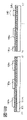
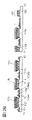
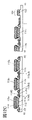
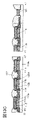
- FIG. 1A is a top view showing an example of a display device.
- FIG. 1B is a cross-sectional view showing an example of a display device; 2A to 2C are cross-sectional views showing examples of display devices. 3A to 3C are cross-sectional views showing examples of display devices. 4A to 4C are cross-sectional views showing examples of display devices. 5A and 5B are cross-sectional views showing an example of the display device. 6A and 6B are cross-sectional views showing an example of the display device. 7A to 7F are cross-sectional views showing examples of display devices. 8A to 8F are top views showing examples of pixels. 9A and 9B are top views illustrating an example of a method for manufacturing a display device.
- 10A to 10C are cross-sectional views illustrating an example of a method for manufacturing a display device.
- 11A to 11C are cross-sectional views illustrating an example of a method for manufacturing a display device.
- 12A to 12C are cross-sectional views illustrating an example of a method for manufacturing a display device.
- 13A to 13C are cross-sectional views illustrating an example of a method for manufacturing a display device.
- 14A to 14C are cross-sectional views illustrating an example of a method for manufacturing a display device.
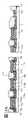
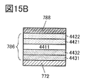
- 15A to 15F are diagrams showing configuration examples of light-emitting elements.
- FIG. 16 is a perspective view showing an example of a display device.
- FIG. 16 is a perspective view showing an example of a display device.
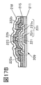
- 17A is a cross-sectional view showing an example of a display device
- 17B and 17C are cross-sectional views showing examples of transistors.
- FIG. 18 is a cross-sectional view showing an example of a display device.
- FIG. 19 is a cross-sectional view showing an example of a display device.
- FIG. 20 is a cross-sectional view showing an example of a display device.
- 21A to 21D are cross-sectional views showing examples of display devices.
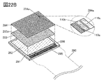
- 22A and 22B are perspective views showing an example of a display module.
- FIG. 23 is a cross-sectional view showing an example of a display device.
- FIG. 24 is a cross-sectional view showing an example of a display device.
- FIG. 25 is a cross-sectional view showing an example of a display device.
- FIG. 25 is a cross-sectional view showing an example of a display device.
- FIG. 26 is a cross-sectional view showing an example of a display device.
- FIG. 27 is a cross-sectional view showing an example of a display device.
- FIG. 28A is a block diagram showing an example of a display device.
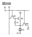
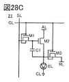
- 28B to 28D are diagrams showing examples of pixel circuits.
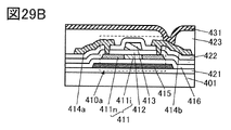
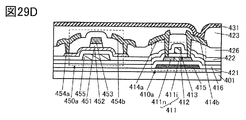
- 29A to 29D are cross-sectional views showing examples of transistors.
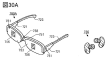
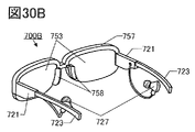
- 30A and 30B are diagrams illustrating examples of electronic devices.
- 31A and 31B are diagrams illustrating examples of electronic devices.
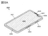
- FIG. 32A is a diagram illustrating an example of an electronic device;
- FIG. 32B is a cross-sectional view showing an example of electronic equipment.
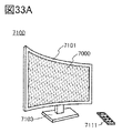
- 33A to 33D are diagrams showing examples of electronic devices.
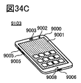
- 34A to 34G are diagrams showing examples of electronic devices.
- film and “layer” can be interchanged depending on the case or situation.
- conductive layer can be changed to the term “conductive film.”
- insulating film can be changed to the term “insulating layer”.
- an island-shaped light-emitting layer means that the light-emitting layer is physically separated from an adjacent light-emitting layer.
- parallel means, for example, a state in which two straight lines are arranged at an angle of -10° or more and 10° or less. Therefore, the case of ⁇ 5° or more and 5° or less is also included.
- perpendicular and perpendicular mean, for example, that two straight lines are arranged at an angle of 80° or more and 100° or less. Therefore, the case of 85° or more and 95° or less is also included.
- pixels are arranged in matrix in the display portion, and an image can be displayed on the display portion.
- the pixel has a plurality of subpixels exhibiting different emission colors, and the plurality of subpixels have different light emitting layers and a common layer provided in common. Having a common layer simplifies the manufacturing process and reduces manufacturing costs.
- a pixel indicates, for example, one element whose brightness can be controlled.
- one pixel indicates one color element, and the single color element expresses brightness.
- the minimum unit of an image is composed of three pixels: an R pixel, a G pixel, and a B pixel.
- each pixel of RGB can also be called a sub-pixel (sub-pixel), and three sub-pixels of RGB can be collectively called a pixel.
- a full-color display can be performed by using a light-emitting device corresponding to each color in a sub-pixel in each pixel.
- an OLED Organic Light Emitting Diode
- a QLED Quadantum-dot Light Emitting Diode
- the light-emitting substances possessed by the light-emitting device include substances that emit fluorescence (fluorescent materials), substances that emit phosphorescence (phosphorescent materials), inorganic compounds (quantum dot materials, etc.), and substances that exhibit heat-activated delayed fluorescence (heat-activated delayed fluorescence (Thermally Activated Delayed Fluorescence: TADF) material).
- the EL layer of the EL device has a light-emitting layer.
- the EL layer preferably has one or more of a hole-injection layer, a hole-transport layer, an electron-transport layer, and an electron-injection layer in addition to the light-emitting layer.
- the EL layer of each sub-pixel has a different light-emitting layer for each sub-pixel, and a part of the EL layer (a hole injection layer, a hole transport layer, an electron injection layer, an electron transport layer, etc.) is used as a common layer.
- the R sub-pixel has a first EL layer
- the G sub-pixel has a second EL layer
- the B sub-pixel has a third EL layer.
- the first light-emitting layer of the first EL layer, the second light-emitting layer of the second EL layer, and the third light-emitting layer of the third EL layer are formed using different materials.
- a part of the EL layer (a hole injection layer, a hole transport layer, an electron injection layer and an electron transport layer, etc.) can be made of the same material as a common layer.
- the EL layer may have a part of the EL layer (a hole-injection layer, a hole-transport layer, an electron-injection layer, an electron-transport layer, etc.) that is not formed as a common layer.
- the light-emitting device of each sub-pixel is formed by an EL device exhibiting a different emission color
- the light-emitting layer is formed in an island shape using a metal mask, and a part of the EL layer is formed.
- Hole-injection layer, hole-transport layer, electron-injection layer and electron-transport layer, etc. can be formed as a common layer.
- some of the layers included in the EL layer have relatively high conductivity, and when a layer with high conductivity is commonly provided for each pixel, leakage current may occur between pixels.
- the display device when a display device has a high definition or a high aperture ratio and the distance between pixels becomes small, the leakage current becomes unignorable, and there is a possibility that the display quality of the display device is deteriorated. Therefore, in the display device according to one embodiment of the present invention, at least part of the EL layer is formed in an island shape in each pixel, so that the display device has high definition and high reliability.
- a resist mask is formed at a position corresponding to each pixel, the conductive layer is processed into an island shape, and a first electrode (light-emitting electrode) is formed. (sometimes referred to as the lower electrode of the device) is formed. At this time, a step having a height T1 is generated in a region located between adjacent first electrodes. Next, part of the EL layer is formed over the entire surface. A part of the EL layer formed here can be called a first layer.
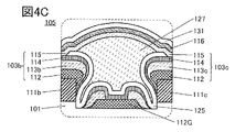
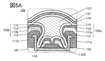
- T1/T2 is 0.5 or more, preferably 0.8 or more, more preferably 1 or more, more preferably 1.5 or more, and ⁇ is 60 degrees or more and 140 degrees or less, preferably 70 degrees or more and 140 degrees or less, more preferably 80 degrees or more and 140 degrees or less.
- the first layer preferably has a carrier-injection layer (hole-injection layer or electron-injection layer), and in addition to the carrier-injection layer, the carrier-transport layer (hole-transport layer or electron-transport layer) serves as a light-emitting layer. It is more preferable to have between
- the region where the upper layer is not formed on the side surface of the electrode formed in an island shape is sometimes called a discontinuous portion or a discontinuous region.
- the side surface of the first electrode has a region (stepped portion) where the first layer is not formed. may also have the effect of electrically isolating the first layer of each pixel. Therefore, it is not always necessary to have a region where the first layer is not formed on the side surface of the first electrode.
- a light-emitting layer is formed on the first layer of each pixel.
- a light-emitting layer that emits red light
- a light-emitting layer that emits blue light are formed.
- the light-emitting layer can be formed, for example, by vapor deposition using a metal mask.
- the light-emitting layer may have an island-like region on the side surface of the first electrode where the light-emitting layer is not formed, but the light-emitting layer may be formed.
- a region may be provided between adjacent first electrodes in which light-emitting layers exhibiting different emission colors overlap each other.
- a second layer is formed all over as part of the EL layer.
- the electron transport layer is formed as the second layer.
- a hole transport layer is formed as the second layer.
- the second layer may be separated into islands like the first layer, but may not be separated into islands.
- an insulating layer is formed over the entire surface. After that, the insulating layer is processed so as to leave the insulating layer in the concave portion between the adjacent first electrodes. At this time, the side surface of the first electrode may have a first region in direct contact with the first layer and a second region in direct contact with the insulating layer.
- the number of insulating layers may be one, but preferably two or more. When two or more insulating layers are provided, the insulating layer formed first can be designated as the first insulating layer, and the insulating layer formed next can be designated as the second insulating layer.
- a material with high solvent resistance, moisture barrier properties, and gas barrier properties as a material for the first insulating layer reduces damage to the EL layer during the manufacturing process of the display device. , the reliability of the light-emitting device can be enhanced.
- a liquid material is used in forming the second insulating layer, it becomes easier to fill recesses between adjacent pixels and obtain a flat shape.
- the insulating layer is removed at the position where the first electrode, first layer, light emitting layer, second layer, and insulating layer overlap to expose the second layer.
- a second electrode (sometimes referred to as an upper electrode of a light emitting element) is formed so as to be in contact with at least the exposed portions of the EL layers of all pixels.
- the second electrode can be formed without discontinuity in the concave portion between the adjacent pixels, and the discontinuity of the second electrode can be suppressed.
- a third layer may be formed before forming the second electrode.
- the third layer for example, an electron injection layer or a hole injection layer can be formed.
- an electron transport layer and an electron injection layer, or a hole transport layer and a hole injection layer may be formed.
- the first layer when the first layer is formed over the entire surface as part of the EL layer, the first layer serves as the lower electrode (first electrode). They are formed separately at positions in a self-aligned manner. Therefore, a light-emitting element capable of suppressing the occurrence of crosstalk can be obtained. In addition, it is possible to realize a high-definition display device or a display device with a high aperture ratio, which has been difficult to achieve. In addition, by filling recesses between adjacent pixels with an insulating layer, it is possible to suppress step disconnection defects when forming the upper electrode of the EL layer, and improve the productivity and reliability of the light-emitting device.
- the periphery of the EL layer that is not in contact with the upper electrode and the lower electrode is covered with a material having high solvent resistance, moisture barrier properties, and gas barrier properties. It is possible to reduce the damage to the EL layer in the first step and improve the reliability of the light-emitting device.
- a device manufactured using a metal mask or FMM may be referred to as a device with an MM (metal mask) structure.
- a device manufactured without using a metal mask or FMM may be referred to as a device with an MML (metal maskless) structure.
- the insulating layer also referred to as a protective insulating layer or a barrier layer
- the remaining layers for example, a carrier injection layer
- a common electrode which can also be called an upper electrode
- the carrier injection layer is often a layer with relatively high conductivity in the light-emitting device. Therefore, the light-emitting device may be short-circuited when the carrier injection layer comes into contact with the side surface of the island-shaped EL layer. Note that even in the case where the carrier injection layer is provided in an island shape and only the common electrode is formed in common among the light emitting devices, the common electrode and the side surface of the island-shaped EL layer or the side surface of the pixel electrode should be in contact with each other. and the light-emitting device may short out.
- the display device of one embodiment of the present invention includes insulating layers (the first insulating layer and the second insulation layer).
- the common electrode includes the carrier injection layer.
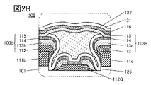
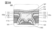
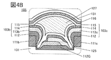
- a display device of one embodiment of the present invention includes a pixel electrode functioning as an anode; a hole-injection layer, a hole-transport layer, a light-emitting layer, and an electron-transport layer provided in this order over the pixel electrode; an insulating layer provided to cover each side surface of an electrode, a hole injection layer, a hole transport layer, a light emitting layer, and an electron transport layer; an electron injection layer provided on the electron transport layer; and a common electrode provided on the layer and functioning as a cathode.
- at least the pixel electrode and the hole injection layer are provided in an island shape.
- a display device of one embodiment of the present invention includes a pixel electrode functioning as a cathode, an electron-injection layer, an electron-transport layer, a light-emitting layer, and a hole-transport layer provided in this order over the pixel electrode; an insulating layer provided to cover side surfaces of the pixel electrode, the electron injection layer, the electron transport layer, the light emitting layer, and the hole transport layer; and the hole injection layer provided on the hole transport layer; and a common electrode provided on the hole injection layer and functioning as an anode.
- at least the pixel electrode and the electron injection layer are provided in an island shape.
- a display device of one embodiment of the present invention includes a pixel electrode, a first light-emitting unit over the pixel electrode, an intermediate layer (also referred to as a charge generation layer) over the first light-emitting unit, and a first light-emitting layer over the intermediate layer.
- a layer common to the light emitting devices of each color may be provided between the second light emitting unit and the common electrode.
- at least the pixel electrode and the first layer of the first light-emitting unit are provided in an island shape.
- a hole injection layer, an electron injection layer, or a charge generation layer is often a layer with relatively high conductivity among EL layers.
- the side surfaces of these layers are covered with the insulating layer; therefore, contact with a common electrode or the like can be suppressed. Therefore, short-circuiting of the light-emitting device can be suppressed, and the reliability of the light-emitting device can be improved.
- a display device of one embodiment of the present invention includes an insulating layer that covers a side surface of the pixel electrode, a side surface of the first layer, a side surface of the light-emitting layer, and a side surface of the second layer.
- the first layer can be formed separately in a self-aligned manner; It is a manufacturing method of the device.
- the insulating layer suppresses contact between the pixel electrode and the carrier injection layer or the common electrode, thereby suppressing short-circuiting of the light-emitting device.
- the insulating layer between adjacent pixel electrodes may have a single-layer structure or a laminated structure.
- the first insulating layer is formed in contact with the EL layer, it is preferably formed using an inorganic insulating material.
- ALD atomic layer deposition
- the inorganic insulating layer is formed using a sputtering method, a chemical vapor deposition (CVD) method, or a plasma enhanced CVD (PECVD) method, which has a higher film formation rate than the ALD method. preferably formed. Accordingly, a highly reliable display device can be manufactured with high productivity.
- the second insulating layer is preferably formed using an organic material so as to planarize the concave portion between adjacent pixels.
- an aluminum oxide film formed by an ALD method can be used for the first insulating layer, and a photosensitive organic resin film can be used for the second insulating layer.
- [Configuration example 1 of display device] 1A and 1B show a display device of one embodiment of the present invention.
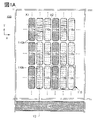
- FIG. 1A A top view of the display device 100 is shown in FIG. 1A.
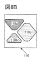
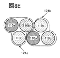
- the display device 100 has a display section in which a plurality of pixels 110 are arranged in a matrix, and a connection section 140 outside the display section.
- a stripe arrangement is applied to the pixels 110 shown in FIG. 1A.
- the pixel 110 shown in FIG. 1A is composed of three sub-pixels, sub-pixels 110a, 110b, and 110c.
- the sub-pixels 110a, 110b, and 110c include a light-emitting device 130a that emits red light, a light-emitting device 130b that emits green light, and a light-emitting device 130c that emits blue light (hereinafter sometimes collectively referred to as light-emitting devices 130). .
- FIG. 1B shows a cross-sectional view between the dashed-dotted line X1-X2 in FIG. 1A.
- the sub-pixel 110a, sub-pixel 110b, and sub-pixel 110c have a light-emitting device 130a that emits red light, a light-emitting device 130b that emits green light, and a light-emitting device 130c that emits blue light.
- the configuration of the sub-pixels 110a, 110b, and 110c is not limited to the three colors of red (R), green (G), and blue (B), but also yellow (Y), cyan (C), and magenta (M). Sub-pixels of three colors may also be used.
- FIG. 1A shows an example in which sub-pixels of different colors are arranged side by side in the X direction and sub-pixels of the same color are arranged side by side in the Y direction. Sub-pixels of different colors may be arranged side by side in the Y direction, and sub-pixels of the same color may be arranged side by side in the X direction.
- FIG. 1A shows an example in which the connecting portion 140 is positioned below the display portion when viewed from the top
- the connecting portion 140 may be provided in at least one position on the upper side, the right side, the left side, or the lower side of the display portion when viewed from above, and may be provided so as to surround the four sides of the display portion.
- the number of connection parts 140 may be singular or plural.
- the display device 100 includes light emitting devices 130a, 130b, and 130c provided on a layer 101 including transistors, and a protective layer 131 covering these light emitting devices.
- a display device of one embodiment of the present invention is a top emission type in which light is emitted in a direction opposite to a substrate over which a light-emitting device is formed, and light is emitted toward a substrate over which a light-emitting device is formed.
- a bottom emission type bottom emission type
- a double emission type dual emission type in which light is emitted from both sides may be used.
- the layer 101 including transistors for example, a stacked structure in which a plurality of transistors are provided on a substrate and an insulating layer is provided to cover these transistors can be applied.
- the layer 101 containing transistors may have recesses between adjacent light emitting devices.
- recesses may be provided in the insulating layer located on the outermost surface of the layer 101 including the transistor.
- FIG. 3 A structural example of the layer 101 including a transistor will be described later in Embodiments 3 and 4.
- a light-emitting device has an EL layer between a pair of electrodes.
- one of a pair of electrodes may be referred to as a pixel electrode and the other may be referred to as a common electrode.
- one electrode functions as an anode and the other electrode functions as a cathode.
- the pixel electrode functions as an anode and the common electrode functions as a cathode will be described below as an example.
- the light-emitting device 130a includes a pixel electrode 111a on the layer 101 including a transistor, an island-shaped first layer 112 on the pixel electrode 111a, a first light-emitting layer 113a on the first layer 112, and a first light-emitting layer 113a on the pixel electrode 111a. It has a second layer 114 on the light-emitting layer 113 a , a third layer 115 on the second layer 114 , and a common electrode 116 on the third layer 115 .
- first layer 112, first light-emitting layer 113a, second layer 114, and third layer 115 can be collectively referred to as EL layer 103a. Note that a configuration example of the light-emitting device will be described later in Embodiment Mode 2.
- the light-emitting device 130b includes a pixel electrode 111b on the layer 101 including a transistor, an island-shaped first layer 112 on the pixel electrode 111b, a second light-emitting layer 113b on the first layer 112, and a second light-emitting layer 113b on the pixel electrode 111b. It has a second layer 114 on the light-emitting layer 113 b , a third layer 115 on the second layer 114 , and a common electrode 116 on the third layer 115 .
- first layer 112, second light-emitting layer 113b, second layer 114, and third layer 115 can be collectively referred to as EL layer 103b.
- the light-emitting device 130c includes a pixel electrode 111c on the layer 101 including a transistor, an island-shaped first layer 112 on the pixel electrode 111c, a third light-emitting layer 113c on the first layer 112, and a third layer 113c on the pixel electrode 111c. It has a second layer 114 over the light-emitting layer 113 c , a third layer 115 over the second layer 114 , and a common electrode 116 over the third layer 115 .
- first layer 112, third light-emitting layer 113c, second layer 114, and third layer 115 can be collectively referred to as EL layer 103c.
- the EL layer 103a of the light emitting device 130a, the EL layer 103b of the light emitting device 130b, and the EL layer 103c of the light emitting device 130c are sometimes collectively called the EL layer 103.
- the first light-emitting layer 113a of the light-emitting device 130a, the second light-emitting layer 113b of the light-emitting device 130b, and the third light-emitting layer 113c of the light-emitting device 130c are collectively referred to as the light-emitting layer 113
- the light-emitting layer 113 There is
- the same film is shared as the common electrode 116 in each color light-emitting device.
- a common electrode that each light emitting device has in common is electrically connected to a conductive layer provided in the connecting portion 140 .
- the common electrodes of the light emitting devices have the same potential.
- a conductive film that transmits visible light is used for the electrode on the light extraction side of the pixel electrode and common electrode.
- a conductive film that reflects visible light is preferably used for the electrode on the side from which light is not extracted.
- indium tin oxide also referred to as In—Sn oxide, ITO
- In—Si—Sn oxide also referred to as ITSO
- indium zinc oxide In—Zn oxide
- In—W— Zn oxides aluminum-containing alloys (aluminum alloys) such as alloys of aluminum, nickel, and lanthanum (Al-Ni-La)
- Al-Ni-La aluminum-containing alloys
- Al-Ni-La aluminum-containing alloys
- alloys of silver, palladium and copper Ag-Pd-Cu, also referred to as APC
- elements belonging to Group 1 or Group 2 of the periodic table of elements not exemplified above e.g., lithium (Li), cesium (Cs), calcium (Ca), strontium (Sr)), europium (Eu), ytterbium
- Yb rare earth metal
- an alloy containing an appropriate combination thereof, graphene, or the like can be used.
- a micro optical resonator (microcavity) structure is preferably applied to the light emitting device. Therefore, one of the pair of electrodes of the light-emitting device preferably has an electrode (semi-transmissive/semi-reflective electrode) that is transparent and reflective to visible light, and the other is an electrode that is reflective to visible light ( reflective electrode). Since the light-emitting device has a microcavity structure, the light emitted from the light-emitting layer can be resonated between both electrodes, and the light emitted from the light-emitting device can be enhanced.
- the semi-transmissive/semi-reflective electrode can have a laminated structure of a reflective electrode and an electrode having transparency to visible light (also referred to as a transparent electrode).
- the light transmittance of the transparent electrode is set to 40% or more.
- the light-emitting device preferably uses an electrode having a transmittance of 40% or more for visible light (light with a wavelength of 400 nm or more and less than 750 nm).
- the visible light reflectance of the semi-transmissive/semi-reflective electrode is 10% or more and 95% or less, preferably 30% or more and 80% or less.
- the visible light reflectance of the reflective electrode is 40% or more and 100% or less, preferably 70% or more and 100% or less.
- the resistivity of these electrodes is preferably 1 ⁇ 10 ⁇ 2 ⁇ cm or less.
- the first layer 112 is provided in an island shape on the pixel electrode 111 (111a, 111b, 111c) of each pixel.
- the EL layer 103a, the EL layer 103b, and the EL layer 103c each have a light-emitting layer 113 (113a, 113b, 113c).
- a light-emitting layer is a layer containing a light-emitting substance.
- the emissive layer can have one or more emissive materials. Examples of light-emitting substances include fluorescent materials, phosphorescent materials, TADF materials, and quantum dot materials.
- fluorescent materials include pyrene derivatives, anthracene derivatives, triphenylene derivatives, fluorene derivatives, carbazole derivatives, dibenzothiophene derivatives, dibenzofuran derivatives, dibenzoquinoxaline derivatives, quinoxaline derivatives, pyridine derivatives, pyrimidine derivatives, phenanthrene derivatives, and naphthalene derivatives. be done.
- Examples of phosphorescent materials include organometallic complexes (especially iridium complexes) having a 4H-triazole skeleton, 1H-triazole skeleton, imidazole skeleton, pyrimidine skeleton, pyrazine skeleton, or pyridine skeleton, and phenylpyridine derivatives having an electron-withdrawing group.
- organometallic complexes especially iridium complexes
- platinum complexes, rare earth metal complexes, etc. which are used as ligands, can be mentioned.
- the light-emitting layer may contain one or more organic compounds (host material, assist material, etc.) in addition to the light-emitting substance (guest material).
- One or both of a hole-transporting material and an electron-transporting material can be used as the one or more organic compounds.
- Bipolar materials or TADF materials may also be used as one or more organic compounds.
- the light-emitting layer preferably includes, for example, a phosphorescent material and a combination of a hole-transporting material and an electron-transporting material that easily form an exciplex.
- ExTET Exciplex-Triplet Energy Transfer
- a combination that forms an exciplex that emits light that overlaps with the wavelength of the absorption band on the lowest energy side of the light-emitting substance energy transfer becomes smooth and light emission can be efficiently obtained. With this configuration, high efficiency, low-voltage driving, and long life of the light-emitting device can be realized at the same time.
- the EL layer 103a, the EL layer 103b, and the EL layer 103c include, as layers other than the light-emitting layer, a substance with a high hole-injection property, a substance with a high hole-transport property, a hole-blocking material, a substance with a high electron-transport property, A layer containing a highly electron-injecting substance, an electron-blocking material, a bipolar substance (a substance with high electron-transporting and hole-transporting properties), or the like may be further included.
- Both low-molecular-weight compounds and high-molecular-weight compounds can be used in the light-emitting device, and inorganic compounds may be included.
- Each of the layers constituting the light-emitting device can be formed by a vapor deposition method (including a vacuum vapor deposition method), a sputtering method, a printing method, an inkjet method, a coating method, or the like.
- the first layer 112 may have a hole injection layer or an electron injection layer.
- the first layer 112 may further have a hole transport layer or an electron transport layer in addition to the hole injection layer or the electron injection layer.
- the first layer 112 when the pixel electrode 111 is the anode, can be a hole injection layer or a hole injection layer and a hole transport layer.
- the first layer 112 when the pixel electrode 111 is used as a cathode can be an electron injection layer or an electron injection layer and an electron transport layer.
- each of the light-emitting layers 113 has a carrier transport layer as the second layer 114 on the light-emitting layer 113 . Accordingly, exposure of the light-emitting layer 113 to the outermost surface can be suppressed during the manufacturing process of the display device 100, and damage to the light-emitting layer 113 can be reduced. This can improve the reliability of the light emitting device.
- the second layer 114 can be an electron transport layer when the pixel electrode 111 is the anode. Further, for example, the second layer 114 when the pixel electrode 111 is used as a cathode can be a hole transport layer.
- a carrier injection layer may be formed as the third layer 115 on the second layer 114 of the EL layer 103 .
- the third layer 115 can be an electron injection layer when the pixel electrode 111 is the anode.
- the third layer 115 when the pixel electrode 111 is used as a cathode can be a hole injection layer.
- the hole-injecting layer is a layer that injects holes from the anode into the hole-transporting layer, and contains a material with high hole-injecting properties.
- highly hole-injecting materials include aromatic amine compounds and composite materials containing a hole-transporting material and an acceptor material (electron-accepting material).
- the hole-transporting layer is a layer that transports holes injected from the anode to the light-emitting layer by means of the hole-injecting layer.
- a hole-transporting layer is a layer containing a hole-transporting material.
- a substance having a hole mobility of 10 ⁇ 6 cm 2 /Vs or more is preferable as the hole-transporting material. Note that substances other than these can be used as long as they have a higher hole-transport property than electron-transport property.
- hole-transporting materials include ⁇ -electron-rich heteroaromatic compounds (e.g., carbazole derivatives, thiophene derivatives, furan derivatives, etc.), aromatic amines (compounds having an aromatic amine skeleton), and other highly hole-transporting materials. is preferred.
- ⁇ -electron-rich heteroaromatic compounds e.g., carbazole derivatives, thiophene derivatives, furan derivatives, etc.
- aromatic amines compounds having an aromatic amine skeleton
- other highly hole-transporting materials is preferred.
- the electron-transporting layer is a layer that transports electrons injected from the cathode to the light-emitting layer by the electron-injecting layer.
- the electron-transporting layer is a layer containing an electron-transporting material.
- an electron-transporting material a substance having an electron mobility of 1 ⁇ 10 ⁇ 6 cm 2 /Vs or more is preferable. Note that substances other than these substances can be used as long as they have a higher electron-transport property than hole-transport property.
- electron-transporting materials include metal complexes having a quinoline skeleton, metal complexes having a benzoquinoline skeleton, metal complexes having an oxazole skeleton, metal complexes having a thiazole skeleton, oxadiazole derivatives, triazole derivatives, imidazole derivatives, ⁇ electron deficient including oxazole derivatives, thiazole derivatives, phenanthroline derivatives, quinoline derivatives with quinoline ligands, benzoquinoline derivatives, quinoxaline derivatives, dibenzoquinoxaline derivatives, pyridine derivatives, bipyridine derivatives, pyrimidine derivatives, and other nitrogen-containing heteroaromatic compounds
- a material having a high electron transport property such as a type heteroaromatic compound can be used.
- the electron-transporting layer may have a laminated structure, and has a hole-blocking layer in contact with the light-emitting layer for blocking holes from moving from the anode side to the cathode side through the light-emitting layer. It's okay to be
- the electron injection layer is a layer that injects electrons from the cathode to the electron transport layer, and is a layer that contains a material with high electron injection properties.
- Alkali metals, alkaline earth metals, or compounds thereof can be used as materials with high electron injection properties.
- a composite material containing an electron-transporting material and a donor material (electron-donating material) can also be used as a material with high electron-injecting properties.
- the electron injection layer examples include lithium, cesium, ytterbium, lithium fluoride (LiF), cesium fluoride (CsF), calcium fluoride (CaF x , X is an arbitrary number), and 8-(quinolinolato)lithium (abbreviation: Liq), 2-(2-pyridyl)phenoratritium (abbreviation: LiPP), 2-(2-pyridyl)-3-pyridinolatritium (abbreviation: LiPPy), 4-phenyl-2-(2-pyridyl)pheno Latritium (abbreviation: LiPPP), lithium oxide (LiO x , X is an arbitrary number), alkali metals such as cesium carbonate, alkaline earth metals, or compounds thereof can be used.
- the electron injection layer may have a laminated structure of two or more layers. As the laminated structure, for example, lithium fluoride can be used for the first layer and ytterbium can be used
- an electron-transporting material may be used as the electron injection layer.
- a compound having a lone pair of electrons and an electron-deficient heteroaromatic ring can be used as the electron-transporting material.
- a compound having at least one of a pyridine ring, diazine ring (pyrimidine ring, pyrazine ring, pyridazine ring), and triazine ring can be used.
- the lowest unoccupied molecular orbital (LUMO) level of the organic compound having an unshared electron pair is preferably -3.6 eV or more and -2.3 eV or less.
- CV cyclic voltammetry
- photoelectron spectroscopy optical absorption spectroscopy
- inverse photoelectron spectroscopy etc. are used to determine the highest occupied molecular orbital (HOMO: Highest Occupied Molecular Orbital) level and LUMO level of an organic compound. can be estimated.
- BPhen 4,7-diphenyl-1,10-phenanthroline
- NBPhen 2,9-di(naphthalen-2-yl)-4,7-diphenyl-1,10-phenanthroline
- HATNA diquinoxalino [2,3-a:2′,3′-c]phenazine
- TmPPPyTz 2,4,6-tris[3′-(pyridin-3-yl)biphenyl-3-yl]-1,3 , 5-triazine
- an intermediate layer is provided between the two light-emitting units.
- the intermediate layer has a function of injecting electrons into one of the two light-emitting units and holes into the other when a voltage is applied between the pair of electrodes.
- a material that can be applied to an electron injection layer such as lithium
- a material applicable to the hole injection layer can be preferably used.
- a layer containing a hole-transporting material and an acceptor material can be used for the intermediate layer.
- a layer containing an electron-transporting material and a donor material can be used for the intermediate layer.
- the side surfaces of the plurality of light-emitting units and the intermediate layers included in these layers are also covered with the insulating layers 125 and 127. . This prevents the third layer 115 (and/or the common electrode 116) from coming into contact with any side surface of the plurality of light emitting units and the intermediate layer, thereby suppressing short circuits in the light emitting device.
- the insulating layer 125 preferably covers at least the side surfaces of the pixel electrodes 111 . Furthermore, the insulating layer 125 preferably covers the side surfaces of the first layer 112 , the light emitting layer 113 and the second layer 114 . The insulating layer 125 can be in contact with one or more side surfaces of the pixel electrode 111 and the second layer 114 .
- the insulating layer 125 is preferably an insulating layer containing an inorganic material.
- the insulating layer 127 is provided on the insulating layer 125 so as to fill the recesses formed in the insulating layer 125 .
- the insulating layer 127 can overlap with side surfaces of the pixel electrode 111, the first layer 112, the light-emitting layer 113, and the second layer 114 with the insulating layer 125 interposed therebetween.
- the insulating layer 127 is preferably an insulating layer containing an organic material.
- the insulating layer 125 is arranged below the insulating layer 127, and the organic layer 112G and the like are arranged below the insulating layer 125. As shown in FIG. By including the organic layer 112G and the like, the shape of the insulating layer 127 after filling can be made flatter in some cases.
- one of the insulating layer 125 and the insulating layer 127 may not be provided.
- the insulating layer 127 can be in contact with at least part of the side surface of the EL layer 103 .
- the number of steps for manufacturing the display device can be reduced.
- the insulating layer 125 containing an inorganic material in contact with the side surfaces of the first layer 112, the light-emitting layer 113, and/or the second layer 114 the effect of suppressing contamination of these layers with impurities is enhanced. can be done.
- the planarity of the surface on which the third layer 115 and the common electrode 116 are formed can be improved.
- the third layer 115 and the common electrode 116 are provided on the second layer 114 , the insulating layer 125 and the insulating layer 127 .
- the steps can be planarized, and coverage with the third layer 115 and the common electrode 116 can be improved. Therefore, it is possible to suppress poor connection due to step disconnection of the common electrode 116 .
- the common electrode 116 including the third layer 115 may be called.
- the top surface of the insulating layer 125 and the top surface of the insulating layer 127 are adjusted to the heights of the first layer 112, the light-emitting layer 113, and the top surface of the insulating layer 127, respectively. , preferably matches or approximately matches the height of the top surface of at least one of the second layers 114 .
- the upper surface of the insulating layer 127 preferably has a flat shape, and may have a convex portion or a concave portion.
- the insulating layer 125 has a region in contact with one or more side surfaces of the first layer 112, the light-emitting layer 113, and the second layer 114, and the first layer 112, the light-emitting layer 113, and the second layer 114. It functions as a protective insulating layer for the second layer 114 .
- impurities oxygen, moisture, or the like
- highly reliable display can be achieved. can be a device.
- the width (thickness) of the insulating layer 125 in a region in contact with one or more side surfaces of the first layer 112, the light-emitting layer 113, and the second layer 114 in a cross-sectional view is large, the width (thickness) of the insulating layer 125 is large. 112, the light-emitting layer 113, and the second layer 114, and the aperture ratio may decrease.
- the width (thickness) of the insulating layer 125 is small, the effect of suppressing the intrusion of impurities from the side surfaces of the first layer 112, the light emitting layer 113, and the second layer 114 is reduced. may be lost.
- the width (thickness) of the insulating layer 125 in the region in contact with one or more side surfaces of the first layer 112, the light-emitting layer 113, and the second layer 114 is preferably 3 nm or more and 200 nm or less. It is preferably 3 nm or more and 150 nm or less, more preferably 5 nm or more and 150 nm or less, further preferably 5 nm or more and 100 nm or less, further preferably 10 nm or more and 100 nm or less, further preferably 10 nm or more and 50 nm or less.
- the insulating layer 125 can be an insulating layer having an inorganic material.
- an inorganic insulating film such as an oxide insulating film, a nitride insulating film, an oxynitride insulating film, or a nitride oxide insulating film can be used, for example.
- the insulating layer 125 may have a single-layer structure or a laminated structure.
- the oxide insulating film includes a silicon oxide film, an aluminum oxide film, a magnesium oxide film, an indium gallium zinc oxide film, a gallium oxide film, a germanium oxide film, an yttrium oxide film, a zirconium oxide film, a lanthanum oxide film, a neodymium oxide film, and an oxide film.
- Examples include a hafnium film and a tantalum oxide film.
- Examples of the nitride insulating film include a silicon nitride film and an aluminum nitride film.
- As the oxynitride insulating film a silicon oxynitride film, an aluminum oxynitride film, or the like can be given.
- nitride oxide insulating film a silicon nitride oxide film, an aluminum nitride oxide film, or the like can be given.
- aluminum oxide is preferable because it has a high etching selectivity with respect to the EL layer and has a function of protecting the EL layer during formation of the insulating layer 127 described later.
- an inorganic insulating film such as an aluminum oxide film, a hafnium oxide film, or a silicon oxide film formed by an ALD method to the insulating layer 125, the insulating layer 125 with few pinholes and an excellent function of protecting the EL layer can be obtained. can be formed.
- an oxynitride insulator refers to a material whose composition contains more oxygen than nitrogen
- a nitride oxide insulator refers to a material whose composition contains more nitrogen than oxygen. refers to materials with a high
- silicon oxynitride refers to a material whose composition contains more oxygen than nitrogen
- silicon nitride oxide refers to a material whose composition contains more nitrogen than oxygen.
- a sputtering method, a CVD method, a PLD method, an ALD method, or the like can be used to form the insulating layer 125 .
- the insulating layer 125 is preferably formed by an ALD method with good coverage.
- the insulating layer 127 provided on the insulating layer 125 has the function of flattening the recesses of the insulating layer 125 formed between adjacent light emitting devices. In other words, the presence of the insulating layer 127 has the effect of improving the flatness of the surface on which the common electrode 116 is formed.
- an insulating layer containing an organic material can be preferably used.
- acrylic resin, polyimide resin, epoxy resin, imide resin, polyamide resin, polyimideamide resin, silicone resin, siloxane resin, benzocyclobutene-based resin, phenolic resin, and precursors of these resins are applied. can do.
- an organic material such as polyvinyl alcohol (PVA), polyvinyl butyral, polyvinylpyrrolidone, polyethylene glycol, polyglycerin, pullulan, water-soluble cellulose, or alcohol-soluble polyamide resin may be used for the insulating layer 127 .
- a photosensitive resin can be used as the insulating layer 127 .
- a photoresist may be used as the photosensitive resin.
- a positive material or a negative material can be used for the photosensitive resin.
- the difference between the height of the upper surface of the insulating layer 127 and the height of the upper surface of the second layer 114 is preferably, for example, 0.5 times or less, more preferably 0.3 times or less, the thickness of the insulating layer 127 .
- the insulating layer 127 may be provided so that the top surface of the second layer 114 is higher than the top surface of the insulating layer 127 .
- the insulating layer 127 may be provided so that the top surface of the insulating layer 127 is lower than the top surface of the second layer 114 .
- a protective layer 131 on the light emitting devices 130a, 130b, 130c.
- the reliability of the light-emitting device can be improved.
- the protective layer 131 may be composed of multiple layers. For example, it may have a two-layer structure of an inorganic layer and an inorganic layer, a two-layer structure of an inorganic layer and an organic layer, or a three-layer structure of an inorganic layer, an organic layer and an inorganic layer.
- the conductivity of the protective layer 131 does not matter. At least one of an insulating film, a semiconductor film, and a conductive film can be used as the protective layer 131 .
- the protective layer 131 has an inorganic film, deterioration of the light-emitting devices is suppressed, such as preventing oxidation of the common electrode 116 and suppressing impurities (moisture, oxygen, etc.) from entering the light-emitting devices 130a, 130b, and 130c. Therefore, the reliability of the display device can be improved.
- inorganic insulating films such as an oxide insulating film, a nitride insulating film, an oxynitride insulating film, and a nitride oxide insulating film can be used.
- oxide insulating film include a silicon oxide film, an aluminum oxide film, a gallium oxide film, a germanium oxide film, an yttrium oxide film, a zirconium oxide film, a lanthanum oxide film, a neodymium oxide film, a hafnium oxide film, a tantalum oxide film, and the like.
- nitride insulating film examples include a silicon nitride film and an aluminum nitride film.
- oxynitride insulating film a silicon oxynitride film, an aluminum oxynitride film, or the like can be given.
- nitride oxide insulating film a silicon nitride oxide film, an aluminum nitride oxide film, or the like can be given.
- the protective layer 131 preferably has a nitride insulating film or a nitride oxide insulating film, and more preferably has a nitride insulating film.
- the protective layer 131 includes In—Sn oxide (also referred to as ITO), In—Zn oxide, Ga—Zn oxide, Al—Zn oxide, or indium gallium zinc oxide (In—Ga—Zn oxide).
- Inorganic films containing materials such as IGZO can also be used.
- the inorganic film preferably has a high resistance, and more specifically, preferably has a higher resistance than the common electrode 116 .
- the inorganic film may further contain nitrogen.
- the protective layer 131 When the light emitted from the light-emitting device is taken out through the protective layer 131, the protective layer 131 preferably has high transparency to visible light.
- the protective layer 131 preferably has high transparency to visible light.
- ITO, IGZO, and aluminum oxide are preferable because they are inorganic materials with high transparency to visible light.
- the protective layer 131 for example, a stacked structure of an aluminum oxide film and a silicon nitride film over the aluminum oxide film, or a stacked structure of an aluminum oxide film and an IGZO film over the aluminum oxide film, or the like can be used. can be done. By using the stacked structure, impurities (such as water and oxygen) entering the EL layer can be suppressed.
- the protective layer 131 may have an organic film.
- protective layer 131 may have both an organic film and an inorganic film.
- the protective layer 131 may be formed using a plurality of different film formation methods. Specifically, the first layer of the protective layer 131 may be formed using an atomic layer deposition method, and the second layer of the protective layer 131 may be formed using a sputtering method.
- a light shielding layer may be provided at a position overlapping the insulating layer between pixels.
- various optical members can be arranged at positions overlapping with the light emitting device. Examples of optical members include polarizing plates, retardation plates, light diffusion layers (diffusion films, etc.), antireflection layers, light collecting films, and the like.
- an antistatic film that suppresses the adhesion of dust, a water-repellent film that prevents the adhesion of dirt, a hard coat film that suppresses the occurrence of scratches due to use, and a shock-absorbing layer are placed on the outside of the display device.
- a substrate may be provided on the protective layer 131 via a resin layer.
- Glass, quartz, ceramic, sapphire, resin, metal, alloy, semiconductor, or the like can be used for the substrate.
- a material that transmits the light is used for the substrate on the side from which the light from the light-emitting device is extracted.
- a polarizing plate may also be used as the substrate.
- polyester resins such as polyethylene terephthalate (PET) and polyethylene naphthalate (PEN), polyacrylonitrile resins, acrylic resins, polyimide resins, polymethyl methacrylate resins, polycarbonate (PC) resins, and polyethersulfone (PES) are used.
- Resin, polyamide resin (nylon, aramid, etc.), polysiloxane resin, cycloolefin resin, polystyrene resin, polyamideimide resin, polyurethane resin, polyvinyl chloride resin, polyvinylidene chloride resin, polypropylene resin, polytetrafluoroethylene (PTFE) resin , ABS resin, cellulose nanofiber, and the like can be used.
- a glass having a thickness that is flexible may be used for the substrate.
- a substrate having high optical isotropy has small birefringence (it can be said that the amount of birefringence is small).
- the absolute value of the retardation (retardation) value of the substrate with high optical isotropy is preferably 30 nm or less, more preferably 20 nm or less, and even more preferably 10 nm or less.
- Films with high optical isotropy include triacetyl cellulose (TAC, also called cellulose triacetate) films, cycloolefin polymer (COP) films, cycloolefin copolymer (COC) films, and acrylic films.
- TAC triacetyl cellulose
- COP cycloolefin polymer
- COC cycloolefin copolymer
- a film having a low water absorption rate as the substrate.
- various curing adhesives such as UV curing adhesives, reaction curing adhesives, thermosetting adhesives, and anaerobic adhesives can be used.
- These adhesives include epoxy resins, acrylic resins, silicone resins, phenol resins, polyimide resins, imide resins, PVC (polyvinyl chloride) resins, PVB (polyvinyl butyral) resins, EVA (ethylene vinyl acetate) resins, and the like.
- a material with low moisture permeability such as epoxy resin is preferable.
- a two-liquid mixed type resin may be used.
- an adhesive sheet or the like may be used.
- materials that can be used for conductive layers such as various wirings and electrodes constituting display devices include aluminum, titanium, chromium, nickel, copper, yttrium, zirconium, molybdenum, silver, Examples include metals such as tantalum and tungsten, and alloys containing these metals as main components. A film containing these materials can be used as a single layer or as a laminated structure.
- conductive oxides such as indium oxide, indium tin oxide, indium zinc oxide, zinc oxide, zinc oxide containing gallium, or graphene can be used.
- metal materials such as gold, silver, platinum, magnesium, nickel, tungsten, chromium, molybdenum, iron, cobalt, copper, palladium, and titanium, or alloy materials containing such metal materials can be used.
- a nitride of the metal material eg, titanium nitride
- it is preferably thin enough to have translucency.
- a stacked film of any of the above materials can be used as the conductive layer.
- a laminated film of a silver-magnesium alloy and indium tin oxide because the conductivity can be increased.
- conductive layers such as various wirings and electrodes that constitute a display device, and conductive layers (conductive layers functioning as pixel electrodes or common electrodes) of light-emitting devices.
- Examples of insulating materials that can be used for each insulating layer include resins such as acrylic resins and epoxy resins, and inorganic insulating materials such as silicon oxide, silicon oxynitride, silicon nitride oxide, silicon nitride, and aluminum oxide.
- FIG. 2 to 5 show the detailed structure and the structure of the modified example by enlarging the region 105 surrounded by the dashed line in FIG. 1B.
- FIG. 2A is an enlarged view of region 105 in FIG. 1B.
- the pixel electrode 111 (111b, 111c) has a region in contact with the first layer 112 and a region in contact with the insulating layer 125 on the side surface.
- the pixel electrode 111 (111b, 111c) may have a region in contact with the light-emitting layer 113 (113b, 113c) and/or a region in contact with the second layer 114 on the side surface.
- an organic layer 112G, an organic layer 113bG, an organic layer 113cG, and an organic layer 114G are provided between adjacent pixel electrodes.
- each of the first layer 112, the light-emitting layers 113 (113b and 113c), and the second layer 114 has a region covered with the insulating layer 125 between adjacent pixel electrodes.
- An insulating layer 127 is provided over the insulating layer 125 between adjacent pixel electrodes.
- the insulating layer 127 is preferably provided so as to fill the concave portion between adjacent pixel electrodes.
- the insulating layer 127 may have a curved convex portion between adjacent pixel electrodes, and the end portion of the insulating layer 125 may have a forward taper.
- FIG. 2A shows an example in which the upper surface of the insulating layer 127 is an arcuate protrusion in a cross-sectional view, but as shown in FIG. There may be.
- FIG. 2A shows a configuration in which the insulating layer 125 is provided
- the present invention is not limited to this.
- FIG. 2C is a variation of the structure shown in FIG. 2A.
- a structure without the insulating layer 125 may be employed as shown in FIG. 2C.
- the insulating layer 127 is preferably made of an organic material that causes less damage to the first layer 112, the light-emitting layer 113, and the second layer 114.
- FIG. 2C shows a structure in which the insulating layer 125 is provided, the present invention is not limited to this.
- FIG. 2C is a variation of the structure shown in FIG. 2A.
- a structure without the insulating layer 125 may be employed as shown in FIG. 2C.
- the insulating layer 127 is preferably made of an organic material that causes less damage to the first layer 112, the light-emitting layer 113, and the second layer 114.
- the insulating layer 127 is preferably made of an organic material such as polyvinyl alcohol (PVA), polyvinyl butyral, polyvinylpyrrolidone, polyethylene glycol, polyglycerin, pullulan, water-soluble cellulose, or alcohol-soluble polyamide resin.
- PVA polyvinyl alcohol
- polyvinyl butyral polyvinylpyrrolidone
- polyethylene glycol polyglycerin
- pullulan polyethylene glycol
- polyglycerin polyglycerin
- pullulan polyethylene glycol
- pullulan polyglycerin
- water-soluble cellulose water-soluble cellulose
- alcohol-soluble polyamide resin alcohol-soluble polyamide resin
- the shape of the insulating layer 127 of one embodiment of the present invention is described using the width W1 of the first portion and the width W2 of the second portion indicated by double arrows in FIG. 2C.
- the insulating layer 127 has a first portion located between the pair of pixel electrodes and a second portion located between the pair of EL layers, and the width W2 of the second portion is equal to that of the first portion. It can be said that the shape is narrower than the width W1.
- FIGS. 2A, 2B, 3A-3C, 4A-4C, 5A and 5B do not show the width W1 of the first portion and the width W2 of the second portion, but are similar to FIG. 2C.
- the insulating layer 127 has a first portion located between the pair of pixel electrodes and a second portion located between the pair of EL layers, and the width W2 of the second portion is the width of the first portion. It can be said that the shape is narrower than the width W1 of the portion.
- the insulating layer 127 having a shape in which the width W2 of the second portion is narrower than the width W1 of the first portion is also said to have a constricted shape in a cross-sectional view.
- FIG. 2A and the like show a configuration in which the top surfaces of the insulating layers 125 and 127 are higher than the top surface of the second layer 114
- the present invention is limited to this. not a thing
- the top surface of the insulating layer 125 and the top surface of the insulating layer 127 are at least one of the top surface of the first layer 112, the top surface of the light-emitting layer 113, and the second layer 114. It may be configured to substantially match the top surface of the two.
- FIG. 2A and the like show an example of a structure in which the layer 101 is cut between adjacent pixel electrodes 111 (a structure in which the layer 101 has a concave portion between adjacent pixel electrodes 111).
- the structure is not limited to this, and a structure in which the layer 101 is not shaved between the adjacent pixel electrodes 111 (a structure in which the layer 101 does not have recesses between the adjacent pixel electrodes 111, or a structure in which the layer 101 does not have a concave portion between the adjacent pixel electrodes 111) layer 101 may be a flat structure).
- the structure in which the layer 101 is removed between the adjacent pixel electrodes 111 can also be said to have a stepped portion in the layer 101 between the adjacent pixel electrodes 111 . It says.
- the insulating layer 127 may have a recess that is lower than the top surface of at least one of the first layer 112, the light-emitting layer 113, and the second layer 114. However, it is desirable that the third layer 115 and the common electrode 116 are not interrupted in the recess.
- the side surface of the pixel electrode 111 has a region where the first layer 112 is not formed.
- the effect of electrically isolating the light-emitting layer may be obtained. Therefore, it is not always necessary to have a region where the first layer 112 is not formed on the side surface of the pixel electrode 111 .
- FIGS. 4A and 4B A modified example of the structure of the region 105 in such a case is shown in FIGS. 4A and 4B.
- FIG. 4A shows an example in which the first layer 112 is thinly formed on the side surface of the pixel electrode 111 as a modification of the structure of FIG. 2A.
- FIG. 4B shows that in the structure of the region 105 in FIG. 1B, not only the first layer 112 is thinly formed on the side surface of the pixel electrode 111, but also the light emitting layer 113 (the second light emitting layer 113b, the third light The second light emitting layer 113c) is thinly formed, and the second light emitting layer 113b and the third light emitting layer 113c overlap on the organic layer 112G.
- the first layer 112 is discontinuous or thin between adjacent pixel electrodes; Even if the 113b and the third light-emitting layer 113c have overlapping regions, crosstalk between adjacent pixels is suppressed.
- FIG. 4C is a modification of the structure shown in FIG. 2A.
- the end of the insulating layer 125 may have a structure (also referred to as an eaves structure) protruding beyond the insulating layer 127 . Since the curved top surface of the insulating layer 127 is smoothly connected to the top surface of the insulating layer 125, coverage with the third layer 115 and/or the common electrode 116 can be improved.
- FIGS. 5A and 5B are modifications of the structure shown in FIG. 2A. As shown in FIG. 5A, a structure having an insulating layer 118 between adjacent pixel electrodes 111 may be employed.
- the contact between the pixel electrodes 111 (111b, 111c) and the light emitting layers 113 (113b, 113c) should be prevented. can be done. In addition, contact between the pixel electrodes 111 (111b and 111c) and the second layer 114 can be prevented.
- the pixel electrodes 111 (111b, 111c) and the first layer 112 are covered with the insulating layer 118, the pixel electrodes 111 (111b, 111c) and the light emitting layers 113 (113b, 113c) and can be prevented from coming into contact with each other.
- contact between the pixel electrodes 111 (111b and 111c) and the second layer 114 can be prevented.
- contact between the first layer 112 and the second layer 114 can be prevented.
- FIGS. 6A to 7F a structure of a display device of one embodiment of the present invention in which the first layer 112 is separated in a self-aligned manner is described with reference to FIGS. 6A to 7F.
- FIG. 6A and 6B show schematic cross-sectional views of an example of the end structure of the pixel electrode 111.
- FIG. Here, only the layer 101, the pixel electrode 111 and the first layer 112 are shown for explanation. Details of the layer 101 are not shown.
- a conductive layer is formed over one surface, a resist mask is formed at a position corresponding to each pixel, the conductive layer is processed into an island shape, and the pixel electrode 111 is formed.
- the angle between the side surface of the pixel electrode 111 and the bottom surface of the pixel electrode 111 is defined as a taper angle ⁇
- the film thickness of the pixel electrode 111 is defined as Ta.
- the height difference T1 between the top surface of the layer 101 and the pixel electrode 111 is equal to Ta.
- the first layer 112 is formed over the entire surface.
- T1/T2 is 0.5 or more, preferably 0.8 or more, more preferably 1 or more, further preferably 1.5 or more
- ⁇ is When the angle is 60 degrees or more and 140 degrees or less, preferably 70 degrees or more and 140 degrees or less, more preferably 80 degrees or more and 140 degrees or less, it is possible to obtain a region on the side surface of the pixel electrode 111 where the first layer 112 is not formed. .
- the first layer 112 is separated into islands in the same position as the pixel electrode 111, the first layer 112, the light-emitting layer 113, and the second layer 114 are separated in a self-aligned manner. can be formed by
- FIG. 6B is a modification of FIG. 6A, and is a diagram for explaining a structure in which the layer 101 has a step portion between adjacent pixel electrodes 111.
- the angle formed by the bottom extending line BS' extending from the bottom surface BS of the stepped portion of the layer 101 and the side surface of the stepped portion of the layer 101 is defined as a taper angle ⁇ .
- an extension line extending in parallel with the pixel electrode from the bottom of the stepped portion of the layer 101 to the bottom of the pixel electrode 111. can be the bottom extension line BS'.
- an extension line extending parallel to the pixel electrode from the lowest portion of the stepped portion of the layer 101 to below the pixel electrode 111 is It can be a bottom extension line BS'. Therefore, the step height T1 can also be said to be the shortest distance from the bottom extending line BS' to the top surface of the first electrode.
- T1/T2 is 0.5 or more, preferably 0.8 or more, more preferably 1 or more, further preferably 1.5 or more
- ⁇ is When the angle is 60 degrees or more and 140 degrees or less, preferably 70 degrees or more and 140 degrees or less, more preferably 80 degrees or more and 140 degrees or less, it is possible to obtain a region on the side surface of the pixel electrode 111 where the first layer 112 is not formed. . Therefore, as shown in FIG. 6B, the structure in which the layer 101 is removed between the adjacent pixel electrodes 111 can make it easier to break the first layer 112 .
- FIG. A straight line is shown.
- the structure of the display device of one embodiment of the present invention is not limited to the above, and the taper angle of the side surface of the stepped portion of the layer 101 and the taper angle of the side surface of the pixel electrode 111 may not match. Further, the side surface of the stepped portion of the layer 101 and/or the side surface of the pixel electrode 111 may have a plurality of surfaces or may have curved surfaces. As examples of these, cross-sectional schematic views of the pixel electrode 111 and the step portion of the layer 101 are shown in FIGS. 7A to 7F.
- FIGS. 7A and 7B are diagrams showing an example in which the taper angle ⁇ a of the side surface of the pixel electrode 111 and the taper angle ⁇ b of the side surface of the step portion of the layer 101 do not match.
- 7C and 7D are diagrams showing examples in which the side surfaces of the pixel electrode 111 have a plurality of surfaces.
- FIG. 7E is a diagram showing an example in which the side surface of the pixel electrode 111 has a curved surface.
- FIG. 7F is a diagram showing an example having a structure in which a portion of the side surface of the pixel electrode 111 is recessed.
- the height of the step from the bottom surface of the step portion of the layer 101 to the top surface of the pixel electrode 111, the taper angle of the side surface of the step, and The film thickness of the first layer 112 must be formed within a range of predetermined conditions.
- the effective step height ET for separating the first layer 112 into islands in a self-aligning manner will be considered.
- the film thickness of the first layer 112 is T2.
- the step portion of the layer 101 and the pixel electrode 111 are divided into a plurality of regions according to the difference in taper angle, for example, in FIGS. has a height of Tb and a taper angle of ⁇ b.
- ET/T2 is 0.5 or more, preferably 0.8 or more.
- ET/T2 is 0.5 or more, preferably 0.8 or more.
- ⁇ a of region a is less than 60 degrees
- the angle formed by the tangent line TL at the contact point TP and the line parallel to the bottom surface of the pixel electrode 111 in the curved cross-sectional view of the curved surface A region where ⁇ s is 60 degrees or more and 140 degrees or less is included in the effective step height ET.
- the curved surface forms an angle of 60 degrees or more and 140 degrees or less between a tangent line and the bottom surface of the pixel electrode 111 in a cross-sectional view.
- the taper angle (or tangent angle) of the area included in the effective step height ET is preferably 60 degrees or more and 140 degrees or less as described above.
- a more preferable structure is 70 degrees or more and 140 degrees or less, more preferably 80 degrees or more and 140 degrees or less.
- the effective step height ET includes the film thickness in the area where the receding distance RD is greater than zero.
- ⁇ b of region b is 60 degrees or more and 140 degrees or less
- receding distance RD of region Ta2 is greater than 0
- ⁇ a1 of region a1 is less than 60 degrees
- ET Ta2+Tb.
- the height of the area can be included in the effective step height ET regardless of the taper angle of the area.
- the structure shown in FIG. 7F is, for example, when the pixel electrode 111 composed of two layers (a first conductive layer and a second conductive layer) made of different materials is manufactured, a material having a high etching rate is used for the lower conductive layer. It can be formed by using More specifically, when the pixel electrode 111 is manufactured, the first conductive layer and the second conductive layer on the first conductive layer are anisotropically etched by dry etching or the like, and then wet-etched. It can be manufactured by selectively isotropically etching the first conductive layer using a method such as the following.
- a region where the first layer 112 is not formed on the side surface of the island-shaped pixel electrode 111 or the side surface of the stepped portion of the layer 101 is referred to as a stepped portion or a stepped region. , is sometimes called.
- the side surface of the pixel electrode 111 or the side surface of the stepped portion of the layer 101 have a region where the first layer 112 is not formed.
- the thinness of the first layer 112 may also have the effect of electrically isolating the light-emitting layer of each pixel. Therefore, the side surface of the pixel electrode 111 or the side surface of the stepped portion of the layer 101 does not necessarily have a region where the first layer 112 is not formed.
- the arrangement of sub-pixels includes, for example, a stripe arrangement, an S-stripe arrangement, a matrix arrangement, a delta arrangement, a Bayer arrangement, and a pentile arrangement.
- top surface shapes of sub-pixels include triangles, quadrilaterals (including rectangles and squares), polygons such as pentagons, shapes with rounded corners of these polygons, ellipses, and circles.
- the top surface shape of the sub-pixel corresponds to the top surface shape of the light emitting region of the light emitting device.
- the S-stripe arrangement is applied to the pixels 110 shown in FIG. 8A.
- the pixel 110 shown in FIG. 8A is composed of three sub-pixels, sub-pixels 110a, 110b and 110c.
- the sub-pixel 110a may be a blue sub-pixel B
- the sub-pixel 110b may be a red sub-pixel R
- the sub-pixel 110c may be a green sub-pixel G.
- the pixel 110 shown in FIG. 8B includes a subpixel 110a having a substantially trapezoidal top surface shape with rounded corners, a subpixel 110b having a substantially triangular top surface shape with rounded corners, and a substantially square or substantially hexagonal top surface shape with rounded corners. and a sub-pixel 110c having Also, the sub-pixel 110a has a larger light emitting area than the sub-pixel 110b.
- the shape and size of each sub-pixel can be determined independently.
- sub-pixels with more reliable light emitting devices can be smaller in size.
- the sub-pixel 110a may be a green sub-pixel G
- the sub-pixel 110b may be a red sub-pixel R
- the sub-pixel 110c may be a blue sub-pixel B.
- FIG. 8C shows an example in which pixels 124a having sub-pixels 110a and 110b and pixels 124b having sub-pixels 110b and 110c are alternately arranged.
- the sub-pixel 110a may be a red sub-pixel R
- the sub-pixel 110b may be a green sub-pixel G
- the sub-pixel 110c may be a blue sub-pixel B.
- Pixel 124a has two sub-pixels (sub-pixels 110a and 110b) in the upper row (first row) and one sub-pixel (sub-pixel 110c) in the lower row (second row).
- Pixel 124b has one sub-pixel (sub-pixel 110c) in the upper row (first row) and two sub-pixels (sub-pixels 110a and 110b) in the lower row (second row).
- the sub-pixel 110a may be a red sub-pixel R
- the sub-pixel 110b may be a green sub-pixel G
- the sub-pixel 110c may be a blue sub-pixel B.
- FIG. 8D is an example in which each sub-pixel has a substantially square top surface shape with rounded corners
- FIG. 8E is an example in which each sub-pixel has a circular top surface shape.
- FIG. 8F is an example in which sub-pixels of each color are arranged in a zigzag pattern. Specifically, when viewed from above, the positions of the upper sides of two sub-pixels (for example, sub-pixel 110a and sub-pixel 110b or sub-pixel 110b and sub-pixel 110c) aligned in the column direction are shifted.
- the sub-pixel 110a may be a red sub-pixel R
- the sub-pixel 110b may be a green sub-pixel G
- the sub-pixel 110c may be a blue sub-pixel B.
- the top surface shape of the sub-pixel may be a polygonal shape with rounded corners, an elliptical shape, a circular shape, or the like.
- a display device of one embodiment of the present invention may include a light-receiving device in a pixel.
- FIGS. 9A to 14C are top views showing the manufacturing method of the display device.
- 10A to 10C show side by side a cross-sectional view taken along the dashed line X1-X2 in FIG. 1A and a cross-sectional view taken along the line Y1-Y2.
- 11A to 14C are similar to FIG. 10.
- FIG. 10A to 10C show side by side a cross-sectional view taken along the dashed line X1-X2 in FIG. 1A and a cross-sectional view taken along the line Y1-Y2.
- Thin films (insulating films, semiconductor films, conductive films, etc.) that make up the display device are formed by sputtering, chemical vapor deposition, vacuum deposition, pulsed laser deposition (PLD), ALD, and the like.
- CVD methods include PECVD and thermal CVD.
- one of the thermal CVD methods is the metal organic CVD (MOCVD) method.
- the thin films (insulating film, semiconductor film, conductive film, etc.) that make up the display device can be applied by spin coating, dipping, spray coating, inkjet, dispensing, screen printing, offset printing, doctor knife, slit coating, roll coating, It can be formed by methods such as curtain coating and knife coating.
- vacuum processes such as vapor deposition and solution processes such as spin coating and inkjet can be used to fabricate light-emitting devices.
- vapor deposition methods include physical vapor deposition (PVD) such as sputtering, ion plating, ion beam vapor deposition, molecular beam vapor deposition, and vacuum vapor deposition, and chemical vapor deposition (CVD).
- PVD physical vapor deposition
- CVD chemical vapor deposition
- vapor deposition vacuum vapor deposition, etc.
- coating method dip coating method, die coating method, bar coating method, spin coating method, spray coating method, etc.
- printing method inkjet method, screen (stencil printing) method, offset (lithographic printing) method, flexo (letterpress printing ) method, gravure method, microcontact method, etc.
- the processing can be performed using a photolithography method or the like.
- the thin film may be processed by a nanoimprint method, a sandblast method, a lift-off method, or the like.
- an island-shaped thin film may be directly formed by a film formation method using a shielding mask such as a metal mask.
- a photolithography method there are typically the following two methods.
- One is a method of forming a resist mask on a thin film to be processed, processing the thin film by etching or the like, and removing the resist mask.
- the other is a method of forming a photosensitive thin film, then performing exposure and development to process the thin film into a desired shape.
- the light used for exposure can be, for example, i-line (wavelength 365 nm), g-line (wavelength 436 nm), h-line (wavelength 405 nm), or a mixture of these.
- ultraviolet rays, KrF laser light, ArF laser light, or the like can also be used.
- extreme ultraviolet light (EUV: Extreme Ultra-violet) or X-rays may be used.
- An electron beam can also be used instead of the light used for exposure. The use of extreme ultraviolet light, X-rays, or electron beams is preferable because extremely fine processing is possible.
- a photomask is not necessary when exposure is performed by scanning a beam such as an electron beam.
- a dry etching method, a wet etching method, a sandblasting method, or the like can be used to etch the thin film.
- a conductive film 111A is formed over the layer 101 including transistors.
- the conductive film 111A is a layer that becomes the pixel electrodes 111a, 111b, 111c and the conductive layer 123 by being processed later. Therefore, the structure applicable to the pixel electrode described above can be applied to the conductive film 111A. For example, a sputtering method or a vacuum deposition method can be used to form the conductive film 111A.
- a resist mask 190a is formed on the conductive film 111A.
- a resist mask can be formed by applying a photosensitive resin (photoresist), followed by exposure and development.
- the resist mask may be made using either a positive resist material or a negative resist material.
- the resist mask 190a is provided at a position that overlaps a region that will later become the sub-pixel 110a, a region that will become the sub-pixel 110b, and a region that will become the sub-pixel 110c later.
- one island pattern is preferably provided for one subpixel 110a, subpixel 110b, or subpixel 110c.
- one belt-like pattern may be formed for a plurality of sub-pixels 110a, 110b, or 110c arranged in a row (in the Y direction in FIG. 9A).
- the resist mask 190a is also provided at a position that overlaps with the region that will later become the connecting portion 140.
- the insulating layer included in the layer 101 may be processed in a pattern similar to that of the pixel electrode so that the layer 101 has a concave portion between adjacent pixel electrodes.
- the conductive film 111A can be processed by a wet etching method or a dry etching method.
- the conductive film 111A is preferably processed by anisotropic etching.
- the resist mask 190a is removed.
- the resist mask 190a can be removed by ashing using oxygen plasma.
- the resist mask 190a may be removed by a wet process.
- the first layer 112 is deposited.
- a hole injection layer and a hole transport layer are formed.
- the first layer 112 only a hole injection layer may be formed.
- the angle between the side surface of the pixel electrode 111 and the bottom surface of the pixel electrode 111 is the taper angle ⁇
- the thickness of the pixel electrode 111 is T1
- the thickness of the first layer 112 is T2
- the thickness of the pixel electrode 111 and the first layer 112 is T2.
- T1/T2 is 0.5 or more, preferably 0.8 or more, more preferably 1 or more, and still more preferably 1.5 or more
- ⁇ is 60 degrees or more and 140 degrees or less, preferably 70 degrees.
- the first layer 112 having the hole injection layer is formed in island-like partitions as shown in FIG. 11B. be able to.
- an organic layer 112G is formed on the layer 101 between adjacent pixel electrodes.
- the first layer 112 can be formed by an evaporation method (including a vacuum evaporation method), a sputtering method, a printing method, an inkjet method, a coating method, or the like.
- the first layer 112 is preferably formed using an evaporation method.
- a premixed material may be used in deposition using a vapor deposition method. In this specification and the like, a premix material is a composite material in which a plurality of materials are blended or mixed in advance.
- the first layer 112 is located inside the connecting portion 140 in the cross-sectional view along Y1-Y2.
- a region where the first layer 112 is deposited can be changed by using a mask for defining a deposition area (also referred to as an area mask, a rough metal mask, or the like to be distinguished from a fine metal mask).
- a mask for defining a deposition area also referred to as an area mask, a rough metal mask, or the like to be distinguished from a fine metal mask.
- a first light-emitting layer 113a having a light-emitting layer emitting red light is formed.
- the first light-emitting layer 113a can be formed by a method similar to that of the first layer 112, and is preferably formed by an evaporation method.
- the island-shaped first light-emitting layer 113a is preferably formed by a vacuum evaporation method using a metal mask (also referred to as a shadow mask).
- a metal mask also referred to as a shadow mask
- a second light-emitting layer 113b having a light-emitting layer emitting green light is formed.
- the second light-emitting layer 113b can be formed by a method similar to that of the first layer 112, and is preferably formed by an evaporation method.
- the island-shaped second light-emitting layer 113b is preferably formed by a vacuum evaporation method using a metal mask (also referred to as a shadow mask).
- a metal mask also referred to as a shadow mask
- a third light-emitting layer 113c having a light-emitting layer emitting blue light is formed.
- the third light-emitting layer 113c can be formed by a method similar to that of the first layer 112, and is preferably formed by an evaporation method.
- the island-shaped third light-emitting layer 113c is preferably formed by a vacuum evaporation method using a metal mask (also referred to as a shadow mask).
- a metal mask also referred to as a shadow mask
- a hole transport layer may be formed as part of the light-emitting layer 113 under each light-emitting layer.
- an electron transport layer may be formed as part of the light-emitting layer 113 on each light-emitting layer.
- the light-emitting layers that emit red light, the light-emitting layer that emits green light, and the light-emitting layer that emits blue light are formed in this order. , red, green and blue.
- the light-emitting layers may be formed in the order of red-blue-green, green-red-blue, green-blue-red, blue-red-green, or blue-green-red.
- a second layer 114 is formed.
- An electron transport layer can be formed as the second layer 114 .
- the second layer 114 can be formed by a method similar to that of the first layer 112, and is preferably formed by an evaporation method.
- the second layer 114 is positioned inside the connection portion 140 in the cross-sectional view between Y1 and Y2, similarly to the first layer 112 .
- a mask for defining a deposition area also referred to as an area mask, a rough metal mask, or the like to be distinguished from a fine metal mask
- an organic layer 114G is formed on the organic layer 112G between adjacent pixel electrodes.
- One or two of the organic layer 113aG, the organic layer 113bG, and the organic layer 113cG may be provided between the organic layer 112G and the organic layer 114G.
- an inorganic insulating film such as an oxide insulating film, a nitride insulating film, an oxynitride insulating film, and a nitride oxide insulating film can be used.
- oxide insulating films include silicon oxide films, aluminum oxide films, magnesium oxide films, gallium oxide films, germanium oxide films, yttrium oxide films, zirconium oxide films, lanthanum oxide films, neodymium oxide films, hafnium oxide films, and tantalum oxide films.
- the nitride insulating film include a silicon nitride film and an aluminum nitride film.
- a silicon oxynitride film, an aluminum oxynitride film, or the like can be given.
- nitride oxide insulating film a silicon nitride oxide film, an aluminum nitride oxide film, or the like can be given.
- a metal oxide film such as an indium gallium zinc oxide film may be used.
- the insulating film 125A preferably functions as a barrier insulating film against at least one of water and oxygen.
- the insulating film 125A preferably has a function of suppressing diffusion of at least one of water and oxygen.
- the insulating film 125A preferably has a function of capturing or fixing at least one of water and oxygen (also referred to as gettering).
- a barrier insulating film indicates an insulating film having barrier properties.
- barrier property refers to a function of suppressing diffusion of a corresponding substance (also referred to as low permeability).
- the corresponding substance has a function of capturing or fixing (also called gettering).
- the insulating film 125A has the barrier insulating film function or the gettering function described above, so that it is possible to suppress the intrusion of impurities (typically, water or oxygen) that can diffuse into each light-emitting device from the outside. configuration. With such a structure, a highly reliable display device can be provided.
- impurities typically, water or oxygen
- an insulating film 127A is formed on the insulating film 125A.
- An organic material can be used for the insulating film 127A.
- organic materials include acrylic resins, polyimide resins, epoxy resins, imide resins, polyamide resins, polyimideamide resins, silicone resins, siloxane resins, benzocyclobutene resins, phenolic resins, and precursors of these resins. be done.
- an organic material such as polyvinyl alcohol (PVA), polyvinyl butyral, polyvinylpyrrolidone, polyethylene glycol, polyglycerin, pullulan, water-soluble cellulose, or alcohol-soluble polyamide resin may be used.
- a photosensitive resin can be used for the insulating film 127A.
- a photoresist may be used as the photosensitive resin.
- a positive material or a negative material can be used for the photosensitive resin.
- the method for forming the insulating film 127A is not particularly limited, and examples thereof include wet methods such as spin coating, dipping, spray coating, inkjet, dispensing, screen printing, offset printing, doctor knife method, slit coating, roll coating, curtain coating, and knife coating. It can be formed using a film formation method. In particular, it is preferable to form the insulating film 127A by spin coating.
- the insulating film 125A and the insulating film 127A are preferably formed by a formation method that causes little damage (plasma damage, UV damage, etc.) to the EL layer.
- the insulating film 125A is formed in contact with the side surface of the EL layer, it is preferably formed by a formation method that causes less damage to the EL layer than the insulating film 127A.
- the insulating film 125A and the insulating film 127A are each formed at a temperature lower than the heat resistance temperature of the EL layer (typically, 200° C. or lower, preferably 100° C. or lower, more preferably 80° C. or lower).
- an aluminum oxide film can be formed using an ALD method.
- the ALD method is preferable because damage to the EL layer can be reduced and a film with high coverage can be formed.
- the insulating layer 127 is formed by processing the insulating film 127A.
- the insulating layer 127 is formed in contact with the side surface of the insulating film 125A and the upper surface of the recess.
- a pattern can be formed by exposing the photosensitive resin and removing the unnecessary photosensitive resin by development. Note that heat treatment may be performed after the development so that the top surface of the insulating layer 127 has a smooth convex shape.
- part of the insulating film 125A is removed to form an insulating layer 125.
- the second layer 114 is exposed on the pixel electrodes 111 a , 111 b , and 111 c , and the conductive layer 123 is exposed on the connection portion 140 .
- the insulating layer 125 (furthermore, the insulating layer 127) is provided so as to cover the side surfaces of the pixel electrodes 111a, 111b, and 111c.
- the insulating layer 125 and the insulating layer 127 are the first layer 112, the light-emitting layer 113 (the first light-emitting layer 113a, the second light-emitting layer 113b, and the third light-emitting layer 113c), and the second layer 114.
- the light-emitting layer 113 (the first light-emitting layer 113a, the second light-emitting layer 113b, and the third light-emitting layer 113c), and the second layer 114 in a later step is prevented. can be suppressed.
- the entire side surfaces of the pixel electrodes 111a, 111b, and 111c are covered with the insulating layer 125 and the insulating layer. It is possible and preferable to cover with the layer 127 .
- the insulating layer 125 (furthermore, the insulating layer 127 ) is preferably provided so as to cover the side surface of the conductive layer 123 .
- the height of the upper surface of the insulating layer 125 and the upper surface of the insulating layer 127 preferably match or substantially match the height of the upper surface of the second layer 114 .
- the upper surface of the insulating layer 127 preferably has a flat shape, and may have a convex portion or a concave portion.
- Wet etching, dry etching, and the like can be used for the processing step of the insulating film 125A.
- damage to the second layer 114 when removing the insulating layer 125 can be reduced as compared with the case of using a dry etching method.
- the process for processing the insulating film 125A and the process for processing the insulating film 127A may be combined.
- the insulating layers 125 and 127 can have various structures as shown in FIGS. be able to.
- one or both of the insulating film 125A and the insulating film 127A may be removed by dissolving them in a solvent such as water or alcohol.
- Alcohols include ethyl alcohol, methyl alcohol, isopropyl alcohol (IPA), glycerin, and the like.
- drying treatment may be performed in order to remove water contained in the EL layer and water adsorbed to the surface of the EL layer.
- heat treatment can be performed in an inert gas atmosphere or a reduced pressure atmosphere.
- the heat treatment can be performed at a substrate temperature of 50° C. to 200° C., preferably 60° C. to 150° C., more preferably 70° C. to 120° C.
- a reduced-pressure atmosphere is preferable because drying can be performed at a lower temperature.
- the third layer 115 is formed so as to cover the insulating layer 125, the insulating layer 127, and the second layer 114. Then, as shown in FIG. As the third layer 115, an electron injection layer can be formed.
- the materials that can be used for the third layer 115 are as described above.
- the third layer 115 can be formed by a vapor deposition method (including a vacuum vapor deposition method), a transfer method, a printing method, an inkjet method, a coating method, or the like. Also, the third layer 115 may be formed using a premixed material.
- the pixel electrode 111 and the like may come into contact with the third layer 115 . Contact of these layers may short out the light emitting device, such as when the third layer 115 is highly conductive.
- the insulating layers 125 and 127 cover the side surfaces of the first layer 112, the light-emitting layer 113, the second layer 114, and the pixel electrodes 111a, 111b, and 111c. Therefore, contact of the third layer 115 with high conductivity with these layers can be suppressed, and short-circuiting of the light-emitting device can be suppressed. This can improve the reliability of the light emitting device.
- the common electrode 116 is formed on the third layer 115 and the conductive layer 123, as shown in FIG. 14C. As shown in FIG. 14C, conductive layer 123 and common electrode 116 are electrically connected. Note that in FIG. 14B, when the third layer 115 is formed, a mask for defining the film formation area in the same manner as the first layer 112 (distinguished from a fine metal mask, an area mask, a rough metal mask, or the like) is used. ), the third layer 115 is formed over the entire surface, and the conductive layer 123 and the common electrode 116 are electrically connected through the third layer 115. good too.
- the materials that can be used as the common electrode 116 are as described above.
- a sputtering method or a vacuum deposition method can be used.
- a film formed by an evaporation method and a film formed by a sputtering method may be stacked.
- a protective layer 131 is formed on the common electrode 116 as shown in FIG. 14C.
- the material and film formation method that can be used for the protective layer 131 are as described above.
- Methods for forming the protective layer 131 include a vacuum deposition method, a sputtering method, a CVD method, an ALD method, and the like.
- the protective layer 131 may have a single layer structure or a laminated structure. When the protective layer 131 has a laminated structure, films formed using different film formation methods may be laminated.
- a mask also referred to as an area mask, a rough metal mask, or the like
- a mask for defining the area may not be used.
- a resist mask 190b is formed on the common electrode 116 as shown in FIG. 9B after the step shown in FIG. 13B, and the common electrode 116 is processed. After that, the step of forming the protective layer 131 may be performed.
- a display device of one embodiment of the present invention includes an insulating layer that covers side surfaces of the pixel electrode, the light-emitting layer, and the carrier-transport layer.
- the carrier-transporting layers can be formed separately in a self-aligned manner; therefore, the display device has a structure in which crosstalk is reduced.
- the insulating layer suppresses contact between the pixel electrode and the carrier injection layer or the common electrode, thereby suppressing short-circuiting of the light-emitting device.
- the light-emitting device has an EL layer 786 between a pair of electrodes (lower electrode 772, upper electrode 788).
- EL layer 786 can be composed of multiple layers such as layer 4420 , light-emitting layer 4411 , and layer 4430 .
- the layer 4420 can have, for example, a layer containing a substance with high electron-injection properties (electron-injection layer) and a layer containing a substance with high electron-transport properties (electron-transporting layer).
- the light-emitting layer 4411 contains, for example, a light-emitting compound.
- the layer 4430 can have, for example, a layer containing a substance with high hole-injection properties (hole-injection layer) and a layer containing a substance with high hole-transport properties (hole-transport layer).
- a structure having a layer 4420, a light-emitting layer 4411, and a layer 4430 provided between a pair of electrodes can function as a single light-emitting unit, and the structure of FIG. 15A is called a single structure in this specification.
- FIG. 15B is a modification of the EL layer 786 included in the light emitting device shown in FIG. 15A.
- the light-emitting device shown in FIG. It has a top layer 4422 and a top electrode 788 on layer 4422 .
- layer 4431 functions as a hole injection layer
- layer 4432 functions as a hole transport layer
- layer 4421 functions as an electron transport layer
- Layer 4422 functions as an electron injection layer.
- layer 4431 functions as an electron injection layer
- layer 4432 functions as an electron transport layer
- layer 4421 functions as a hole transport layer
- layer 4421 functions as a hole transport layer
- 4422 functions as a hole injection layer.
- a configuration in which a plurality of light-emitting layers (light-emitting layers 4411, 4412, and 4413) are provided between layers 4420 and 4430 as shown in FIGS. 15C and 15D is also a variation of the single structure.
- tandem structure a structure in which a plurality of light-emitting units (EL layers 786a and 786b) are connected in series via a charge generation layer 4440 is referred to as a tandem structure in this specification.
- the tandem structure may also be called a stack structure. Note that the tandem structure enables a light-emitting device capable of emitting light with high luminance.
- the light-emitting layers 4411, 4412, and 4413 may be made of a light-emitting material that emits light of the same color, or even the same light-emitting material.
- the light-emitting layers 4411, 4412, and 4413 may be formed using a light-emitting material that emits blue light.
- a color conversion layer may be provided as the layer 785 shown in FIG. 15D.
- light-emitting materials that emit light of different colors may be used for the light-emitting layers 4411, 4412, and 4413, respectively.
- white light emission can be obtained.
- a color filter also referred to as a colored layer
- a desired color of light can be obtained by passing the white light through the color filter.
- the light-emitting layers 4411 and 4412 may be made of a light-emitting material that emits light of the same color, or even the same light-emitting material. Alternatively, light-emitting materials that emit light of different colors may be used for the light-emitting layers 4411 and 4412 . When the light emitted from the light-emitting layer 4411 and the light emitted from the light-emitting layer 4412 are complementary colors, white light emission can be obtained.
- FIG. 15F shows an example in which an additional layer 785 is provided. As the layer 785, one or both of a color conversion layer and a color filter (colored layer) can be used.
- the layer 4420 and the layer 4430 may have a laminated structure consisting of two or more layers as shown in FIG. 15B.
- a structure that separates the emission colors (for example, blue (B), green (G), and red (R)) for each light emitting device is sometimes called an SBS (Side By Side) structure.
- the emission color of the light-emitting device can be red, green, blue, cyan, magenta, yellow, white, or the like, depending on the material forming the EL layer 786 . Further, the color purity can be further enhanced by providing the light-emitting device with a microcavity structure.
- a light-emitting device that emits white light preferably has a structure in which two or more types of light-emitting substances are contained in the light-emitting layer.
- two or more light-emitting substances may be selected so that the light emission of each light-emitting substance has a complementary color relationship.
- the emission color of the first light-emitting layer and the emission color of the second light-emitting layer have a complementary color relationship, it is possible to obtain a light-emitting device that emits white light as a whole. The same applies to light-emitting devices having three or more light-emitting layers.
- the light-emitting layer preferably contains two or more light-emitting substances that emit light such as R (red), G (green), B (blue), Y (yellow), and O (orange).
- the light-emitting layer contains two or more light-emitting materials, each of which emits light that includes spectral components of two or more colors of R, G, and B.
- This embodiment can be implemented by appropriately combining at least part of it with other embodiments described herein.
- the display device of this embodiment can be a high-resolution display device or a large-sized display device. Therefore, the display device of the present embodiment includes a relatively large screen such as a television device, a desktop or notebook personal computer, a computer monitor, a digital signage, a large game machine such as a pachinko machine, or the like. In addition to electronic devices, it can be used for display portions of digital cameras, digital video cameras, digital photo frames, mobile phones, portable game machines, personal digital assistants, and sound reproducing devices.
- FIG. 16 shows a perspective view of the display device 100A
- FIG. 17A shows a cross-sectional view of the display device 100A
- FIG. 18 shows a display device 100A' as a modified example of FIG. 17A.
- the display device 100A has a configuration in which a substrate 152 and a substrate 151 are bonded together.
- the substrate 152 is clearly indicated by dashed lines.
- the display device 100A has a display section 162, a circuit 164, wiring 165, and the like.
- FIG. 16 shows an example in which an IC 173 and an FPC 172 are mounted on the display device 100A. Therefore, the configuration shown in FIG. 16 can also be said to be a display module including the display device 100A, an IC (integrated circuit), and an FPC.
- a scanning line driving circuit for example, can be used as the circuit 164 .
- the wiring 165 has a function of supplying signals and power to the display section 162 and the circuit 164 .
- the signal and power are input to the wiring 165 from the outside through the FPC 172 or from the IC 173 .
- FIG. 16 shows an example in which an IC 173 is provided on a substrate 151 by a COG (Chip On Glass) method, a COF (Chip on Film) method, or the like.
- a COG Chip On Glass
- COF Chip on Film
- the IC 173 for example, an IC having a scanning line driver circuit or a signal line driver circuit can be applied.
- the display device 100A and the display module may be configured without an IC.
- the IC may be mounted on the FPC by the COF method or the like.
- FIG. 17A shows an example of a cross-section of the display device 100A when part of the region including the FPC 172, part of the circuit 164, part of the display section 162, and part of the region including the edge are cut. show.
- a display device 100A illustrated in FIG. 17A includes a transistor 201, a transistor 205, light-emitting devices 130a, 130b, 130c, and the like between a substrate 151 and a substrate 152.
- the light-emitting devices 130a, 130b, and 130c have the function of exhibiting different emission colors.
- the three sub-pixels are R, G, and B sub-pixels
- Examples include sub-pixels of three colors of yellow (Y), cyan (C), and magenta (M).
- the four sub-pixels include R, G, B, and white (W) sub-pixels, and R, G, B, and Y four-color sub-pixels. be done.
- Each of the light-emitting devices 130a, 130b, and 130c has the laminated structure shown in FIG. have.
- Light emitting device 130a has conductive layer 126a
- light emitting device 130b has conductive layer 126b
- light emitting device 130c has conductive layer 126c.
- Embodiment 1 can be referred to for details of the light-emitting device.
- Side surfaces of the pixel electrodes 111a, 111b, 111c, the conductive layers 126a, 126b, 126c, the first layer 112, the light emitting layer 113, and the second layer 114 are covered with insulating layers 125, 127, respectively.
- a third layer 115 is provided on the first layer 112, the light-emitting layer 113, the second layer 114, and the insulating layers 125 and 127, and a common electrode 116 is provided on the third layer 115. .
- a protective layer 131 is provided on each of the light emitting devices 130a, 130b, and 130c.
- a protective layer 132 is provided on the protective layer 131 .
- the structure shown in FIGS. 1 to 7 can be referred to for the structure between the pixel electrodes and the structure of the edge of the pixel electrode.
- the pixel electrode 111a in FIGS. 1 to 7 corresponds to the pixel electrode 111a and the conductive layer 126a in FIGS.
- FIG. 18 has the same structure as FIG. 17 except for the recess provided in the insulating layer 214 .
- the optical adjustment layer 126 provided in each light emitting device 130 preferably has a different thickness for each light emitting device.
- the thickness of the EL layer for each light-emitting device is different.
- the protective layer 132 and the substrate 152 are adhered via the adhesive layer 142 .
- a solid sealing structure, a hollow sealing structure, or the like can be applied to sealing the light-emitting device.
- the space between substrates 152 and 151 is filled with an adhesive layer 142 to apply a solid sealing structure.
- the space may be filled with an inert gas (such as nitrogen or argon) to apply a hollow sealing structure.
- the adhesive layer 142 may be provided so as not to overlap the light emitting device.
- the space may be filled with a resin different from the adhesive layer 142 provided in a frame shape.
- the pixel electrodes 111a, 111b, and 111c are connected to the conductive layers 222a, 222b, and 222c of the transistor 205 through openings provided in the insulating layer 214, respectively.
- Concave portions are formed in the pixel electrodes 111 a , 111 b , and 111 c so as to cover openings provided in the insulating layer 214 .
- a layer 128 is preferably embedded in the recess. It is preferable to form a conductive layer 126a over the pixel electrode 111a and the layer 128, form a conductive layer 126b over the pixel electrode 111b and the layer 128, and form a conductive layer 126c over the pixel electrode 111c and the layer 128.
- the conductive layers 126a, 126b, and 126c can also be called pixel electrodes.
- the layer 128 has a function of planarizing the concave portions of the pixel electrodes 111a, 111b, and 111c.
- unevenness of the surface on which the EL layer is formed can be reduced, and coverage can be improved.
- a region overlapping with can also be used as a light-emitting region. Thereby, the aperture ratio of the pixel can be increased.
- the layer 128 may be an insulating layer or a conductive layer.
- Various inorganic insulating materials, organic insulating materials, and conductive materials can be used as appropriate for layer 128 .
- layer 128 is preferably formed using an insulating material.
- An insulating layer containing an organic material can be suitably used as the layer 128 .
- an acrylic resin, a polyimide resin, an epoxy resin, a polyamide resin, a polyimideamide resin, a siloxane resin, a benzocyclobutene resin, a phenol resin, precursors of these resins, or the like can be applied.
- a photosensitive resin can be used as the layer 128 .
- a positive material or a negative material can be used for the photosensitive resin.
- the layer 128 can be formed only through the steps of exposure and development, and the influence of dry etching, wet etching, or the like on the surfaces of the pixel electrodes 111a, 111b, and 111c can be reduced. can. Further, when the layer 128 is formed using a negative photosensitive resin, the layer 128 can be formed using the same photomask (exposure mask) used for forming the opening of the insulating layer 214 in some cases. be.
- the conductive layer 126 a is provided on the pixel electrode 111 a and the layer 128 .
- the conductive layer 126 a has a first region in contact with the top surface of the pixel electrode 111 a and a second region in contact with the top surface of the layer 128 . It is preferable that the height of the top surface of the pixel electrode 111a in contact with the first region and the height of the top surface of the layer 128 in contact with the second region match or substantially match.
- the conductive layer 126b is provided on the pixel electrode 111b and the layer 128.
- the conductive layer 126 b has a first region in contact with the top surface of the pixel electrode 111 b and a second region in contact with the top surface of the layer 128 .
- the height of the top surface of the pixel electrode 111b in contact with the first region and the height of the top surface of the layer 128 in contact with the second region are preferably the same or substantially the same.
- the conductive layer 126c is provided on the pixel electrode 111c and the layer 128.
- the conductive layer 126 c has a first region in contact with the top surface of the pixel electrode 111 c and a second region in contact with the top surface of the layer 128 .
- the height of the top surface of the pixel electrode 111c in contact with the first region and the height of the top surface of the layer 128 in contact with the second region are preferably the same or substantially the same.
- the pixel electrode contains a material that reflects visible light
- the counter electrode contains a material that transmits visible light
- the display device 100A is of the top emission type. Light emitted by the light emitting device is emitted to the substrate 152 side. A material having high visible light transmittance is preferably used for the substrate 152 .
- a layered structure from the substrate 151 to the insulating layer 214 corresponds to the layer 101 including the transistor in the first embodiment.
- Both the transistor 201 and the transistor 205 are formed over the substrate 151 . These transistors can be made with the same material and the same process.
- An insulating layer 211, an insulating layer 213, an insulating layer 215, and an insulating layer 214 are provided on the substrate 151 in this order.
- Part of the insulating layer 211 functions as a gate insulating layer of each transistor.
- Part of the insulating layer 213 functions as a gate insulating layer of each transistor.
- An insulating layer 215 is provided over the transistor.
- An insulating layer 214 is provided over the transistor and functions as a planarization layer. Note that the number of gate insulating layers and the number of insulating layers covering a transistor are not limited, and each may have a single layer or two or more layers.
- a material in which impurities such as water and hydrogen are difficult to diffuse for at least one insulating layer covering the transistor.
- Inorganic insulating films are preferably used for the insulating layer 211, the insulating layer 213, and the insulating layer 215, respectively.
- As the inorganic insulating film for example, a silicon nitride film, a silicon oxynitride film, a silicon oxide film, a silicon oxynitride film, an aluminum oxide film, an aluminum nitride film, or the like can be used.
- a hafnium oxide film, an yttrium oxide film, a zirconium oxide film, a gallium oxide film, a tantalum oxide film, a magnesium oxide film, a lanthanum oxide film, a cerium oxide film, a neodymium oxide film, or the like may be used.
- two or more of the insulating films described above may be laminated and used.
- the organic insulating film preferably has openings near the ends of the display device 100A. As a result, it is possible to prevent impurities from entering through the organic insulating film from the end portion of the display device 100A.
- the organic insulating film may be formed so that the edges of the organic insulating film are located inside the edges of the display device 100A so that the organic insulating film is not exposed at the edges of the display device 100A.
- An organic insulating film is suitable for the insulating layer 214 that functions as a planarizing layer.
- materials that can be used for the organic insulating film include acrylic resins, polyimide resins, epoxy resins, polyamide resins, polyimideamide resins, siloxane resins, benzocyclobutene-based resins, phenolic resins, precursors of these resins, and the like.
- the insulating layer 214 may have a laminated structure of an organic insulating film and an inorganic insulating film. The outermost layer of the insulating layer 214 preferably functions as an etching protection film.
- the insulating layer 214 may be provided with recesses during processing of the pixel electrode 111a, the conductive layer 126a, or the like.
- An opening is formed in the insulating layer 214 in a region 228 shown in FIG. 17A.
- the transistors 201 and 205 include a conductive layer 221 functioning as a gate, an insulating layer 211 functioning as a gate insulating layer, conductive layers 222a and 222b functioning as sources and drains, a semiconductor layer 231, and an insulating layer functioning as a gate insulating layer. It has a layer 213 and a conductive layer 223 that functions as a gate. Here, the same hatching pattern is applied to a plurality of layers obtained by processing the same conductive film.
- the insulating layer 211 is located between the conductive layer 221 and the semiconductor layer 231 .
- the insulating layer 213 is located between the conductive layer 223 and the semiconductor layer 231 .
- the structure of the transistor included in the display device of this embodiment there is no particular limitation on the structure of the transistor included in the display device of this embodiment.
- a planar transistor, a staggered transistor, an inverted staggered transistor, or the like can be used.
- the transistor structure may be either a top-gate type or a bottom-gate type.
- gates may be provided above and below a semiconductor layer in which a channel is formed.
- a structure in which a semiconductor layer in which a channel is formed is sandwiched between two gates is applied to the transistors 201 and 205 .
- a transistor may be driven by connecting two gates and applying the same signal to them.
- the threshold voltage of the transistor may be controlled by applying a potential for controlling the threshold voltage to one of the two gates and applying a potential for driving to the other.
- Crystallinity of a semiconductor material used for a transistor is not particularly limited, either an amorphous semiconductor or a semiconductor having crystallinity (a microcrystalline semiconductor, a polycrystalline semiconductor, a single crystal semiconductor, or a semiconductor partially including a crystal region). may be used. It is preferable to use a crystalline semiconductor because deterioration of transistor characteristics can be suppressed.
- a semiconductor layer of a transistor preferably includes a metal oxide (also referred to as an oxide semiconductor).
- the display device of this embodiment preferably uses a transistor including a metal oxide for a channel formation region (hereinafter referred to as an OS transistor).
- the semiconductor layer of the transistor may comprise silicon. Examples of silicon include amorphous silicon and crystalline silicon (low-temperature polysilicon, monocrystalline silicon, etc.).
- the semiconductor layer includes, for example, indium and M (M is gallium, aluminum, silicon, boron, yttrium, tin, copper, vanadium, beryllium, titanium, iron, nickel, germanium, zirconium, molybdenum, lanthanum, cerium, neodymium, one or more selected from hafnium, tantalum, tungsten, and magnesium) and zinc.
- M is preferably one or more selected from aluminum, gallium, yttrium, and tin.
- an oxide also referred to as IGZO
- IGZO oxide containing indium (In), gallium (Ga), and zinc (Zn) as the semiconductor layer.
- the atomic ratio of In in the In-M-Zn oxide is preferably equal to or higher than the atomic ratio of M.
- the transistor included in the circuit 164 and the transistor included in the display portion 162 may have the same structure or different structures.
- the plurality of transistors included in the circuit 164 may all have the same structure, or may have two or more types.
- the structures of the plurality of transistors included in the display portion 162 may all be the same, or may be of two or more types.
- 17B and 17C show other configuration examples of the transistor.
- the transistor 209 and the transistor 210 each include a conductive layer 221 functioning as a gate, an insulating layer 211 functioning as a gate insulating layer, a semiconductor layer 231 having a channel formation region 231i and a pair of low-resistance regions 231n, and one of the pair of low-resistance regions 231n.
- a conductive layer 222a connected to a pair of low-resistance regions 231n, a conductive layer 222b connected to the other of a pair of low-resistance regions 231n, an insulating layer 225 functioning as a gate insulating layer, a conductive layer 223 functioning as a gate, and an insulating layer 215 covering the conductive layer 223 have
- the insulating layer 211 is located between the conductive layer 221 and the channel formation region 231i.
- the insulating layer 225 is located at least between the conductive layer 223 and the channel formation region 231i.
- an insulating layer 218 may be provided to cover the transistor.
- the transistor 209 shown in FIG. 17B shows an example in which the insulating layer 225 covers the top surface and side surfaces of the semiconductor layer 231 .
- the conductive layers 222a and 222b are connected to the low-resistance region 231n through openings provided in the insulating layers 225 and 215, respectively.
- One of the conductive layers 222a and 222b functions as a source and the other functions as a drain.
- the insulating layer 225 overlaps the channel formation region 231i of the semiconductor layer 231 and does not overlap the low resistance region 231n.
- the insulating layer 215 is provided to cover the insulating layer 225 and the conductive layer 223, and the conductive layers 222a and 222b are connected to the low resistance region 231n through openings in the insulating layer 215, respectively.
- a connecting portion 204 is provided in a region of the substrate 151 where the substrate 152 does not overlap.
- the wiring 165 is electrically connected to the FPC 172 via the conductive layer 166 and the connecting layer 242 .
- the conductive layer 166 includes a conductive film obtained by processing the same conductive film as the pixel electrodes 111a, 111b, and 111c and a conductive film obtained by processing the same conductive film as the conductive layers 126a, 126b, and 126c. , which is a laminated structure.
- the conductive layer 166 is exposed on the upper surface of the connecting portion 204 . Thereby, the connecting portion 204 and the FPC 172 can be electrically connected via the connecting layer 242 .
- a light shielding layer 117 on the surface of the substrate 152 on the substrate 151 side.
- optical members can be arranged outside the substrate 152 .
- optical members include polarizing plates, retardation plates, light diffusion layers (diffusion films, etc.), antireflection layers, light collecting films, and the like.
- an antistatic film that suppresses adhesion of dust, a water-repellent film that prevents adhesion of dirt, a hard coat film that suppresses the occurrence of scratches due to use, a shock absorption layer, etc. are arranged on the outside of the substrate 152 .
- an antistatic film that suppresses adhesion of dust
- a water-repellent film that prevents adhesion of dirt
- a hard coat film that suppresses the occurrence of scratches due to use
- a shock absorption layer, etc. are arranged.
- the protective layers 131 and 132 that cover the light-emitting device By providing the protective layers 131 and 132 that cover the light-emitting device, it is possible to prevent impurities such as water from entering the light-emitting device and improve the reliability of the light-emitting device.
- the insulating layer 215 and the protective layer 131 or 132 are in contact with each other through the opening of the insulating layer 214 in the region 228 near the edge of the display device 100A.
- the inorganic insulating films are in contact with each other. This can prevent impurities from entering the display section 162 from the outside through the organic insulating film. Therefore, the reliability of the display device 100A can be improved.
- the substrates 151 and 152 glass, quartz, ceramics, sapphire, resins, metals, alloys, semiconductors, etc. can be used, respectively.
- a material that transmits the light is used for the substrate on the side from which the light from the light-emitting device is extracted.
- the flexibility of the display device can be increased.
- a polarizing plate may be used as the substrate 151 or the substrate 152 .
- polyester resins such as polyethylene terephthalate (PET) and polyethylene naphthalate (PEN), polyacrylonitrile resins, acrylic resins, polyimide resins, polymethyl methacrylate resins, polycarbonate (PC) resins, and polyether resins are used, respectively.
- PES resin Sulfone (PES) resin, polyamide resin (nylon, aramid, etc.), polysiloxane resin, cycloolefin resin, polystyrene resin, polyamideimide resin, polyurethane resin, polyvinyl chloride resin, polyvinylidene chloride resin, polypropylene resin, polytetrafluoroethylene (PTFE) resin, ABS resin, cellulose nanofiber, or the like can be used.
- PES polyamide resin
- aramid polysiloxane resin
- polystyrene resin polyamideimide resin
- polyurethane resin polyvinyl chloride resin
- polyvinylidene chloride resin polypropylene resin
- PTFE resin polytetrafluoroethylene
- ABS resin cellulose nanofiber, or the like
- One or both of the substrates 151 and 152 may be made of glass having a thickness sufficient to be flexible.
- a substrate having high optical isotropy has small birefringence (it can be said that the amount of birefringence is small).
- the absolute value of the retardation (retardation) value of the substrate with high optical isotropy is preferably 30 nm or less, more preferably 20 nm or less, and even more preferably 10 nm or less.
- Films with high optical isotropy include triacetyl cellulose (TAC, also called cellulose triacetate) films, cycloolefin polymer (COP) films, cycloolefin copolymer (COC) films, and acrylic films.
- TAC triacetyl cellulose
- COP cycloolefin polymer
- COC cycloolefin copolymer
- a film having a low water absorption rate as the substrate.
- various curable adhesives such as photocurable adhesives such as ultraviolet curable adhesives, reaction curable adhesives, thermosetting adhesives, and anaerobic adhesives can be used.
- These adhesives include epoxy resins, acrylic resins, silicone resins, phenol resins, polyimide resins, imide resins, PVC (polyvinyl chloride) resins, PVB (polyvinyl butyral) resins, EVA (ethylene vinyl acetate) resins, and the like.
- a material with low moisture permeability such as epoxy resin is preferable.
- a two-liquid mixed type resin may be used.
- an adhesive sheet or the like may be used.
- connection layer 242 an anisotropic conductive film (ACF: Anisotropic Conductive Film), an anisotropic conductive paste (ACP: Anisotropic Conductive Paste), or the like can be used.
- ACF Anisotropic Conductive Film
- ACP Anisotropic Conductive Paste
- materials that can be used for conductive layers such as various wirings and electrodes constituting display devices include aluminum, titanium, chromium, nickel, copper, yttrium, zirconium, molybdenum, silver, Examples include metals such as tantalum and tungsten, and alloys containing these metals as main components. A film containing these materials can be used as a single layer or as a laminated structure.
- conductive oxides such as indium oxide, indium tin oxide, indium zinc oxide, zinc oxide, zinc oxide containing gallium, or graphene can be used.
- metal materials such as gold, silver, platinum, magnesium, nickel, tungsten, chromium, molybdenum, iron, cobalt, copper, palladium, and titanium, or alloy materials containing such metal materials can be used.
- a nitride of the metal material eg, titanium nitride
- it is preferably thin enough to have translucency.
- a stacked film of any of the above materials can be used as the conductive layer.
- a laminated film of a silver-magnesium alloy and indium tin oxide because the conductivity can be increased.
- conductive layers such as various wirings and electrodes that constitute a display device, and conductive layers (conductive layers functioning as pixel electrodes or common electrodes) of light-emitting devices.
- Examples of insulating materials that can be used for each insulating layer include resins such as acrylic resins and epoxy resins, and inorganic insulating materials such as silicon oxide, silicon oxynitride, silicon nitride oxide, silicon nitride, and aluminum oxide.
- Display device 100B A display device 100B shown in FIG. 19 and a display device 100B′ shown in FIG. 20 are mainly different from the display device 100A in that they are bottom emission type. Note that the description of the same parts as those of the display device 100A will be omitted.
- the display device 100B' shown in FIG. 20 has the same structure as the display device 100B shown in FIG. 19, except that the insulating layer 214 has recesses (stepped portions) between the pixel electrodes. 19 and 20 show sub-pixels including the first layer 112 and sub-pixels including the light-emitting layer 113, three or more types of sub-pixels can be provided as in FIG. 17 and the like. .
- the light emitted by the light emitting device is emitted to the substrate 151 side.
- a material having high visible light transmittance is preferably used for the substrate 151 .
- the material used for the substrate 152 may or may not be translucent.
- the pixel electrodes 111a, 111b, 111c and the conductive layers 126a, 126b, 126c contain a material that transmits visible light
- the common electrode 116 contains a material that reflects visible light
- the conductive layer 166 obtained by processing the same conductive film as the pixel electrodes 111a, 111b, and 111c and the conductive layers 126a, 126b, and 126c also contains a material that transmits visible light.
- a light shielding layer 117 is preferably formed between the substrate 151 and the transistor 201 and between the substrate 151 and the transistor 205 .
- FIG. 19 shows an example in which the light-blocking layer 117 is provided over the substrate 151 , the insulating layer 153 is provided over the light-blocking layer 117 , and the transistors 201 and 205 and the like are provided over the insulating layer 153 .
- FIGS. 21A to 21D show cross-sectional structures of the pixel electrode 111a, the layer 128, and the region 138 including the periphery thereof. 21A to 21D also apply to the light emitting device 130b and the light emitting device 130c.
- the top surface of layer 128 may be higher than the top surface of pixel electrode 111a.
- the upper surface of the layer 128 has a convex shape that gently swells toward the center.
- the top surface of the layer 128 may be lower than the top surface of the pixel electrode 111a.
- the upper surface of the layer 128 has a shape that is concave toward the center and gently recessed.
- the upper portion of the layer 128 may extend beyond the concave portion formed in the pixel electrode 111a. At this time, part of the layer 128 may be formed covering part of the substantially flat region of the pixel electrode 111a.
- the recess has a shape that is gently recessed toward the center.
- the display device of this embodiment can be a high-definition display device. Therefore, the display device of the present embodiment can be used, for example, for information terminals (wearable devices) such as a wristwatch type and a bracelet type, devices for VR (Virtual Reality) such as a head-mounted display, and glasses type AR (Augmented Reality). ), it can be used for the display part of wearable equipment that can be worn on the head.
- information terminals such as a wristwatch type and a bracelet type
- VR Virtual Reality
- AR Augmented Reality
- Display module A perspective view of the display module 280 is shown in FIG. 22A.
- the display module 280 has a display device 100C and an FPC 290 .
- the display device included in the display module 280 is not limited to the display device 100C, and may be any one of the display devices 100D to 100G described later.
- the display module 280 has substrates 291 and 292 .
- the display module 280 has a display section 281 .
- the display unit 281 is an area for displaying an image in the display module 280, and is an area where light from each pixel provided in the pixel unit 284, which will be described later, can be visually recognized.
- FIG. 22B shows a perspective view schematically showing the configuration on the substrate 291 side.
- a circuit section 282 , a pixel circuit section 283 on the circuit section 282 , and a pixel section 284 on the pixel circuit section 283 are stacked on the substrate 291 .
- a terminal portion 285 for connecting to the FPC 290 is provided on a portion of the substrate 291 that does not overlap with the pixel portion 284 .
- the terminal portion 285 and the circuit portion 282 are electrically connected by a wiring portion 286 composed of a plurality of wirings.
- the pixel section 284 has a plurality of periodically arranged pixels 284a.
- An enlarged view of one pixel 284a is shown on the right side of FIG. 22B.
- Pixel 284a has sub-pixel 110a, sub-pixel 110b, and sub-pixel 110c.
- the above embodiment can be referred to for the configuration of the sub-pixel 110a, the sub-pixel 110b, and the sub-pixel 110c and their surroundings.
- a plurality of sub-pixels can be arranged in a stripe arrangement as shown in FIG. 22B.
- various light emitting device arrangement methods such as delta arrangement or pentile arrangement can be applied.
- the pixel circuit section 283 has a plurality of periodically arranged pixel circuits 283a.
- One pixel circuit 283a is a circuit that controls light emission of three light emitting devices included in one pixel 284a.
- One pixel circuit 283a may have a structure in which three circuits for controlling light emission of one light emitting device are provided.
- the pixel circuit 283a can have at least one selection transistor, one current control transistor (driving transistor), and a capacitive element for each light emitting device. At this time, a gate signal is input to the gate of the selection transistor, and a source signal is input to either the source or the drain of the selection transistor. This realizes an active matrix display device.
- the circuit section 282 has a circuit that drives each pixel circuit 283 a of the pixel circuit section 283 .
- a circuit that drives each pixel circuit 283 a of the pixel circuit section 283 For example, it is preferable to have one or both of a gate line driver circuit and a source line driver circuit.
- at least one of an arithmetic circuit, a memory circuit, a power supply circuit, and the like may be provided.
- the FPC 290 functions as wiring for supplying a video signal, power supply potential, or the like to the circuit section 282 from the outside. Also, an IC may be mounted on the FPC 290 .
- the aperture ratio (effective display area ratio) of the display portion 281 is extremely high. can be higher.
- the aperture ratio of the display section 281 can be 40% or more and less than 100%, preferably 50% or more and 95% or less, more preferably 60% or more and 95% or less.
- the pixels 284a can be arranged at an extremely high density, and the definition of the display portion 281 can be extremely high.
- the pixels 284a may be arranged with a resolution of 2000 ppi or more, preferably 3000 ppi or more, more preferably 5000 ppi or more, and still more preferably 6000 ppi or more, and 20000 ppi or less, or 30000 ppi or less. preferable.
- a display module 280 Since such a display module 280 has extremely high definition, it can be suitably used for devices for VR such as head-mounted displays, or glasses-type devices for AR. For example, even in the case of a configuration in which the display portion of the display module 280 is viewed through a lens, the display module 280 has an extremely high-definition display portion 281, so pixels cannot be viewed even if the display portion is enlarged with the lens. , a highly immersive display can be performed. Moreover, the display module 280 is not limited to this, and can be suitably used for electronic equipment having a relatively small display unit. For example, it can be suitably used for a display part of a wearable electronic device such as a wristwatch.
- Display device 100C A display device 100C illustrated in FIG. Subpixel 110a has light emitting device 130a, subpixel 110b has light emitting device 130b, and subpixel 110c has light emitting device 130c.
- the substrate 301 corresponds to the substrate 291 in FIGS. 22A and 22B.
- a stacked structure from the substrate 301 to the insulating layer 255b corresponds to the layer 101 including the transistor in Embodiment 1.
- FIG. 1 A stacked structure from the substrate 301 to the insulating layer 255b corresponds to the layer 101 including the transistor in Embodiment 1.
- a transistor 310 is a transistor having a channel formation region in the substrate 301 .
- the substrate 301 for example, a semiconductor substrate such as a single crystal silicon substrate can be used.
- Transistor 310 includes a portion of substrate 301 , conductive layer 311 , low resistance region 312 , insulating layer 313 and insulating layer 314 .
- the conductive layer 311 functions as a gate electrode.
- An insulating layer 313 is located between the substrate 301 and the conductive layer 311 and functions as a gate insulating layer.
- the low-resistance region 312 is a region in which the substrate 301 is doped with impurities and functions as either a source or a drain.
- the insulating layer 314 is provided to cover the side surface of the conductive layer 311 and functions as an insulating layer.
- a device isolation layer 315 is provided between two adjacent transistors 310 so as to be embedded in the substrate 301 .
- An insulating layer 261 is provided to cover the transistor 310 , and a capacitor 240 is provided over the insulating layer 261 .
- the capacitor 240 has a conductive layer 241, a conductive layer 245, and an insulating layer 243 positioned therebetween.
- the conductive layer 241 functions as one electrode of the capacitor 240
- the conductive layer 245 functions as the other electrode of the capacitor 240
- the insulating layer 243 functions as the dielectric of the capacitor 240 .
- the conductive layer 241 is provided on the insulating layer 261 and embedded in the insulating layer 254 .
- Conductive layer 241 is electrically connected to one of the source or drain of transistor 310 by plug 271 embedded in insulating layer 261 .
- An insulating layer 243 is provided over the conductive layer 241 .
- the conductive layer 245 is provided in a region overlapping with the conductive layer 241 with the insulating layer 243 provided therebetween.
- An insulating layer 255a is provided to cover the capacitor 240, an insulating layer 255b is provided on the insulating layer 255a, and the light emitting devices 130a, 130b, 130c, etc. are provided on the insulating layer 255b.
- This embodiment shows an example in which the light-emitting devices 130a, 130b, and 130c have the laminated structure shown in FIG. 1B.
- a side surface of the pixel electrode 111 may have a region in direct contact with the insulating layer 125 and a region in direct contact with the first layer 112 .
- a protective layer 131 is provided on the light emitting devices 130a, 130b, and 130c.
- a protective layer 132 is provided on the protective layer 131 , and a substrate 120 is bonded onto the protective layer 132 with a resin layer 122 .
- Embodiment 1 can be referred to for details of the components from the light emitting device to the substrate 120 .
- Substrate 120 corresponds to substrate 292 in FIG. 22A.
- various inorganic insulating films such as an oxide insulating film, a nitride insulating film, an oxynitride insulating film, and a nitride oxide insulating film can be preferably used.
- an oxide insulating film or an oxynitride insulating film such as a silicon oxide film, a silicon oxynitride film, or an aluminum oxide film is preferably used.
- a nitride insulating film or a nitride oxide insulating film such as a silicon nitride film or a silicon nitride oxide film is preferably used.
- a silicon oxide film as the insulating layer 255a and a silicon nitride film as the insulating layer 255b.
- the insulating layer 255b preferably functions as an etching protection film.
- a nitride insulating film or a nitride oxide insulating film may be used as the insulating layer 255a, and an oxide insulating film or an oxynitride insulating film may be used as the insulating layer 255b.
- an example in which the insulating layer 255b is provided with the recessed portion is shown; however, the insulating layer 255b may not be provided with the recessed portion.
- the pixel electrode of the light emitting device is connected to one of the source or drain of transistor 310 by plugs 256 embedded in insulating layers 255a, 255b, conductive layers 241 embedded in insulating layers 254, and plugs 271 embedded in insulating layers 261. is electrically connected to The height of the upper surface of the insulating layer 255b and the height of the upper surface of the plug 256 match or substantially match.
- Various conductive materials can be used for the plug.
- Display device 100D A display device 100D shown in FIG. 24 is mainly different from the display device 100C in that the configuration of transistors is different. Note that the description of the same parts as those of the display device 100C may be omitted.
- the transistor 320 is a transistor (OS transistor) in which a metal oxide (also referred to as an oxide semiconductor) is applied to a semiconductor layer in which a channel is formed.
- OS transistor a transistor in which a metal oxide (also referred to as an oxide semiconductor) is applied to a semiconductor layer in which a channel is formed.
- the transistor 320 has a semiconductor layer 321 , an insulating layer 323 , a conductive layer 324 , a pair of conductive layers 325 , an insulating layer 326 , and a conductive layer 327 .
- the substrate 331 corresponds to the substrate 291 in FIGS. 22A and 22B.
- a stacked structure from the substrate 331 to the insulating layer 255b corresponds to the layer 101 including the transistor in Embodiment 1.
- An insulating layer 332 is provided on the substrate 331 .
- the insulating layer 332 functions as a barrier layer that prevents impurities such as water or hydrogen from diffusing from the substrate 331 into the transistor 320 and oxygen from the semiconductor layer 321 toward the insulating layer 332 side.
- a film into which hydrogen or oxygen is less likely to diffuse than a silicon oxide film such as an aluminum oxide film, a hafnium oxide film, or a silicon nitride film, can be used.
- a conductive layer 327 is provided over the insulating layer 332 , and an insulating layer 326 is provided to cover the conductive layer 327 .
- the conductive layer 327 functions as a first gate electrode of the transistor 320, and part of the insulating layer 326 functions as a first gate insulating layer.
- An oxide insulating film such as a silicon oxide film is preferably used for at least a portion of the insulating layer 326 that is in contact with the semiconductor layer 321 .
- the upper surface of the insulating layer 326 is preferably planarized.
- the semiconductor layer 321 is provided on the insulating layer 326 .
- the semiconductor layer 321 preferably includes a metal oxide (also referred to as an oxide semiconductor) film having semiconductor characteristics. Details of materials that can be suitably used for the semiconductor layer 321 will be described later.
- a pair of conductive layers 325 are provided on and in contact with the semiconductor layer 321 and function as a source electrode and a drain electrode.
- An insulating layer 328 is provided to cover the top and side surfaces of the pair of conductive layers 325, the side surface of the semiconductor layer 321, and the like, and the insulating layer 264 is provided over the insulating layer 328.
- the insulating layer 328 functions as a barrier layer that prevents impurities such as water or hydrogen from diffusing into the semiconductor layer 321 from the insulating layer 264 or the like and oxygen from leaving the semiconductor layer 321 .
- an insulating film similar to the insulating layer 332 can be used as the insulating layer 328.
- An opening reaching the semiconductor layer 321 is provided in the insulating layer 328 and the insulating layer 264 .
- the insulating layer 323 and the conductive layer 324 are buried in contact with the side surfaces of the insulating layer 264 , the insulating layer 328 , and the conductive layer 325 and the top surface of the semiconductor layer 321 .
- the conductive layer 324 functions as a second gate electrode, and the insulating layer 323 functions as a second gate insulating layer.
- the top surface of the conductive layer 324, the top surface of the insulating layer 323, and the top surface of the insulating layer 264 are planarized so that their heights are the same or substantially the same, and the insulating layers 329 and 265 are provided to cover them. ing.
- the insulating layers 264 and 265 function as interlayer insulating layers.
- the insulating layer 329 functions as a barrier layer that prevents impurities such as water or hydrogen from diffusing into the transistor 320 from the insulating layer 265 or the like.
- an insulating film similar to the insulating layers 328 and 332 can be used.
- a plug 274 electrically connected to one of the pair of conductive layers 325 is provided so as to be embedded in the insulating layers 265 , 329 and 264 .
- the plug 274 includes a conductive layer 274a that covers the side surfaces of the openings of the insulating layers 265, the insulating layers 329, the insulating layers 264, and the insulating layer 328 and part of the top surface of the conductive layer 325, and the conductive layer 274a. It is preferable to have a conductive layer 274b in contact with the top surface. At this time, a conductive material into which hydrogen and oxygen are difficult to diffuse is preferably used for the conductive layer 274a.
- the configuration from the insulating layer 254 to the substrate 120 in the display device 100D is similar to that of the display device 100C.
- a display device 100E illustrated in FIG. 25 has a structure in which a transistor 310 in which a channel is formed over a substrate 301 and a transistor 320 including a metal oxide in a semiconductor layer in which the channel is formed are stacked. Note that descriptions of portions similar to those of the display devices 100C and 100D may be omitted.
- An insulating layer 261 is provided to cover the transistor 310 , and a conductive layer 251 is provided over the insulating layer 261 .
- An insulating layer 262 is provided to cover the conductive layer 251 , and the conductive layer 252 is provided over the insulating layer 262 .
- the conductive layers 251 and 252 each function as wirings.
- An insulating layer 263 and an insulating layer 332 are provided to cover the conductive layer 252 , and the transistor 320 is provided over the insulating layer 332 .
- An insulating layer 265 is provided to cover the transistor 320 and a capacitor 240 is provided over the insulating layer 265 . Capacitor 240 and transistor 320 are electrically connected by plug 274 .
- the transistor 320 can be used as a transistor forming a pixel circuit. Further, the transistor 310 can be used as a transistor forming a pixel circuit or a transistor forming a driver circuit (a gate line driver circuit or a source line driver circuit) for driving the pixel circuit. Further, the transistors 310 and 320 can be used as transistors included in various circuits such as an arithmetic circuit and a memory circuit.
- a display device 100F shown in FIG. 26 has a structure in which a transistor 310A and a transistor 310B each having a channel formed in a semiconductor substrate are stacked.
- the display device 100F has a configuration in which a substrate 301B provided with a transistor 310B, a capacitor 240 and each light emitting device and a substrate 301A provided with a transistor 310A are bonded together.
- an insulating layer 345 on the lower surface of the substrate 301B.
- an insulating layer 346 is preferably provided over the insulating layer 261 provided over the substrate 301A.
- the insulating layers 345 and 346 are insulating layers that function as protective layers, and can suppress diffusion of impurities into the substrates 301B and 301A.
- an inorganic insulating film that can be used for the protective layers 131 and 132 or the insulating layer 332 can be used.
- a plug 343 that penetrates the substrate 301B and the insulating layer 345 is provided on the substrate 301B.
- an insulating layer 344 covering the side surface of the plug 343 is an insulating layer that functions as a protective layer and can suppress diffusion of impurities into the substrate 301B.
- an inorganic insulating film that can be used for the protective layers 131 and 132 or the insulating layer 332 can be used.
- a conductive layer 342 is provided under the insulating layer 345 on the back surface side (surface opposite to the substrate 120 side) of the substrate 301B.
- the conductive layer 342 is preferably embedded in the insulating layer 335 .
- the lower surfaces of the conductive layer 342 and the insulating layer 335 are preferably planarized.
- the conductive layer 342 is electrically connected with the plug 343 .
- the conductive layer 341 is provided on the insulating layer 346 on the substrate 301A.
- the conductive layer 341 is preferably embedded in the insulating layer 336 . It is preferable that top surfaces of the conductive layer 341 and the insulating layer 336 be planarized.
- the substrates 301A and 301B are electrically connected.
- the conductive layer 341 and the conductive layer 342 are bonded together. can be improved.
- the same conductive material is preferably used for the conductive layers 341 and 342 .
- a metal film containing an element selected from Al, Cr, Cu, Ta, Ti, Mo, and W, or a metal nitride film (titanium nitride film, molybdenum nitride film, tungsten nitride film) containing the above elements as components etc. can be used.
- a Cu—Cu (copper-copper) direct bonding technique (a technique for achieving electrical continuity by connecting Cu (copper) pads) can be applied.
- FIG. 26 shows an example in which the Cu—Cu direct bonding technique is used to bond the conductive layers 341 and 342, the present invention is not limited to this.
- the conductive layer 341 and the conductive layer 342 may be joined together via bumps 347 .
- the conductive layers 341 and 342 can be electrically connected.
- the bumps 347 can be formed using a conductive material including, for example, gold (Au), nickel (Ni), indium (In), tin (Sn), or the like. Also, for example, solder may be used as the bumps 347 . Further, an adhesive layer 348 may be provided between the insulating layer 345 and the insulating layer 346 . Further, when the bump 347 is provided, the insulating layer 335 and the insulating layer 336 may not be provided.
- One embodiment of the present invention is a display device including a light-emitting device and a pixel circuit.
- the display device can realize a full-color display device, for example, by having three types of sub-pixels each emitting red (R), green (G), or blue (B) light.
- transistors having silicon in a semiconductor layer in which a channel is formed, for all transistors included in pixel circuits that drive light-emitting devices.
- silicon include single crystal silicon (single crystal Si), polycrystalline silicon, and amorphous silicon.
- a transistor hereinafter also referred to as an LTPS transistor
- LTPS low-temperature polysilicon
- the LTPS transistor has high field effect mobility and good frequency characteristics.
- circuits that need to be driven at high frequencies can be built on the same substrate as the display section. This makes it possible to simplify the external circuit mounted on the display device and reduce the component cost and the mounting cost.
- At least one of the transistors included in the pixel circuit is preferably a transistor including a metal oxide (hereinafter also referred to as an oxide semiconductor) as a semiconductor in which a channel is formed (hereinafter also referred to as an OS transistor).
- OS transistors have much higher field-effect mobility than transistors using amorphous silicon.
- an OS transistor has extremely low source-drain leakage current (hereinafter also referred to as an off-state current) in an off state, and can retain charge accumulated in a capacitor connected in series with the transistor for a long time. is possible. Further, by using the OS transistor, power consumption of the display device can be reduced.
- an OS transistor is preferably used as a transistor that functions as a switch for controlling conduction/non-conduction between wirings
- an LTPS transistor is preferably used as a transistor that controls current.
- a structure in which both an LTPS transistor and an OS transistor are combined is sometimes called an LTPO.
- one of the transistors provided in the pixel circuit functions as a transistor for controlling the current flowing through the light emitting device and can also be called a driving transistor.
- One of the source and drain of the driving transistor is electrically connected to the pixel electrode of the light emitting device.
- An LTPS transistor is preferably used as the driving transistor. This makes it possible to increase the current flowing through the light emitting device in the pixel circuit.
- the other transistor provided in the pixel circuit functions as a switch for controlling selection/non-selection of the pixel, and can also be called a selection transistor.
- the gate of the selection transistor is electrically connected to the gate line, and one of the source and the drain is electrically connected to the source line (signal line).
- An OS transistor is preferably used as the selection transistor.
- FIG. 28A shows a block diagram of the display device 10. As shown in FIG.
- the display device 10 includes a display section 11, a drive circuit section 12, a drive circuit section 13, and the like.
- the display unit 11 has a plurality of pixels 30 arranged in a matrix.
- Pixel 30 has sub-pixel 21R, sub-pixel 21G, and sub-pixel 21B.
- the sub-pixel 21R, sub-pixel 21G, and sub-pixel 21B each have a light-emitting device functioning as a display device.
- the pixel 30 is electrically connected to the wiring GL, the wiring SLR, the wiring SLG, and the wiring SLB.
- the wiring SLR, the wiring SLG, and the wiring SLB are each electrically connected to the driver circuit portion 12 .
- the wiring GL is electrically connected to the drive circuit section 13 .
- the drive circuit section 12 functions as a source line drive circuit (also referred to as a source driver), and the drive circuit section 13 functions as a gate line drive circuit (also referred to as a gate driver).
- the wiring GL functions as a gate line, and the wiring SLR, the wiring SLG, and the wiring SLB each function as a source line.
- the sub-pixel 21R has a light-emitting device that emits red light.
- Sub-pixel 21G has a light-emitting device that emits green light.
- Sub-pixel 21B has a light-emitting device that emits blue light. Accordingly, the display device 10 can perform full-color display.
- pixel 30 may have sub-pixels that exhibit other colors of light. For example, the pixel 30 may have a sub-pixel that emits white light, a sub-pixel that emits yellow light, or the like, in addition to the three sub-pixels described above.
- the wiring GL is electrically connected to the sub-pixels 21R, 21G, and 21B arranged in the row direction (the extending direction of the wiring GL).
- the wiring SLR, the wiring SLG, and the wiring SLB are electrically connected to the sub-pixels 21R, 21G, or 21B (not shown) arranged in the column direction (the direction in which the wiring SLR and the like extend). .
- FIG. 28B shows an example of a circuit diagram of the pixel 21 that can be applied to the sub-pixel 21R, sub-pixel 21G, and sub-pixel 21B.
- Pixel 21 comprises transistor M1, transistor M2, transistor M3, capacitor C1, and light emitting device EL.
- a wiring GL and a wiring SL are electrically connected to the pixel 21 .
- the wiring SL corresponds to one of the wiring SLR, the wiring SLG, and the wiring SLB shown in FIG. 28A.
- the transistor M1 has a gate electrically connected to the wiring GL, one of its source and drain electrically connected to the wiring SL, and the other electrically connected to one electrode of the capacitor C1 and the gate of the transistor M2. be.
- the transistor M2 has one of its source and drain electrically connected to the wiring AL, and the other of its source and drain connected to one electrode of the light-emitting device EL, the other electrode of the capacitor C1, and one of the source and drain of the transistor M3. electrically connected.
- the transistor M3 has a gate electrically connected to the wiring GL and the other of its source and drain electrically connected to the wiring RL.
- the other electrode of the light emitting device EL is electrically connected to the wiring CL.
- a data potential D is applied to the wiring SL.
- a selection signal is applied to the wiring GL.
- the selection signal includes a potential that makes the transistor conductive and a potential that makes the transistor non-conductive.
- a reset potential is applied to the wiring RL.
- An anode potential is applied to the wiring AL.
- a cathode potential is applied to the wiring CL.
- the anode potential is higher than the cathode potential.
- the reset potential applied to the wiring RL can be set to a potential such that the potential difference between the reset potential and the cathode potential is smaller than the threshold voltage of the light emitting device EL.
- the reset potential can be a potential higher than the cathode potential, the same potential as the cathode potential, or a potential lower than the cathode potential.
- the transistor M1 and the transistor M3 function as switches.
- the transistor M2 functions as a transistor for controlling the current flowing through the light emitting device EL.
- the transistor M1 functions as a selection transistor and the transistor M2 functions as a driving transistor.
- LTPS transistors it is preferable to apply LTPS transistors to all of the transistors M1 to M3. Alternatively, it is preferable to use an OS transistor for the transistors M1 and M3 and an LTPS transistor for the transistor M2.
- OS transistors may be applied to all of the transistors M1 to M3.
- one or more of the plurality of transistors included in the driver circuit portion 12 and the plurality of transistors included in the driver circuit portion 13 can be an LTPS transistor, and the other transistors can be OS transistors.
- the transistors provided in the display portion 11 can be OS transistors
- the transistors provided in the driver circuit portion 12 and the driver circuit portion 13 can be LTPS transistors.
- the semiconductor layer includes, for example, indium and M (M is gallium, aluminum, silicon, boron, yttrium, tin, copper, vanadium, beryllium, titanium, iron, nickel, germanium, zirconium, molybdenum, lanthanum, cerium, neodymium, one or more selected from hafnium, tantalum, tungsten, and magnesium) and zinc.
- M is preferably one or more selected from aluminum, gallium, yttrium, and tin.
- an oxide containing indium, gallium, and zinc (also referred to as IGZO) is preferably used for the semiconductor layer of the OS transistor.
- an oxide containing indium, tin, and zinc is preferably used.
- oxides containing indium, gallium, tin, and zinc are preferably used.
- a transistor using an oxide semiconductor which has a wider bandgap and a lower carrier density than silicon, can achieve extremely low off-current. Therefore, with the small off-state current, charge accumulated in the capacitor connected in series with the transistor can be held for a long time. Therefore, it is preferable to use a transistor including an oxide semiconductor, particularly for the transistor M1 and the transistor M3 which are connected in series to the capacitor C1.
- a transistor including an oxide semiconductor as the transistor M1 and the transistor M3
- the charge held in the capacitor C1 can be prevented from leaking through the transistor M1 or the transistor M3. Further, since the charge held in the capacitor C1 can be held for a long time, a still image can be displayed for a long time without rewriting the data of the pixel 21 .
- transistors are shown as n-channel transistors in FIG. 28B, p-channel transistors can also be used.
- each transistor included in the pixel 21 is preferably formed side by side on the same substrate.
- a transistor having a pair of gates that overlap with each other with a semiconductor layer interposed therebetween can be used as the transistor included in the pixel 21 .
- a configuration in which the pair of gates are electrically connected to each other and supplied with the same potential has the advantage of increasing the on current of the transistor and improving saturation characteristics.
- a potential for controlling the threshold voltage of the transistor may be applied to one of the pair of gates.
- the stability of the electrical characteristics of the transistor can be improved.
- one gate of the transistor may be electrically connected to a wiring to which a constant potential is applied, or may be electrically connected to its own source or drain.
- a pixel 21 shown in FIG. 28C is an example in which transistors having a pair of gates are applied to the transistor M1 and the transistor M3. A pair of gates of the transistor M1 and the transistor M3 are electrically connected to each other. With such a structure, the period for writing data to the pixel 21 can be shortened.
- the pixel 21 shown in FIG. 28D is an example in which transistors having a pair of gates are applied to the transistor M2 in addition to the transistors M1 and M3. A pair of gates of the transistor M2 are electrically connected.
- the saturation characteristic is improved, so that it becomes easy to control the light emission luminance of the light emitting device EL, and the display quality can be improved.
- Transistor configuration example An example of a cross-sectional structure of a transistor that can be applied to the display device will be described below.
- FIG. 29A is a cross-sectional view including transistor 410.
- FIG. 29A is a cross-sectional view including transistor 410.
- a transistor 410 is a transistor provided on the substrate 401 and using polycrystalline silicon for a semiconductor layer.
- transistor 410 corresponds to transistor M2 of pixel 21 . That is, FIG. 29A is an example in which one of the source and drain of transistor 410 is electrically connected to conductive layer 431 of the light emitting device.
- a transistor 410 includes a semiconductor layer 411, an insulating layer 412, a conductive layer 413, and the like.
- the semiconductor layer 411 has a channel formation region 411i and a low resistance region 411n.
- Semiconductor layer 411 comprises silicon.
- Semiconductor layer 411 preferably comprises polycrystalline silicon.
- Part of the insulating layer 412 functions as a gate insulating layer.
- Part of the conductive layer 413 functions as a gate electrode.
- the semiconductor layer 411 can also have a structure containing a metal oxide (also referred to as an oxide semiconductor) exhibiting semiconductor characteristics.
- the transistor 410 can be called an OS transistor.
- the low resistance region 411n is a region containing an impurity element.
- the transistor 410 is an n-channel transistor, phosphorus, arsenic, or the like may be added to the low-resistance region 411n.
- boron, aluminum, or the like may be added to the low resistance region 411n.
- the impurity described above may be added to the channel formation region 411i.
- An insulating layer 421 is provided on the substrate 401 .
- the semiconductor layer 411 is provided over the insulating layer 421 .
- the insulating layer 412 is provided to cover the semiconductor layer 411 and the insulating layer 421 .
- the conductive layer 413 is provided over the insulating layer 412 so as to overlap with the semiconductor layer 411 .
- An insulating layer 422 is provided to cover the conductive layer 413 and the insulating layer 412 .
- a conductive layer 414 a and a conductive layer 414 b are provided over the insulating layer 422 .
- the conductive layers 414 a and 414 b are electrically connected to the low-resistance region 411 n through openings provided in the insulating layers 422 and 412 .
- Part of the conductive layer 414a functions as one of the source and drain electrodes, and part of the conductive layer 414b functions as the other of the source and drain electrodes.
- An insulating layer 423 is provided to cover the conductive layers 414 a , 414 b , and the insulating layer 422 .
- a conductive layer 431 functioning as a pixel electrode is provided on the insulating layer 423 .
- the conductive layer 431 is provided over the insulating layer 423 and is electrically connected to the conductive layer 414 b through an opening provided in the insulating layer 423 .
- an EL layer and a common electrode can be stacked over the conductive layer 431 .
- FIG. 29B shows a transistor 410a with a pair of gate electrodes.
- a transistor 410a illustrated in FIG. 29B is mainly different from FIG. 29A in that a conductive layer 415 and an insulating layer 416 are included.
- the conductive layer 415 is provided on the insulating layer 421 .
- An insulating layer 416 is provided to cover the conductive layer 415 and the insulating layer 421 .
- the semiconductor layer 411 is provided so that at least a channel formation region 411i overlaps with the conductive layer 415 with the insulating layer 416 interposed therebetween.
- part of the conductive layer 413 functions as a first gate electrode and part of the conductive layer 415 functions as a second gate electrode.
- part of the insulating layer 412 functions as a first gate insulating layer, and part of the insulating layer 416 functions as a second gate insulating layer.
- the conductive layer 413 and the conductive layer 413 are electrically conductive in a region (not shown) through openings provided in the insulating layers 412 and 416 .
- the layer 415 may be electrically connected.
- a conductive layer is formed through openings provided in the insulating layers 422, 412, and 416 in a region (not shown).
- the conductive layer 414a or the conductive layer 414b and the conductive layer 415 may be electrically connected.
- the transistor 410 illustrated in FIG. 29A or the transistor 410a illustrated in FIG. 29B can be applied.
- the transistor 410a may be used for all the transistors forming the pixel 21
- the transistor 410 may be used for all the transistors, or the transistor 410a and the transistor 410 may be used in combination. .
- FIG. 29C A cross-sectional schematic diagram including transistor 410a and transistor 450 is shown in FIG. 29C.
- Configuration Example 1 For the transistor 410a, Configuration Example 1 can be used. Note that although an example using the transistor 410a is shown here, a structure including the transistors 410 and 450 may be employed, or a structure including all of the transistors 410, 410a, and 450 may be employed.
- a transistor 450 is a transistor in which a metal oxide is applied to a semiconductor layer.
- the configuration shown in FIG. 29C is an example in which, for example, the transistor 450 corresponds to the transistor M1 of the pixel 21 and the transistor 410a corresponds to the transistor M2. That is, FIG. 29C shows an example in which one of the source and drain of the transistor 410a is electrically connected to the conductive layer 431.
- FIG. 29C shows an example in which one of the source and drain of the transistor 410a is electrically connected to the conductive layer 431.
- FIG. 29C shows an example in which the transistor 450 has a pair of gates.
- the transistor 450 includes a conductive layer 455, an insulating layer 422, a semiconductor layer 451, an insulating layer 452, a conductive layer 453, and the like.
- a portion of conductive layer 453 functions as a first gate of transistor 450 and a portion of conductive layer 455 functions as a second gate of transistor 450 .
- part of the insulating layer 452 functions as a first gate insulating layer of the transistor 450 and part of the insulating layer 422 functions as a second gate insulating layer of the transistor 450 .
- the conductive layer 455 is provided on the insulating layer 412 .
- An insulating layer 422 is provided to cover the conductive layer 455 .
- the semiconductor layer 451 is provided over the insulating layer 422 .
- the insulating layer 452 is provided to cover the semiconductor layer 451 and the insulating layer 422 .
- the conductive layer 453 is provided over the insulating layer 452 and has regions that overlap with the semiconductor layer 451 and the conductive layer 455 .
- An insulating layer 426 is provided to cover the insulating layer 452 and the conductive layer 453 .
- a conductive layer 454 a and a conductive layer 454 b are provided over the insulating layer 426 .
- the conductive layers 454 a and 454 b are electrically connected to the semiconductor layer 451 through openings provided in the insulating layers 426 and 452 .
- Part of the conductive layer 454a functions as one of the source and drain electrodes, and part of the conductive layer 454b functions as the other of the source and drain electrodes.
- An insulating layer 423 is provided to cover the conductive layers 454 a , 454 b , and the insulating layer 426 .
- the conductive layers 414a and 414b electrically connected to the transistor 410a are preferably formed by processing the same conductive film as the conductive layers 454a and 454b.
- the conductive layer 414a, the conductive layer 414b, the conductive layer 454a, and the conductive layer 454b are formed over the same surface (that is, in contact with the top surface of the insulating layer 426) and contain the same metal element. showing.
- the conductive layers 414 a and 414 b are electrically connected to the low-resistance region 411 n through the insulating layers 426 , 452 , 422 , and openings provided in the insulating layer 412 . This is preferable because the manufacturing process can be simplified.
- the conductive layer 413 functioning as the first gate electrode of the transistor 410a and the conductive layer 455 functioning as the second gate electrode of the transistor 450 are preferably formed by processing the same conductive film.
- FIG. 29C shows a configuration in which the conductive layer 413 and the conductive layer 455 are formed on the same surface (that is, in contact with the upper surface of the insulating layer 412) and contain the same metal element. This is preferable because the manufacturing process can be simplified.
- the insulating layer 452 functioning as a first gate insulating layer of the transistor 450 covers the edge of the semiconductor layer 451.
- the transistor 450a shown in FIG. It may be processed so that the top surface shape matches or substantially matches that of the layer 453 .
- the upper surface shapes roughly match means that at least a part of the contours overlaps between the laminated layers.
- the upper layer and the lower layer may be processed with the same mask pattern or partially with the same mask pattern. Strictly speaking, however, the contours do not overlap, and the upper layer may be located inside the lower layer, or the upper layer may be located outside the lower layer.
- the transistor 410a corresponds to the transistor M2 and is electrically connected to the pixel electrode
- the present invention is not limited to this.
- the transistor 450 or the transistor 450a may correspond to the transistor M2.
- transistor 410a may correspond to transistor M1, transistor M3, or some other transistor.
- the metal oxide preferably contains at least indium or zinc. In particular, it preferably contains indium and zinc. In addition to these, aluminum, gallium, yttrium, tin and the like are preferably contained. In addition, one or more selected from boron, silicon, titanium, iron, nickel, germanium, zirconium, molybdenum, lanthanum, cerium, neodymium, hafnium, tantalum, tungsten, magnesium, cobalt, etc. may be contained. .
- the metal oxide can be formed by sputtering, chemical vapor deposition such as MOCVD (Metal Organic Chemical Vapor Deposition), or atomic layer deposition.
- MOCVD Metal Organic Chemical Vapor Deposition
- atomic layer deposition atomic layer deposition
- Crystal structures of oxide semiconductors include amorphous (including completely amorphous), CAAC (c-axis-aligned crystalline), nc (nanocrystalline), CAC (cloud-aligned composite), single crystal, and polycrystal. (poly crystal) and the like.
- the crystal structure of the film or substrate can be evaluated using an X-ray diffraction (XRD) spectrum.
- XRD X-ray diffraction
- it can be evaluated using an XRD spectrum obtained by GIXD (Grazing-Incidence XRD) measurement.
- GIXD Gram-Incidence XRD
- the GIXD method is also called a thin film method or a Seemann-Bohlin method.
- the shape of the peak of the XRD spectrum is almost bilaterally symmetrical.
- the peak shape of the XRD spectrum is left-right asymmetric.
- the asymmetric shape of the peaks in the XRD spectra demonstrates the presence of crystals in the film or substrate. In other words, the film or substrate cannot be said to be in an amorphous state unless the shape of the peaks in the XRD spectrum is symmetrical.
- the crystal structure of the film or substrate can be evaluated by a diffraction pattern (also referred to as a nano beam electron diffraction pattern) observed by nano beam electron diffraction (NBED).
- a diffraction pattern also referred to as a nano beam electron diffraction pattern
- NBED nano beam electron diffraction
- a halo is observed in the diffraction pattern of a quartz glass substrate, and it can be confirmed that the quartz glass is in an amorphous state.
- a spot-like pattern is observed instead of a halo. Therefore, it is presumed that the IGZO film deposited at room temperature is neither crystalline nor amorphous, but in an intermediate state and cannot be concluded to be in an amorphous state.
- oxide semiconductors may be classified differently from the above when their structures are focused. For example, oxide semiconductors are classified into single-crystal oxide semiconductors and non-single-crystal oxide semiconductors. Examples of non-single-crystal oxide semiconductors include the above CAAC-OS and nc-OS. Non-single-crystal oxide semiconductors include polycrystalline oxide semiconductors, amorphous-like oxide semiconductors (a-like OS), amorphous oxide semiconductors, and the like.
- CAAC-OS is an oxide semiconductor that includes a plurality of crystal regions, and the c-axes of the plurality of crystal regions are oriented in a specific direction. Note that the specific direction is the thickness direction of the CAAC-OS film, the normal direction to the formation surface of the CAAC-OS film, or the normal direction to the surface of the CAAC-OS film.
- a crystalline region is a region having periodicity in atomic arrangement. If the atomic arrangement is regarded as a lattice arrangement, the crystalline region is also a region with a uniform lattice arrangement.
- CAAC-OS has a region where a plurality of crystal regions are connected in the a-b plane direction, and the region may have strain.
- the strain refers to a portion where the orientation of the lattice arrangement changes between a region with a uniform lattice arrangement and another region with a uniform lattice arrangement in a region where a plurality of crystal regions are connected. That is, CAAC-OS is an oxide semiconductor that is c-axis oriented and has no obvious orientation in the ab plane direction.
- each of the plurality of crystal regions is composed of one or more microcrystals (crystals having a maximum diameter of less than 10 nm).
- the maximum diameter of the crystalline region is less than 10 nm.
- the size of the crystal region may be about several tens of nanometers.
- CAAC-OS contains indium (In) and oxygen.
- a tendency to have a layered crystal structure also referred to as a layered structure in which a layer (hereinafter referred to as an In layer) and a layer containing the element M, zinc (Zn), and oxygen (hereinafter referred to as a (M, Zn) layer) are stacked.
- the (M, Zn) layer may contain indium.
- the In layer contains the element M.
- the In layer may contain Zn.
- the layered structure is observed as a lattice image in, for example, a high-resolution TEM (Transmission Electron Microscope) image.
- a plurality of bright points are observed in the electron beam diffraction pattern of the CAAC-OS film.
- a certain spot and another spot are observed at point-symmetrical positions with respect to the spot of the incident electron beam that has passed through the sample (also referred to as a direct spot) as the center of symmetry.
- the lattice arrangement in the crystal region is basically a hexagonal lattice, but the unit cell is not always a regular hexagon and may be a non-regular hexagon. Moreover, the distortion may have a lattice arrangement such as a pentagon or a heptagon. Note that in CAAC-OS, no clear crystal grain boundary can be observed even near the strain. That is, it can be seen that the distortion of the lattice arrangement suppresses the formation of grain boundaries. This is because the CAAC-OS can tolerate strain due to the fact that the arrangement of oxygen atoms is not dense in the ab plane direction and the bond distance between atoms changes due to the substitution of metal atoms. it is conceivable that.
- a crystal structure in which clear grain boundaries are confirmed is called a polycrystal.
- a grain boundary becomes a recombination center, traps carriers, and is highly likely to cause a decrease in on-current of a transistor, a decrease in field-effect mobility, and the like. Therefore, a CAAC-OS in which no clear grain boundaries are observed is one of crystalline oxides having a crystal structure suitable for a semiconductor layer of a transistor.
- a structure containing Zn is preferable for forming a CAAC-OS.
- In--Zn oxide and In--Ga--Zn oxide are preferable because they can suppress the generation of grain boundaries more than In oxide.
- CAAC-OS is an oxide semiconductor with high crystallinity and no clear crystal grain boundaries. Therefore, it can be said that the decrease in electron mobility due to grain boundaries is less likely to occur in CAAC-OS.
- a CAAC-OS can be said to be an oxide semiconductor with few impurities and defects (such as oxygen vacancies). Therefore, an oxide semiconductor including CAAC-OS has stable physical properties. Therefore, an oxide semiconductor including CAAC-OS is resistant to heat and has high reliability.
- CAAC-OS is also stable against high temperatures (so-called thermal budget) in the manufacturing process. Therefore, the use of the CAAC-OS for the OS transistor makes it possible to increase the degree of freedom in the manufacturing process.
- nc-OS has periodic atomic arrangement in a minute region (eg, a region of 1 nm to 10 nm, particularly a region of 1 nm to 3 nm).
- the nc-OS has minute crystals.
- the size of the minute crystal is, for example, 1 nm or more and 10 nm or less, particularly 1 nm or more and 3 nm or less, the minute crystal is also called a nanocrystal.
- nc-OS does not show regularity in crystal orientation between different nanocrystals. Therefore, no orientation is observed in the entire film.
- an nc-OS may be indistinguishable from an a-like OS or an amorphous oxide semiconductor depending on the analysis method.
- an nc-OS film is subjected to structural analysis using an XRD apparatus, out-of-plane XRD measurement using ⁇ /2 ⁇ scanning does not detect a peak indicating crystallinity.
- an nc-OS film is subjected to electron beam diffraction (also referred to as selected area electron beam diffraction) using an electron beam with a probe diameter larger than that of nanocrystals (for example, 50 nm or more), a diffraction pattern such as a halo pattern is obtained. is observed.
- an nc-OS film is subjected to electron diffraction (also referred to as nanobeam electron diffraction) using an electron beam with a probe diameter close to or smaller than the size of a nanocrystal (for example, 1 nm or more and 30 nm or less)
- an electron beam diffraction pattern is obtained in which a plurality of spots are observed within a ring-shaped area centered on the direct spot.
- An a-like OS is an oxide semiconductor having a structure between an nc-OS and an amorphous oxide semiconductor.
- An a-like OS has void or low density regions. That is, the a-like OS has lower crystallinity than the nc-OS and CAAC-OS. In addition, the a-like OS has a higher hydrogen concentration in the film than the nc-OS and the CAAC-OS.
- CAC-OS relates to material composition.
- CAC-OS is, for example, one structure of a material in which elements constituting a metal oxide are unevenly distributed with a size of 0.5 nm or more and 10 nm or less, preferably 1 nm or more and 3 nm or less, or in the vicinity thereof.
- the metal oxide one or more metal elements are unevenly distributed, and the region having the metal element has a size of 0.5 nm or more and 10 nm or less, preferably 1 nm or more and 3 nm or less, or a size in the vicinity thereof.
- the mixed state is also called mosaic or patch.
- CAC-OS is a structure in which the material is separated into a first region and a second region to form a mosaic shape, and the first region is distributed in the film (hereinafter, also referred to as a cloud shape). ). That is, CAC-OS is a composite metal oxide in which the first region and the second region are mixed.
- the atomic ratios of In, Ga, and Zn to the metal elements constituting the CAC-OS in the In--Ga--Zn oxide are denoted by [In], [Ga], and [Zn], respectively.
- the first region is a region where [In] is larger than [In] in the composition of the CAC-OS film.
- the second region is a region where [Ga] is greater than [Ga] in the composition of the CAC-OS film.
- the first region is a region in which [In] is larger than [In] in the second region and [Ga] is smaller than [Ga] in the second region.
- the second region is a region in which [Ga] is larger than [Ga] in the first region and [In] is smaller than [In] in the first region.
- the first region is a region whose main component is indium oxide, indium zinc oxide, or the like.
- the second region is a region containing gallium oxide, gallium zinc oxide, or the like as a main component. That is, the first region can be rephrased as a region containing In as a main component. Also, the second region can be rephrased as a region containing Ga as a main component.
- a clear boundary between the first region and the second region may not be observed.
- the CAC-OS in the In—Ga—Zn oxide means a region containing Ga as a main component and a region containing In as a main component in a material structure containing In, Ga, Zn, and O. Each region is a mosaic, and refers to a configuration in which these regions exist randomly. Therefore, CAC-OS is presumed to have a structure in which metal elements are unevenly distributed.
- the CAC-OS can be formed, for example, by sputtering under the condition that the substrate is not heated.
- a sputtering method one or more selected from an inert gas (typically argon), an oxygen gas, and a nitrogen gas may be used as a deposition gas. good.
- an inert gas typically argon
- oxygen gas typically argon
- a nitrogen gas may be used as a deposition gas. good.
- the lower the flow rate ratio of the oxygen gas to the total flow rate of the film formation gas during film formation, the better. is preferably 0% or more and 10% or less.
- an EDX mapping obtained using energy dispersive X-ray spectroscopy shows that a region containing In as a main component It can be confirmed that the (first region) and the region (second region) containing Ga as the main component are unevenly distributed and have a mixed structure.
- the first region is a region with higher conductivity than the second region. That is, when carriers flow through the first region, conductivity as a metal oxide is developed. Therefore, by distributing the first region in the form of a cloud in the metal oxide, a high field effect mobility ( ⁇ ) can be realized.
- the second region is a region with higher insulation than the first region.
- the leakage current can be suppressed by distributing the second region in the metal oxide.
- CAC-OS when used for a transistor, the conductivity caused by the first region and the insulation caused by the second region act in a complementary manner to provide a switching function (turning ON/OFF). functions) can be given to the CAC-OS.
- a part of the material has a conductive function
- a part of the material has an insulating function
- the whole material has a semiconductor function.
- CAC-OS is most suitable for various semiconductor devices including display devices.
- Oxide semiconductors have a variety of structures, each with different characteristics.
- An oxide semiconductor of one embodiment of the present invention includes two or more of an amorphous oxide semiconductor, a polycrystalline oxide semiconductor, an a-like OS, a CAC-OS, an nc-OS, and a CAAC-OS. may
- an oxide semiconductor with low carrier concentration is preferably used for a transistor.
- the carrier concentration of the oxide semiconductor is 1 ⁇ 10 17 cm ⁇ 3 or less, preferably 1 ⁇ 10 15 cm ⁇ 3 or less, more preferably 1 ⁇ 10 13 cm ⁇ 3 or less, more preferably 1 ⁇ 10 11 cm ⁇ 3 or less. 3 or less, more preferably less than 1 ⁇ 10 10 cm ⁇ 3 and 1 ⁇ 10 ⁇ 9 cm ⁇ 3 or more.
- the impurity concentration in the oxide semiconductor film may be lowered to lower the defect level density.
- a low impurity concentration and a low defect level density are referred to as high-purity intrinsic or substantially high-purity intrinsic.
- an oxide semiconductor with a low carrier concentration is sometimes referred to as a highly purified intrinsic or substantially highly purified intrinsic oxide semiconductor.
- the trap level density may also be low.
- the charge trapped in the trap level of the oxide semiconductor takes a long time to disappear, and may behave as if it were a fixed charge. Therefore, a transistor whose channel formation region is formed in an oxide semiconductor with a high trap level density might have unstable electrical characteristics.
- Impurities include hydrogen, nitrogen, alkali metals, alkaline earth metals, iron, nickel, silicon, and the like.
- the concentration of silicon or carbon in the oxide semiconductor and the concentration of silicon or carbon in the vicinity of the interface with the oxide semiconductor are 2 ⁇ 10 18 atoms/cm 3 or less, preferably 2 ⁇ 10 17 atoms/cm 3 or less.
- the concentration of alkali metal or alkaline earth metal in the oxide semiconductor obtained by SIMS is set to 1 ⁇ 10 18 atoms/cm 3 or less, preferably 2 ⁇ 10 16 atoms/cm 3 or less.
- the nitrogen concentration in the oxide semiconductor obtained by SIMS is less than 5 ⁇ 10 19 atoms/cm 3 , preferably 5 ⁇ 10 18 atoms/cm 3 or less, more preferably 1 ⁇ 10 18 atoms/cm 3 or less. , more preferably 5 ⁇ 10 17 atoms/cm 3 or less.
- the oxide semiconductor reacts with oxygen that bonds to a metal atom to form water, which may cause oxygen vacancies.
- oxygen vacancies When hydrogen enters the oxygen vacancies, electrons, which are carriers, may be generated.
- part of hydrogen may bond with oxygen that bonds with a metal atom to generate an electron, which is a carrier. Therefore, a transistor including an oxide semiconductor containing hydrogen is likely to have normally-on characteristics. Therefore, hydrogen in the oxide semiconductor is preferably reduced as much as possible.
- the hydrogen concentration obtained by SIMS is less than 1 ⁇ 10 20 atoms/cm 3 , preferably less than 1 ⁇ 10 19 atoms/cm 3 , more preferably less than 5 ⁇ 10 18 atoms/cm. Less than 3 , more preferably less than 1 ⁇ 10 18 atoms/cm 3 .
- An electronic device of this embodiment includes the display device of one embodiment of the present invention in a display portion.
- the display device of one embodiment of the present invention can easily have high definition and high resolution. Therefore, it can be used for display portions of various electronic devices.
- Examples of electronic devices include televisions, desktop or notebook personal computers, monitors for computers, digital signage, large game machines such as pachinko machines, and other electronic devices with relatively large screens. Examples include cameras, digital video cameras, digital photo frames, mobile phones, mobile game machines, mobile information terminals, and sound reproducing devices.
- the display device of one embodiment of the present invention can have high definition, it can be suitably used for an electronic device having a relatively small display portion.
- electronic devices include wristwatch-type and bracelet-type information terminals (wearable devices), VR devices such as head-mounted displays, glasses-type AR devices, and MR devices.
- wearable devices include wristwatch-type and bracelet-type information terminals (wearable devices), VR devices such as head-mounted displays, glasses-type AR devices, and MR devices.
- a wearable device that can be attached to a part is exemplified.
- a display device of one embodiment of the present invention includes HD (1280 ⁇ 720 pixels), FHD (1920 ⁇ 1080 pixels), WQHD (2560 ⁇ 1440 pixels), WQXGA (2560 ⁇ 1600 pixels), 4K (2560 ⁇ 1600 pixels), 3840 ⁇ 2160) and 8K (7680 ⁇ 4320 pixels).
- the resolution it is preferable to set the resolution to 4K, 8K, or higher.
- the pixel density (definition) of the display device of one embodiment of the present invention is preferably 100 ppi or more, preferably 300 ppi or more, more preferably 500 ppi or more, more preferably 1000 ppi or more, more preferably 2000 ppi or more, and 3000 ppi or more.
- the display device can support various screen ratios such as 1:1 (square), 4:3, 16:9, 16:10.
- the electronic device of this embodiment includes sensors (force, displacement, position, velocity, acceleration, angular velocity, number of revolutions, distance, light, liquid, magnetism, temperature, chemical substance, sound, time, hardness, electric field, current, voltage , power, radiation, flow, humidity, gradient, vibration, odor or infrared).
- the electronic device of this embodiment can have various functions. For example, functions to display various information (still images, moving images, text images, etc.) on the display, touch panel functions, functions to display calendars, dates or times, functions to execute various software (programs), wireless communication function, a function of reading a program or data recorded on a recording medium, and the like.
- FIGS. 30A, 30B, 31A, and 31B An example of a wearable device that can be worn on the head will be described with reference to FIGS. 30A, 30B, 31A, and 31B.
- These wearable devices have one or both of the function of displaying AR content and the function of displaying VR content.
- these wearable devices may have the function of displaying SR (Substationary Reality) or MR (Mixed Reality) content.
- SR Substationary Reality
- MR Mated Reality
- the electronic device has a function of displaying content such as AR, VR, SR, and MR, it is possible to enhance the immersive feeling of the user.
- Electronic device 700A shown in FIG. 30A and electronic device 700B shown in FIG. It has a control section (not shown), an imaging section (not shown), a pair of optical members 753 , a frame 757 and a pair of nose pads 758 .
- the display device of one embodiment of the present invention can be applied to the display panel 751 . Therefore, the electronic device can display images with extremely high definition.
- the electronic device 700A and the electronic device 700B can each project an image displayed on the display panel 751 onto the display area 756 of the optical member 753 . Since the optical member 753 has translucency, the user can see the image displayed in the display area superimposed on the transmitted image visually recognized through the optical member 753 . Therefore, the electronic device 700A and the electronic device 700B are electronic devices capable of AR display.
- the electronic device 700A and the electronic device 700B may be provided with a camera capable of capturing an image in front as an imaging unit. Further, the electronic devices 700A and 700B each include an acceleration sensor such as a gyro sensor to detect the orientation of the user's head and display an image corresponding to the orientation in the display area 756. You can also
- the communication unit has a wireless communication device, and can supply video signals, etc. by the wireless communication device.
- a connector to which a cable to which a video signal and a power supply potential are supplied may be provided.
- the electronic device 700A and the electronic device 700B are provided with batteries, and can be charged wirelessly and/or wiredly.
- the housing 721 may be provided with a touch sensor module.
- the touch sensor module has a function of detecting that the outer surface of the housing 721 is touched.
- the touch sensor module can detect a user's tap operation or slide operation and execute various processes. For example, it is possible to perform processing such as pausing or resuming a moving image by a tap operation, and fast-forward or fast-reverse processing can be performed by a slide operation. Further, by providing a touch sensor module for each of the two housings 721, the range of operations can be expanded.
- Various touch sensors can be applied as the touch sensor module.
- various methods such as a capacitance method, a resistive film method, an infrared method, an electromagnetic induction method, a surface acoustic wave method, and an optical method can be adopted.
- a photoelectric conversion device (also referred to as a photoelectric conversion element) can be used as a light receiving device (also referred to as a light receiving element).
- a light receiving device also referred to as a light receiving element.
- an inorganic semiconductor and an organic semiconductor can be used for the active layer of the photoelectric conversion device.
- Electronic device 800A shown in FIG. 31A and electronic device 800B shown in FIG. It has a pair of imaging units 825 and a pair of lenses 832 .
- the display device of one embodiment of the present invention can be applied to the display portion 820 . Therefore, the electronic device can display images with extremely high definition. This allows the user to feel a high sense of immersion.
- the display unit 820 is provided inside the housing 821 at a position where it can be viewed through the lens 832 . By displaying different images on the pair of display portions 820, three-dimensional display using parallax can be performed.
- Each of the electronic device 800A and the electronic device 800B can be said to be an electronic device for VR.
- a user wearing electronic device 800 ⁇ /b>A or electronic device 800 ⁇ /b>B can view an image displayed on display unit 820 through lens 832 .
- the electronic device 800A and the electronic device 800B each have a mechanism that can adjust the left and right positions of the lens 832 and the display unit 820 so that they are optimally positioned according to the position of the user's eyes. preferably. Further, it is preferable to have a mechanism for adjusting focus by changing the distance between the lens 832 and the display portion 820 .
- the wearing section 823 allows the user to wear the electronic device 800A or the electronic device 800B on the head.
- the shape is illustrated as a temple of spectacles (also referred to as a joint, a temple, etc.), but the shape is not limited to this.
- the mounting portion 823 may be worn by the user, and may be, for example, a helmet-type or band-type shape.
- the imaging unit 825 has a function of acquiring external information. Data acquired by the imaging unit 825 can be output to the display unit 820 . An image sensor can be used for the imaging unit 825 . Also, a plurality of cameras may be provided so as to be able to deal with a plurality of angles of view such as telephoto and wide angle.
- a distance measuring sensor capable of measuring the distance to an object
- the imaging unit 825 is one aspect of the detection unit.
- the detection unit for example, an image sensor or a distance image sensor such as LIDAR (Light Detection and Ranging) can be used.
- LIDAR Light Detection and Ranging
- the electronic device 800A may have a vibration mechanism that functions as bone conduction earphones.
- a vibration mechanism that functions as bone conduction earphones.
- one or more of the display portion 820, the housing 821, and the mounting portion 823 can be provided with the vibration mechanism.
- the user can enjoy video and audio simply by wearing the electronic device 800A without the need for separate audio equipment such as headphones, earphones, or speakers.
- the electronic device 800A and the electronic device 800B may each have an input terminal.
- the input terminal can be connected to a cable that supplies a video signal from a video output device or the like, power for charging a battery provided in the electronic device, or the like.
- the electronic device of one embodiment of the present invention may have a function of wirelessly communicating with the earphone 750.
- Earphone 750 has a communication unit (not shown) and has a wireless communication function.
- the earphone 750 can receive information (eg, audio data) from the electronic device by wireless communication function.
- electronic device 700A shown in FIG. 30A has a function of transmitting information to earphone 750 by a wireless communication function.
- electronic device 800A shown in FIG. 31A has a function of transmitting information to earphone 750 by a wireless communication function.
- the electronic device may have an earphone section.
- Electronic device 700B shown in FIG. 30B has earphone section 727 .
- the earphone section 727 and the control section can be configured to be wired to each other.
- a part of the wiring connecting the earphone section 727 and the control section may be arranged inside the housing 721 or the mounting section 723 .
- the electronic device 800B shown in FIG. 31B has an earphone section 827.
- the earphone unit 827 and the control unit 824 can be configured to be wired to each other.
- a part of the wiring connecting the earphone section 827 and the control section 824 may be arranged inside the housing 821 or the mounting section 823 .
- the earphone section 827 and the mounting section 823 may have magnets. Accordingly, the earphone section 827 can be fixed to the mounting section 823 by magnetic force, which is preferable because it facilitates storage.
- the electronic device may have an audio output terminal to which earphones or headphones can be connected. Also, the electronic device may have one or both of an audio input terminal and an audio input mechanism.
- the voice input mechanism for example, a sound collecting device such as a microphone can be used. By providing the electronic device with a voice input mechanism, the electronic device may function as a so-called headset.
- the electronic device of one embodiment of the present invention includes both glasses type (electronic device 700A, electronic device 700B, etc.) and goggle type (electronic device 800A, electronic device 800B, etc.). preferred.
- the electronic device of one embodiment of the present invention can transmit information to the earphone by wire or wirelessly.
- An electronic device 6500 shown in FIG. 32A is a mobile information terminal that can be used as a smart phone.
- the electronic device 6500 has a housing 6501, a display unit 6502, a power button 6503, a button 6504, a speaker 6505, a microphone 6506, a camera 6507, a light source 6508, and the like.
- a display portion 6502 has a touch panel function.
- the display device of one embodiment of the present invention can be applied to the display portion 6502 .
- FIG. 32B is a schematic cross-sectional view including the end of the housing 6501 on the microphone 6506 side.
- a light-transmitting protective member 6510 is provided on the display surface side of the housing 6501, and a display panel 6511, an optical member 6512, a touch sensor panel 6513, and a printer are placed in a space surrounded by the housing 6501 and the protective member 6510.
- a substrate 6517, a battery 6518, and the like are arranged.
- a display panel 6511, an optical member 6512, and a touch sensor panel 6513 are fixed to the protective member 6510 with an adhesive layer (not shown).
- a portion of the display panel 6511 is folded back in a region outside the display portion 6502, and the FPC 6515 is connected to the folded portion.
- An IC6516 is mounted on the FPC6515.
- the FPC 6515 is connected to terminals provided on the printed circuit board 6517 .
- the flexible display of one embodiment of the present invention can be applied to the display panel 6511 . Therefore, an extremely lightweight electronic device can be realized. In addition, since the display panel 6511 is extremely thin, the thickness of the electronic device can be reduced and the large-capacity battery 6518 can be mounted. In addition, by folding back part of the display panel 6511 and arranging a connection portion with the FPC 6515 on the back side of the pixel portion, an electronic device with a narrow frame can be realized.
- FIG. 33A An example of a television device is shown in FIG. 33A.
- a television set 7100 has a display portion 7000 incorporated in a housing 7101 .
- a configuration in which a housing 7101 is supported by a stand 7103 is shown.
- the display device of one embodiment of the present invention can be applied to the display portion 7000 .
- the operation of the television apparatus 7100 shown in FIG. 33A can be performed using operation switches provided on the housing 7101 and a separate remote control operation device 7111 .
- the display portion 7000 may be provided with a touch sensor, and the television device 7100 may be operated by touching the display portion 7000 with a finger or the like.
- the remote controller 7111 may have a display section for displaying information output from the remote controller 7111 .
- a channel and a volume can be operated with operation keys or a touch panel provided in the remote controller 7111 , and an image displayed on the display portion 7000 can be operated.
- the television device 7100 is configured to include a receiver, a modem, and the like.
- the receiver can receive general television broadcasts. Also, by connecting to a wired or wireless communication network via a modem, one-way (from the sender to the receiver) or two-way (between the sender and the receiver, or between the receivers, etc.) information communication is performed. is also possible.
- FIG. 33B shows an example of a notebook personal computer.
- a notebook personal computer 7200 has a housing 7211, a keyboard 7212, a pointing device 7213, an external connection port 7214, and the like.
- the display portion 7000 is incorporated in the housing 7211 .
- the display device of one embodiment of the present invention can be applied to the display portion 7000 .
- FIGS. 33C and 33D An example of digital signage is shown in FIGS. 33C and 33D.
- a digital signage 7300 shown in FIG. 33C includes a housing 7301, a display unit 7000, speakers 7303, and the like. Furthermore, it can have an LED lamp, an operation key (including a power switch or an operation switch), connection terminals, various sensors, a microphone, and the like.
- FIG. 33D shows a digital signage 7400 attached to a cylindrical post 7401.
- a digital signage 7400 has a display section 7000 provided along the curved surface of a pillar 7401 .
- the display device of one embodiment of the present invention can be applied to the display portion 7000 in FIGS. 33C and 33D.
- the wider the display unit 7000 the more information can be provided at once.
- the wider the display unit 7000 the more conspicuous it is, and the more effective the advertisement can be, for example.
- a touch panel By applying a touch panel to the display unit 7000, not only can images or moving images be displayed on the display unit 7000, but also the user can intuitively operate the display unit 7000, which is preferable. Further, when used for providing information such as route information or traffic information, usability can be enhanced by intuitive operation.
- the digital signage 7300 or digital signage 7400 is preferably capable of cooperating with an information terminal 7311 or information terminal 7411 such as a smartphone possessed by the user through wireless communication.
- advertisement information displayed on the display unit 7000 can be displayed on the screen of the information terminal 7311 or the information terminal 7411 .
- display on the display portion 7000 can be switched.
- the digital signage 7300 or the digital signage 7400 can execute a game using the screen of the information terminal 7311 or 7411 as an operation means (controller). This allows an unspecified number of users to simultaneously participate in and enjoy the game.
- the electronic device shown in FIGS. 34A to 34G includes a housing 9000, a display unit 9001, a speaker 9003, operation keys 9005 (including a power switch or an operation switch), connection terminals 9006, sensors 9007 (force, displacement, position, speed , acceleration, angular velocity, number of rotations, distance, light, liquid, magnetism, temperature, chemical substances, sound, time, hardness, electric field, current, voltage, power, radiation, flow rate, humidity, gradient, vibration, smell, or infrared rays function), a microphone 9008, and the like.
- the electronic devices shown in FIGS. 34A to 34G have various functions. For example, a function to display various information (still images, moving images, text images, etc.) on the display unit, a touch panel function, a calendar, a function to display the date or time, a function to control processing by various software (programs), It can have a wireless communication function, a function of reading and processing programs or data recorded on a recording medium, and the like. Note that the functions of the electronic device are not limited to these, and can have various functions.
- the electronic device may have a plurality of display units.
- the electronic device is equipped with a camera, etc., and has the function of capturing still images or moving images and storing them in a recording medium (external or built into the camera), or the function of displaying the captured image on the display unit, etc. good.
- FIG. 34A is a perspective view showing a mobile information terminal 9101.
- the mobile information terminal 9101 can be used as a smart phone, for example.
- the portable information terminal 9101 may be provided with a speaker 9003, a connection terminal 9006, a sensor 9007, and the like.
- the mobile information terminal 9101 can display text and image information on its multiple surfaces.
- FIG. 34A shows an example of displaying three icons 9050 .
- Information 9051 indicated by a dashed rectangle can also be displayed on another surface of the display portion 9001 . Examples of the information 9051 include e-mail, SNS (Social Networking Service), incoming call notification, e-mail or SNS title, sender name, date and time, remaining battery power, radio wave intensity, and the like. .
- an icon 9050 or the like may be displayed at the position where the information 9051 is displayed.
- FIG. 34B is a perspective view showing the mobile information terminal 9102.
- the portable information terminal 9102 has a function of displaying information on three or more sides of the display portion 9001 .
- information 9052, information 9053, and information 9054 are displayed on different surfaces.
- the user can confirm the information 9053 displayed at a position where the mobile information terminal 9102 can be viewed from above the mobile information terminal 9102 while the mobile information terminal 9102 is stored in the chest pocket of the clothes.
- the user can check the display without taking out the portable information terminal 9102 from the pocket, and can determine, for example, whether to receive a call.
- the tablet terminal 9103 can execute various applications such as mobile phone, e-mail, reading and creating text, playing music, Internet communication, and computer games.
- the tablet terminal 9103 has a display portion 9001, a camera 9002, a microphone 9008, and a speaker 9003 on the front of the housing 9000, operation keys 9005 as operation buttons on the left side of the housing 9000, and connection terminals on the bottom. 9006.
- FIG. 34D is a perspective view showing a wristwatch-type mobile information terminal 9200.
- the mobile information terminal 9200 can be used as a smart watch (registered trademark), for example.
- the display portion 9001 has a curved display surface, and display can be performed along the curved display surface.
- the mobile information terminal 9200 can also make hands-free calls by mutual communication with a headset capable of wireless communication, for example.
- the portable information terminal 9200 can transmit data to and from another information terminal through the connection terminal 9006, and can be charged. Note that the charging operation may be performed by wireless power supply.
- FIGS. 34E and 34G are perspective views showing a foldable personal digital assistant 9201.
- FIG. 34E is a state in which the portable information terminal 9201 is unfolded
- FIG. 34G is a state in which it is folded
- FIG. 34F is a perspective view in the middle of changing from one of FIGS. 34E and 34G to the other.
- the portable information terminal 9201 has excellent portability in the folded state, and has excellent display visibility due to a seamless wide display area in the unfolded state.
- a display portion 9001 included in the portable information terminal 9201 is supported by three housings 9000 connected by hinges 9055 .
- the display portion 9001 can be bent with a curvature radius of 0.1 mm or more and 150 mm or less.
Landscapes
- Physics & Mathematics (AREA)
- Optics & Photonics (AREA)
- Engineering & Computer Science (AREA)
- Microelectronics & Electronic Packaging (AREA)
- Geometry (AREA)
- General Physics & Mathematics (AREA)
- Theoretical Computer Science (AREA)
- Electroluminescent Light Sources (AREA)
Abstract
Priority Applications (3)
| Application Number | Priority Date | Filing Date | Title |
|---|---|---|---|
| CN202280046474.2A CN117581638A (zh) | 2021-07-08 | 2022-06-27 | 显示装置 |
| KR1020247003190A KR20240032056A (ko) | 2021-07-08 | 2022-06-27 | 표시 장치 |
| JP2023532850A JPWO2023281344A1 (fr) | 2021-07-08 | 2022-06-27 |
Applications Claiming Priority (2)
| Application Number | Priority Date | Filing Date | Title |
|---|---|---|---|
| JP2021113410 | 2021-07-08 | ||
| JP2021-113410 | 2021-07-08 |
Publications (1)
| Publication Number | Publication Date |
|---|---|
| WO2023281344A1 true WO2023281344A1 (fr) | 2023-01-12 |
Family
ID=84800382
Family Applications (1)
| Application Number | Title | Priority Date | Filing Date |
|---|---|---|---|
| PCT/IB2022/055921 WO2023281344A1 (fr) | 2021-07-08 | 2022-06-27 | Dispositif d'affichage |
Country Status (4)
| Country | Link |
|---|---|
| JP (1) | JPWO2023281344A1 (fr) |
| KR (1) | KR20240032056A (fr) |
| CN (1) | CN117581638A (fr) |
| WO (1) | WO2023281344A1 (fr) |
Citations (4)
| Publication number | Priority date | Publication date | Assignee | Title |
|---|---|---|---|---|
| WO2013035136A1 (fr) * | 2011-09-08 | 2013-03-14 | パナソニック株式会社 | Dispositif émetteur de lumière et son procédé de fabrication |
| JP2019021569A (ja) * | 2017-07-20 | 2019-02-07 | 株式会社Joled | 有機el表示パネル、有機el表示装置、および、製造方法 |
| CN109509765A (zh) * | 2017-09-14 | 2019-03-22 | 黑牛食品股份有限公司 | 一种有机发光显示屏及其制造方法 |
| CN111933682A (zh) * | 2020-09-18 | 2020-11-13 | 季华实验室 | 一种显示面板及其制备方法 |
Family Cites Families (1)
| Publication number | Priority date | Publication date | Assignee | Title |
|---|---|---|---|---|
| SG118118A1 (en) | 2001-02-22 | 2006-01-27 | Semiconductor Energy Lab | Organic light emitting device and display using the same |
-
2022
- 2022-06-27 KR KR1020247003190A patent/KR20240032056A/ko unknown
- 2022-06-27 WO PCT/IB2022/055921 patent/WO2023281344A1/fr active Application Filing
- 2022-06-27 CN CN202280046474.2A patent/CN117581638A/zh active Pending
- 2022-06-27 JP JP2023532850A patent/JPWO2023281344A1/ja active Pending
Patent Citations (4)
| Publication number | Priority date | Publication date | Assignee | Title |
|---|---|---|---|---|
| WO2013035136A1 (fr) * | 2011-09-08 | 2013-03-14 | パナソニック株式会社 | Dispositif émetteur de lumière et son procédé de fabrication |
| JP2019021569A (ja) * | 2017-07-20 | 2019-02-07 | 株式会社Joled | 有機el表示パネル、有機el表示装置、および、製造方法 |
| CN109509765A (zh) * | 2017-09-14 | 2019-03-22 | 黑牛食品股份有限公司 | 一种有机发光显示屏及其制造方法 |
| CN111933682A (zh) * | 2020-09-18 | 2020-11-13 | 季华实验室 | 一种显示面板及其制备方法 |
Also Published As
| Publication number | Publication date |
|---|---|
| JPWO2023281344A1 (fr) | 2023-01-12 |
| CN117581638A (zh) | 2024-02-20 |
| KR20240032056A (ko) | 2024-03-08 |
Similar Documents
| Publication | Publication Date | Title |
|---|---|---|
| WO2023281344A1 (fr) | Dispositif d'affichage | |
| WO2022157595A1 (fr) | Procédé de fabrication de dispositif d'affichage, dispositif d'affichage, module d'affichage, et appareil électronique | |
| WO2022214904A1 (fr) | Dispositif d'affichage | |
| WO2022248962A1 (fr) | Dispositif d'affichage, module d'affichage et appareil électronique | |
| WO2022189882A1 (fr) | Appareil d'affichage, module d'affichage, équipement électronique et procédé de fabrication d'appareil d'affichage | |
| WO2022214916A1 (fr) | Dispositif d'affichage, procédé de production de dispositif d'affichage, module d'affichage et dispositif électronique | |
| WO2022229775A1 (fr) | Dispositif d'affichage | |
| WO2022189908A1 (fr) | Dispositif d'affichage | |
| WO2022162496A1 (fr) | Procédé de fabrication d'un dispositif d'affichage, dispositif d'affichage, module d'affichage et appareil électronique | |
| WO2022172128A1 (fr) | Dispositif d'affichage, procédé de fabrication de dispositif d'affichage, module d'affichage et appareil électronique | |
| WO2022200916A1 (fr) | Dispositif d'affichage, procédé de fabrication pour dispositif d'affichage, module d'affichage et appareil électronique | |
| WO2022259077A1 (fr) | Dispositif d'affichage, module d'affichage, dispositif électronique et procédé de production de dispositif d'affichage | |
| WO2022189883A1 (fr) | Appareil d'affichage, module d'affichage, instrument électronique et procédé de production d'appareil d'affichage | |
| WO2023281352A1 (fr) | Dispositif d'affichage, procédé de fabrication de dispositif d'affichage, module d'affichage et dispositif électronique | |
| WO2022175781A1 (fr) | Dispositif d'affichage, module d'affichage et appareil électronique | |
| WO2022224073A1 (fr) | Dispositif d'affichage et procédé de fabrication de dispositif d'affichage | |
| WO2022208231A1 (fr) | Appareil d'affichage | |
| WO2022263964A1 (fr) | Dispositif d'affichage | |
| WO2022189878A1 (fr) | Appareil d'affichage, module d'affichage, instrument électronique et procédé de fabrication d'appareil d'affichage | |
| WO2022185149A1 (fr) | Dispositif d'affichage, module d'affichage, dispositif électronique et procédé de fabrication de dispositif d'affichage | |
| US20220320184A1 (en) | Display apparatus, display module, electronic device, and method for manufacturing display apparatus | |
| WO2023275653A1 (fr) | Dispositif d'affichage et son procédé de fabrication | |
| WO2023067437A1 (fr) | Dispositif d'affichage | |
| US20240099070A1 (en) | Display apparatus, display module, electronic device, and method of manufacturing display apparatus | |
| US20230009750A1 (en) | Display Device and Manufacturing Method Thereof |
Legal Events
| Date | Code | Title | Description |
|---|---|---|---|
| 121 | Ep: the epo has been informed by wipo that ep was designated in this application |
Ref document number: 22837114 Country of ref document: EP Kind code of ref document: A1 |
|
| WWE | Wipo information: entry into national phase |
Ref document number: 2023532850 Country of ref document: JP |
|
| WWE | Wipo information: entry into national phase |
Ref document number: 202280046474.2 Country of ref document: CN |
|
| WWE | Wipo information: entry into national phase |
Ref document number: 18576817 Country of ref document: US |
|
| ENP | Entry into the national phase |
Ref document number: 20247003190 Country of ref document: KR Kind code of ref document: A |
|
| NENP | Non-entry into the national phase |
Ref country code: DE |