WO2023276838A1 - バックアップ電源システム、移動体、バックアップ電源システムの制御方法、及びプログラム - Google Patents
バックアップ電源システム、移動体、バックアップ電源システムの制御方法、及びプログラム Download PDFInfo
- Publication number
- WO2023276838A1 WO2023276838A1 PCT/JP2022/025015 JP2022025015W WO2023276838A1 WO 2023276838 A1 WO2023276838 A1 WO 2023276838A1 JP 2022025015 W JP2022025015 W JP 2022025015W WO 2023276838 A1 WO2023276838 A1 WO 2023276838A1
- Authority
- WO
- WIPO (PCT)
- Prior art keywords
- field effect
- effect transistor
- storage device
- power supply
- load
- Prior art date
- Legal status (The legal status is an assumption and is not a legal conclusion. Google has not performed a legal analysis and makes no representation as to the accuracy of the status listed.)
- Ceased
Links
Images







Classifications
-
- H—ELECTRICITY
- H03—ELECTRONIC CIRCUITRY
- H03K—PULSE TECHNIQUE
- H03K17/00—Electronic switching or gating, i.e. not by contact-making and –breaking
- H03K17/06—Modifications for ensuring a fully conducting state
- H03K17/063—Modifications for ensuring a fully conducting state in field-effect transistor switches
-
- H—ELECTRICITY
- H02—GENERATION; CONVERSION OR DISTRIBUTION OF ELECTRIC POWER
- H02J—ELECTRIC POWER NETWORKS; CIRCUIT ARRANGEMENTS OR SYSTEMS FOR SUPPLYING OR DISTRIBUTING ELECTRIC POWER; SYSTEMS FOR STORING ELECTRIC ENERGY
- H02J7/00—Circuit arrangements for charging or discharging batteries or for supplying loads from batteries
-
- H—ELECTRICITY
- H02—GENERATION; CONVERSION OR DISTRIBUTION OF ELECTRIC POWER
- H02J—ELECTRIC POWER NETWORKS; CIRCUIT ARRANGEMENTS OR SYSTEMS FOR SUPPLYING OR DISTRIBUTING ELECTRIC POWER; SYSTEMS FOR STORING ELECTRIC ENERGY
- H02J7/00—Circuit arrangements for charging or discharging batteries or for supplying loads from batteries
- H02J7/02—Circuit arrangements for charging or discharging batteries or for supplying loads from batteries for charging batteries from AC mains by converters
- H02J7/04—Regulation of charging current or voltage
- H02J7/06—Regulation of charging current or voltage using discharge tubes or semiconductor devices
-
- H—ELECTRICITY
- H02—GENERATION; CONVERSION OR DISTRIBUTION OF ELECTRIC POWER
- H02J—ELECTRIC POWER NETWORKS; CIRCUIT ARRANGEMENTS OR SYSTEMS FOR SUPPLYING OR DISTRIBUTING ELECTRIC POWER; SYSTEMS FOR STORING ELECTRIC ENERGY
- H02J7/00—Circuit arrangements for charging or discharging batteries or for supplying loads from batteries
- H02J7/34—Parallel operation in networks using both storage and other DC sources, e.g. providing buffering
-
- H—ELECTRICITY
- H02—GENERATION; CONVERSION OR DISTRIBUTION OF ELECTRIC POWER
- H02J—ELECTRIC POWER NETWORKS; CIRCUIT ARRANGEMENTS OR SYSTEMS FOR SUPPLYING OR DISTRIBUTING ELECTRIC POWER; SYSTEMS FOR STORING ELECTRIC ENERGY
- H02J9/00—Circuit arrangements for emergency or stand-by power supply, e.g. for emergency lighting
- H02J9/04—Circuit arrangements for emergency or stand-by power supply, e.g. for emergency lighting in which the distribution system is disconnected from the normal source and connected to a standby source
- H02J9/06—Circuit arrangements for emergency or stand-by power supply, e.g. for emergency lighting in which the distribution system is disconnected from the normal source and connected to a standby source with automatic change-over, e.g. UPS systems
-
- H—ELECTRICITY
- H03—ELECTRONIC CIRCUITRY
- H03K—PULSE TECHNIQUE
- H03K17/00—Electronic switching or gating, i.e. not by contact-making and –breaking
- H03K17/08—Modifications for protecting switching circuit against overcurrent or overvoltage
- H03K17/081—Modifications for protecting switching circuit against overcurrent or overvoltage without feedback from the output circuit to the control circuit
- H03K17/08104—Modifications for protecting switching circuit against overcurrent or overvoltage without feedback from the output circuit to the control circuit in field-effect transistor switches
-
- H—ELECTRICITY
- H03—ELECTRONIC CIRCUITRY
- H03K—PULSE TECHNIQUE
- H03K17/00—Electronic switching or gating, i.e. not by contact-making and –breaking
- H03K17/30—Modifications for providing a predetermined threshold before switching
- H03K17/302—Modifications for providing a predetermined threshold before switching in field-effect transistor switches
-
- H—ELECTRICITY
- H03—ELECTRONIC CIRCUITRY
- H03K—PULSE TECHNIQUE
- H03K2217/00—Indexing scheme related to electronic switching or gating, i.e. not by contact-making or -breaking covered by H03K17/00
- H03K2217/0081—Power supply means, e.g. to the switch driver
Definitions
- the present disclosure relates to a backup power supply system, a mobile object, a control method for the backup power supply system, and a program. More specifically, the present disclosure relates to a backup power supply system that supplies power to a load when the main power supply fails, a mobile object, a method of controlling the backup power supply system, and a program.
- Patent Document 1 discloses a power backup unit for a main power supply.
- the power backup unit described in Patent Document 1 charges an auxiliary power supply section from a main power supply section through a diode, a P-channel FET that constitutes a current control switch, and a P-channel FET that constitutes a charge control circuit. have a route.
- the electronic control unit which is a load
- a diode connected in parallel to the P-channel FET that constitutes the charge control circuit and the P-channel FET that constitutes the current control switch are connected from the auxiliary power supply unit. Power is supplied to the electronic control unit via a backup path through and.
- the voltage charged in the auxiliary power supply section is a voltage that is lower than the output voltage of the main power supply section by the forward voltage of the diode.
- the voltage supplied to the electronic control unit is a voltage lower than the voltage charged in the auxiliary power supply unit by the forward voltage of the diode. Therefore, the voltage supplied from the auxiliary power supply to the electronic control unit is a voltage lower than the output voltage of the main power supply unit by the forward voltage of two diodes. There was a problem that the voltage supplied to the load) dropped.
- An object of the present disclosure is to provide a backup power supply system capable of suppressing a drop in voltage supplied to a load when performing backup power supply, a mobile object, a control method for the backup power supply system, and a program.
- a backup power supply system of one aspect of the present disclosure includes a first connection terminal, a second connection terminal, a first field effect transistor, a series circuit of a second field effect transistor and a third field effect transistor, and a control and A main power supply is connected to the first connection terminal.
- a load is connected to the second connection terminal.
- a first field effect transistor is connected between the first connection terminal and the second connection terminal.
- a series circuit of the second field effect transistor and the third field effect transistor is connected between a connection point of the first field effect transistor and the second connection terminal and the storage device.
- a body diode provided in the second field effect transistor is connected in a direction in which a current flows from the connection point to the power storage device, and a body diode provided in the third field effect transistor is connected from the power storage device to the connection point. It is connected in the direction in which the current flows.
- the control unit turns on the first field effect transistor and applies the third electric field to control charging current flowing through the storage device.
- the storage device is powered from the main power supply via a charging path through the first field effect transistor, the second field effect transistor and the third field effect transistor. to charge.
- the control unit controls the first field effect transistor to be off and the second field effect transistor and the third field effect transistor to be on. to supply power from the power storage device to the load.
- a moving object includes the backup power supply system and a moving object main body.
- the mobile body carries the backup power supply system, the main power supply, and the load.
- a method of controlling a backup power supply system includes a charging step and a backup power supply step.
- the backup power supply system comprises a first connection terminal, a second connection terminal, a first field effect transistor, and a series circuit of a second field effect transistor and a third field effect transistor.
- a main power supply is connected to the first connection terminal.
- a load is connected to the second connection terminal.
- a first field effect transistor is connected between the first connection terminal and the second connection terminal.
- a series circuit of the second field effect transistor and the third field effect transistor is connected between a connection point of the first field effect transistor and the second connection terminal and the storage device.
- a body diode provided in the second field effect transistor is connected in a direction in which a current flows from the connection point to the power storage device, and a body diode provided in the third field effect transistor is connected from the power storage device to the connection point. It is connected in the direction in which the current flows.
- the first field effect transistor is turned on, and the third electric field is applied to control the charging current flowing through the storage device.
- the storage device is powered from the main power supply via a charging path through the first field effect transistor, the second field effect transistor and the third field effect transistor. to charge.
- the first field effect transistor is turned off and the second field effect transistor and the third field effect transistor are turned on in a failed state in which the main power supply fails.
- power is supplied from the power storage device to the load.
- a program according to one aspect of the present disclosure is a program for causing a computer system to execute the method for controlling the backup power supply system.
- a backup power supply system capable of suppressing a drop in voltage supplied to a load when performing backup power supply, a mobile object, a method of controlling the backup power supply system, and a program.
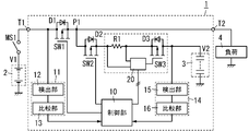
- FIG. 1 is a circuit diagram showing an overview of a backup power supply system according to Embodiment 1 of the present disclosure.
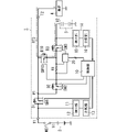
- FIG. 2 is a schematic circuit diagram of the same backup power supply system.
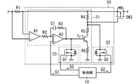
- FIG. 3 is a schematic circuit diagram of a drive circuit included in the backup power supply system;
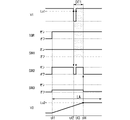
- FIG. 4 is a waveform diagram for explaining the operation of the backup power supply system of the same.
- FIG. 5 is a waveform diagram for explaining the operation of the backup power supply system of the same.
- FIG. 6 is a waveform diagram for explaining the operation of the backup power supply system of the same.
- FIG. 7 is a waveform diagram for explaining the operation of the backup power supply system of the same.
- FIG. 8 is a waveform diagram for explaining the operation of the backup power supply system;
- FIG. 1 is a circuit diagram showing an overview of a backup power supply system according to Embodiment 1 of the present disclosure.
- FIG. 2 is a schematic circuit diagram of the same backup power supply system.
- FIG. 3 is a
- FIG. 9 is a waveform diagram for explaining the operation of the backup power supply system of the same.
- FIG. 10 is a schematic explanatory diagram of a moving body provided with the backup power supply system of the same.
- FIG. 11 is a schematic circuit diagram of a backup power supply system according to Embodiment 2 of the present disclosure.
- FIG. 12 is a schematic circuit diagram of the same backup power supply system.
- FIG. 13 is a waveform diagram for explaining the operation of the backup power supply system;
- FIG. 14 is a schematic circuit diagram of a backup power supply system according to Modification 1 of the present disclosure.
- FIG. 15 is a waveform diagram for explaining the operation of the backup power supply system;
- FIG. 16 is a waveform diagram for explaining the operation of the backup power supply system;
- FIG. 15 is a waveform diagram for explaining the operation of the backup power supply system;
- FIG. 16 is a waveform diagram for explaining the operation of the backup power supply system;
- FIG. 15 is a waveform diagram for explaining the operation
- FIG. 17 is a schematic circuit diagram of a backup power supply system according to Modification 2 of the present disclosure.
- FIG. 18 is a waveform diagram for explaining the operation of the backup power supply system;
- FIG. 19 is a schematic circuit diagram of a backup power supply system according to Modification 3 of the present disclosure.
- FIG. 20 is a schematic circuit diagram of the backup power supply system of the same.
- FIG. 21 is a flowchart for explaining the operation of the backup power supply system;
- FIG. 22 is a flowchart for explaining another operation of the backup power supply system;
- FIG. 23 is a schematic circuit diagram of a backup power supply system according to Modification 4 of the present disclosure.
- the backup power supply system 1 of this embodiment includes a first connection terminal T1, a second connection terminal T2, a first field effect transistor SW1, a second field effect transistor SW2, and a second 3 field effect transistors SW3 and a control unit 10.
- FIG. 1 the backup power supply system 1 of this embodiment includes a first connection terminal T1, a second connection terminal T2, a first field effect transistor SW1, a second field effect transistor SW2, and a second 3 field effect transistors SW3 and a control unit 10.
- the main power supply 2 is connected to the first connection terminal T1.
- a load 4 is connected to the second connection terminal T2.
- the first field effect transistor SW1 is connected between the first connection terminal T1 and the second connection terminal T2.
- a series circuit of the second field effect transistor SW2 and the third field effect transistor SW3 is connected between the connection point P1 of the first field effect transistor SW1 and the second connection terminal T2 and the storage device 3 .
- the body diode D2 provided in the second field effect transistor SW2 is connected in the direction in which current flows from the connection point P1 to the storage device 3, and the body diode D3 provided in the third field effect transistor SW3 is connected from the connection point P1 to the storage device 3. It is connected in the direction in which the current flows through P1.
- the control unit 10 turns on the first field effect transistor SW1 and controls the third field effect transistor SW1 to control the charging current flowing through the storage device 3.
- Charging path RT1 is a path through which current flows from main power supply 2 to storage device 3 through first field effect transistor SW1, second field effect transistor SW2, and third field effect transistor SW3.
- the control unit 10 turns off the first field effect transistor SW1 and turns on the second field effect transistor SW2 and the third field effect transistor SW3. power is supplied from the storage device 3 to the load 4 by .
- the path through which the discharge current from power storage device 3 flows to load 4 may include backup path RT2.
- Backup route RT2 is a route through which current flows from power storage device 3 to load 4 through third field effect transistor SW3 and second field effect transistor SW2.
- the backup power supply system 1 of this embodiment is used to supply power from the power storage device 3 to the load 4 in a failure state.
- a failure state in which the main power supply 2 fails is a state in which power supply from the main power supply 2 to the load 4 is stopped due to failure, deterioration, disconnection, or the like of the main power supply 2 .
- a non-failure state in which the main power supply 2 does not fail is a state in which power is supplied from the main power supply 2 to the load 4 and the load 4 can operate with the power supplied from the main power supply 2 .
- the control unit 10 turning on the first to third field effect transistors SW1 to SW3 means operating the first to third field effect transistors SW1 to SW3 in the saturation region.
- control unit 10 controls the first to third field effect transistors SW1 to SW3 to be off means that the first to third field effect transistors SW1 to SW3 are operated in the blocking region. Even when the first to third field effect transistors SW1 to SW3 are controlled to be in the blocking region, the first to third field effect transistors SW1 to SW3 are provided with the body diodes D1 to D3. A forward current can flow through the diodes D1 to D3.
- control unit 10 operates the third field effect transistor SW3 in the active region in order to control the charging current flowing through the electricity storage device 3. For example, the control unit 10 executes current control until the charging voltage of the power storage device 3 reaches a predetermined target value (target voltage value). In addition, for example, after the charging voltage of the electricity storage device 3 reaches the target value, the control unit 10 performs constant voltage control so that the voltage does not drop due to the discharge due to the internal resistance component of the cell, thereby keeping the charging voltage constant. control (eg, trickle charge) to maintain In order to perform current control or constant voltage control, the control unit 10 operates the third field effect transistor SW3 in a saturation region or an active region (linear region) to control the magnitude of the current flowing through the third field effect transistor SW3. to control
- the charging path RT1 and the backup path RT2 share the second field effect transistor SW2 and the third field effect transistor SW3. can reduce the number of Therefore, there is an advantage that the mounting space for mounting the field effect transistor on the circuit board can be reduced and the size of the circuit board can be reduced.
- the charging path RT1 is a path through which current flows from the main power supply 2 to the storage device 3 through the first field effect transistor SW1, the second field effect transistor SW2, and the third field effect transistor SW3. If the first field effect transistor SW1 and the second field effect transistor SW2 are turned on, no voltage drop occurs due to the forward voltage of the diode. In addition, since the control unit 10 operates the third field effect transistor SW3 in the active region, the ON resistance of the third field effect transistor SW3 is small, and the voltage drop generated in the third field effect transistor SW3 is in the order of the diode. smaller than the directional voltage. Therefore, when the power storage device 3 is charged via the charging path RT1, a voltage drop due to the forward voltage of the diode does not occur.
- the backup path RT2 is a path through which current flows from the power storage device 3 to the load 4 through the third field effect transistor SW3 and the second field effect transistor SW2. If the third field effect transistor SW3 and the second field effect transistor SW2 are turned on, no voltage drop occurs due to the forward voltage of the diode, so that the voltage drop to the load 4 can be suppressed.
- the backup power supply system 1 is installed in a moving object such as a vehicle 9 (see FIG. 10). That is, the mobile includes a backup power supply system 1 and a mobile main body 91 (for example, the vehicle body of the vehicle 9). A mobile main body 91 is equipped with a backup power supply system 1 , a main power supply 2 , and a load 4 .
- a backup power supply system 1 supplies electric power from a power storage device 3 to a load 4 (for example, an electric brake system, etc.) when a main power supply 2 for a vehicle 9 (for example, a battery of the vehicle 9) fails. As a result, even if the main power supply 2 fails, the load 4 can continue to operate by power supply from the power storage device 3 .
- FIG. 10 is a schematic diagram of a vehicle 9 equipped with the backup power supply system 1, and the positions of the backup power supply system 1, the main power supply 2, and the load 4 on the vehicle body of the vehicle 9 are not limited to those shown in FIG. , can be changed as appropriate.
- the backup power supply system 1 is mounted on the vehicle 9
- the mobile body is not limited to the vehicle 9, and may be an airplane, a ship, a train, or the like.
- the backup power supply system 1 is not limited to being mounted on a moving object, and may be installed and used in a facility or the like.
- Embodiment 1 The backup power supply system 1 according to the first embodiment will be described in detail below with reference to FIGS. 2 to 9.
- FIG. 1 is a diagrammatic representation of the backup power supply system 1 according to the first embodiment.
- FIG. 2 is a specific circuit diagram of the backup power supply system 1 (see FIG. 1) described above.
- the backup power supply system 1 includes a first connection terminal T1, a second connection terminal T2, first to third field effect transistors SW1 to SW3, a control section 10, and an electric storage device 3.
- the backup power supply system 1 further includes a current detection resistor R1, a drive circuit 20, a failure detection section 11, and a charging voltage detection section .
- the electricity storage device 3 is, for example, an electrical double layer capacitor (EDLC) capable of rapid charging and discharging.
- the power storage device 3 may be composed of two or more power storage devices (for example, electric double layer capacitors) electrically connected in parallel or in series, or a plurality of power storage devices electrically connected in parallel and in series. It may be composed of a power storage device (for example, an electric double layer capacitor). That is, the power storage device 3 may be realized by a parallel circuit or a series circuit of two or more power storage devices, or a combination thereof.
- a main power supply 2 such as a battery of the vehicle 9 is connected to the first connection terminal T1 via a main switch MS1 provided in the vehicle 9 .
- the main switch MS1 When the main switch MS1 is turned on, the power supply voltage V1 is input from the main power supply 2 to the first connection terminal T1 through the main switch MS1.
- a load 4 is connected to the second connection terminal T2.
- the load 4 is, for example, an electric brake system mounted on the vehicle 9 .
- the load 4 is not limited to the electric brake system, and may be a control system or drive system device related to ADAS (Advanced Driver-Assistance Systems).
- the first to third field effect transistors SW1 to SW3 are, for example, P-channel MOSFETs (Metal-Oxide-Semiconductor Field-Effect Transistors).
- the drain of the first field effect transistor SW1 is connected to the first connection terminal T1, and the source of the first field effect transistor SW1 is connected to the second connection terminal T2.
- the body diode D1 of the first field effect transistor SW1 is connected in a direction in which current flows from the first connection terminal T1 to the second connection terminal T2.
- the drain of the second field effect transistor SW2 is connected to the connection point P1, and the source of the second field effect transistor SW2 is connected to the source of the third field effect transistor SW3 via the current detection resistor R1.
- the drain of the third field effect transistor SW3 is connected to the positive terminal of the storage device 3 .
- a negative terminal of the storage device 3 is connected to the reference potential of the backup power supply system 1 .
- the body diode D2 of the second field effect transistor SW2 prevents current from flowing from the storage device 3 toward the connection point P1.
- the third field effect transistor SW3 is turned off, the body diode D3 of the third field effect transistor SW3 prevents current from flowing from the connection point P1 toward the storage device 3 .
- the failure detection unit 11 includes a detection unit 12 and a comparison unit 13.
- the detection unit 12 detects the voltage value of the power supply voltage V1 input to the first connection terminal T1.
- the comparison unit 13 compares the voltage value of the power supply voltage V1 detected by the detection unit 12 with a threshold to determine whether the main power supply 2 is in a failed state or not. It is detected whether it is in a non-failed state.
- the comparison unit 13 outputs the detection result of the failure state or non-failure state to the control unit 10 .
- the threshold is the lower limit of the voltage range that can be regarded as a non-failure state, and is set to a value lower than the rated voltage of the main power supply 2, for example.
- the thresholds may include a first threshold for detecting occurrence of the failure state and a second threshold for detecting that the failure state has returned to the non-failure state.
- the first threshold and the second threshold may be the same value or different values.
- the charging voltage detection unit 14 includes a detection unit 15 and a comparison unit 16.
- the detection unit 15 detects the voltage value at the connection point between the third field effect transistor SW3 and the electricity storage device 3, that is, the voltage value of the charging voltage V2, which is the voltage across the electricity storage device 3.
- the comparison unit 16 compares the voltage value of the charging voltage V2 detected by the detection unit 15 and the target voltage value, and outputs the comparison result to the control unit 10 .
- the control unit 10 controls the first to third field effect transistors SW1 to SW3.
- the backup power supply system 1 has a drive circuit 20 that drives the third field effect transistor SW3. to control.
- the drive circuit 20 includes a first drive circuit 21, a second drive circuit 22, and a third drive circuit 23, as shown in FIG.
- the first drive circuit 21 generates a third electric field effect based on the voltage across the current detection resistor R1 connected between the connection point P1 and the power storage device 3 and the current command value S1 input from the control unit 10.
- Transistor SW3 is operated in the active region.
- the first drive circuit 21 includes a current detection amplifier A1, a differential amplifier A2, resistors R2 to R6, and a capacitor C1.
- the current detection amplifier A1 amplifies the voltage across the current detection resistor R1 and outputs a voltage proportional to the magnitude of the current flowing through the third field effect transistor SW3.
- the differential amplifier A2, resistors R2 and R3, and capacitor C1 constitute a differential amplifier circuit.
- the differential amplifier circuit outputs a voltage corresponding to the difference voltage between the output voltage of the current detection amplifier A1 and the current command value S1 input from the control section 10.
- the current command value S1 is a voltage signal, and the voltage value of the current command value S1 is proportional to the target value of the current flowing through the third field effect transistor SW3.
- the output voltage of the current detection amplifier A1 is higher than the current command value S1, the output voltage of the differential amplifier circuit decreases, and if the output voltage of the current detection amplifier A1 is lower than the current command value S1, the differential The output voltage of the amplifier circuit increases.
- the output voltage of the differential amplifier circuit is input to the base of the transistor Tr1.
- the emitter of transistor Tr1 is connected to the source of third field effect transistor SW3 via resistors R5 and R4.
- the collector of transistor Tr1 is connected to the reference potential through resistor R6. Since the current flowing through the transistor Tr1 changes depending on the magnitude of the output voltage of the differential amplifier circuit, the voltage between the gate and the source of the third field effect transistor SW3 changes, and the voltage between the drain and the source of the third field effect transistor SW3 changes. The resistance between the sources changes.
- the first drive circuit 21 controls the current command value S1 input from the control unit 10 so that the current flowing through the third field effect transistor SW3 becomes a current value corresponding to the current command value S1.
- 3 field effect transistor SW3 is controlled in the active region (linear region). If the current command value S1 is a constant value, current control is performed to control the charging current to the electricity storage device 3 to a constant value.
- the second drive circuit 22 turns on the third field effect transistor SW3 based on the ON signal S2 input from the control section 10.
- the second drive circuit 22 has a field effect transistor Q2 connected between the connection point of the resistors R4 and R5 and the reference potential.
- the field effect transistor Q2 is turned on in response to an on signal S2 input from the control section 10. FIG. When the field effect transistor Q2 is turned on, a voltage exceeding the pinch-off voltage is generated between the drain and source of the third field effect transistor SW3, and the third field effect transistor SW3 operates in the saturation region, that is, is turned on.
- the third drive circuit 23 turns off the third field effect transistor SW3 based on the off signal S3 input from the control section 10.
- the third drive circuit 23 has a field effect transistor Q1 connected between the base of the transistor Tr1 and the reference potential.
- the field effect transistor Q1 is turned on in response to an off signal S3 input from the control section 10. As shown in FIG. When the field effect transistor Q1 is turned on while the field effect transistor Q2 is turned off, the transistor Tr1 is turned off.
- Transistor SW3 operates in the blocking region, ie turns off.
- the backup power supply system 1 When the main switch MS1 is turned on at time t1, the backup power supply system 1 is supplied with the power supply voltage V1 from the main power supply 2. Since the voltage value of the power supply voltage V1 exceeds the threshold value Lv1 from time t1 to time t3, the failure detection unit 11 detects that the main power supply 2 is in the non-failure state. At this time, the control unit 10 turns on the first and second field effect transistors SW1 and SW2. In the first period from time t1 to time t2, the voltage value of charging voltage V2 of power storage device 3 is equal to or lower than target voltage value Lv2.
- the third field effect transistor SW3 is controlled in the saturation region or the active region so that the voltage value of the charging voltage V2 of the electric storage device 3 is controlled to the target voltage value Lv2. That is, in the non-failure state, the control unit 10 controls the charging voltage V2 of the electricity storage device 3 to reach the target voltage value Lv2 in the first period until the charging voltage V2 of the electricity storage device 3 reaches the target voltage value Lv2. Current control is performed by controlling the third field effect transistor SW3 in the saturation region or the active region. As a result, charging current flows from the main power supply 2 to the storage device 3 via the charging path RT1, and the charging voltage V2 of the storage device 3 gradually increases.
- the control unit 10 When the charging voltage V2 of the electric storage device 3 reaches the target voltage value Lv2 at time t2, the control unit 10 turns on the first field effect transistor SW1 based on the detection result of the charging voltage detection unit 14, and the second electric field The effect transistor SW2 is controlled to be off. Further, in the second period after time t2 when the charging voltage V2 reaches the target voltage value Lv2, the control unit 10 controls the charging voltage so that the charging voltage does not decrease due to the discharge due to the internal resistance component of the cells of the electricity storage device 3. The field effect transistor SW3 is controlled in the active region, and constant voltage control is performed so that the charging voltage V2 is maintained at the target voltage value Lv2.
- the control unit 10 activates the third field effect transistor SW3 so as to maintain the charging voltage V2 of the electric storage device 3 at the target voltage value Lv2 in the second period after the first period.
- the voltage is controlled by area control.
- the drain-source resistance of the third field effect transistor SW3 is get higher
- a period LA in FIG. 4 indicates a period in which the third field effect transistor SW3 is controlled in the active region.
- the failure detection unit 11 detects the failure state of the main power supply 2 and outputs the detection result to the control unit 10. output to When a failure occurs, the control unit 10 turns on the first field effect transistor SW1 and turns off the second and third field effect transistors SW2 and SW3. Since the second field effect transistor SW2 is controlled to be off, the second field effect transistor SW2 can prevent current from flowing from the power storage device 3 to the main power supply 2 side.
- the control unit 10 turns off the first field effect transistor SW1, and turns off the second and second field effect transistors SW1. 3 field effect transistors SW2 and SW3 are turned on. As a result, power is supplied from the power storage device 3 to the load 4 via the backup path RT2. Therefore, the load 4 can operate by receiving power supply from the power storage device 3 even when a failure state occurs.
- the mask period DT1 is set to a time of, for example, several tens of microseconds to several hundred microseconds. For example, even if dust or the like adheres to the main power supply 2 and a short-circuit state occurs temporarily, if the detection of the failure state by the failure detection unit 11 does not continue for the mask period DT1 or longer, the backup power supply from the power storage device 3 is stopped. Since it is not performed, malfunction of the backup power supply system 1 can be suppressed.
- the control unit 10 When the backup power supply system 1 is used in the vehicle 9, for example, when the ignition switch is turned off, the control unit 10 turns on the second and third field effect transistors SW2 and SW3 to store electricity. It is preferable to discharge the charging voltage of the device 3 .
- the control unit 10 may lower the charging voltage of the power storage device 3 compared to when the ignition switch is on, and may lower the charging voltage of the power storage device 3 to 0V.
- the ignition switch is off, the vehicle 9 is stopped and there is no need to supply backup power to the load 4. Therefore, the life of the power storage device 3 can be extended by discharging the power storage device 3.
- the failure detection unit 11 detects that a failure state has occurred because the voltage value of the power supply voltage V1 has fallen below the threshold Lv1 at time t13.
- the control unit 10 detects a failure based on the detection result of the failure detection unit 11. Decide that the problem has been resolved.
- the control unit 10 does not perform backup power supply from the power storage device 3, and controls the operation of the first to third field effect transistors SW1 to SW3 to be in the same state as from time t12 to time t14.
- a period LA in FIG. 5 indicates a period during which the third field effect transistor SW3 is controlled in the active region.
- the operation from the time t21 when the main switch MS1 is turned on to the time t24 when the backup power supply is performed is from the time t1 to the time t4 described in "(1.2.1) Operation when failure occurs after charging is completed". Since the operation is the same as the operation up to this point, the explanation thereof is omitted.
- the failure detection unit 11 detects a failure state when the voltage value of the power supply voltage V1 falls below the first threshold value Lv11, and the voltage value of the power supply voltage V1 falls below the second threshold value Lv11. When it reaches Lv12 or higher, it is detected that the state has recovered from the failed state (that is, the state is in a non-failed state).
- the control unit 10 controls the first field effect transistor SW1 to be off, and the second and third electric fields are turned off.
- the effect transistors SW2 and SW3 are controlled to be on. As a result, power is supplied from the power storage device 3 to the load 4 via the backup path RT2.
- the control unit 10 detects the second electric field based on the detection result of the failure detection unit 11.
- the effect transistor SW2 is controlled to be on, and the third field effect transistor SW3 is controlled to be off. Note that, when a failure of the main power supply 2 occurs, the control unit 10 controls the first field effect transistor SW1 to be off even after the failure state of the main power supply 2 is resolved.
- the power supply voltage V1 is higher than the charging voltage V2, power is supplied from the main power supply 2 to the load 4 via the body diode D1 of the first field effect transistor SW1.
- power supply voltage V1 is lower than charging voltage V2, power is supplied from power storage device 3 to load 4 via backup path RT2. Since the third field effect transistor SW3 is turned off, when the power supply voltage V1 of the main power supply 2 is higher than the charging voltage V2 of the storage device 3, a large current flows into the storage device 3. It can be blocked by field effect transistor SW3.
- the first field effect transistor SW1 is controlled to be off, the possibility of current flowing from the power storage device 3 to the main power supply 2 side can be reduced.
- the power supply voltage V1 is supplied from the main power supply 2 to the backup power supply system 1. Since the voltage value of the power supply voltage V1 exceeds the threshold value Lv1 from time t31 to time t32, the failure detection unit 11 detects that the main power supply 2 is in the non-failure state. At this time, the control unit 10 turns on the first and second field effect transistors SW1 and SW2. Also, from time t31 to time t32, the voltage value of charging voltage V2 of power storage device 3 is equal to or lower than target voltage value Lv2. The third field effect transistor SW3 is controlled in the active region so that the voltage value of the charging voltage V2 of is controlled to the target voltage value Lv2. As a result, charging current flows from the main power supply 2 to the storage device 3 via the charging path RT1, and the charging voltage V2 of the storage device 3 gradually increases.
- the failure detection unit 11 detects the failure state of the main power supply 2 and outputs the detection result to the control unit 10. do.
- the control unit 10 turns on the first field effect transistor SW1 and turns off the second field effect transistor SW2.
- the second field effect transistor SW2 can prevent current from flowing from the electric storage device 3 to the main power supply 2 side.
- the control unit 10 turns off the first field effect transistor SW1, and turns off the second and third field effect transistors SW1.
- the field effect transistors SW2 and SW3 are controlled to be on.
- power is supplied from the power storage device 3 to the load 4 via the backup path RT2. Therefore, the load 4 can operate by receiving power supply from the power storage device 3 even when a failure state occurs.
- the failure detection unit 11 detects that a failure state has occurred because the voltage value of the power supply voltage V1 has fallen below the threshold value Lv1 at time t42.
- the control unit 10 detects a failure based on the detection result of the failure detection unit 11. Decide that the problem has been resolved.
- the control unit 10 does not perform backup power supply from the electricity storage device 3, controls the operation of the first to third field effect transistors SW1 to SW3 to be in the same state as from time t41 to time t42, and controls the operation of the electricity storage device 3. 3 continue charging.
- the control unit 10 turns on the first field effect transistor SW1 and turns on the second field effect transistor SW1 based on the detection result of the charging voltage detection unit 14. to turn off the field effect transistor SW2.
- the control unit 10 controls the third field effect transistor SW3 in the active region so that the charging voltage V2 of the power storage device 3 is maintained at the target voltage value Lv2.
- Trickle charge device 3 At this time, the current flowing through the third field effect transistor SW3 becomes smaller than that in the first period, so the drain-source resistance of the third field effect transistor SW3 becomes higher than that in the first period.
- a period LA in FIG. 8 indicates a period during which the third field effect transistor SW3 is controlled in the active region.
- the operation from time t51 when the main switch MS1 is turned on to time t53 when the backup power supply is performed is from time t31 to time t33 described in "(1.2.4) Operation when failure occurs during charging". Since the operation is the same as the operation up to this point, the explanation thereof is omitted.
- the failure detection unit 11 detects a failure state when the voltage value of the power supply voltage V1 falls below the first threshold value Lv11, and the voltage value of the power supply voltage V1 falls below the second threshold value. When it reaches Lv12 or higher, it is detected that the state has recovered from the failed state.
- the control unit 10 controls the first field effect transistor SW1 to be off, and the second and third electric fields are turned off.
- the effect transistors SW2 and SW3 are controlled to be on. As a result, power is supplied from the power storage device 3 to the load 4 via the backup path RT2.
- the control unit 10 detects the second electric field based on the detection result of the failure detection unit 11.
- the effect transistor SW2 is controlled to be on, and the third field effect transistor SW3 is controlled to be off. Note that, when a failure of the main power supply 2 occurs, the control unit 10 controls the first field effect transistor SW1 to be off even after the failure state of the main power supply 2 is resolved.
- the power supply voltage V1 is higher than the charging voltage V2, power is supplied from the main power supply 2 to the load 4 via the body diode D1 of the first field effect transistor SW1.
- power supply voltage V1 is lower than charging voltage V2, power is supplied from power storage device 3 to load 4 via backup path RT2. Since the third field effect transistor SW3 is turned off, when the power supply voltage V1 of the main power supply 2 is higher than the charging voltage V2 of the storage device 3, a large current flows into the storage device 3. It can be blocked by field effect transistor SW3.
- the first field effect transistor SW1 is controlled to be off, the possibility of current flowing from the power storage device 3 to the main power supply 2 side can be reduced.
- the backup power supply system 1 of the present embodiment can supply backup power from the power storage device 3 to the load 4 when the main power supply 2 fails.
- FIGS. 11 and 12 are schematic circuit diagrams of the backup power supply system 1 according to the second embodiment.
- the backup power supply system 1 of the second embodiment further includes a second power storage device 3B different from the first power storage device 3A, which is the power storage device 3 described in the first embodiment.
- the backup power supply system 1 further includes a fourth field effect transistor SW4 and a switching circuit 30 .
- the fourth field effect transistor SW4 is connected between the terminal (that is, source) of the second field effect transistor SW2 on the side of the third field effect transistor SW3 and the second power storage device 3B.
- a current detection resistor R1A is connected between the second field effect transistor SW2 and the third field effect transistor SW3, and a current detection resistor R1A is connected between the second field effect transistor SW2 and the fourth field effect transistor SW4.
- a resistor R1B is connected.
- the fourth field effect transistor SW4 is connected via the current detection resistor R1B to the connection point P2 between the second field effect transistor SW2 and the current detection resistor R1A.
- the backup power supply system 1 further includes a drive circuit 20A that drives the third field effect transistor SW3 and a drive circuit 20B that drives the fourth field effect transistor SW4.
- the control unit 10 controls the fourth field effect transistor SW4 in the active region in order to control the charging current flowing through the second power storage device 3B. Further, when power is supplied from the second power storage device 3B to the load 4 in the failure state, the control unit 10 controls the fourth field effect transistor SW4 to be ON.
- the drive circuits 20A and 20B have the same configuration and functions as the drive circuit 20 described in the first embodiment, so description thereof will be omitted.
- the backup power supply system 1 further includes a first charging voltage detection section 14A and a second charging voltage detection section 14B.
- the first charging voltage detection unit 14A includes a detection unit 15A and a comparison unit 16A, and detects a charging voltage V2, which is the terminal voltage on the positive terminal side of the first power storage device 3A.
- the second charging voltage detection unit 14B includes a detection unit 15B and a comparison unit 16B, and detects a charging voltage V3, which is the terminal voltage on the positive electrode side of the second power storage device 3B.
- the first charging voltage detection unit 14A and the second charging voltage detection unit 14B have the same configuration and function as the charging voltage detection unit 14 described in the first embodiment, so description thereof will be omitted.
- the switching circuit 30 switches to the first state or the second state according to the switching signal from the control section 10 .
- a first state between the second field effect transistor SW2 and the reference potential, a series circuit of the third field effect transistor SW3 and the first power storage device 3A, a fourth field effect transistor SW4 and the second power storage device 3B series circuit is connected in parallel.
- the second state between the second field effect transistor SW2 and the reference potential, the first power storage device 3A and the second power storage device 3A are connected via a parallel circuit of the third field effect transistor SW3 and the fourth field effect transistor SW4.
- the device 3B is connected in series.
- a current detection resistor R1A is connected between the connection point P2 and the third field effect transistor SW3, and a current detection resistor R1A is connected between the connection point P2 and the fourth field effect transistor SW4.
- R1B is connected. Therefore, in the first state, a series circuit of the current detection resistor R1A, the third field effect transistor SW3, and the first storage device 3A, and the current detection resistor R1B are placed between the second field effect transistor SW2 and the reference potential. and a series circuit of the fourth field effect transistor SW4 and the second storage device 3B are connected in parallel.
- a series circuit of a current detection resistor R1A and a third field effect transistor SW3, a current detection resistor R1B and a fourth field effect transistor are placed between the second field effect transistor SW2 and the reference potential.
- the first power storage device 3A and the second power storage device 3B are connected in series via a parallel circuit in which the series circuit of SW4 is connected in parallel.
- the switching circuit 30 includes four switches SW5 to SW8.
- the switches SW5 to SW8 are composed of MOSFETs, for example.
- the switch SW5 is connected between the drain of the third field effect transistor SW3 and the drain of the fourth field effect transistor SW4.
- the switch SW6 is connected between the drain of the third field effect transistor SW3 and the positive terminal of the first storage device 3A.
- the switch SW7 is connected between the positive terminal of the first electric storage device 3A and the negative terminal of the second electric storage device 3B.
- the switch SW8 is connected between the negative terminal of the second power storage device 3B and the reference potential.
- the switching circuit 30 realizes the first state by turning off the switches SW5 and SW7 and turning on the switches SW6 and SW8 according to the switching signal from the control unit 10 .
- the switching circuit 30 realizes the second state by turning on the switches SW5 and SW7 and turning off the switches SW6 and SW8 according to the switching signal from the control unit 10 .
- the backup power supply system 1 When the main switch MS1 is turned on at time t61, the backup power supply system 1 is supplied with the power supply voltage V1 from the main power supply 2.
- the failure detection unit 11 detects that the main power supply 2 is in the non-failure state.
- the control unit 10 turns on the first and second field effect transistors SW1 and SW2. Further, the control unit 10 turns on the switches SW5 and SW7, turns off the switches SW6 and SW8, and switches the switching circuit 30 to the second state. Further, the control unit 10 operates the third and fourth field effect transistors SW3 and SW4 in the active region in order to control the charging currents flowing through the first power storage device 3A and the second power storage device 3B.
- a path RT11 from the main power supply 2 through a parallel circuit of the first field effect transistor SW1, the second field effect transistor SW2, the third and fourth field effect transistors SW3 and SW4, and the second power storage device 3B and the A charging current flows through the series circuit with the first power storage device 3A.
- a large charging current flows through the first power storage device 3A and the second power storage device 3B, and the charging time of the first power storage device 3A and the second power storage device 3B is shortened.
- the third field effect transistor SW3 and the fourth field effect transistor SW4 for controlling the charging current are connected in parallel, the impedance of the circuit can be reduced, and the loss can be reduced.
- the charging voltage V3 detected by the second charging voltage detection unit 14B is the voltage of the first power storage device 3A. It is a voltage value obtained by adding the charging voltage V2 and the charging voltage of the second power storage device 3B.
- the control section 10 turns off the switches SW5 and SW7 and turns on the switches SW6 and SW8. and switches the switching circuit 30 to the first state.
- the switching circuit 30 switches to the first state according to the switching signal.
- a charging current flows from the main power supply 2 through the first, second, and third field effect transistors SW1, SW2, and SW3 to the first electric storage device 3A, and the first, second, and A charging current flows through the fourth field effect transistors SW1, SW2, SW4 to the second storage device 3B. That is, a charging current flows from the main power supply 2 to the first power storage device 3A and the second power storage device 3B via the path RT12 (see FIG. 11), and the first power storage device 3A and the second power storage device 3B each reach the target voltage value Lv2.
- control unit 10 controls the third and fourth field effect transistors SW3 so that the charging voltage of the electric storage device 3 becomes a predetermined target voltage value Lv2 during the period from time t61 to time t63 (first period). , SW4 are controlled in the active region to perform current control.
- the control unit 10 controls the first charging voltage detection unit 14A and the second charging voltage detection unit Based on the detection result of 14B, the first field effect transistor SW1 is controlled to be ON and the second field effect transistor SW2 is controlled to be OFF.
- the control unit 10 controls the third and fourth electric fields so that the charging voltage V2 of the first power storage device 3A and the second power storage device 3B is maintained at the target voltage value Lv2. Voltage control is performed by controlling the effect transistors SW3 and SW4 in their active regions, and the electric storage device 3 is trickle charged.
- a period LA in FIG. 13 indicates a period during which the third and fourth field effect transistors SW3 and SW4 are controlled in the active region.
- the failure detection unit 11 detects the failure state of the main power supply 2 and outputs the detection result to the control unit 10. output to
- the control unit 10 When the failure state continues for the mask period DT1 from time t64 when the failure of the main power supply 2 is detected, the control unit 10 turns off the first field effect transistor SW1 at time t65, and the second and third electric fields are restored.
- the effect transistors SW2 and SW3 are controlled to be on. Further, the control unit 10 turns on the switches SW5 and SW7, turns off the switches SW6 and SW8, and switches the switching circuit 30 to the second state. That is, when power is supplied to the load 4 from the first power storage device 3A and the second power storage device 3B in the failed state, the switching circuit 30 switches to the second state according to the switching signal.
- a backup path RT13 is formed from the first power storage device 3A and the second power storage device 3B through the parallel circuit of the third field effect transistor SW3 and the fourth field effect transistor SW4, and the second field effect transistor SW2. (See FIG. 12) to supply power to the load 4 .
- the first power storage device 3A and the second power storage device 3B are connected in series, a voltage higher than the charging voltage of each of the first power storage device 3A and the second power storage device 3B is supplied to the load 4. be able to.
- the control unit 10 when charging the first power storage device 3A and the second power storage device 3B in the non-failure state, the control unit 10 first outputs a switching signal for switching to the second state to the switching circuit 30. , charges the first power storage device 3A and the second power storage device 3B in the second state (period t61 to t62). Then, when the charging voltages of the first power storage device 3A and the second power storage device 3B connected in series reach a predetermined switching voltage value Lv3, the control unit 10 sends a switching signal for switching to the first state to the switching circuit 30. The first power storage device 3A and the second power storage device 3B are each charged in the first state.
- the first power storage device 3A and the second power storage device 3B are first charged in the second state in which they are connected in series, so the first power storage device 3A and the second power storage device 3B can be charged in a short time. Further, a series circuit of the current detection resistor R1A and the third field effect transistor SW3 and a series circuit of the current detection resistor R1B and the fourth field effect transistor SW4 are connected in parallel to form the first power storage device. Since 3A and the second power storage device 3B are charged, loss in the charging path can be reduced.
- the first power storage device 3A and the second power storage device 3B connected in series reach the switching voltage value Lv3
- the first power storage device 3A and the second power storage device 3B are charged in the first state.
- the first power storage device 3A and the second power storage device 3B can be charged up to the target voltage value Lv2.
- the control unit 10 when charging the first power storage device 3A and the second power storage device 3B in the non-failure state, the control unit 10 does not provide a period in which the second state is set, and maintains the first state in the first state. You may charge the electrical storage device 3A and the 2nd electrical storage device 3B. That is, the control unit 10 switches to the first state by the switching circuit 30 when charging the first power storage device 3A and the second power storage device 3B in the non-failed state, and switches to the second state by the switching circuit 30 when charging the backup power supply. can be controlled as follows.
- a control method for the backup power supply system 1 includes a charging step and a backup power feeding step.
- the backup power supply system 1 includes a first connection terminal T1, a second connection terminal T2, and first to third field effect transistors SW1 to SW3.
- a main power supply 2 is connected to the first connection terminal T1, and a load 4 is connected to the second connection terminal T2.
- the first field effect transistor SW1 is connected between the first connection terminal T1 and the second connection terminal T2.
- a series circuit of the second field effect transistor SW2 and the third field effect transistor SW3 is connected between the connection point P1 of the first field effect transistor SW1 and the second connection terminal T2 and the storage device 3 .
- a body diode D2 included in the second field effect transistor SW2 is connected in a direction in which current flows from the connection point P1 to the electric storage device 3 .
- a body diode D3 included in the third field effect transistor SW3 is connected in a direction in which current flows from the power storage device 3 to the connection point P1.
- the first field effect transistor SW1 is turned on and the third field effect transistor SW1 is turned on to control the charging current flowing to the storage device 3 in a non-failure state where the main power supply 2 is not failed.
- SW3 is controlled in the active region.
- the electric storage device 3 is charged from the main power supply 2 through the charging path RT1 passing through the first field effect transistor SW1, the second field effect transistor SW2 and the third field effect transistor SW3.
- the first field effect transistor SW1 is turned off, and the second field effect transistor SW2 and the third field effect transistor SW3 are controlled to be on in a failed state in which the main power supply 2 is failed.
- the path for supplying power from the storage device 3 to the load 4 may include a backup path RT2 passing from the storage device 3 through the third field effect transistor SW3 and the second field effect transistor SW2.
- a (computer) program according to one aspect is a program for causing a computer system to execute a control method of the backup power supply system 1 .
- the backup power supply system 1 in the present disclosure includes a computer system to realize the control unit 10, for example.
- a computer system is mainly composed of a processor and a memory as hardware.
- the functions of the backup power supply system 1 in the present disclosure are realized by the processor executing a program recorded in the memory of the computer system.
- the program may be recorded in advance in the memory of the computer system, may be provided through an electric communication line, or may be recorded in a non-temporary recording medium such as a computer system-readable memory card, optical disk, or hard disk drive. may be provided.
- a processor in a computer system consists of one or more electronic circuits, including semiconductor integrated circuits (ICs) or large scale integrated circuits (LSIs).
- Integrated circuits such as ICs or LSIs are called differently depending on the degree of integration, and include integrated circuits called system LSI, VLSI (Very Large Scale Integration), or ULSI (Ultra Large Scale Integration).
- FPGAs Field-Programmable Gate Arrays
- a plurality of electronic circuits may be integrated into one chip, or may be distributed over a plurality of chips.
- a plurality of chips may be integrated in one device, or may be distributed in a plurality of devices.
- a computer system includes a microcontroller having one or more processors and one or more memories. Accordingly, the microcontroller also consists of one or more electronic circuits including semiconductor integrated circuits or large scale integrated circuits.
- control unit 10 is not limited to being implemented by a computer system, and may be implemented by an analog circuit.
- the backup power system 1 it is not an essential configuration of the backup power system 1 that a plurality of functions in the backup power system 1 are integrated in one housing, and the components of the backup power system 1 are distributed over a plurality of housings. may be provided. Furthermore, at least part of the functions of the backup power supply system 1, for example, part of the functions of the control unit 10, may be realized by the cloud (cloud computing) or the like. Further, when the backup power supply system 1 is mounted on the vehicle 9 , some functions of the control unit 10 may be realized by an ECU (Electronic Control Unit) of the vehicle 9 .
- ECU Electronic Control Unit
- the backup power supply system 1 of Modification 1 differs from the backup power supply system 1 of Embodiment 1 in that it further includes a bypass field effect transistor SW10.
- symbol is attached
- a first end (drain) of the bypass field effect transistor SW10 is connected to the second connection terminal T2, and a second end (source) of the bypass field effect transistor SW10 is connected to the second electric field in the third field effect transistor SW3. It is connected to the terminal (source) on the side of the effect transistor SW2. That is, the body diode D10 of the bypass field effect transistor SW10 is connected in the direction in which the current flows from the second connection terminal T2 to the storage device 3 .
- the control unit 10 When the failure state continues for the mask period DT1 from time t71 when the failure of the main power supply 2 is detected (time t72), the control unit 10 turns off the first field effect transistor SW1, and turns off the second and third field effect transistors SW1.
- the field effect transistors SW2 and SW3 are controlled to be on.
- the control unit 10 turns on the bypass field effect transistor SW10.
- the load 4 can operate by receiving power supply from the power storage device 3 even when a failure state occurs.
- the backup path RT3 does not include the current detection resistor R1, the loss due to the current detection resistor R1 can be reduced.
- the control unit 10 turns on the first and second field effect transistors SW1 and SW2, and controls the third field effect transistor SW3 in the active region, thereby suppressing malfunction of the backup power supply system 1. can be done.
- the backup power supply system 1 of Modification 2 differs from the backup power supply system 1 of Embodiment 2 in that it further includes a first bypass field effect transistor SW11 and a second bypass field effect transistor SW12.
- symbol is attached
- the first bypass field effect transistor SW11 has a first terminal (drain) connected to the second connection terminal T2, and a terminal (source) of the third field effect transistor SW3 on the side of the second field effect transistor SW2. Two ends (sources) are connected.
- the second bypass field effect transistor SW12 has a first terminal (drain) connected to the second connection terminal T2, and a terminal (source) of the fourth field effect transistor SW4 on the side of the second field effect transistor SW2. Two ends (sources) are connected. That is, the body diode D11 of the first bypass field effect transistor SW11 is connected in the direction in which the current flows from the second connection terminal T2 to the first power storage device 3A, and the body diode D12 of the second bypass field effect transistor SW12 is connected. are connected in a direction in which current flows from the second connection terminal T2 to the second electric storage device 3B.
- the operation of the backup power supply system 1 of Modification 2 will be described based on FIG.
- the operation from time t91 to time t95 until the start of backup power supply is the same as the operation from time t61 to time t65 described in "(2.2) Operation", so description thereof will be omitted.
- the control unit 10 controls the first and second bypass field effect transistors SW11 and SW12 to be off from time t91 to time t95.
- the control unit 10 When the failure state continues for the mask period DT1 from time t94 when the failure of the main power supply 2 is detected, the control unit 10 turns off the first field effect transistor SW1 at time t95, and the second and third electric fields are restored.
- the effect transistors SW2 and SW3 are controlled to be on. Further, the control unit 10 turns on the switches SW5 and SW7, turns off the switches SW6 and SW8, and switches the switching circuit 30 to the second state. Then, when power is supplied to the load 4 from the first power storage device 3A and the second power storage device 3B in the failure state, the control unit 10 enables the first bypass field effect transistor SW11 and the second bypass field effect transistor SW12. control on.
- the series circuit of the third field effect transistor SW3 and the first bypass field effect transistor SW11, the fourth field effect transistor SW4 and the second Power is supplied to the load 4 via a backup path RT14 (see FIG. 17) passing through a parallel circuit in which a series circuit with a bypass field effect transistor SW12 is connected in parallel. Therefore, the load 4 can operate by receiving power supply from the first power storage device 3A and the second power storage device 3B even when a failure state occurs. Moreover, since the backup path RT14 does not include the current detection resistors R1A and R1B, the loss due to the current detection resistors R1A and R1B can be reduced.
- the first bypass field effect transistor SW11 is not essential, and can be omitted as appropriate.
- power may be supplied to the load 4 from the first power storage device 3A and the second power storage device 3B connected in series via the second bypass field effect transistor SW12.
- the backup power supply system 1 of Modification 3 differs from Modification 1 above in that, when power is supplied from the power storage device 3 to the load 4 in a failed state, the power supply path is changed according to the type of the load 4 .
- symbol is attached
- the control unit 10 selects the first route RT4 (see FIG. 19) and the first route RT4 (see FIG. 19) and Switch to any of the second routes RT5 (see FIG. 20).
- a first path RT4 is a path for supplying power from the storage device 3 to the load 4 via the third field effect transistor SW3 and the second field effect transistor SW2.
- a second path RT5 is a path for supplying power from the power storage device 3 to the load 4 via the bypass field effect transistor SW10.
- the first path RT4 is a path for supplying power from the power storage device 3 to the load 4 via the third field effect transistor SW3, the current detection resistor R1, and the second field effect transistor SW2.
- a second route RT5 is a route for supplying power from the storage device 3 to the load 4 via the third field effect transistor SW3 and the bypass field effect transistor SW10.
- the load 4 to which the backup power supply system 1 performs backup power supply includes at least one of a capacitive load and a resistive load.
- the capacitive load includes, for example, a DC-DC converter having a capacitive component such as a smoothing electrolytic capacitor in the input stage.
- resistive loads include motors having windings that are resistance components.
- the control unit 10 acquires load information about the load 4 to which backup power supply is to be performed, for example, from the ECU 5 of the vehicle 9 .
- the control unit 10 periodically communicates with the ECU 5 and acquires load information from the ECU 5 .
- the load information is information indicating whether the load 4 is a capacitive load or a resistive load, and may be information about the name or type of the load 4, or whether the load 4 is a capacitive load or a resistive load. It may be the type information itself indicating whether or not there is. If the load information is information about the name (for example, motor, DC-DC converter, etc.) or type of the load 4, the control unit 10 determines whether the load 4 is a capacitive load or a resistive load based on the load information. should be judged.
- the control unit 10 preferably sets the first route RT4 as the route for supplying power from the power storage device 3 to the load 4 . Since the first path RT4 includes the current detection resistor R1, the first path RT4 has a higher path resistance than the second path RT5. Therefore, by supplying power from the power storage device 3 to the load 4, which is a capacitive load, through the first path RT4, it is possible to suppress the inrush current from flowing into the load 4.
- the control unit 10 preferably sets the second route RT5 as the route for supplying power from the power storage device 3 to the load 4 .
- the second path RT5 is a path for supplying power from the power storage device 3 to the load 4 via the third field effect transistor SW3 and the bypass field effect transistor SW10. is small, the loss due to path resistance can be reduced.
- the control unit 10 switches the power supply route to the first route RT4 from the occurrence of the failure state to the satisfaction of the switching condition, and switches the power supply route to the first route RT4 when the switching condition is satisfied. to the second route RT5.
- the control unit 10 sets the first path RT4 as the path for supplying power from the power storage device 3 to the load 4 from the occurrence of the failure state to the satisfaction of the switching condition, so that a large inrush current is generated in the load 4. suppress the flow. Then, when the switching condition is established, the control unit 10 sets the second route RT5 as the route for supplying power from the power storage device 3 to the load 4, thereby reducing loss due to route resistance.
- the above switching conditions are the condition that a certain period of time has passed since the failure state occurred, the condition that the discharge current from the electricity storage device 3 becomes equal to or less than the threshold current, and the condition that the charging voltage V2 of the electricity storage device 3 is the threshold value. It is preferable to include at least one of the condition that the voltage is below the voltage and the condition that the charging rate of the electricity storage device 3 is below the threshold. If at least one of these conditions holds, the inrush current flowing into the load 4 will be smaller than if none of the conditions hold, so a large inrush current may flow into the circuit including the load 4. can be reduced.
- FIG. 21 shows the operation when the switching condition includes the condition that a certain period of time has elapsed since the failure state occurred and the condition that the discharge current from the electricity storage device 3 becomes equal to or less than the threshold current.
- the control unit 10 periodically communicates with the ECU 5 of the vehicle and acquires load information from the ECU 5 (step ST1).
- the load information includes, for example, information on the name of the load 4 that performs backup power supply.
- Information indicating whether the load 4 is a capacitive load or a resistive load is stored in the memory of the control unit 10 in association with the name of the load 4 . Therefore, based on the load information (the name of the load 4) acquired from the ECU 5, the control unit 10 determines whether the load 4 to which backup power supply is to be performed is a capacitive load or a resistive load.
- step ST3 the control unit 10 determines whether or not the load 4 to which backup power supply is to be performed is a capacitive load.
- step ST3 If the load 4 targeted for backup power supply is a capacitive load (step ST3: Yes), the control unit 10 turns off the first field effect transistor SW1, turns off the second and third field effect transistors SW1 after the mask period DT1 has passed. The field effect transistors SW2 and SW3 are turned on, and the bypass field effect transistor SW10 is turned off. At this time, power is supplied from the storage device 3 to the load 4 via the first path RT4 (step ST4). Since the first path RT4 includes the current detection resistor R1, the inrush current flowing into the load 4 can be suppressed, and the circuit including the load 4 can be protected. Since power is supplied from the power storage device 3 to the load 4 via the first path RT4, the load 4 can continue to operate even in a failed state.
- step ST5 determines that the switching condition is satisfied (step ST5: Yes)
- the controller 10 turns on the bypass field effect transistor SW10.
- step ST6 since power is supplied from the storage device 3 to the load 4 via the second path RT5 (step ST6), loss due to path resistance can be reduced.
- step ST3 when it is determined that the load 4 to be subjected to backup power supply is a resistive load (step ST3: No), the control unit 10 controls the first electric field after the mask period DT1 has elapsed.
- the effect transistor SW1 is turned off, the second and third field effect transistors SW2 and SW3 are turned on, and the bypass field effect transistor SW10 is turned on.
- power is supplied from the storage device 3 to the load 4 via the second path RT5 (step ST6).
- the control unit 10 supplies power to the load 4 via the second path RT5 from the start of the backup power supply, thereby reducing the loss due to the path resistance of the power supply path and making it possible to supply a large amount of power to the load 4. .
- the control unit 10 determines whether or not a stop condition for stopping backup power supply is satisfied (step ST7).
- the stop condition may include, for example, the condition that the charging voltage V2 of the power storage device 3 becomes equal to or lower than a predetermined overdischarge level. If the voltage value of the charging voltage V2 detected by the charging voltage detection unit 14 is higher than the overdischarge level, the control unit 10 determines that the stop condition is not satisfied (step ST7: No), and shifts to the second route RT5.
- step ST7 Yes
- step ST8 the control unit 10 determines that the stop condition is met
- step ST7: Yes the control unit 10 determines that the stop condition is met
- step ST7: Yes the control unit 10 determines that the stop condition is met
- the field effect transistors SW1, SW2, and SW3 are turned off, and the bypass field effect transistor SW10 is turned off to stop the discharge from the storage device 3 (step ST8) and stop the power supply from the storage device 3 to the load 4.
- the control method of the backup power supply system 1 of Modification 3 further includes a switching step.
- the switching step selects either the first route RT4 or the second route RT5 as the power supply route to the load 4 in the failure state based on the load information indicating whether the load 4 is a capacitive load or a resistive load.
- switch to A first path RT4 is a path for supplying power from the storage device 3 to the load 4 via the third field effect transistor SW3 and the second field effect transistor SW2.
- a second path RT5 is a path for supplying power from the power storage device 3 to the load 4 via the bypass field effect transistor SW10.
- the bypass field effect transistor SW10 has a first end connected to the second connection terminal T2, and a second end connected to a terminal of the third field effect transistor SW3 on the side of the second field effect transistor SW2.
- control unit 10 may store, in a memory included in the control unit 10, power supply target information indicating whether the load 4 to which the backup power supply was performed last time is a capacitive load or a resistive load. . If the load information cannot be acquired from the ECU 5 due to a communication failure or the like in step ST1, the control unit 10 determines whether the load 4 to which backup power supply is to be performed is a capacitive load or a resistive load based on the power supply target information read from the memory. You may judge whether it is a load.
- the above switching conditions can be changed as appropriate. and a condition that it becomes equal to or less than Sth1 (hereinafter referred to as a second condition).
- a condition that it becomes equal to or less than Sth1 hereinafter referred to as a second condition.
- the operation when the switching condition includes the first condition and the second condition will be described with reference to FIG.
- the control unit 10 periodically communicates with the ECU 5 of the vehicle and acquires load information from the ECU 5 (step ST11).
- the load information includes, for example, information about the name of the load 4 to which backup power supply is to be performed. Determine whether it is a load or a resistive load.
- step ST12 determines whether or not the load 4 to which backup power supply is to be performed is a capacitive load (step ST13).
- step ST13 If the load 4 targeted for backup power supply is a capacitive load (step ST13: Yes), the control unit 10 determines whether or not the first condition and the second condition are satisfied after the mask period DT1 has elapsed. do. If at least one of the first condition and the second condition is not satisfied, the control unit 10 turns off the first field effect transistor SW1, turns on the second and third field effect transistors SW2 and SW3, and turns on the bypass field effect transistor. Turn off transistor SW10.
- the control unit 10 controls the electricity storage device 3 to Power is supplied to the load 4 via the 1-path RT4 (step ST15). Since the first path RT4 includes the current detection resistor R1, the inrush current flowing into the load 4 can be suppressed, and the circuit including the load 4 can be protected.
- the control unit 10 monitors the charging voltage V2 and the charging rate SOC of the electricity storage device 3, and if at least one of the first condition and the second condition is not satisfied (step ST16: No), the electricity storage device 3 changes to the first charge. Power is supplied to the load 4 via the route RT4 (step ST15). That is, when the charging voltage V2 of the electricity storage device 3 is equal to or higher than the threshold voltage Vth1, or the charging rate SOC of the electricity storage device 3 is equal to or higher than the threshold Sth1, power is supplied from the electricity storage device 3 to the load 4 via the first route RT4. supply.
- step ST16 when both the first condition and the second condition are satisfied, that is, when the charging voltage V2 of the electric storage device 3 becomes less than the threshold voltage Vth1 and the state of charge SOC of the electric storage device 3 becomes less than the threshold Sth1 (step ST16: Yes), the controller 10 turns on the bypass field effect transistor SW10. At this time, power is supplied from the storage device 3 to the load 4 via the second path RT5 (step ST17).
- the second path RT5 is a path for supplying power from the power storage device 3 to the load 4 via the third field effect transistor SW3 and the bypass field effect transistor SW10. is small, the loss due to path resistance can be reduced.
- step ST13 when it is determined that the load 4 to which backup power supply is performed is a resistive load (step ST13: No), the control unit 10 turns off the first field effect transistor SW1, and turns off the first field effect transistor SW1. The second and third field effect transistors SW2 and SW3 are turned on, and the bypass field effect transistor SW10 is turned on. At this time, power is supplied from the storage device 3 to the load 4 via the second path RT5 (step ST17).
- step ST14 if both the first condition and the second condition are satisfied, that is, the charging voltage V2 of the electricity storage device 3 becomes less than the threshold voltage Vth1, and the charging rate SOC of the electricity storage device 3 reaches the threshold value Sth1.
- the first field effect transistor SW1 is turned off, the second and third field effect transistors SW2 and SW3 are turned on, and the bypass field effect transistor SW10 is turned on.
- the charging voltage V2 is less than the threshold voltage Vth1 and the charging rate SOC of the power storage device 3 is less than the threshold Sth1, it is unlikely that a large inrush current will flow into the load 4.
- a second route RT5 is set as a route for supplying power from 3 to load 4 . At this time, power is supplied from the storage device 3 to the load 4 via the second path RT5 (step ST17), so that the loss due to the path resistance can be reduced while suppressing the inrush current flowing into the load 4.
- the control unit 10 determines whether or not the stop condition for stopping the backup power supply is satisfied (step ST18).
- the stop conditions may include, for example, a condition that the charging voltage V2 of the electricity storage device 3 is equal to or less than a predetermined reference voltage, and a condition that the state of charge SOC of the electricity storage device 3 is equal to or less than a predetermined reference ratio.
- the reference voltage is set to a value lower than the threshold voltage Vth1
- the reference ratio is set to a value lower than the threshold voltage Sth1.
- the control unit 10 determines that the stop condition is met (step ST18: Yes), and the first to third electric fields The effect transistors SW1, SW2 and SW3 are turned off, and the bypass field effect transistor SW10 is turned off to stop the discharge from the electric storage device 3 (step ST19) and stop the power supply from the electric storage device 3 to the load 4.
- the stop conditions include the condition that the charging voltage V2 of the electricity storage device 3 becomes equal to or lower than the reference voltage and the condition that the state of charge SOC of the electricity storage device 3 becomes equal to or lower than the reference ratio. Only one condition may be used.
- the stop condition is not limited to the above conditions, and the stop condition may include a condition that the discharge current from the electricity storage device 3 is equal to or less than a predetermined reference current.
- the bypass field effect transistor SW10 may be connected between the connection point between the third field effect transistor SW3 and the electric storage device 3 and the second connection terminal T2. good.
- the second path RT5 serves as a path for supplying power from the power storage device 3 to the load 4 via the bypass field effect transistor SW10.
- the backup power supply system 1 of Modification 4 differs from Modification 2 above in that, when power is supplied from the power storage device 3 to the load 4 in a failed state, the power supply path is changed according to the type of the load 4 .
- symbol is attached
- control unit 10 supplies power to the load in a failure state based on load information indicating whether the load 4 is a capacitive load or a resistive load.
- the route is switched to either the first route RT15 or the second route RT16 (see FIG. 23).
- a first path RT15 extends from the first power storage device 3A and the second power storage device 3B connected in series via the third field effect transistor SW3, the fourth field effect transistor SW4, and the second field effect transistor SW2. This is the route through which the load 4 is supplied with power.
- a second path RT16 extends from the first power storage device 3A and the second power storage device 3B, which are connected in series, to a series circuit of a first bypass field effect transistor SW11 and a third field effect transistor SW3, and a second bypass field effect transistor SW3.
- This path supplies power to the load 4 through at least one of the series circuit of the second field effect transistor SW12 and the fourth field effect transistor SW4.
- the control unit 10 switches the power supply route to the first route RT15 from the occurrence of the failure state until the switching condition is satisfied, and switches the power supply route to the first route RT15 when the switching condition is satisfied. to the second route RT16.
- the control unit 10 sets the first path RT15 as the path for supplying power from the power storage device 3 to the load 4 from the occurrence of the failure state to the satisfaction of the switching condition, so that a large inrush current is generated in the load 4. suppress the flow. Then, when the switching condition is established, the control unit 10 sets the second route RT16 as the route for supplying power from the power storage device 3 to the load 4, thereby reducing loss due to route resistance.
- the above switching conditions include the condition that a certain period of time has passed since the failure state occurred, the condition that the discharge current from the first power storage device 3A and the second power storage device 3B becomes equal to or less than the threshold current, and the Of the condition that the voltage obtained by adding the charging voltages of the first power storage device 3A and the second power storage device 3B is equal to or less than the threshold voltage and the condition that the charging rate of the first power storage device 3A and the second power storage device 3B is equal to or less than the threshold It preferably contains at least one.
- the voltage obtained by adding the charging voltages of the first power storage device 3A and the second power storage device 3B is the charging voltage V3 when the first power storage device 3A and the second power storage device 3B are connected in series.
- the charging rate of the first power storage device 3A and the second power storage device 3B is the charge rate of the first power storage device 3A and the second power storage device 3B with respect to the total value of the charge capacities of the first power storage device 3A and the second power storage device 3B. It is the ratio of the total value of the quantity. If at least one of these conditions is met, the inrush current flowing into the load 4 will be smaller than when none of the conditions are met. can be reduced.
- Modified Example 4 it is not essential to provide both the first bypass field effect transistor SW11 and the second bypass field effect transistor SW12, and the first bypass field effect transistor SW11 and the second bypass field effect transistor SW11 are provided. Alternatively, only one of the field effect transistors SW12 may be provided. In this case, from the first power storage device 3A and the second power storage device 3B that are connected in series, the series circuit of the first bypass field effect transistor SW11 and the third field effect transistor SW3 and the second bypass electric field Power may be supplied to the load 4 via either one of the series circuit of the effect transistor SW12 and the fourth field effect transistor SW4.
- the first bypass field effect transistor SW11 is connected between the terminal of the third field effect transistor SW3 on the side of the first power storage device 3A and the second connection terminal T2.
- the second bypass field effect transistor SW12 may be connected between the connection point between the fourth field effect transistor SW4 and the second power storage device 3B and the second connection terminal T2. In this case, power is supplied to the load 4 from the first power storage device 3A and the second power storage device 3B connected in series via the first bypass field effect transistor SW11 or the second bypass field effect transistor SW12.
- the power storage device 3 is a secondary battery such as a lithium ion capacitor (LIC) or a lithium ion battery (LIB). good too.
- the lithium ion capacitor the positive electrode is made of the same material as EDLC (for example, activated carbon), and the negative electrode is made of the same material as LIB (for example, carbon material such as graphite).
- the electricity storage device 3 is not limited to an electric double layer capacitor, and may be an electrochemical device having the configuration described below, for example.
- the electrochemical device here includes a positive electrode member, a negative electrode member, and a non-aqueous electrolyte.
- the positive electrode member has a positive electrode current collector and a positive electrode material layer supported by the positive electrode current collector and containing a positive electrode active material.
- the positive electrode material layer contains a conductive polymer as a positive electrode active material for doping and dedoping anions (dopants).
- the negative electrode member has a negative electrode material layer containing a negative electrode active material.
- the negative electrode active material is, for example, a material in which an oxidation-reduction reaction involving the absorption and release of lithium ions proceeds, and specific examples thereof include carbon materials, metal compounds, alloys, ceramic materials, and the like.
- the non-aqueous electrolyte has lithium ion conductivity, for example. This type of non-aqueous electrolyte contains a lithium salt and a non-aqueous solution that dissolves the lithium salt. An electrochemical device with such a configuration has a higher energy density than an electric double layer capacitor or the like.
- the backup power supply system (1) of the first aspect includes the first connection terminal (T1), the second connection terminal (T2), the first field effect transistor (SW1), and the second a series circuit of a field effect transistor (SW2) and a third field effect transistor (SW3); and a controller (10).
- a main power supply (2) is connected to the first connection terminal (T1).
- a load (4) is connected to the second connection terminal (T2).
- a first field effect transistor (SW1) is connected between the first connection terminal (T1) and the second connection terminal (T2).
- a series circuit of the second field effect transistor (SW2) and the third field effect transistor (SW3) connects the connection point (P1) between the first field effect transistor (SW1) and the second connection terminal (T2) to the power storage device. (3).
- a body diode (D2) provided in the second field effect transistor (SW2) is connected in a direction in which current flows from the connection point (P1) to the storage device (3), and a body diode (D2) provided in the third field effect transistor (SW3) is connected.
- the diode (D3) is connected in a direction in which current flows from the storage device (3) to the connection point (P1).
- the control unit (10) turns on the first field effect transistor (SW1) and controls the charging current flowing to the storage device (3).
- the third field effect transistor (SW3) By controlling the third field effect transistor (SW3) in the active region, the first field effect transistor (SW1), the second field effect transistor (SW2) and the third A storage device (3) is charged via a charging path (RT1) through a field effect transistor (SW3).
- the control unit (10) turns off the first field effect transistor (SW1), turns off the second field effect transistor (SW2) and the third field effect transistor (SW2). Power is supplied from the storage device (3) to the load (4) by turning on the transistor (SW3).
- the control unit (10) turns on the first field effect transistor (SW1) when a failure occurs, and , the field effect transistor (SW2) and the third field effect transistor (SW3) are turned off.
- the control unit (10) turns off the first field effect transistor (SW1) and turns off the second field effect transistor (SW2) and the third field effect transistor (SW2).
- the effect transistor (SW3) is turned on.
- the controller (10) in the non-failure state, controls the charging voltage of the power storage device (3) to reach the target voltage value.
- current control is performed by controlling the third field effect transistor (SW3) in the saturation region or the active region so that the charging voltage of the electricity storage device (3) becomes the target voltage value.
- the control unit (10) controls the third field effect transistor (SW3) to maintain the charging voltage of the electricity storage device (3) at the target voltage value during the second period after the first period. is controlled in the active region to perform voltage control.
- the power storage device (3) can be efficiently charged.
- the backup power supply system (1) of the fourth aspect further comprises a drive circuit (20) for driving the third field effect transistor (SW3).
- the drive circuit (20) includes a first drive circuit (21), a second drive circuit (22) and a third drive circuit (23).
- the first drive circuit (21) detects the voltage across the current detection resistor (R1) connected between the connection point (P1) and the storage device (3) and the current command value input from the control section (10). Based on (S1), the third field effect transistor (SW3) is operated in the active region.
- the second drive circuit (22) turns on the third field effect transistor (SW3) based on the ON signal (S2) input from the control section (10).
- a third drive circuit (23) turns off the third field effect transistor (SW3) based on an off signal (S3) input from the control section (10).
- the third field effect transistor (SW3) can be operated in ON, OFF and active regions respectively.
- the backup power supply system (1) of the fifth aspect further comprises a bypass field effect transistor (SW10) in any one of the first to fourth aspects.
- the bypass field effect transistor (SW10) has a first end connected to the second connection terminal (T2), and a second field effect transistor (SW2) side terminal of the third field effect transistor (SW3). ends are connected.
- the control unit (10) turns on the bypass field effect transistor (SW10) when power is supplied from the power storage device (3) to the load (4) in the failed state.
- backup power supply can be performed through a path that does not pass through the current detection resistor, and loss during backup power supply can be reduced.
- the control unit (10) based on load information indicating whether the load (4) is a capacitive load or a resistive load, , in a failure state, the power supply route to the load (4) is switched to either the first route (RT4) or the second route (RT5).
- the first path (RT4) is the path that feeds the load (4) from the storage device (3) via the third field effect transistor (SW3) and the second field effect transistor (SW2).
- a second path (RT5) is a path for supplying power from the storage device (3) to the load (4) via the bypass field effect transistor (SW10).
- the inrush current can be suppressed, and by supplying power to the load (4) through the second path (RT5), path Loss due to resistance can be reduced.
- the controller (10) controls the During this period, the power feeding route is switched to the first route (RT4), and when the switching condition is satisfied, the power feeding route is switched to the second route (RT5).
- the inrush current can be suppressed by supplying power to the load (4) through the first path (RT4) from the occurrence of the failure state to the satisfaction of the switching condition. Further, when the switching condition is established, power is supplied to the load (4) through the second path (RT5), thereby reducing loss due to path resistance.
- the switching condition is that a certain period of time has passed since the failure state occurred, and the discharge current from the storage device (3) is the threshold value. At least one of a condition that the current is below the current, a condition that the charging voltage of the storage device (3) is below the threshold voltage, and a condition that the charging rate of the storage device (3) is below the threshold is included.
- loss due to path resistance can be reduced while suppressing inrush current.
- the backup power supply system (1) of the ninth aspect is, in any one of the first to fourth aspects, a second electricity storage device (3B) different from the first electricity storage device (3A) which is the electricity storage device (3) , a fourth field effect transistor (SW4), and a switching circuit (30).
- the fourth field effect transistor (SW4) is connected between the terminal of the second field effect transistor (SW2) on the side of the third field effect transistor (SW3) and the second power storage device (3B).
- the control unit (10) controls the charging current flowing through the second power storage device (3B) by controlling the fourth field effect transistor (SW4). Control in the active area.
- the control unit (10) turns on the fourth field effect transistor (SW4) when power is supplied from the second power storage device (3B) to the load (4) in the failed state.
- a switching circuit (30) switches between a first state and a second state according to a switching signal from a control section (10).
- a series circuit of a third field effect transistor (SW3) and a first storage device (3A) and a fourth field effect transistor are placed between the second field effect transistor (SW2) and the reference potential.
- SW4 and the series circuit of the second power storage device (3B) are connected in parallel.
- the first storage voltage is applied between the second field effect transistor (SW2) and the reference potential through a parallel circuit of the third field effect transistor (SW3) and the fourth field effect transistor (SW4).
- the device (3A) and the second power storage device (3B) are connected in series.
- the switching circuit (30) switches to the first state according to the switching signal.
- the switching circuit (30) switches to the second state according to the switching signal.
- the first power storage device (3A) and the second power storage device (3B) are connected in parallel to the main power supply (2). Since the device (3B) is being charged, the first power storage device (3A) and the second power storage device (3B) can be charged to the same level as the power supply voltage (V1) of the main power supply (2). Since backup power supply is performed in the second state in which the first power storage device (3A) and the second power storage device (3B) are connected in series, each of the first power storage device (3A) and the second power storage device (3B) can supply the load (4) with a voltage higher than the charging voltage of .
- the control unit (10) when charging the first power storage device (3A) and the second power storage device (3B) in the non-failure state, the control unit (10) , outputs a switching signal for switching to the second state to the switching circuit (30) to charge the first power storage device (3A) and the second power storage device (3B) in the second state.
- the control unit (10) switches the switching signal for switching to the first state. Output to the circuit (30) to charge the first storage device (3A) and the second storage device (3B) in the first state, respectively.
- the charging time of the first power storage device (3A) and the second power storage device (3B) can be shortened, and charging can be performed efficiently.
- the backup power supply system (1) of the eleventh aspect, in the ninth or tenth aspect, further comprises a first bypass field effect transistor (SW11) and a second bypass field effect transistor (SW12).
- the first bypass field effect transistor (SW11) has a first end connected to the second connection terminal (T2), and the terminal of the third field effect transistor (SW3) on the side of the second field effect transistor (SW2). is connected to the second end.
- the second bypass field effect transistor (SW12) has a first end connected to the second connection terminal (T2), and a terminal of the fourth field effect transistor (SW4) on the side of the second field effect transistor (SW2). is connected to the second end.
- the control unit (10) controls the first bypass field effect transistor (SW11) and the second power storage device (SW11). , the bypass field effect transistor (SW12) is turned on.
- backup power supply can be performed through a path that does not pass through the current detection resistor, and loss during backup power supply can be reduced.
- the control unit (10) based on load information indicating whether the load (4) is a capacitive load or a resistive load, , in the failure state, the power feeding path to the load (4) is switched to either the first path (RT15) or the second path (RT16).
- a first path (RT15) extends from the first power storage device (3A) and the second power storage device (3B) connected in series to the third field effect transistor (SW3) and the fourth field effect transistor (SW4) and the third field effect transistor (SW4). 2 field effect transistor (SW2) to supply power to the load (4).
- a second path (RT16) extends from the first power storage device (3A) and the second power storage device (3B) connected in series to the first bypass field effect transistor (SW11) and the third field effect transistor (SW3 ) and a series circuit of the second bypass field effect transistor (SW12) and the fourth field effect transistor (SW4).
- the inrush current can be suppressed, and by supplying power to the load (4) through the second path (RT16), path Loss due to resistance can be reduced.
- the controller (10) controls the During this period, the power feeding route is switched to the first route (RT15), and when the switching condition is satisfied, the power feeding route is switched to the second route (RT16).
- the inrush current can be suppressed by supplying power to the load (4) through the first path (RT15) from the occurrence of the failure state to the satisfaction of the switching condition. Further, when the switching condition is established, power is supplied to the load (4) through the second path (RT16), thereby reducing loss due to path resistance.
- the switching condition is that a certain period of time has passed since the failure state occurred, and the first power storage device (3A) and the second power storage device a condition that the discharge current from the device (3B) is equal to or less than the threshold current; At least one of the conditions that the charging rates of the first power storage device (3A) and the second power storage device (3B) become equal to or less than a threshold is included.
- loss due to path resistance can be reduced while suppressing inrush current.
- the mobile body (9) of the fifteenth aspect comprises the backup power supply system of any one of the first to fourteenth aspects and a mobile body body (91).
- a mobile body (91) carries a backup power supply system (1), a main power supply (2), and a load (4).
- the control method for the backup power supply system (1) of the sixteenth aspect includes a charging step and a backup power supply step.
- the backup power supply system (1) includes a first connection terminal (T1), a second connection terminal (T2), a first field effect transistor (SW1), a second field effect transistor (SW2) and a third A series circuit of field effect transistors (SW3).
- a main power supply (2) is connected to the first connection terminal (T1).
- a load (4) is connected to the second connection terminal (T2).
- a first field effect transistor (SW1) is connected between the first connection terminal (T1) and the second connection terminal (T2).
- a series circuit of the second field effect transistor (SW2) and the third field effect transistor (SW3) connects the connection point (P1) between the first field effect transistor (SW1) and the second connection terminal (T2) to the power storage device. (3).
- a body diode (D2) provided in the second field effect transistor (SW2) is connected in a direction in which current flows from the connection point (P1) to the storage device (3), and a body diode (D2) provided in the third field effect transistor (SW3) is connected.
- the diode (D3) is connected in a direction in which current flows from the storage device (3) to the connection point (P1).
- the first field effect transistor (SW1) is turned on to control the charging current flowing to the storage device (3) in a non-failed state where the main power supply (2) is not failed.
- the first field effect transistor (SW1), the second field effect transistor (SW2) and the third field effect transistor are connected from the main power supply (2). (SW3) to charge the storage device (3).
- the first field effect transistor (SW1) is turned off, the second field effect transistor (SW2) and the third field effect transistor ( By turning on SW3), power is supplied from the storage device (3) to the load (4).
- the sixteenth aspect based on the load information indicating whether the load (4) is a capacitive load or a resistive load, further includes a switching step of switching the feed path to the load (4) to either the first path (RT4) or the second path (RT5).
- the first path (RT4) is the path that feeds the load (4) from the storage device (3) via the third field effect transistor (SW3) and the second field effect transistor (SW2).
- a second path (RT5) is a path for supplying power from the storage device (3) to the load (4) via the bypass field effect transistor (SW10).
- the bypass field effect transistor (SW10) has a first end connected to the second connection terminal (T2), and a second field effect transistor (SW2) side terminal of the third field effect transistor (SW3). ends are connected.
- the inrush current can be suppressed, and by supplying power to the load (4) through the second path (RT5), path Loss due to resistance can be reduced.
- the program of the eighteenth aspect is a program for causing a computer system to execute the control method of the backup power supply system (1) of the sixteenth or seventeenth aspect.
- Embodiment 1 or 2 Various configurations (including modifications) of the backup power supply system (1) according to Embodiment 1 or 2 are not limited to the above aspects, and may include a control method, a (computer) program, or a program recording of the backup power supply system (1). It can be embodied by a non-temporary recording medium or the like.
- the configurations according to the second to eighth aspects are not essential configurations for the backup power supply system (1), and can be omitted as appropriate.
Landscapes
- Engineering & Computer Science (AREA)
- Power Engineering (AREA)
- Business, Economics & Management (AREA)
- Emergency Management (AREA)
- Stand-By Power Supply Arrangements (AREA)
- Charge And Discharge Circuits For Batteries Or The Like (AREA)
Priority Applications (3)
| Application Number | Priority Date | Filing Date | Title |
|---|---|---|---|
| CN202280035257.3A CN117337528A (zh) | 2021-06-29 | 2022-06-23 | 备用电源系统、移动体、备用电源系统的控制方法及程序 |
| US18/571,215 US20240313765A1 (en) | 2021-06-29 | 2022-06-23 | Backup power supply system, mobile object, and backup power supply system controlling method, and program |
| JP2023531875A JPWO2023276838A1 (https=) | 2021-06-29 | 2022-06-23 |
Applications Claiming Priority (4)
| Application Number | Priority Date | Filing Date | Title |
|---|---|---|---|
| JP2021108043 | 2021-06-29 | ||
| JP2021-108043 | 2021-06-29 | ||
| JP2021191561 | 2021-11-25 | ||
| JP2021-191561 | 2021-11-25 |
Publications (1)
| Publication Number | Publication Date |
|---|---|
| WO2023276838A1 true WO2023276838A1 (ja) | 2023-01-05 |
Family
ID=84691291
Family Applications (1)
| Application Number | Title | Priority Date | Filing Date |
|---|---|---|---|
| PCT/JP2022/025015 Ceased WO2023276838A1 (ja) | 2021-06-29 | 2022-06-23 | バックアップ電源システム、移動体、バックアップ電源システムの制御方法、及びプログラム |
Country Status (3)
| Country | Link |
|---|---|
| US (1) | US20240313765A1 (https=) |
| JP (1) | JPWO2023276838A1 (https=) |
| WO (1) | WO2023276838A1 (https=) |
Cited By (2)
| Publication number | Priority date | Publication date | Assignee | Title |
|---|---|---|---|---|
| JP2023079064A (ja) * | 2021-11-26 | 2023-06-07 | パナソニックIpマネジメント株式会社 | バックアップ電源システム |
| CN116707112A (zh) * | 2023-05-17 | 2023-09-05 | 无锡广盈集团有限公司 | 一种基于锂电池的双电源智能供电电路 |
Families Citing this family (2)
| Publication number | Priority date | Publication date | Assignee | Title |
|---|---|---|---|---|
| JPWO2024075382A1 (https=) * | 2022-10-03 | 2024-04-11 | ||
| JP2025055363A (ja) * | 2023-09-27 | 2025-04-08 | セイコーエプソン株式会社 | 回路装置及びリアルタイムクロック装置 |
Citations (5)
| Publication number | Priority date | Publication date | Assignee | Title |
|---|---|---|---|---|
| JP2011101586A (ja) * | 2009-11-03 | 2011-05-19 | Samsung Sdi Co Ltd | バッテリ・パック |
| WO2013076877A1 (ja) * | 2011-11-25 | 2013-05-30 | 株式会社日立製作所 | 蓄電池システム |
| US20170025891A1 (en) * | 2015-07-24 | 2017-01-26 | Google Inc. | Redundant residential power sources |
| US9634512B1 (en) * | 2013-12-03 | 2017-04-25 | Google Inc. | Battery backup with bi-directional converter |
| JP2017216795A (ja) * | 2016-05-31 | 2017-12-07 | 株式会社オートネットワーク技術研究所 | 電源装置 |
-
2022
- 2022-06-23 JP JP2023531875A patent/JPWO2023276838A1/ja active Pending
- 2022-06-23 US US18/571,215 patent/US20240313765A1/en not_active Abandoned
- 2022-06-23 WO PCT/JP2022/025015 patent/WO2023276838A1/ja not_active Ceased
Patent Citations (5)
| Publication number | Priority date | Publication date | Assignee | Title |
|---|---|---|---|---|
| JP2011101586A (ja) * | 2009-11-03 | 2011-05-19 | Samsung Sdi Co Ltd | バッテリ・パック |
| WO2013076877A1 (ja) * | 2011-11-25 | 2013-05-30 | 株式会社日立製作所 | 蓄電池システム |
| US9634512B1 (en) * | 2013-12-03 | 2017-04-25 | Google Inc. | Battery backup with bi-directional converter |
| US20170025891A1 (en) * | 2015-07-24 | 2017-01-26 | Google Inc. | Redundant residential power sources |
| JP2017216795A (ja) * | 2016-05-31 | 2017-12-07 | 株式会社オートネットワーク技術研究所 | 電源装置 |
Cited By (2)
| Publication number | Priority date | Publication date | Assignee | Title |
|---|---|---|---|---|
| JP2023079064A (ja) * | 2021-11-26 | 2023-06-07 | パナソニックIpマネジメント株式会社 | バックアップ電源システム |
| CN116707112A (zh) * | 2023-05-17 | 2023-09-05 | 无锡广盈集团有限公司 | 一种基于锂电池的双电源智能供电电路 |
Also Published As
| Publication number | Publication date |
|---|---|
| JPWO2023276838A1 (https=) | 2023-01-05 |
| US20240313765A1 (en) | 2024-09-19 |
Similar Documents
| Publication | Publication Date | Title |
|---|---|---|
| WO2023276838A1 (ja) | バックアップ電源システム、移動体、バックアップ電源システムの制御方法、及びプログラム | |
| US20210167610A1 (en) | Balancing apparatus, and battery management system and battery pack including the same | |
| JP7039773B2 (ja) | バッテリーパックを含む電力システム | |
| JP6868037B2 (ja) | バッテリーバランシング装置及び方法 | |
| US20080100143A1 (en) | Power management system with charger/boost controller | |
| US7393604B2 (en) | Hybrid power system and method | |
| US11031635B2 (en) | Battery pack | |
| CN102037628A (zh) | 具有休眠模式的电池备用系统 | |
| US20110304302A1 (en) | Battery protection circuit and method of controlling the same | |
| CN116547173A (zh) | 备用电源系统和移动载运工具 | |
| WO2021235444A1 (ja) | バックアップ電源システム、及び移動体 | |
| WO2021060220A1 (ja) | バックアップ電源システム、電源バックアップ方法及びプログラム | |
| US11072257B2 (en) | Switch control apparatus | |
| WO2023106146A1 (ja) | 充電システム、バックアップ電源システム、及び移動体 | |
| CN105009404A (zh) | 薄膜微电池充电和输出控制 | |
| CN117678143A (zh) | 备用电源系统、移动体、备用电源系统的控制方法以及程序 | |
| CN117337528A (zh) | 备用电源系统、移动体、备用电源系统的控制方法及程序 | |
| JP2023079064A (ja) | バックアップ電源システム | |
| CN119654761A (zh) | 备用电源系统及移动体 | |
| JP2018117485A (ja) | 蓄電池モジュール及びこれを備える蓄電池システム | |
| JP2023104630A (ja) | 電源遮断保護回路、電源遮断保護コントローラ、データ記憶装置 | |
| US20240364129A1 (en) | Charging control integrated circuit and operation method thereof | |
| EP3998690B1 (en) | Relay control apparatus | |
| EP4730599A1 (en) | Power loss protection system and electronic device including the same | |
| WO2024089980A1 (ja) | バックアップ電源システムの制御方法、及びバックアップ電源システム |
Legal Events
| Date | Code | Title | Description |
|---|---|---|---|
| 121 | Ep: the epo has been informed by wipo that ep was designated in this application |
Ref document number: 22832985 Country of ref document: EP Kind code of ref document: A1 |
|
| WWE | Wipo information: entry into national phase |
Ref document number: 202280035257.3 Country of ref document: CN |
|
| WWE | Wipo information: entry into national phase |
Ref document number: 2023531875 Country of ref document: JP |
|
| NENP | Non-entry into the national phase |
Ref country code: DE |
|
| 122 | Ep: pct application non-entry in european phase |
Ref document number: 22832985 Country of ref document: EP Kind code of ref document: A1 |