WO2023276299A1 - 撮像装置および情報処理システム - Google Patents
撮像装置および情報処理システム Download PDFInfo
- Publication number
- WO2023276299A1 WO2023276299A1 PCT/JP2022/011132 JP2022011132W WO2023276299A1 WO 2023276299 A1 WO2023276299 A1 WO 2023276299A1 JP 2022011132 W JP2022011132 W JP 2022011132W WO 2023276299 A1 WO2023276299 A1 WO 2023276299A1
- Authority
- WO
- WIPO (PCT)
- Prior art keywords
- unit
- counter
- section
- imaging device
- pixel
- Prior art date
- Legal status (The legal status is an assumption and is not a legal conclusion. Google has not performed a legal analysis and makes no representation as to the accuracy of the status listed.)
- Ceased
Links
Images














Classifications
-
- H—ELECTRICITY
- H04—ELECTRIC COMMUNICATION TECHNIQUE
- H04N—PICTORIAL COMMUNICATION, e.g. TELEVISION
- H04N25/00—Circuitry of solid-state image sensors [SSIS]; Control thereof
- H04N25/70—SSIS architectures; Circuits associated therewith
- H04N25/76—Addressed sensors, e.g. MOS or CMOS sensors
- H04N25/768—Addressed sensors, e.g. MOS or CMOS sensors for time delay and integration [TDI]
-
- H—ELECTRICITY
- H04—ELECTRIC COMMUNICATION TECHNIQUE
- H04N—PICTORIAL COMMUNICATION, e.g. TELEVISION
- H04N25/00—Circuitry of solid-state image sensors [SSIS]; Control thereof
- H04N25/60—Noise processing, e.g. detecting, correcting, reducing or removing noise
-
- H—ELECTRICITY
- H04—ELECTRIC COMMUNICATION TECHNIQUE
- H04N—PICTORIAL COMMUNICATION, e.g. TELEVISION
- H04N25/00—Circuitry of solid-state image sensors [SSIS]; Control thereof
- H04N25/60—Noise processing, e.g. detecting, correcting, reducing or removing noise
- H04N25/616—Noise processing, e.g. detecting, correcting, reducing or removing noise involving a correlated sampling function, e.g. correlated double sampling [CDS] or triple sampling
-
- H—ELECTRICITY
- H04—ELECTRIC COMMUNICATION TECHNIQUE
- H04N—PICTORIAL COMMUNICATION, e.g. TELEVISION
- H04N25/00—Circuitry of solid-state image sensors [SSIS]; Control thereof
- H04N25/70—SSIS architectures; Circuits associated therewith
- H04N25/71—Charge-coupled device [CCD] sensors; Charge-transfer registers specially adapted for CCD sensors
- H04N25/75—Circuitry for providing, modifying or processing image signals from the pixel array
-
- H—ELECTRICITY
- H04—ELECTRIC COMMUNICATION TECHNIQUE
- H04N—PICTORIAL COMMUNICATION, e.g. TELEVISION
- H04N25/00—Circuitry of solid-state image sensors [SSIS]; Control thereof
- H04N25/70—SSIS architectures; Circuits associated therewith
- H04N25/76—Addressed sensors, e.g. MOS or CMOS sensors
- H04N25/78—Readout circuits for addressed sensors, e.g. output amplifiers or A/D converters
-
- H—ELECTRICITY
- H04—ELECTRIC COMMUNICATION TECHNIQUE
- H04N—PICTORIAL COMMUNICATION, e.g. TELEVISION
- H04N25/00—Circuitry of solid-state image sensors [SSIS]; Control thereof
- H04N25/70—SSIS architectures; Circuits associated therewith
- H04N25/79—Arrangements of circuitry being divided between different or multiple substrates, chips or circuit boards, e.g. stacked image sensors
Definitions
- the present disclosure relates to an imaging device and an information processing system that perform TDI (Time Delay Integration) processing.
- TDI Time Delay Integration
- TDI sensors have been used in the fields of FA (Factory Automation), aerial photography, and medicine.
- This TDI sensor is a sensor that performs TDI processing that integrates the amount of charge while shifting the time according to the moving speed of the subject.
- CMOS Complementary Metal Oxide Semiconductor
- the line rate is limited by the AD conversion time and the CDS processing time, and the upper limit of the line rate is several. It is limited to about 100 kHz. Also, since the CDS processing requires a frame memory, it is difficult to reduce the chip cost. Therefore, it is desirable to provide an imaging device and an information processing system that do not require AD conversion processing or CDS processing.
- An imaging device includes a plurality of pixels arranged in a matrix and a control section that performs TDI control on the plurality of pixels.
- Each pixel has a light pulse response section that generates a light pulse in response to incident light, and a counter section.
- the counter section includes a rewriting circuit that rewrites the initial value, and an addition circuit that adds information corresponding to the light pulse to the initial value.
- the control unit writes the information held in the counter unit as an initial value to the counter unit included in the next-stage pixel in the column direction, and then writes the information in accordance with the light pulse obtained from the light pulse response unit. Let the information be added to the initial value.
- An information processing system includes an imaging device that acquires image data by imaging, and a processing unit that processes the image data obtained by the imaging device.
- the imaging device includes a plurality of pixels arranged in a matrix, a control unit that performs TDI control on the plurality of pixels, and an image obtained by TDI control. and an output unit for outputting data to the processing unit.
- Each pixel has a light pulse response section that generates a light pulse in response to incident light, and a counter section.
- the counter section includes a rewriting circuit that rewrites the initial value, and an addition circuit that adds information corresponding to the light pulse to the initial value.
- the control unit writes the information held in the counter unit as an initial value to the counter unit included in the next-stage pixel in the column direction, and then writes the information in accordance with the light pulse obtained from the light pulse response unit. Let the information be added to the initial value.
- the information held in the counter section is included in the next pixel in the column direction.
- information corresponding to the optical pulse obtained from the optical pulse response section is added to the initial value.
- the information held in the counter section after the addition is written as the initial value to the counter section included in the next-stage pixel in the column direction.
- addition processing can be performed without performing AD conversion processing.
- the pixel data obtained in this way is low-noise data, there is no need to perform CDS processing.
- An imaging device includes a plurality of pixels arranged in a matrix and a control section that performs TDI control on the plurality of pixels.
- Each pixel has a light pulse response section that generates a light pulse in response to incident light, a switch section, and a counter section.
- the switch unit connects one of input terminals equal in number to the number of pixels included in the column line and one output terminal.
- the counter unit integrates the information corresponding to the light pulses obtained from all the light pulse response units included in the column line via the switch unit.
- the control unit causes the switch unit to sequentially select all the optical pulse response units included in the column line one by one, so that the counter unit accumulates the information corresponding to the optical pulses obtained from all the optical pulse response units. to do it.
- An information processing system includes an imaging device that acquires image data by imaging, and a processing unit that processes the image data obtained by the imaging device.
- the imaging device includes a plurality of pixels arranged in a matrix, a control unit that performs TDI control on the plurality of pixels, and an image obtained by TDI control. and an output unit for outputting data to the processing unit.
- Each pixel has a light pulse response section that generates a light pulse in response to incident light, a switch section, and a counter section.
- the switch unit connects one of input terminals equal in number to the number of pixels included in the column line and one output terminal.
- the counter unit integrates the information corresponding to the light pulses obtained from all the light pulse response units included in the column line via the switch unit.
- the control unit causes the switch unit to sequentially select all the optical pulse response units included in the column line one by one, so that the counter unit accumulates the information corresponding to the optical pulses obtained from all the optical pulse response units. to do it.
- the switch section sequentially selects all the light pulse response sections included in the column lines one by one.
- the counter unit accumulates the information corresponding to the light pulses obtained from all the light pulse response units.
- addition processing can be performed without performing AD conversion processing.
- the pixel data obtained in this way is low-noise data, there is no need to perform CDS processing.
- An imaging device uses information obtained from a plurality of pixels arranged in a matrix and from a plurality of sets of pixel lines arranged in a row direction among the plurality of pixels. and a generation unit that generates image data by performing TDI processing on the image forming apparatus.
- Each pixel has a light pulse response section that generates a light pulse in response to incident light, and a counter section that integrates information corresponding to the light pulse obtained from the light pulse response section.
- An information processing system includes an imaging device that acquires image data by imaging, and a processing unit that processes the image data obtained by the imaging device.
- an imaging device obtains from a plurality of pixels arranged in a matrix and a plurality of sets of pixel lines arranged in a row direction among the plurality of pixels.
- a generation unit that generates image data by performing TDI processing using the obtained information.
- Each pixel has a light pulse response section that generates a light pulse in response to incident light, and a counter section that integrates information corresponding to the light pulse obtained from the light pulse response section.
- each pixel information corresponding to the light pulse obtained from the light pulse response unit is integrated, and a plurality of Image data is generated by performing TDI processing using information (integrated value) obtained from a plurality of sets of pixel lines arranged in the row direction among pixels.
- TDI processing can be performed without performing AD conversion processing.
- the pixel data obtained in this way is low-noise data, there is no need to perform CDS processing.
- FIG. 1 is a diagram illustrating an example of functional blocks of an imaging device according to an embodiment of the present disclosure
- FIG. FIG. 2 is a diagram showing a schematic configuration example of the solid-state imaging device of FIG. 1; 2 is a diagram showing a circuit configuration example of a pixel in FIG. 1;
- FIG. 4 is a diagram showing a schematic configuration example of a counter unit in FIG. 3;
- FIG. FIG. 2 is a diagram showing how the solid-state imaging device of FIG. 1 is formed on a substrate;
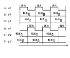
- FIG. 2 is a timing chart showing an example of a control method for the solid-state imaging device of FIG. 1;
- FIG. 4 is a diagram showing a modified example of the schematic configuration of the counter section in FIG. 3 ;
- FIG. 4 is a diagram showing a modified example of the schematic configuration of the counter section in FIG. 3 ;
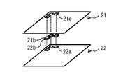
- FIG. 2 is a diagram showing how the solid-state imaging device of FIG. 1 is formed on a laminated substrate;
- 2 is a diagram showing a modified example of the circuit configuration of the pixel in FIG. 1;
- FIG. 2 is a diagram showing a modified example of the circuit configuration of the pixel in FIG. 1;
- FIG. 2 is a diagram showing a modified example of the circuit configuration of the pixel in FIG. 1;
- FIG. 2 is a diagram showing a modified example of the circuit configuration of the pixel in FIG. 1;
- FIG. FIG. 14 is a timing chart showing an example of a control method for a solid-state imaging device having the pixels of FIG. 13;
- FIG. 14 is a diagram showing an example of a circuit configuration of a detection unit in FIG. 13;
- FIG. 14 is a timing chart showing an example of a control method of the detection unit in FIG. 13;
- 2 is a diagram showing a modified example of the circuit configuration of the pixel in FIG. 1;
- FIG. FIG. 18 is a timing chart showing an example of a control method for a solid-state imaging device having the pixels of FIG. 17;
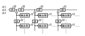
- FIG. 14 is a diagram showing an example of a circuit for inputting a control signal to the detectors of FIGS. 3, 12, and 13;
- FIG. FIG. 14 is a diagram showing an example of a circuit for inputting a control signal to the detectors of FIGS. 3, 12, and 13;
- FIG. 2 is a diagram showing a modified example of the circuit configuration of the pixel in FIG. 1;
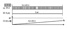
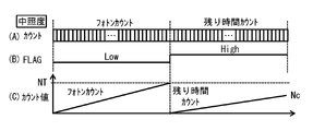
- FIG. FIG. 22 is a timing chart showing an example of a control method for a solid-state imaging device having the pixels of FIG. 21; It is a figure showing the mode of a count when the light of low illumination injects. It is a figure showing the mode of a count when the light of medium illumination intensity injects. It is a figure showing the mode of a count when the light of high illuminance is injected.
- 2 is a diagram showing a modified example of the circuit configuration of the pixel in FIG. 1;
- FIG. FIG. 27 is a diagram for explaining a data pattern in a solid-state imaging device having the pixels of FIG. 26;
- FIG. 27 is a diagram for explaining switch switching in the solid-state imaging device having the pixels of FIG. 26;
- FIG. 27 is a diagram for explaining data output in a solid-state imaging device having the pixels of FIG. 26;
- 2 is a diagram showing a modified example of the circuit configuration of the pixel in FIG. 1;
- FIG. 31 is a diagram for explaining switch switching in the solid-state imaging device having the pixels of FIG. 30.
- FIG. FIG. 31 is a diagram for explaining data output in a solid-state imaging device having the pixels of FIG. 30; It is a figure showing the example of a changed completely type of schematic structure of the solid-state image sensor of FIG. It is a figure showing the example of a changed completely type of schematic structure of the solid-state image sensor of FIG.
- FIG. 2 is a diagram showing a modified example of the circuit configuration of the pixel in FIG. 1;
- FIG. FIG. 36 is a timing chart showing an example of a method of controlling the solid-state imaging device having the pixels of FIG. 35;
- FIG. 36 is a diagram showing a schematic configuration example of the optical pulse response units of FIGS. 3, 4, 7, 8, 10, 12, 13, 17, 21, 26, 30 and 35;
- FIG. 36 is a diagram showing a schematic configuration example of the optical pulse response units of FIGS. 3, 4, 7, 8, 10, 12, 13, 17, 21, 26, 30 and 35;
- FIG. FIG. 2 is a diagram showing an example of factory automation provided with the imaging device of FIG. 1;
- FIG. 2 is a diagram showing an example of a biological sample analyzer equipped with the imaging device of FIG. 1;
- FIG. 1 illustrates an example of functional blocks of an imaging device 100 according to an embodiment of the present disclosure.
- the imaging device 100 is a device that acquires image data by imaging, and includes an optical system 110, a solid-state imaging device 120, a control section 130, and a communication section 140.
- the optical system 110 collects incident light and guides it to the solid-state imaging device 120 .
- the solid-state imaging device 120 acquires image data by imaging, and outputs the image data obtained by imaging to the outside via the communication unit 140 .
- the solid-state imaging device 120 has a plurality of pixels 10, which will be described later. A plurality of pixels 10 are two-dimensionally arranged in the effective pixel area.
- the communication unit 140 is an interface that communicates with an external device, and outputs image data obtained by the solid-state imaging device 120 to the external device.
- the control unit 130 controls the solid-state imaging device 120 to acquire image data by the solid-state imaging device 120 by imaging.
- the control unit 130 performs TDI (Time Delay Integration) control on the solid-state imaging device 120 (a plurality of pixels 10 to be described later).
- the control unit 130 supplies the solid-state imaging device 120 with, for example, a vertical synchronization signal indicating imaging timing and control signals ⁇ 1, ⁇ 2, and ⁇ 3 for controlling the detection unit 12, which will be described later. For example, by simultaneously selecting a plurality of pixels 10 (row line) arranged in the row direction, the control unit 130 transfers the plurality of pixel data obtained in the selected row line to the next stage (next row). ) line.
- the control unit 130 sequentially selects a plurality of row lines at a predetermined cycle.
- a selection period of a plurality of row lines corresponds to an imaging period of the solid-state imaging device 120 .
- the control unit 130 selects a plurality of pixels 10 (row lines) in cycles based on velocity data obtained by the measurement unit. good too.
- the control unit 130 may set the size of the cycle of pixel selection so that the object to be imaged moves by the pixel pitch in the column direction during one cycle of pixel selection.
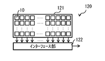
- FIG. 2 shows a schematic configuration example of the solid-state imaging device 120.
- the solid-state imaging device 120 has a TDI sensor and acquires high-sensitivity, low-noise image data.
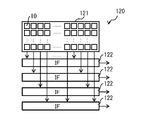
- the solid-state imaging device 120 has, for example, a pixel array section 121 and an interface section 122 as shown in FIG.
- the pixel array section 121 has a plurality of pixels 10 that perform photoelectric conversion. A plurality of pixels 10 are arranged in a matrix in the effective pixel area.
- an object to be imaged moves at a constant speed in, for example, the column direction (vertical direction on the paper surface of FIG. 2) with respect to the pixel array section 121.
- the interface unit 122 acquires, for each column line, the sum of a plurality of pixel data obtained from a plurality of pixels 10 (column line) arranged in the column direction, for example.
- FIG. 3 shows a circuit configuration example of the pixel 10.
- the pixel 10 has, for example, a light pulse response section 11 and a detection section 12 as shown in FIG.
- the optical pulse response section 11 generates an optical pulse in response to incident light.
- the optical pulse response section 11 includes, for example, a light receiving section 11b and a quench section 11a.
- the light receiving section 11b includes an avalanche photodiode (APD).
- APD avalanche photodiode
- a Geiger-mode APD when a voltage higher than the breakdown voltage is applied between terminals, an avalanche phenomenon occurs when a single photon is incident.
- An APD that multiplies a single photon by avalanche phenomenon is called a single photon avalanche diode (SPAD).
- the light pulse response section 11 includes, for example, a SPAD.
- the quenching portion 11a has a function (quenching) of stopping the avalanche phenomenon by lowering the voltage applied to the light receiving portion 11b to the breakdown voltage.
- the quenching section 11a further has a function of allowing the light receiving section 11b to detect photons again by setting the voltage applied to the light receiving section 11b to a bias voltage equal to or higher than the breakdown voltage.
- Quench unit 11a includes, for example, a MOS transistor.
- Quenching portion 11a may be, for example, a resistor.
- One end of the quench section 11a (for example, the source of the MOS transistor) is connected to the power supply line Vdd to which the fixed voltage VDD is applied.
- the other end of the quenching section 11a (for example, the drain of the MOS transistor) is connected to one end of the light receiving section 11b (for example, the cathode of the APD) via the signal line L1.
- the other end of the light receiving section 11b (for example, the cathode of the APD) is connected to a power supply line Vss to which the reference voltage Van is applied, for example.
- the values of the fixed voltage VDD and the reference voltage Van are set so that a voltage equal to or higher than the breakdown voltage is applied to the light receiving portion 11b.
- the signal line L1 is connected to the other end of the quenching portion 11a (for example, the drain of the MOS transistor) and one end of the light receiving portion 11b (for example, the cathode of the APD).
- the detection section 12 includes a counter section 12b.
- the detection section 12 includes a switch section 12a, a counter section 12b, a switch section 12c, a latch section 12d and a switch section 12e.
- the detection section 12 includes a switch section 12a, a counter section 12b, a switch section 12c, and a latch section 12d.
- the detection section 12 may further include a switch section 12e.
- the switch section 12a One end of the switch section 12a is connected to the signal line L1.
- the other end of the switch section 12a is connected to the input terminal of the counter section 12b (input terminal of an addition circuit which will be described later).
- the switch section 12a controls connection/disconnection between the signal line L1 and the input end of the counter section 12b.
- the counter unit 12b is, for example, a k-bit (k ⁇ 1) digital counter as shown in FIG.
- a digital counter is a digital circuit including a latch circuit and the like.
- the counter unit 12b includes a circuit (rewrite circuit) that rewrites the initial value by a signal (rewrite signal) input from the latch unit 12d of the pixel 10 included in the row line of the previous stage (one row before), and a circuit that rewrites the initial value. , and a circuit (adder circuit) for adding the input signal (addition signal) from the optical pulse response unit 11 .
- the switch section 12c is connected to the output terminal of the counter section 12b (the output terminal of the addition circuit).
- the other end of the switch portion 12c is connected to the input end of the latch portion 12d.
- the switch section 12c controls connection/disconnection between the output terminal of the counter section 12b and the input terminal of the latch section 12d.
- the latch unit 12d is, for example, a digital circuit capable of holding k-bit (k ⁇ 1) information as shown in FIG.
- the output terminal of the latch section 12d is connected to one end of the switch section 12e of the pixel 10 included in the row line of the next stage (next row).
- the latch section 12d transfers the held information to the counter section 12b (input terminal of the rewrite circuit) of the pixel 10 included in the next row line via the switch section 12e of the pixel 10 included in the next row line. ).
- the latch section 12d writes the held information as an initial value to the counter section 12b of the pixel 10 included in the next row line.
- One end of the switch portion 12e is connected to the output end of the latch portion 12d of the pixel 10 included in the row line of the previous stage (one row before).
- the other end of the switch section 12e is connected to the input terminal of the counter section 12b (the input terminal of the rewrite circuit).
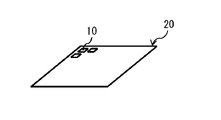
- the solid-state imaging device 120 is formed on one semiconductor substrate 20, for example, as shown in FIG. At this time, an effective pixel area in which a plurality of pixels 10 are arranged in a matrix is formed on the surface of the semiconductor substrate 20 . On the surface of the semiconductor substrate 20, for example, an interface section 122 and the like are mounted around the effective pixel area.
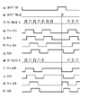
- FIG. 6 is a timing chart showing an example of the solid-state imaging device 120 control method.
- the control unit 130 turns on the switch unit 12a of each pixel 10 by setting the control signal ⁇ 1 to High.
- photons are input from the light receiving section 11b in which the avalanche phenomenon is occurring to the counter section 12b.
- the control section 130 turns off the switch section 12a of each pixel 10 by setting the control signal ⁇ 1 to low when a predetermined exposure period has elapsed. This stops the input of photons from the light receiving section 11b to the counter section 12b.
- the counter section 12b information corresponding to the number of input photons is added to the initial value, and information obtained thereby (holding information) is held.
- the control section 130 turns on the switch section 12c of each pixel 10 by setting the control signal ⁇ 2 to High.
- the counter section 12b outputs information (held information) held in the counter section 12b to the latch section 12d via the switch section 12c.
- the latch section 12d retains information (held information) input from the counter section 12b.
- the control section 130 turns off the switch section 12c of each pixel 10 by setting the control signal ⁇ 2 to low.
- the control section 130 turns on the switch section 12e of each pixel 10 by setting the control signal ⁇ 3 to High.
- the latch section 12d outputs information (held information) held in the latch section 12d to the counter section 12b via the switch section 12e.
- the counter section 12b holds the information (holding information) input from the latch section 12d as an initial value.
- the control unit 130 writes the information held in the counter unit 12b as an initial value into the counter unit 12b included in the next-stage pixel 10 in the column direction.
- the information corresponding to the optical pulse obtained from is added to the initial value.
- the control unit 130 writes the information input from the counter unit 12b held in the latch unit 12d as an initial value to the counter unit 12b included in the next pixel 10 in the column direction.
- control unit 130 outputs to the interface unit 122 the sum of a plurality of pixel data obtained from a plurality of pixels 10 (column lines) arranged in the column direction for each column line.
- the information held in the counter section 12b in each pixel 10 is written as an initial value to the counter section 12b included in the row line of the next stage (next row). Accordingly, the information obtained from the optical pulse response section 11 is added to the initial value of the counter section 12b. As a result, the information held in the counter section 12b after the addition is written as an initial value to the counter section 12b included in the row line of the next stage (next row). As a result, addition processing can be performed without performing AD conversion processing. In addition, since the pixel data obtained in this way is low-noise data, there is no need to perform CDS processing. Therefore, it is possible to provide the imaging apparatus 100 that does not require AD conversion processing or CDS processing.
- the update frequency of the high-order bit counter is low.
- the operating frequency is also low for the switches connected to the upper bits of the counter section 12b.
- the latch section 12d the operating frequency of the latches connected to the upper bits of the counter section 12b is also low.
- the switch section 12e the operating frequency is also low for the switches connected to the upper bits of the counter section 12b.
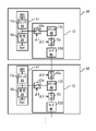
- the upper bits of the counter section 12b and the portions of the switch section 12c, the latch section 12d, and the switch section 12e connected to the higher bits of the counter section 12b are shown in FIG. As described above, it may be formed outside the region where the pixel array section 121 is formed (out-of-array region R2) in the solid-state imaging device 120 . At this time, the bits other than the high-order bits of the counter section 12b and the portions of the switch section 12c, the latch section 12d, and the switch section 12e connected to the bits other than the high-order bits of the counter section 12b are shown in FIG.
- the pixel array section 121 may be formed in the formation region (array region R1) of the pixel array section 121 in the solid-state imaging device 120 .
- the area of the array region R1 can be reduced.
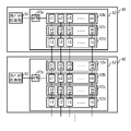
- the number of bits of the counter section 12b, the switch section 12c, the latch section 12d and the switch section 12e is, for example, as shown in FIG.
- the rear stage of the column line may be configured to be larger.
- the solid-state imaging devices 120 may be dispersedly formed on a plurality of laminated semiconductor substrates.
- the solid-state imaging devices 120 may be dispersedly formed on two laminated semiconductor substrates 21 and 22 .
- a portion of each pixel 10 other than the light receiving portion 11b (hereinafter referred to as “circuit 21a”) may be formed on the first semiconductor substrate 21 .
- a portion including the light receiving portion 11 b (hereinafter referred to as “circuit 22 a ”) may be formed on the second semiconductor substrate 22 .
- the circuit 21a and the circuit 22a may be electrically connected by, for example, joining the pad electrode 21b connected to the circuit 21a and the pad electrode 22b connected to the circuit 22a to each other.
- the light pulse response unit 11 of each pixel 10 includes, for example, a plurality of sub-pixels 11-1 and outputs of the plurality of sub-pixels 11-1, as shown in FIG. It may have an addition unit 11-2 connected thereto.
- Each sub-pixel 11-1 has a quenching portion 11a, a light receiving portion 11b and a pulse generating portion 11c.
- the pulse generator 11c is connected to the signal line L1, and the photons output from the light receiver 11b are input to the pulse generator 11c.
- the pulse generating section 11c generates a pulse for the photons input from the light receiving section 11b, and outputs the pulse to the adding section 11-2.
- the adder 11-2 counts the pulses input from the plurality of sub-pixels 11-1, and outputs to the detector 12 the number of pulses corresponding to the obtained count value. In this manner, an image with high sensitivity can be obtained by using a plurality of sub-pixels 11-1 and addition units 11-2.
- the pulse generator 11c may be omitted, for example, as shown in FIG.
- the adder 11-2 counts the photons input from each sub-pixel 11-1, and outputs the number of pulses corresponding to the obtained count value to the detector 12.
- FIG. Even in this case, an image with high sensitivity can be obtained by using the pixel data obtained by the addition by the addition section 11-2.
- the latch section 12d and the switch section 12c may be omitted for each pixel 10 of the odd-numbered lines. Even in this case, the control unit 130 controls the solid-state imaging device 12 at the timing shown in FIG. be able to.
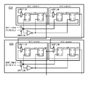
- FIG. 15 shows an example of the circuit configuration of the detection section 12A.
- the detection unit 12A includes a plurality of 1-bit counters connected in series and a multiplexer (hereinafter referred to as “ (referred to as a "first multiplexer”) and a NOT circuit.
- the 1-bit counter includes, for example, a D flip-flop consisting of a plurality of (two) D-latches, and a multiplexer (hereinafter referred to as a "second multiplexer") connected to the data input terminals of the D flip-flops. It is configured. That is, the detector 12A has a D flip-flop for each bit.
- the output of the first multiplexer is input as the clock of the D latch in the preceding stage of the D flip-flop.
- An output obtained by inverting the output of the first multiplexer (output of the NOT circuit) is input as a clock of the D latch in the subsequent stage of the D flip-flop.
- the first multiplexer receives the output of the D flip-flop in the same stage (same row) as the first multiplexer and the output of the D flip-flop included in the previous stage (previous row) row line.
- Each pixel 10 may have a plurality of detectors 12 in the above embodiment and its modification.
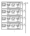
- Each pixel 10 may have, for example, two detectors 12 and an adder 16 that adds the output values of the two detectors 12, as shown in FIG.
- the two detection units 12 are connected to the common light pulse response unit 11, and in the plurality of pixels 10 included in the column line, one detection unit 12 is connected in a row, and the other detection unit 12 is connected in a row. Sections 12 are also connected in a row.
- the control unit 130 sets the information held in one of the detection units 12 (hereinafter referred to as the “detection unit 12L”) as an initial value to the detection unit 12L included in the next pixel 10 in the column direction.
- the information held in the other detection unit 12 (hereinafter referred to as "detection unit 12R”) is initialized to the detection unit 12R included in the pixel 10 at the next stage in the column direction. be written as a value.
- the control unit 130 performs exposure by dividing it into a front stage and a rear stage in one line period. For example, after the former stage exposure (during the latter stage exposure), the control section 130 sequentially outputs the control signals ⁇ 2 and ⁇ 3 to one detection section 12 of the plurality of pixels 10 included in the column line. Further, for example, after the latter exposure (during the former exposure), the control section 130 sequentially outputs control signals ⁇ 2' and ⁇ 3' to the other detection section 12 of the plurality of pixels 10 included in the column line. By doing so, it is possible to greatly reduce the non-exposure time compared to the case where only the preceding stage is exposed in one line cycle as in the above embodiment. As a result, the imaging device 100 with higher sensitivity can be provided.
- a repeater 31 may be provided at a predetermined portion of the wiring.
- the repeater 31 is inserted in wiring through which control signals input from the control unit 130 to the plurality of pixels 10 are propagated.
- a shift register 32 may be provided in place of the repeater 31 at a predetermined portion of the wiring.
- each detection unit 12 may have an OF determination unit 12h that determines whether or not the counter unit 12b is saturated, as shown in FIG. 21, for example.
- each pixel 10 included in the second and subsequent row lines for example, as shown in FIG. It includes an OF determination section 12h and latch sections 12d and 12j.
- each pixel 10 included in the first row line for example, as shown in FIG. It includes portions 12d and 12j.
- One end of the switch section 12a is connected to the signal line L1.
- the other end of the switch section 12a is connected to the input end of the multiplexer 12f.
- the switch unit 12a controls connection/disconnection between the signal line L1 and the input terminal of the multiplexer 12f.
- the input end of the multiplexer 12f is connected to the other end of the switch section 12a and the wiring to which the clock CLK is input.
- the output end of the multiplexer 12f is connected to the input end of the counter section 12b (the input end of the adder circuit).
- the switch section 12i One end of the switch section 12i is connected to the output terminal of the OF determination section 12h (the output terminal of the addition circuit described later). The other end of the switch portion 12i is connected to the input end of the latch portion 12j.
- the switch section 12i controls connection/disconnection between the output terminal of the OF determination section 12h (the output terminal of the adder circuit) and the input terminal of the latch section 12j.
- the latch unit 12j is, for example, a digital circuit capable of holding m-bit (m ⁇ 1) information.
- the output terminal of the latch section 12j is connected to one end of the switch section 12g of the pixel 10 included in the row line of the next stage (next row).
- the latch section 12j outputs the held information to the OF determination section 12h of the pixel 10 included in the next row line via the switch section 12g of the pixel 10 included in the next row line.
- the latch section 12d writes the held information as an initial value to the counter section 12b of the pixel 10 included in the next row line.
- One end of the switch section 12g is connected to the output terminal of the latch section 12j of the pixel 10 included in the row line of the previous stage (one row before).
- the other end of the switch section 12g is connected to the input terminal of the OF determination section 12h (the input terminal of the rewriting circuit).
- the multiplexer 12f outputs photons input via the switch unit 12a to the counter unit 12b.
- the counter unit 12b counts photons.
- the multiplexer 12f outputs the clock CLK input from the wiring to the counter unit 12b.
- the counter unit 12b counts the clock CLK.
- the counter unit 12b resets the counter and starts counting the clock CLK, for example, when FLAG that changes from Low level to High level is input from the OF determination unit 12h.
- the counter unit 12b resets the counter and starts counting photons, for example, when FLAG that changes from High level to Low level is input from the OF determination unit 12h.
- the OF determination section 12h When the count value of the counter section 12b is equal to or less than a predetermined threshold value, the OF determination section 12h outputs, for example, a Low level FLAG to the multiplexer 12f, the counter section 12b and the switch section 12i. When the count value of the counter section 12b exceeds a predetermined threshold value, the OF determination section 12h outputs, for example, a High level FLAG to the multiplexer 12f, the counter section 12b and the switch section 12i.
- the OF determination unit 12h further determines saturation of the counter unit 12b based on information input from the latch unit 12j of the pixel 10 included in the previous row (previous row) through the switch unit 12g. . For example, when a Low-level FLAG is input through the switch unit 12g, the OF determination unit 12h determines that the counter unit 12b has not been saturated in the previous stage (one row before), and outputs a Low-level FLAG. is output to the multiplexer 12f, the counter section 12b and the switch section 12i. For example, when a High-level FLAG is input via the switch unit 12g, the OF determination unit 12h determines that the counter unit 12b has already been saturated in the preceding stage (one row before), and outputs a High-level FLAG. is output to the multiplexer 12f, the counter section 12b and the switch section 12i.
- FIG. 22 is a timing chart showing an example of a control method for the solid-state imaging device 120 having the pixels 10 of FIG.
- the control unit 130 turns on the switch unit 12a of each pixel 10 by setting the control signal ⁇ 1 to High.
- the control section 130 turns off the switch section 12a of each pixel 10 by setting the control signal ⁇ 1 to low when a predetermined exposure period has elapsed. This stops the input of photons from the light receiving section 11b to the counter section 12b.
- the counter section 12b information corresponding to the number of input photons is added to the initial value, and information obtained thereby (holding information) is held.
- the control unit 130 turns on the switch units 12c and 12i of each pixel 10 by setting the control signal ⁇ 2 to High.
- the counter section 12b outputs information (held information) held in the counter section 12b to the latch section 12d via the switch section 12c.
- the latch section 12d retains information (held information) input from the counter section 12b.
- the OF determination unit 12h outputs information (held information) held in the OF determination unit 12h to the latch unit 12j via the switch unit 12i.
- the latch section 12j retains information (held information) input from the OF determination section 12h.
- the control unit 130 turns off the switch units 12c and 12i of each pixel 10 by setting the control signal ⁇ 2 to low. Subsequently, the control unit 130 turns on the switch units 12e and 12g of each pixel 10 by setting the control signal ⁇ 3 to High. As a result, the latch section 12d outputs information (held information) held in the latch section 12d to the counter section 12b via the switch section 12e.
- the counter section 12b holds the information (holding information) input from the latch section 12d as an initial value.
- the latch section 12j outputs information (held information) held in the latch section 12j to the OF determination section 12h via the switch section 12g.
- the control unit 130 outputs to the interface unit 122 the sum of a plurality of pixel data obtained from a plurality of pixels 10 (column lines) arranged in the column direction for each column line.
- interface section 122 outputs Nc to the outside via communication section 140 as integrated value N.
- the interface unit 122 outputs the value obtained by using the following formula as the integrated value N to the outside via the communication unit 140 .
- the exposure time (remaining time) after the counter section 12b is saturated is measured by counting the clock CLK with the counter section 12b.
- the saturation timing of the counter section 12b is advanced as the illuminance of the incident light increases, as shown in FIGS. 23, 24, and 25, for example.
- the counter section 12b counts the clock CLK instead of counting photons.
- the count value of the clock CLK in the counter section 12b increases as the illuminance of the incident light increases.
- the clock CLK count value increases as the remaining time increases.
- the exposure time Texp in one frame period is divided by the remaining time Tc to obtain It is possible to obtain the sum of the pixel data of the column lines.
- the dynamic range of the detection unit 12 can be expanded by counting the clock CLK during the remaining time.
- a detection unit 13 may be provided instead of the detection unit 12.
- the detection section 13 has a switch section 13a and a counter section 13b.
- the switch section 13a has the same number of input terminals as the number of pixels 10 included in the column line.
- FIG. 26 illustrates how eight input terminals are provided.
- each input terminal is connected to different optical pulse response sections 11 included in the column lines.
- the output terminal of the switch section 13a is connected to the input terminal of the counter section 13b.
- the counter unit 13b is, for example, a k-bit (k ⁇ 1) digital counter.
- a digital counter is a digital circuit including a latch circuit and the like.
- the counter section 13b includes a circuit (integration circuit) that integrates the input signal from the switch section 13a.
- An output terminal of the counter section 13 b is connected to the interface section 122 .
- FIG. 27 conceptually illustrates an example of data pattern switching for each horizontal period in the imaging area of the solid-state imaging device 120 .
- p0 to p7 are codes assigned to the plurality of optical pulse response sections 11 included in the column lines.
- FIG. 27 suggests that a plurality of objects aligned in the column direction move in the imaging region in the column direction at a speed equal to the line rate.
- FIG. 28 conceptually illustrates an example of switch switching for each horizontal period of the counter section 13b.
- the control section 130 controls all the optical pulse response sections 11 included in the column line for each switch section 13a included in the column line in one frame period.
- Control signals ⁇ a to ⁇ h are output to the column lines so that they are sequentially selected one by one.
- the control unit 130 causes the switch unit 13a to sequentially select all the optical pulse response units 11 included in the column line, one by one, so that information corresponding to the optical pulses obtained from all the optical pulse response units 11 can be obtained.
- the counter unit 13b is made to perform the integration.
- FIG. 29 conceptually represents the pixel data output from each counter section 13b included in the column line as a result of the switch switching shown in FIG.
- each counter unit 13b included in the column line has information (holding information) corresponding to the number of photons input from all the light pulse response units 11 included in the column line at hatched timings. to the interface unit 122 .
- This hold information corresponds to the sum of a plurality of pixel data obtained from the column lines.
- each counter unit 13b included in the column line outputs information ( held information) to the interface unit 122 .
- each counter unit 13b included in the column line acquires the sum of pixel data obtained from each pixel 10 included in the column line, and outputs the sum to the interface unit 122.
- addition processing in a column line can be performed by each counter section 13b included in the column line.
- the pixel data obtained in this way is low-noise data, there is no need to perform CDS processing. Therefore, it is possible to provide the imaging apparatus 100 that does not require AD conversion processing or CDS processing.
- the solid-state imaging device 120 has, for example, as shown in FIG. 30, a plurality of column lines each including "a plurality of pixels 10 provided with a detection unit 13" arranged in the column direction. may At this time, the solid-state imaging device 120 sets the transfer unit 14 to 1 to transfer the sum of the pixel data obtained in the first column line as the initial value of the detection unit 13 (counter unit 13b) of the next column line. It may be provided for each pixel 10 included in the column line of the tier.
- the transfer section 14 has, for example, two switch sections 14a and 14c and a latch section 14b.
- the switch portion 14a One end of the switch portion 14a is connected to the output end of the detection portion 13 of the corresponding pixel 10. The other end of the switch portion 14a is connected to the input end of the latch portion 14b.
- the switch section 12i controls connection/disconnection between the output terminal of the detection section 13 and the input terminal of the latch section 14b of the corresponding pixel 10 .
- the latch unit 14b is, for example, a digital circuit capable of holding m-bit (m ⁇ 1) information.
- the output terminal of the latch section 14b is connected to one end of the switch section 14c.
- the latch section 14b outputs the held information as an initial value to the detection section 13 (counter section 13b) of the corresponding pixel 10 included in the next column line via the switch section 14c.
- One end of the switch portion 14c is connected to the output end of the latch portion 14b.
- the other end of the switch section 14c is connected to the detection section 13 (the input terminal of the rewrite circuit of the counter section 13b) of the corresponding pixel 10 included in the next column line.
- the counter section 13b included in the detection section 13 is, for example, a k-bit (k ⁇ 1) digital counter.
- a digital counter is a digital circuit including a latch circuit and the like.
- the counter unit 13b includes a circuit (rewrite circuit) that rewrites the initial value by a signal (rewrite signal) input from the latch unit 14b included in the corresponding transfer unit 14, and a circuit (rewrite circuit) that rewrites the initial value based on the input from the light pulse response unit 11 for the initial value. and a circuit (adder circuit) for adding the signals (addition signal).
- FIG. 31 conceptually illustrates an example of switch switching for each horizontal period of the counter section 13b.
- the control section 130 controls all the optical pulse response sections 11 included in the column line for each switch section 13a included in the column line in one frame period.
- Control signals ⁇ a to ⁇ d are output to the respective column lines so that they are sequentially selected one by one.
- FIG. 32 conceptually represents the pixel data output from each counter section 13b included in the column line as a result of the switch switching shown in FIG.
- each counter unit 13b included in the column line has information (holding information) corresponding to the number of photons input from all the light pulse response units 11 included in the column line at hatched timings. is output to the transfer unit 14 (the interface unit 122 at the final stage).
- This hold information corresponds to the sum of a plurality of pixel data obtained from the column lines.
- the transfer unit 14 stores the sum of the pixel data obtained in the first column line as the initial value of the detection unit 13 (counter unit 13b) of the next column line. Transfer as
- the information held in the counter section 13b in each column line is written as an initial value to the counter section 13b included in the next column line, and Information obtained from the optical pulse response unit 11 is added to the initial value of the counter unit 13b.
- the information held in the counter section 13b after the addition is written as the initial value to the counter section 13b included in the next column line.
- addition processing can be performed without performing AD conversion processing.
- the pixel data obtained in this way is low-noise data, there is no need to perform CDS processing. Therefore, it is possible to provide the imaging apparatus 100 that does not require AD conversion processing or CDS processing.
- the solid-state imaging device 120 may have a plurality of interface units 122 as shown in FIG. 33, for example.
- Each interface unit 122 processes, for example, data of a plurality of column lines assigned to each interface unit 122 (the sum of a plurality of pixel data obtained from the column lines). In this case, compared to the case where one interface unit 122 processes data for all column lines, the speed of processing data for all column lines is improved.
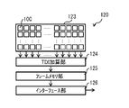
- the solid-state imaging device 120 may have a pixel array section 123, a TDI addition section 124, a frame memory section 125, and an interface section 126, for example, as shown in FIG. good.
- the pixel array section 123 has a plurality of pixels 10C that perform photoelectric conversion.
- a plurality of pixels 10C are arranged in a matrix in the effective pixel area.
- the object to be imaged moves at a constant speed in the column direction (vertical direction in FIG. 34) with respect to the pixel array section 123, for example.
- FIG. 35 shows a circuit configuration example of the pixel 10C.
- a plurality of vertical signal lines VSL are provided, one for each of a plurality of pixels 10C (column lines) arranged in the column direction.
- the pixel 10C has, for example, a light pulse response section 11 and a detection section 12C as shown in FIG.
- the optical pulse response section 11 generates an optical pulse in response to incident light.
- the optical pulse response section 11 has, for example, the same configuration as in the above embodiment and its modification.
- the detection section 12C includes, for example, a switch section 12a, a counter section 12b and a switch section 12k.
- One end of the switch section 12 a is connected to the signal line L 1 of the optical pulse response section 11 .
- the other end of the switch section 12a is connected to the input terminal of the counter section 12b (the input terminal of the integration circuit described later).
- the switch section 12a controls connection/disconnection between the signal line L1 and the input end of the counter section 12b.
- the counter unit 12b is, for example, a k-bit (k ⁇ 1) digital counter as shown in FIG.
- a digital counter is a digital circuit including a latch circuit and the like.
- the counter section 12b includes a circuit (integration circuit) that integrates the input signal from the optical pulse response section 11.
- FIG. One end of the switch section 12c is connected to the output terminal of the counter section 12b (the output terminal of the integrating circuit).
- the other end of the switch section 12c is connected to the vertical signal line VSL, and is connected to the TDI addition section 124 via the vertical signal line VSL.
- the control unit 130 performs TDI control on the solid-state imaging device 120 (the plurality of pixels 10C, the TDI addition unit 124, the frame memory 125, and the interface unit 126).
- the control unit 130 outputs a plurality of pixel data obtained from the selected row lines to a plurality of vertical signal lines VSL. output to the TDI adder 124 via the At this time, the control unit 130 sequentially selects a plurality of row lines at a predetermined cycle.
- the TDI addition unit 124, the frame memory unit 125, and the interface unit 126 provide a plurality of pixel lines (row lines) obtained from a plurality of sets of pixel lines (row lines) arranged side by side in the row direction among the plurality of pixels 10C.
- Image data is generated by performing TDI processing using a pulse signal.
- the TDI addition unit 124 acquires a plurality of pixel data (a plurality of pixel data in the i-th row) input from the i-th row line selected by the control unit 130 via the plurality of vertical signal lines VSL. .
- the TDI adder 124 writes the acquired plurality of pixel data of the i-th row to the memory of the predetermined row address (i-th row) of the frame memory unit 125 . For example, each time a plurality of pieces of pixel data are acquired, the TDI addition unit 124 writes the acquired pieces of pixel data to the row address of the line next to the previously written row address in the frame memory unit 125 . The TDI addition unit 124 writes the acquired plural pixel data to the memory of the first (first row) row address when writing to the row address of the last row (nth row) was previously performed. . The TDI adder 124 performs such write processing until it acquires a plurality of pieces of pixel data corresponding to the number of row lines.
- the TDI addition unit 124 Each time the TDI addition unit 124 acquires pixel data from all the pixels 10C in the pixel array unit 123, the TDI addition unit 124 selects a place to add a plurality of pixel data of the i-th row acquired thereafter to the frame memory unit 125 as m. Shift line by line (for example, by one line).
- the TDI adder 124 adds, for example, the acquired pixel data of the i-th row to the memory at a predetermined row address (i+t ⁇ m-th row) in the frame memory unit 125 . t corresponds to the number of times the pixel data is acquired from all the pixels 10C.
- each memory of the frame memory unit 125 stores the sum of a plurality of (n) pixel data obtained from the column lines.
- the interface unit 126 acquires one frame of pixel data (that is, image data) from the frame memory unit 125 .
- the interface unit 126 outputs the acquired image data to the outside via the communication unit 140 .
- FIG. 36 is a timing chart showing an example of the solid-state imaging device 120 control method according to this modification.
- the control unit 130 turns on the switch unit 12a of each pixel 10C by setting the control signal ⁇ 1 to High.
- photons are input from the light receiving section 11b in which the avalanche phenomenon is occurring to the counter section 12b.
- the control section 130 turns off the switch section 12a of each pixel 10C by setting the control signal ⁇ 1 to low when a predetermined exposure period has elapsed. This stops the input of photons from the light receiving section 11b to the counter section 12b.
- the counter unit 12b accumulates information corresponding to the number of input photons, and holds the information obtained thereby (holding information).
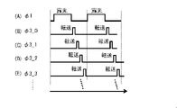
- control unit 130 sequentially changes the control signals ⁇ 3_0 to ⁇ n ⁇ 1 from High to Low one by one during the period of one exposure cycle (one scan period), thereby switching the switch unit 12c of each pixel 10C to the row line. turn on and off sequentially.
- the counter section 12b outputs the information (held information) held in the counter section 12b to the TDI addition section 124 via the switch section 12c.
- the TDI adder 124 writes the acquired plurality of pixel data of the i-th row to the memory of the predetermined row address (i-th row) of the frame memory unit 125 .
- the TDI addition unit 124 each time the TDI addition unit 124 acquires a plurality of pixel data from the row line in which the switch unit 12c is turned on and off, the TDI addition unit 124 stores the acquired plurality of pixel data in the frame memory unit 125 at the address next to the previously written row address. Write to the row address of the line. The TDI addition unit 124 writes the acquired plural pixel data to the memory of the first (first row) row address when writing to the row address of the last row (nth row) was previously performed. . The TDI adder 124 performs such write processing until all the switches 12c are turned on and off.
- control unit 130 changes the control signal ⁇ 1 from High to Low every time one scanning period elapses, thereby causing each light receiving unit 11b to perform exposure.
- the control unit 130 sequentially turns the control signals ⁇ 3_0 to ⁇ n ⁇ 1 from High to Low one by one in each scanning period, thereby sequentially turning on/off the switch unit 12c of each pixel 10C for each row line.
- the TDI adding unit 124 shifts the addition location of the acquired plurality of pixel data of the i-th row to the frame memory unit 125 by m rows (for example, one row) in each scanning period.
- the TDI adder 124 adds, for example, the acquired pixel data of the i-th row to the memory at a predetermined row address (i+t ⁇ m-th row) in the frame memory unit 125 .
- Control unit 130 causes interface unit 126 to output the acquired image data to the outside via communication unit 140 .
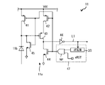
- the optical pulse response section 11 may have an active precharge type circuit as shown in FIG. 37, for example.
- the optical pulse response section 11 shown in FIG. 37 has a light receiving section 11 b, transistors 41 , 42 , 43 , 44 and 45 , an inverter 46 and a pulse generator 47 .
- the pulse generator 47 has a delay device D3 and a NAND circuit NP as internal components.
- Transistors 41, 42 and 43 are PMOS transistors.
- Transistors 44 and 45 are NMOS transistors.
- the gates of the transistors 41, 42, 44 and 45 are connected to the output terminal of the NAND circuit NP via signal lines.
- the sources of the transistors 41 and 42 are connected to the power supply line Vdd.
- the drain of the transistor 41 is connected to the gate of the transistor 43, the source of the transistor 45, and one end of the light receiving portion 11b (for example, the cathode of the photodiode) via signal lines.
- the drains of transistors 44 and 45 are connected to the ground line.
- the source of transistor 43 is connected to the drain of transistor 42 .
- the drain of transistor 43 is connected to the input terminal of inverter 46 and the source of transistor 44 via a signal line.
- An output end of the inverter 46 is connected to the signal line L1.
- the delay device D3 is connected to the signal line L1 and one input terminal of the NAND circuit NP.
- the other input terminal of the NAND circuit NP is connected to the terminal xRST.
- the pulse generator 47 is not limited to the configuration described above, and may have a configuration different from the configuration described above.
- the operation of the optical pulse response section 11 will be described.
- the light receiving portion 11b reacts with photons, the current between the cathode and the anode increases, the current between the source and the drain of the transistor 41 increases, and the voltage drop between the source and the drain of the transistor 41 causes the gate voltage of the transistor 43 to drop. becomes Low.
- both transistors 41 and 43 are turned on. Accordingly, the current flowing between the source and drain of the transistor 42 increases. Therefore, the gate-source voltage of the transistor 42 increases due to the Id-Vgs characteristic.
- the light pulse response unit 11 outputs a Low (negative polarity) pulse to the signal line L1 when detecting photons.
- the optical pulse response section 11 is a circuit that performs active quenching.
- the source-drain is turned off, and the through current from the power supply to the ground is suppressed. Therefore, the voltage at the input terminal of inverter 46 is initialized by the potential of the ground line and becomes Low.
- the inverter 46 outputs a High voltage to the signal line L1.
- the voltage of one input terminal of the NAND circuit NP becomes High with a delay caused by the delay device D3.
- the NAND circuit NP outputs a Low voltage. At this time, a low voltage is applied to the gate of the transistor 41, so that the source-drain of the transistor 41 is turned on.
- the potential of the cathode of the light receiving section 11b is raised by the voltage of the power supply line Vdd. Since the voltage across the terminals of the light receiving section 11b becomes equal to or higher than the breakdown voltage, the light pulse response section 11 becomes able to detect photons again.
- the cathode of the light receiving section 11b when a signal corresponding to photons is output from the signal line L1, the cathode of the light receiving section 11b is connected to the ground potential, so high-speed quenching can be performed. Moreover, since the transistor 41 is also driven by the pulse, the cathode voltage of the light receiving section 11b is also raised in a short time compared to the case where the current source transistor is used. In addition, the optical pulse response unit 11 according to this modification can output a pulse with a constant width to the subsequent circuit regardless of the length of the recharge time. In addition, the optical pulse response unit 11 according to this modification has good input/output characteristics at high illuminance.
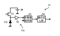
- the optical pulse response section 11 may have an active recharge type circuit as shown in FIG. 38, for example.
- the optical pulse response section 11 shown in FIG. 38 has a light receiving section 11b, a transistor 51, an amplifier 52, a count value holding section 53, and a reading section .
- a circuit composed of the transistor 51, the amplifier 52, the count value holding section 53 and the reading section 54 is a circuit corresponding to the quench section 11a.
- a power supply voltage VR is connected to the drain of the transistor 51, a reset pulse signal is applied to the gate of the transistor 51, and the cathode of the light receiving section 11b is connected to the source of the transistor 51.
- the anode of the light receiving portion 11b is connected to the ground line.
- the cathode of the light receiving section 11b is connected to the input terminal of the amplifier 52, and the output terminal of the amplifier 52 is connected to one input terminal (clock input terminal) of the count value holding section 53.
- FIG. An initialization pulse signal is applied to the other input terminal (initialization terminal) of the count value holding unit 53 .
- the cathode potential of the light receiving portion 11b decreases due to the photoelectric conversion effect.
- the transistor 51 is turned on by a reset pulse signal applied to the gate of the transistor 51, the cathode potential of the light receiving section 11b rises to the power supply reduced voltage VR. This rising change to the reduced voltage VR is amplified by the amplifier 52 and input to the count value holding unit 53 .
- the count value holding unit 53 holds the value obtained by counting the pulses obtained from the amplifier 52 as follows. For example, a reset pulse signal is applied to the transistor 51 at arbitrary intervals. On the other hand, assume that a plurality of incident photons enter the light receiving section 11b during a period (measurement period) longer than the period of the reset pulse signal. At this time, if the measurement period is segmented by the period of the reset pulse signal, information on the presence or absence of incident photons can be obtained for each segment. The incident photon presence/absence information does not indicate how many reset pulse signals exist, but information on whether or not there is a reset pulse signal. In a section in which there were no incident photons, no pulse is output from the amplifier 52 even if the transistor 51 is turned on.
- the counting unit 54 reads the count value held in the count value holding unit 53 from the count value holding unit 53 and outputs it to the detection unit 12 . do.
- the optical pulse response section 11 may have a passive recharge type circuit.
- the plurality of light receiving sections 11b included in the column lines of the pixel array sections 121 and 123 may be configured to detect light in a common wavelength band.
- the plurality of light receiving portions 11b included in the column lines of the pixel array portions 121 and 123 for example, use color filters that transmit light in a common wavelength band as the light incident surface of the photodiode. You may have it on.
- the interface units 122 and 126 can obtain the sum of multiple pixel data of the same color for each column line.
- the plurality of light receiving units 11b included in the first column line emit red light.
- the plurality of light receiving sections 11b included in the second column line are configured to detect green light
- the plurality of light receiving sections 11b included in the third column line are configured to detect It may be configured to detect blue light.
- the interface units 122 and 126 can obtain the sum of red pixel data, the sum of green pixel data, and the sum of blue pixel data for each column line group. As a result, the interface units 122 and 126 can generate and output image data that can be displayed in color.
- imaging device 100 (hereinafter simply referred to as “imaging device 100”) according to the above-described embodiment and modifications thereof will be described.
- FIG. 34 shows a schematic configuration example of FA (factory automation) using the imaging device 100 .
- an imaging device 100 is arranged near a conveying device 300 including a belt conveyor, and images a predetermined imaging area of the belt conveyor. In the imaging area, a plurality of articles are moving in the traveling direction of the belt conveyor by the belt conveyor.
- the imaging device 100 outputs image data obtained by imaging to the signal processing section 200 .
- the signal processing unit 200 inspects the presence or absence of defects in the article included in the image data.
- FIG. 35 shows a schematic configuration example of a biological sample analyzer 6100 using the imaging device 100 as a detection unit 6102, which will be described later.
- the biological sample analyzer 6100 shown in FIG. 35 includes a light irradiation unit 6101 that irradiates light onto the biological sample S flowing through the channel C, a detection unit 6102 that detects light generated by irradiating the biological sample S with light, and an information processing unit 6103 that processes information about light detected by the detection unit 6102 .
- Examples of the biological sample analyzer 6100 include flow cytometers and imaging cytometers.
- the biological sample analyzer 6100 may include a sorting section 6104 that sorts out specific biological particles P in the biological sample S.
- a cell sorter can be given as an example of the biological sample analyzer 6100 including the sorting section 6104 .
- the biological sample S may be a liquid sample containing biological particles P.
- Bioparticles P are, for example, cellular or non-cellular bioparticles.
- the cells may be living cells, and more specific examples include blood cells such as red blood cells and white blood cells, and germ cells such as sperm and fertilized eggs.
- the cells may be directly collected from a specimen such as whole blood, or may be cultured cells obtained after culturing.
- Examples of the noncellular bioparticles include extracellular vesicles, particularly exosomes and microvesicles.
- the bioparticle P may be labeled with one or more labeling substances (for example, a dye (especially a fluorescent dye) and a fluorescent dye-labeled antibody). Note that particles other than the biological particles P may be analyzed by the biological sample analyzer of the present disclosure, and beads or the like may be analyzed for calibration or the like.
- the channel C is configured so that the biological sample S flows.
- the flow path C can be configured such that a flow in which the biological particles P contained in the biological sample S are arranged substantially in a line is formed.
- a channel structure including channel C may be designed to form a laminar flow.
- the channel structure is designed so that a laminar flow is formed in which the flow of the biological sample S (sample flow) is surrounded by the flow of the sheath liquid.
- the design of the flow channel structure may be appropriately selected by those skilled in the art, and known ones may be adopted.
- the channel C may be formed in a flow channel structure such as a microchip (a chip having channels on the order of micrometers) or a flow cell.
- the width of the channel C may be 1 mm or less, and particularly 10 ⁇ m or more and 1 mm or less.
- the channel C and the channel structure including it may be made of a material such as plastic or glass.
- the biological sample analyzer 6100 is configured such that the biological sample S flowing in the flow path C, particularly the biological particles P in the biological sample S, is irradiated with light from the light irradiation unit 6101 .
- the biological sample analyzer 6100 may be configured such that the light irradiation point (interrogation point) for the biological sample S is in the flow channel structure in which the flow channel C is formed, or the light irradiation point may be configured to be outside the channel structure.
- the former there is a configuration in which the light is applied to the channel C in the microchip or the flow cell. In the latter, the light may be applied to the biological particles P after exiting the flow path structure (especially the nozzle section thereof).
- the light irradiation unit 6101 includes a light source unit that emits light and a light guide optical system that guides the light to the irradiation point.
- the light source section includes one or more light sources.
- the type of light source is, for example, a laser light source or an LED.
- the wavelength of light emitted from each light source may be any wavelength of ultraviolet light, visible light, or infrared light.
- the light guiding optics include optical components such as beam splitter groups, mirror groups or optical fibers. Also, the light guide optics may include a lens group for condensing light, for example an objective lens. There may be one or more irradiation points where the biological sample and the light intersect.
- the light irradiation unit 6101 may be configured to condense light irradiated from one or different light sources to one irradiation point.
- the detection unit 6102 includes at least one photodetector that detects light generated by irradiating the biological particles P with light.
- the light to be detected is, for example, fluorescence or scattered light (eg, any one or more of forward scattered light, backscattered light, and side scattered light).
- Each photodetector includes one or more photodetectors, such as a photodetector array.
- Each photodetector may include one or more PMTs (photomultiplier tubes) and/or photodiodes such as APDs and MPPCs as light receiving elements.
- the photodetector includes, for example, a PMT array in which a plurality of PMTs are arranged in a one-dimensional direction.
- the detection unit 6102 may include an imaging device such as a CCD or CMOS.
- the detection unit 6102 can acquire an image of the bioparticle P (for example, a bright-field image, a dark-field image, a fluorescence image, etc.) using the imaging element.
- the detection unit 6102 includes a detection optical system that causes light of a predetermined detection wavelength to reach a corresponding photodetector.
- the detection optical system includes a spectroscopic section such as a prism or a diffraction grating, or a wavelength separating section such as a dichroic mirror or an optical filter.
- the detection optical system disperses, for example, the light generated by irradiating the bioparticle P with light, and the spectroscopic light is detected by a plurality of photodetectors that are larger in number than the fluorescent dyes with which the bioparticle P is labeled.
- a flow cytometer including such a detection optical system is called a spectral flow cytometer.
- the detection optical system for example, separates light corresponding to the fluorescence wavelength range of a specific fluorescent dye from light generated by light irradiation of the biological particle P, and detects the separated light with the corresponding photodetector. configured to allow
- the detection unit 6102 can include a signal processing unit that converts the electrical signal obtained by the photodetector into a digital signal.
- the signal processing unit may include an A/D converter as a device that performs the conversion.
- a digital signal obtained by conversion by the signal processing unit can be transmitted to the information processing unit 6103 .
- the digital signal can be handled by the information processing section 6103 as data related to light (hereinafter also referred to as “optical data”).
- the optical data may be optical data including fluorescence data, for example. More specifically, the light data may be light intensity data, and the light intensity may be light intensity data of light containing fluorescence (which may include feature amounts such as Area, Height, Width, etc.) good.
- the information processing unit 6103 includes, for example, a processing unit that processes various data (for example, optical data) and a storage unit that stores various data.
- the processing unit can perform fluorescence leakage correction (compensation processing) on the light intensity data.
- the processing unit performs fluorescence separation processing on the optical data and acquires light intensity data corresponding to the fluorescent dye.
- the fluorescence separation process may be performed, for example, according to the unmixing method described in JP-A-2011-232259.
- the processing unit may acquire morphological information of the biological particles based on the image acquired by the imaging device.
- the storage unit may be configured to store the acquired optical data.
- the storage unit may further be configured to store spectral reference data used in the unmixing process.
- the information processing section 6103 can determine whether to sort the biological particles P based on the optical data and/or the morphological information. Then, the information processing section 6103 can control the sorting section 6104 based on the result of the determination, and sorting of the bioparticles P by the sorting section 6104 can be performed.
- the information processing unit 6103 may be configured to output various data (for example, optical data and images).
- the information processing section 6103 can output various data (for example, two-dimensional plots, spectrum plots, etc.) generated based on the optical data.
- the information processing section 6103 may be configured to be able to receive input of various data, for example, it receives gating processing on the plot by the user.
- the information processing unit 6103 can include an output unit (such as a display) or an input unit (such as a keyboard) for executing the output or the input.
- the information processing unit 6103 may be configured as a general-purpose computer, and may be configured as an information processing device including a CPU, RAM, and ROM, for example.
- the information processing unit 6103 may be included in the housing in which the light irradiation unit 6101 and the detection unit 6102 are provided, or may be outside the housing.
- Various processing or functions by the information processing unit 6103 may be implemented by a server computer or cloud connected via a network.
- the sorting unit 6104 sorts the biological particles P according to the determination result by the information processing unit 6103 .
- the sorting method may be a method of generating droplets containing bioparticles by vibration, applying an electric charge to the droplets to be sorted, and controlling the traveling direction of the droplets with electrodes.
- the sorting method may be a method of sorting by controlling the traveling direction of the bioparticles P in the channel structure.
- the channel structure is provided with a control mechanism, for example, by pressure (jetting or suction) or electric charge.
- a chip having a channel structure in which the channel C branches into a recovery channel and a waste liquid channel downstream thereof, and in which specific biological particles are recovered in the recovery channel. For example, a chip described in JP-A-2020-76736).
- the present disclosure can have the following configurations. (1) a plurality of pixels arranged in a matrix; A control unit that performs TDI (Time Delay Integration) control on the plurality of pixels, Each said pixel is an optical pulse response unit that generates an optical pulse in response to incident light; a rewriting circuit that rewrites an initial value; and a counter unit that includes an addition circuit that adds information corresponding to the optical pulse to the initial value,
- the control unit causes the information held in the counter unit to be written as an initial value to the counter unit included in the next-stage pixel in the column direction, and then writes the information obtained from the light pulse response unit.
- An imaging device that adds information corresponding to the light pulse to the initial value.
- each pixel further has a latch section for holding information input from the counter section; (2) the control unit writes the information input from the counter unit held in the latch unit as an initial value to the counter unit included in the next pixel in the column direction; The imaging device described.
- the counter unit includes a plurality of flip-flops for each bit, (3) The imaging device according to (3), wherein one of the plurality of flip-flops provided for each bit also serves as the latch section.
- each said pixel has two said counter units,
- the control unit causes the information held in the first counter unit, which is one of the counter units, to be written as an initial value to the first counter unit included in the pixel on the next stage in the column direction. while the second counter portion is the other counter portion is written as an initial value to the second counter portion included in the next pixel in the column direction.
- an element for improving waveform rounding of the control signal is inserted in a wiring through which a control signal input from the control unit to the plurality of pixels propagates.
- imaging device Each pixel determines whether or not the counter section is saturated, and when it is determined that the counter section is saturated as a result of the determination, the information corresponding to the clock is transmitted instead of the information corresponding to the light pulse.
- the imaging apparatus according to any one of (1) to (8), further comprising a determination unit that controls the counter unit to add to the initial value.
- Each pixel determines whether or not the counter section is saturated, and when it is determined that the counter section is saturated as a result of the determination, the counter section is controlled to record the time code at this time.
- the imaging device according to any one of (1) to (8), further comprising a determination unit.
- (11) a plurality of pixels arranged in a matrix; A control unit that performs TDI (Time Delay Integration) control on the plurality of pixels, Each said pixel is an optical pulse response unit that generates an optical pulse in response to incident light; a switch unit connecting one of input terminals equal in number to the number of pixels included in a column line and one output terminal, and all the light pulse responses included in the column line via the switch unit; a counter unit for accumulating information according to the light pulse obtained from the unit; has The control section causes the switch section to sequentially select all the optical pulse response sections included in the column line one by one, thereby responding to the optical pulses obtained from all the optical pulse response sections.
- TDI Time Delay Integration
- an imaging device that causes the counter unit to integrate the information received.
- Each pixel determines whether or not the counter section is saturated, and when it is determined that the counter section is saturated as a result of the determination, the information corresponding to the clock is transmitted instead of the information corresponding to the light pulse.
- the imaging apparatus according to any one of (11) to (14), further comprising a determination unit that controls the counter unit to add to the initial value.
- Each pixel determines whether or not the counter section is saturated, and when it is determined that the counter section is saturated as a result of the determination, the counter section is controlled to record the time code at this time.
- the imaging device according to any one of (11) to (14), further comprising a determination unit.
- a plurality of pixels arranged in a matrix a generation unit that generates image data by performing TDI (Time Delay Integration) processing using information obtained from a plurality of sets of pixel lines arranged in the row direction among the plurality of pixels, Each said pixel is an optical pulse response unit that generates an optical pulse in response to incident light; a counter unit for accumulating information according to the optical pulse obtained from the optical pulse response unit; An imaging device.
- the counter unit is a digital counter.
- each column line group the plurality of pixels included in the first column line are configured to detect red light, and the pixels included in the second column line are configured to detect red light. said plurality of pixels included in said column line of said column line are configured to detect green light and said plurality of pixels included in said third column line are configured to detect blue light (19 ).
- the imaging device according to any one of (11) to (16), wherein the plurality of pixels included in a column line are configured to detect light in a common wavelength band with each other.
- the plurality of pixels included in the first column line are configured to detect red light
- the pixels included in the second column line are configured to detect red light.
- the plurality of pixels included in the column line of 21 are configured to detect green light
- the plurality of pixels included in the third column line are configured to detect blue light (21 ).
- the plurality of pixels included in the first column line are configured to detect red light
- the pixels included in the second column line are configured to detect red light
- the plurality of pixels included in the column line of 23 are configured to detect green light
- the plurality of pixels included in the third column line are configured to detect blue light (23 ).
- an imaging device that acquires image data by imaging; a processing unit that processes the image data obtained by the imaging device,
- the imaging device is a plurality of pixels arranged in a matrix; a control unit that performs TDI (Time Delay Integration) control on the plurality of pixels; an output unit that outputs the image data obtained by the TDI control to the processing unit;
- Each said pixel is an optical pulse response unit that generates an optical pulse in response to incident light; a rewriting circuit that rewrites an initial value; and a counter unit that includes an addition circuit that adds information corresponding to the optical pulse to the initial value,
- the control unit causes the information held in the counter unit to be written as an initial value to the counter unit included in the next-stage pixel in the column direction, and then writes the information obtained from the light pulse response unit.
- An information processing system that adds information corresponding to the optical pulse to the initial value.
- an imaging device that acquires image data by imaging; a processing unit that processes the image data obtained by the imaging device, The imaging device is a plurality of pixels arranged in a matrix; a control unit that performs TDI (Time Delay Integration) control on the plurality of pixels; an output unit that outputs the image data obtained by the TDI control to the processing unit;
- Each said pixel is an optical pulse response unit that generates an optical pulse in response to incident light; a switch unit connecting one of input terminals equal in number to the number of pixels included in a column line and one output terminal, and all the light pulse responses included in the column line via the switch unit; a counter unit for accumulating information according to the light pulse obtained from the unit; has
- the control section causes the switch section to sequentially select all the optical pulse response sections included in the column line one by one, thereby responding to the optical pulses obtained from all the optical pulse response sections.
- an information processing system that causes the counter unit to add up the information received.
- an imaging device that acquires image data by imaging; a processing unit that processes the image data obtained by the imaging device, The imaging device is a plurality of pixels arranged in a matrix; a generation unit that generates the image data by performing TDI (Time Delay Integration) processing using information obtained from a plurality of sets of pixel lines arranged in a row direction among the plurality of pixels. death, Each said pixel is an optical pulse response unit that generates an optical pulse in response to incident light; a counter unit for accumulating information according to the optical pulse obtained from the optical pulse response unit; An information processing system.
- TDI Time Delay Integration
- the information held in the counter section is included in the next pixel in the column direction.
- information corresponding to the optical pulse obtained from the optical pulse response section is added to the initial value.
- the information held in the counter section after the addition is written as the initial value to the counter section included in the next-stage pixel in the column direction.
- addition processing can be performed without performing AD conversion processing.
- the pixel data obtained in this way is low-noise data, there is no need to perform CDS processing. Therefore, it is possible to provide an imaging apparatus that does not require AD conversion processing or CDS processing.
- the switch section sequentially selects all the light pulse response sections included in the column lines one by one.
- the counter unit accumulates the information corresponding to the light pulses obtained from all the light pulse response units.
- addition processing can be performed without performing AD conversion processing.
- the pixel data obtained in this way is low-noise data, there is no need to perform CDS processing. Therefore, it is possible to provide an imaging apparatus that does not require AD conversion processing or CDS processing.
- the imaging device in each pixel, information corresponding to the light pulse obtained from the light pulse response unit is integrated, and a plurality of Image data is generated by performing TDI processing using information (integrated value) obtained from a plurality of sets of pixel lines arranged in the row direction among pixels.
- TDI processing can be performed without performing AD conversion processing.
- the pixel data obtained in this way is low-noise data, there is no need to perform CDS processing. Therefore, it is possible to provide an imaging apparatus that does not require AD conversion processing or CDS processing.
- the effects of the present disclosure are not necessarily limited to the effects described herein, and may be any of the effects described herein.
Landscapes
- Engineering & Computer Science (AREA)
- Multimedia (AREA)
- Signal Processing (AREA)
- Transforming Light Signals Into Electric Signals (AREA)
Abstract
本開示の一側面に係る撮像装置は、行列状に配置された複数の画素と、複数の画素に対してTDI制御を行う制御部とを備えている。各画素は、光入射に応じて光パルスを生成する光パルス応答部と、カウンタ部とを有している。カウンタ部は、初期値を書き換える書き換え回路と、初期値に対して光パルスに応じた情報を加算する加算回路とを含む。制御部は、カウンタ部に保持されている情報を、列方向の次段の画素に含まれるカウンタ部に対して初期値として書き込ませた後、光パルス応答部から得られた光パルスに応じた情報を初期値に加算させる。
Description
本開示は、TDI(Time Delay Integration;線形時間遅延積分)処理を行う撮像装置および情報処理システムに関する。
従来より、FA(Factory Automation)や空撮、医療の分野において、TDIセンサが用いられている。このTDIセンサは、被写体の移動速度に合わせて時間をずらしながら、電荷量を積分するTDI処理を行うセンサである。例えば、CMOS(Complementary Metal Oxide Semiconductor)を用いたTDIセンサが、以下の特許文献1等に記載されている。
ところで、従来のTDIセンサでは、AD変換処理や、相関二重サンプリング(Correlated Double Sampling:CDS)処理が行われるので、ラインレートがAD変換時間やCDS処理時間に律速され、ラインレートの上限が数100kHz程度に制限されてしまう。また、CDS処理にはフレームメモリが必要となるので、チップコストを抑えることが難しい。従って、AD変換処理やCDS処理を必要としない撮像装置および情報処理システムを提供することが望ましい。
本開示の第1の側面に係る撮像装置は、行列状に配置された複数の画素と、複数の画素に対してTDI制御を行う制御部とを備えている。各画素は、光入射に応じて光パルスを生成する光パルス応答部と、カウンタ部とを有している。カウンタ部は、初期値を書き換える書き換え回路と、初期値に対して光パルスに応じた情報を加算する加算回路とを含む。制御部は、カウンタ部に保持されている情報を、列方向の次段の画素に含まれるカウンタ部に対して初期値として書き込ませた後、光パルス応答部から得られた光パルスに応じた情報を初期値に加算させる。
本開示の第2の側面に係る情報処理システムは、撮像により画像データを取得する撮像装置と、撮像装置で得られた画像データを処理する処理部とを備えている。本開示の第2の側面に係る情報処理システムにおいて、撮像装置は、行列状に配置された複数の画素と、複数の画素に対してTDI制御を行う制御部と、TDI制御により得られた画像データを処理部に出力する出力部とを有している。各画素は、光入射に応じて光パルスを生成する光パルス応答部と、カウンタ部とを有している。カウンタ部は、初期値を書き換える書き換え回路と、初期値に対して光パルスに応じた情報を加算する加算回路とを含む。制御部は、カウンタ部に保持されている情報を、列方向の次段の画素に含まれるカウンタ部に対して初期値として書き込ませた後、光パルス応答部から得られた光パルスに応じた情報を初期値に加算させる。
本開示の第1の側面に係る撮像装置および本開示の第2の側面に係る情報処理システムでは、各画素において、カウンタ部に保持されている情報が、列方向の次段の画素に含まれるカウンタ部に対して初期値として書き込まれた後、光パルス応答部から得られた光パルスに応じた情報が初期値に加算される。これにより、加算後にカウンタ部に保持されている情報が、列方向の次段の画素に含まれるカウンタ部に対して、初期値として書き込まれる。その結果、AD変換処理を行うことなく、加算処理を行うことができる。また、このようにして得られた画素データは低ノイズのデータであるので、CDS処理を行う必要がない。
本開示の第3の側面に係る撮像装置は、行列状に配置された複数の画素と、複数の画素に対してTDI制御を行う制御部とを備えている。各画素は、光入射に応じて光パルスを生成する光パルス応答部と、スイッチ部と、カウンタ部とを有している。スイッチ部は、列ラインに含まれる画素の数と等しい数の入力端子のうちの1つと、1つの出力端子とを接続する。カウンタ部は、スイッチ部を介して、列ラインに含まれる全ての光パルス応答部から得られた光パルスに応じた情報を積算する。制御部は、スイッチ部に、列ラインに含まれる全ての光パルス応答部を1つずつ順次選択させることにより、全ての光パルス応答部から得られた光パルスに応じた情報の積算をカウンタ部に対して行わせる。
本開示の第4の側面に係る情報処理システムは、撮像により画像データを取得する撮像装置と、撮像装置で得られた画像データを処理する処理部とを備えている。本開示の第4の側面に係る情報処理システムにおいて、撮像装置は、行列状に配置された複数の画素と、複数の画素に対してTDI制御を行う制御部と、TDI制御により得られた画像データを処理部に出力する出力部とを有している。各画素は、光入射に応じて光パルスを生成する光パルス応答部と、スイッチ部と、カウンタ部とを有している。スイッチ部は、列ラインに含まれる画素の数と等しい数の入力端子のうちの1つと、1つの出力端子とを接続する。カウンタ部は、スイッチ部を介して、列ラインに含まれる全ての光パルス応答部から得られた光パルスに応じた情報を積算する。制御部は、スイッチ部に、列ラインに含まれる全ての光パルス応答部を1つずつ順次選択させることにより、全ての光パルス応答部から得られた光パルスに応じた情報の積算をカウンタ部に対して行わせる。
本開示の第3の側面に係る撮像装置および本開示の第4の側面に係る情報処理システムでは、スイッチ部によって、列ラインに含まれる全ての光パルス応答部が1つずつ順次選択されることにより、全ての光パルス応答部から得られた光パルスに応じた情報の積算がカウンタ部において行われる。これにより、AD変換処理を行うことなく、加算処理を行うことができる。また、このようにして得られた画素データは低ノイズのデータであるので、CDS処理を行う必要がない。
本開示の第5の側面に係る撮像装置は、行列状に配置された複数の画素と、複数の画素のうち、行方向に並んで配置された複数組の画素ラインから得られた情報を用いてTDI処理を行うことで画像データを生成する生成部とを備えている。各画素は、光入射に応じて光パルスを生成する光パルス応答部と、光パルス応答部から得られた光パルスに応じた情報を積算するカウンタ部とを有している。
本開示の第6の側面に係る情報処理システムは、撮像により画像データを取得する撮像装置と、撮像装置で得られた画像データを処理する処理部とを備えている。本開示の第6の側面に係る情報処理システムにおいて、撮像装置は、行列状に配置された複数の画素と、複数の画素のうち、行方向に並んで配置された複数組の画素ラインから得られた情報を用いてTDI処理を行うことで画像データを生成する生成部とを備えている。各画素は、光入射に応じて光パルスを生成する光パルス応答部と、光パルス応答部から得られた光パルスに応じた情報を積算するカウンタ部とを有している。
本開示の第5の側面に係る撮像装置および本開示の第6の側面に係る情報処理システムでは、各画素において、光パルス応答部から得られた光パルスに応じた情報が積算され、複数の画素のうち、行方向に並んで配置された複数組の画素ラインから得られた情報(積算値)を用いてTDI処理を行うことで画像データが生成される。これにより、AD変換処理を行うことなく、TDI処理を行うことができる。また、このようにして得られた画素データは低ノイズのデータであるので、CDS処理を行う必要がない。
以下、本開示を実施するための形態について、図面を参照して詳細に説明する。なお、説明は以下の順序で行う。
1.実施の形態(図1~図6)
2.変形例(図7~図38)
3.適用例(図39,図40)
1.実施の形態(図1~図6)
2.変形例(図7~図38)
3.適用例(図39,図40)
<1.実施の形態>
[構成]
図1は、本開示の一実施の形態に係る撮像装置100の機能ブロック例を表したものである。撮像装置100は、例えば、図1に示したように、撮像により画像データを取得する装置であり、光学系110、固体撮像素子120、制御部130および通信部140を備えている。
[構成]
図1は、本開示の一実施の形態に係る撮像装置100の機能ブロック例を表したものである。撮像装置100は、例えば、図1に示したように、撮像により画像データを取得する装置であり、光学系110、固体撮像素子120、制御部130および通信部140を備えている。
光学系110は、入射光を集光して固体撮像素子120に導くものである。固体撮像素子120は、撮像により画像データを取得するものであり、撮像により得られた画像データを、通信部140を介して外部に出力する。固体撮像素子120は、後述の複数の画素10を有している。複数の画素10は、有効画素領域において2次元配置されている。通信部140は、外部機器と通信を行うインターフェースであり、固体撮像素子120で得られた画像データを外部機器に出力する。
制御部130は、固体撮像素子120を制御して、撮像により固体撮像素子120に画像データを取得させるものである。制御部130は、固体撮像素子120(後述の複数の画素10)に対してTDI(Time Delay Integration)制御を行う。制御部130は、例えば、撮像タイミングを示す垂直同期信号や、後述の検出部12を制御する制御信号φ1,φ2,φ3を固体撮像素子120に供給する。制御部130は、例えば、行方向に並んで配置された複数の画素10(行ライン)を同時に選択することにより、選択された行ラインで得られた複数の画素データを次段(次の行)の行ラインに出力させる。このとき、制御部130は、例えば、所定の周期で複数の行ラインを順次、選択する。複数の行ラインの選択周期が、固体撮像素子120における撮像周期に対応する。撮像装置100が、撮像対象物の速度を計測する計測部を備えている場合、制御部130は、計測部で得られた速度データに基づく周期で複数の画素10(行ライン)を選択してもよい。制御部130は、例えば、撮像対象物が画素選択の1周期の間に列方向の画素ピッチ分だけ移動するように、画素選択の周期の大きさを設定してもよい。
図2は、固体撮像素子120の概略構成例を表したものである。固体撮像素子120は、TDIセンサを備えており、高感度・低ノイズの画像データを取得する。固体撮像素子120は、例えば、図2に示したように、画素アレイ部121およびインターフェース部122を有している。画素アレイ部121は、光電変換を行う複数の画素10を有している。複数の画素10は、有効画素領域において行列状に配置されている。固体撮像素子120において、撮像対象物が、例えば、画素アレイ部121に対して列方向(図2の紙面上下方向)に一定の速度で移動することが前提となっている。インターフェース部122は、例えば、列方向に並んで配置された複数の画素10(列ライン)から得られた複数の画素データの和を列ラインごとに取得する。
図3は、画素10の回路構成例を表したものである。画素10は、例えば、図3に示したように、光パルス応答部11および検出部12を有している。光パルス応答部11は、光入射に応じて光パルスを生成する。光パルス応答部11は、例えば、受光部11bおよびクエンチ部11aを含む。
受光部11bは、アバランシェフォトダイオード(APD)を含んでいる。ガイガーモードのAPDでは、端子間に降伏電圧以上の電圧が印可されると、単一フォトンの入射でアバランシェ現象が発生する。単一フォトンをアバランシェ現象で増倍させるAPDは、シングルフォトンアバランシェダイオード(SPAD)と呼ばれる。各画素10において、光パルス応答部11は、例えば、SPADを含んでいる。クエンチ部11aは、受光部11bに印加される電圧を降伏電圧まで下げることによって、アバランシェ現象を止める機能(クエンチ)を有する。クエンチ部11aは、さらに、受光部11bに印加される電圧を降伏電圧以上のバイアス電圧にすることによって、受光部11bで再びフォトンの検出を行えるようにする機能を有する。クエンチ部11aは、例えば、MOSトランジスタを含む。クエンチ部11aは、例えば、抵抗器であってもよい。
クエンチ部11aの一端(例えば、MOSトランジスタのソース)は、固定電圧VDDが印可される電源線Vddに接続されている。一方、クエンチ部11aの他端(例えば、MOSトランジスタのドレイン)は、信号線L1を介して受光部11bの一端(例えば、APDのカソード)に接続されている。受光部11bの他端(例えば、APDのカソード)は、例えば、基準電圧Vanが印可される電源線Vssに接続されている。受光部11bに、降伏電圧以上の電圧が印可されるよう、固定電圧VDDおよび基準電圧Vanの値が設定されている。信号線L1は、クエンチ部11aの他端(例えば、MOSトランジスタのドレイン)と、受光部11bの一端(例えば、APDのカソード)とに接続されている。
各画素10において、検出部12は、カウンタ部12bを含んでいる。2行目以降の行ラインに含まれる各画素10において、検出部12は、スイッチ部12a、カウンタ部12b、スイッチ部12c、ラッチ部12dおよびスイッチ部12eを含んでいる。1行目の行ラインに含まれる各画素10において、検出部12は、スイッチ部12a、カウンタ部12b、スイッチ部12cおよびラッチ部12dを含んでいる。なお、1行目の行ラインに含まれる各画素10において、検出部12は、さらに、スイッチ部12eを含んでいてもよい。
スイッチ部12aの一端は信号線L1に接続されている。スイッチ部12aの他端はカウンタ部12bの入力端(後述の加算回路の入力端)に接続されている。スイッチ部12aは、信号線L1とカウンタ部12bの入力端との継断を制御する。カウンタ部12bは、例えば、図4に示したような、kビット(k≧1)のデジタルカウンタである。デジタルカウンタは、ラッチ回路等を含んで構成されたデジタル回路である。カウンタ部12bは、前段(1つ前の行)の行ラインに含まれる画素10のラッチ部12dからの信号(書き換え信号)入力により初期値を書き換える回路(書き換え回路)と、初期値に対して、光パルス応答部11からの入力信号(加算信号)を加算する回路(加算回路)とを含んでいる。
スイッチ部12cの一端はカウンタ部12bの出力端(加算回路の出力端)に接続されている。スイッチ部12cの他端はラッチ部12dの入力端に接続されている。スイッチ部12cは、カウンタ部12bの出力端とラッチ部12dの入力端との継断を制御する。ラッチ部12dは、例えば、図4に示したような、kビット(k≧1)の情報を保持することの可能なデジタル回路である。ラッチ部12dの出力端は、次段(次の行)の行ラインに含まれる画素10のスイッチ部12eの一端に接続されている。ラッチ部12dは、保持している情報を、次段の行ラインに含まれる画素10のスイッチ部12eを介して、次段の行ラインに含まれる画素10のカウンタ部12b(書き換え回路の入力端)に出力する。ラッチ部12dは、保持している情報を、次段の行ラインに含まれる画素10のカウンタ部12bに対して初期値として書き込む。スイッチ部12eの一端は、前段(1つ前の行)の行ラインに含まれる画素10のラッチ部12dの出力端に接続されている。スイッチ部12eの他端は、カウンタ部12bの入力端(書き換え回路の入力端)に接続されている。
固体撮像素子120は、例えば、図5に示したように、1つの半導体基板20上に形成されている。このとき、半導体基板20の表面には、複数の画素10が行列状に配置された有効画素領域が形成されている。半導体基板20の表面において、有効画素領域の周囲には、例えば、インターフェース部122等が実装されている。
[動作]
次に、撮像装置100の動作について説明する。図6は、固体撮像素子120制御方法の一例を表すタイミング図である。制御部130は、制御信号φ1をHighにすることにより、各画素10のスイッチ部12aをオンする。これにより、アバランシェ現象が発生している受光部11bからカウンタ部12bにフォトンが入力される。続いて、制御部130は、所定の露光期間が経過したときに、制御信号φ1をlowにすることにより、各画素10のスイッチ部12aをオフする。これにより、受光部11bからカウンタ部12bへのフォトンの入力が停止する。このとき、カウンタ部12bでは、入力されたフォトンの数に応じた情報が初期値に加算され、それにより得られる情報(保持情報)が保持される。
次に、撮像装置100の動作について説明する。図6は、固体撮像素子120制御方法の一例を表すタイミング図である。制御部130は、制御信号φ1をHighにすることにより、各画素10のスイッチ部12aをオンする。これにより、アバランシェ現象が発生している受光部11bからカウンタ部12bにフォトンが入力される。続いて、制御部130は、所定の露光期間が経過したときに、制御信号φ1をlowにすることにより、各画素10のスイッチ部12aをオフする。これにより、受光部11bからカウンタ部12bへのフォトンの入力が停止する。このとき、カウンタ部12bでは、入力されたフォトンの数に応じた情報が初期値に加算され、それにより得られる情報(保持情報)が保持される。
続いて、制御部130は、制御信号φ2をHighにすることにより、各画素10のスイッチ部12cをオンする。これにより、カウンタ部12bは、カウンタ部12bに保持されている情報(保持情報)を、スイッチ部12cを介して、ラッチ部12dに出力する。ラッチ部12dは、カウンタ部12bから入力された情報(保持情報)を保持する。その後、制御部130は、制御信号φ2をlowにすることにより、各画素10のスイッチ部12cをオフする。続いて、制御部130は、制御信号φ3をHighにすることにより、各画素10のスイッチ部12eをオンする。これにより、ラッチ部12dは、ラッチ部12dに保持されている情報(保持情報)を、スイッチ部12eを介して、カウンタ部12bに出力する。カウンタ部12bは、ラッチ部12dから入力された情報(保持情報)を初期値として保持する。
このようにして、前段の行ラインの画素データが次段の行ラインに転送されるとともに、前段の行ラインの画素データと次段の行ラインの画素データとが互いに足し合わされる。このように、制御部130は、カウンタ部12bに保持されている情報を、列方向の次段の画素10に含まれるカウンタ部12bに対して初期値として書き込ませた後、光パルス応答部11から得られた光パルスに応じた情報を初期値に加算させる。また、制御部130は、ラッチ部12dに保持されている、カウンタ部12bから入力された情報を、列方向の次段の画素10に含まれるカウンタ部12bに対して初期値として書き込ませる。
制御部130は、これを繰り返し実行することにより、列方向に並んで配置された複数の画素10(列ライン)から得られた複数の画素データの、列ラインごとの和をインターフェース部122に出力させる。
[効果]
次に、撮像装置100の効果について説明する。
次に、撮像装置100の効果について説明する。
本実施の形態では、各画素10においてカウンタ部12bに保持されている情報が、次段(次の行)の行ラインに含まれるカウンタ部12bに対して、初期値として書き込まれ、光入射に応じて光パルス応答部11から得られた情報がカウンタ部12bの初期値に加算される。これにより、加算後にカウンタ部12bに保持されている情報が、次段(次の行)の行ラインに含まれるカウンタ部12bに対して、初期値として書き込まれる。その結果、AD変換処理を行うことなく、加算処理を行うことができる。また、このようにして得られた画素データは低ノイズのデータであるので、CDS処理を行う必要がない。従って、AD変換処理やCDS処理を必要としない撮像装置100を提供することができる。
本実施の形態では、ラッチ部12dに保持されている、カウンタ部12bから入力された情報が、列方向の次段の画素10に含まれるカウンタ部12bに対して初期値として書き込まれる。このように、2つのカウンタ部12bの間にラッチ部12dを設けることで、簡易な制御で画像データの転送を実現することができる。
<2.変形例>
次に、上記実施の形態に係る固体撮像素子120の変形例について説明する。
<2.変形例>
次に、上記実施の形態に係る固体撮像素子120の変形例について説明する。
[変形例A]
カウンタ部12bにおいて、上位ビットのカウンタの更新周波数は低い。スイッチ部12cにおいて、カウンタ部12bの上位ビットに接続されたスイッチについても動作周波数は低い。ラッチ部12dにおいて、カウンタ部12bの上位ビットに接続されたラッチについても動作周波数は低い。スイッチ部12eにおいて、カウンタ部12bの上位ビットに接続されたスイッチについても動作周波数は低い。
カウンタ部12bにおいて、上位ビットのカウンタの更新周波数は低い。スイッチ部12cにおいて、カウンタ部12bの上位ビットに接続されたスイッチについても動作周波数は低い。ラッチ部12dにおいて、カウンタ部12bの上位ビットに接続されたラッチについても動作周波数は低い。スイッチ部12eにおいて、カウンタ部12bの上位ビットに接続されたスイッチについても動作周波数は低い。
そこで、上記実施の形態において、カウンタ部12bの上位ビットと、スイッチ部12c、ラッチ部12dおよびスイッチ部12eのうち、カウンタ部12bの上位ビットに接続された部分とが、例えば、図7に示したように、固体撮像素子120における、画素アレイ部121の形成領域外(アレイ外領域R2)に形成されていてもよい。このとき、カウンタ部12bの上位ビット以外のビットと、スイッチ部12c、ラッチ部12dおよびスイッチ部12eのうち、カウンタ部12bの上位ビット以外のビットに接続された部分とは、例えば、図7に示したように、固体撮像素子120における、画素アレイ部121の形成領域(アレイ領域R1)に形成されていてもよい。カウンタ部12bの上位ビットの動作周波数は低いため、カウンタ部12bの上位ビットを制御する信号に遅延が生じた場合であっても、その遅延が問題にならない場合があるからである。また、このように、カウンタ部12bの上位ビット等をアレイ外領域R2に形成することにより、アレイ領域R1の面積を削減することができる。
[変形例B]
列方向に並んで配置された複数の画素10(列ライン)において、カウンタ部12bのカウンタ値は、列ライン後段に向かうについて大きくなる。そのため、カウンタ部12bのカウンタ値が列ライン後段において飽和する可能性がある。
列方向に並んで配置された複数の画素10(列ライン)において、カウンタ部12bのカウンタ値は、列ライン後段に向かうについて大きくなる。そのため、カウンタ部12bのカウンタ値が列ライン後段において飽和する可能性がある。
そこで、上記実施の形態およびその変形例において、カウンタ部12b、スイッチ部12c、ラッチ部12dおよびスイッチ部12eは、ビット数が、例えば、図8に示したように、列ラインの初段と比べて列ラインの後段の方が大きくなるように構成されていてもよい。このようにすることで、列ライン全体でビット数を大きくした場合と比べて、回路規模を抑えつつ、カウンタ部12bの飽和を防ぐことができる。
[変形例C]
上記実施の形態およびその変形例において、固体撮像素子120が、積層された複数の半導体基板に分散して形成されていてもよい。固体撮像素子120が、例えば、図9に示したように、積層された2枚の半導体基板21,22に分散して形成されていてもよい。このとき、各画素10のうち、受光部11b以外の部分(以下、「回路21a」と称する。)が第1半導体基板21上に形成されてもよい。また、各画素10のうち、受光部11bを含む部分(以下、「回路22a」と称する。)が第2半導体基板22上に形成されてもよい。回路21aと、回路22aとは、例えば、回路21aに接続されたパッド電極21bと回路22aに接続されたパッド電極22bとを互いに接合することにより電気的に接続されてもよい。
上記実施の形態およびその変形例において、固体撮像素子120が、積層された複数の半導体基板に分散して形成されていてもよい。固体撮像素子120が、例えば、図9に示したように、積層された2枚の半導体基板21,22に分散して形成されていてもよい。このとき、各画素10のうち、受光部11b以外の部分(以下、「回路21a」と称する。)が第1半導体基板21上に形成されてもよい。また、各画素10のうち、受光部11bを含む部分(以下、「回路22a」と称する。)が第2半導体基板22上に形成されてもよい。回路21aと、回路22aとは、例えば、回路21aに接続されたパッド電極21bと回路22aに接続されたパッド電極22bとを互いに接合することにより電気的に接続されてもよい。
[変形例D]
上記実施の形態およびその変形例において、各画素10の光パルス応答部11は、例えば、図10に示したように、複数の副画素11-1と、複数の副画素11-1の出力に接続された加算部11-2とを有していてもよい。
上記実施の形態およびその変形例において、各画素10の光パルス応答部11は、例えば、図10に示したように、複数の副画素11-1と、複数の副画素11-1の出力に接続された加算部11-2とを有していてもよい。
各副画素11-1は、クエンチ部11a、受光部11bおよびパルス生成部11cを有している。パルス生成部11cは信号線L1に接続されており、パルス生成部11cには、受光部11bから出力されたフォトンが入力される。パルス生成部11cは、受光部11bから入力されたフォトンに対してパルスを生成し、加算部11-2に出力する。加算部11-2は、複数の副画素11-1から入力されたパルスをカウントし、それにより得られたカウント値に応じた数のパルスを検出部12に出力する。このように、複数の副画素11-1と加算部11-2とを用いることで感度の高い画像を得ることができる。
[変形例E]
上記変形例Dにおいて、パルス生成部11cが、例えば、図11に示したように、省略されていてもよい。このとき、加算部11-2は、各副画素11-1から入力されたフォトンをカウントし、それにより得られたカウント値に応じた数のパルスを検出部12に出力する。このようにした場合であっても、加算部11-2による加算で得られた画素データを用いることで感度の高い画像を得ることができる。
上記変形例Dにおいて、パルス生成部11cが、例えば、図11に示したように、省略されていてもよい。このとき、加算部11-2は、各副画素11-1から入力されたフォトンをカウントし、それにより得られたカウント値に応じた数のパルスを検出部12に出力する。このようにした場合であっても、加算部11-2による加算で得られた画素データを用いることで感度の高い画像を得ることができる。
[変形例F]
上記実施の形態およびその変形例の列ラインにおいて、例えば、図12に示したように、奇数ラインの画素10ごとに、ラッチ部12dおよびスイッチ部12cが省略されてもよい。このようにした場合であっても、制御部130が、例えば、図6に示したタイミングで固体撮像素子12を制御することにより、AD変換処理やCDS処理を必要としない撮像装置100を提供することができる。
上記実施の形態およびその変形例の列ラインにおいて、例えば、図12に示したように、奇数ラインの画素10ごとに、ラッチ部12dおよびスイッチ部12cが省略されてもよい。このようにした場合であっても、制御部130が、例えば、図6に示したタイミングで固体撮像素子12を制御することにより、AD変換処理やCDS処理を必要としない撮像装置100を提供することができる。
[変形例G]
上記実施の形態およびその変形例の列ラインにおいて、例えば、図13に示したように、全ての画素10において、ラッチ部12dおよびスイッチ部12cが省略された検出部12Aが設けられていてもよい。このようにした場合には、制御部130は、例えば、図14に示したタイミングで制御信号φ2_0,φ2_1,φ2_2,φ2_3を固体撮像素子12に入力することにより、AD変換処理やCDS処理を必要としない撮像装置100を提供することができる。
上記実施の形態およびその変形例の列ラインにおいて、例えば、図13に示したように、全ての画素10において、ラッチ部12dおよびスイッチ部12cが省略された検出部12Aが設けられていてもよい。このようにした場合には、制御部130は、例えば、図14に示したタイミングで制御信号φ2_0,φ2_1,φ2_2,φ2_3を固体撮像素子12に入力することにより、AD変換処理やCDS処理を必要としない撮像装置100を提供することができる。
図15は、検出部12Aの回路構成の一例を表したものである。検出部12Aは、直列に接続された複数の1ビットカウンタと、制御信号(SHIFT_PULSE, PC_PULSE_i(i=A,B…))の、複数の1ビットカウンタへの入力を制御するマルチプレクサ(以下、「第1のマルチプレクサ」と称する)およびNOT回路とを含んで構成されている。
1ビットカウンタは、例えば、複数の(2つの)DラッチからなるDフリップフロップと、Dフリップフロップのデータ入力端子に接続されたマルチプレクサ(以下、「第2のマルチプレクサ」と称する)とを含んで構成されている。つまり、検出部12Aは、ビットごとにDフリップフロップを有している。
第1のマルチプレクサの出力がDフリップフロップの前段のDラッチのクロックとして入力される。第1のマルチプレクサの出力を反転させた出力(NOT回路の出力)がDフリップフロップの後段のDラッチのクロックとして入力される。第1のマルチプレクサには、第1のマルチプレクサと同じ段(同じ行)のDフリップフロップの出力と、前段(前の行)の行ラインに含まれるDフリップフロップの出力とが入力される。制御部130は、例えば、図16に示したタイミングで、制御信号(SHIFT_PULSE, PC_PULSE_i(i=A,B…))を検出部12Aに出力する。このとき、1ビットカウンタごとに設けられたDフリップフロップは、ラッチ部を兼ねていることがわかる。これにより、回路規模の増大を抑えることができる。
[変形例H]
上記実施の形態およびその変形例において、各画素10は、複数の検出部12を有していてもよい。各画素10は、例えば、図17に示したように、2つの検出部12と、2つの検出部12の出力値を加算する加算部16とを有していてもよい。
上記実施の形態およびその変形例において、各画素10は、複数の検出部12を有していてもよい。各画素10は、例えば、図17に示したように、2つの検出部12と、2つの検出部12の出力値を加算する加算部16とを有していてもよい。
このとき、2つの検出部12は、共通の光パルス応答部11に接続されており、列ラインに含まれる複数の画素10において、一方の検出部12が一列に接続されており、他方の検出部12も一列に接続されている。制御部130は、一方の検出部12(以下、「検出部12L」と称する。)に保持されている情報を、列方向の次段の画素10に含まれる検出部12Lに対して初期値として書き込ませている間に、他方の検出部12(以下、「検出部12R」と称する。)に保持されている情報を、列方向の次段の画素10に含まれる検出部12Rに対して初期値として書き込ませる。
制御部130は、例えば、図18に示したように、1ライン周期において露光を前段と後段に分けて行う。制御部130は、例えば、前段の露光後(後段の露光中)に、列ラインに含まれる複数の画素10における一方の検出部12に順次制御信号φ2,φ3を出力する。制御部130は、さらに、例えば、後段の露光後(前段の露光中)に、列ラインに含まれる複数の画素10における他方の検出部12に順次制御信号φ2’,φ3’を出力する。このようにすることで、上記実施の形態のような1ライン周期において露光を前段だけ行う場合と比べて、未露光時間を大幅に削減することができる。その結果、より高感度の撮像装置100を提供することができる。
[変形例I]
上記実施の形態およびその変形例において、制御部130から各検出部12に出力される制御信号(例えば、制御信号φ1,φ2,φ3)の、配線抵抗等に起因する波形なまりを改善するために、例えば、図19に示したように、配線の所定の箇所にリピータ31が設けられていてもよい。リピータ31は、制御部130から複数の画素10に対して入力する制御信号が伝搬する配線に挿入されている。また、例えば、図20に示したように、配線の所定の箇所に、リピータ31の代わりにシフトレジスタ32が設けられていてもよい。このように、リピータ31やシフトレジスタ32を設けることにより、制御部130から各検出部12までの距離によらない制御パルスを検出部12に入力することができる。その結果、各画素10における露光時間を揃えることができる。
上記実施の形態およびその変形例において、制御部130から各検出部12に出力される制御信号(例えば、制御信号φ1,φ2,φ3)の、配線抵抗等に起因する波形なまりを改善するために、例えば、図19に示したように、配線の所定の箇所にリピータ31が設けられていてもよい。リピータ31は、制御部130から複数の画素10に対して入力する制御信号が伝搬する配線に挿入されている。また、例えば、図20に示したように、配線の所定の箇所に、リピータ31の代わりにシフトレジスタ32が設けられていてもよい。このように、リピータ31やシフトレジスタ32を設けることにより、制御部130から各検出部12までの距離によらない制御パルスを検出部12に入力することができる。その結果、各画素10における露光時間を揃えることができる。
[変形例J]
上記実施の形態およびその変形例において、各検出部12は、例えば、図21に示したように、カウンタ部12bが飽和したか否かを判定するOF判定部12hを有していてもよい。OF判定部12hは、カウンタ部12bのカウント値が所定の閾値以下のとき、カウンタ部12bが飽和していないと判断し、例えば、LowレベルのFLAG(=0)を出力する。OF判定部12hは、カウンタ部12bのカウント値が所定の閾値を超えたとき、カウンタ部12bが飽和していると判断し、例えば、HighレベルのFLAG(=1)を出力する。
上記実施の形態およびその変形例において、各検出部12は、例えば、図21に示したように、カウンタ部12bが飽和したか否かを判定するOF判定部12hを有していてもよい。OF判定部12hは、カウンタ部12bのカウント値が所定の閾値以下のとき、カウンタ部12bが飽和していないと判断し、例えば、LowレベルのFLAG(=0)を出力する。OF判定部12hは、カウンタ部12bのカウント値が所定の閾値を超えたとき、カウンタ部12bが飽和していると判断し、例えば、HighレベルのFLAG(=1)を出力する。
2行目以降の行ラインに含まれる各画素10において、各検出部12は、例えば、図21に示したように、スイッチ部12a,12c,12e,12g,12i、マルチプレクサ12f、カウンタ部12b、OF判定部12hおよびラッチ部12d,12jを含んでいる。1行目の行ラインに含まれる各画素10において、検出部12は、例えば、図21に示したように、スイッチ部12a,12c,12i、マルチプレクサ12f、カウンタ部12b、OF判定部12hおよびラッチ部12d,12jを含んでいる。
スイッチ部12aの一端は信号線L1に接続されている。スイッチ部12aの他端はマルチプレクサ12fの入力端に接続されている。スイッチ部12aは、信号線L1とマルチプレクサ12fの入力端との継断を制御する。マルチプレクサ12fの入力端は、スイッチ部12aの他端と、クロックCLKが入力される配線とに接続されている。マルチプレクサ12fの出力端は、カウンタ部12bの入力端(加算回路の入力端)に接続されている。
スイッチ部12iの一端はOF判定部12hの出力端(後述の加算回路の出力端)に接続されている。スイッチ部12iの他端はラッチ部12jの入力端に接続されている。スイッチ部12iは、OF判定部12hの出力端(加算回路の出力端)とラッチ部12jの入力端との継断を制御する。ラッチ部12jは、例えば、mビット(m≧1)の情報を保持することの可能なデジタル回路である。ラッチ部12jの出力端は、次段(次の行)の行ラインに含まれる画素10のスイッチ部12gの一端に接続されている。ラッチ部12jは、保持している情報を、次段の行ラインに含まれる画素10のスイッチ部12gを介して、次段の行ラインに含まれる画素10のOF判定部12hに出力する。ラッチ部12dは、保持している情報を、次段の行ラインに含まれる画素10のカウンタ部12bに対して初期値として書き込む。スイッチ部12gの一端は、前段(1つ前の行)の行ラインに含まれる画素10のラッチ部12jの出力端に接続されている。スイッチ部12gの他端は、OF判定部12hの入力端(書き換え回路の入力端)に接続されている。
マルチプレクサ12fは、例えば、OF判定部12hからLowレベルのFLAGが入力されると、スイッチ部12aを介して入力されるフォトンをカウンタ部12bに出力する。このとき、カウンタ部12bは、フォトンのカウントを実行する。マルチプレクサ12fは、例えば、OF判定部12hからHighレベルのFLAGが入力されると、配線から入力されるクロックCLKをカウンタ部12bに出力する。このとき、カウンタ部12bは、クロックCLKのカウントを実行する。カウンタ部12bは、例えば、OF判定部12hからLowレベルからHighレベルに変位するFLAGが入力されると、カウンタをリセットし、クロックCLKのカウントを開始する。カウンタ部12bは、例えば、OF判定部12hからHighレベルからLowレベルに変位するFLAGが入力されると、カウンタをリセットし、フォトンのカウントを開始する。
OF判定部12hは、カウンタ部12bのカウント値が所定の閾値以下のとき、例えば、LowレベルのFLAGをマルチプレクサ12f、カウンタ部12bおよびスイッチ部12iに出力する。OF判定部12hは、カウンタ部12bのカウント値が所定の閾値を超えたとき、例えば、HighレベルのFLAGをマルチプレクサ12f、カウンタ部12bおよびスイッチ部12iに出力する。
OF判定部12hは、さらに、スイッチ部12gを介して、前段(前の行)の行ラインに含まれる画素10のラッチ部12jから入力される情報に基づいて、カウンタ部12bの飽和を判定する。OF判定部12hは、例えば、スイッチ部12gを介してLowレベルのFLAGが入力されると、カウンタ部12bが前段(1つ前の行)でまだ飽和してないと判断し、LowレベルのFLAGをマルチプレクサ12f、カウンタ部12bおよびスイッチ部12iに出力する。OF判定部12hは、例えば、スイッチ部12gを介してHighレベルのFLAGが入力されると、カウンタ部12bが前段(1つ前の行)で既に飽和していると判断し、HighレベルのFLAGをマルチプレクサ12f、カウンタ部12bおよびスイッチ部12iに出力する。
図22は、図21の画素10を備えた固体撮像素子120の制御方法の一例を表すタイミング図である。制御部130は、制御信号φ1をHighにすることにより、各画素10のスイッチ部12aをオンする。これにより、アバランシェ現象が発生している受光部11bからカウンタ部12bにフォトンが入力される。続いて、制御部130は、所定の露光期間が経過したときに、制御信号φ1をlowにすることにより、各画素10のスイッチ部12aをオフする。これにより、受光部11bからカウンタ部12bへのフォトンの入力が停止する。このとき、カウンタ部12bでは、入力されたフォトンの数に応じた情報が初期値に加算され、それにより得られる情報(保持情報)が保持される。
続いて、制御部130は、制御信号φ2をHighにすることにより、各画素10のスイッチ部12c,12iをオンする。これにより、カウンタ部12bは、カウンタ部12bに保持されている情報(保持情報)を、スイッチ部12cを介して、ラッチ部12dに出力する。ラッチ部12dは、カウンタ部12bから入力された情報(保持情報)を保持する。さらに、OF判定部12hは、OF判定部12hに保持されている情報(保持情報)を、スイッチ部12iを介して、ラッチ部12jに出力する。ラッチ部12jは、OF判定部12hから入力された情報(保持情報)を保持する。
その後、制御部130は、制御信号φ2をlowにすることにより、各画素10のスイッチ部12c,12iをオフする。続いて、制御部130は、制御信号φ3をHighにすることにより、各画素10のスイッチ部12e,12gをオンする。これにより、ラッチ部12dは、ラッチ部12dに保持されている情報(保持情報)を、スイッチ部12eを介して、カウンタ部12bに出力する。カウンタ部12bは、ラッチ部12dから入力された情報(保持情報)を初期値として保持する。ラッチ部12jは、ラッチ部12jに保持されている情報(保持情報)を、スイッチ部12gを介して、OF判定部12hに出力する。OF判定部12hは、ラッチ部12jから入力された情報(保持情報)に基づいて、カウンタ部12bが前段(1つ前の行)で既に飽和しているか否かを判断する。カウンタ部12bが飽和した場合、OF判定部12hは、例えば、FLAGをLowレベル(=0)からHighレベル(=1)に変位させる。すると、カウンタ部12bは、カウンタをリセットし、クロックCLKのカウントを開始する。
このようにして、前段の行ラインの画素データが次段の行ラインに転送されるとともに、前段の行ラインの画素データと次段の行ラインの画素データとが互いに足し合わされる。制御部130は、これを繰り返し実行することにより、列方向に並んで配置された複数の画素10(列ライン)から得られた複数の画素データの、列ラインごとの和をインターフェース部122に出力させる。
ここで、最終的に、インターフェース部122に列ごとに転送されてきた値(列ラインから得られた複数の画素データの和)がNcであったとする。このとき、インターフェース部122は、FLAGがLowレベル(=0)であるか、Highレベル(=1)であるかによってNcの扱いを変える。FLAGがLowレベル(=0)である場合、インターフェース部122は、Ncを積算値Nとして、通信部140を介して外部に出力する。一方、FLAGがHighレベル(=1)である場合、インターフェース部122は、以下の式を用いて求めた値を積算値Nとして、通信部140を介して外部に出力する。
N=Nc×Texp/Tc
Tc=Tclk×Nc
Nc:カウンタ部12bにおけるカウント値
Texp:1フレーム期間における露光時間(μs)
Tc:カウンタ部12bが飽和した後の露光時間(残り時間)(μs)
Tclk:クロックCLKの周期(μs)
Tc=Tclk×Nc
Nc:カウンタ部12bにおけるカウント値
Texp:1フレーム期間における露光時間(μs)
Tc:カウンタ部12bが飽和した後の露光時間(残り時間)(μs)
Tclk:クロックCLKの周期(μs)
このように、本変形例では、カウンタ部12bが飽和した後の露光時間(残り時間)が、カウンタ部12bでクロックCLKをカウントすることにより計測される。カウンタ部12bの飽和タイミングは、例えば、図23、図24、図25に示したように、入射光の照度が大きくなるにつれて早まる。しかし、カウンタ部12bが飽和した後(残り時間)は、カウンタ部12bは、フォトンをカウントする代わりに、クロックCLKをカウントする。カウンタ部12bにおけるクロックCLKのカウント値は、入射光の照度が大きくなるにつれて大きくなる。また、クロックCLKのカウント値は、残り時間が大きくなるにつれて大きくなる。従って、入射光の照度は、残り時間の大きさに比例しているので、1フレーム期間における露光時間Texpを残り時間Tcで除算することにより、カウンタ部12bが飽和しなかったと仮定したときに得られる、列ラインの画素データの和を得ることができる。以上のことから、残り時間にクロックCLKをカウントすることにより、検出部12のダイナミックレンジを拡大することができる。
なお、本変形例において、カウンタ部12bは、FLAGがHighレベル(=1)となったときに、フォトンのカウントを開始する代わりに、FLAGがHighレベル(=1)となったときの時刻コードを記録(保持)するようになっていてもよい。このとき、OF判定部12hは、カウンタ部12bが飽和したか否かを判定し、判定の結果、カウンタ部12bが飽和したと判定したときには、このときの時刻コードを記録させる制御をカウンタ部12bに対して行う。インターフェース部122が、列ごとに転送されてきた時刻コードを用いて、残り時間を算出する。このようにした場合であっても、時刻コードを用いて残り時間を算出することにより、検出部12のダイナミックレンジを拡大することができる。
[変形例K]
上記実施の形態およびその変形例において、例えば、図26に示したように、検出部12の代わりに検出部13が設けられていてもよい。検出部13は、スイッチ部13aおよびカウンタ部13bを有している。
上記実施の形態およびその変形例において、例えば、図26に示したように、検出部12の代わりに検出部13が設けられていてもよい。検出部13は、スイッチ部13aおよびカウンタ部13bを有している。
スイッチ部13aは、列ラインに含まれる画素10の数と等しい数の入力端子を有している。図26には、8つの入力端子が設けられている様子が例示されている。スイッチ部13aにおいて、各入力端子は、列ラインに含まれる、互いに異なる光パルス応答部11に接続されている。スイッチ部13aの出力端子は、カウンタ部13bの入力端子に接続されている。カウンタ部13bは、例えば、kビット(k≧1)のデジタルカウンタである。デジタルカウンタは、ラッチ回路等を含んで構成されたデジタル回路である。カウンタ部13bは、スイッチ部13aからの入力信号を積算する回路(積算回路)を含んでいる。カウンタ部13bの出力端子は、インターフェース部122に接続されている。
図27は、固体撮像素子120の撮像領域における1水平期間ごとのデータパターンの切り替え例を概念で表したものである。図26、図27において、p0~p7は、列ラインに含まれる複数の光パルス応答部11に対して付与した符号である。図27には、列方向に並んだ複数の物体が撮像領域において列方向にラインレートに等しい速度で移動することが示唆されている。
図28は、カウンタ部13bの1水平期間ごとのスイッチ切り替え例を概念で表したものである。本変形例では、制御部130は、例えば、図28に示したように、1フレーム期間において、列ラインに含まれる各スイッチ部13aが列ラインに含まれる全ての光パルス応答部11を1つずつ順次選択するよう、制御信号φa~φhを列ラインに出力する。制御部130は、スイッチ部13aに、列ラインに含まれる全ての光パルス応答部11を1つずつ順次選択させることにより、全ての光パルス応答部11から得られた光パルスに応じた情報の積算をカウンタ部13bに対して行わせる。
図29は、図28に示したスイッチ切り替えを行った結果、列ラインに含まれる各カウンタ部13bから出力される画素データを概念で表したものである。図29において、列ラインに含まれる各カウンタ部13bは、ハッチが付されたタイミングで、列ラインに含まれる全ての光パルス応答部11から入力されたフォトンの数に応じた情報(保持情報)をインターフェース部122に出力する。この保持情報は、列ラインから得られた複数の画素データの和に相当する。なお、図29においてハッチが付されていないタイミングでは、列ラインに含まれる各カウンタ部13bは、列ラインに含まれる一部の光パルス応答部11から入力されたフォトンの数に応じた情報(保持情報)をインターフェース部122に出力する。
このように、本変形例では、列ラインに含まれる各カウンタ部13bが、列ラインに含まれる各画素10から得られる画素データの和を取得し、インターフェース部122に出力する。これにより、列ラインにおける加算処理を列ラインに含まれる各カウンタ部13bで行うことができる。また、このようにして得られた画素データは低ノイズのデータであるので、CDS処理を行う必要がない。従って、AD変換処理やCDS処理を必要としない撮像装置100を提供することができる。
[変形例L]
上記変形例Kにおいて、固体撮像素子120が、例えば、図30に示したように、各々が“検出部13が設けられた複数の画素10”を含む複数の列ラインを列方向に並べて配置してもよい。このとき、固体撮像素子120は、1段目の列ラインで得られた画素データの和を次段目の列ラインの検出部13(カウンタ部13b)の初期値として転送する転送部14を1段目の列ラインに含まれる画素10ごとに設けてもよい。
上記変形例Kにおいて、固体撮像素子120が、例えば、図30に示したように、各々が“検出部13が設けられた複数の画素10”を含む複数の列ラインを列方向に並べて配置してもよい。このとき、固体撮像素子120は、1段目の列ラインで得られた画素データの和を次段目の列ラインの検出部13(カウンタ部13b)の初期値として転送する転送部14を1段目の列ラインに含まれる画素10ごとに設けてもよい。
転送部14は、例えば、2つのスイッチ部14a,14cと、ラッチ部14bとを有している。
スイッチ部14aの一端は、対応する画素10の検出部13の出力端に接続されている。スイッチ部14aの他端は、ラッチ部14bの入力端に接続されている。スイッチ部12iは、対応する画素10の検出部13の出力端とラッチ部14bの入力端との継断を制御する。ラッチ部14bは、例えば、mビット(m≧1)の情報を保持することの可能なデジタル回路である。ラッチ部14bの出力端は、スイッチ部14cの一端に接続されている。ラッチ部14bは、保持している情報を、スイッチ部14cを介して、次段の列ラインに含まれる、対応する画素10の検出部13(カウンタ部13b)に、初期値として出力する。スイッチ部14cの一端は、ラッチ部14bの出力端に接続されている。スイッチ部14cの他端は、次段の列ラインに含まれる、対応する画素10の検出部13(カウンタ部13bの書き換え回路の入力端)に接続されている。
本変形例では、検出部13に含まれるカウンタ部13bは、例えば、kビット(k≧1)のデジタルカウンタである。デジタルカウンタは、ラッチ回路等を含んで構成されたデジタル回路である。カウンタ部13bは、対応する転送部14に含まれるラッチ部14bからの信号(書き換え信号)入力により初期値を書き換える回路(書き換え回路)と、初期値に対して、光パルス応答部11からの入力信号(加算信号)を加算する回路(加算回路)とを含んでいる。
図31は、カウンタ部13bの1水平期間ごとのスイッチ切り替え例を概念で表したものである。本変形例では、制御部130は、例えば、図31に示したように、1フレーム期間において、列ラインに含まれる各スイッチ部13aが列ラインに含まれる全ての光パルス応答部11を1つずつ順次選択するよう、制御信号φa~φdを各列ラインに出力する。
図32は、図31に示したスイッチ切り替えを行った結果、列ラインに含まれる各カウンタ部13bから出力される画素データを概念で表したものである。図32において、列ラインに含まれる各カウンタ部13bは、ハッチが付されたタイミングで、列ラインに含まれる全ての光パルス応答部11から入力されたフォトンの数に応じた情報(保持情報)を転送部14(最終段ではインターフェース部122)に出力する。この保持情報は、列ラインから得られた複数の画素データの和に相当する。転送部14は、例えば、図32の矢印で示したように、1段目の列ラインで得られた画素データの和を次段目の列ラインの検出部13(カウンタ部13b)の初期値として転送する。
このように、本変形例では、各列ラインにおいてカウンタ部13bに保持されている情報が、次段の列ラインに含まれるカウンタ部13bに対して、初期値として書き込まれ、光入射に応じて光パルス応答部11から得られた情報がカウンタ部13bの初期値に加算される。これにより、加算後にカウンタ部13bに保持されている情報が、次段の列ラインに含まれるカウンタ部13bに対して、初期値として書き込まれる。その結果、AD変換処理を行うことなく、加算処理を行うことができる。また、このようにして得られた画素データは低ノイズのデータであるので、CDS処理を行う必要がない。従って、AD変換処理やCDS処理を必要としない撮像装置100を提供することができる。
[変形例M]
上記実施の形態およびその変形例において、固体撮像素子120は、例えば、図33に示したように、複数のインターフェース部122を有していてもよい。各インターフェース部122は、例えば、インターフェース部122ごとに割り当てられた複数の列ラインのデータ(列ラインから得られた複数の画素データの和)を処理する。このようにした場合には、1つのインターフェース部122で全ての列ラインのデータを処理していた場合と比べて、全ての列ラインのデータを処理する速度が向上する。
上記実施の形態およびその変形例において、固体撮像素子120は、例えば、図33に示したように、複数のインターフェース部122を有していてもよい。各インターフェース部122は、例えば、インターフェース部122ごとに割り当てられた複数の列ラインのデータ(列ラインから得られた複数の画素データの和)を処理する。このようにした場合には、1つのインターフェース部122で全ての列ラインのデータを処理していた場合と比べて、全ての列ラインのデータを処理する速度が向上する。
[変形例N]
上記実施の形態およびその変形例において、固体撮像素子120は、例えば、図34に示したように、画素アレイ部123、TDI加算部124、フレームメモリ部125およびインターフェース部126を有していてもよい。
上記実施の形態およびその変形例において、固体撮像素子120は、例えば、図34に示したように、画素アレイ部123、TDI加算部124、フレームメモリ部125およびインターフェース部126を有していてもよい。
画素アレイ部123は、光電変換を行う複数の画素10Cを有している。複数の画素10Cは、有効画素領域において行列状に配置されている。固体撮像素子120において、撮像対象物が、例えば、画素アレイ部123に対して列方向(図34の紙面上下方向)に一定の速度で移動することが前提となっている。
図35は、画素10Cの回路構成例を表したものである。本変形例では、固体撮像素子120において、列方向に並んで配置された複数の画素10C(列ライン)ごとに1本ずつ割り当てられた複数の垂直信号線VSLが設けられている。画素10Cは、例えば、図35に示したように、光パルス応答部11および検出部12Cを有している。光パルス応答部11は、光入射に応じて光パルスを生成する。光パルス応答部11は、例えば、上記実施の形態およびその変形例と同様の構成となっている。
各画素10Cにおいて、検出部12Cは、例えば、スイッチ部12a、カウンタ部12bおよびスイッチ部12kを含んでいる。スイッチ部12aの一端は光パルス応答部11の信号線L1に接続されている。スイッチ部12aの他端はカウンタ部12bの入力端(後述の積算回路の入力端)に接続されている。スイッチ部12aは、信号線L1とカウンタ部12bの入力端との継断を制御する。カウンタ部12bは、例えば、図4に示したような、kビット(k≧1)のデジタルカウンタである。デジタルカウンタは、ラッチ回路等を含んで構成されたデジタル回路である。カウンタ部12bは、光パルス応答部11からの入力信号を積算する回路(積算回路)を含んでいる。スイッチ部12cの一端はカウンタ部12bの出力端(積算回路の出力端)に接続されている。スイッチ部12cの他端は、垂直信号線VSLに接続されており、垂直信号線VSLを介してTDI加算部124に接続されている。
本変形例において、制御部130は、固体撮像素子120(複数の画素10C、TDI加算部124、フレームメモリ125、インターフェース部126)に対してTDI制御を行う。制御部130は、行方向に並んで配置された複数の画素10C(行ライン)を同時に選択することにより、選択された行ラインで得られた複数の画素データを、複数の垂直信号線VSLを介してTDI加算部124に出力させる。このとき、制御部130は、所定の周期で複数の行ラインを順次、選択する。
本変形例において、TDI加算部124、フレームメモリ部125およびインターフェース部126は、複数の画素10Cのうち、行方向に並んで配置された複数組の画素ライン(行ライン)から得られた複数のパルス信号を用いてTDI処理を行うことで画像データを生成する。TDI加算部124は、制御部130によって選択されたi行目の行ラインから入力された複数の画素データ(i行目の複数の画素データ)を、複数の垂直信号線VSLを介して取得する。TDI加算部124は、取得したi行目の複数の画素データをフレームメモリ部125のうち所定の行アドレス(i行目)のメモリに書き込む。TDI加算部124は、例えば、複数の画素データを取得するたびに、取得した複数の画素データを、フレームメモリ部125のうち、前回書き込んだ行アドレスの次ラインの行アドレスに書き込む。TDI加算部124は、前回に最終行(n行目)の行アドレスへの書き込みを行っている場合には、取得した複数の画素データを、最初(1行目)の行アドレスのメモリに書き込む。TDI加算部124は、複数の画素データを行ラインの数だけ取得するまでの間、このような書き込み処理を行う。
TDI加算部124は、画素アレイ部123内の全ての画素10Cから画素データを取得するたびに、それ以降に取得したi行目の複数の画素データの、フレームメモリ部125への加算場所をm行(例えば1行)ずつずらす。TDI加算部124は、例えば、取得したi行目の複数の画素データをフレームメモリ部125のうち所定の行アドレス(i+t×m行目)のメモリに加算する。tは、全ての画素10Cから画素データを取得した回数に相当する。t=nになると、フレームメモリ部125の各メモリには、列ラインから得られた複数(n個)の画素データの和が格納される。インターフェース部126は、t=nになると、フレームメモリ部125から、1フレーム分の画素データ(つまり、画像データ)を取得する。インターフェース部126は、取得した画像データを、通信部140を介して外部に出力する。
(動作)
次に、本変形例に係る撮像装置100の動作について説明する。図36は、本変形例に係る固体撮像素子120制御方法の一例を表すタイミング図である。制御部130は、制御信号φ1をHighにすることにより、各画素10Cのスイッチ部12aをオンする。これにより、アバランシェ現象が発生している受光部11bからカウンタ部12bにフォトンが入力される。続いて、制御部130は、所定の露光期間が経過したときに、制御信号φ1をlowにすることにより、各画素10Cのスイッチ部12aをオフする。これにより、受光部11bからカウンタ部12bへのフォトンの入力が停止する。このとき、カウンタ部12bでは、入力されたフォトンの数に応じた情報が積算され、それにより得られる情報(保持情報)が保持される。
次に、本変形例に係る撮像装置100の動作について説明する。図36は、本変形例に係る固体撮像素子120制御方法の一例を表すタイミング図である。制御部130は、制御信号φ1をHighにすることにより、各画素10Cのスイッチ部12aをオンする。これにより、アバランシェ現象が発生している受光部11bからカウンタ部12bにフォトンが入力される。続いて、制御部130は、所定の露光期間が経過したときに、制御信号φ1をlowにすることにより、各画素10Cのスイッチ部12aをオフする。これにより、受光部11bからカウンタ部12bへのフォトンの入力が停止する。このとき、カウンタ部12bでは、入力されたフォトンの数に応じた情報が積算され、それにより得られる情報(保持情報)が保持される。
続いて、制御部130は、1露光周期の期間(1スキャン期間)において、制御信号φ3_0~φn-1を1つずつ順次High→Lowにすることにより、各画素10Cのスイッチ部12cを行ラインごとに順次オンオフする。これにより、カウンタ部12bは、カウンタ部12bに保持されている情報(保持情報)を、スイッチ部12cを介して、TDI加算部124に出力する。TDI加算部124は、取得したi行目の複数の画素データをフレームメモリ部125のうち所定の行アドレス(i行目)のメモリに書き込む。TDI加算部124は、例えば、スイッチ部12cがオンオフされた行ラインから複数の画素データを取得するたびに、取得した複数の画素データを、フレームメモリ部125のうち、前回書き込んだ行アドレスの次ラインの行アドレスに書き込む。TDI加算部124は、前回に最終行(n行目)の行アドレスへの書き込みを行っている場合には、取得した複数の画素データを、最初(1行目)の行アドレスのメモリに書き込む。TDI加算部124は、全てのスイッチ部12cのオンオフが完了するまでの間、このような書き込み処理を行う。
その後、制御部130は、1スキャン期間が経過するたびに、制御信号φ1をHigh→Lowにすることにより、各受光部11bでの露光を行わせる。制御部130は、各スキャン期間において、制御信号φ3_0~φn-1を1つずつ順次High→Lowにすることにより、各画素10Cのスイッチ部12cを行ラインごとに順次オンオフする。このとき、TDI加算部124は、各スキャン期間において、取得したi行目の複数の画素データの、フレームメモリ部125への加算場所をm行(例えば1行)ずつずらす。TDI加算部124は、例えば、取得したi行目の複数の画素データをフレームメモリ部125のうち所定の行アドレス(i+t×m行目)のメモリに加算する。制御部130は、t=nになると、インターフェース部126に対して、1フレーム分の画素データ(つまり、画像データ)を取得させる。制御部130は、インターフェース部126に対して、取得した画像データを、通信部140を介して外部に出力させる。
(効果)
本変形例では、各画素10Cにおいてカウンタ部12bに保持されている情報が、フレームメモリ部125へ行ラインごとに順次書き込まれ、1スキャン期間が経過するたびに、m行(例えば1行)ずつずらしてフレームメモリ部125へ加算される。これにより、AD変換処理を行うことなく、加算処理を行うことができる。また、このようにして得られた画素データは低ノイズのデータであるので、CDS処理を行う必要がない。従って、AD変換処理やCDS処理を必要としない撮像装置100を提供することができる。
本変形例では、各画素10Cにおいてカウンタ部12bに保持されている情報が、フレームメモリ部125へ行ラインごとに順次書き込まれ、1スキャン期間が経過するたびに、m行(例えば1行)ずつずらしてフレームメモリ部125へ加算される。これにより、AD変換処理を行うことなく、加算処理を行うことができる。また、このようにして得られた画素データは低ノイズのデータであるので、CDS処理を行う必要がない。従って、AD変換処理やCDS処理を必要としない撮像装置100を提供することができる。
[変形例O]
上記実施の形態およびその変形例において、光パルス応答部11は、例えば、図37に示したようなアクティブプリチャージ型の回路を有していてもよい。図37に示した光パルス応答部11は、受光部11bと、トランジスタ41,42,43,44,45と、インバータ46と、パルス生成器47とを有している。
上記実施の形態およびその変形例において、光パルス応答部11は、例えば、図37に示したようなアクティブプリチャージ型の回路を有していてもよい。図37に示した光パルス応答部11は、受光部11bと、トランジスタ41,42,43,44,45と、インバータ46と、パルス生成器47とを有している。
パルス生成器47は、内部の構成要素として、遅延器D3と、NAND回路NPとを有している。トランジスタ41,42,43は、PMOSトランジスタである。トランジスタ44,45は、NMOSトランジスタである。トランジスタ41,42,44,45のゲートは、信号線を介してNAND回路NPの出力端子に接続されている。トランジスタ41,42のソースは、電源線Vddに接続されている。トランジスタ41のドレインは、信号線を介してトランジスタ43のゲート、トランジスタ45のソースおよび受光部11bの一端(例えばフォトダイオードのカソード)に接続されている。トランジスタ44,45のドレインは、グラウンド線に接続されている。トランジスタ43のソースは、トランジスタ42のドレインに接続されている。トランジスタ43のドレインは、信号線を介してインバータ46の入力端およびトランジスタ44のソースに接続されている。インバータ46の出力端は、信号線L1に接続されている。遅延器D3は、信号線L1と、NAND回路NPの一方の入力端子とに接続されている。NAND回路NPの他方の入力端子は、端子xRSTに接続されている。パルス生成器47は、上記の構成に限られるものではなく、上記の構成とは異なる構成となっていてもよい。
次に、本変形例に係る光パルス応答部11の動作について説明する。受光部11bがフォトンと反応すると、カソード・アノード間の電流が増加し、トランジスタ41のソース・ドレイン間の電流が増加し、トランジスタ41のソース・ドレイン間の電圧降下により、トランジスタ43のゲート電圧がLowとなる。これにより、トランジスタ41,43がともにオンとなる。これに伴い、トランジスタ42のソース・ドレイン間に流れる電流が増える。このため、Id-Vgs特性によってトランジスタ42のゲート・ソース間電圧が大きくなる。
すなわち、トランジスタ43のソース・ドレイン間がオンするのとほぼ同時に、トランジスタ42のゲート・ソース間もオンとなる。トランジスタ42およびトランジスタ43の両方がオンになるため、インバータ46の入力端の電圧が電源線VddによってHighに引き上げられる。インバータ46は、Highの電圧が入力されると、信号線L1にLowの電圧を出力する。このように、本変形例に係る光パルス応答部11では、フォトンの検出時に信号線L1にLow(負極性)のパルスを出力する。
信号線L1の電圧がLowになると、遅れてNAND回路NPの一方の入力端子の電圧もLowになる。このため、NAND回路NPは、トランジスタ44,55のゲートにHighの電圧を出力する。トランジスタ44,55のゲートにHighの電圧が印可されトランジスタ44,55のソース・ドレイン間がオンになる。したがって、受光部11bのカソードは、グラウンド電位に接続され、アバランシェ現象が停止する。このように、光パルス応答部11は、アクティブクエンチを行う回路である。
また、トランジスタ42においては、ソース・ドレイン間がオフとなり、電源からグラウンドへの貫通電流が抑制される。従って、インバータ46の入力端の電圧が、グラウンド線の電位によって初期化され、Lowになる。インバータ46の入力端の電圧がLowになると、インバータ46は、信号線L1にHighの電圧を出力する。これにより、遅延器D3による遅れをもってNAND回路NPの一方の入力端子の電圧は、Highになる。さらに、端子xRSTにHighの電圧が印加されていると、NAND回路NPはLowの電圧を出力する。このとき、トランジスタ41のゲートには、Lowの電圧が印加されるため、トランジスタ41のソース・ドレイン間はオンになる。これにより、受光部11bのカソードの電位が電源線Vddの電圧によって引き上げられる。受光部11bの端子間電圧は、降伏電圧以上となるため、光パルス応答部11は、再びフォトンを検出できるようになる。
本変形例に係る光パルス応答部11では、フォトンに対応する信号が信号線L1より出力されると、受光部11bのカソードがグラウンド電位に接続されるため、高速なクエンチを行うことができる。また、トランジスタ41もパルスによって駆動されるため、受光部11bのカソード電圧も、電流源トランジスタが使われる場合と比べて短時間で引き上げられる。また、本変形例に係る光パルス応答部11では、リチャージ時間の長さにかかわらず、後段の回路に一定幅のパルスを出力することが可能である。また、本変形例に係る光パルス応答部11では、高照度時の入出力特性が良い。
[変形例P]
上記実施の形態およびその変形例において、光パルス応答部11は、例えば、図38に示したようなアクティブリチャージ型の回路を有していてもよい。図38に示した光パルス応答部11は、受光部11bと、トランジスタ51と、増幅器52と、計数値保持部53と、読み出し部54とを有している。トランジスタ51、増幅器52、計数値保持部53および読み出し部54からなる回路が、クエンチ部11aに対応する回路となっている。
上記実施の形態およびその変形例において、光パルス応答部11は、例えば、図38に示したようなアクティブリチャージ型の回路を有していてもよい。図38に示した光パルス応答部11は、受光部11bと、トランジスタ51と、増幅器52と、計数値保持部53と、読み出し部54とを有している。トランジスタ51、増幅器52、計数値保持部53および読み出し部54からなる回路が、クエンチ部11aに対応する回路となっている。
トランジスタ51のドレインには電源電圧VRが接続されており、トランジスタ51のゲートにはリセットパルス信号が印可され、トランジスタ51のソースには、受光部11bのカソードが接続されている。受光部11bのアノードはグラウンド線に接続されている。受光部11bのカソードは、増幅器52の入力端子に接続されており、増幅器52の出力端子が計数値保持部53の一方の入力端子(クロック入力端子)に接続されている。計数値保持部53の他方の入力端子(初期設定端子)には初期設定パルス信号が印可される。
トランジスタ51がオフのときに、受光部11bにフォトンが入射すると、光電変換作用により受光部11bのカソード電位が低下する。次に、トランジスタ51のゲートに印加されるリセットパルス信号によりトランジスタ51がオンすると、受光部11bのカソード電位が電源減圧VRに上昇する。この電源減圧VRへの上昇変化は、増幅器52により増幅され、計数値保持部53に入力される。
計数値保持部53は、増幅器52から得られるパルスを計数した値を以下のように保持する。例えば、トランジスタ51に、任意の周期でリセットパルス信号が印可される。これに対して、リセットパルス信号の周期よりも長い期間の間(計測期間)に、複数の入射フォトンが受光部11bに入射したとする。このとき、計測期間をリセットパルス信号の周期で区分すると、入射フォトンの有無情報が区間ごとに得られる。入射フォトンの有無情報は、リセットパルス信号が何個存在するかというのではなく、リセットパルス信号があったのか否かの情報である。入射フォトンが無かった区間では、トランジスタ51がオンしても、増幅器52からパルスが出力されない。従って、入射フォトンが1個以上あった場合は、計数値保持部53の計数値は、それまでに保持していた計数値に+1を加えた値となる。入射フォトンが無かった場合は、計数値保持部53の計数値は、それまでに保持していた計数値のままとなる。所定の期間(例えば、1/60sec、1/120sec等)が経過すると、読み出し部54は、計数値保持部53に保持している計数値を計数値保持部53から読み出し、検出部12に出力する。
本変形例では、光パルス応答部11において、周期的なリセットによりフォトンがカウントされる。これにより、係数値出力が漸近線となり、入射光量がどれだけ増加しても係数値出力の単調増加性を保持できる範囲を大きくすることができる。その結果、計数値保持部53のビット数以上のダイナミックレンジを得ることができる。
なお、上記実施の形態およびその変形例において、光パルス応答部11は、パッシブリチャージ型の回路を有していてもよい。
[変形例Q]
上記実施の形態およびその変形例において、画素アレイ部121、123の列ラインに含まれる複数の受光部11bは、互いに共通の波長帯の光を検出するように構成されていてもよい。上記実施の形態およびその変形例において、画素アレイ部121、123の列ラインに含まれる複数の受光部11bは、例えば、互いに共通の波長帯の光を透過するカラーフィルタをフォトダイオードの光入射面上に有していてもよい。このようにした場合、インターフェース部122、126は、同色の複数の画素データの和を列ラインごとに得ることができる。
上記実施の形態およびその変形例において、画素アレイ部121、123の列ラインに含まれる複数の受光部11bは、互いに共通の波長帯の光を検出するように構成されていてもよい。上記実施の形態およびその変形例において、画素アレイ部121、123の列ラインに含まれる複数の受光部11bは、例えば、互いに共通の波長帯の光を透過するカラーフィルタをフォトダイオードの光入射面上に有していてもよい。このようにした場合、インターフェース部122、126は、同色の複数の画素データの和を列ラインごとに得ることができる。
ここで、画素アレイ部121、123において、3つの列ラインを一組の列ライン群としたとき、各列ライン群において、1つ目の列ラインに含まれる複数の受光部11bが、赤色光を検出するように構成され、2つ目の列ラインに含まれる複数の受光部11bが、緑色光を検出するように構成され、3つ目の列ラインに含まれる複数の受光部11bが、青色光を検出するように構成されていてもよい。このようにした場合には、インターフェース部122、126は、赤色の画素データの和と、緑色の画素データの和と、青色の画素データの和とを列ライン群ごとに得ることができる。その結果、インターフェース部122、126は、カラー表示可能な画像データを生成し、出力することができる。
<3.適用例>
次に、上記実施の形態およびその変形例に係る撮像装置100(以下、単に「撮像装置100」と称する。)の適用例について説明する。
次に、上記実施の形態およびその変形例に係る撮像装置100(以下、単に「撮像装置100」と称する。)の適用例について説明する。
[適用例1]
図34は、撮像装置100を用いたFA(ファクトリーオートメーション)の概略構成例を表したものである。FAにおいて、撮像装置100は、ベルトコンベアを含む搬送装置300の近傍に配置されており、ベルトコンベアの所定の撮像領域を撮像する。撮像領域では、複数の物品がベルトコンベアによってベルトコンベアの進行方向に移動している。撮像装置100は、撮像により得られた画像データを信号処理部200に出力する。信号処理部200は、撮像装置100から入力された画像データに基づいて、画像データに含まれる物品における欠陥の有無などの検査を行う。このように、撮像装置100をFAに適用することにより、ベルトコンベアの搬送速度の制限が緩和されるので、検査速度を向上させることができる。
図34は、撮像装置100を用いたFA(ファクトリーオートメーション)の概略構成例を表したものである。FAにおいて、撮像装置100は、ベルトコンベアを含む搬送装置300の近傍に配置されており、ベルトコンベアの所定の撮像領域を撮像する。撮像領域では、複数の物品がベルトコンベアによってベルトコンベアの進行方向に移動している。撮像装置100は、撮像により得られた画像データを信号処理部200に出力する。信号処理部200は、撮像装置100から入力された画像データに基づいて、画像データに含まれる物品における欠陥の有無などの検査を行う。このように、撮像装置100をFAに適用することにより、ベルトコンベアの搬送速度の制限が緩和されるので、検査速度を向上させることができる。
[適用例2]
図35は、撮像装置100を後述の検出部6102に用いた生体試料分析装置6100の概略構成例を表したものである。
図35は、撮像装置100を後述の検出部6102に用いた生体試料分析装置6100の概略構成例を表したものである。
図35に示される生体試料分析装置6100は、流路Cを流れる生体試料Sに光を照射する光照射部6101、生体試料Sに光を照射することにより生じた光を検出する検出部6102、及び検出部6102により検出された光に関する情報を処理する情報処理部6103を含む。生体試料分析装置6100の例としては、フローサイトメータ及びイメージングサイトメータを挙げることができる。生体試料分析装置6100は、生体試料S内の特定の生体粒子Pの分取を行う分取部6104を含んでもよい。分取部6104を含む生体試料分析装置6100の例としては、セルソータを挙げることができる。
(生体試料)
生体試料Sは、生体粒子Pを含む液状試料であってよい。生体粒子Pは、例えば細胞又は非細胞性生体粒子である。前記細胞は、生細胞であってよく、より具体的な例として、赤血球や白血球などの血液細胞、及び精子や受精卵等生殖細胞を挙げることができる。また前記細胞は全血等検体から直接採取されたものでもよいし、培養後に取得された培養細胞であってもよい。前記非細胞性生体粒子として、細胞外小胞、特にはエクソソーム及びマイクロベシクルなどを挙げることができる。生体粒子Pは、1つ又は複数の標識物質(例えば色素(特には蛍光色素)及び蛍光色素標識抗体など)によって標識されていてもよい。なお、本開示の生体試料分析装置により、生体粒子P以外の粒子が分析されてもよく、キャリブレーションなどのために、ビーズなどが分析されてもよい。
生体試料Sは、生体粒子Pを含む液状試料であってよい。生体粒子Pは、例えば細胞又は非細胞性生体粒子である。前記細胞は、生細胞であってよく、より具体的な例として、赤血球や白血球などの血液細胞、及び精子や受精卵等生殖細胞を挙げることができる。また前記細胞は全血等検体から直接採取されたものでもよいし、培養後に取得された培養細胞であってもよい。前記非細胞性生体粒子として、細胞外小胞、特にはエクソソーム及びマイクロベシクルなどを挙げることができる。生体粒子Pは、1つ又は複数の標識物質(例えば色素(特には蛍光色素)及び蛍光色素標識抗体など)によって標識されていてもよい。なお、本開示の生体試料分析装置により、生体粒子P以外の粒子が分析されてもよく、キャリブレーションなどのために、ビーズなどが分析されてもよい。
(流路)
流路Cは、生体試料Sが流れるように構成される。特には、流路Cは、生体試料Sに含まれる生体粒子Pが略一列に並んだ流れが形成されるように構成されうる。流路Cを含む流路構造は、層流が形成されるように設計されてよい。特には、当該流路構造は、生体試料Sの流れ(サンプル流)がシース液の流れによって包まれた層流が形成されるように設計される。当該流路構造の設計は、当業者により適宜選択されてよく、既知のものが採用されてもよい。流路Cは、マイクロチップ(マイクロメートルオーダーの流路を有するチップ)又はフローセルなどの流路構造体(flow channel structure)中に形成されてよい。流路Cの幅は、1mm以下であり、特には10μm以上1mm以下であってよい。流路C及びそれを含む流路構造体は、プラスチックやガラスなどの材料から形成されてよい。
流路Cは、生体試料Sが流れるように構成される。特には、流路Cは、生体試料Sに含まれる生体粒子Pが略一列に並んだ流れが形成されるように構成されうる。流路Cを含む流路構造は、層流が形成されるように設計されてよい。特には、当該流路構造は、生体試料Sの流れ(サンプル流)がシース液の流れによって包まれた層流が形成されるように設計される。当該流路構造の設計は、当業者により適宜選択されてよく、既知のものが採用されてもよい。流路Cは、マイクロチップ(マイクロメートルオーダーの流路を有するチップ)又はフローセルなどの流路構造体(flow channel structure)中に形成されてよい。流路Cの幅は、1mm以下であり、特には10μm以上1mm以下であってよい。流路C及びそれを含む流路構造体は、プラスチックやガラスなどの材料から形成されてよい。
流路C内を流れる生体試料S、特には当該生体試料S中の生体粒子Pに、光照射部6101からの光が照射されるように、生体試料分析装置6100は構成される。生体試料分析装置6100は、生体試料Sに対する光の照射点(interrogation point)が、流路Cが形成されている流路構造体中にあるように構成されてよく、又は、当該光の照射点が、当該流路構造体の外にあるように構成されてもよい。前者の例として、マイクロチップ又はフローセル内の流路Cに前記光が照射される構成を挙げることができる。後者では、流路構造体(特にはそのノズル部)から出た後の生体粒子Pに前記光が照射されてよく、例えばJet in Air方式のフローサイトメータを挙げることができる。
(光照射部)
光照射部6101は、光を出射する光源部と、当該光を照射点へと導く導光光学系とを含む。前記光源部は、1又は複数の光源を含む。光源の種類は、例えばレーザ光源又はLEDである。各光源から出射される光の波長は、紫外光、可視光、又は赤外光のいずれかの波長であってよい。導光光学系は、例えばビームスプリッター群、ミラー群又は光ファイバなどの光学部品を含む。また、導光光学系は、光を集光するためのレンズ群を含んでよく、例えば対物レンズを含む。生体試料と光が交差する照射点は、1つ又は複数であってよい。光照射部6101は、一の照射点に対して、一つ又は異なる複数の光源から照射された光を集光するよう構成されていてもよい。
光照射部6101は、光を出射する光源部と、当該光を照射点へと導く導光光学系とを含む。前記光源部は、1又は複数の光源を含む。光源の種類は、例えばレーザ光源又はLEDである。各光源から出射される光の波長は、紫外光、可視光、又は赤外光のいずれかの波長であってよい。導光光学系は、例えばビームスプリッター群、ミラー群又は光ファイバなどの光学部品を含む。また、導光光学系は、光を集光するためのレンズ群を含んでよく、例えば対物レンズを含む。生体試料と光が交差する照射点は、1つ又は複数であってよい。光照射部6101は、一の照射点に対して、一つ又は異なる複数の光源から照射された光を集光するよう構成されていてもよい。
(検出部)
検出部6102は、生体粒子Pへの光照射により生じた光を検出する少なくとも一つの光検出器を備えている。検出する光は、例えば蛍光又は散乱光(例えば前方散乱光、後方散乱光、及び側方散乱光のいずれか1つ以上)である。各光検出器は、1以上の受光素子を含み、例えば受光素子アレイを有する。各光検出器は、受光素子として、1又は複数のPMT(光電子増倍管)及び/又はAPD及びMPPC等のフォトダイオードを含んでよい。当該光検出器は、例えば複数のPMTを一次元方向に配列したPMTアレイを含む。また、検出部6102は、CCD又はCMOSなどの撮像素子を含んでもよい。検出部6102は、当該撮像素子により、生体粒子Pの画像(例えば明視野画像、暗視野画像、及び蛍光画像など)を取得しうる。
検出部6102は、生体粒子Pへの光照射により生じた光を検出する少なくとも一つの光検出器を備えている。検出する光は、例えば蛍光又は散乱光(例えば前方散乱光、後方散乱光、及び側方散乱光のいずれか1つ以上)である。各光検出器は、1以上の受光素子を含み、例えば受光素子アレイを有する。各光検出器は、受光素子として、1又は複数のPMT(光電子増倍管)及び/又はAPD及びMPPC等のフォトダイオードを含んでよい。当該光検出器は、例えば複数のPMTを一次元方向に配列したPMTアレイを含む。また、検出部6102は、CCD又はCMOSなどの撮像素子を含んでもよい。検出部6102は、当該撮像素子により、生体粒子Pの画像(例えば明視野画像、暗視野画像、及び蛍光画像など)を取得しうる。
検出部6102は、所定の検出波長の光を、対応する光検出器に到達させる検出光学系を含む。検出光学系は、プリズムや回折格子等の分光部又はダイクロイックミラーや光学フィルタ等の波長分離部を含む。検出光学系は、例えば生体粒子Pへの光照射により生じた光を分光し、当該分光された光が、生体粒子Pが標識された蛍光色素の数より多い複数の光検出器にて検出されるよう構成される。このような検出光学系を含むフローサイトメータをスペクトル型フローサイトメータと呼ぶ。また、検出光学系は、例えば生体粒子Pへの光照射により生じた光から特定の蛍光色素の蛍光波長域に対応する光を分離し、当該分離された光を、対応する光検出器に検出させるよう構成される。
また、検出部6102は、光検出器により得られた電気信号をデジタル信号に変換する信号処理部を含みうる。当該信号処理部が、当該変換を行う装置としてA/D変換器を含んでよい。当該信号処理部による変換により得られたデジタル信号が、情報処理部6103に送信されうる。前記デジタル信号が、情報処理部6103により、光に関するデータ(以下「光データ」ともいう)として取り扱われうる。前記光データは、例えば蛍光データを含む光データであってよい。より具体的には、前記光データは、光強度データであってよく、当該光強度は、蛍光を含む光の光強度データ(Area、Height、Width等の特徴量を含んでもよい)であってよい。
(情報処理部)
情報処理部6103は、例えば各種データ(例えば光データ)の処理を実行する処理部及び各種データを記憶する記憶部を含む。処理部は、蛍光色素に対応する光データを検出部6102より取得した場合、光強度データに対し蛍光漏れ込み補正(コンペンセーション処理)を行いうる。また、処理部は、スペクトル型フローサイトメータの場合、光データに対して蛍光分離処理を実行し、蛍光色素に対応する光強度データを取得する。前記蛍光分離処理は、例えば特開2011-232259号公報に記載されたアンミキシング方法に従い行われてよい。検出部6102が撮像素子を含む場合、処理部は、撮像素子により取得された画像に基づき、生体粒子の形態情報を取得してもよい。記憶部は、取得された光データを格納できるように構成されていてよい。記憶部は、さらに、前記アンミキシング処理において用いられるスペクトラルリファレンスデータを格納できるように構成されていてよい。
情報処理部6103は、例えば各種データ(例えば光データ)の処理を実行する処理部及び各種データを記憶する記憶部を含む。処理部は、蛍光色素に対応する光データを検出部6102より取得した場合、光強度データに対し蛍光漏れ込み補正(コンペンセーション処理)を行いうる。また、処理部は、スペクトル型フローサイトメータの場合、光データに対して蛍光分離処理を実行し、蛍光色素に対応する光強度データを取得する。前記蛍光分離処理は、例えば特開2011-232259号公報に記載されたアンミキシング方法に従い行われてよい。検出部6102が撮像素子を含む場合、処理部は、撮像素子により取得された画像に基づき、生体粒子の形態情報を取得してもよい。記憶部は、取得された光データを格納できるように構成されていてよい。記憶部は、さらに、前記アンミキシング処理において用いられるスペクトラルリファレンスデータを格納できるように構成されていてよい。
生体試料分析装置6100が後述の分取部6104を含む場合、情報処理部6103は、光データ及び/又は形態情報に基づき、生体粒子Pを分取するかの判定を実行しうる。そして、情報処理部6103は、当該判定の結果に基づき当該分取部6104を制御し、分取部6104による生体粒子Pの分取が行われうる。
情報処理部6103は、各種データ(例えば光データや画像)を出力することができるように構成されていてよい。例えば、情報処理部6103は、当該光データに基づき生成された各種データ(例えば二次元プロット、スペクトルプロットなど)を出力しうる。また、情報処理部6103は、各種データの入力を受け付けることができるように構成されていてよく、例えばユーザによるプロット上へのゲーティング処理を受け付ける。情報処理部6103は、当該出力又は当該入力を実行させるための出力部(例えばディスプレイなど)又は入力部(例えばキーボードなど)を含みうる。
情報処理部6103は、汎用のコンピュータとして構成されてよく、例えばCPU、RAM、及びROMを備えている情報処理装置として構成されてよい。情報処理部6103は、光照射部6101及び検出部6102が備えられている筐体内に含まれていてよく、又は、当該筐体の外にあってもよい。また、情報処理部6103による各種処理又は機能は、ネットワークを介して接続されたサーバコンピュータ又はクラウドにより実現されてもよい。
(分取部)
分取部6104は、情報処理部6103による判定結果に応じて、生体粒子Pの分取を実行する。分取の方式は、振動により生体粒子を含む液滴を生成し、分取対象の液滴に対して電荷をかけ、当該液滴の進行方向を電極により制御する方式であってよい。分取の方式は、流路構造体内にて生体粒子Pの進行方向を制御し分取を行う方式であってもよい。当該流路構造体には、例えば、圧力(噴射若しくは吸引)又は電荷による制御機構が設けられる。当該流路構造体の例として、流路Cがその下流で回収流路及び廃液流路へと分岐している流路構造を有し、特定の生体粒子が当該回収流路へ回収されるチップ(例えば特開2020-76736に記載されたチップ)を挙げることができる。
分取部6104は、情報処理部6103による判定結果に応じて、生体粒子Pの分取を実行する。分取の方式は、振動により生体粒子を含む液滴を生成し、分取対象の液滴に対して電荷をかけ、当該液滴の進行方向を電極により制御する方式であってよい。分取の方式は、流路構造体内にて生体粒子Pの進行方向を制御し分取を行う方式であってもよい。当該流路構造体には、例えば、圧力(噴射若しくは吸引)又は電荷による制御機構が設けられる。当該流路構造体の例として、流路Cがその下流で回収流路及び廃液流路へと分岐している流路構造を有し、特定の生体粒子が当該回収流路へ回収されるチップ(例えば特開2020-76736に記載されたチップ)を挙げることができる。
以上、実施の形態およびその変形例、ならびに適用例を挙げて本開示を説明したが、本開示は上記実施の形態等に限定されるものではなく、種々変形が可能である。なお、本明細書中に記載された効果は、あくまで例示である。本開示の効果は、本明細書中に記載された効果に限定されるものではない。本開示が、本明細書中に記載された効果以外の効果を持っていてもよい。
また、例えば、本開示は以下のような構成を取ることができる。
(1)
行列状に配置された複数の画素と、
前記複数の画素に対してTDI(Time Delay Integration)制御を行う制御部と
を備え、
各前記画素は、
光入射に応じて光パルスを生成する光パルス応答部と、
初期値を書き換える書き換え回路と、前記初期値に対して前記光パルスに応じた情報を加算する加算回路とを含むカウンタ部と
を有し、
前記制御部は、前記カウンタ部に保持されている情報を、列方向の次段の前記画素に含まれる前記カウンタ部に対して初期値として書き込ませた後、前記光パルス応答部から得られた前記光パルスに応じた情報を前記初期値に加算させる
撮像装置。
(2)
前記カウンタ部は、kビット(k≧1)のデジタルカウンタである
(1)に記載の撮像装置。
(3)
各前記画素は、前記カウンタ部から入力された情報を保持するラッチ部を更に有し、
前記制御部は、前記ラッチ部に保持されている、前記カウンタ部から入力された情報を、列方向の次段の前記画素に含まれる前記カウンタ部に対して初期値として書き込ませる
(2)に記載の撮像装置。
(4)
前記カウンタ部は、ビットごとに複数のフリップフロップを含み、
ビットごとに設けられた前記複数のフリップフロップのうちの1つの前記フリップフロップが前記ラッチ部を兼ねている
(3)に記載の撮像装置。
(5)
前記カウンタ部の上位ビットは、前記複数の画素が行列状に形成された領域の外に形成されている
(2)ないし(4)のいずれか1つに記載の撮像装置。
(6)
前記カウンタ部のビット数は、列方向の初段と比べて列方向の後段の方が大きくなっている
(2)ないし(5)のいずれか1つに記載の撮像装置。
(7)
各前記画素は、2つの前記カウンタ部を有し、
前記制御部は、一方の前記カウンタ部である第1のカウンタ部に保持されている情報を、列方向の次段の前記画素に含まれる前記第1のカウンタ部に対して初期値として書き込ませている間に、他方の前記カウンタ部である第2のカウンタ部に保持されている情報を、列方向の次段の前記画素に含まれる前記第2のカウンタ部に対して初期値として書き込ませる
(1)ないし(6)のいずれか1つに記載の撮像装置。
(8)
前記制御部から前記複数の画素に対して入力する制御信号が伝搬する配線に、前記制御信号の波形なまりを改善する素子が挿入されている
(1)ないし(7)のいずれか1つに記載の撮像装置。
(9)
各前記画素は、前記カウンタ部が飽和したか否かを判定し、判定の結果、前記カウンタ部が飽和したと判定したときには、前記光パルスに応じた情報の代わりにクロックに応じた情報を前記初期値に加算させる制御を前記カウンタ部に対して行う判定部を更に有する
(1)ないし(8)のいずれか1つに記載の撮像装置。
(10)
各前記画素は、前記カウンタ部が飽和したか否かを判定し、判定の結果、前記カウンタ部が飽和したと判定したときには、このときの時刻コードを記録させる制御を前記カウンタ部に対して行う判定部を更に有する
(1)ないし(8)のいずれか1つに記載の撮像装置。
(11)
行列状に配置された複数の画素と、
前記複数の画素に対してTDI(Time Delay Integration)制御を行う制御部と
を備え、
各前記画素は、
光入射に応じて光パルスを生成する光パルス応答部と、
列ラインに含まれる前記画素の数と等しい数の入力端子のうちの1つと、1つの出力端子とを接続するスイッチ部と
前記スイッチ部を介して、列ラインに含まれる全ての前記光パルス応答部から得られた前記光パルスに応じた情報を積算するカウンタ部と、
を有し、
前記制御部は、前記スイッチ部に、前記列ラインに含まれる全ての前記光パルス応答部を1つずつ順次選択させることにより、前記全ての前記光パルス応答部から得られた前記光パルスに応じた情報の積算を前記カウンタ部に対して行わせる
撮像装置。
(12)
前記カウンタ部は、デジタルカウンタである
(11)に記載の撮像装置。
(13)
前記カウンタ部の上位ビットは、前記複数の画素が行列状に形成された領域の外に形成されている
(11)または(12)に記載の撮像装置。
(14)
前記制御部から前記複数の画素に対して入力する制御信号が伝搬する配線に、前記制御信号の波形なまりを改善する素子が挿入されている
(11)ないし(13)のいずれか1つに記載の撮像装置。
(15)
各前記画素は、前記カウンタ部が飽和したか否かを判定し、判定の結果、前記カウンタ部が飽和したと判定したときには、前記光パルスに応じた情報の代わりにクロックに応じた情報を前記初期値に加算させる制御を前記カウンタ部に対して行う判定部を更に有する
(11)ないし(14)のいずれか1つに記載の撮像装置。
(16)
各前記画素は、前記カウンタ部が飽和したか否かを判定し、判定の結果、前記カウンタ部が飽和したと判定したときには、このときの時刻コードを記録させる制御を前記カウンタ部に対して行う判定部を更に有する
(11)ないし(14)のいずれか1つに記載の撮像装置。
(17)
行列状に配置された複数の画素と、
前記複数の画素のうち、行方向に並んで配置された複数組の画素ラインから得られた情報を用いてTDI(Time Delay Integration)処理を行うことで画像データを生成する生成部と
を備え、
各前記画素は、
光入射に応じて光パルスを生成する光パルス応答部と、
前記光パルス応答部から得られた前記光パルスに応じた情報を積算するカウンタ部と、
を有する
撮像装置。
(18)
前記カウンタ部は、デジタルカウンタである
(17)に記載の撮像装置。
(19)
列ラインに含まれる前記複数の画素は、互いに共通の波長帯の光を検出するように構成されている
(1)ないし(10)のいずれか1つに記載の撮像装置。
(20)
3つの列ラインを一組の列ライン群としたとき、各前記列ライン群において、1つ目の前記列ラインに含まれる前記複数の画素は赤色光を検出するように構成され、2つ目の前記列ラインに含まれる前記複数の画素は緑色光を検出するように構成され、3つ目の前記列ラインに含まれる前記複数の画素は青色光を検出するように構成されている
(19)に記載の撮像装置。
(21)
列ラインに含まれる前記複数の画素は、互いに共通の波長帯の光を検出するように構成されている
(11)ないし(16)のいずれか1つに記載の撮像装置。
(22)
3つの列ラインを一組の列ライン群としたとき、各前記列ライン群において、1つ目の前記列ラインに含まれる前記複数の画素は赤色光を検出するように構成され、2つ目の前記列ラインに含まれる前記複数の画素は緑色光を検出するように構成され、3つ目の前記列ラインに含まれる前記複数の画素は青色光を検出するように構成されている
(21)に記載の撮像装置。
(23)
列ラインに含まれる前記複数の画素は、互いに共通の波長帯の光を検出するように構成されている
(17)または(18)に記載の撮像装置。
(24)
3つの列ラインを一組の列ライン群としたとき、各前記列ライン群において、1つ目の前記列ラインに含まれる前記複数の画素は赤色光を検出するように構成され、2つ目の前記列ラインに含まれる前記複数の画素は緑色光を検出するように構成され、3つ目の前記列ラインに含まれる前記複数の画素は青色光を検出するように構成されている
(23)に記載の撮像装置。
(25)
撮像により画像データを取得する撮像装置と、
前記撮像装置で得られた前記画像データを処理する処理部と
を備え、
前記撮像装置は、
行列状に配置された複数の画素と、
前記複数の画素に対してTDI(Time Delay Integration)制御を行う制御部と、
前記TDI制御により得られた前記画像データを前記処理部に出力する出力部と
を有し、
各前記画素は、
光入射に応じて光パルスを生成する光パルス応答部と、
初期値を書き換える書き換え回路と、前記初期値に対して前記光パルスに応じた情報を加算する加算回路とを含むカウンタ部と
を有し、
前記制御部は、前記カウンタ部に保持されている情報を、列方向の次段の前記画素に含まれる前記カウンタ部に対して初期値として書き込ませた後、前記光パルス応答部から得られた前記光パルスに応じた情報を前記初期値に加算させる
情報処理システム。
(26)
撮像により画像データを取得する撮像装置と、
前記撮像装置で得られた前記画像データを処理する処理部と
を備え、
前記撮像装置は、
行列状に配置された複数の画素と、
前記複数の画素に対してTDI(Time Delay Integration)制御を行う制御部と、
前記TDI制御により得られた前記画像データを前記処理部に出力する出力部と
を有し、
各前記画素は、
光入射に応じて光パルスを生成する光パルス応答部と、
列ラインに含まれる前記画素の数と等しい数の入力端子のうちの1つと、1つの出力端子とを接続するスイッチ部と
前記スイッチ部を介して、列ラインに含まれる全ての前記光パルス応答部から得られた前記光パルスに応じた情報を積算するカウンタ部と、
を有し、
前記制御部は、前記スイッチ部に、前記列ラインに含まれる全ての前記光パルス応答部を1つずつ順次選択させることにより、前記全ての前記光パルス応答部から得られた前記光パルスに応じた情報の積算を前記カウンタ部に対して行わせる
情報処理システム。
(27)
撮像により画像データを取得する撮像装置と、
前記撮像装置で得られた前記画像データを処理する処理部と
を備え、
前記撮像装置は、
行列状に配置された複数の画素と、
前記複数の画素のうち、行方向に並んで配置された複数組の画素ラインから得られた情報を用いてTDI(Time Delay Integration)処理を行うことで前記画像データを生成する生成部と
を有し、
各前記画素は、
光入射に応じて光パルスを生成する光パルス応答部と、
前記光パルス応答部から得られた前記光パルスに応じた情報を積算するカウンタ部と、
を有する
情報処理システム。
(1)
行列状に配置された複数の画素と、
前記複数の画素に対してTDI(Time Delay Integration)制御を行う制御部と
を備え、
各前記画素は、
光入射に応じて光パルスを生成する光パルス応答部と、
初期値を書き換える書き換え回路と、前記初期値に対して前記光パルスに応じた情報を加算する加算回路とを含むカウンタ部と
を有し、
前記制御部は、前記カウンタ部に保持されている情報を、列方向の次段の前記画素に含まれる前記カウンタ部に対して初期値として書き込ませた後、前記光パルス応答部から得られた前記光パルスに応じた情報を前記初期値に加算させる
撮像装置。
(2)
前記カウンタ部は、kビット(k≧1)のデジタルカウンタである
(1)に記載の撮像装置。
(3)
各前記画素は、前記カウンタ部から入力された情報を保持するラッチ部を更に有し、
前記制御部は、前記ラッチ部に保持されている、前記カウンタ部から入力された情報を、列方向の次段の前記画素に含まれる前記カウンタ部に対して初期値として書き込ませる
(2)に記載の撮像装置。
(4)
前記カウンタ部は、ビットごとに複数のフリップフロップを含み、
ビットごとに設けられた前記複数のフリップフロップのうちの1つの前記フリップフロップが前記ラッチ部を兼ねている
(3)に記載の撮像装置。
(5)
前記カウンタ部の上位ビットは、前記複数の画素が行列状に形成された領域の外に形成されている
(2)ないし(4)のいずれか1つに記載の撮像装置。
(6)
前記カウンタ部のビット数は、列方向の初段と比べて列方向の後段の方が大きくなっている
(2)ないし(5)のいずれか1つに記載の撮像装置。
(7)
各前記画素は、2つの前記カウンタ部を有し、
前記制御部は、一方の前記カウンタ部である第1のカウンタ部に保持されている情報を、列方向の次段の前記画素に含まれる前記第1のカウンタ部に対して初期値として書き込ませている間に、他方の前記カウンタ部である第2のカウンタ部に保持されている情報を、列方向の次段の前記画素に含まれる前記第2のカウンタ部に対して初期値として書き込ませる
(1)ないし(6)のいずれか1つに記載の撮像装置。
(8)
前記制御部から前記複数の画素に対して入力する制御信号が伝搬する配線に、前記制御信号の波形なまりを改善する素子が挿入されている
(1)ないし(7)のいずれか1つに記載の撮像装置。
(9)
各前記画素は、前記カウンタ部が飽和したか否かを判定し、判定の結果、前記カウンタ部が飽和したと判定したときには、前記光パルスに応じた情報の代わりにクロックに応じた情報を前記初期値に加算させる制御を前記カウンタ部に対して行う判定部を更に有する
(1)ないし(8)のいずれか1つに記載の撮像装置。
(10)
各前記画素は、前記カウンタ部が飽和したか否かを判定し、判定の結果、前記カウンタ部が飽和したと判定したときには、このときの時刻コードを記録させる制御を前記カウンタ部に対して行う判定部を更に有する
(1)ないし(8)のいずれか1つに記載の撮像装置。
(11)
行列状に配置された複数の画素と、
前記複数の画素に対してTDI(Time Delay Integration)制御を行う制御部と
を備え、
各前記画素は、
光入射に応じて光パルスを生成する光パルス応答部と、
列ラインに含まれる前記画素の数と等しい数の入力端子のうちの1つと、1つの出力端子とを接続するスイッチ部と
前記スイッチ部を介して、列ラインに含まれる全ての前記光パルス応答部から得られた前記光パルスに応じた情報を積算するカウンタ部と、
を有し、
前記制御部は、前記スイッチ部に、前記列ラインに含まれる全ての前記光パルス応答部を1つずつ順次選択させることにより、前記全ての前記光パルス応答部から得られた前記光パルスに応じた情報の積算を前記カウンタ部に対して行わせる
撮像装置。
(12)
前記カウンタ部は、デジタルカウンタである
(11)に記載の撮像装置。
(13)
前記カウンタ部の上位ビットは、前記複数の画素が行列状に形成された領域の外に形成されている
(11)または(12)に記載の撮像装置。
(14)
前記制御部から前記複数の画素に対して入力する制御信号が伝搬する配線に、前記制御信号の波形なまりを改善する素子が挿入されている
(11)ないし(13)のいずれか1つに記載の撮像装置。
(15)
各前記画素は、前記カウンタ部が飽和したか否かを判定し、判定の結果、前記カウンタ部が飽和したと判定したときには、前記光パルスに応じた情報の代わりにクロックに応じた情報を前記初期値に加算させる制御を前記カウンタ部に対して行う判定部を更に有する
(11)ないし(14)のいずれか1つに記載の撮像装置。
(16)
各前記画素は、前記カウンタ部が飽和したか否かを判定し、判定の結果、前記カウンタ部が飽和したと判定したときには、このときの時刻コードを記録させる制御を前記カウンタ部に対して行う判定部を更に有する
(11)ないし(14)のいずれか1つに記載の撮像装置。
(17)
行列状に配置された複数の画素と、
前記複数の画素のうち、行方向に並んで配置された複数組の画素ラインから得られた情報を用いてTDI(Time Delay Integration)処理を行うことで画像データを生成する生成部と
を備え、
各前記画素は、
光入射に応じて光パルスを生成する光パルス応答部と、
前記光パルス応答部から得られた前記光パルスに応じた情報を積算するカウンタ部と、
を有する
撮像装置。
(18)
前記カウンタ部は、デジタルカウンタである
(17)に記載の撮像装置。
(19)
列ラインに含まれる前記複数の画素は、互いに共通の波長帯の光を検出するように構成されている
(1)ないし(10)のいずれか1つに記載の撮像装置。
(20)
3つの列ラインを一組の列ライン群としたとき、各前記列ライン群において、1つ目の前記列ラインに含まれる前記複数の画素は赤色光を検出するように構成され、2つ目の前記列ラインに含まれる前記複数の画素は緑色光を検出するように構成され、3つ目の前記列ラインに含まれる前記複数の画素は青色光を検出するように構成されている
(19)に記載の撮像装置。
(21)
列ラインに含まれる前記複数の画素は、互いに共通の波長帯の光を検出するように構成されている
(11)ないし(16)のいずれか1つに記載の撮像装置。
(22)
3つの列ラインを一組の列ライン群としたとき、各前記列ライン群において、1つ目の前記列ラインに含まれる前記複数の画素は赤色光を検出するように構成され、2つ目の前記列ラインに含まれる前記複数の画素は緑色光を検出するように構成され、3つ目の前記列ラインに含まれる前記複数の画素は青色光を検出するように構成されている
(21)に記載の撮像装置。
(23)
列ラインに含まれる前記複数の画素は、互いに共通の波長帯の光を検出するように構成されている
(17)または(18)に記載の撮像装置。
(24)
3つの列ラインを一組の列ライン群としたとき、各前記列ライン群において、1つ目の前記列ラインに含まれる前記複数の画素は赤色光を検出するように構成され、2つ目の前記列ラインに含まれる前記複数の画素は緑色光を検出するように構成され、3つ目の前記列ラインに含まれる前記複数の画素は青色光を検出するように構成されている
(23)に記載の撮像装置。
(25)
撮像により画像データを取得する撮像装置と、
前記撮像装置で得られた前記画像データを処理する処理部と
を備え、
前記撮像装置は、
行列状に配置された複数の画素と、
前記複数の画素に対してTDI(Time Delay Integration)制御を行う制御部と、
前記TDI制御により得られた前記画像データを前記処理部に出力する出力部と
を有し、
各前記画素は、
光入射に応じて光パルスを生成する光パルス応答部と、
初期値を書き換える書き換え回路と、前記初期値に対して前記光パルスに応じた情報を加算する加算回路とを含むカウンタ部と
を有し、
前記制御部は、前記カウンタ部に保持されている情報を、列方向の次段の前記画素に含まれる前記カウンタ部に対して初期値として書き込ませた後、前記光パルス応答部から得られた前記光パルスに応じた情報を前記初期値に加算させる
情報処理システム。
(26)
撮像により画像データを取得する撮像装置と、
前記撮像装置で得られた前記画像データを処理する処理部と
を備え、
前記撮像装置は、
行列状に配置された複数の画素と、
前記複数の画素に対してTDI(Time Delay Integration)制御を行う制御部と、
前記TDI制御により得られた前記画像データを前記処理部に出力する出力部と
を有し、
各前記画素は、
光入射に応じて光パルスを生成する光パルス応答部と、
列ラインに含まれる前記画素の数と等しい数の入力端子のうちの1つと、1つの出力端子とを接続するスイッチ部と
前記スイッチ部を介して、列ラインに含まれる全ての前記光パルス応答部から得られた前記光パルスに応じた情報を積算するカウンタ部と、
を有し、
前記制御部は、前記スイッチ部に、前記列ラインに含まれる全ての前記光パルス応答部を1つずつ順次選択させることにより、前記全ての前記光パルス応答部から得られた前記光パルスに応じた情報の積算を前記カウンタ部に対して行わせる
情報処理システム。
(27)
撮像により画像データを取得する撮像装置と、
前記撮像装置で得られた前記画像データを処理する処理部と
を備え、
前記撮像装置は、
行列状に配置された複数の画素と、
前記複数の画素のうち、行方向に並んで配置された複数組の画素ラインから得られた情報を用いてTDI(Time Delay Integration)処理を行うことで前記画像データを生成する生成部と
を有し、
各前記画素は、
光入射に応じて光パルスを生成する光パルス応答部と、
前記光パルス応答部から得られた前記光パルスに応じた情報を積算するカウンタ部と、
を有する
情報処理システム。
本開示の第1の側面に係る撮像装置および本開示の第2の側面に係る情報処理システムでは、各画素において、カウンタ部に保持されている情報が、列方向の次段の画素に含まれるカウンタ部に対して初期値として書き込まれた後、光パルス応答部から得られた光パルスに応じた情報が初期値に加算される。これにより、加算後にカウンタ部に保持されている情報が、列方向の次段の画素に含まれるカウンタ部に対して、初期値として書き込まれる。その結果、AD変換処理を行うことなく、加算処理を行うことができる。また、このようにして得られた画素データは低ノイズのデータであるので、CDS処理を行う必要がない。従って、AD変換処理やCDS処理を必要としない撮像装置を提供することができる。
本開示の第3の側面に係る撮像装置および本開示の第4の側面に係る情報処理システムでは、スイッチ部によって、列ラインに含まれる全ての光パルス応答部が1つずつ順次選択されることにより、全ての光パルス応答部から得られた光パルスに応じた情報の積算がカウンタ部において行われる。これにより、AD変換処理を行うことなく、加算処理を行うことができる。また、このようにして得られた画素データは低ノイズのデータであるので、CDS処理を行う必要がない。従って、AD変換処理やCDS処理を必要としない撮像装置を提供することができる。
本開示の第5の側面に係る撮像装置および本開示の第6の側面に係る情報処理システムでは、各画素において、光パルス応答部から得られた光パルスに応じた情報が積算され、複数の画素のうち、行方向に並んで配置された複数組の画素ラインから得られた情報(積算値)を用いてTDI処理を行うことで画像データが生成される。これにより、AD変換処理を行うことなく、TDI処理を行うことができる。また、このようにして得られた画素データは低ノイズのデータであるので、CDS処理を行う必要がない。従って、AD変換処理やCDS処理を必要としない撮像装置を提供することができる。なお、本開示の効果は、ここに記載された効果に必ずしも限定されず、本明細書中に記載されたいずれの効果であってもよい。
本出願は、日本国特許庁において2021年7月1日に出願された日本国特許出願番号第2021-110226号を基礎として優先権を主張するものであり、この出願のすべての内容を参照によって本出願に援用する。
当業者であれば、設計上の要件や他の要因に応じて、種々の修正、コンビネーション、サブコンビネーション、および変更を想到し得るが、それらは添付の請求の範囲やその均等物の範囲に含まれるものであることが理解される。
Claims (27)
- 行列状に配置された複数の画素と、
前記複数の画素に対してTDI(Time Delay Integration)制御を行う制御部と
を備え、
各前記画素は、
光入射に応じて光パルスを生成する光パルス応答部と、
初期値を書き換える書き換え回路と、前記初期値に対して前記光パルスに応じた情報を加算する加算回路とを含むカウンタ部と
を有し、
前記制御部は、前記カウンタ部に保持されている情報を、列方向の次段の前記画素に含まれる前記カウンタ部に対して初期値として書き込ませた後、前記光パルス応答部から得られた前記光パルスに応じた情報を前記初期値に加算させる
撮像装置。 - 前記カウンタ部は、kビット(k≧1)のデジタルカウンタである
請求項1に記載の撮像装置。 - 各前記画素は、前記カウンタ部から入力された情報を保持するラッチ部を更に有し、
前記制御部は、前記ラッチ部に保持されている、前記カウンタ部から入力された情報を、列方向の次段の前記画素に含まれる前記カウンタ部に対して初期値として書き込ませる
請求項2に記載の撮像装置。 - 前記カウンタ部は、ビットごとに複数のフリップフロップを含み、
ビットごとに設けられた前記複数のフリップフロップのうちの1つの前記フリップフロップが前記ラッチ部を兼ねている
請求項3に記載の撮像装置。 - 前記カウンタ部の上位ビットは、前記複数の画素が行列状に形成された領域の外に形成されている
請求項2に記載の撮像装置。 - 前記カウンタ部のビット数は、列方向の初段と比べて列方向の後段の方が大きくなっている
請求項2に記載の撮像装置。 - 各前記画素は、2つの前記カウンタ部を有し、
前記制御部は、一方の前記カウンタ部である第1のカウンタ部に保持されている情報を、列方向の次段の前記画素に含まれる前記第1のカウンタ部に対して初期値として書き込ませている間に、他方の前記カウンタ部である第2のカウンタ部に保持されている情報を、列方向の次段の前記画素に含まれる前記第2のカウンタ部に対して初期値として書き込ませる
請求項1に記載の撮像装置。 - 前記制御部から前記複数の画素に対して入力する制御信号が伝搬する配線に、前記制御信号の波形なまりを改善する素子が挿入されている
請求項1に記載の撮像装置。 - 各前記画素は、前記カウンタ部が飽和したか否かを判定し、判定の結果、前記カウンタ部が飽和したと判定したときには、前記光パルスに応じた情報の代わりにクロックに応じた情報を前記初期値に加算させる制御を前記カウンタ部に対して行う判定部を更に有する
請求項1に記載の撮像装置。 - 各前記画素は、前記カウンタ部が飽和したか否かを判定し、判定の結果、前記カウンタ部が飽和したと判定したときには、このときの時刻コードを記録させる制御を前記カウンタ部に対して行う判定部を更に有する
請求項1に記載の撮像装置。 - 行列状に配置された複数の画素と、
前記複数の画素に対してTDI(Time Delay Integration)制御を行う制御部と
を備え、
各前記画素は、
光入射に応じて光パルスを生成する光パルス応答部と、
列ラインに含まれる前記画素の数と等しい数の入力端子のうちの1つと、1つの出力端子とを接続するスイッチ部と
前記スイッチ部を介して、列ラインに含まれる全ての前記光パルス応答部から得られた前記光パルスに応じた情報を積算するカウンタ部と、
を有し、
前記制御部は、前記スイッチ部に、前記列ラインに含まれる全ての前記光パルス応答部を1つずつ順次選択させることにより、前記全ての前記光パルス応答部から得られた前記光パルスに応じた情報の積算を前記カウンタ部に対して行わせる
撮像装置。 - 前記カウンタ部は、デジタルカウンタである
請求項11に記載の撮像装置。 - 前記カウンタ部の上位ビットは、前記複数の画素が行列状に形成された領域の外に形成されている
請求項11に記載の撮像装置。 - 前記制御部から前記複数の画素に対して入力する制御信号が伝搬する配線に、前記制御信号の波形なまりを改善する素子が挿入されている
請求項11に記載の撮像装置。 - 各前記画素は、前記カウンタ部が飽和したか否かを判定し、判定の結果、前記カウンタ部が飽和したと判定したときには、前記光パルスに応じた情報の代わりにクロックに応じた情報を前記初期値に加算させる制御を前記カウンタ部に対して行う判定部を更に有する
請求項11に記載の撮像装置。 - 各前記画素は、前記カウンタ部が飽和したか否かを判定し、判定の結果、前記カウンタ部が飽和したと判定したときには、このときの時刻コードを記録させる制御を前記カウンタ部に対して行う判定部を更に有する
請求項11に記載の撮像装置。 - 行列状に配置された複数の画素と、
前記複数の画素のうち、行方向に並んで配置された複数組の画素ラインから得られた情報を用いてTDI(Time Delay Integration)処理を行うことで画像データを生成する生成部と
を備え、
各前記画素は、
光入射に応じて光パルスを生成する光パルス応答部と、
前記光パルス応答部から得られた前記光パルスに応じた情報を積算するカウンタ部と、
を有する
撮像装置。 - 前記カウンタ部は、デジタルカウンタである
請求項17に記載の撮像装置。 - 列ラインに含まれる前記複数の画素は、互いに共通の波長帯の光を検出するように構成されている
請求項1に記載の撮像装置。 - 3つの列ラインを一組の列ライン群としたとき、各前記列ライン群において、1つ目の前記列ラインに含まれる前記複数の画素は赤色光を検出するように構成され、2つ目の前記列ラインに含まれる前記複数の画素は緑色光を検出するように構成され、3つ目の前記列ラインに含まれる前記複数の画素は青色光を検出するように構成されている
請求項19に記載の撮像装置。 - 列ラインに含まれる前記複数の画素は、互いに共通の波長帯の光を検出するように構成されている
請求項11に記載の撮像装置。 - 3つの列ラインを一組の列ライン群としたとき、各前記列ライン群において、1つ目の前記列ラインに含まれる前記複数の画素は赤色光を検出するように構成され、2つ目の前記列ラインに含まれる前記複数の画素は緑色光を検出するように構成され、3つ目の前記列ラインに含まれる前記複数の画素は青色光を検出するように構成されている
請求項21に記載の撮像装置。 - 列ラインに含まれる前記複数の画素は、互いに共通の波長帯の光を検出するように構成されている
請求項17に記載の撮像装置。 - 3つの列ラインを一組の列ライン群としたとき、各前記列ライン群において、1つ目の前記列ラインに含まれる前記複数の画素は赤色光を検出するように構成され、2つ目の前記列ラインに含まれる前記複数の画素は緑色光を検出するように構成され、3つ目の前記列ラインに含まれる前記複数の画素は青色光を検出するように構成されている
請求項23に記載の撮像装置。 - 撮像により画像データを取得する撮像装置と、
前記撮像装置で得られた前記画像データを処理する処理部と
を備え、
前記撮像装置は、
行列状に配置された複数の画素と、
前記複数の画素に対してTDI(Time Delay Integration)制御を行う制御部と、
前記TDI制御により得られた前記画像データを前記処理部に出力する出力部と
を有し、
各前記画素は、
光入射に応じて光パルスを生成する光パルス応答部と、
初期値を書き換える書き換え回路と、前記初期値に対して前記光パルスに応じた情報を加算する加算回路とを含むカウンタ部と
を有し、
前記制御部は、前記カウンタ部に保持されている情報を、列方向の次段の前記画素に含まれる前記カウンタ部に対して初期値として書き込ませた後、前記光パルス応答部から得られた前記光パルスに応じた情報を前記初期値に加算させる
情報処理システム。 - 撮像により画像データを取得する撮像装置と、
前記撮像装置で得られた前記画像データを処理する処理部と
を備え、
前記撮像装置は、
行列状に配置された複数の画素と、
前記複数の画素に対してTDI(Time Delay Integration)制御を行う制御部と、
前記TDI制御により得られた前記画像データを前記処理部に出力する出力部と
を有し、
各前記画素は、
光入射に応じて光パルスを生成する光パルス応答部と、
列ラインに含まれる前記画素の数と等しい数の入力端子のうちの1つと、1つの出力端子とを接続するスイッチ部と
前記スイッチ部を介して、列ラインに含まれる全ての前記光パルス応答部から得られた前記光パルスに応じた情報を積算するカウンタ部と、
を有し、
前記制御部は、前記スイッチ部に、前記列ラインに含まれる全ての前記光パルス応答部を1つずつ順次選択させることにより、前記全ての前記光パルス応答部から得られた前記光パルスに応じた情報の積算を前記カウンタ部に対して行わせる
情報処理システム。 - 撮像により画像データを取得する撮像装置と、
前記撮像装置で得られた前記画像データを処理する処理部と
を備え、
前記撮像装置は、
行列状に配置された複数の画素と、
前記複数の画素のうち、行方向に並んで配置された複数組の画素ラインから得られた情報を用いてTDI(Time Delay Integration)処理を行うことで前記画像データを生成する生成部と
を有し、
各前記画素は、
光入射に応じて光パルスを生成する光パルス応答部と、
前記光パルス応答部から得られた前記光パルスに応じた情報を積算するカウンタ部と、
を有する
情報処理システム。
Priority Applications (4)
| Application Number | Priority Date | Filing Date | Title |
|---|---|---|---|
| US18/574,180 US12506987B2 (en) | 2021-07-01 | 2022-03-11 | Imaging unit and information processing system |
| CN202280045329.2A CN117581558A (zh) | 2021-07-01 | 2022-03-11 | 成像装置和信息处理系统 |
| JP2023531407A JPWO2023276299A1 (ja) | 2021-07-01 | 2022-03-11 | |
| DE112022003395.9T DE112022003395T5 (de) | 2021-07-01 | 2022-03-11 | Bildgebungseinheit und informationsverarbeitungssystem |
Applications Claiming Priority (2)
| Application Number | Priority Date | Filing Date | Title |
|---|---|---|---|
| JP2021110226 | 2021-07-01 | ||
| JP2021-110226 | 2021-07-01 |
Publications (1)
| Publication Number | Publication Date |
|---|---|
| WO2023276299A1 true WO2023276299A1 (ja) | 2023-01-05 |
Family
ID=84691124
Family Applications (1)
| Application Number | Title | Priority Date | Filing Date |
|---|---|---|---|
| PCT/JP2022/011132 Ceased WO2023276299A1 (ja) | 2021-07-01 | 2022-03-11 | 撮像装置および情報処理システム |
Country Status (5)
| Country | Link |
|---|---|
| US (1) | US12506987B2 (ja) |
| JP (1) | JPWO2023276299A1 (ja) |
| CN (1) | CN117581558A (ja) |
| DE (1) | DE112022003395T5 (ja) |
| WO (1) | WO2023276299A1 (ja) |
Cited By (2)
| Publication number | Priority date | Publication date | Assignee | Title |
|---|---|---|---|---|
| WO2024185296A1 (ja) * | 2023-03-08 | 2024-09-12 | ソニーセミコンダクタソリューションズ株式会社 | 光検出装置および電子機器 |
| WO2025177720A1 (ja) * | 2024-02-20 | 2025-08-28 | ソニーセミコンダクタソリューションズ株式会社 | 光検出装置および光検出システム |
Families Citing this family (2)
| Publication number | Priority date | Publication date | Assignee | Title |
|---|---|---|---|---|
| EP4358505A4 (en) * | 2021-07-13 | 2025-02-26 | Hamamatsu Photonics K.K. | X-ray image acquisition device and x-ray image acquisition system |
| JP2024073994A (ja) * | 2022-11-18 | 2024-05-30 | キヤノン株式会社 | 光電変換装置 |
Citations (3)
| Publication number | Priority date | Publication date | Assignee | Title |
|---|---|---|---|---|
| JP2018061079A (ja) * | 2016-10-03 | 2018-04-12 | 三菱電機株式会社 | 撮像装置、及びその駆動方法 |
| JP2020127122A (ja) * | 2019-02-04 | 2020-08-20 | キヤノン株式会社 | 撮像装置 |
| JP2021034862A (ja) * | 2019-08-23 | 2021-03-01 | ソニーセミコンダクタソリューションズ株式会社 | 固体撮像素子、撮像装置、および、固体撮像素子の制御方法 |
Family Cites Families (4)
| Publication number | Priority date | Publication date | Assignee | Title |
|---|---|---|---|---|
| JP5985140B2 (ja) | 2010-04-28 | 2016-09-06 | ソニー株式会社 | 蛍光強度補正方法、蛍光強度算出方法及び蛍光強度算出装置 |
| JP2021064703A (ja) * | 2019-10-15 | 2021-04-22 | ソニーセミコンダクタソリューションズ株式会社 | 固体撮像装置及び撮像方法 |
| CN111075490B (zh) | 2019-12-30 | 2021-06-11 | 中国安全生产科学研究院 | 穿江海地铁长大区间隧道火灾通风排烟方法 |
| JP2023067549A (ja) * | 2021-11-01 | 2023-05-16 | ソニーセミコンダクタソリューションズ株式会社 | 撮像装置および電子機器 |
-
2022
- 2022-03-11 WO PCT/JP2022/011132 patent/WO2023276299A1/ja not_active Ceased
- 2022-03-11 DE DE112022003395.9T patent/DE112022003395T5/de active Pending
- 2022-03-11 US US18/574,180 patent/US12506987B2/en active Active
- 2022-03-11 JP JP2023531407A patent/JPWO2023276299A1/ja active Pending
- 2022-03-11 CN CN202280045329.2A patent/CN117581558A/zh active Pending
Patent Citations (3)
| Publication number | Priority date | Publication date | Assignee | Title |
|---|---|---|---|---|
| JP2018061079A (ja) * | 2016-10-03 | 2018-04-12 | 三菱電機株式会社 | 撮像装置、及びその駆動方法 |
| JP2020127122A (ja) * | 2019-02-04 | 2020-08-20 | キヤノン株式会社 | 撮像装置 |
| JP2021034862A (ja) * | 2019-08-23 | 2021-03-01 | ソニーセミコンダクタソリューションズ株式会社 | 固体撮像素子、撮像装置、および、固体撮像素子の制御方法 |
Cited By (2)
| Publication number | Priority date | Publication date | Assignee | Title |
|---|---|---|---|---|
| WO2024185296A1 (ja) * | 2023-03-08 | 2024-09-12 | ソニーセミコンダクタソリューションズ株式会社 | 光検出装置および電子機器 |
| WO2025177720A1 (ja) * | 2024-02-20 | 2025-08-28 | ソニーセミコンダクタソリューションズ株式会社 | 光検出装置および光検出システム |
Also Published As
| Publication number | Publication date |
|---|---|
| CN117581558A (zh) | 2024-02-20 |
| US12506987B2 (en) | 2025-12-23 |
| DE112022003395T5 (de) | 2024-05-08 |
| US20240323565A1 (en) | 2024-09-26 |
| JPWO2023276299A1 (ja) | 2023-01-05 |
Similar Documents
| Publication | Publication Date | Title |
|---|---|---|
| WO2023276299A1 (ja) | 撮像装置および情報処理システム | |
| Antolovic et al. | Dynamic range extension for photon counting arrays | |
| Bruschini et al. | Single-photon avalanche diode imagers in biophotonics: review and outlook | |
| Ulku et al. | A 512× 512 SPAD image sensor with integrated gating for widefield FLIM | |
| Burri et al. | Architecture and applications of a high resolution gated SPAD image sensor | |
| CN103975580B (zh) | 成像设备、电子装置、光激励发光检测扫描器和成像方法 | |
| Mosconi et al. | CMOS single-photon avalanche diode array for time-resolved fluorescence detection | |
| DE60333410D1 (de) | Bildaufnahmevorrichtung für Photonenzählung | |
| CN112585953B (zh) | 固体摄像元件、摄像系统、固体摄像元件的驱动方法及光检测器 | |
| US10883931B2 (en) | Optical measuring instrument, flow cytometer, and radiation counter | |
| US12284455B2 (en) | Optical measurement device and optical measurement system | |
| Zhu et al. | A review of image sensors used in near-infrared and shortwave infrared fluorescence imaging | |
| US20230417671A1 (en) | Biological sample analysis system, information processing device, information processing method, and biological sample analysis method | |
| US20110017915A1 (en) | Drift scanner for rare cell detection | |
| Jegannathan et al. | Current-assisted SPAD with improved pn junction and enhanced NIR performance | |
| Krstajić et al. | A 256× 8 SPAD line sensor for time resolved fluorescence and raman sensing | |
| Ingelberts et al. | High-speed gated CMOS detector for fluorescence lifetime microscopy extending to near-infrared wavelengths | |
| Dai et al. | Realization of a time-correlated photon counting technique for fluorescence analysis | |
| Li et al. | CMOS image sensor with lateral electric field modulation pixels for fluorescence lifetime imaging with sub-nanosecond time response | |
| US20240295488A1 (en) | Biological sample analysis system, information processor, information processing method, and biological sample analysis method | |
| US12146824B2 (en) | Optical measuring device and optical measuring system | |
| US12535401B2 (en) | Particle analysis system, particle analysis method, and flow cytometer system | |
| Ülkü | Large-format time-gated SPAD cameras for real-time phasor-based FLIM | |
| WO2024185296A1 (ja) | 光検出装置および電子機器 | |
| US20250377281A1 (en) | Biological sample analysis system and biological sample analysis method |
Legal Events
| Date | Code | Title | Description |
|---|---|---|---|
| WWE | Wipo information: entry into national phase |
Ref document number: 2023531407 Country of ref document: JP |
|
| WWE | Wipo information: entry into national phase |
Ref document number: 202280045329.2 Country of ref document: CN |
|
| WWE | Wipo information: entry into national phase |
Ref document number: 18574180 Country of ref document: US |
|
| 122 | Ep: pct application non-entry in european phase |
Ref document number: 22832463 Country of ref document: EP Kind code of ref document: A1 |