WO2023248453A1 - Copper alloy powder for additive manufacturing, additively manufactured copper alloy article, and method for manufacturing copper alloy additively-manufactured article - Google Patents
Copper alloy powder for additive manufacturing, additively manufactured copper alloy article, and method for manufacturing copper alloy additively-manufactured article Download PDFInfo
- Publication number
- WO2023248453A1 WO2023248453A1 PCT/JP2022/025245 JP2022025245W WO2023248453A1 WO 2023248453 A1 WO2023248453 A1 WO 2023248453A1 JP 2022025245 W JP2022025245 W JP 2022025245W WO 2023248453 A1 WO2023248453 A1 WO 2023248453A1
- Authority
- WO
- WIPO (PCT)
- Prior art keywords
- copper alloy
- additive manufacturing
- powder
- weight
- less
- Prior art date
Links
- 229910000881 Cu alloy Inorganic materials 0.000 title claims abstract description 199
- 239000000843 powder Substances 0.000 title claims abstract description 194
- 238000004519 manufacturing process Methods 0.000 title claims abstract description 174
- 239000000654 additive Substances 0.000 title claims abstract description 135
- 230000000996 additive effect Effects 0.000 title claims abstract description 135
- 238000000034 method Methods 0.000 title claims description 55
- PXHVJJICTQNCMI-UHFFFAOYSA-N Nickel Chemical compound [Ni] PXHVJJICTQNCMI-UHFFFAOYSA-N 0.000 claims abstract description 130
- XUIMIQQOPSSXEZ-UHFFFAOYSA-N Silicon Chemical compound [Si] XUIMIQQOPSSXEZ-UHFFFAOYSA-N 0.000 claims abstract description 65
- 239000010703 silicon Substances 0.000 claims abstract description 65
- 229910052759 nickel Inorganic materials 0.000 claims abstract description 64
- 229910052710 silicon Inorganic materials 0.000 claims abstract description 62
- RYGMFSIKBFXOCR-UHFFFAOYSA-N Copper Chemical compound [Cu] RYGMFSIKBFXOCR-UHFFFAOYSA-N 0.000 claims abstract description 17
- 229910052802 copper Inorganic materials 0.000 claims abstract description 17
- 239000010949 copper Substances 0.000 claims abstract description 17
- 239000012535 impurity Substances 0.000 claims abstract description 8
- 230000032683 aging Effects 0.000 claims description 47
- XEEYBQQBJWHFJM-UHFFFAOYSA-N Iron Chemical compound [Fe] XEEYBQQBJWHFJM-UHFFFAOYSA-N 0.000 claims description 24
- 239000002245 particle Substances 0.000 claims description 24
- BQCADISMDOOEFD-UHFFFAOYSA-N Silver Chemical compound [Ag] BQCADISMDOOEFD-UHFFFAOYSA-N 0.000 claims description 16
- 229910052709 silver Inorganic materials 0.000 claims description 16
- 239000004332 silver Substances 0.000 claims description 16
- FYYHWMGAXLPEAU-UHFFFAOYSA-N Magnesium Chemical compound [Mg] FYYHWMGAXLPEAU-UHFFFAOYSA-N 0.000 claims description 15
- 229910052749 magnesium Inorganic materials 0.000 claims description 15
- 239000011777 magnesium Substances 0.000 claims description 15
- ATJFFYVFTNAWJD-UHFFFAOYSA-N Tin Chemical compound [Sn] ATJFFYVFTNAWJD-UHFFFAOYSA-N 0.000 claims description 13
- HCHKCACWOHOZIP-UHFFFAOYSA-N Zinc Chemical compound [Zn] HCHKCACWOHOZIP-UHFFFAOYSA-N 0.000 claims description 13
- 239000011135 tin Substances 0.000 claims description 13
- 229910052718 tin Inorganic materials 0.000 claims description 13
- 229910052725 zinc Inorganic materials 0.000 claims description 13
- 239000011701 zinc Substances 0.000 claims description 13
- 229910052742 iron Inorganic materials 0.000 claims description 12
- 238000012360 testing method Methods 0.000 claims description 11
- WPBNNNQJVZRUHP-UHFFFAOYSA-L manganese(2+);methyl n-[[2-(methoxycarbonylcarbamothioylamino)phenyl]carbamothioyl]carbamate;n-[2-(sulfidocarbothioylamino)ethyl]carbamodithioate Chemical compound [Mn+2].[S-]C(=S)NCCNC([S-])=S.COC(=O)NC(=S)NC1=CC=CC=C1NC(=S)NC(=O)OC WPBNNNQJVZRUHP-UHFFFAOYSA-L 0.000 claims description 9
- UREBDLICKHMUKA-CXSFZGCWSA-N dexamethasone Chemical compound C1CC2=CC(=O)C=C[C@]2(C)[C@]2(F)[C@@H]1[C@@H]1C[C@@H](C)[C@@](C(=O)CO)(O)[C@@]1(C)C[C@@H]2O UREBDLICKHMUKA-CXSFZGCWSA-N 0.000 abstract description 16
- 229910045601 alloy Inorganic materials 0.000 abstract description 15
- 239000000956 alloy Substances 0.000 abstract description 15
- 230000000052 comparative effect Effects 0.000 description 44
- 238000002844 melting Methods 0.000 description 30
- 230000008018 melting Effects 0.000 description 30
- 230000000694 effects Effects 0.000 description 18
- 239000000047 product Substances 0.000 description 18
- 229910052751 metal Inorganic materials 0.000 description 16
- 238000010894 electron beam technology Methods 0.000 description 15
- 239000000463 material Substances 0.000 description 15
- 239000000243 solution Substances 0.000 description 14
- 230000007423 decrease Effects 0.000 description 13
- 229910000765 intermetallic Inorganic materials 0.000 description 13
- PEUPIGGLJVUNEU-UHFFFAOYSA-N nickel silicon Chemical compound [Si].[Ni] PEUPIGGLJVUNEU-UHFFFAOYSA-N 0.000 description 13
- 238000005096 rolling process Methods 0.000 description 13
- 239000002184 metal Substances 0.000 description 10
- 238000010586 diagram Methods 0.000 description 9
- 238000005259 measurement Methods 0.000 description 9
- 238000012545 processing Methods 0.000 description 9
- 239000012298 atmosphere Substances 0.000 description 6
- 238000005516 engineering process Methods 0.000 description 6
- 238000011156 evaluation Methods 0.000 description 6
- 238000001556 precipitation Methods 0.000 description 6
- 239000000853 adhesive Substances 0.000 description 5
- 230000001070 adhesive effect Effects 0.000 description 5
- 238000010438 heat treatment Methods 0.000 description 5
- 239000006104 solid solution Substances 0.000 description 5
- 238000005242 forging Methods 0.000 description 4
- 238000009689 gas atomisation Methods 0.000 description 4
- 239000012768 molten material Substances 0.000 description 4
- 239000002244 precipitate Substances 0.000 description 4
- 238000003892 spreading Methods 0.000 description 4
- PWHULOQIROXLJO-UHFFFAOYSA-N Manganese Chemical compound [Mn] PWHULOQIROXLJO-UHFFFAOYSA-N 0.000 description 3
- 229910000990 Ni alloy Inorganic materials 0.000 description 3
- 229910000676 Si alloy Inorganic materials 0.000 description 3
- 229910052748 manganese Inorganic materials 0.000 description 3
- 239000011572 manganese Substances 0.000 description 3
- 239000011159 matrix material Substances 0.000 description 3
- 238000005245 sintering Methods 0.000 description 3
- 239000007787 solid Substances 0.000 description 3
- 238000007711 solidification Methods 0.000 description 3
- 230000008023 solidification Effects 0.000 description 3
- 238000005728 strengthening Methods 0.000 description 3
- 230000035882 stress Effects 0.000 description 3
- 238000007088 Archimedes method Methods 0.000 description 2
- 238000000889 atomisation Methods 0.000 description 2
- 230000007547 defect Effects 0.000 description 2
- 238000004993 emission spectroscopy Methods 0.000 description 2
- 239000000835 fiber Substances 0.000 description 2
- 239000007789 gas Substances 0.000 description 2
- 239000001307 helium Substances 0.000 description 2
- 229910052734 helium Inorganic materials 0.000 description 2
- SWQJXJOGLNCZEY-UHFFFAOYSA-N helium atom Chemical compound [He] SWQJXJOGLNCZEY-UHFFFAOYSA-N 0.000 description 2
- 238000007561 laser diffraction method Methods 0.000 description 2
- 238000000691 measurement method Methods 0.000 description 2
- 239000000203 mixture Substances 0.000 description 2
- 230000001737 promoting effect Effects 0.000 description 2
- 238000007660 shear property test Methods 0.000 description 2
- 229910000570 Cupronickel Inorganic materials 0.000 description 1
- 229910005487 Ni2Si Inorganic materials 0.000 description 1
- 230000003679 aging effect Effects 0.000 description 1
- 239000012300 argon atmosphere Substances 0.000 description 1
- QVGXLLKOCUKJST-UHFFFAOYSA-N atomic oxygen Chemical compound [O] QVGXLLKOCUKJST-UHFFFAOYSA-N 0.000 description 1
- 230000015572 biosynthetic process Effects 0.000 description 1
- 238000009690 centrifugal atomisation Methods 0.000 description 1
- 239000003795 chemical substances by application Substances 0.000 description 1
- 150000001875 compounds Chemical class 0.000 description 1
- 238000007796 conventional method Methods 0.000 description 1
- 230000007797 corrosion Effects 0.000 description 1
- 238000005260 corrosion Methods 0.000 description 1
- 238000000151 deposition Methods 0.000 description 1
- 238000004512 die casting Methods 0.000 description 1
- 238000006073 displacement reaction Methods 0.000 description 1
- 238000009826 distribution Methods 0.000 description 1
- 239000011261 inert gas Substances 0.000 description 1
- 230000003993 interaction Effects 0.000 description 1
- XWHPIFXRKKHEKR-UHFFFAOYSA-N iron silicon Chemical compound [Si].[Fe] XWHPIFXRKKHEKR-UHFFFAOYSA-N 0.000 description 1
- 239000000155 melt Substances 0.000 description 1
- 238000010309 melting process Methods 0.000 description 1
- 150000002739 metals Chemical class 0.000 description 1
- 239000003595 mist Substances 0.000 description 1
- 238000010137 moulding (plastic) Methods 0.000 description 1
- 238000007500 overflow downdraw method Methods 0.000 description 1
- 239000001301 oxygen Substances 0.000 description 1
- 229910052760 oxygen Inorganic materials 0.000 description 1
- 230000000704 physical effect Effects 0.000 description 1
- 239000011148 porous material Substances 0.000 description 1
- 230000001376 precipitating effect Effects 0.000 description 1
- 238000007712 rapid solidification Methods 0.000 description 1
- 238000007670 refining Methods 0.000 description 1
- 239000000779 smoke Substances 0.000 description 1
- 238000004544 sputter deposition Methods 0.000 description 1
- 239000000126 substance Substances 0.000 description 1
- 239000000758 substrate Substances 0.000 description 1
- 238000010998 test method Methods 0.000 description 1
- 238000009692 water atomization Methods 0.000 description 1
- 238000003466 welding Methods 0.000 description 1
Images


Classifications
-
- B—PERFORMING OPERATIONS; TRANSPORTING
- B22—CASTING; POWDER METALLURGY
- B22F—WORKING METALLIC POWDER; MANUFACTURE OF ARTICLES FROM METALLIC POWDER; MAKING METALLIC POWDER; APPARATUS OR DEVICES SPECIALLY ADAPTED FOR METALLIC POWDER
- B22F1/00—Metallic powder; Treatment of metallic powder, e.g. to facilitate working or to improve properties
- B22F1/05—Metallic powder characterised by the size or surface area of the particles
-
- B—PERFORMING OPERATIONS; TRANSPORTING
- B22—CASTING; POWDER METALLURGY
- B22F—WORKING METALLIC POWDER; MANUFACTURE OF ARTICLES FROM METALLIC POWDER; MAKING METALLIC POWDER; APPARATUS OR DEVICES SPECIALLY ADAPTED FOR METALLIC POWDER
- B22F10/00—Additive manufacturing of workpieces or articles from metallic powder
- B22F10/30—Process control
- B22F10/34—Process control of powder characteristics, e.g. density, oxidation or flowability
-
- C—CHEMISTRY; METALLURGY
- C22—METALLURGY; FERROUS OR NON-FERROUS ALLOYS; TREATMENT OF ALLOYS OR NON-FERROUS METALS
- C22C—ALLOYS
- C22C1/00—Making non-ferrous alloys
- C22C1/04—Making non-ferrous alloys by powder metallurgy
-
- C—CHEMISTRY; METALLURGY
- C22—METALLURGY; FERROUS OR NON-FERROUS ALLOYS; TREATMENT OF ALLOYS OR NON-FERROUS METALS
- C22C—ALLOYS
- C22C1/00—Making non-ferrous alloys
- C22C1/10—Alloys containing non-metals
-
- B—PERFORMING OPERATIONS; TRANSPORTING
- B22—CASTING; POWDER METALLURGY
- B22F—WORKING METALLIC POWDER; MANUFACTURE OF ARTICLES FROM METALLIC POWDER; MAKING METALLIC POWDER; APPARATUS OR DEVICES SPECIALLY ADAPTED FOR METALLIC POWDER
- B22F10/00—Additive manufacturing of workpieces or articles from metallic powder
- B22F10/20—Direct sintering or melting
- B22F10/28—Powder bed fusion, e.g. selective laser melting [SLM] or electron beam melting [EBM]
Definitions
- the present invention relates to a copper alloy powder for layered manufacturing, a copper alloy layered object, and a method for producing a copper alloy layered object.
- Patent Document 1 discloses a copper-based alloy powder for additive manufacturing that contains nickel and silicon elements in copper.
- An object of the present invention is to provide a technology that solves the above problems.
- the copper alloy powder for additive manufacturing according to the present invention A copper alloy powder for additive manufacturing used for forming a additively manufactured object by an additive manufacturing method, Contains nickel and silicon, with the remainder consisting of copper and unavoidable impurities, A value obtained by dividing the nickel content (wt%) by the silicon content (wt%) is 3.3 or more and 7.2 or less.
- the copper alloy layered product according to the present invention has the following features: A copper alloy additively manufactured body produced by additively manufacturing using an additively manufacturing apparatus using the above-mentioned copper alloy powder for additively manufacturing, The value obtained by dividing the nickel content (wt%) by the silicon content (wt%) is 3.3 or more and 7.2 or less.
- the method for manufacturing a copper alloy layered product according to the present invention includes: An additive manufacturing step of additively manufacturing a copper alloy additive-molded body using an additive manufacturing device using the copper alloy powder for additive manufacturing; an aging treatment step of holding the copper alloy layered product at a temperature of 450° C. or higher and 550° C. or lower; including.
- a high-strength copper alloy laminate can be manufactured by efficiently producing a Corson alloy of nickel and silicon.
- FIG. 2 is a diagram showing the characteristics of the copper alloy laminate-molded bodies of Examples 1 to 6 and Comparative Examples 5 to 12.
- FIG. 3 is a diagram showing changes in characteristics of copper alloy laminate-molded bodies due to aging treatment in Examples 1 to 6.
- FIG. 3 is a diagram showing the characteristics of the copper alloy laminate-molded bodies of Examples 10 to 19.
- FIG. 3 is a diagram showing changes in characteristics of copper alloy laminate-molded bodies due to aging treatment in Examples 10 to 19.
- FIG. 3 is a diagram showing the characteristics of copper alloy laminate-molded bodies of Examples 1 to 6 and 10 to 19, Comparative Examples 21 to 34, and Comparative Examples 41 to 54.
- the manufacturing method of the copper alloy powder for additive manufacturing of this embodiment is not particularly limited, but there are methods such as gas atomization method, water atomization method, centrifugal atomization method, plasma atomization method, plasma rotating electrode method, etc., in which powder particles are rapidly cooled from a molten state. A solidified method is preferred. From the point of view of mass production, gas atomization is particularly preferred.
- the manufactured powder can be classified by a known classification method under predetermined classification conditions, and can be adjusted to a copper alloy powder for additive manufacturing with an appropriate particle size.
- an air classifier can be suitably used as a classification device for carrying out the classification.
- the nickel content is preferably 1.5% by weight or more. If it is less than 1.5% by weight, the amount of precipitation during aging treatment will be insufficient, and the effect of improving strength will not be sufficiently obtained.
- the solid solubility limit of Ni2Si which is one of the nickel-silicon intermetallic compounds in the Corson alloy, is said to be approximately 4.2% by weight for nickel and 1.0% by weight for silicon.
- the nickel-silicon intermetallic compound exceeding the solid solubility limit can be contained in the copper matrix without precipitation.
- the process involves melting and rapid solidification using a laser or electron beam, so it is possible to build without precipitating nickel-silicon intermetallic compounds exceeding the solid solubility limit. body can be created.
- the nickel content exceeds 6.0% by weight, the effect of further improving mechanical strength can be obtained, but this results in a significant decrease in electrical conductivity. Therefore, the nickel content is preferably 6.0% by weight or less.
- Silicon is a major element that forms and precipitates a nickel-silicon intermetallic compound together with nickel, contributing to improving the strength of copper alloys. If the content is less than 0.35% by weight, the amount of precipitation during aging treatment will be insufficient, and the effect of improving strength will not be sufficiently obtained. Further, if the amount exceeds 1.5% by weight, the conductivity will be significantly lowered and coarse precipitates will be formed, resulting in a decrease in strength, so it is preferably within the range of this embodiment.
- Nickel and silicon are the main elements that form nickel-silicon intermetallic compounds and contribute to improving electrical conductivity and strength. However, in order to improve both electrical conductivity and strength, it is necessary to contain nickel and silicon in an efficient ratio within their respective content ranges to form a nickel-silicon intermetallic compound. It is.
- the ratio the value obtained by dividing the nickel content (wt%) by the silicon content (wt%) is preferably in the range of 3.3 or more and 7.2 or less. If this ratio exceeds 7.2 and nickel is contained in excess of silicon, the excess nickel will be dissolved in the copper matrix, resulting in a significant decrease in electrical conductivity. On the other hand, if the ratio is less than 3.3 and silicon is contained in excess of nickel, the excess silicon will dissolve in the copper matrix, resulting in a significant decrease in electrical conductivity.
- the powder used for additive manufacturing is compatible with each process of additive manufacturing, such as the feeding process from a hopper onto the modeling stage, the process of forming a uniformly spread powder layer with a constant thickness, and the process of melting and solidification. are required to do so. Therefore, the following conditions are required.
- the conditions are: particle size adjusted within an appropriate range, apparent density within an appropriate range, and powder fluidity that allows it to be fed from the supply hopper and form an appropriate powder layer. It is.
- the 50% particle size of the copper alloy powder for additive manufacturing refers to the 50% particle size of the particle size distribution when measured by laser diffraction, and is preferably in the range of 3 ⁇ m or more and 200 ⁇ m or less.
- the 50% particle size is less than 3 ⁇ m, the powder has no fluidity, and a powder layer cannot be formed even in an additive manufacturing apparatus using a laser powder bed melting method.
- laser is irradiated to powder with a 50% particle size of less than 3 ⁇ m, the powder and droplets generated by melting the powder scatter, making it unsuitable for additive manufacturing.
- the 50% particle size is larger than 100 ⁇ m when additive manufacturing is performed using laser powder bed melting method, and when the 50% particle size is larger than 200 ⁇ m when additive manufacturing is performed using electron beam powder bed melting method, the surface of the powder layer The powder layer becomes rough and cannot form an appropriate powder layer for modeling. Furthermore, the melt pool generated in the powder layer during electron beam irradiation does not reach the solidified layer immediately below, resulting in insufficient melting and solidification, making it unsuitable for additive manufacturing.
- the 50% particle size is preferably 3 ⁇ m or more and 100 ⁇ m or less, more preferably 5 ⁇ m or more and 75 ⁇ m or less, and even more preferably 10 ⁇ m or more and 45 ⁇ m or less.
- the 50% particle size is preferably 10 ⁇ m or more and 200 ⁇ m or less, more preferably 25 ⁇ m or more and 150 ⁇ m or less, and even more preferably 45 ⁇ m or more and 105 ⁇ m or less.
- Copper alloy powder that can be additively manufactured using an additive manufacturing device has an apparent density (AD: Apparent Density) of 3 when measured using the JIS Z 2504 measurement method based on ISO 3923-1. .0g/cm3 or more is required.
- AD Apparent Density
- the apparent density is less than 3.0 g/cm 3 , the powder filling rate of the powder layer spread by squeegeeing decreases, making it impossible to form an appropriate powder layer.
- pores are generated in the shaped body, resulting in a decrease in the density of the shaped body.
- the apparent density of the copper alloy powder for layered manufacturing is more preferably 3.5 g/cm 3 or more.
- fluidity is a particularly important powder property.
- the most important powder characteristics are the powder supply from the supply hopper, the powder supply from the recoater, and the formation of a powder layer on the modeling stage, which are directly linked to the quality of the shaped object.
- the powder used in additive manufacturing requires sufficient squeegeeability, and for this purpose, the powder needs to have appropriate fluidity.
- the flow rate (FR) defined by JIS Z 2502 "Metal powder - Flow rate measurement method” based on ISO 4490 is used.
- the one-sided shear test method for powder specified in the Japan Powder Industry Technology Association standard (SAP15-13: 2013) "One-plane shear test method for powder” is recommended. It is effective to use the adhesion force of powder obtained by (hereinafter referred to as a shear test). Adhesion strength is measured in a shear test by measuring the shear stress that occurs when a powder layer formed by compacting the powder in the vertical direction is slid horizontally under pressure in the vertical direction. It can be determined from the fracture envelope of the body layer.
- the shear test can be measured using, for example, a powder rheometer FT4 manufactured by Freeman Technology.
- copper alloy powder for additive manufacturing if its adhesive force is 0.600 kPa or less, it can be judged that it has sufficient fluidity to spread a uniform powder layer and has good squeegeeability. can. As a result, a high-density and homogeneous laminate-molded body can be obtained.
- the adhesion force is greater than 0.600 kPa, the fluidity of the copper alloy powder for additive manufacturing is insufficient, the squeezing property is poor, and an appropriate powder layer cannot be formed. Therefore, in the copper alloy powder for additive manufacturing, it is desirable that the adhesion force of the copper alloy powder determined from the fracture envelope obtained by the shear test is 0.600 kPa or less.
- ⁇ Manufacture of a copper alloy layered object using the copper alloy powder for layered manufacturing of this embodiment Various known metal additive manufacturing techniques can be used as a method for manufacturing the copper alloy additive manufacturing body.
- metal powder is spread on a modeling stage using a blade or roller to form a powder layer, and a laser or electron beam is irradiated at a predetermined position on the formed powder layer to sinter the metal powder.
- a laser or electron beam is irradiated at a predetermined position on the formed powder layer to sinter the metal powder.
- the main parameters are adjusted using energy density, which is an index that summarizes the main parameters.
- the energy density is preferably 150 J/mm 3 or more and 450 J/mm 3 or less.
- the powder layer will be unfused or poorly fused, resulting in defects such as voids in the shaped body.
- the energy density exceeds 450 J/mm 3 , sputtering occurs and the surface of the powder layer becomes unstable, resulting in defects such as voids in the shaped body.
- the preheating temperature is preferably set at 300°C or more and 800°C or less.
- the metal additive manufacturing technology using the powder bed melting method is illustrated here, the general additive manufacturing method for producing a additively manufactured object using the copper alloy powder for additive manufacturing of this embodiment is limited to this.
- an additive manufacturing method using a directed energy deposition method may be adopted.
- the aging treatment step is an essential step in order to obtain the high strength and high conductivity properties of this embodiment.
- the aging treatment can be carried out by heating the laminate to a predetermined temperature and holding it for a predetermined time.
- the aging treatment is preferably carried out in a reducing atmosphere or inert gas in a vacuum.
- the effect of aging treatment is determined by the combination of aging treatment temperature and aging treatment time, so it is important to set appropriate conditions in balance with the desired characteristics and efficiency.
- the aging treatment temperature is preferably 450°C or more and 550°C or less. More preferably, the temperature is 450°C or higher and 500°C or lower. When it is desired to particularly improve mechanical strength, the temperature is preferably 500°C. If particularly high conductivity is desired, the temperature can be set at 550°C. When the aging treatment temperature is 450° C. or higher, the aging treatment time is preferably set to 0.5 hours or more and 3 hours or less.
- the aging treatment time is less than the set time, the precipitation of nickel and silicon will be insufficient. Furthermore, if the aging treatment time exceeds the set time, the nickel-silicon intermetallic compound precipitated due to overaging becomes coarse, resulting in a decrease in hardness. If the aging treatment temperature is less than 450° C., it is not practical because it takes a long time to obtain the aging effect. Further, if the aging treatment temperature exceeds 550° C., over-aging occurs, and the precipitated phase of the nickel-silicon intermetallic compound becomes coarse, resulting in a decrease in strength.
- nickel-silicon intermetallic compounds are precipitated due to thermal strain introduced by the rapid melting and solidification process that is a feature of additive manufacturing. It becomes easier to do. Therefore, it is possible to sufficiently improve the electrical conductivity and mechanical strength even with an aging treatment temperature of 450° C. or more and 550° C. or less and an aging treatment time of about 1 hour.
- the Vickers hardness of the copper alloy laminate-molded article of this embodiment is measured by a method based on JIS Z 2244: Vickers hardness test-test method. Vickers hardness can be measured using, for example, a microhardness tester HMV-G21-DT manufactured by Shimadzu Corporation.
- the copper alloy laminate-molded article of this embodiment has an electrical conductivity of 30% IACS or more.
- the conductivity can be measured using, for example, an eddy current conductivity meter.
- Examples of the eddy current conductivity meter include the high performance eddy current conductivity meter Sigma Check manufactured by Nippon Matek Co., Ltd.
- IACS International Annealed Copper Standard
- the electrical conductivity can be adjusted by aging treatment, and is preferably adjusted appropriately depending on the desired Vickers hardness.
- the conductivity is preferably 35% IACS or more, more preferably 40% IACS or more.
- the copper alloy additively manufactured body produced by additive manufacturing using the additively manufactured copper alloy powder of the present embodiment by the additive manufacturing apparatus has high electrical conductivity, it can be used as a copper alloy additively manufactured body having high thermal conductivity. is also available.
- the present embodiment contains nickel and silicon, and one or more selected from other metal elements such as iron, silver, magnesium, manganese, tin, and zinc, with the remainder being copper and unavoidable impurities.
- a copper alloy powder for additive manufacturing consisting of the following will be described, and a copper alloy additive-molded body produced by additive manufacturing using the copper alloy powder for additive manufacturing.
- the copper alloy powder for additive manufacturing of this embodiment may contain one or more elements selected from iron, silver, magnesium, manganese, tin, and zinc as necessary. It can be included. The effects of containing these metal elements will be explained below.
- Iron has the effect of refining the structure of the copper alloy layered product of this embodiment and improving its strength. Further, by combining with silicon, an iron-silicon compound is formed. Therefore, mechanical properties and heat resistance can be improved without significantly reducing conductivity. Iron is preferably adjusted to a range of 0.01% to 1.00% by weight, more preferably 0.05% to 0.30% by weight.
- silver has the effect of increasing the electrical conductivity of the copper alloy laminate manufactured body of this embodiment and the effect of increasing the strength by solid solution strengthening. It also has the effect of increasing the chemical potential of nickel, increasing the repulsive interaction between elements, and promoting the precipitation of nickel-silicon intermetallic compounds.
- silver content exceeds 1.0% by weight, the ratio of silver increases, but increasing the amount of silver does not have a significant effect on the properties, and the excessive content of expensive silver increases costs. invite. Therefore, silver is preferably adjusted to a range of 0.01% by weight or more and 1.00% by weight or less, and more preferably adjusted to a range of 0.05% by weight or more and 0.30% by weight or less.
- Magnesium is preferably adjusted to a range of 0.01% by weight or more and 1.00% by weight or less, and more preferably adjusted to a range of 0.05% by weight or more and 0.35% by weight or less.
- ⁇ Containing manganese acts as a deoxidizing agent and can suppress the effects of oxygen that degrades quality by combining with it to form a compound. It also has the effect of making the structure finer and improving its strength.
- Manganese is preferably adjusted to a range of 0.01% to 1.00% by weight, more preferably 0.05% to 0.20% by weight.
- tin is preferably adjusted to a range of 0.01% by weight or more and 1.00% by weight or less, and more preferably adjusted to a range of 0.05% by weight or more and 0.50% by weight or less.
- Zinc is preferably adjusted to a range of 0.01% by weight or more and 1.00% by weight or less, and more preferably adjusted to a range of 0.05% by weight or more and 0.50% by weight or less.
- the total content of these elements is preferably 1.0% by weight or less.
- Corson alloy has high strength and high conductivity by applying strain through plastic working such as rolling or forging, that is, strong working, after solution treatment, and by applying heat treatment to precipitate fine nickel-silicon intermetallic compounds. It is known that excellent properties such as high thermal conductivity and high thermal conductivity can be obtained.
- a method for manufacturing these Corson alloys for example, a method is known in which a cast Corson alloy ingot is hot forged, then subjected to solution heat treatment, and then subjected to aging treatment. Furthermore, a method is known in which a cast Corson alloy ingot is subjected to blooming and hot finishing by forging or rolling, then rapidly cooled after solution treatment, and then subjected to mechanical processing and aging treatment. Furthermore, a method is known in which a cast Corson alloy ingot is hot-worked, then annealed, and then cooled and then subjected to aging treatment. Furthermore, a method is known in which a cast Corson alloy ingot is hot forged, subjected to cold plastic working after solution treatment, and then subjected to aging treatment.
- a high-strength copper alloy layered product can be manufactured by efficiently producing a Corson alloy of nickel and silicon.
- copper alloy additive manufacturing with further improved electrical conductivity and strength by further containing other metal elements such as iron, silver, magnesium, manganese, tin, and zinc in addition to nickel and silicon. body can be manufactured.
- additive manufacturing is used for manufacturing a copper alloy additive manufacturing body that has both high electrical conductivity, high thermal conductivity, and excellent mechanical strength without requiring solution treatment and plastic working processes. It is possible to provide a copper alloy powder for use in the present invention, and a copper alloy layered product formed by layered manufacturing.
- copper alloy molds for die casting and plastic molding, electrodes for resistance welding, etc. can be made with high electrical conductivity, high thermal conductivity, and high strength. However, it can be manufactured with high efficiency without solution treatment and plastic working processes.
- Example of copper alloy powder for additive manufacturing containing nickel and silicon Copper alloy additive manufacturing in which a copper alloy powder for additive manufacturing containing nickel and silicon is produced by changing the content and content ratio of nickel and silicon, and then additive manufacturing is performed using the copper alloy powder for additive manufacturing. manufactured bodies and measured their properties.
- a copper alloy powder for additive manufacturing of a copper alloy containing nickel and silicon shown in Table 1 was produced by a gas atomization method.
- the obtained copper alloy powder for additive manufacturing was classified into a particle size of 10 ⁇ m or more and 45 ⁇ m or less for laser powder bed melting, and a particle size of 45 ⁇ m or more and 105 ⁇ m or less for electron beam powder bed melting. .
- the content of component elements in the obtained copper alloy powder for additive manufacturing was measured by ICP emission spectroscopy. Further, the apparent density (AD) (g/cm 3 ) of the obtained copper alloy powder for additive manufacturing was measured according to JIS Z 2504. Further, the flow rate (FR) (sec/50 g) of the obtained copper alloy powder for additive manufacturing was measured according to JIS Z 2502. Further, the 50% particle size (D50) ( ⁇ m) was measured by laser diffraction method (Microtrac MT3300: manufactured by Microtrac Bell Co., Ltd.).
- a shear test was conducted using a powder rheometer FT4 (manufactured by Freeman Technology), and the adhesion force (kPa) of the obtained copper alloy powder for additive manufacturing was measured.
- the squeezing property of the obtained copper alloy powder for additive manufacturing was measured by actually spreading the powder to be used for the modeling test on the modeling stage of a 3D additive manufacturing machine (powder sintering additive manufacturing/laser method or electron beam method). Evaluation was made by forming a layer.
- Table 1 shows the measurement results of each characteristic of the copper alloy powders for additive manufacturing of Examples 1 to 6 and Comparative Examples 1 to 12. In Table 1, the underlined property values indicate values that do not satisfy the condition range (expected value) as a copper alloy powder for additive manufacturing.
- the copper alloy powders of Comparative Examples 1 to 4 had poor squeezing properties, so normal additive manufacturing could not be performed.
- the powder could not be evenly spread and could not be shaped.
- the copper alloy powder of Comparative Example 1 satisfies the conditions for the content and ratio of nickel and silicon, and the 50% particle size (D50), but does not satisfy the conditions for the apparent density (AD) and adhesive force.
- the copper alloy powder of Comparative Example 2 satisfies the conditions for the content and ratio of nickel and silicon, but does not satisfy the conditions for the 50% particle size (D50), apparent density (AD), and adhesive force.
- the copper alloy powder of Comparative Example 3 satisfies the conditions for the content and ratio of nickel and silicon, the 50% particle size (D50), and the apparent density (AD), but does not satisfy the conditions for adhesive force.
- the powder layer was insufficiently filled and the density was low.
- the copper alloy powder of Comparative Example 4 satisfies the conditions for the content and ratio of nickel and silicon, the 50% particle size (D50), and the adhesive force, but does not satisfy the conditions for the apparent density (AD).
- the additive manufacturing was performed under the following conditions: a layer thickness of 25 ⁇ m or more and 50 ⁇ m or less, a laser output of 300 W or more and 700 W or less, a scanning speed of 900 mm/sec or more and 1500 mm/sec or less, and an energy density of 150 J/mm 3 or more and 450 J/mm 3 or less.
- a laminate model to be tested was manufactured using a 3D powder additive manufacturing machine (ArcamAB, EBM A2X) equipped with an electron beam.
- the additive manufacturing was performed under the conditions that the layer thickness was 50 ⁇ m or more and 100 ⁇ m or less, the electron beam voltage was 60 kV, and the preheating temperature was 300° C. or more and 700° C. or less.
- a cylindrical additive-molded body having a diameter of 14 mm and a height of 10 mm was manufactured using a 3D powder additive manufacturing machine.
- the electrical conductivity (%IACS) of the copper alloy additive manufactured bodies of Examples 1 to 6 and Comparative Examples 5 to 12 manufactured using a 3D powder additive manufacturing machine was measured using an eddy current conductivity meter (high performance eddy current conductivity Total Sigma Check: Made by Nippon Matek Co., Ltd.).
- the Vickers hardness (Hv) of the copper alloy laminate-molded body was measured using a microhardness tester (microhardness tester HMV-G21-DT: manufactured by Shimadzu Corporation).
- the prepared copper alloy laminate was subjected to aging treatment for 1 hour at temperatures set at 400°C, 500°C, 600°C, and 700°C in an inert atmosphere.
- the conductivity of the aged copper alloy laminate was measured using an eddy current conductivity meter.
- Vickers hardness was measured using a microhardness tester.
- Table 2 shows the evaluation results of various properties for the laminate bodies of Examples 1 to 6 and Comparative Examples 5 to 12 manufactured using a 3D powder additive manufacturing machine.
- the values of the properties surrounded by thick frames indicate values that satisfy the condition range as a copper alloy layered product.
- the underlined property values are values that do not satisfy the condition range as a copper alloy additively manufactured object even after aging treatment at 500°C, and values that do not satisfy the condition range as a copper alloy powder for additive manufacturing. show.
- Example 1 to 6 the content and ratio of nickel and silicon, and the properties of the copper alloy powder for additive manufacturing are within the required range, so that sufficient electrical conductivity (30% IACS or more) is achieved by the prescribed aging treatment. It was possible to fabricate a copper alloy laminate-molded body having both high strength and strength (Vickers hardness: 200 Hv or more).
- Comparative Example 5 the contents of nickel and silicon were excessive and outside the condition range, so although it exhibited high Vickers hardness, the conductivity was a low value.
- Comparative Example 6 the contents of nickel and silicon were too low and were out of the range of conditions, so although the conductivity was high, the Vickers hardness was low.
- Comparative Example 7 had an excessive nickel content, and Comparative Example 9 had an excessive silicon content, so although it exhibited high Vickers hardness, its conductivity was low.
- Comparative Example 8 the nickel content was too low, and in Comparative Example 10, the silicon content was too low, so although the conductivity was high, the Vickers hardness was low.
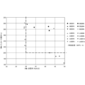
- Figure 1 is a diagram plotting the characteristics of Examples 1 to 6 and Comparative Examples 5 to 12, with the electrical conductivity (%IACS) at 500°C aging treatment taken on the X axis and the Vickers hardness (Hv) taken on the Y axis. be.
- %IACS electrical conductivity
- Hv Vickers hardness
- Figure 2 is a diagram plotting the characteristics of electrical conductivity (%IACS) or Vickers hardness (Hv) when the aging treatment temperature was changed from 400°C to 700°C in Examples 1 to 6. be.
- the temperature range of the aging treatment in Examples 1 to 6 is preferably 450 ° C. or higher and 550 ° C. or lower, preferably 550 ° C. if you want to increase the conductivity, and 500 ° C. if you want to increase the Vickers hardness.
- Copper alloy powder for additive manufacturing is manufactured by changing the content and content ratio of nickel and silicon and the content of other metal elements, and then copper is produced by additive manufacturing using the copper alloy powder for additive manufacturing. Alloy additively manufactured bodies were manufactured and their properties were measured.
- a copper alloy powder for additive manufacturing of a copper alloy containing nickel and silicon and other metal elements shown in Table 3 was produced by a gas atomization method.
- the obtained copper alloy powder for additive manufacturing was classified into a particle size of 10 ⁇ m or more and 45 ⁇ m or less for laser powder bed melting, and a particle size of 45 ⁇ m or more and 105 ⁇ m or less for electron beam powder bed melting. .
- the content of component elements in the obtained copper alloy powder for additive manufacturing was measured by ICP emission spectroscopy. Further, the apparent density (AD) (g/cm 3 ) of the obtained copper alloy powder for additive manufacturing was measured according to JIS Z 2504. Further, the flow rate (FR) (sec/50 g) of the obtained copper alloy powder for additive manufacturing was measured according to JIS Z 2502. Further, the 50% particle size (D50) ( ⁇ m) was measured by laser diffraction method (Microtrac MT3300: manufactured by Microtrac Bell Co., Ltd.).
- a shear test was conducted using a powder rheometer FT4 (manufactured by Freeman Technology), and the adhesion force (kPa) of the obtained copper alloy powder for additive manufacturing was measured.
- the squeezing property of the obtained copper alloy powder for additive manufacturing was measured by actually spreading the powder to be used for the modeling test on the modeling stage of a 3D additive manufacturing machine (powder sintering additive manufacturing/laser method or electron beam method). Evaluation was made by forming a layer.
- Table 3 shows the measurement results of each characteristic of the copper alloy powders for additive manufacturing of Examples 10 to 19.
- a laminate manufactured body for testing was produced using a 3D powder additive manufacturing machine (SLM Solutions GmbH, SLM280HL) equipped with a Yb fiber laser with a wavelength of 1064 nm. did.
- the additive manufacturing was performed under the following conditions: a layer thickness of 25 ⁇ m or more and 50 ⁇ m or less, a laser output of 300 W or more and 700 W or less, a scanning speed of 900 mm/sec or more and 1500 mm/sec or less, and an energy density of 150 J/mm 3 or more and 450 J/mm 3 or less.
- a laminate model to be tested was manufactured using a 3D powder additive manufacturing machine (ArcamAB, EBM A2X) equipped with an electron beam.
- the additive manufacturing was performed under the conditions that the layer thickness was 50 ⁇ m or more and 100 ⁇ m or less, the electron beam voltage was 60 kV, and the preheating temperature was 300° C. or more and 700° C. or less.
- a cylindrical additive-molded body having a diameter of 14 mm and a height of 10 mm was manufactured using a 3D powder additive manufacturing machine.
- the electrical conductivity (%IACS) of the copper alloy additive bodies of Examples 10 to 19 manufactured using a 3D powder additive manufacturing machine was measured using an eddy current conductivity meter (high performance eddy current conductivity meter Sigma Check: Nippon Matec) Co., Ltd.).
- the Vickers hardness (Hv) of the copper alloy laminate-molded body was measured using a microhardness tester (microhardness tester HMV-G21-DT: manufactured by Shimadzu Corporation).
- the prepared copper alloy laminate was subjected to aging treatment for 1 hour at temperatures set at 400°C, 500°C, 600°C, and 700°C in an inert atmosphere.
- the conductivity of the aged copper alloy laminate was measured using an eddy current conductivity meter.
- Vickers hardness was measured using a microhardness tester.
- Table 4 shows the evaluation results of various properties of the additively molded bodies of Examples 10 to 19 manufactured using the 3D powder additive manufacturing machine. In Table 4, the values of the properties surrounded by thick frames indicate values that satisfy the condition range as a copper alloy layered product.
- the content and ratio of nickel and silicon, and the properties of the copper alloy powder for additive manufacturing are within the required range, so that sufficient electrical conductivity (30% IACS or more) is achieved by the prescribed aging treatment. It was possible to fabricate a copper alloy laminate-molded body having both high strength and strength (Vickers hardness: 200 Hv or more).
- FIG. 3 is a graph plotting the characteristics of Examples 10 to 19, with the electrical conductivity (%IACS) at 500°C aging treatment taken on the X axis and the Vickers hardness (Hv) taken on the Y axis.
- Examples 10 and 11 which are copper alloy layered products containing nickel, silicon, and iron, are compared with Example 1, which is a copper alloy layered product that contains equivalent nickel and silicon, but does not contain iron.
- Example 1 which is a copper alloy layered product that contains equivalent nickel and silicon, but does not contain iron.
- Example 15 which is a copper alloy laminate-molded body containing nickel, silicon, and silver, has a higher Vickers laminate than Example 1, which is a copper alloy laminate-molded body that contains equivalent nickel and silicon but does not contain silver. Although the hardness is almost the same, the conductivity is improved. Furthermore, in Example 16, the Vickers hardness was improved while maintaining the same electrical conductivity.
- Example 17 which is a copper alloy laminate-molded body containing nickel, silicon, and magnesium, has higher conductivity than Example 2, which is a copper alloy laminate-molded body that contains equivalent nickel and silicon but does not contain magnesium. Vickers hardness has been improved while suppressing the decrease in hardness.
- Example 18 which is a copper alloy layered product containing nickel, silicon, magnesium, and manganese
- Example 1 which is a copper alloy layered product containing equivalent nickel and silicon, and containing neither magnesium nor manganese.
- the Vickers hardness after aging treatment at 500°C is significantly improved compared to the above.
- Example 19 which is a copper alloy layered product containing nickel, silicon, tin, and zinc
- Example 3 which is a copper alloy layered product containing equivalent nickel and silicon, and containing neither tin nor zinc. The Vickers hardness is improved regardless of the heat treatment conditions.
- FIG. 4 is a diagram plotting the characteristics of electrical conductivity (%IACS) or Vickers hardness (Hv) when the aging treatment temperature was changed from 400°C to 700°C in Examples 10 to 19. be.
- the temperature range of the aging treatment in Examples 10 to 19 is preferably 450 ° C. or higher and 550 ° C. or lower, preferably 550 ° C. if you want to increase the electrical conductivity, and 500 ° C. if you want to increase the Vickers hardness.
- Arc melting was performed using the same copper alloy powder for additive manufacturing as in Examples 1 to 5, 10 to 13, and 15 to 19 to produce arc melted materials.
- the arc melted lumber was produced as shown below.
- the copper alloy powders for additive manufacturing of Examples 1 to 5, 10 to 13, and 15 to 19 were press-molded to produce green compacts.
- the produced compact was arc melted in an argon atmosphere using a vacuum arc melting furnace manufactured by Nissin Giken Co., Ltd. to produce an arc melted material.
- These arc-melted materials were designated as Comparative Examples 21 to 34.
- Example 6 has the same composition as Example 1
- Example 14 has the same composition as Example 10
- the arc-melted material using the same copper alloy powder for additive manufacturing as Examples 6 and 14 is Not created.
- the electrical conductivity (%IACS) of the arc melted materials of Comparative Examples 21 to 34 produced by arc melting was measured using an eddy current conductivity meter (high performance eddy current conductivity meter Sigma Check: manufactured by Nippon Matek Co., Ltd.).
- Vickers hardness (Hv) was measured using a microhardness tester (microhardness tester HMV-G21-DT: manufactured by Shimadzu Corporation).
- the produced arc melted materials were subjected to aging treatment for 1 hour at temperatures set at 400, 500, 600, and 700°C in an inert atmosphere.
- the electrical conductivity of the aged arc melted lumber was measured using an eddy current conductivity meter.
- Vickers hardness was measured using a microhardness tester.
- Table 5 shows the evaluation results of various properties of the arc-melted materials of Comparative Examples 21 to 34.
- the underlined property values indicate values that do not satisfy the condition range for a copper alloy shaped body even after aging treatment at 500°C.
- the rolled arc-melted material was aged in an inert atmosphere at temperatures of 400, 500, 600, and 700°C for 1 hour.
- the electrical conductivity of the arc melted sawn material that had been subjected to aging treatment and rolling processing was measured using an eddy current conductivity meter.
- Vickers hardness was measured using a microhardness tester.
- Table 6 shows the evaluation results of various properties of the arc-melted materials subjected to rolling processing in Comparative Examples 41 to 54.
- the underlined property values indicate values that do not satisfy the condition range for a copper alloy shaped body even after aging treatment at 500°C.
- Figure 5 shows the characteristics of the copper alloy laminate manufactured bodies of Examples 1 to 6 and 10 to 19 after aging treatment at 500°C, the arc melted materials of Comparative Examples 21 to 34, and the rolling processing of Comparative Examples 41 to 54. It is a diagram plotting the characteristics of arc-molten material with electrical conductivity (%IACS) on the X-axis and Vickers hardness (Hv) on the Y-axis.
- %IACS electrical conductivity
- Hv Vickers hardness
Abstract
The present invention makes it possible to manufacture an additively-manufactured copper alloy article having high strength by efficiently producing a Corson alloy from nickel and silicon. This copper alloy powder for additive manufacturing is used to manufacture an additively-manufactured article by additive manufacturing, the copper alloy powder for additive manufacturing containing nickel and silicon with the remainder made up by copper and unavoidable impurities, the value obtained by dividing the nickel content (wt%) by the silicon content (wt%) being 3.3 to 7.2. This copper alloy additively-manufactured article is additively manufactured by an additive manufacturing device, the copper alloy additively-manufactured article containing 1.5 wt% to 6.0 wt% of nickel and 0.35 wt% to 1.5 wt% of silicon with the remainder made up by copper and unavoidable impurities, and being such that the value obtained by dividing the nickel content (wt%) by the silicon content (wt%) is 3.3 to 7.2.
Description
本発明は、積層造形用銅合金粉末、銅合金積層造形体および銅合金積層造形体の製造方法に関する。
The present invention relates to a copper alloy powder for layered manufacturing, a copper alloy layered object, and a method for producing a copper alloy layered object.
上記技術分野において、特許文献1には、銅にニッケル元素およびシリコン元素を含有する積層造形用の銅基合金粉末が開示されている。
In the above technical field, Patent Document 1 discloses a copper-based alloy powder for additive manufacturing that contains nickel and silicon elements in copper.
しかしながら、上記文献に記載の技術では、ニッケルとシリコンとによるコルソン合金を効率的に生成しないので、高強度の銅合金積層造形体を製造することができなかった。
However, the technique described in the above-mentioned document does not efficiently produce a Corson alloy of nickel and silicon, and therefore cannot produce a high-strength copper alloy laminate-molded body.
本発明の目的は、上述の課題を解決する技術を提供することにある。
An object of the present invention is to provide a technology that solves the above problems.
上記目的を達成するため、本発明に係る積層造形用銅合金粉末は、
積層造形法により積層造形体を造形するために用いられる積層造形用銅合金粉末であって、
ニッケルおよびシリコンを含有し、残部が銅および不可避的不純物からなり、
前記ニッケルの含有量(重量%)を前記シリコンの含有量(重量%)で除した値が3.3以上7.2以下である。 In order to achieve the above object, the copper alloy powder for additive manufacturing according to the present invention,
A copper alloy powder for additive manufacturing used for forming a additively manufactured object by an additive manufacturing method,
Contains nickel and silicon, with the remainder consisting of copper and unavoidable impurities,
A value obtained by dividing the nickel content (wt%) by the silicon content (wt%) is 3.3 or more and 7.2 or less.
上記目的を達成するため、本発明に係る銅合金積層造形体は、
上記の積層造形用銅合金粉末を用いて、積層造形装置により積層造形された銅合金積層造形体であって、
ニッケルの含有量(重量%)をシリコンの含有量(重量%)で除した値が3.3以上7.2以下である。 In order to achieve the above object, the copper alloy layered product according to the present invention has the following features:
A copper alloy additively manufactured body produced by additively manufacturing using an additively manufacturing apparatus using the above-mentioned copper alloy powder for additively manufacturing,
The value obtained by dividing the nickel content (wt%) by the silicon content (wt%) is 3.3 or more and 7.2 or less.
上記目的を達成するため、本発明に係る銅合金積層造形体の製造方法は、
上記の積層造形用銅合金粉末を用いて、積層造形装置により銅合金積層造形体を積層造形する積層造形工程と、
前記銅合金積層造形体を、450℃以上550℃以下で保持する時効処理工程と、
を含む。 In order to achieve the above object, the method for manufacturing a copper alloy layered product according to the present invention includes:
An additive manufacturing step of additively manufacturing a copper alloy additive-molded body using an additive manufacturing device using the copper alloy powder for additive manufacturing;
an aging treatment step of holding the copper alloy layered product at a temperature of 450° C. or higher and 550° C. or lower;
including.
本発明によれば、ニッケルとシリコンとによるコルソン合金を効率的に生成することで高強度の銅合金積層造形体を製造することができる。
According to the present invention, a high-strength copper alloy laminate can be manufactured by efficiently producing a Corson alloy of nickel and silicon.
以下に、図面を参照して、本発明の実施の形態について例示的に詳しく説明する。ただし、以下の実施の形態に記載されている構成要素は単なる例示であり、本発明の技術範囲をそれらのみに限定する趣旨のものではない。
Hereinafter, embodiments of the present invention will be described in detail by way of example with reference to the drawings. However, the components described in the following embodiments are merely examples, and the technical scope of the present invention is not intended to be limited thereto.
[第1実施形態]
本実施形態においては、ニッケルおよびシリコンを含有し、残部が銅および不可避的不純物からなる積層造形用銅合金粉末と、その積層造形用銅合金粉末を用いて積層造形された銅合金積層造形体について説明する。 [First embodiment]
In this embodiment, we will discuss a copper alloy powder for additive manufacturing containing nickel and silicon, with the remainder being copper and unavoidable impurities, and a copper alloy additive manufacturing object that is additively manufactured using the copper alloy powder for additive manufacturing. explain.
<積層造形用銅合金粉末の製造>
本実施形態の積層造形用銅合金粉末の製造方法は特に限定されないが、ガスアトマイズ法、水アトマイズ法、遠心アトマイズ法、プラズマアトマイズ法、プラズマ回転電極法等のように、粉末粒子が溶融状態から急冷凝固される方式が好ましい。量産性の点からは、ガスアトマイズ法が特に好ましい。製造した粉末は、公知の分級方法によって、所定の分級条件にて分級し、適切な粒度の積層造形用銅合金粉末に調整することができる。分級を実施するための分級装置としては、気流分級機を好適に用いることができる。 <Manufacture of copper alloy powder for additive manufacturing>
The manufacturing method of the copper alloy powder for additive manufacturing of this embodiment is not particularly limited, but there are methods such as gas atomization method, water atomization method, centrifugal atomization method, plasma atomization method, plasma rotating electrode method, etc., in which powder particles are rapidly cooled from a molten state. A solidified method is preferred. From the point of view of mass production, gas atomization is particularly preferred. The manufactured powder can be classified by a known classification method under predetermined classification conditions, and can be adjusted to a copper alloy powder for additive manufacturing with an appropriate particle size. As a classification device for carrying out the classification, an air classifier can be suitably used.
(本実施形態の積層造形用銅合金粉末が含有する金属の条件)
析出強化型銅合金であるコルソン合金では、基質である銅に過飽和固溶したニッケルおよびシリコンが時効処理によってニッケル-シリコン金属間化合物を生成して析出し、銅合金の強度が向上する。 (Conditions for the metal contained in the copper alloy powder for additive manufacturing of this embodiment)
In the Corson alloy, which is a precipitation-strengthened copper alloy, nickel and silicon, which are supersaturated solid solutions in the copper substrate, are aged to form a nickel-silicon intermetallic compound and precipitate, improving the strength of the copper alloy.
高い機械的強度を有する銅合金積層造形体を得るためには、ニッケルの含有量は1.5重量%以上が好ましい。1.5重量%未満の場合には、時効処理において析出量が不十分となり、強度向上の効果を十分に得られない。なお、コルソン合金におけるニッケル-シリコン金属間化合物の1つであるNi2Siの固溶限は、ニッケルが約4.2重量%、シリコンが1.0重量%と言われている。しかし、粉末製造方法としてアトマイズ法など金属を溶解して急速凝固させる製法を用いた場合、固溶限以上のニッケル-シリコン金属間化合物を析出させずに銅基質中に含ませることができる。
In order to obtain a copper alloy layered product with high mechanical strength, the nickel content is preferably 1.5% by weight or more. If it is less than 1.5% by weight, the amount of precipitation during aging treatment will be insufficient, and the effect of improving strength will not be sufficiently obtained. Note that the solid solubility limit of Ni2Si, which is one of the nickel-silicon intermetallic compounds in the Corson alloy, is said to be approximately 4.2% by weight for nickel and 1.0% by weight for silicon. However, when a powder manufacturing method such as an atomization method is used in which the metal is melted and rapidly solidified, the nickel-silicon intermetallic compound exceeding the solid solubility limit can be contained in the copper matrix without precipitation.
また、粉末床溶融法の積層造形法を用いた場合、その工程上、レーザもしくは電子ビームによる溶融と急速凝固が行われるため、固溶限以上のニッケル-シリコン金属間化合物を析出させることなく造形体を作製することができる。ただし、ニッケルの含有量が6.0重量%を超えて含有した場合、さらなる機械的強度向上の効果が得られるが、導電率の大幅な低下を招いてしまう。そのため、ニッケルの含有量は6.0重量%以下が好ましい。
In addition, when using the additive manufacturing method using the powder bed melting method, the process involves melting and rapid solidification using a laser or electron beam, so it is possible to build without precipitating nickel-silicon intermetallic compounds exceeding the solid solubility limit. body can be created. However, if the nickel content exceeds 6.0% by weight, the effect of further improving mechanical strength can be obtained, but this results in a significant decrease in electrical conductivity. Therefore, the nickel content is preferably 6.0% by weight or less.
シリコンはニッケルと共にニッケル-シリコン金属間化合物を生成して析出し、銅合金の強度向上に寄与する主要な元素である。その含有量が0.35重量%未満の場合には、時効処理において析出量が不十分となり、強度向上の効果を十分に得られない。また、1.5重量%よりも多くなると、導電率が大幅に低下し、また粗大な析出物が生成し強度の低下をもたらすため、本実施形態の範囲にあることが好ましい。
Silicon is a major element that forms and precipitates a nickel-silicon intermetallic compound together with nickel, contributing to improving the strength of copper alloys. If the content is less than 0.35% by weight, the amount of precipitation during aging treatment will be insufficient, and the effect of improving strength will not be sufficiently obtained. Further, if the amount exceeds 1.5% by weight, the conductivity will be significantly lowered and coarse precipitates will be formed, resulting in a decrease in strength, so it is preferably within the range of this embodiment.
ニッケルおよびシリコンは、ニッケル-シリコン金属間化合物を生成して、導電率および強度の向上に寄与する主要な元素である。ただし、導電率および強度の両特性を向上させるためには、ニッケルおよびシリコンのそれぞれの含有量の範囲内において、ニッケル-シリコン金属間化合物を形成するのに効率的な比率で含有することが必要である。その比率は、ニッケルの含有量(重量%)をシリコンの含有量(重量%)で除した値が3.3以上7.2以下の範囲内となることが好ましい。この比率が7.2を超えて、ニッケルがシリコンに対して過剰に含まれた場合、過剰分のニッケルが銅基質に固溶するため導電率が大幅に低下してしまう。一方、比率が3.3未満で、シリコンがニッケルに対して過剰に含まれた場合は、過剰分のシリコンが銅基質に固溶するため導電率が大幅に低下してしまう。
Nickel and silicon are the main elements that form nickel-silicon intermetallic compounds and contribute to improving electrical conductivity and strength. However, in order to improve both electrical conductivity and strength, it is necessary to contain nickel and silicon in an efficient ratio within their respective content ranges to form a nickel-silicon intermetallic compound. It is. As for the ratio, the value obtained by dividing the nickel content (wt%) by the silicon content (wt%) is preferably in the range of 3.3 or more and 7.2 or less. If this ratio exceeds 7.2 and nickel is contained in excess of silicon, the excess nickel will be dissolved in the copper matrix, resulting in a significant decrease in electrical conductivity. On the other hand, if the ratio is less than 3.3 and silicon is contained in excess of nickel, the excess silicon will dissolve in the copper matrix, resulting in a significant decrease in electrical conductivity.
(本実施形態の積層造形用銅合金粉末が有する物理的特性の条件)
積層造形用として用いられる粉末には、ホッパーから造形ステージ上への供給工程や、一定の厚みで均一に敷き詰められた粉末層を形成する工程、溶融凝固の工程など、積層造形の各プロセスに適合していることが要求される。そのため、以下の条件が必要とされる。その条件とは、適切な範囲内に調整された粒径、適切な範囲内の見掛密度、供給ホッパーからの供給が可能であり、かつ、適切な粉末層を形成可能とする粉末の流動性である。 (Conditions for physical properties of the copper alloy powder for additive manufacturing of this embodiment)
The powder used for additive manufacturing is compatible with each process of additive manufacturing, such as the feeding process from a hopper onto the modeling stage, the process of forming a uniformly spread powder layer with a constant thickness, and the process of melting and solidification. are required to do so. Therefore, the following conditions are required. The conditions are: particle size adjusted within an appropriate range, apparent density within an appropriate range, and powder fluidity that allows it to be fed from the supply hopper and form an appropriate powder layer. It is.
積層造形用銅合金粉末の50%粒径は、レーザ回折法で測定したときの、粒子径分布の50%粒径のことであり、3μm以上200μm以下の範囲に含まれることが好ましい。50%粒径が3μm未満の場合には、粉末の流動性がなく、レーザ方式粉末床溶融法の積層造形装置においても粉末層を形成できない。また、50%粒径が3μm未満の粉末にレーザを照射した場合、粉末および粉末の溶融によって生じた液滴が飛散するため、積層造形には不適である。レーザ方式粉末床溶融法で積層造形する場合は50%粒径が100μmより大きい場合、電子ビーム方式粉末床溶融法で積層造形する場合は50%粒径が200μmより大きい場合は、粉末層の表面が荒れて造形に適切な粉末層を形成できない。また、電子ビーム照射時に粉末層に生じたメルトプールが直下の凝固層にまで達せず、不十分な溶融凝固となるため、積層造形には不適である。
The 50% particle size of the copper alloy powder for additive manufacturing refers to the 50% particle size of the particle size distribution when measured by laser diffraction, and is preferably in the range of 3 μm or more and 200 μm or less. When the 50% particle size is less than 3 μm, the powder has no fluidity, and a powder layer cannot be formed even in an additive manufacturing apparatus using a laser powder bed melting method. Furthermore, when laser is irradiated to powder with a 50% particle size of less than 3 μm, the powder and droplets generated by melting the powder scatter, making it unsuitable for additive manufacturing. If the 50% particle size is larger than 100 μm when additive manufacturing is performed using laser powder bed melting method, and when the 50% particle size is larger than 200 μm when additive manufacturing is performed using electron beam powder bed melting method, the surface of the powder layer The powder layer becomes rough and cannot form an appropriate powder layer for modeling. Furthermore, the melt pool generated in the powder layer during electron beam irradiation does not reach the solidified layer immediately below, resulting in insufficient melting and solidification, making it unsuitable for additive manufacturing.
レーザ方式粉末床溶融法においては、50%粒径は3μm以上100μm以下であることが好ましく、5μm以上75μm以下であることがより好ましく、さらに10μm以上45μm以下であることがより好ましい。電子ビーム方式粉末床溶融法においては、50%粒径は10μm以上200μm以下であることが好ましく、25μm以上150μm以下であることがより好ましく、さらに45μm以上105μm以下であることがより好ましい。
In the laser powder bed melting method, the 50% particle size is preferably 3 μm or more and 100 μm or less, more preferably 5 μm or more and 75 μm or less, and even more preferably 10 μm or more and 45 μm or less. In the electron beam powder bed melting method, the 50% particle size is preferably 10 μm or more and 200 μm or less, more preferably 25 μm or more and 150 μm or less, and even more preferably 45 μm or more and 105 μm or less.
積層造形装置による積層造形が可能な銅合金粉末としては、ISO 3923-1に準ずるJIS Z 2504の測定法で測定したときの積層造形用銅合金粉末の見掛密度(AD:Apparent Density)が3.0g/cm3以上であることが必要とされる。見掛密度が3.0g/cm3未満の場合、スキージングによって敷き詰められた粉末層の粉末充填率が低下して適切な粉末層を形成できない。また、粉末の充填率が低下することで、造形体に空孔が生じて造形体の密度が低下してしまう。高密度の積層造形体を得るためには、積層造形用銅合金粉末の見掛密度は、3.5g/cm3以上であることがより好ましい。
Copper alloy powder that can be additively manufactured using an additive manufacturing device has an apparent density (AD: Apparent Density) of 3 when measured using the JIS Z 2504 measurement method based on ISO 3923-1. .0g/cm3 or more is required. When the apparent density is less than 3.0 g/cm 3 , the powder filling rate of the powder layer spread by squeegeeing decreases, making it impossible to form an appropriate powder layer. In addition, as the powder filling rate decreases, pores are generated in the shaped body, resulting in a decrease in the density of the shaped body. In order to obtain a high-density layered product, the apparent density of the copper alloy powder for layered manufacturing is more preferably 3.5 g/cm 3 or more.
積層造形法においては、流動性が特に重要とされる粉末特性である。特に粉末床溶融法では、供給ホッパーからの粉末供給および、リコータからの粉末供給、造形ステージ上での粉末層の形成と、造形体の品質にも直結する最も重要な粉末特性である。粉末床溶融法では、造形ステージ上に粉末を一定の厚みで均一に敷き詰める必要がある。この粉末を敷き詰める工程はスキージングと呼ばれており、粉末の敷き詰め性の良し悪しをスキージング性と呼ぶ。積層造形法にて用いられる粉末には十分なスキージング性が必要であり、そのためには粉末に適切な流動性が必要とされる。
In additive manufacturing, fluidity is a particularly important powder property. Particularly in the powder bed melting method, the most important powder characteristics are the powder supply from the supply hopper, the powder supply from the recoater, and the formation of a powder layer on the modeling stage, which are directly linked to the quality of the shaped object. In the powder bed melting method, it is necessary to uniformly spread the powder on the modeling stage with a certain thickness. This process of spreading the powder is called squeezing, and the quality of the spreading of the powder is called squeegeeability. The powder used in additive manufacturing requires sufficient squeegeeability, and for this purpose, the powder needs to have appropriate fluidity.
金属粉末の流動性を測定する指標として、ISO 4490に準ずるJIS Z 2502「金属粉-流動度測定方法」の定める流動度(FR:Flow Rate)が用いられる。しかしながら、レーザ方式粉末床溶融法向けとして主に使用される50%粒径が50μm以下の微粉では、粉末が測定容器から流出せず測定不可となり、流動性を評価できない場合がある。そのため、微粉の流動性を評価する指標としては、日本粉体工業技術協会規格(SAP15-13:2013)「粉体の一面せん断試験方法」にて規定されている、粉体の一面せん断試験方法(以下、せん断試験)により得られる粉末の付着力を使用することが有効である。付着力は、せん断試験において、垂直方向に圧密して形成させた粉体層を垂直方向に加圧した状態で、水平方向に横滑りさせた時に生じるせん断応力を測定することで、得られた粉体層の破壊包絡線から求めることができる。
As an index for measuring the fluidity of metal powder, the flow rate (FR) defined by JIS Z 2502 "Metal powder - Flow rate measurement method" based on ISO 4490 is used. However, in the case of fine powder with a 50% particle size of 50 μm or less, which is mainly used for laser-based powder bed melting, the powder does not flow out of the measurement container and cannot be measured, making it impossible to evaluate fluidity. Therefore, as an index for evaluating the fluidity of fine powder, the one-sided shear test method for powder specified in the Japan Powder Industry Technology Association standard (SAP15-13: 2013) "One-plane shear test method for powder" is recommended. It is effective to use the adhesion force of powder obtained by (hereinafter referred to as a shear test). Adhesion strength is measured in a shear test by measuring the shear stress that occurs when a powder layer formed by compacting the powder in the vertical direction is slid horizontally under pressure in the vertical direction. It can be determined from the fracture envelope of the body layer.
せん断試験は、例えば、フリーマンテクノロジー社製のパウダーレオメータFT4を用いることで測定することができる。積層造形用銅合金粉末については、その付着力が0.600kPa以下であれば、均一な粉末層を敷き詰めることができる十分な流動性を有し、スキージング性が良好であると判断することができる。これによって、高密度で均質な積層造形体が得られる。付着力が0.600kPaより大きい場合は、積層造形用銅合金粉末の流動性が十分ではなく、スキージング性は不良となって適切な粉体層を形成することができない。よって、積層造形用銅合金粉末においては、せん断試験によって得られた破壊包絡線から求めた銅合金粉末の付着力が、0.600kPa以下であることが望ましい。
The shear test can be measured using, for example, a powder rheometer FT4 manufactured by Freeman Technology. Regarding copper alloy powder for additive manufacturing, if its adhesive force is 0.600 kPa or less, it can be judged that it has sufficient fluidity to spread a uniform powder layer and has good squeegeeability. can. As a result, a high-density and homogeneous laminate-molded body can be obtained. When the adhesion force is greater than 0.600 kPa, the fluidity of the copper alloy powder for additive manufacturing is insufficient, the squeezing property is poor, and an appropriate powder layer cannot be formed. Therefore, in the copper alloy powder for additive manufacturing, it is desirable that the adhesion force of the copper alloy powder determined from the fracture envelope obtained by the shear test is 0.600 kPa or less.
<本実施形態の積層造形用銅合金粉末を用いた銅合金積層造形体の製造>
銅合金積層造形体の製造方法としては、種々公知の金属積層造形技術を用いることができる。例えば粉末床溶融法では、金属粉末を造形ステージにブレードあるいはローラーなどでならして敷き詰めて粉末層を形成し、形成した粉末層の所定位置にレーザあるいは電子ビームを照射して金属粉末を焼結・溶融させる工程を繰り返しながら積層造形体の作製を行う。金属積層造形の造形プロセスにおいては、高品質な造形体を得るために非常に多数のプロセスパラメータを制御する必要がある。 <Manufacture of a copper alloy layered object using the copper alloy powder for layered manufacturing of this embodiment>
Various known metal additive manufacturing techniques can be used as a method for manufacturing the copper alloy additive manufacturing body. For example, in the powder bed fusion method, metal powder is spread on a modeling stage using a blade or roller to form a powder layer, and a laser or electron beam is irradiated at a predetermined position on the formed powder layer to sinter the metal powder.・Produce a layered object by repeating the melting process. In the metal additive manufacturing process, it is necessary to control a large number of process parameters in order to obtain a high-quality shaped object.
レーザ方式粉末床溶融法においては、レーザ出力やレーザの走査速度など多数の走査条件が存在する。そこで、最適な走査条件を設定するにあたり、主要なパラメータを総括した指標であるエネルギー密度を用いて、主要パラメータの調整を行う。エネルギー密度E(J/mm3)は、レーザの出力をP(W)、レーザの走査速度をv(mm/s)、レーザ走査ピッチをs(mm)、粉末層の厚みをt(mm)とすると、E=P/(v×s×t)により決定される。レーザ方式粉末床溶融法においては、エネルギー密度は150J/mm3以上450J/mm3以下が好ましい。エネルギー密度が150J/mm3未満の場合、粉末層に未溶融や融合不良が生じ、造形体に空隙などの欠陥が生じてしまう。エネルギー密度が450J/mm3を超える場合、スパッタリングが生じて粉末層の表面が不安定となり、造形体に空隙などの欠陥が生じてしまう。
In the laser powder bed melting method, there are many scanning conditions such as laser output and laser scanning speed. Therefore, in setting the optimal scanning conditions, the main parameters are adjusted using energy density, which is an index that summarizes the main parameters. The energy density E (J/mm 3 ) is determined by the laser output in P (W), the laser scanning speed in v (mm/s), the laser scanning pitch in s (mm), and the powder layer thickness in t (mm). Then, E=P/(v×s×t) is determined. In the laser powder bed melting method, the energy density is preferably 150 J/mm 3 or more and 450 J/mm 3 or less. If the energy density is less than 150 J/mm 3 , the powder layer will be unfused or poorly fused, resulting in defects such as voids in the shaped body. When the energy density exceeds 450 J/mm 3 , sputtering occurs and the surface of the powder layer becomes unstable, resulting in defects such as voids in the shaped body.
一方、電子ビーム方式粉末床溶融法においては、電子ビームを粉末層に照射した際に、粉末層に負電荷が蓄積されてチャージアップすると、粉末が霧状に舞い上がるスモーク現象が引き起こされてしまい、溶融不良につながってしまう。そのため、チャージアップを防ぐために粉末層を予備加熱して仮焼結させる予備工程が必要とされる。ただし、予備加熱温度が高過ぎる場合、焼結が進行してネッキングを引き起こし、造形後に積層造形体内部から残留した粉末を除去するのが困難となる。このため、積層造形用銅合金粉末においては、予備加熱温度は300℃以上800℃以下に設定するのが好ましい。
On the other hand, in the electron beam powder bed melting method, when the powder layer is irradiated with an electron beam, negative charges accumulate in the powder layer and charge up, causing a smoke phenomenon in which the powder flies up in the form of mist. This will lead to poor melting. Therefore, in order to prevent charge-up, a preliminary step is required in which the powder layer is preheated and temporarily sintered. However, if the preheating temperature is too high, sintering progresses and necking occurs, making it difficult to remove residual powder from inside the layered product after modeling. For this reason, in the copper alloy powder for additive manufacturing, the preheating temperature is preferably set at 300°C or more and 800°C or less.
なお、ここでは粉末床溶融法による金属積層造形技術を例示したが、本実施形態の積層造形用銅合金粉末を用いて積層造形体を製造する一般的な積層造形方法としては、これに限定されるものではなく、例えば、指向性エネルギー堆積法による積層造形方法を採用してもよい。
Although the metal additive manufacturing technology using the powder bed melting method is illustrated here, the general additive manufacturing method for producing a additively manufactured object using the copper alloy powder for additive manufacturing of this embodiment is limited to this. For example, an additive manufacturing method using a directed energy deposition method may be adopted.
(銅合金積層造形体に対する時効処理)
銅合金積層造形体に時効処理を施すことで、過飽和に固溶したニッケルおよびシリコンが析出し、積層造形体の強度が向上し導電率が向上する。そのため時効処理工程は、本実施形態の高強度かつ高導電率の特性を得るためには必須の工程である。時効処理は、積層造形体を所定の温度に加熱し、所定の時間保持することで実施できる。時効処理は還元性雰囲気もしくは不活性ガス中、真空で行うことが好ましい。 (Aging treatment for copper alloy layered object)
By subjecting the copper alloy laminate to an aging treatment, supersaturated solid solution nickel and silicon precipitate, improving the strength and electrical conductivity of the laminate. Therefore, the aging treatment step is an essential step in order to obtain the high strength and high conductivity properties of this embodiment. The aging treatment can be carried out by heating the laminate to a predetermined temperature and holding it for a predetermined time. The aging treatment is preferably carried out in a reducing atmosphere or inert gas in a vacuum.
時効処理の効果は、時効処理温度と時効処理時間の組み合わせで決まるので、目的とする特性と効率との兼ね合いで、適切な条件を設定することが重要である。時効処理温度は450℃以上550℃以下が好ましい。より好ましくは、450℃以上500℃以下である。機械的強度を特に向上させたい場合には500℃とすることが好ましい。特に高い導電率を得たい場合には550℃にすることもできる。時効処理時間は、時効処理温度が450℃以上の場合には、0.5時間以上3時間以下に設定するのが好ましい。
The effect of aging treatment is determined by the combination of aging treatment temperature and aging treatment time, so it is important to set appropriate conditions in balance with the desired characteristics and efficiency. The aging treatment temperature is preferably 450°C or more and 550°C or less. More preferably, the temperature is 450°C or higher and 500°C or lower. When it is desired to particularly improve mechanical strength, the temperature is preferably 500°C. If particularly high conductivity is desired, the temperature can be set at 550°C. When the aging treatment temperature is 450° C. or higher, the aging treatment time is preferably set to 0.5 hours or more and 3 hours or less.
時効処理時間が設定時間未満の場合には、ニッケルおよびシリコンの析出が不十分となる。また、時効処理時間が設定時間を超える場合には、過時効となって析出したニッケル-シリコン金属間化合物が粗大化し、硬度の低下を招く。時効処理温度が450℃未満の場合には、時効の効果が得られるまでに長時間を要するので実用的ではない。また、時効処理温度が550℃を超える場合には、過時効となり、ニッケル-シリコン金属間化合物の析出相が粗大化して強度が低下してしまう。
If the aging treatment time is less than the set time, the precipitation of nickel and silicon will be insufficient. Furthermore, if the aging treatment time exceeds the set time, the nickel-silicon intermetallic compound precipitated due to overaging becomes coarse, resulting in a decrease in hardness. If the aging treatment temperature is less than 450° C., it is not practical because it takes a long time to obtain the aging effect. Further, if the aging treatment temperature exceeds 550° C., over-aging occurs, and the precipitated phase of the nickel-silicon intermetallic compound becomes coarse, resulting in a decrease in strength.
本実施形態の積層造形用銅合金粉末を用いて積層造形した銅合金積層造形体においては、積層造形法の特徴である急速溶融凝固プロセスにより導入される熱歪みによってニッケル-シリコン金属間化合物が析出しやすくなる。そのため、時効処理温度450℃以上550℃以下で1時間程度の時効処理時間でも十分に導電率および機械的強度を向上させることが可能である。
In the copper alloy additively manufactured body that is additively manufactured using the copper alloy powder for additive manufacturing of this embodiment, nickel-silicon intermetallic compounds are precipitated due to thermal strain introduced by the rapid melting and solidification process that is a feature of additive manufacturing. It becomes easier to do. Therefore, it is possible to sufficiently improve the electrical conductivity and mechanical strength even with an aging treatment temperature of 450° C. or more and 550° C. or less and an aging treatment time of about 1 hour.
本実施形態の銅合金積層造形体のビッカース硬さは、JIS Z 2244:ビッカース硬さ試験-試験方法に準拠した方法により測定される。ビッカース硬さは例えば、株式会社島津製作所製の微小硬さ試験機HMV-G21-DTなどにより測定することができる。
The Vickers hardness of the copper alloy laminate-molded article of this embodiment is measured by a method based on JIS Z 2244: Vickers hardness test-test method. Vickers hardness can be measured using, for example, a microhardness tester HMV-G21-DT manufactured by Shimadzu Corporation.
また、本実施形態の銅合金積層造形体は、30%IACS以上の導電率を有する。導電率は、例えば渦流式導電率計などによって測定することができる。渦流式導電率計としては、例えば、日本マテック株式会社製の高性能渦流式導電率計シグマチェックなどが挙げられる。なお、IACS(International Annealed Copper Standard)とは、導電率の基準として、国際的に採択された焼鈍標準軟銅(体積抵抗率:1.7241×10⁻²μΩm)の導電率を、100%IACSとして規定されたものである。導電率は、時効処理によって調整することができ、所望するビッカース硬さとの兼ね合いによって適宜調整することが好ましい。導電率は35%IACS以上が好ましく、より好ましくは40%IACS以上である。
Moreover, the copper alloy laminate-molded article of this embodiment has an electrical conductivity of 30% IACS or more. The conductivity can be measured using, for example, an eddy current conductivity meter. Examples of the eddy current conductivity meter include the high performance eddy current conductivity meter Sigma Check manufactured by Nippon Matek Co., Ltd. In addition, IACS (International Annealed Copper Standard) refers to the electrical conductivity of internationally adopted annealed standard annealed copper (volume resistivity: 1.7241 x 10 -2 μΩm) as 100% IACS. It is prescribed. The electrical conductivity can be adjusted by aging treatment, and is preferably adjusted appropriately depending on the desired Vickers hardness. The conductivity is preferably 35% IACS or more, more preferably 40% IACS or more.
なお、金属においては、導電率と熱伝導率はほぼ比例関係にあることが、ウィーデマン・フランツの法則として知られている。よって、本実施形態の積層造形用銅合金粉末を用いて、積層造形装置により積層造形された銅合金積層造形体は、高い導電率を有することから、高熱伝導率を有する銅合金積層造形体としても使用可能である。
It is known as the Wiedemann-Franz law that in metals, electrical conductivity and thermal conductivity are almost proportional. Therefore, since the copper alloy additively manufactured body produced by additive manufacturing using the additively manufactured copper alloy powder of the present embodiment by the additive manufacturing apparatus has high electrical conductivity, it can be used as a copper alloy additively manufactured body having high thermal conductivity. is also available.
[第2実施形態]
本実施形態においては、ニッケルおよびシリコンと、他の金属元素、例えば鉄、銀、マグネシウム、マンガン、錫、および亜鉛から選択される1種または2種以上を含有し、残部が銅および不可避的不純物からなる積層造形用銅合金粉末と、その積層造形用銅合金粉末を用いて積層造形した銅合金積層造形体について説明する。 [Second embodiment]
In this embodiment, it contains nickel and silicon, and one or more selected from other metal elements such as iron, silver, magnesium, manganese, tin, and zinc, with the remainder being copper and unavoidable impurities. A copper alloy powder for additive manufacturing consisting of the following will be described, and a copper alloy additive-molded body produced by additive manufacturing using the copper alloy powder for additive manufacturing.
本実施形態の積層造形用銅合金粉末には、ニッケルおよびシリコンの含有に加えて、必要に応じて鉄、銀、マグネシウム、マンガン、錫および亜鉛から選択される1種または2種以上の元素を含有させることができる。これら金属元素の含有の効果について以下に説明する。
In addition to containing nickel and silicon, the copper alloy powder for additive manufacturing of this embodiment may contain one or more elements selected from iron, silver, magnesium, manganese, tin, and zinc as necessary. It can be included. The effects of containing these metal elements will be explained below.
・鉄の含有は、本実施形態の銅合金積層造形体の組織を微細化して強度を向上させる効果を有する。また、シリコンと化合することによって鉄-シリコン化合物を形成する。そのため、導電率を大きく落とさずに機械的特性、耐熱性を向上させることができる。鉄は0.01重量%以上1.00重量%以下の範囲に調整することが好ましく、0.05重量%以上0.30重量%以下の範囲に調整することがより好ましい。
- Containing iron has the effect of refining the structure of the copper alloy layered product of this embodiment and improving its strength. Further, by combining with silicon, an iron-silicon compound is formed. Therefore, mechanical properties and heat resistance can be improved without significantly reducing conductivity. Iron is preferably adjusted to a range of 0.01% to 1.00% by weight, more preferably 0.05% to 0.30% by weight.
・銀の含有は、本実施形態の銅合金積層造形体の導電率を高める効果および、固溶強化によって強度を高める効果があると考えられる。また、ニッケルの化学ポテンシャルを上昇させ、元素同士の反発相互作用を高めてニッケル-シリコン金属間化合物の析出を促す効果がある。銀の含有量が1.0重量%を超える場合には、銀の比率が高まるが、銀を増やしても特性上大きな効果は得られず、高価な銀を過剰に含有することでコストの増加を招く。そのため、銀は0.01重量%以上1.00重量%以下の範囲に調整することが好ましく、0.05重量%以上0.30重量%以下の範囲に調整することがより好ましい。
- It is thought that the inclusion of silver has the effect of increasing the electrical conductivity of the copper alloy laminate manufactured body of this embodiment and the effect of increasing the strength by solid solution strengthening. It also has the effect of increasing the chemical potential of nickel, increasing the repulsive interaction between elements, and promoting the precipitation of nickel-silicon intermetallic compounds. When the silver content exceeds 1.0% by weight, the ratio of silver increases, but increasing the amount of silver does not have a significant effect on the properties, and the excessive content of expensive silver increases costs. invite. Therefore, silver is preferably adjusted to a range of 0.01% by weight or more and 1.00% by weight or less, and more preferably adjusted to a range of 0.05% by weight or more and 0.30% by weight or less.
・マグネシウムの含有は、固溶強化によって強度を高める効果があり、耐応力緩和特性を向上させる効果を有する。また、マグネシウムは銅合金中に含有しても導電率への影響が少ない。さらに、ニッケル-シリコン金属間化合物の析出を促す効果がある。マグネシウムは0.01重量%以上1.00重量%以下の範囲に調整することが好ましく、0.05重量%以上0.35重量%以下の範囲に調整することがより好ましい。
- Containing magnesium has the effect of increasing strength through solid solution strengthening, and has the effect of improving stress relaxation resistance. Moreover, even if magnesium is contained in the copper alloy, it has little effect on the conductivity. Furthermore, it has the effect of promoting the precipitation of nickel-silicon intermetallic compounds. Magnesium is preferably adjusted to a range of 0.01% by weight or more and 1.00% by weight or less, and more preferably adjusted to a range of 0.05% by weight or more and 0.35% by weight or less.
・マンガンの含有は、脱酸剤として作用し、品質を低下させる酸素と結び付いて化合物を形成することでその影響を抑制することができる。また、組織を微細化して強度を向上させる効果を有する。マンガンは0.01重量%以上1.00重量%以下の範囲に調整することが好ましく、0.05重量%以上0.20重量%以下の範囲に調整することがより好ましい。
・Containing manganese acts as a deoxidizing agent and can suppress the effects of oxygen that degrades quality by combining with it to form a compound. It also has the effect of making the structure finer and improving its strength. Manganese is preferably adjusted to a range of 0.01% to 1.00% by weight, more preferably 0.05% to 0.20% by weight.
・錫および亜鉛の含有は、固溶強化によって強度を高める効果がある。また、耐応力緩和特性、耐熱性、耐食性を向上させる効果を有する。ただし、錫および亜鉛を過剰に含有すると導電率が低下してしまう。そのため、錫は0.01重量%以上1.00重量%以下の範囲に調整することが好ましく、0.05重量%以上0.50重量%以下の範囲に調整することがより好ましい。亜鉛は0.01重量%以上1.00重量%以下の範囲に調整することが好ましく、0.05重量%以上0.50重量%以下の範囲に調整することがより好ましい。
-Containing tin and zinc has the effect of increasing strength through solid solution strengthening. It also has the effect of improving stress relaxation resistance, heat resistance, and corrosion resistance. However, if tin and zinc are contained excessively, the electrical conductivity will decrease. Therefore, tin is preferably adjusted to a range of 0.01% by weight or more and 1.00% by weight or less, and more preferably adjusted to a range of 0.05% by weight or more and 0.50% by weight or less. Zinc is preferably adjusted to a range of 0.01% by weight or more and 1.00% by weight or less, and more preferably adjusted to a range of 0.05% by weight or more and 0.50% by weight or less.
なお、鉄、銀、マグネシウム、マンガン、錫および亜鉛の含有量が1.0重量%を超えると、導電率が大幅に低下してしまう。そのため、これらの元素の含有量は、合計で1.0重量%以下とするのが好ましい。
Note that if the content of iron, silver, magnesium, manganese, tin, and zinc exceeds 1.0% by weight, the electrical conductivity will decrease significantly. Therefore, the total content of these elements is preferably 1.0% by weight or less.
[第3実施形態]
本実施形態においては、積層造形により造形された銅合金積層造形体と、従来のアーク溶解または圧延加工によって製造された銅合金積層造形体との特性の比較結果について説明する。 [Third embodiment]
In this embodiment, a comparison result of the characteristics of a copper alloy laminate-molded body formed by laminate manufacturing and a copper alloy laminate-molded body manufactured by conventional arc melting or rolling processing will be described.
コルソン合金は、溶体化処理後に圧延もしくは鍛造などの塑性加工、すなわち強加工を施すことによって歪みを加え、熱処理を施して微細なニッケル-シリコン金属間化合物を析出させることで、高強度・高導電率・高熱伝導率という優れた特性を得られることが知られている。
Corson alloy has high strength and high conductivity by applying strain through plastic working such as rolling or forging, that is, strong working, after solution treatment, and by applying heat treatment to precipitate fine nickel-silicon intermetallic compounds. It is known that excellent properties such as high thermal conductivity and high thermal conductivity can be obtained.
それらコルソン合金の製造方法としては、例えば、鋳造したコルソン系合金インゴットを熱間鍛造し、その後溶体化熱処理を施し、時効処理を行う方法が知られている。また、鋳造したコルソン合金インゴットを鍛造または圧延により分塊および熱間仕上げ加工を施し、溶体化処理後急冷した後、機械加工を施して時効処理する方法が知られている。また、鋳造したコルソン合金のインゴットを熱間加工した後に焼鈍を行い、冷却後に時効処理を行う方法が知られている。さらに、鋳造したコルソン合金のインゴットを熱間鍛造し、溶体化処理後に冷間塑性加工を施し、時効処理を行う方法が知られている。
As a method for manufacturing these Corson alloys, for example, a method is known in which a cast Corson alloy ingot is hot forged, then subjected to solution heat treatment, and then subjected to aging treatment. Furthermore, a method is known in which a cast Corson alloy ingot is subjected to blooming and hot finishing by forging or rolling, then rapidly cooled after solution treatment, and then subjected to mechanical processing and aging treatment. Furthermore, a method is known in which a cast Corson alloy ingot is hot-worked, then annealed, and then cooled and then subjected to aging treatment. Furthermore, a method is known in which a cast Corson alloy ingot is hot forged, subjected to cold plastic working after solution treatment, and then subjected to aging treatment.
しかしながら、コルソン合金インゴットを鋳造し、塑性加工(鍛造または圧延)および溶体化処理を施し、これらのプロセスを経た上で時効処理を行うため、加工形状が制限されてしまうこと、および、塑性加工(鍛造または圧延)および溶体化処理が工程上必要なため加工プロセスが多い、といった課題がある。
However, since Corson alloy ingots are cast, subjected to plastic working (forging or rolling) and solution treatment, and then subjected to aging treatment after these processes, the processed shape is limited, and the plastic working ( The problem is that there are many processing processes because the process requires (forging or rolling) and solution treatment.
このように、本実施形態によれば、ニッケルとシリコンとによるコルソン合金を効率的に生成することで、高強度の銅合金積層造形体を製造することができる。
As described above, according to the present embodiment, a high-strength copper alloy layered product can be manufactured by efficiently producing a Corson alloy of nickel and silicon.
また、本実施形態によれば、ニッケルおよびシリコンに、さらに他の金属元素である鉄、銀、マグネシウム、マンガン、錫および亜鉛を含有することで、さらに導電率や強度を改善した銅合金積層造形体を製造することができる。
Further, according to the present embodiment, copper alloy additive manufacturing with further improved electrical conductivity and strength by further containing other metal elements such as iron, silver, magnesium, manganese, tin, and zinc in addition to nickel and silicon. body can be manufactured.
また、本実施形態によれば、溶体化処理および塑性加工プロセスを要することなく、高導電率で高熱伝導率、および優れた機械的強度を両立した銅合金積層造形体の製造に用いられる積層造形用銅合金粉末、および、積層造形された銅合金積層造形体を提供することができる。
Further, according to the present embodiment, additive manufacturing is used for manufacturing a copper alloy additive manufacturing body that has both high electrical conductivity, high thermal conductivity, and excellent mechanical strength without requiring solution treatment and plastic working processes. It is possible to provide a copper alloy powder for use in the present invention, and a copper alloy layered product formed by layered manufacturing.
また、本実施形態の積層造形用銅合金粉末を用いた積層造形によって、ダイカスト鋳造やプラスチック成形向けの銅合金金型もしくは抵抗溶接用電極などを、高導電率で高熱伝導率および高強度を両立しながら、溶体化処理および塑性加工プロセスを施すことなく高効率で製造することができる。
In addition, by additive manufacturing using the copper alloy powder for additive manufacturing of this embodiment, copper alloy molds for die casting and plastic molding, electrodes for resistance welding, etc. can be made with high electrical conductivity, high thermal conductivity, and high strength. However, it can be manufactured with high efficiency without solution treatment and plastic working processes.
[他の実施形態]
以上、実施形態を参照して本発明を説明したが、本発明は上記実施形態に限定されるものではない。本発明の構成や詳細には、本発明の技術的範囲で当業者が理解し得る様々な変更をすることができる。また、それぞれの実施形態に含まれる別々の特徴を如何様に組み合わせた技術も、本発明の技術的範囲に含まれる。 [Other embodiments]
Although the present invention has been described above with reference to the embodiments, the present invention is not limited to the above embodiments. The configuration and details of the present invention can be modified in various ways that can be understood by those skilled in the art within the technical scope of the present invention. Further, techniques that combine the separate features included in each embodiment in any manner are also included within the technical scope of the present invention.
以下、本実施形態に従った実験結果である実施例および比較例に基づいて、本実施形態で示した積層造形用銅合金粉末および銅合金積層造形体の特徴について説明する。以下の実施例および比較例は、あくまで技術的内容の理解を容易とするための具体例であり、技術的範囲はこれらの具体例によって制限されるものではない。
Hereinafter, the features of the copper alloy powder for additive manufacturing and the copper alloy additive manufacturing body shown in this embodiment will be explained based on examples and comparative examples that are experimental results according to this embodiment. The following examples and comparative examples are only specific examples for facilitating understanding of the technical content, and the technical scope is not limited by these specific examples.
<ニッケルおよびシリコンを含有する積層造形用銅合金粉末の実施例>
ニッケルとシリコンとの含有量および含有比率を変化させてニッケルとシリコンとを含有する積層造形用銅合金粉末を製造し、次に積層造形用銅合金粉末を用いて積層造形された銅合金積層造形体を製造し、それらの特性を測定した。 <Example of copper alloy powder for additive manufacturing containing nickel and silicon>
Copper alloy additive manufacturing in which a copper alloy powder for additive manufacturing containing nickel and silicon is produced by changing the content and content ratio of nickel and silicon, and then additive manufacturing is performed using the copper alloy powder for additive manufacturing. manufactured bodies and measured their properties.
(積層造形用銅合金粉末の製造と特性測定)
ガスアトマイズ法により、表1に示したニッケルとシリコンとを含有する銅合金の積層造形用銅合金粉末を製造した。そして、得られた積層造形用銅合金粉末を、レーザ方式粉末床溶融法向けとして粒径10μm以上45μm以下に、電子ビーム方式粉末床溶融法向けとして粒径45μm以上105μm以下となるように分級した。 (Production and property measurement of copper alloy powder for additive manufacturing)
A copper alloy powder for additive manufacturing of a copper alloy containing nickel and silicon shown in Table 1 was produced by a gas atomization method. The obtained copper alloy powder for additive manufacturing was classified into a particle size of 10 μm or more and 45 μm or less for laser powder bed melting, and a particle size of 45 μm or more and 105 μm or less for electron beam powder bed melting. .
ICP発光分光分析法により、得られた積層造形用銅合金粉末における成分元素の含有量を測定した。また、JIS Z 2504に準じて、得られた積層造形用銅合金粉末の見掛密度(AD)(g/cm3)を測定した。また、JIS Z 2502に準じて、得られた積層造形用銅合金粉末の流動度(FR)(sec/50g)を測定した。また、レーザ回折法により50%粒径(D50)(μm)を測定した(マイクロトラックMT3300:マイクロトラックベル株式会社製)。
The content of component elements in the obtained copper alloy powder for additive manufacturing was measured by ICP emission spectroscopy. Further, the apparent density (AD) (g/cm 3 ) of the obtained copper alloy powder for additive manufacturing was measured according to JIS Z 2504. Further, the flow rate (FR) (sec/50 g) of the obtained copper alloy powder for additive manufacturing was measured according to JIS Z 2502. Further, the 50% particle size (D50) (μm) was measured by laser diffraction method (Microtrac MT3300: manufactured by Microtrac Bell Co., Ltd.).
パウダーレオメータFT4(フリーマンテクノロジー社製)を用いてせん断試験を実施し、得られた積層造形用銅合金粉末の付着力(kPa)を測定した。得られた積層造形用銅合金粉末のスキージング性は、3D積層造形機(粉末焼結積層造形/レーザ方式もしくは電子ビーム方式)の造形ステージにて実際に、造形試験に供する粉末を敷き詰めて粉末層を形成することで評価した。実施例1~6および比較例1~12の積層造形用銅合金粉末についての各特性の測定結果を表1に示した。表1中、アンダーラインを付した特性の値は、積層造形用銅合金粉末としての条件範囲(期待値)を満たさない値を示す。
A shear test was conducted using a powder rheometer FT4 (manufactured by Freeman Technology), and the adhesion force (kPa) of the obtained copper alloy powder for additive manufacturing was measured. The squeezing property of the obtained copper alloy powder for additive manufacturing was measured by actually spreading the powder to be used for the modeling test on the modeling stage of a 3D additive manufacturing machine (powder sintering additive manufacturing/laser method or electron beam method). Evaluation was made by forming a layer. Table 1 shows the measurement results of each characteristic of the copper alloy powders for additive manufacturing of Examples 1 to 6 and Comparative Examples 1 to 12. In Table 1, the underlined property values indicate values that do not satisfy the condition range (expected value) as a copper alloy powder for additive manufacturing.

(積層造形用銅合金粉末のスキージング性の判定)
実施例1~6および比較例5~12においては、スキージング性が十分であり、良好に銅合金積層造形体が製造できた。 (Determination of squeegeeability of copper alloy powder for additive manufacturing)
In Examples 1 to 6 and Comparative Examples 5 to 12, the squeezing properties were sufficient, and copper alloy laminate-molded bodies could be manufactured satisfactorily.
一方、比較例1~4の銅合金粉末は、スキージング性が不良のため正常な積層造形を実施することができなかった。例えば、比較例1の銅合金粉末では粉末を均一に敷き詰められず造形不可であった。比較例1の銅合金粉末は、ニッケルとシリコンの含有量および比率、50%粒径(D50)は条件を満たしているが、見掛密度(AD)と付着力とは条件を満たしていない。
On the other hand, the copper alloy powders of Comparative Examples 1 to 4 had poor squeezing properties, so normal additive manufacturing could not be performed. For example, with the copper alloy powder of Comparative Example 1, the powder could not be evenly spread and could not be shaped. The copper alloy powder of Comparative Example 1 satisfies the conditions for the content and ratio of nickel and silicon, and the 50% particle size (D50), but does not satisfy the conditions for the apparent density (AD) and adhesive force.
比較例2の銅合金粉末では粉末層を形成することができなかった。比較例2の銅合金粉末は、ニッケルとシリコンの含有量および比率は条件を満たしているが、50%粒径(D50)、見掛密度(AD)および付着力は条件を満たしていない。比較例3の銅合金粉末では、敷き詰めは可能だが粉末層に疎な部分が多い。比較例3の銅合金粉末は、ニッケルとシリコンの含有量および比率、50%粒径(D50)および見掛密度(AD)は条件を満たしているが、付着力は条件を満たしていない。比較例4の銅合金粉末では、粉末層の充填が不十分で密度が低い。比較例4の銅合金粉末は、ニッケルとシリコンの含有量および比率、50%粒径(D50)および付着力は条件を満たしているが、見掛密度(AD)は条件を満たしていない。
It was not possible to form a powder layer with the copper alloy powder of Comparative Example 2. The copper alloy powder of Comparative Example 2 satisfies the conditions for the content and ratio of nickel and silicon, but does not satisfy the conditions for the 50% particle size (D50), apparent density (AD), and adhesive force. In the case of the copper alloy powder of Comparative Example 3, it is possible to spread the powder, but there are many areas where the powder layer is sparse. The copper alloy powder of Comparative Example 3 satisfies the conditions for the content and ratio of nickel and silicon, the 50% particle size (D50), and the apparent density (AD), but does not satisfy the conditions for adhesive force. In the copper alloy powder of Comparative Example 4, the powder layer was insufficiently filled and the density was low. The copper alloy powder of Comparative Example 4 satisfies the conditions for the content and ratio of nickel and silicon, the 50% particle size (D50), and the adhesive force, but does not satisfy the conditions for the apparent density (AD).
(積層造形用銅合金粉末を用いた銅合金積層造形体の製造)
実施例1~5および比較例5~12の積層造形用銅合金粉末を用いて、波長1064nmのYbファイバレーザ搭載の3D粉末積層造形機(SLM Solutions GmbH、SLM280HL)にて試験に供する積層造形体を製造した。積層造形は、積層厚25μm以上50μm以下、レーザ出力300W以上700W以下、走査速度900mm/sec以上1500mm/sec以下、エネルギー密度150J/mm3以上450J/mm3以下の条件で行った。 (Manufacture of copper alloy additive manufacturing object using copper alloy powder for additive manufacturing)
A laminate manufactured body subjected to a test using a 3D powder additive manufacturing machine (SLM Solutions GmbH, SLM280HL) equipped with a Yb fiber laser with a wavelength of 1064 nm using the copper alloy powders for additive manufacturing of Examples 1 to 5 and Comparative Examples 5 to 12. was manufactured. The additive manufacturing was performed under the following conditions: a layer thickness of 25 μm or more and 50 μm or less, a laser output of 300 W or more and 700 W or less, a scanning speed of 900 mm/sec or more and 1500 mm/sec or less, and an energy density of 150 J/mm 3 or more and 450 J/mm 3 or less.
実施例6における積層造形用銅合金粉末を用いて、電子ビーム搭載の3D粉末積層造形機(ArcamAB、EBM A2X)にて試験に供する積層造形体を製造した。積層造形は、積層厚が50μm以上100μm以下、電子ビーム電圧が60kV、予備加熱温度が300℃以上700℃以下の条件で行った。積層造形においては、3D粉末積層造形機を用いてφ14mm、高さ10mmである円柱状の積層造形体を製造した。
Using the copper alloy powder for additive manufacturing in Example 6, a laminate model to be tested was manufactured using a 3D powder additive manufacturing machine (ArcamAB, EBM A2X) equipped with an electron beam. The additive manufacturing was performed under the conditions that the layer thickness was 50 μm or more and 100 μm or less, the electron beam voltage was 60 kV, and the preheating temperature was 300° C. or more and 700° C. or less. In the additive manufacturing, a cylindrical additive-molded body having a diameter of 14 mm and a height of 10 mm was manufactured using a 3D powder additive manufacturing machine.
(銅合金積層造形体の特性測定)
実施例1~6および比較例5~12の銅合金積層造形用粉末を用いて製造した積層造形体の相対密度(%)を、置換媒体としてヘリウムガスを使用したアルキメデス法により測定した(AccuPyc1330:株式会社島津製作所製)。測定結果は表2に示した。 (Measurement of characteristics of copper alloy laminate manufactured object)
The relative density (%) of the additively manufactured bodies manufactured using the copper alloy additively manufactured powders of Examples 1 to 6 and Comparative Examples 5 to 12 was measured by the Archimedes method using helium gas as a displacement medium (AccuPyc1330: (manufactured by Shimadzu Corporation). The measurement results are shown in Table 2.
3D粉末積層造形機にて製造した実施例1~6および比較例5~12の銅合金積層造形体について、導電率(%IACS)を渦流式導電率計で測定した(高性能渦流式導電率計 シグマチェック:日本マテック株式会社製)。また、銅合金積層造形体のビッカース硬さ(Hv)を、微小硬さ試験機で測定した(微小硬さ試験機HMV-G21-DT:株式会社島津製作所製)。
The electrical conductivity (%IACS) of the copper alloy additive manufactured bodies of Examples 1 to 6 and Comparative Examples 5 to 12 manufactured using a 3D powder additive manufacturing machine was measured using an eddy current conductivity meter (high performance eddy current conductivity Total Sigma Check: Made by Nippon Matek Co., Ltd.). In addition, the Vickers hardness (Hv) of the copper alloy laminate-molded body was measured using a microhardness tester (microhardness tester HMV-G21-DT: manufactured by Shimadzu Corporation).
作製した銅合金積層造形体に、不活性雰囲気中で、400℃、500℃、600℃および700℃に温度を設定して1時間の時効処理を施した。時効処理を施した銅合金積層造形体の導電率を、渦流式導電率計で測定した。また、ビッカース硬さを微小硬さ試験機で測定した。3D粉末積層造形機にて製造した実施例1~6および比較例5~12の積層造形体について、各種特性の評価結果を表2に示した。表2中、太枠で囲った特性の値は、銅合金積層造形体としての条件範囲を満たす値を示す。また、アンダーラインを付した特性の値は、500℃の時効処理においても銅合金積層造形体としての条件範囲を満たさない値、および、積層造形用銅合金粉末としての条件範囲を満たさない値を示す。
The prepared copper alloy laminate was subjected to aging treatment for 1 hour at temperatures set at 400°C, 500°C, 600°C, and 700°C in an inert atmosphere. The conductivity of the aged copper alloy laminate was measured using an eddy current conductivity meter. In addition, Vickers hardness was measured using a microhardness tester. Table 2 shows the evaluation results of various properties for the laminate bodies of Examples 1 to 6 and Comparative Examples 5 to 12 manufactured using a 3D powder additive manufacturing machine. In Table 2, the values of the properties surrounded by thick frames indicate values that satisfy the condition range as a copper alloy layered product. In addition, the underlined property values are values that do not satisfy the condition range as a copper alloy additively manufactured object even after aging treatment at 500°C, and values that do not satisfy the condition range as a copper alloy powder for additive manufacturing. show.
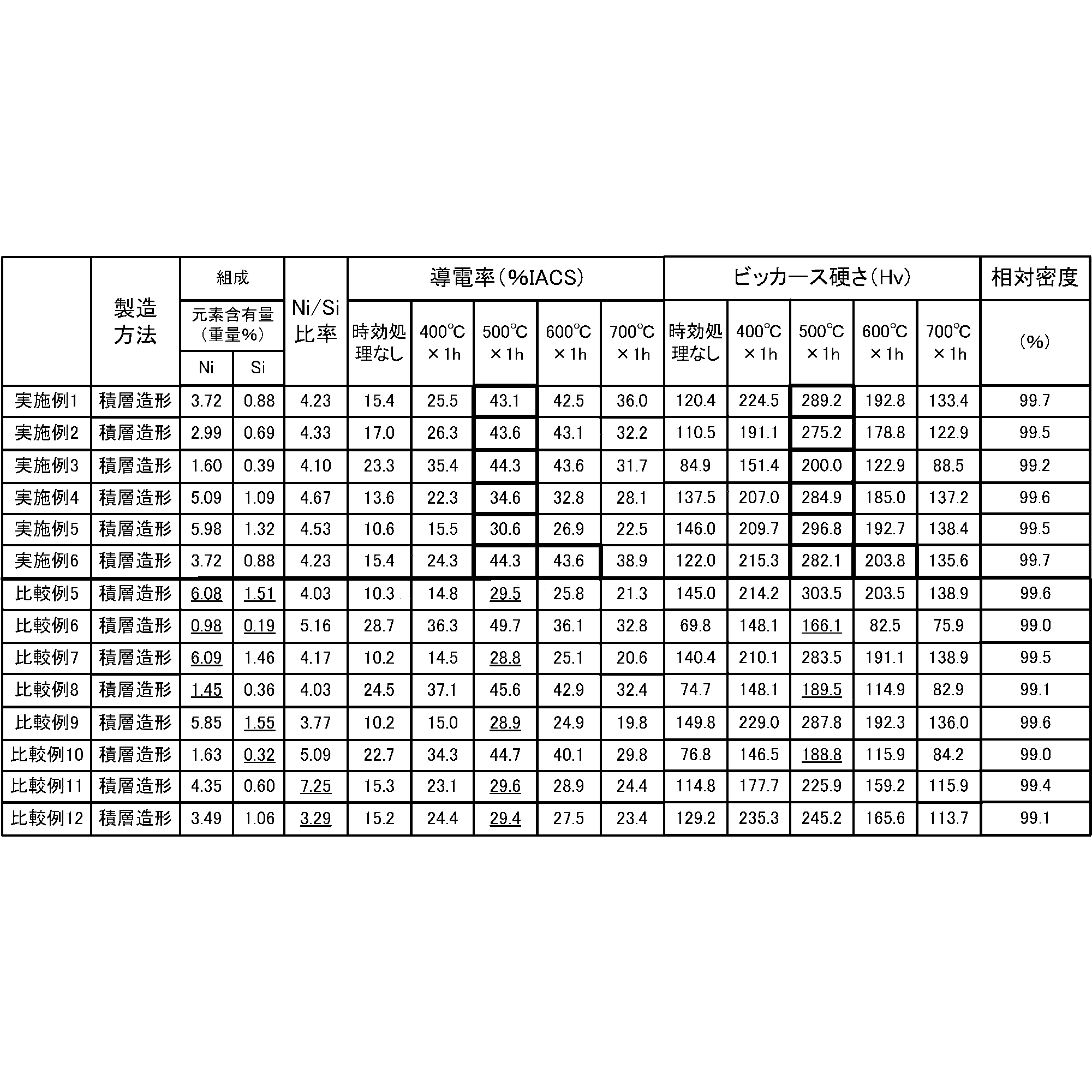
実施例1~6は、積層造形用銅合金粉末の、ニッケルおよびシリコンの含有量および比率、および、特性が条件範囲内であるため、所定の時効処理によって十分な導電率(30%IACS以上)と強度(ビッカース硬さ:200Hv以上)とを兼ね備えた銅合金積層造形体を造形できた。
In Examples 1 to 6, the content and ratio of nickel and silicon, and the properties of the copper alloy powder for additive manufacturing are within the required range, so that sufficient electrical conductivity (30% IACS or more) is achieved by the prescribed aging treatment. It was possible to fabricate a copper alloy laminate-molded body having both high strength and strength (Vickers hardness: 200 Hv or more).
一方、比較例5ではニッケルおよびシリコンの含有量が過剰で条件範囲外であるため、高いビッカース硬さを示すものの、導電率は低い値となった。比較例6ではニッケルおよびシリコンの含有量が過少で条件範囲外であるため、導電率は高いもののビッカース硬さが低い値となった。比較例7ではニッケルの含有量が過剰であり、比較例9ではシリコンの含有量が過剰であるため、高いビッカース硬さを示すものの、導電率は低い値となった。比較例8ではニッケルの含有量が過少であり、比較例10ではシリコンの含有量が過少であるため、導電率は高いもののビッカース硬さが低い値となった。
On the other hand, in Comparative Example 5, the contents of nickel and silicon were excessive and outside the condition range, so although it exhibited high Vickers hardness, the conductivity was a low value. In Comparative Example 6, the contents of nickel and silicon were too low and were out of the range of conditions, so although the conductivity was high, the Vickers hardness was low. Comparative Example 7 had an excessive nickel content, and Comparative Example 9 had an excessive silicon content, so although it exhibited high Vickers hardness, its conductivity was low. In Comparative Example 8, the nickel content was too low, and in Comparative Example 10, the silicon content was too low, so although the conductivity was high, the Vickers hardness was low.
ニッケルの含有量(重量%)をシリコンの含有量(重量%)で除した値(比率)に関しては、比較例11では7.2を上回っているため、比較例12では3.3を下回っているため、高いビッカース硬さを示すものの、導電率は低い値となった。
Regarding the value (ratio) obtained by dividing the nickel content (wt%) by the silicon content (wt%), it exceeds 7.2 in Comparative Example 11, and is less than 3.3 in Comparative Example 12. Therefore, although it exhibited high Vickers hardness, its conductivity was low.
図1は、実施例1~6および比較例5~12において、時効処理500℃の導電率(%IACS)をX軸にとり、ビッカース硬さ(Hv)をY軸にとって、特性をプロットした図である。
Figure 1 is a diagram plotting the characteristics of Examples 1 to 6 and Comparative Examples 5 to 12, with the electrical conductivity (%IACS) at 500°C aging treatment taken on the X axis and the Vickers hardness (Hv) taken on the Y axis. be.
実施例1~6の銅合金積層造形体の導電率およびビッカース硬さが条件範囲を満たす一方と、比較例5~12の銅合金積層造形体の導電率およびビッカース硬さが条件範囲を満たさないことが明らかである。
While the electrical conductivity and Vickers hardness of the copper alloy laminate-molded bodies of Examples 1 to 6 satisfy the condition range, the electrical conductivity and Vickers hardness of the copper alloy laminate-molded bodies of Comparative Examples 5 to 12 do not satisfy the condition range. That is clear.
また、図2は、実施例1~6において、時効処理の温度を400℃から700℃に変化させた場合の、導電率(%IACS)またはビッカース硬さ(Hv)の特性をプロットした図である。
Furthermore, Figure 2 is a diagram plotting the characteristics of electrical conductivity (%IACS) or Vickers hardness (Hv) when the aging treatment temperature was changed from 400°C to 700°C in Examples 1 to 6. be.
実施例1~6における時効処理の温度範囲が、450℃以上550℃以下が望ましく、導電率を高くしたい場合は550℃が好ましく、ビッカース硬さを高くしたい場合は500℃が好ましいことが分かる。
It can be seen that the temperature range of the aging treatment in Examples 1 to 6 is preferably 450 ° C. or higher and 550 ° C. or lower, preferably 550 ° C. if you want to increase the conductivity, and 500 ° C. if you want to increase the Vickers hardness.
<ニッケルおよびシリコンと、他金属元素とを含有する積層造形用銅合金粉末の実施例>
ニッケルとシリコンとの含有量および含有比率と、他の金属元素の含有量とを変化させて積層造形用銅合金粉末を製造し、次に積層造形用銅合金粉末を用いて積層造形された銅合金積層造形体を製造し、それらの特性を測定した。 <Example of copper alloy powder for additive manufacturing containing nickel, silicon, and other metal elements>
Copper alloy powder for additive manufacturing is manufactured by changing the content and content ratio of nickel and silicon and the content of other metal elements, and then copper is produced by additive manufacturing using the copper alloy powder for additive manufacturing. Alloy additively manufactured bodies were manufactured and their properties were measured.
(積層造形用銅合金粉末の製造と特性測定)
ガスアトマイズ法により、表3に示したニッケルおよびシリコンと、他の金属元素とを含有する銅合金の積層造形用銅合金粉末を製造した。そして、得られた積層造形用銅合金粉末を、レーザ方式粉末床溶融法向けとして粒径10μm以上45μm以下に、電子ビーム方式粉末床溶融法向けとして粒径45μm以上105μm以下となるように分級した。 (Production and property measurement of copper alloy powder for additive manufacturing)
A copper alloy powder for additive manufacturing of a copper alloy containing nickel and silicon and other metal elements shown in Table 3 was produced by a gas atomization method. The obtained copper alloy powder for additive manufacturing was classified into a particle size of 10 μm or more and 45 μm or less for laser powder bed melting, and a particle size of 45 μm or more and 105 μm or less for electron beam powder bed melting. .
ICP発光分光分析法により、得られた積層造形用銅合金粉末における成分元素の含有量を測定した。また、JIS Z 2504に準じて、得られた積層造形用銅合金粉末の見掛密度(AD)(g/cm3)を測定した。また、JIS Z 2502に準じて、得られた積層造形用銅合金粉末の流動度(FR)(sec/50g)を測定した。また、レーザ回折法により50%粒径(D50)(μm)を測定した(マイクロトラックMT3300:マイクロトラックベル株式会社製)。
The content of component elements in the obtained copper alloy powder for additive manufacturing was measured by ICP emission spectroscopy. Further, the apparent density (AD) (g/cm 3 ) of the obtained copper alloy powder for additive manufacturing was measured according to JIS Z 2504. Further, the flow rate (FR) (sec/50 g) of the obtained copper alloy powder for additive manufacturing was measured according to JIS Z 2502. Further, the 50% particle size (D50) (μm) was measured by laser diffraction method (Microtrac MT3300: manufactured by Microtrac Bell Co., Ltd.).
パウダーレオメータFT4(フリーマンテクノロジー社製)を用いてせん断試験を実施し、得られた積層造形用銅合金粉末の付着力(kPa)を測定した。得られた積層造形用銅合金粉末のスキージング性は、3D積層造形機(粉末焼結積層造形/レーザ方式もしくは電子ビーム方式)の造形ステージにて実際に、造形試験に供する粉末を敷き詰めて粉末層を形成することで評価した。実施例10~19の積層造形用銅合金粉末についての各特性の測定結果を表3に示した。
A shear test was conducted using a powder rheometer FT4 (manufactured by Freeman Technology), and the adhesion force (kPa) of the obtained copper alloy powder for additive manufacturing was measured. The squeezing property of the obtained copper alloy powder for additive manufacturing was measured by actually spreading the powder to be used for the modeling test on the modeling stage of a 3D additive manufacturing machine (powder sintering additive manufacturing/laser method or electron beam method). Evaluation was made by forming a layer. Table 3 shows the measurement results of each characteristic of the copper alloy powders for additive manufacturing of Examples 10 to 19.

(積層造形用銅合金粉末を用いた銅合金積層造形体の製造)
実施例10~13および15~19の積層造形用銅合金粉末を用いて、波長1064nmのYbファイバレーザ搭載の3D粉末積層造形機(SLM Solutions GmbH、SLM280HL)にて試験に供する積層造形体を製造した。積層造形は、積層厚25μm以上50μm以下、レーザ出力300W以上700W以下、走査速度900mm/sec以上1500mm/sec以下、エネルギー密度150J/mm3以上450J/mm3以下の条件で行った。 (Manufacture of copper alloy additive manufacturing object using copper alloy powder for additive manufacturing)
Using the copper alloy powders for additive manufacturing of Examples 10 to 13 and 15 to 19, a laminate manufactured body for testing was produced using a 3D powder additive manufacturing machine (SLM Solutions GmbH, SLM280HL) equipped with a Yb fiber laser with a wavelength of 1064 nm. did. The additive manufacturing was performed under the following conditions: a layer thickness of 25 μm or more and 50 μm or less, a laser output of 300 W or more and 700 W or less, a scanning speed of 900 mm/sec or more and 1500 mm/sec or less, and an energy density of 150 J/mm 3 or more and 450 J/mm 3 or less.
実施例14における積層造形用銅合金粉末を用いて、電子ビーム搭載の3D粉末積層造形機(ArcamAB、EBM A2X)にて試験に供する積層造形体を製造した。積層造形は、積層厚が50μm以上100μm以下、電子ビーム電圧が60kV、予備加熱温度が300℃以上700℃以下の条件で行った。積層造形においては、3D粉末積層造形機を用いてφ14mm、高さ10mmである円柱状の積層造形体を製造した。
Using the copper alloy powder for additive manufacturing in Example 14, a laminate model to be tested was manufactured using a 3D powder additive manufacturing machine (ArcamAB, EBM A2X) equipped with an electron beam. The additive manufacturing was performed under the conditions that the layer thickness was 50 μm or more and 100 μm or less, the electron beam voltage was 60 kV, and the preheating temperature was 300° C. or more and 700° C. or less. In the additive manufacturing, a cylindrical additive-molded body having a diameter of 14 mm and a height of 10 mm was manufactured using a 3D powder additive manufacturing machine.
(銅合金積層造形体の特性測定)
実施例10~19の銅合金積層造形用粉末を用いて製造した積層造形体の相対密度(%)を、置換媒体としてヘリウムガスを使用したアルキメデス法により測定した(AccuPyc1330:株式会社島津製作所製)。測定結果は表4に示した。 (Measurement of characteristics of copper alloy laminate manufactured object)
The relative density (%) of the additively manufactured objects produced using the copper alloy additively manufactured powders of Examples 10 to 19 was measured by the Archimedes method using helium gas as a replacement medium (AccuPyc1330: manufactured by Shimadzu Corporation). . The measurement results are shown in Table 4.
3D粉末積層造形機にて製造した実施例10~19の銅合金積層造形体について、導電率(%IACS)を渦流式導電率計で測定した(高性能渦流式導電率計 シグマチェック:日本マテック株式会社製)。また、銅合金積層造形体のビッカース硬さ(Hv)を、微小硬さ試験機で測定した(微小硬さ試験機HMV-G21-DT:株式会社島津製作所製)。
The electrical conductivity (%IACS) of the copper alloy additive bodies of Examples 10 to 19 manufactured using a 3D powder additive manufacturing machine was measured using an eddy current conductivity meter (high performance eddy current conductivity meter Sigma Check: Nippon Matec) Co., Ltd.). In addition, the Vickers hardness (Hv) of the copper alloy laminate-molded body was measured using a microhardness tester (microhardness tester HMV-G21-DT: manufactured by Shimadzu Corporation).
作製した銅合金積層造形体に、不活性雰囲気中で、400℃、500℃、600℃および700℃に温度を設定して1時間の時効処理を施した。時効処理を施した銅合金積層造形体の導電率を、渦流式導電率計で測定した。また、ビッカース硬さを微小硬さ試験機で測定した。3D粉末積層造形機にて製造した実施例10~19の積層造形体について、各種特性の評価結果を表4に示した。表4中、太枠で囲った特性の値は、銅合金積層造形体としての条件範囲を満たす値を示す。
The prepared copper alloy laminate was subjected to aging treatment for 1 hour at temperatures set at 400°C, 500°C, 600°C, and 700°C in an inert atmosphere. The conductivity of the aged copper alloy laminate was measured using an eddy current conductivity meter. In addition, Vickers hardness was measured using a microhardness tester. Table 4 shows the evaluation results of various properties of the additively molded bodies of Examples 10 to 19 manufactured using the 3D powder additive manufacturing machine. In Table 4, the values of the properties surrounded by thick frames indicate values that satisfy the condition range as a copper alloy layered product.

実施例10~19は、積層造形用銅合金粉末の、ニッケルおよびシリコンの含有量および比率、および、特性が条件範囲内であるため、所定の時効処理によって十分な導電率(30%IACS以上)と強度(ビッカース硬さ:200Hv以上)とを兼ね備えた銅合金積層造形体を造形できた。
In Examples 10 to 19, the content and ratio of nickel and silicon, and the properties of the copper alloy powder for additive manufacturing are within the required range, so that sufficient electrical conductivity (30% IACS or more) is achieved by the prescribed aging treatment. It was possible to fabricate a copper alloy laminate-molded body having both high strength and strength (Vickers hardness: 200 Hv or more).
図3は、実施例10~19において、時効処理500℃の導電率(%IACS)をX軸にとり、ビッカース硬さ(Hv)をY軸にとって、特性をプロットした図である。
FIG. 3 is a graph plotting the characteristics of Examples 10 to 19, with the electrical conductivity (%IACS) at 500°C aging treatment taken on the X axis and the Vickers hardness (Hv) taken on the Y axis.
実施例10~19の銅合金積層造形体の導電率およびビッカース硬さが条件範囲を満たす一方、比較例5~12の銅合金積層造形体の導電率およびビッカース硬さが条件範囲を満たさないことが明らかである。
While the electrical conductivity and Vickers hardness of the copper alloy laminate-molded bodies of Examples 10 to 19 satisfy the condition range, the electrical conductivity and Vickers hardness of the copper alloy laminate-molded bodies of Comparative Examples 5 to 12 do not satisfy the condition range. is clear.
また、ニッケル、シリコンおよび鉄を含有する銅合金積層造形体である実施例10および11は、同等のニッケルおよびシリコンを含有し、かつ鉄を含有しない銅合金積層造形体である実施例1と比較して、導電率の低下を抑えつつ、時効処理温度によらずビッカース硬さが大きく向上している。
In addition, Examples 10 and 11, which are copper alloy layered products containing nickel, silicon, and iron, are compared with Example 1, which is a copper alloy layered product that contains equivalent nickel and silicon, but does not contain iron. As a result, the Vickers hardness is greatly improved regardless of the aging temperature while suppressing the decrease in electrical conductivity.
ニッケル、シリコンおよび銀を含有する銅合金積層造形体である実施例15は、同等のニッケルおよびシリコンを含有し、かつ銀を含有しない銅合金積層造形体である実施例1と比較して、ビッカース硬さはほぼ同等ながら、導電率が向上している。また、実施例16では導電率は同等の値を維持しつつ、ビッカース硬さが向上している。
Example 15, which is a copper alloy laminate-molded body containing nickel, silicon, and silver, has a higher Vickers laminate than Example 1, which is a copper alloy laminate-molded body that contains equivalent nickel and silicon but does not contain silver. Although the hardness is almost the same, the conductivity is improved. Furthermore, in Example 16, the Vickers hardness was improved while maintaining the same electrical conductivity.
ニッケル、シリコンおよびマグネシウムを含有する銅合金積層造形体である実施例17は、同等のニッケルおよびシリコンを含有し、かつマグネシウムを含有しない銅合金積層造形体である実施例2と比較して、導電率の低下を抑えつつ、ビッカース硬さが向上している。
Example 17, which is a copper alloy laminate-molded body containing nickel, silicon, and magnesium, has higher conductivity than Example 2, which is a copper alloy laminate-molded body that contains equivalent nickel and silicon but does not contain magnesium. Vickers hardness has been improved while suppressing the decrease in hardness.
ニッケル、シリコン、マグネシウムおよびマンガンを含有する銅合金積層造形体である実施例18は、同等のニッケルおよびシリコンを含有し、かつマグネシウムとマンガンをいずれも含有しない銅合金積層造形体である実施例1と比較して、500℃時効処理におけるビッカース硬さが大きく向上している。
Example 18, which is a copper alloy layered product containing nickel, silicon, magnesium, and manganese, is Example 1, which is a copper alloy layered product containing equivalent nickel and silicon, and containing neither magnesium nor manganese. The Vickers hardness after aging treatment at 500°C is significantly improved compared to the above.
ニッケル、シリコン、錫および亜鉛を含有する銅合金積層造形体である実施例19は、同等のニッケルおよびシリコンを含有し、かつ錫と亜鉛をいずれも含有しない銅合金積層造形体である実施例3と比較して、ビッカース硬さが熱処理条件によらず向上している。
Example 19, which is a copper alloy layered product containing nickel, silicon, tin, and zinc, is Example 3, which is a copper alloy layered product containing equivalent nickel and silicon, and containing neither tin nor zinc. The Vickers hardness is improved regardless of the heat treatment conditions.
また、図4は、実施例10~19において、時効処理の温度を400℃から700℃に変化させた場合の、導電率(%IACS)またはビッカース硬さ(Hv)の特性をプロットした図である。
Furthermore, FIG. 4 is a diagram plotting the characteristics of electrical conductivity (%IACS) or Vickers hardness (Hv) when the aging treatment temperature was changed from 400°C to 700°C in Examples 10 to 19. be.
実施例10~19における時効処理の温度範囲が、450℃以上550℃以下が望ましく、導電率を高くしたい場合は550℃が好ましく、ビッカース硬さを高くしたい場合は500℃が好ましいことが分かる。
It can be seen that the temperature range of the aging treatment in Examples 10 to 19 is preferably 450 ° C. or higher and 550 ° C. or lower, preferably 550 ° C. if you want to increase the electrical conductivity, and 500 ° C. if you want to increase the Vickers hardness.
<アーク溶解または圧延加工による、ニッケルおよびシリコンを含有する銅合金造形体の比較例>
(アーク溶製材)
鋳造したコルソン合金インゴットに塑性加工および溶体化処理を施す従来の製造方法を用いて作製した銅合金(コルソン合金)の特性と、実施例1~6および10~19の銅合金積層造形体の特性を比較するため、以下の方法を用いて従来法で作製されたコルソン合金の特性評価を行った。鋳造材製造方法の代わりとして、公知の溶製材製造方法であるアーク溶解法を用いた。 <Comparative example of copper alloy shaped bodies containing nickel and silicon produced by arc melting or rolling processing>
(arc melting lumber)
Characteristics of a copper alloy (Corson alloy) produced using a conventional manufacturing method in which a cast Corson alloy ingot is subjected to plastic working and solution treatment, and characteristics of copper alloy laminate manufactured bodies of Examples 1 to 6 and 10 to 19 In order to compare the characteristics of Corson alloys produced by conventional methods, we performed the following methods. As an alternative to the method for producing cast materials, an arc melting method, which is a known method for producing molten materials, was used.
実施例1~5、10~13および15~19と同様の積層造形用銅合金粉末を使用してアーク溶解を行い、アーク溶製材を作製した。アーク溶製材は以下に示した通りに作製した。まず、実施例1~5、10~13および15~19の積層造形用銅合金粉末をプレス成形して、圧粉体を作製した。作製した圧粉体を、日新技研株式会社製の真空アーク溶解炉を用いてアルゴン雰囲気中でアーク溶解し、アーク溶製材を作製した。このアーク溶製材を比較例21~34とした。なお、実施例6は実施例1と同一組成であり、実施例14は実施例10と同一組成であるため、実施例6、14と同様の積層造形用銅合金粉末を使用したアーク溶製材は作製しなかった。
Arc melting was performed using the same copper alloy powder for additive manufacturing as in Examples 1 to 5, 10 to 13, and 15 to 19 to produce arc melted materials. The arc melted lumber was produced as shown below. First, the copper alloy powders for additive manufacturing of Examples 1 to 5, 10 to 13, and 15 to 19 were press-molded to produce green compacts. The produced compact was arc melted in an argon atmosphere using a vacuum arc melting furnace manufactured by Nissin Giken Co., Ltd. to produce an arc melted material. These arc-melted materials were designated as Comparative Examples 21 to 34. In addition, since Example 6 has the same composition as Example 1, and Example 14 has the same composition as Example 10, the arc-melted material using the same copper alloy powder for additive manufacturing as Examples 6 and 14 is Not created.
アーク溶解にて作製した比較例21~34のアーク溶製材について、導電率(%IACS)を渦流式導電率計で測定した(高性能渦流式導電率計 シグマチェック:日本マテック株式会社製)。また、ビッカース硬さ(Hv)を、微小硬さ試験機で測定した(微小硬さ試験機HMV-G21-DT:株式会社島津製作所製)。
The electrical conductivity (%IACS) of the arc melted materials of Comparative Examples 21 to 34 produced by arc melting was measured using an eddy current conductivity meter (high performance eddy current conductivity meter Sigma Check: manufactured by Nippon Matek Co., Ltd.). In addition, Vickers hardness (Hv) was measured using a microhardness tester (microhardness tester HMV-G21-DT: manufactured by Shimadzu Corporation).
また、作製したアーク溶製材に、不活性雰囲気中で、400および500、600、700℃に温度を設定して1時間の時効処理を施した。時効処理を施したアーク溶製材の導電率を、渦流式導電率計で測定した。また、ビッカース硬さを微小硬さ試験機で測定した。
In addition, the produced arc melted materials were subjected to aging treatment for 1 hour at temperatures set at 400, 500, 600, and 700°C in an inert atmosphere. The electrical conductivity of the aged arc melted lumber was measured using an eddy current conductivity meter. In addition, Vickers hardness was measured using a microhardness tester.
比較例21~34のアーク溶製材について、各種特性の評価結果を表5に示した。表5中、アンダーラインを付した特性の値は、500℃の時効処理においても銅合金造形体としての条件範囲を満たさない値を示す。
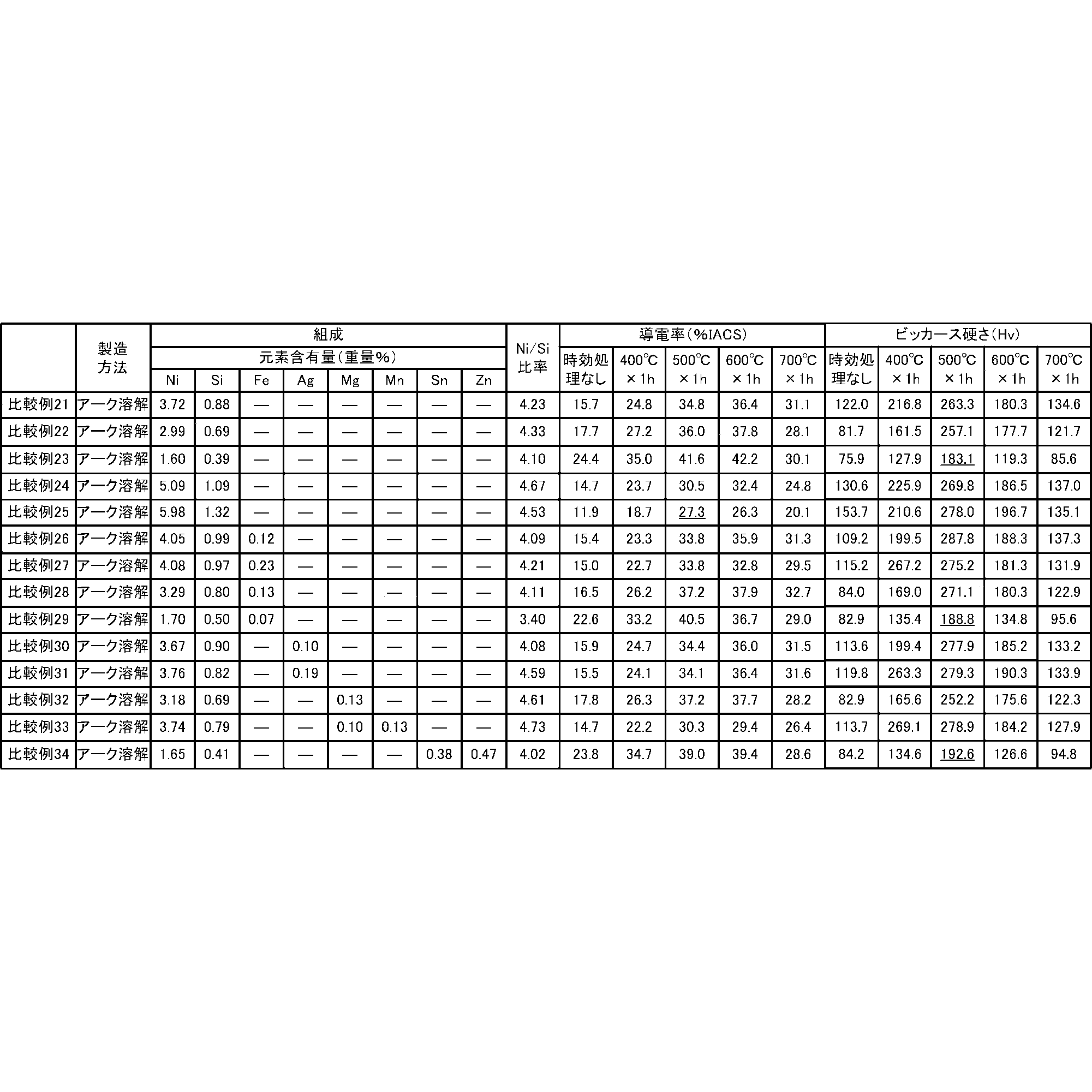
Table 5 shows the evaluation results of various properties of the arc-melted materials of Comparative Examples 21 to 34. In Table 5, the underlined property values indicate values that do not satisfy the condition range for a copper alloy shaped body even after aging treatment at 500°C.
(圧延加工したアーク溶製材)
次に、得られた比較例21~34のアーク溶製材を、圧延装置を用いて加工率50%で圧延し、塑性加工を行った。その圧延体に、不活性雰囲気中で950℃に温度を設定して1時間の溶体化処理を施した。この圧延加工を加えたアーク溶製材を比較例41~54とした。 (Rolled arc melted lumber)
Next, the obtained arc-melted materials of Comparative Examples 21 to 34 were rolled at a processing rate of 50% using a rolling machine to perform plastic working. The rolled body was subjected to solution treatment for 1 hour at a temperature of 950° C. in an inert atmosphere. The arc-melted materials subjected to this rolling process were designated as Comparative Examples 41 to 54.
比較例21~34のアーク溶製材に圧延加工を加えたアーク溶製材の比較例41~54について、導電率(%IACS)を渦流式導電率計で測定した(高性能渦流式導電率計 シグマチェック:日本マテック株式会社製)。また、ビッカース硬さ(Hv)を、微小硬さ試験機で測定した(微小硬さ試験機HMV-G21-DT:株式会社島津製作所製)。
The electrical conductivity (%IACS) of Comparative Examples 41 to 54, which were obtained by rolling the arc-molten materials of Comparative Examples 21 to 34, was measured using an eddy current conductivity meter (high-performance eddy current conductivity meter Sigma). Check: Manufactured by Nippon Matek Co., Ltd.). In addition, Vickers hardness (Hv) was measured using a microhardness tester (microhardness tester HMV-G21-DT: manufactured by Shimadzu Corporation).
圧延加工を加えたアーク溶製材に、不活性雰囲気中で、400および500、600、700℃に温度を設定して1時間の時効処理を施した。時効処理を施した圧延加工を加えたアーク溶製材の導電率を、渦流式導電率計で測定した。また、ビッカース硬さを微小硬さ試験機で測定した。
The rolled arc-melted material was aged in an inert atmosphere at temperatures of 400, 500, 600, and 700°C for 1 hour. The electrical conductivity of the arc melted sawn material that had been subjected to aging treatment and rolling processing was measured using an eddy current conductivity meter. In addition, Vickers hardness was measured using a microhardness tester.
比較例41~54の圧延加工を加えたアーク溶製材について、各種特性の評価結果を表6に示した。表6中、アンダーラインを付した特性の値は、500℃の時効処理においても銅合金造形体としての条件範囲を満たさない値を示す。

Table 6 shows the evaluation results of various properties of the arc-melted materials subjected to rolling processing in Comparative Examples 41 to 54. In Table 6, the underlined property values indicate values that do not satisfy the condition range for a copper alloy shaped body even after aging treatment at 500°C.
図5は、時効処理500℃における、実施例1~6および10~19の銅合金積層造形体の特性と、比較例21~34のアーク溶製材と、比較例41~54の圧延加工を加えたアーク溶製材との特性を、導電率(%IACS)をX軸にとり、ビッカース硬さ(Hv)をY軸にとってプロットした図である。
Figure 5 shows the characteristics of the copper alloy laminate manufactured bodies of Examples 1 to 6 and 10 to 19 after aging treatment at 500°C, the arc melted materials of Comparative Examples 21 to 34, and the rolling processing of Comparative Examples 41 to 54. It is a diagram plotting the characteristics of arc-molten material with electrical conductivity (%IACS) on the X-axis and Vickers hardness (Hv) on the Y-axis.
比較例21~34のアーク溶製材は、溶体化処理後に強加工を施して歪みを加えていないので、熱処理を施しても実施例1~6および10~19の特性よりも劣っている。従来の製造方法を模して作製した圧延加工を加えた比較例41~54のアーク溶製材の特性と比較して、実施例1~6および10~19の銅合金積層造形体は遜色ない特性を実現できている。
The arc-melted materials of Comparative Examples 21 to 34 were not strained by strong working after solution treatment, so even after heat treatment, the properties were inferior to those of Examples 1 to 6 and 10 to 19. Compared to the characteristics of the arc-molten materials of Comparative Examples 41 to 54, which were produced by imitating conventional manufacturing methods and added rolling processing, the copper alloy laminate products of Examples 1 to 6 and 10 to 19 had comparable characteristics. has been achieved.
以上のことから、実施例1~6および10~19によれば、溶体化処理および塑性加工プロセスを要することなく、高導電率(熱伝導率)および優れた機械的強度を両立した、積層造形用銅合金粉末、および銅合金積層造形体を提供可能であることが確認された。
From the above, according to Examples 1 to 6 and 10 to 19, additive manufacturing that achieves both high electrical conductivity (thermal conductivity) and excellent mechanical strength without requiring solution treatment and plastic working processes. It was confirmed that it is possible to provide a copper alloy powder for use in copper alloys and a copper alloy laminate-molded body.
Claims (13)
- 積層造形法により積層造形体を造形するために用いられる積層造形用銅合金粉末であって、
ニッケルおよびシリコンを含有し、残部が銅および不可避的不純物からなり、
前記ニッケルの含有量(重量%)を前記シリコンの含有量(重量%)で除した値が3.3以上7.2以下である積層造形用銅合金粉末。 A copper alloy powder for additive manufacturing used for forming a additively manufactured object by an additive manufacturing method,
Contains nickel and silicon, with the remainder consisting of copper and unavoidable impurities,
A copper alloy powder for additive manufacturing in which the value obtained by dividing the nickel content (wt%) by the silicon content (wt%) is 3.3 or more and 7.2 or less. - 前記ニッケルを1.5重量%以上6.0重量%以下含有する請求項1に記載の積層造形用銅合金粉末。 The copper alloy powder for additive manufacturing according to claim 1, containing the nickel in an amount of 1.5% by weight or more and 6.0% by weight or less.
- 前記シリコンを0.35重量%以上1.5重量%以下含有する請求項2に記載の積層造形用銅合金粉末。 The copper alloy powder for additive manufacturing according to claim 2, containing the silicon at 0.35% by weight or more and 1.5% by weight or less.
- 50%粒径が3μm以上200μm以下である請求項1から3のいずれか1項に記載の積層造形用銅合金粉末。 The copper alloy powder for additive manufacturing according to any one of claims 1 to 3, having a 50% particle size of 3 μm or more and 200 μm or less.
- JIS Z 2504(ISO 3923-1)の測定法で測定したときの粉末の見掛密度が3.5g/cm3以上である請求項1から3のいずれか1項に記載の積層造形用銅合金粉末。 The copper alloy for additive manufacturing according to any one of claims 1 to 3, wherein the powder has an apparent density of 3.5 g/cm 3 or more when measured by the measuring method of JIS Z 2504 (ISO 3923-1). powder.
- せん断試験によって得られた破壊包絡線から求めた銅合金粉末の付着力が、0.600kPa以下である請求項1から3のいずれか1項に記載の積層造形用銅合金粉末。 The copper alloy powder for additive manufacturing according to any one of claims 1 to 3, wherein the adhesion force of the copper alloy powder determined from the fracture envelope obtained by a shear test is 0.600 kPa or less.
- さらに、鉄、銀、マグネシウム、マンガン、錫および亜鉛から選択される1種または2種以上を合計で1.0重量%(ただし、鉄、銀、マグネシウム、マンガン、錫、および亜鉛が0重量%である場合を除く)まで含有する請求項1から3のいずれか1項に記載の積層造形用銅合金粉末。 Furthermore, a total of 1.0% by weight of one or more selected from iron, silver, magnesium, manganese, tin, and zinc (with the exception of 0% by weight of iron, silver, magnesium, manganese, tin, and zinc). The copper alloy powder for additive manufacturing according to any one of claims 1 to 3, further comprising a copper alloy powder for additive manufacturing according to any one of claims 1 to 3.
- 請求項1に記載の積層造形用銅合金粉末を用いて、積層造形装置により積層造形された銅合金積層造形体であって、
ニッケルの含有量(重量%)をシリコンの含有量(重量%)で除した値が3.3以上7.2以下である銅合金積層造形体。 A copper alloy additively manufactured body produced by additively manufacturing with an additively manufacturing apparatus using the copper alloy powder for additively manufactured according to claim 1,
A copper alloy laminate-produced article in which the value obtained by dividing the nickel content (wt%) by the silicon content (wt%) is 3.3 or more and 7.2 or less. - 請求項3に記載の積層造形用銅合金粉末を用いて、積層造形装置により積層造形された銅合金積層造形体であって、
ニッケルの含有量(重量%)をシリコンの含有量(重量%)で除した値が3.3以上7.2以下であり、
前記ニッケルを1.5重量%以上6.0重量%以下、および、前記シリコンを0.35重量%以上1.5重量%以下含有し、残部が銅および不可避的不純物からなる銅合金積層造形体。 A copper alloy laminate-manufactured body manufactured by a laminate-manufacturing apparatus using the copper alloy powder for laminate-manufacturing according to claim 3,
The value obtained by dividing the nickel content (wt%) by the silicon content (wt%) is 3.3 or more and 7.2 or less,
A copper alloy laminate-produced article containing 1.5% by weight or more and 6.0% by weight or less of the nickel and 0.35% by weight or more and 1.5% by weight or less of the silicon, with the balance being copper and inevitable impurities. . - 請求項8または9に記載の銅合金積層造形体であって、
30%IACS以上の導電率、および、200Hv以上のビッカース硬さを有する銅合金積層造形体。 The copper alloy laminate-molded article according to claim 8 or 9,
A copper alloy laminate-molded body having an electrical conductivity of 30% IACS or more and a Vickers hardness of 200 Hv or more. - 請求項7に記載の積層造形用銅合金粉末を用いて、積層造形装置により積層造形された銅合金積層造形体であって、
ニッケルの含有量(重量%)をシリコンの含有量(重量%)で除した値が3.3以上7.2以下であり、
前記ニッケルを1.5重量%以上6.0重量%以下、前記シリコンを0.35重量%以上1.5重量%以下、および、鉄、銀、マグネシウム、マンガン、錫、および亜鉛から選択される1種または2種以上を合計で1.0重量%(ただし、鉄、銀、マグネシウム、マンガン、錫、および亜鉛が0重量%である場合を除く)まで含有し、残部が銅および不可避的不純物からなる銅合金積層造形体。 A copper alloy laminate-manufactured body manufactured by a laminate-manufacturing apparatus using the copper alloy powder for laminate-manufacturing according to claim 7,
The value obtained by dividing the nickel content (wt%) by the silicon content (wt%) is 3.3 or more and 7.2 or less,
The nickel is selected from 1.5% by weight or more and 6.0% by weight or less, the silicon is selected from 0.35% by weight or more and 1.5% by weight or less, and iron, silver, magnesium, manganese, tin, and zinc. Contains one or more types up to a total of 1.0% by weight (excluding cases where iron, silver, magnesium, manganese, tin, and zinc are 0% by weight), with the remainder being copper and unavoidable impurities. A copper alloy additively manufactured body consisting of. - 請求項11に記載の銅合金積層造形体であって、
30%IACS以上の導電率、および、200Hv以上のビッカース硬さを有する銅合金積層造形体。 The copper alloy laminate-molded article according to claim 11,
A copper alloy laminate-molded body having an electrical conductivity of 30% IACS or more and a Vickers hardness of 200 Hv or more. - 請求項1から3のいずれか1項に記載の積層造形用銅合金粉末を用いて、積層造形装置により銅合金積層造形体を積層造形する積層造形工程と、
前記銅合金積層造形体を、450℃以上550℃以下で保持する時効処理工程と、
を含む銅合金積層造形体の製造方法。 A layered manufacturing step of layer-manufacturing a copper alloy layered object using a layered manufacturing device using the copper alloy powder for layered manufacturing according to any one of claims 1 to 3;
an aging treatment step of holding the copper alloy layered product at a temperature of 450° C. or higher and 550° C. or lower;
A method for manufacturing a copper alloy layered product including:
Priority Applications (1)
| Application Number | Priority Date | Filing Date | Title |
|---|---|---|---|
| PCT/JP2022/025245 WO2023248453A1 (en) | 2022-06-24 | 2022-06-24 | Copper alloy powder for additive manufacturing, additively manufactured copper alloy article, and method for manufacturing copper alloy additively-manufactured article |
Applications Claiming Priority (1)
| Application Number | Priority Date | Filing Date | Title |
|---|---|---|---|
| PCT/JP2022/025245 WO2023248453A1 (en) | 2022-06-24 | 2022-06-24 | Copper alloy powder for additive manufacturing, additively manufactured copper alloy article, and method for manufacturing copper alloy additively-manufactured article |
Publications (1)
| Publication Number | Publication Date |
|---|---|
| WO2023248453A1 true WO2023248453A1 (en) | 2023-12-28 |
Family
ID=89379328
Family Applications (1)
| Application Number | Title | Priority Date | Filing Date |
|---|---|---|---|
| PCT/JP2022/025245 WO2023248453A1 (en) | 2022-06-24 | 2022-06-24 | Copper alloy powder for additive manufacturing, additively manufactured copper alloy article, and method for manufacturing copper alloy additively-manufactured article |
Country Status (1)
| Country | Link |
|---|---|
| WO (1) | WO2023248453A1 (en) |
Citations (6)
| Publication number | Priority date | Publication date | Assignee | Title |
|---|---|---|---|---|
| JPH0931571A (en) * | 1995-07-17 | 1997-02-04 | Hitachi Powdered Metals Co Ltd | Wear resistant copper base sintered alloy |
| JP2005256147A (en) * | 2004-03-15 | 2005-09-22 | Toyota Motor Corp | Overlaying abrasion-resistant copper-based alloy |
| JP2011157630A (en) * | 2002-07-05 | 2011-08-18 | Olin Corp | Copper alloy containing cobalt, nickel, and silicon |
| WO2018062527A1 (en) * | 2016-09-29 | 2018-04-05 | Jx金属株式会社 | Surface treatment metal powder for laser sintering |
| JP2018123405A (en) * | 2017-02-03 | 2018-08-09 | 日産自動車株式会社 | Method for manufacturing laminate member |
| US20180311736A1 (en) * | 2017-04-28 | 2018-11-01 | Te Connectivity Corporation | System and Method for Forming Nano-Particles in Additively-Manufactured Metal Alloys |
-
2022
- 2022-06-24 WO PCT/JP2022/025245 patent/WO2023248453A1/en unknown
Patent Citations (6)
| Publication number | Priority date | Publication date | Assignee | Title |
|---|---|---|---|---|
| JPH0931571A (en) * | 1995-07-17 | 1997-02-04 | Hitachi Powdered Metals Co Ltd | Wear resistant copper base sintered alloy |
| JP2011157630A (en) * | 2002-07-05 | 2011-08-18 | Olin Corp | Copper alloy containing cobalt, nickel, and silicon |
| JP2005256147A (en) * | 2004-03-15 | 2005-09-22 | Toyota Motor Corp | Overlaying abrasion-resistant copper-based alloy |
| WO2018062527A1 (en) * | 2016-09-29 | 2018-04-05 | Jx金属株式会社 | Surface treatment metal powder for laser sintering |
| JP2018123405A (en) * | 2017-02-03 | 2018-08-09 | 日産自動車株式会社 | Method for manufacturing laminate member |
| US20180311736A1 (en) * | 2017-04-28 | 2018-11-01 | Te Connectivity Corporation | System and Method for Forming Nano-Particles in Additively-Manufactured Metal Alloys |
Similar Documents
| Publication | Publication Date | Title |
|---|---|---|
| JP7314184B2 (en) | Method for manufacturing parts made of aluminum alloy | |
| EP3616810A1 (en) | High-strength aluminum alloy laminated molding and production method therefor | |
| WO2019239655A1 (en) | Copper alloy powder, layered/molded product, method for producing layered/molded product, and metal parts | |
| CN110872658B (en) | High-performance copper alloy and powder preparation method thereof | |
| JP2016053198A (en) | Metal molded product and metal powder for metal molded product | |
| JP2017155291A (en) | Manufacturing method of high strength aluminum alloy laminate molded body | |
| JPH02503331A (en) | Magnesium alloy with high mechanical resistance and manufacturing method by rapid solidification of the alloy | |
| CN113348262A (en) | Method for manufacturing aluminum alloy parts | |
| JP2005314806A (en) | Powder of nano crystalline copper metal and nano crystalline copper alloy having high hardness and high electric conductivity, bulk material of nano crystalline copper or copper alloy having high hardness, high strength, high electric conductivity and high toughness, and production method thereof | |
| CN112805107B (en) | Method for manufacturing aluminum alloy parts | |
| EP3804879A1 (en) | Cu-based alloy powder | |
| CN111014703B (en) | Preparation method of nickel-based alloy powder for laser cladding | |
| EP4083244A1 (en) | Heat-resistant powdered aluminium material | |
| CN113423524B (en) | Method for manufacturing aluminum alloy parts | |
| WO2015146604A1 (en) | SPUTTERING TARGET COMPRISING Ni-P ALLOY OR Ni-Pt-P ALLOY AND PRODUCTION METHOD THEREFOR | |
| WO2023248453A1 (en) | Copper alloy powder for additive manufacturing, additively manufactured copper alloy article, and method for manufacturing copper alloy additively-manufactured article | |
| EP3760342A1 (en) | Copper alloy powder having excellent laser absorptivity | |
| JP7394241B2 (en) | Copper alloy powder for additive manufacturing and its evaluation method, method for producing a copper alloy additive manufacturing object, and copper alloy additive manufacturing object | |
| WO2023181329A1 (en) | Copper alloy powder for additive layer manufacturing, production method and evaluation method therefor, method for producing additive layer-manufactured copper alloy article, and additive layer-manufactured copper alloy article | |
| JP6583019B2 (en) | Cu-Ga alloy sputtering target and method for producing Cu-Ga alloy sputtering target | |
| JP7422095B2 (en) | sputtering target material | |
| KR20230009373A (en) | Method for manufacturing aluminum alloy parts | |
| JP2022122462A (en) | Carbon-fixed carbon steel powder | |
| JP2005082855A (en) | Al ALLOY MATERIAL | |
| US20240123502A1 (en) | Titanium alloy powder for selective laser melting 3d printing, selective laser melted titanium alloy and preparation thereof |
Legal Events
| Date | Code | Title | Description |
|---|---|---|---|
| 121 | Ep: the epo has been informed by wipo that ep was designated in this application |
Ref document number: 22948014 Country of ref document: EP Kind code of ref document: A1 |