WO2023243538A1 - Light source unit and video display device - Google Patents
Light source unit and video display device Download PDFInfo
- Publication number
- WO2023243538A1 WO2023243538A1 PCT/JP2023/021396 JP2023021396W WO2023243538A1 WO 2023243538 A1 WO2023243538 A1 WO 2023243538A1 JP 2023021396 W JP2023021396 W JP 2023021396W WO 2023243538 A1 WO2023243538 A1 WO 2023243538A1
- Authority
- WO
- WIPO (PCT)
- Prior art keywords
- display device
- light
- image
- source unit
- light source
- Prior art date
Links
- 230000003287 optical effect Effects 0.000 claims abstract description 138
- 238000009826 distribution Methods 0.000 claims abstract description 44
- 230000015572 biosynthetic process Effects 0.000 claims abstract description 9
- 238000003384 imaging method Methods 0.000 claims description 72
- 238000006243 chemical reaction Methods 0.000 claims description 28
- 238000005452 bending Methods 0.000 claims description 13
- 238000010586 diagram Methods 0.000 description 42
- 230000000694 effects Effects 0.000 description 24
- 238000000149 argon plasma sintering Methods 0.000 description 16
- 239000004065 semiconductor Substances 0.000 description 14
- 239000010410 layer Substances 0.000 description 13
- 230000004048 modification Effects 0.000 description 11
- 238000012986 modification Methods 0.000 description 11
- 239000000463 material Substances 0.000 description 10
- 239000011347 resin Substances 0.000 description 7
- 229920005989 resin Polymers 0.000 description 7
- 239000010408 film Substances 0.000 description 6
- 230000007423 decrease Effects 0.000 description 5
- 239000011159 matrix material Substances 0.000 description 5
- 239000011241 protective layer Substances 0.000 description 5
- 239000000758 substrate Substances 0.000 description 5
- 230000009471 action Effects 0.000 description 4
- 230000005684 electric field Effects 0.000 description 4
- 239000011521 glass Substances 0.000 description 4
- 210000003128 head Anatomy 0.000 description 4
- OAICVXFJPJFONN-UHFFFAOYSA-N Phosphorus Chemical compound [P] OAICVXFJPJFONN-UHFFFAOYSA-N 0.000 description 3
- 229910052751 metal Inorganic materials 0.000 description 3
- 239000002184 metal Substances 0.000 description 3
- 239000007769 metal material Substances 0.000 description 3
- 230000008859 change Effects 0.000 description 2
- 238000013461 design Methods 0.000 description 2
- 238000000034 method Methods 0.000 description 2
- 239000002245 particle Substances 0.000 description 2
- 230000010287 polarization Effects 0.000 description 2
- 239000002096 quantum dot Substances 0.000 description 2
- 239000010409 thin film Substances 0.000 description 2
- 229910002601 GaN Inorganic materials 0.000 description 1
- JMASRVWKEDWRBT-UHFFFAOYSA-N Gallium nitride Chemical compound [Ga]#N JMASRVWKEDWRBT-UHFFFAOYSA-N 0.000 description 1
- 239000004642 Polyimide Substances 0.000 description 1
- XUIMIQQOPSSXEZ-UHFFFAOYSA-N Silicon Chemical compound [Si] XUIMIQQOPSSXEZ-UHFFFAOYSA-N 0.000 description 1
- NINIDFKCEFEMDL-UHFFFAOYSA-N Sulfur Chemical compound [S] NINIDFKCEFEMDL-UHFFFAOYSA-N 0.000 description 1
- GWEVSGVZZGPLCZ-UHFFFAOYSA-N Titan oxide Chemical compound O=[Ti]=O GWEVSGVZZGPLCZ-UHFFFAOYSA-N 0.000 description 1
- 238000007792 addition Methods 0.000 description 1
- 238000013459 approach Methods 0.000 description 1
- 239000002131 composite material Substances 0.000 description 1
- 150000001875 compounds Chemical class 0.000 description 1
- 230000008878 coupling Effects 0.000 description 1
- 238000010168 coupling process Methods 0.000 description 1
- 238000005859 coupling reaction Methods 0.000 description 1
- 238000012217 deletion Methods 0.000 description 1
- 230000037430 deletion Effects 0.000 description 1
- 230000002542 deteriorative effect Effects 0.000 description 1
- 239000003989 dielectric material Substances 0.000 description 1
- 238000009792 diffusion process Methods 0.000 description 1
- 210000000887 face Anatomy 0.000 description 1
- 230000004313 glare Effects 0.000 description 1
- 239000011810 insulating material Substances 0.000 description 1
- 239000004973 liquid crystal related substance Substances 0.000 description 1
- 238000004519 manufacturing process Methods 0.000 description 1
- 230000007246 mechanism Effects 0.000 description 1
- 239000002114 nanocomposite Substances 0.000 description 1
- 239000002105 nanoparticle Substances 0.000 description 1
- 239000002070 nanowire Substances 0.000 description 1
- 229910052698 phosphorus Inorganic materials 0.000 description 1
- 239000011574 phosphorus Substances 0.000 description 1
- 239000004417 polycarbonate Substances 0.000 description 1
- 229920000515 polycarbonate Polymers 0.000 description 1
- 229920001721 polyimide Polymers 0.000 description 1
- 229920000642 polymer Polymers 0.000 description 1
- 239000002861 polymer material Substances 0.000 description 1
- 238000007788 roughening Methods 0.000 description 1
- 238000000926 separation method Methods 0.000 description 1
- 238000004904 shortening Methods 0.000 description 1
- 229910052710 silicon Inorganic materials 0.000 description 1
- 239000010703 silicon Substances 0.000 description 1
- 229910052717 sulfur Inorganic materials 0.000 description 1
- 239000011593 sulfur Substances 0.000 description 1
- OGIDPMRJRNCKJF-UHFFFAOYSA-N titanium oxide Inorganic materials [Ti]=O OGIDPMRJRNCKJF-UHFFFAOYSA-N 0.000 description 1
- 239000012780 transparent material Substances 0.000 description 1
Images


Classifications
-
- B—PERFORMING OPERATIONS; TRANSPORTING
- B60—VEHICLES IN GENERAL
- B60K—ARRANGEMENT OR MOUNTING OF PROPULSION UNITS OR OF TRANSMISSIONS IN VEHICLES; ARRANGEMENT OR MOUNTING OF PLURAL DIVERSE PRIME-MOVERS IN VEHICLES; AUXILIARY DRIVES FOR VEHICLES; INSTRUMENTATION OR DASHBOARDS FOR VEHICLES; ARRANGEMENTS IN CONNECTION WITH COOLING, AIR INTAKE, GAS EXHAUST OR FUEL SUPPLY OF PROPULSION UNITS IN VEHICLES
- B60K35/00—Arrangement of adaptations of instruments
-
- G—PHYSICS
- G02—OPTICS
- G02B—OPTICAL ELEMENTS, SYSTEMS OR APPARATUS
- G02B27/00—Optical systems or apparatus not provided for by any of the groups G02B1/00 - G02B26/00, G02B30/00
- G02B27/01—Head-up displays
-
- G—PHYSICS
- G02—OPTICS
- G02B—OPTICAL ELEMENTS, SYSTEMS OR APPARATUS
- G02B5/00—Optical elements other than lenses
- G02B5/04—Prisms
Definitions
- Embodiments relate to a light source unit and an image display device.
- Patent Document 1 discloses that light emitted from a display device capable of displaying an image is sequentially reflected by a plurality of mirrors, and the light reflected by the last mirror is further directed toward the user by a reflective member such as a windshield.
- a technique is disclosed in which a virtual image is reflected and allows a user to view a virtual image corresponding to an image displayed by a display device. There is a demand for miniaturization of such devices.
- the embodiments of the present invention have been made in view of the above-mentioned problems, and an object thereof is to provide a light source unit and an image display device that can be downsized.
- a light source unit includes a display device capable of displaying an image, a first prism sheet into which light emitted from the display device enters, and an imaging optical system.
- the imaging optical system includes an input element into which the light emitted from the first prism sheet enters, and an output element into which the light that has passed through the input element enters, and the light emitted from the output element forms the image.
- a first image is formed according to the image.
- the imaging optical system has substantially telecentricity on the first image side.
- the light emitted from the display device has a substantially Lambertian light distribution.
- An image display device includes the light source unit and a reflection unit that is spaced apart from the light source unit and reflects light emitted from the imaging optical system.
- the first image is formed between the light source unit and the reflection unit.
- FIG. 1 is an end view showing a video display device according to a first embodiment.
- FIG. 2 is a plan view showing the display device of the light source unit according to the first embodiment.
- FIG. 3A is a perspective view showing the first prism sheet of the light source unit according to the first embodiment.
- FIG. 3B is an end view showing the first prism sheet of the light source unit according to the first embodiment.
- FIG. 3C is an end view showing the first prism sheet of the light source unit according to the first embodiment.
- FIG. 4 is an end view showing the display device of the video display device according to the first embodiment.
- FIG. 5A is an optical diagram showing the action of the second prism in the first embodiment.
- FIG. 5B is a diagram showing pixels of a display device.
- FIG. 5C is a diagram showing pixels magnified by the first prism.
- FIG. 5D is a diagram showing pixels further enlarged by the second prism.
- FIG. 6 is a schematic diagram showing the scenery seen from a viewer in the driver's seat in the first embodiment.
- FIG. 7A is a schematic diagram showing the principle of the light source unit according to the first embodiment.
- FIG. 7B is a schematic diagram showing the principle of a light source unit according to a reference example.
- FIG. 8A is a graph showing a light distribution pattern of light emitted from one light emitting area in Examples 1, 11 and Reference Example.
- FIG. 8B is a graph showing the uniformity of brightness of the second image in Examples 1 to 12 and the reference example.
- FIG. 9 is a plan view showing a display device in the second embodiment.
- FIG. 9 is a plan view showing a display device in the second embodiment.
- FIG. 10A is a plan view showing a prism sheet in the second embodiment.
- FIG. 10B is an end view taken along the line XB-XB shown in FIG. 10A.
- FIG. 11 is a plan view showing a display device and a prism sheet in the second embodiment.
- FIG. 12A is a diagram showing a state in which some pixels are lit in a display device.
- FIG. 12B is a diagram showing pixels enlarged by the first prism.
- FIG. 13A is an end view showing the display device and the first prism sheet of the second embodiment.
- FIG. 13B is an optical diagram showing the first prism of this embodiment.
- FIG. 13C is an equation showing the relationship among distance, prism angle, refractive index, and pixel shift amount.
- FIG. 13C is an equation showing the relationship among distance, prism angle, refractive index, and pixel shift amount.
- FIG. 13D is a graph showing the relationship between the distance required to obtain a desired pixel shift amount and the prism angle, with the horizontal axis representing the pixel shift amount and the vertical axis representing the prism angle.
- FIG. 14A is a diagram showing the distribution of light transmitted through the first prism sheet, and shows a case where the ratio of prism pitch to distance is 1.5%.
- FIG. 14B is a diagram showing the distribution of light transmitted through the first prism sheet, and shows a case where the ratio of prism pitch to distance is 5.0%.
- FIG. 15 is a plan view showing the first prism sheet of the third embodiment.
- FIG. 16A is a diagram showing one pixel in the third embodiment.
- FIG. 16B is a diagram showing pixels enlarged by the first prism.
- FIG. 16C is a diagram showing pixels further enlarged by the second prism.
- FIG. 17A is a diagram showing an image displayed by a display device in the third embodiment.
- FIG. 17B is a diagram showing an image enlarged by the first prism.
- FIG. 17C is a diagram showing an image further enlarged by the second prism.
- FIG. 18A is a side view showing a display device, a first prism sheet, and a second prism sheet of a light source unit according to the fourth embodiment.
- FIG. 18B is a plan view showing the first prism sheet of the fourth embodiment.
- FIG. 18C is a plan view showing the second prism sheet of the fourth embodiment.
- FIG. 18A is a side view showing a display device, a first prism sheet, and a second prism sheet of a light source unit according to the fourth embodiment.
- FIG. 18B is a plan view showing the first prism sheet of the fourth embodiment.
- FIG. 18C is a plan view showing the second prism
- FIG. 19 is a side view showing a display device, a first prism sheet, a second prism sheet, and a third prism sheet of a light source unit according to the fifth embodiment.
- FIG. 20A is a plan view showing the first prism sheet of the fifth embodiment.
- FIG. 20B is a plan view showing the second prism sheet of the fifth embodiment.
- FIG. 20C is a plan view showing the third prism sheet of the fifth embodiment.
- FIG. 21A is a schematic diagram showing the operation of the fifth embodiment.
- FIG. 21B is a schematic diagram showing the operation of the fifth embodiment.
- FIG. 21C is a schematic diagram showing the operation of the fifth embodiment.
- FIG. 21D is a schematic diagram showing the operation of the fifth embodiment.
- FIG. 22 is a perspective view showing the first prism sheet of the sixth embodiment.
- FIG. 23 is an end view showing a video display device according to the seventh embodiment.
- FIG. 24 is a schematic diagram showing the scenery seen from the viewer in the driver's seat in the seventh embodiment.
- FIG. 25 is an end view showing a video display device according to the eighth embodiment.
- FIG. 26 is an enlarged cross-sectional view of a part of the display device and reflective polarizing element shown in FIG. 25.
- FIG. 27 is a side view showing a light source unit according to the ninth embodiment.
- FIG. 28 is a side view showing a light source unit according to a modification of the ninth embodiment.
- FIG. 1 is an end view showing a video display device according to this embodiment.
- FIG. 2 is a plan view showing the display device of the light source unit according to this embodiment.
- FIG. 3A is a perspective view showing the first prism sheet of the light source unit according to this embodiment.
- 3B and 3C are end views showing the first prism sheet of the light source unit according to this embodiment.
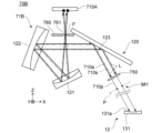
- the video display device 10 includes a light source unit 11 and a reflection unit 12.
- the light source unit 11 includes a display device 110, an imaging optical system 120, and a first prism sheet 130.
- the display device 110 has a plurality of pixels and can display images. Light emitted from the display device 110 enters the first prism sheet 130 .
- the imaging optical system 120 receives the light emitted from the first prism sheet 130 and forms a first image IM1 corresponding to the image displayed by the display device 110.
- the first image IM1 is a real image and an intermediate image.
- the reflection unit 12 is spaced apart from the light source unit 11 and reflects the light emitted from the imaging optical system 120.
- the video display device 10 is mounted on, for example, a car 1000 and constitutes a HUD (Head Up Display).
- the automobile 1000 includes a vehicle 13 and a video display device 10 fixed to the vehicle 13.
- the viewer 14 is a passenger of the automobile 1000, for example, a driver.
- the display device 110 of the light source unit 11 displays an image that is desired to be viewed by the viewer 14 using the HUD.
- the first prism sheet 130 refracts the light emitted from each pixel of the display device 110 and expands the area where the light emitted from each pixel reaches. This mechanism will be described later.
- the imaging optical system 120 outputs the light emitted from the first prism sheet 130 to the reflection unit 12, and forms a first image IM1 between the light source unit 11 and the reflection unit 12.
- the reflection unit 12 reflects the light emitted from the light source unit 11 toward the front windshield 13a of the vehicle 13.
- the front windshield 13a includes, for example, glass.
- the front windshield 13a reflects the light arriving from the reflection unit 12 on its inner surface and makes it enter the eyebox 14a of the viewer 14. Thereby, the viewer 14 can visually recognize the second image IM2 corresponding to the image displayed by the display device 110 on the other side of the front windshield 13a.
- the second image IM2 is a virtual image larger than the first image IM1.
- the "eye box" refers to the area in front of the viewer's eyes where a virtual image can be viewed.
- the longitudinal direction of the vehicle 13 is referred to as the "X direction”
- the left-right direction of the vehicle 13 is referred to as the "Y direction”
- the vertical direction of the vehicle 13 is referred to as the "Z direction.”
- the XY plane is a horizontal plane of the vehicle 13.
- the direction of the arrow forward
- the opposite direction backward
- the direction of the arrow (to the left) is referred to as the "+Y direction”, and the opposite direction (to the right) is also referred to as the "-Y direction”.
- the direction of the arrow (upward) is referred to as the "+Z direction”
- the opposite direction (downward) is also referred to as the "-Z direction”.
- the position where the first image IM1 is formed is indicated by a circular mark. Similar to the first image IM1, the position where the second image IM2 is formed is also indicated by a circular mark.
- the positions from which the principal ray L that reaches each mark of the first image IM1 is emitted are indicated by square marks. In this way, in order to make the explanation easier to understand, the emission position of each principal ray L on the display device 110 is set to a different mark from the imaging position of the first image IM1 and the imaging position of the second image IM2. As shown in , the image displayed on the display device 110, the first image IM1, and the second image IM2 have a generally similar relationship.
- unit areas 110u are arranged in a matrix along the third direction and the fourth direction, and every other unit area 110u is arranged in the third direction and the fourth direction.
- a pixel 110p is arranged at 110u.
- one pixel 110p is arranged for every four unit areas 110u arranged in 2 rows and 2 columns.
- the plurality of pixels 110p are arranged in a staggered manner along the third direction and the fourth direction.
- the fourth direction intersects, for example, is orthogonal to the third direction.
- the third direction is the horizontal direction of the image
- the fourth direction is the vertical direction of the image.
- the third direction is the X direction
- the fourth direction is the Y direction.
- the light emitted from the display device 110 has a substantially Lambertian light distribution. The specific configuration of the display device 110 and the Lambertian light distribution will be described in detail later.
- the first prism sheet 130 has a first surface 130a onto which light emitted from the display device 110 enters, and a second surface 130b opposite to the first surface 130a.
- the second surface 130b emits light toward the imaging optical system 120.
- a striped first prism 130p1 extending in the fourth direction (Y direction) is formed on the first surface 130a of the first prism sheet 130, and a striped first prism 130p1 extending in the third direction (X direction) is formed on the second surface 130b.
- An extending stripe-shaped second prism 130p2 is formed.
- the first prism sheet 130 When viewed from the ⁇ Z direction, the first prism sheet 130 is the same as or larger than the display device 110 and covers the display device 110. Furthermore, the arrangement period of the first prisms 130p1 in the X direction is shorter than the arrangement period of the unit area 110u of the display device 110 in the X direction. Similarly, the arrangement period of the second prisms 130p2 in the Y direction is shorter than the arrangement period of the unit regions 110u in the Y direction. Thereby, the light emitted from each pixel 110p of the display device 110 always enters one or more first prisms 130p1 and one or more second prisms 130p2.
- FIG. 4 is an end view showing the display device of the video display device according to this embodiment.
- the display device 110 of the light source unit 11 is an LED display.
- a plurality of LED elements 112 are arranged in a staggered manner.
- One or more LED elements 112 are arranged in each pixel 110p of the display device 110.
- each LED element 112 is mounted face down on the substrate 111.
- each LED element may be mounted face-up on the board.
- Each LED element 112 has a semiconductor stack 112a, an anode electrode 112b, and a cathode electrode 112c.
- the substrate 111 is made of an insulating material such as resin or glass.
- a silicon semiconductor chip for driving each LED element 112 can also be used for the substrate 111.
- the semiconductor stack 112a includes a p-type semiconductor layer 112p1, an active layer 112p2 placed on the p-type semiconductor layer 112p1, and an n-type semiconductor layer 112p3 placed on the active layer 112p2.
- a gallium nitride-based compound semiconductor represented by In X Al Y Ga 1-XY N (0 ⁇ X, 0 ⁇ Y, X+Y ⁇ 1) is used for the semiconductor stack 112a.
- the light emitted by the LED element 112 is visible light in this embodiment.
- the anode electrode 112b is electrically connected to the p-type semiconductor layer 112p1. Further, the anode electrode 112b is electrically connected to the wiring 118b.
- the cathode electrode 112c is electrically connected to the n-type semiconductor layer 112p3. Further, the cathode electrode 112c is electrically connected to another wiring 118a.
- a metal material can be used for each electrode 112b, 112c.
- a plurality of recesses 112t are provided on the light exit surface 112s of each LED element 112.
- the term "light exit surface of the LED element” refers to the surface of the LED element from which the light incident on the imaging optical system 120 mainly exits.
- the surface of the n-type semiconductor layer 112p3 located on the opposite side of the surface facing the active layer 112p2 corresponds to the light exit surface 112s.
- optical axis C the optical axis of light emitted from each pixel 110p will be simply referred to as "optical axis C.”
- the optical axis C is parallel to the XY plane on which the plurality of pixels 110p are arranged, and the light from one pixel 110p is irradiated on the first plane P1 located on the light emission side of the display device 110.
- the brightness is at the point a1 in the range where the light from this pixel 110p is irradiated on the second plane P2 which is parallel to the XY plane and is separated from the first plane P1.
- This is a straight line connecting the maximum point a2.
- the center point of those points may be set as the point where the brightness is maximum. Note that from a productivity standpoint, it is desirable that the optical axis C be parallel to the Z axis.
- the light emitted from each LED element 112 is transmitted as indicated by the broken line in FIG. As shown, it has a substantially Lambertian light distribution.
- the light emitted from each pixel has a substantially Lambertian light distribution
- the luminous intensity in the direction of the angle ⁇ with respect to the optical axis C of each pixel is on the optical axis C, where n is a value larger than 0. This means that the light distribution pattern can be approximated by cos n ⁇ times the luminous intensity of .
- n is preferably 11 or less, and even more preferably 1.
- the light distribution pattern of the light emitted from this pixel 110p in each plane is approximately Lambertian light distribution, and The numerical values of n are also approximately equal.
- the imaging optical system 120 of the light source unit 11 is an optical system that includes all optical elements necessary to form the first image IM1 at a predetermined position.
- the light emitted from the output element 123 forms a first image IM1. Note that the light that has passed through the input element 121 may enter the output element 123, and the intermediate element 122 may not be provided.
- the imaging optical system 120 has approximately telecentricity on the first image IM1 side.
- the different positions are, for example, different pixels 110p of the display device 110.
- the plurality of principal rays L are substantially parallel means that they are substantially parallel within a practical range that allows for errors due to manufacturing precision, assembly precision, etc. of the components of the light source unit 11.
- the angle between the principal rays L is 10 degrees or less.
- the imaging optical system 120 When the imaging optical system 120 has substantially telecentricity on the first image IM1 side, the plurality of principal rays L intersect with each other before entering the input element 121.
- the point where the plurality of principal rays L intersect with each other will be referred to as a "focal point F.” Therefore, whether or not the imaging optical system 120 has substantially telecentricity on the first image IM1 side can be confirmed by the following method using, for example, the retrograde property of light.
- a light source capable of emitting parallel light such as a laser light source, is placed near the position where the first image IM1 is formed.
- the output element 123 of the imaging optical system 120 is irradiated with light emitted from this light source.
- the imaging optical system 120 has approximately telecentricity on the first image IM1 side. It can be determined that there is.
- the imaging optical system 120 Since the imaging optical system 120 has substantially telecentricity on the first image IM1 side, the imaging optical system 120 includes light that passes through the focal point F and its vicinity, out of the light emitted from each pixel of the display device 110. is mainly incident. Each optical element constituting the imaging optical system 120 will be described below.
- the input element 121 is located on the ⁇ Z side of the display device 110 and is arranged to face the display device 110.
- the input element 121 is a mirror having a concave mirror surface 121a.
- the input element 121 reflects the light emitted from the display device 110.
- the intermediate element 122 is located on the -X side of the display device 110 and the input element 121, and is arranged to face the input element 121.
- the intermediate element 122 is a mirror having a concave mirror surface 122a. Intermediate element 122 further reflects the light reflected by input element 121.
- the input element 121 and the intermediate element 122 constitute a bending portion 120a that bends the plurality of principal rays L so that the plurality of principal rays L emitted from different positions of the display device 110 are substantially parallel to each other.
- the mirror surfaces 121a and 122a are biconic surfaces in this embodiment. However, the mirror surface may be a part of a spherical surface or may be a free-form surface.
- the output element 123 is located on the +X side of the display device 110 and the input element 121, and is arranged to face the intermediate element 122.
- the output element 123 is a mirror having a flat mirror surface 123a.
- the output element 123 reflects the light that has passed through the input element 121 and the intermediate element 122 toward the formation position of the first image IM1. Specifically, a plurality of principal rays L that are substantially parallel due to the bending portion 120a are incident on the output element 123.
- the mirror surface 123a is inclined with respect to the XY plane, which is the horizontal plane of the vehicle 13, so that the more it goes in the -Z direction, the more it goes in the +X direction.
- the output element 123 reflects the light reflected by the intermediate element 122 in a direction inclined with respect to the Z direction such that the more it goes in the -Z direction, the more it goes in the +X direction.
- the output element 123 directs the plurality of principal rays L so that the plurality of principal rays L, which have become substantially parallel due to the bending portion 120a, head toward the formation position P of the first image IM1.
- a direction changing unit 120b for changing the direction is configured.
- the optical path between the input element 121 and the intermediate element 122 extends in a direction intersecting the XY plane. Further, the optical path between the intermediate element 122 and the output element 123 extends in a direction along the XY plane. Since a part of the optical path within the imaging optical system 120 extends in a direction intersecting the XY plane, the light source unit 11 can be downsized to some extent in the direction along the XY plane. Furthermore, since the other part of the optical path within the imaging optical system 120 extends in the direction along the XY plane, the light source unit 11 can be downsized to some extent in the Z direction.
- the optical path between the display device 110 and the input element 121 intersects with the optical path between the intermediate element 122 and the output element 123. In this way, by making the optical paths intersect with each other within the light source unit 11, the light source unit 11 can be made smaller.
- optical path within the light source unit is not limited to the above.
- all optical paths within the imaging optical system may extend in a direction along the XY plane, or may extend in a direction intersecting the XY plane. Further, the optical paths within the light source unit do not need to intersect with each other.
- the input element 121, the intermediate element 122, and the output element 123 each include a main body member made of glass or a resin material, and a metal film or dielectric material provided on the surface of the main body member and forming mirror surfaces 121a, 122a, and 123a. It may also be configured with a reflective film such as a multilayer film. Further, the input element 121, the intermediate element 122, and the output element 123 may each be entirely made of a metal material.
- the light source unit 11 is provided on the ceiling portion 13b of the vehicle 13.
- the light source unit 11 is arranged, for example, inside a wall 13s1 exposed inside the vehicle at the ceiling portion 13b.
- the wall 13s1 is provided with a through hole 13h1 through which light emitted from the output element 123 of the light source unit 11 can pass.
- the light emitted from the output element 123 passes through the through hole 13h1 and is irradiated into the space between the viewer 14 and the front windshield 13a.
- the light source unit may be attached to the ceiling surface.
- the through hole 13h1 may be provided with a transparent or translucent cover having a small haze value.
- the haze value is preferably 50% or less, and even more preferably 20% or less.
- the configuration and position of the coupling optical system are not limited to the above as long as it has substantially telecentricity on the first image side.
- the number of optical elements constituting the direction changing section may be two or more.
- the reflection unit 12 includes a mirror 131 having a concave mirror surface 131a.
- Mirror 131 is arranged to face front windshield 13a.
- the mirror 131 reflects the light emitted from the output element 123 and irradiates it onto the front windshield 13a.
- the mirror 131 may include a main body member made of glass, a resin material, or the like, and a reflective film such as a metal film or a dielectric multilayer film provided on the surface of the main body member and forming the mirror surface 131a. Further, the mirror 131 may be entirely made of a metal material.
- mirror surface 131a is a biconic surface. However, the mirror surface may be a part of a spherical surface or may be a free-form surface.
- the light irradiated onto the front windshield 13a is reflected on the inner surface of the front windshield 13a and enters the eye box 14a of the viewer 14. Thereby, the viewer 14 visually recognizes the second image IM2 corresponding to the image displayed on the display device 110 on the other side of the front windshield 13a.
- the reflection unit 12 is provided on the dashboard portion 13c of the vehicle 13.
- the reflection unit 12 is arranged, for example, inside a wall 13s2 of the dashboard portion 13c of the vehicle 13 that is exposed inside the vehicle.
- the wall 13s2 is provided with a through hole 13h2 through which light emitted from the output element 123 of the light source unit 11 can pass.
- the light emitted from the output element 123 passes through the through hole 13h1 to form a first image IM1, and then passes through the through hole 13h2 and is irradiated onto the reflection unit 12.
- the reflection unit may be attached to the upper surface of the dashboard part.
- the reflection unit may be placed on the ceiling and the light source unit may be placed on the dashboard.
- the path of light from the inner surface of the front windshield 13a toward the eyebox 14a is generally horizontal, completely horizontal, or slightly inclined so that the eyebox 14a side is higher. That is, this path is approximately parallel to the XY plane.
- the light source unit 11 is placed above (+Z direction) and the reflection unit 12 is placed below (-Z direction) with respect to the XY plane including the path of this light. That is, the light source unit 11 and the reflection unit 12 are separated from each other with the XY plane interposed therebetween.
- the configuration and position of the reflection unit are not limited to the above.
- the number of optical elements such as mirrors constituting the reflection unit may be two or more.
- the reflection unit 12 needs to be arranged so that, for example, sunlight irradiated from outside the vehicle through the front windshield 13a is not reflected toward the eye box 14a.
- FIG. 5A is an optical diagram showing the action of the second prism 130p2 in this embodiment.
- FIG. 5B is a diagram showing the pixel 110p of the display device 110.
- FIG. 5C is a diagram showing pixels enlarged by the first prism 130p1.
- FIG. 5D is a diagram showing pixels further enlarged by the second prism 130p2.
- FIG. 6 is a schematic diagram showing the scenery seen from the viewer in the driver's seat in this embodiment.
- the light emitted from the pixel 110p of the display device 110 is separated in the Y direction by the second prism 130p2 of the first prism sheet 130, and the area where the light reaches expands in the Y direction.
- the light emitted from the pixel 110p is separated in the X direction by the first prism 130p1, and the area where the light reaches expands in the X direction. Therefore, when the light emitted from the pixel 110p passes through the first prism sheet 130, the area where the light reaches expands in the X direction and the Y direction.
- FIG. 5B shows two pixels 110p of the display device 110.
- the pixels 110p are spaced apart from each other.
- the first prism 130p1 of the first prism sheet 130 it is separated in the X direction as shown in FIG. 5C.
- each pixel 110p appears to be separated into two pixels 110p along the X direction.
- pixel separation refers to the fact that light emitted from one pixel is separated by a prism and the pixel appears to be separated when viewed from the viewer 14 side.
- each pixel 110p shown in FIG. 5C appears to be separated into two pixels 110p along the Y direction. Therefore, the light emitted from the pixel 110p is spread in the X direction and the Y direction by the action of the first prism 130p1 and the second prism 130p2, and the area of the region where the light reaches is, for example, four times the area of the pixel 110p.
- the light beam L is emitted from the first prism sheet 130.
- the imaging optical system 120 of the light source unit 11 forms a first image IM1, which is a real image, at position P.
- the light forming the first image IM1 is reflected by the reflection unit 12 and the front windshield 13a, and enters the eyebox 14a of the viewer 14.
- the viewer 14 visually recognizes the second image IM2, which is a virtual image, on the other side of the front windshield 13a.
- the second image IM2 is shown as a character string "information", but the second image IM2 is not limited to a character string, and may be a figure or the like.
- pixels 110p are arranged in every other unit region 110u in the X direction and the Y direction.
- the image enlargement ratio that is, the ratio of the size of the second image IM2 to the size of the image displayed by the display device 110 can be reduced, and the imaging optical system 120 can be made smaller.
- the display device 110 becomes larger, the imaging optical system 120 becomes smaller, so that the light source unit 11 as a whole can be made smaller. Therefore, the video display device 10 can also be downsized.
- the distance between the pixels 110p of the display device 110 becomes less visible in the second image IM2.
- the quality of the second image IM2 can be made equal to that when the pixels 110p are not separated from each other.
- the light emitted from the pixels can be expanded using a diffusion sheet or the like, but by using a prism sheet as in this embodiment, the emitted light can be expanded while suppressing a decrease in brightness. be able to.
- the pixels 110p are arranged in every other unit area 110u in the X direction and the Y direction, and the first prism sheet 130 extends the area where the light emitted from the pixel 110p reaches in the X direction.
- the present invention is not limited to this.
- pixels 110p are arranged in every other unit region 110u only in the X direction, pixels 110p are arranged in all unit regions 110u arranged continuously in the Y direction, and the first prism sheet 130 may be provided with only the first prism 130p1 and may not be provided with the second prism 130p2.
- pixels 110p are arranged in every other unit region 110u only in the Y direction, pixels 110p are arranged in all continuously arranged unit regions 110u in the X direction, and the first prism Only the second prism 130p2 may be provided on the sheet 130, and the first prism 130p1 may not be provided.
- one pixel 110p is arranged in every second or more unit area 110u in the X direction and the Y direction, and the first prism sheet 130 increases the area where the light emitted from the pixel 110p reaches three times in the X direction and the Y direction. It may be more than that.
- first prism 130p1 and the second prism 130p2 are provided on one first prism sheet 130
- the present invention is not limited to this, and the first prism 130p1 and the second prism 130p2 may be provided separately on two prism sheets.
- FIG. 7A is a schematic diagram showing the principle of the light source unit according to this embodiment.
- FIG. 7B is a schematic diagram showing the principle of a light source unit according to a reference example.
- FIG. 7A the light distribution pattern of light emitted from two pixels 110p of the plurality of pixels 110p of the display device 110 in this embodiment is shown by broken lines.
- FIG. 7B the light distribution pattern of light emitted from two pixels 2110p of the plurality of pixels 2110p of the display device 2110 in the reference example is shown by broken lines.
- FIGS. 7A and 7B the imaging optical systems 120 and 2120 are shown in a simplified manner.
- the display device 2110 is an LCD (Liquid Crystal Display) including a plurality of pixels 2110p. As shown by the broken line in FIG. 7B, the light emitted from each pixel 2110p is mainly distributed in the normal direction of the light exit surface 2110s. Further, although there are many planes including the optical axis of light emitted from one pixel 2110p, in the display device 2110 which is an LCD, the light distribution pattern of light emitted from one pixel 2110p within each plane is mutually different. different.
- the luminous intensity of the light emitted from each pixel 2110p in the direction of the angle ⁇ with respect to the optical axis is approximated by cos 20 ⁇ times the luminous intensity on the optical axis. It has a light distribution pattern.
- the imaging optical system 2120 takes in light emitted from each pixel 2110p in a direction other than the normal direction, even if the brightness of the light emitted from all pixels 2110p is made uniform, the first image In IM1, variations in brightness and chromaticity occur. That is, the quality of the first image IM1 is degraded. Therefore, in order to prevent the quality of the first image IM1 from deteriorating, it is necessary to take in the light emitted from each pixel 2110p of the display device 2110 from the normal direction. As a result, the imaging optical system 2120 becomes larger.
- the imaging optical system 120 has approximately telecentricity on the first image IM1 side, and the light emitted from the display device 110 has approximately Lambertian light distribution. have Therefore, the quality of the first image IM1 can be improved while reducing the size of the light source unit 11.
- the display device 110 is an LED display having a plurality of LED elements 112, and the recessed portion 112t is provided in the LED element 112, so that the light emitted from each LED element 112 has approximately Lambertian light distribution.
- the dependence of the luminous intensity and chromaticity of the light emitted from each pixel 110p of the display device 110 on the angle is the same as the dependence of the luminous intensity and chromaticity of the light emitted from each pixel 2110p of the display device 2110 on the angle in the reference example.
- the closer to a strict Lambertian light distribution that is, the closer n in cos n ⁇ , which is an approximation formula for the light distribution pattern, approaches 1, the more the luminous intensity and chromaticity of the light emitted from each pixel 110p of the display device 110 becomes , it becomes approximately uniform regardless of the angle. Therefore, as shown in FIG.
- the luminance of the first image IM1 It is possible to suppress variations in color and chromaticity and improve the quality of the first image IM1.
- the imaging optical system 120 forms the first image IM1 using light that has mainly passed through the focal point F, it is possible to suppress the optical diameter of the light incident on the imaging optical system 120 from expanding. Thereby, the input element 121 can be miniaturized. Furthermore, the plurality of chief rays L emitted from the output element 123 are substantially parallel to each other. The fact that the plurality of chief rays L emitted from the output element 123 are substantially parallel to each other means that the range to which light contributing to image formation in the output element 123 is irradiated is approximately the same size as the first image IM1. It means that there is. Therefore, the output element 123 of the imaging optical system 120 can also be made smaller. As described above, it is possible to provide a light source unit 11 that can form a small and high-quality first image IM1.
- the video display device 10 includes a light source unit 11 and a reflection unit 12 that is spaced apart from the light source unit 11 and reflects the light emitted from the imaging optical system 120.
- the first image IM1 is formed between the light source unit 11 and the reflection unit 12.
- the light emitted from one point on the display device 110 passes through the output element 123 and is then focused at the formation position of the first image IM1.
- the optical diameter of the light emitted from one point of the display device 110 is from the input element 121 toward the reflection unit 12. , gradually spread.
- the output element 123 in the output element 123, the range irradiated with light emitted from one point of the display device 110 can be made smaller compared to the case where the first image IM1 is not formed. Therefore, the output element 123 can be made smaller.
- the light source unit 11 since the light source unit 11 according to the present embodiment is small, when the light source unit 11 is mounted on the vehicle 13 and used as a head-up display, the light source unit 11 can be easily placed in a limited space inside the vehicle 13. can.
- the imaging optical system 120 in this embodiment includes a bending section 120a and a direction changing section 120b.
- the imaging optical system 120 by separating the part that has the function of making the principal rays L parallel to each other and the part that forms the first image IM1 at a desired position, the imaging optical system The design of system 120 is facilitated.
- a part of the optical path within the imaging optical system 120 extends in a direction intersecting the XY plane. Therefore, the imaging optical system 120 can be downsized to some extent in the direction along the XY plane. Further, another part of the optical path within the imaging optical system 120 extends in the direction along the XY plane. Therefore, the imaging optical system 120 can be downsized to some extent in the Z direction.
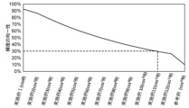
- FIG. 8A is a graph showing a light distribution pattern of light emitted from one light emitting area in Examples 1, 11 and Reference Example.
- FIG. 8B is a graph showing the uniformity of brightness of the second image in Examples 1 to 12 and the reference example.
- the video display devices according to Examples 1 to 12 and reference examples include a light source unit and a reflection unit, and the light source unit includes a plurality of light emitting areas arranged in a matrix and an imaging optical system. were set on the simulation software. Each light emitting area corresponds to each pixel 110p of the display device 110 in the above embodiment.
- the horizontal axis is the angle of the light emitting area with respect to the optical axis
- the vertical axis is the luminous intensity normalized by dividing the luminous intensity at that angle by the luminous intensity on the optical axis.
- the display device according to the first embodiment has an arrangement in which the luminous intensity of the light emitted from each light emitting area in the direction at an angle ⁇ with respect to the optical axis is expressed as cos ⁇ times the luminous intensity on the optical axis. It was set on the simulation software to have a light pattern. That is, in Example 1, the light emitted from each light emitting area has a strict Lambertian light distribution.
- the simulation software is set so that the luminous intensity in the direction of angle ⁇ with respect to the optical axis of each light emitting area has a light distribution pattern expressed as cos 20 ⁇ times the luminous intensity on the optical axis. did.
- the imaging optical systems in Examples 1 to 12 and Reference Example were all set to have telecentricity on the first image side.
- the brightness distribution of the second image formed when the brightness of all light emitting areas was kept constant was simulated.
- the second image was a rectangle with a long side of 111.2 mm and a short side of 27.8 mm.
- the plane on which the second image was formed was divided into square areas having sides of 1 mm, and the brightness value of each area was simulated.
- uniformity of brightness is a value expressed as a percentage of the minimum value to the maximum value of brightness within the second image.
- uniformity of brightness is a value expressed as a percentage of the minimum value to the maximum value of brightness within the second image.
- n in cos n ⁇ which is an approximate expression of the light distribution pattern, is preferably 11 or less, and even more preferably 1.
- the display brightness of the display device 110 is set to a predetermined value in advance. A brightness distribution can be provided.
- the display device 110 may be controlled so that the output of the LED element 112 of the pixel 110p on the outer edge side is larger than the output of the LED element 112 of the pixel 110p on the center side.
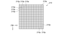
- FIG. 9 is a plan view showing the display device in this embodiment.
- FIG. 10A is a plan view showing the prism sheet in this embodiment.
- FIG. 10B is an end view taken along the line XB-XB shown in FIG. 10A.
- FIG. 11 is a plan view showing a display device and a prism sheet in this embodiment.
- pixels 210p are arranged in a matrix along the third direction (X direction) and the fourth direction (Y direction). That is, in the first embodiment, one pixel 110p is arranged in every four unit regions 110u, as shown in FIG. 2, but in this embodiment, a pixel 210p is arranged in every unit region. It is located.
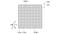
- the first prism sheet 230 of this embodiment has a first surface 230a into which light emitted from the display device 210 enters, and a second surface through which light is emitted toward the input element 121. 230b.
- a striped first prism 230p1 extending in the first direction is formed on the first surface 230a.
- No prism is formed on the second surface 230b, which is flat.
- the first direction is a direction inclined at 45 degrees with respect to the third direction.
- the arrangement direction of the first prisms 230p1 is defined as a second direction.
- the second direction is a direction inclined at 45 degrees with respect to the fourth direction.
- the third direction in which the pixels 210p of the display device 210 are arranged is the X direction
- the fourth direction in which the pixels 210p are arranged is the Y direction. It is.
- the first direction in which the first prisms 230p1 of the first prism sheet 230 extend is expressed as the V direction
- the second direction in which the plurality of first prisms 230p1 are arranged is expressed as the W direction.
- the angle between the V direction and the W direction is 90 degrees, and the V direction and the W direction are perpendicular to the Z direction.
- the X direction (third direction), Y direction (fourth direction), U direction (first direction), and V direction (second direction) are parallel to the second surface 230b of the first prism sheet 230. It is. Furthermore, as shown in FIG. 11, the arrangement period of the first prisms 230p1 is shorter than the arrangement period of the pixels 210p.
- FIG. 12A is a diagram showing a state in which some pixels 210p in the display device 210 are lit.
- FIG. 12B is a diagram showing pixels enlarged by the first prism 230p1.
- the display device 210 selectively lights up the pixels 210p.
- the display device 210 selectively lights up the pixels 210p.
- four pixels 210p are turned on, and the other pixels 210p are turned off.
- each pixel 210p when the light emitted from each pixel 210p enters the first prism 230p1 of the first prism sheet 230, this light is separated along the W direction.
- each pixel 210p when viewed from the viewer 14 side, each pixel 210p appears to be separated into two in the W direction.
- the two separated pixels 210p are not separated from each other and partially overlap.
- the area where the two pixels 210p overlap becomes relatively bright. Around this bright area, there is a relatively dark area in which only one pixel 210p is arranged. Thereby, the light emitted from each pixel 210p is diffused so as to have one peak along the W direction. As a result, the image displayed by the display device 210 becomes smooth.
- FIG. 13A is an end view showing the display device 210 and the first prism sheet 230 of this embodiment.
- FIG. 13B is an optical diagram showing the first prism 230p1 of this embodiment.
- FIG. 13C is an equation showing the relationship among the distance D, the prism angle ⁇ p, the refractive indices n0 and n1, and the pixel shift amount y.
- FIG. 13D is a graph showing the relationship between the distance D and the prism angle ⁇ p necessary to obtain the desired pixel shift amount y, with the horizontal axis representing the pixel shift amount y and the vertical axis representing the prism angle ⁇ p.
- the distance between the display device 210 and the first prism sheet 230 is D.
- Pa be the arrangement period (pixel pitch) of the pixels 210p in the display device 210.
- the arrangement period (prism pitch) of the first prisms 230p1 in the first prism sheet 230 is assumed to be P2.
- the angle between the surface of the first prism 230p1 and the second surface 230b is defined as a prism angle ⁇ p.
- the vertex angle of the first prism 230p1 is (180-2 ⁇ p) degrees.
- the prism angle ⁇ p is greater than 0 degrees and less than or equal to 45 degrees, preferably greater than or equal to 1 degree and less than or equal to 40 degrees. Therefore, the vertex angle of the first prism 230p1 is greater than or equal to 90 degrees and less than 180 degrees, preferably greater than or equal to 100 degrees and less than or equal to 178 degrees.
- the refractive index of the first prism sheet 230 is n1
- the refractive index of the environment in which the first prism sheet 230 is placed, for example, the atmosphere is n0
- the amount by which the pixel 210p is desired to be shifted is y. do.
- the distance D be short. However, if the distance D is made too short, the proportion of light that is totally reflected on the surface of the first prism 230p1 increases, and the light utilization efficiency decreases. In order to suppress total reflection, the prism angle ⁇ p may be made small, but if the prism angle ⁇ p is made small, it becomes difficult to obtain the pixel shift amount y. In other words, for the desired pixel shift amount y, there is a trade-off between shortening the distance D and reducing the prism angle ⁇ p.
- the pixel shift amount y can be expressed as a function of the distance D, the prism angle ⁇ p, and the refractive indexes n0 and n1 as shown in equation (1) shown in FIG. 13C.
- formula (1) When formula (1) is graphed with respect to several distances D and refractive indices n0 and n1, it becomes as shown in FIG. 13D.
- the pixel shift amount y in order to increase the pixel shift amount y, it is necessary to lengthen the distance D or increase the prism angle ⁇ p.
- the pixel pitch Pa is 0.1 mm and it is desired to shift the area irradiated with light by half of the pixel pitch Pa
- the pixel shift amount y will be 0.05 mm.
- the prism angle ⁇ p is about 4 degrees
- the prism angle ⁇ p is about 11 degrees.
- the ratio of prism pitch Pb to distance D is preferably 10% or less, more preferably 7.5% or less, more preferably 5% or less, and 2.5% or less. More preferred.
- FIG. 14A and 14B are diagrams showing the distribution of light transmitted through the first prism sheet 230, and FIG. 14A shows a case where the ratio of prism pitch Pb to distance D (Pb/D) is 1.5%, FIG. 14B shows the case where the ratio (Pb/D) is 5.0%.
- the first prism 230p1 separates the light emitted from each pixel 210p of the display device 210 into two pixels that partially overlap each other, thereby making it possible to make the image smooth.
- the configuration, operation, and effects of this embodiment other than those described above are the same as those of the first embodiment.
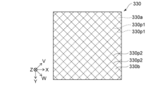
- FIG. 15 is a plan view showing the first prism sheet 330 of this embodiment. As shown in FIG. 15, in this embodiment, a first prism sheet 330 is provided in place of the first prism sheet 230 in the second embodiment.
- the first prism sheet 330 has a first surface 330a onto which light emitted from the display device 210 enters, and a second surface 330b from which light is emitted toward the input element 121.
- a striped first prism 330p1 extending in the first direction (V direction) is formed on the first surface 330a.
- a striped second prism 330p2 extending in the second direction (W direction) is formed on the second surface 330b.
- the first direction (V direction) is inclined at 45 degrees with respect to the third direction (X direction), and the second direction (W direction) is inclined at 45 degrees with respect to the fourth direction (Y direction). Therefore, the second direction (W direction) is perpendicular to the first direction (V direction).
- FIG. 16A is a diagram showing one pixel 210p in this embodiment.
- FIG. 16B is a diagram showing pixels enlarged by the first prism 330p1.
- FIG. 16C is a diagram showing pixels further enlarged by the second prism 330p2.
- FIG. 17A is a diagram showing an image displayed by the display device 210 in this embodiment.
- FIG. 17B is a diagram showing an image enlarged by the first prism 330p1.
- FIG. 17C is a diagram showing an image further enlarged by the second prism 330p2.
- FIG. 16A it is assumed that one pixel 210p of the display device 210 is lit.
- FIG. 16B when the light emitted from this pixel 210p enters the first prism 330p1, it is separated into two pixels 210p along the W direction. At this time, the two pixels 210p are separated so that they partially overlap. For example, two pixels 210p are shifted by 0.5 pixel.
- the two pixels 210p separated by the first prism 330p1 are each further separated into two pixels 210p along the V direction by the second prism 330p2, as shown in FIG. 16C.
- the pixel shift amount at this time is also such that the two pixels 210p partially overlap each other, for example, 0.5 pixel. Thereby, the light emitted from one pixel 210p is expanded to a region where four pixels 210p overlap.
- FIG. 17A it is assumed that the display device 210 displays an image G1.
- FIG. 17B the light emitted from the plurality of pixels 210p constituting this image G1 is separated by, for example, 0.5 pixels along the W direction by the first prism 330p1.
- an image G2 is synthesized in which two images G1 of the same shape are overlapped with each other with a shift of 0.5 pixel.
- the light separated by the first prism 330p1 is separated by, for example, 0.5 pixels along the V direction by the second prism 330p2.
- an image G3 is formed in which two images G2 of the same shape overlap each other with a shift of 0.5 pixel.
- Image G3 is an image in which four images G1 are overlapped.
- the image G1 displayed by the display device 210 passes through the first prism sheet 330 and becomes smooth.
- the first prism 330p1 is provided on the first surface 330a of the first prism sheet 330
- the second prism 330p2 is provided on the second surface, so that the image can be divided into two directions in the W direction and the V direction. separated along the directions. This makes the image smoother compared to the second embodiment.
- the configuration, operation, and effects of this embodiment other than those described above are the same as those of the second embodiment.
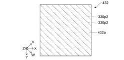
- FIG. 18A is a side view showing the display device 210, first prism sheet 431, and second prism sheet 432 of the light source unit according to this embodiment.
- FIG. 18B is a plan view showing the first prism sheet 431 of this embodiment.
- FIG. 18C is a plan view showing the second prism sheet 432 of this embodiment.
- this embodiment differs from the third embodiment in that the first prism 330p1 and the second prism 330p2 are arranged separately on two prism sheets. ing.
- the light source unit according to this embodiment is provided with a first prism sheet 431 and a second prism sheet 432, and the second prism sheet 432 is arranged between the first prism sheet 431 and the input element 121. .
- the first prism 330p1 is arranged on the first surface 431a of the first prism sheet 431, and the second prism 330p2 is arranged on the first surface 432a of the second prism sheet 432.
- the first prism 330p1 extends in a stripe shape in the first direction (V direction)
- the second prism 330p2 extends in a stripe shape in the second direction (W direction).
- the first surface 431a of the first prism sheet 431 and the first surface 432a of the second prism sheet 432 are surfaces facing the display device 210.
- first prism 330p1 may be arranged on the second surface 431b of the first prism sheet 431, and the second prism 330c2 may be arranged on the second surface 432b of the second prism sheet 432.
- the second surface 431b of the first prism sheet 431 and the second surface 432b of the second prism sheet 432 are surfaces facing the input element 121.
- the image displayed by the display device 210 can be made smooth, similar to the third embodiment.
- the configuration, operation, and effects of this embodiment other than those described above are the same as those of the third embodiment.
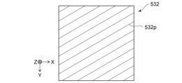
- FIG. 19 is a side view showing the display device 210, first prism sheet 531, second prism sheet 532, and third prism sheet 533 of the light source unit according to this embodiment.
- FIG. 20A is a plan view showing the first prism sheet 531 of this embodiment.
- FIG. 20B is a plan view showing the second prism sheet 532 of this embodiment.
- FIG. 20C is a plan view showing the third prism sheet 533 of this embodiment.
- the first prism sheet 531, the second prism sheet 532, and the third prism sheet 533 are arranged in this order along the direction from the display device 210 toward the input element 121.
- a first prism 531p is formed on the first prism sheet 531, a second prism 532p is formed on the second prism sheet 532, and a third prism 533p is formed on the third prism sheet 533. ing.
- the first prism 531p, the second prism 532p, and the third prism 533p are all striped and form an angle of 120 degrees with each other.
- each prism may be formed on any surface of each prism sheet. Further, two prisms may be formed on both sides of one prism sheet.
- 21A to 21D are schematic diagrams showing the operation of this embodiment.
- FIG. 21A it is assumed that one pixel 210p is lit.
- the light emitted from this pixel 210p is separated by the first prism 531p, and is separated into two pixels 210p.
- these two pixels 210p are each separated into two by the second prism 532p, and are separated into four pixels 210p.
- each of these four pixels 210p is further separated into two by the third prism 533p. However, at this time, since the two pixels 210p overlap at one location, there are ultimately seven pixels 210p. In this way, light emitted from one pixel 210p is separated into seven pixels 210p.
- the light emitted from the pixels can be expanded in three directions that form an angle of 120 degrees with each other, and the image can be made smoother.
- the configuration, operation, and effects of this embodiment other than those described above are the same as those of the fourth embodiment.
- FIG. 22 is a perspective view showing the first prism sheet of this embodiment.
- a first prism sheet 630 is provided.
- a first prism 630p is formed on the first prism sheet 630.
- the first prism 630p is not striped but has a convex shape, for example.
- a plurality of first prisms 630p are arranged in a matrix along a first direction (V direction) and a second direction (W direction).
- the first prism 630p has a pyramid shape (quadrangular pyramid shape).
- the shape of the first prism 630p is not limited to this, and may be, for example, a conical shape or a hexagonal pyramid shape.
- the first prism 630p may be a recessed portion.
- the arrangement direction of the first prisms 630p is not limited to the V direction and the W direction, but may be the same as the X direction and the Y direction, that is, the arrangement direction of the pixels of the display device.
- the configuration, operation, and effects of this embodiment other than those described above are the same as those of the third embodiment.
- FIG. 23 is an end view showing the video display device according to this embodiment.
- FIG. 24 is a schematic diagram showing the scenery seen from the viewer in the driver's seat in this embodiment.
- an automobile 1000 includes a vehicle 13 and a video display device 20 fixed to the vehicle 13.
- the video display device 20 includes a light source unit 11 and a reflection unit 22.
- the video display device 20 according to the present embodiment differs from the first embodiment in that the mirror surface 322a of the mirror 322 of the reflection unit 22 also serves as a reflection surface that allows the viewer 14 to view the second image IM2. This is different from the video display device 10.
- the configuration of the light source unit 11 in the video display device 20 is the same as that in the first embodiment.
- the light source unit 11 is arranged on the ceiling part 13b of the vehicle 13.
- the reflection unit 22 is arranged on the dashboard section 13c of the vehicle 13.
- Reflection unit 22 has a mirror 322.
- the mirror surface 322a of the mirror 322 is, for example, a concave surface.
- the mirror surface 322a is arranged at a position and at an angle facing the eye box 14a of the viewer 14 when the viewer 14 is in the driver's seat of the vehicle 13.
- the mirror surface 322a faces in a direction between the -X direction (rearward) and the +Z direction (upward).
- the angle of this mirror surface 322a can be finely adjusted depending on the position of the eyebox 14a of the viewer 14.
- the principal ray L emitted from the light source unit 11 travels in a direction between the +X direction (front) and the -Z direction (downward), is reflected at the mirror surface 322a of the mirror 322 of the reflection unit 22, and travels in the -X direction ( The light travels in a direction between the +Z direction (upward) and the +Z direction (upwards) and enters the eyebox 14a of the viewer 14.
- the path of the chief ray L from the light source unit 11 toward the reflection unit 12 is located inside the front windshield 13a of the vehicle 13, and generally follows the front windshield 13a.
- the chief ray L forms a first image IM1 at a position P between the light source unit 11 and the reflection unit 22. At this time, the first image IM1 becomes smooth due to the action of the first prism sheet 130.
- the viewer 14 can visually recognize the second image IM2, which is a virtual image, behind the mirror surface 322a of the dashboard portion 13c.
- the second image IM2 is formed far away from the mirror surface 322a, for example, 3 m ahead. Therefore, the viewer 14 can view the second image IM2 without significantly changing the focal length of his eyes from a state where he is viewing a distant scene through the front windshield 13a.
- the video display device 20 is divided into a light source unit 11 and a reflection unit 22, and is fixed at different positions in the vehicle 13, similarly to the first embodiment.
- the video display device 20 requires a long optical path length in order to form the second image IM2 at a position several meters in front of the vehicle. Part of the optical path length can be configured using the thirteen internal spaces. This eliminates the need to form the entire required optical path length inside the video display device 20, and the video display device 20 can be made smaller.
- the configuration of the reflection unit 22 can be simplified, and the reflection unit 22 can be made smaller.
- the viewer 14 can reliably view the second image IM2 without being affected by the background of the reflective surface.
- the configuration, operation, and effects of this embodiment other than those described above are the same as those of the first embodiment.
- the mirror 322 of the reflection unit 22 may be constituted by a half mirror or a transparent plate. Even in this case, by keeping the inside of the dashboard portion 13c dark, it is possible to prevent the viewer 14 from seeing the inside of the dashboard portion 13c.
- the mirror surface 322a of the mirror 322 may be black enough to sufficiently reflect the chief ray L emitted from the light source unit 11. Thereby, it is possible to suppress a decrease in visibility due to reflection of external light or the like by the mirror surface 322a of the mirror 322.
- the mirror 322 may be arranged continuously with the surface of the dashboard portion 13c. This eliminates the need to make a hole in the dashboard portion 13c, and improves the design of the interior of the automobile 1000.
- FIG. 25 is an end view showing the video display device according to this embodiment.
- FIG. 26 is an enlarged cross-sectional view of a part of the display device and reflective polarizing element shown in FIG. 25.
- a video display device 70A according to the present embodiment differs from the first embodiment in that it includes a display device 710A instead of the display device 110 and further includes a reflective polarizing element 740. This is different from the video display device 10.
- the display device 710A in this embodiment is different from the display device in the first embodiment in that the light exit surface of the LED element 712 is generally flat, and further includes a protective layer 714, a wavelength conversion member 715, and a light scattering member 716A. It is different from 110.
- the other configuration of the display device 710A is the same as the display device 110 in the first embodiment.
- the light source unit 71A according to the present embodiment includes the first prism sheet 130 similarly to the light source unit 11 according to the first embodiment. However, in FIG. 25, illustration of the first prism sheet 130 is omitted.
- the protective layer 714 covers the plurality of LED elements 712 arranged in rows and columns.
- the protective layer 714 is made of, for example, a polymer material having a sulfur (S)-containing substituent or a phosphorus (P) atom-containing group, or a high refractive material in which inorganic nanoparticles with a high refractive index are introduced into a polymer matrix such as polyimide.
- Transparent materials such as composite nanocomposite materials can be used.
- the wavelength conversion member 715 is arranged on the protective layer 714.
- the wavelength conversion member 715 includes one or more wavelength conversion materials such as a general phosphor material, a perovskite phosphor material, or a quantum dot (QD).
- the light emitted from each LED element 712 enters the wavelength conversion member 715.
- the wavelength conversion material emits light having an emission peak wavelength different from the emission peak wavelength of each LED element 712.
- the light emitted by the wavelength conversion member 715 has a substantially Lambertian light distribution.
- the light scattering member 716A includes, for example, a translucent resin member and light scattering particles or holes arranged in the resin member.
- the resin member include polycarbonate.
- light-scattering particles include materials that have a refractive index difference with the resin member, such as titanium oxide. Note that the light scattering member 716A may obtain a light scattering effect by roughening its surface to provide unevenness.
- the reflective polarizing element 740 for example, a multilayer thin film laminated polarizing plate in which thin film layers having different polarization characteristics are laminated can be used.
- Reflective polarizing element 740 is placed on display device 710A.
- the reflective polarizing element 740 is placed on the light scattering member 716A. Therefore, the light emitted from the LED element 712 and the wavelength conversion member 715 enters the reflective polarizing element 740.
- the reflective polarizing element 740 transmits the first polarized light 710p of the light emitted from the display device 710A, and reflects the second polarized light 710s toward the display device 710A.
- the direction of vibration of the electric field of the second polarized light 710s is approximately orthogonal to the direction of vibration of the electric field of the first polarized light 710p.
- the first polarized light 710p is P polarized light
- the second polarized light 710s is S polarized light
- P-polarized light means light whose electric field vibration direction is substantially parallel to the XY plane
- S-polarized light means light whose electric field vibration direction is approximately perpendicular to the XY plane including incident light and reflected light.
- the viewer 14 driving the vehicle 13 may wear polarized sunglasses 14b in order to reduce the glare of sunlight that is reflected from a puddle in front of the vehicle 13 and transmitted through the front windshield 13a.
- the component corresponding to P-polarized light when viewed from the front windshield 13a is particularly reduced in sunlight reflected by a puddle or the like, so the polarized sunglasses 14b blocks most of the S-polarized light.
- the polarized sunglasses 14b blocks most of the S-polarized light.
- most of the S-polarized light included in the light emitted by the display device 710A is also blocked by the polarized sunglasses 14b, so that the viewer 14 cannot visually recognize the second image IM2. It may become difficult.
- P-polarized light and S-polarized light in this specification are physically defined by the presence of a reflective object such as the above-mentioned puddle.
- the reflective polarizing element 740 transmits the first polarized light 710p of the light emitted from the display device 710A and reflects the second polarized light 710s. Most of the first polarized light 710p transmitted through the reflective polarizing element 740 passes through the imaging optical system 120, the reflective unit 12, and the inner surface of the front windshield 13a, and then passes through the eye box without being blocked by the polarized sunglasses 14b. 14a. Note that the incident angle of the first polarized light 710p when it enters the inner surface of the front windshield 13a is set to be an angle different from the Brewster angle.
- the light emitted from the LED element 712 is irradiated onto the wavelength conversion member 715.
- the wavelength conversion member 715 is excited and emits light having a peak emission wavelength longer than the peak emission wavelength of the light emitted from the LED element 712.
- the light emitted from the display device 710A includes light emitted from the LED element 712 and light emitted from the wavelength conversion member 715.
- the light emitted from the LED element 712 is also referred to as "short wavelength light”
- the light emitted from the wavelength conversion member 715 is also referred to as "long wavelength light”.
- most of the light emitted from the LED element 712 may be absorbed by the wavelength conversion member 715.
- Most of the first polarized light 710p included in these short wavelength lights and long wavelength lights passes through the reflective polarizing element 740 and exits from the imaging optical system 120. Furthermore, most of the second polarized light 710s included in these short wavelength lights and long wavelength lights is reflected by the reflective polarizing element 740. A portion of the second polarized light 710s reflected by the reflective polarizing element 740 is scattered and reflected by components of the display device 710A, such as the light scattering member 716A and the wavelength conversion member 715. Due to scattered reflection, a portion of the second polarized light 710s is converted into the first polarized light 710p.
- a part of the first polarized light 710p converted from the second polarized light 710s passes through the reflective polarizing element 740 and is emitted from the light source unit 71A. Therefore, the brightness of the first image IM1 can be improved while increasing the proportion of the first polarized light 710p included in the light emitted from the light source unit 71A.
- the brightness of the second image IM2 also improves. This makes it easier for the viewer 14 to visually recognize the second image IM2.
- a part of the short wavelength light included in the second polarized light 710s may be reflected by the reflective polarizing element 740 and then enter the wavelength conversion member 715.
- the wavelength conversion member 715 absorbs the short wavelength light of the second polarized light 710s and newly emits long wavelength light. Both the scattered reflected light and the emitted light have approximately Lambertian light distribution.
- the reflective polarizing element 740 itself may scatter and reflect the second polarized light 710s. Also in this case, a part of the second polarized light 710s is converted into the first polarized light 710p due to scattering and reflection.
- one reflective polarizing element 740 covers all pixels of the display device 710A.
- the light source unit may include a plurality of reflective polarizing elements, and each reflective polarizing element may be arranged on each pixel.
- the configuration of the display device used in combination with the reflective polarizing element is not limited to the above.
- the display device may be configured without the light scattering member.
- the display device may be configured without the wavelength conversion member.
- the display device can be converted into a wavelength converting member and a light scattering member.
- a configuration in which neither is provided may be used.
- the light source unit 71A is arranged on the display device 710A, transmits the first polarized light 710p of the light emitted from the display device 710A, and transmits the second polarized light 710s of the light emitted from the display device 710A. It further includes a reflective polarizing element 740 that reflects. Therefore, the brightness of the first image IM1 can be improved while increasing the proportion of the first polarized light 710p included in the light emitted from the light source unit 71A.
- the light emitted from the reflective polarizing element 740 also has a substantially Lambertian light distribution. Therefore, also in this embodiment, it is possible to provide the light source unit 71A that can form the first image IM1 that is small and of high quality. Note that since the plurality of LED elements 712 are discretely mounted on the substrate 111, a grainy appearance may occur in the first image IM1.
- the wavelength conversion member 715 has the effect of alleviating this graininess.
- the light scattering member 716A can further enhance the effect of alleviating this graininess.
- the configuration, operation, and effects of this embodiment other than those described above are the same as those of the first embodiment.
- FIG. 27 is a side view showing the light source unit according to this embodiment.
- a light source unit 71B includes a display device 710A having a configuration similar to that of the eighth embodiment instead of the display device 110, and a reflective polarizing element 750.
- the video display device 10 is different from the video display device 10 according to the first embodiment in that it further includes a light shielding member 760. Note that in FIG. 27, only the light shielding member 760 is shown in cross section.
- the reflective polarizing element 750 for example, a wire grid type reflective polarizing element using a plurality of metal nanowires can be used.
- the reflective polarizing element 750 is arranged in a portion of the optical path from the display device 710A to the reflective unit 12, where the plurality of principal rays L are substantially parallel to each other.
- the plurality of principal rays L are substantially parallel to each other in the optical path between the intermediate element 122 and the reflection unit 12, and the reflective polarizing element 750 is arranged between the intermediate element 122 and the output element 123. be done.
- the reflective polarizing element 750 transmits the first polarized light 710p, which is P-polarized light, and reflects the second polarized light 710s, which is S-polarized light, back to the display device 710A. Specifically, light 710a including first polarized light 710p and second polarized light 710s is emitted from display device 710A. This light 710a enters the reflective polarizing element 750 after passing through the input element 121 and the intermediate element 122.
- the reflective polarizing element 750 transmits most of the first polarized light 710p included in this light 710a. Most of the first polarized light 710p that has passed through the reflective polarizing element 750 is output from the reflective unit 12 after passing through the output element 123.
- the reflective polarizing element 750 reflects most of the second polarized light 710s included in this light 710a so as to return along the optical path from the display device 710A to the reflective polarizing element 750.
- the shape of the reflective polarizing element 750 is a flat plate.
- the reflective polarizing element 750 is arranged so as to be substantially perpendicular to the principal ray L.
- the reflective polarizing element 750 specularly reflects most of the second polarized light 710s. Therefore, most of the second polarized light 710s reflected by the reflective polarizing element 750 passes through the intermediate element 122 and the input element 121 in this order, and then returns to the display device 710A.
- a part of the second polarized light 710s that has returned to the display device 710A is scattered and reflected by components of the display device 710A, such as the light scattering member 716A and the wavelength conversion member 715. Due to scattered reflection, a portion of the second polarized light 710s is converted into the first polarized light 710p.
- a part of the first polarized light 710p converted from the second polarized light 710s passes through the reflective polarizing element 750 after passing through the input element 121 and the intermediate element 122. Most of the first polarized light 710p that has passed through the reflective polarizing element 750 is output from the reflective unit 12 after passing through the output element 123. Therefore, the brightness of the second image IM2 can be improved while increasing the proportion of the first polarized light 710p included in the light emitted from the video display device 70B. This makes it easier for the viewer 14 to visually recognize the second image IM2.
- a portion of the short wavelength light included in the second polarized light 710s returned to the display device 710A may be irradiated onto the wavelength conversion member 715, as in the eighth embodiment.
- the effect can be expected that the wavelength conversion member 715 absorbs the short wavelength light of the second polarized light 710s and newly emits long wavelength light.
- the light shielding member 760 is arranged between the display device 710A and the input element 121 of the imaging optical system 120.
- the shape of the light shielding member 760 is, for example, a flat plate substantially parallel to the XY plane.
- the light shielding member 760 is provided with an opening 761 that penetrates the light shielding member 760 in the Z direction.
- the focal point F of the imaging optical system 120 is located within the aperture 761.
- the light that passes through the focal point F and its vicinity passes through the opening 761 of the light shielding member 760 and enters the input element 121, and most of the other light passes through the light shielding member 760. is blocked by.
- the light along the optical path that is, the light passing through the focal point F and its vicinity, passes through the opening 761 of the light shielding member 760 and returns to the display device 710A.
- most of the second polarized light 710s reflected by the reflective polarizing element 750 which does not go along the optical path but goes toward the display device 710A, is blocked by the light shielding member 760.
- the video display device 70B further includes a reflective polarizing element 750.
- the reflective polarizing element 750 is configured so that, in the optical path from the display device 710A to the reflection unit 12, a plurality of chief rays L that are emitted from different positions in the display device 710A and pass through the first image IM1 are substantially parallel to each other.
- the first polarized light 710p of the light emitted from the display device 710A is transmitted therethrough, and the second polarized light 710s of the light emitted from the display device 710A is reflected back to the display device 710A. Therefore, the brightness of the second image IM2 can be improved while increasing the proportion of the first polarized light 710p included in the light emitted from the video display device 70B.
- a light shielding member 760 is provided between the display device 710A and the input element 121.
- the light shielding member 760 is provided with an opening 761 through which the second polarized light 710s returning to the display device 710A along the optical path passes. Therefore, while allowing the light along the optical path of the second polarized light 710s reflected by the reflective polarizing element 750 to return to the display device 710A, the light along the optical path of the second polarized light 710s reflected by the reflective polarizing element 750 is allowed to return to the display device 710A. Stray light that does not follow the direction can be suppressed from heading toward the display device 710A.
- the quality of the first image IM1 and the second image IM2 can be improved.
- the light shielding member 760 due to the light shielding member 760, stray light out of the light emitted from the display device 710A that does not follow the optical path is reflected by the reflective polarizing element 750 and the optical elements of the imaging optical system 120, and heads toward the display device 710A. It is possible to suppress re-excitation and scattering reflection in places where it is not possible.
- the light shielding member 760 may not be provided in the video display device 70B.
- the reflective polarizing element 740 described in the eighth embodiment may be further provided on the display device 710A of the video display device 70B.
- the second polarized light 710s that was not completely reflected by the reflective polarizing element 740 on the display device 710A can be reflected by the reflective polarizing element 750. Therefore, the brightness of the second image IM2 can be improved while increasing the proportion of the first polarized light 710p included in the light emitted from the video display device 70B.
- the configuration, operation, and effects of this embodiment other than those described above are the same as those of the eighth embodiment.
- FIG. 28 is a side view showing a light source unit according to this modification. Also in FIG. 28, only the light shielding member 760 is shown in cross section.
- a reflective polarizing element 750 is arranged between the output element 123 and the reflective unit 12. Note that although FIG. 28 shows an example in which the reflective polarizing element 750 is located between the output element 123 and the first image IM1, the reflective polarizing element 570 is positioned between the first image IM1 and the reflective unit 12. may be placed between.
- the configuration, operation, and effects of this modification other than those described above are the same as those of the ninth embodiment.
- the embodiment includes the following aspects.
- a display device capable of displaying images; a first prism sheet into which light emitted from the display device is incident; an input element into which light emitted from the first prism sheet is incident; and an output element into which light that has passed through the input element is incident; the light emitted from the output element forms a first image corresponding to the image; an imaging optical system that forms a Equipped with The imaging optical system has substantially telecentricity on the first image side, A light source unit in which light emitted from the display device has a substantially Lambertian light distribution.
- the first prism sheet has a first surface onto which light emitted from the display device enters, and a second surface that emits light toward the input element, A striped first prism extending in a first direction is formed on the first surface,
- the display device has a plurality of pixels arranged along a third direction and a fourth direction orthogonal to the third direction, The first direction is inclined at 45 degrees with respect to the third direction, The light source unit according to appendix 2, wherein the second direction is inclined at 45 degrees with respect to the fourth direction.
- the display device has a plurality of pixels arranged along a third direction and a fourth direction orthogonal to the third direction, The first direction is inclined at 45 degrees with respect to the third direction, The light source unit according to appendix 4, wherein the second direction is inclined at 45 degrees with respect to the fourth direction.
- the light emitted from the display device has a light distribution pattern in which the luminous intensity in a direction at an angle ⁇ with respect to the optical axis of the light emitted from the display device is approximated by cos n ⁇ times the luminous intensity on the optical axis.
- the light source unit according to any one of Supplementary notes 1 to 5, wherein the n is a value larger than 0.
- Appendix 7 The light source unit according to appendix 6, wherein n is 11 or less.
- Appendix 8 The light source unit according to any one of appendices 1 to 7, wherein the display device is an LED display having a plurality of LED elements.
- Appendix 10 The light source unit according to appendix 8 or 9, wherein the display device further includes a wavelength conversion member that is disposed on the LED element and into which light emitted from the LED element enters.
- the imaging optical system includes a bending section including the input element, and a direction changing section including the output element,
- the bending portion is configured such that a plurality of chief rays exit from different positions in the display device and cross each other to reach the first image before entering the input element, before and after the first image. bending the plurality of chief rays so that they become substantially parallel; Any one of Supplementary Notes 1 to 10, wherein the direction changing unit changes the traveling direction of the plurality of chief rays so that the plurality of chief rays that have passed through the bending part head toward the formation position of the first image.
- An opening is provided between the display device and the imaging optical system, through which a portion of light directed from the display device to the imaging optical system passes, and is directed from the display device to the imaging optical system.
- the light source unit according to any one of Supplementary Notes 1 to 10, further comprising a light shielding member that blocks another part of the light.
- a light source unit according to any one of Supplementary Notes 1 to 12, a reflection unit that is separated from the light source unit and reflects the light emitted from the imaging optical system; Equipped with The first image is an image display device formed between the light source unit and the reflection unit.
- the display device is arranged on an optical path from the display device to the reflection unit, transmits the first polarized light of the light emitted from the display device, and transmits the second polarized light of the light emitted from the display device to the display device.
- the video display device according to appendix 13 further comprising a reflective polarizing element that reflects light back to .
- the present invention can be used, for example, in a head-up display.
- Video display device 11 Light source unit 12: Reflection unit 13: Vehicle 13a: Front windshield 13b: Ceiling section 13c: Dashboard section 13h1: Through hole 13h2: Through hole 13s1: Wall 13s2: Wall 14: Viewer 14a: Eye box 14b: Polarized sunglasses 15: Wavelength conversion member 20: Image display device 22: Reflection units 70A, 70B: Image display devices 71A, 71B: Light source unit 110: Display device 110p: Pixel 110u: Unit area 111: Substrate 112: LED Element 112a: Semiconductor stack 112b: Anode electrode 112c: Cathode electrode 112p1: P-type semiconductor layer 112p2: Active layer 112p3: N-type semiconductor layer 112s: Light exit surface 112t: Recesses 118a, 118b: Wiring 120: Imaging optical system 120a :Bending part 120b:Direction changing part 121:Input element 121a:Mirror surface 122Intermediate element 122
Abstract
This light source unit comprises a display device capable of displaying an image, a first prism sheet on which light emitted from the display device is incident, and an image formation optical system. The image formation optical system includes an input element on which light emitted from the first prism sheet is incident and an output element on which light that has gone through the input element is incident, and light emitted from the output element forms a first image corresponding to the image. The image formation optical system has an approximately telecentric property on the first image side. The light emitted from the display device has an approximately Lambertian light distribution.
Description
実施形態は、光源ユニット及び映像表示装置に関する。
Embodiments relate to a light source unit and an image display device.
特許文献1には、画像を表示可能な表示装置から出射した光を、複数のミラーで順次反射し、最後のミラーにおいて反射された光を、ウインドシールド等の反射部材で使用者に向けてさらに反射し、使用者に表示装置が表示する画像に応じた虚像を視認させる技術が開示されている。このような装置は、小型化が要望されている。
Patent Document 1 discloses that light emitted from a display device capable of displaying an image is sequentially reflected by a plurality of mirrors, and the light reflected by the last mirror is further directed toward the user by a reflective member such as a windshield. A technique is disclosed in which a virtual image is reflected and allows a user to view a virtual image corresponding to an image displayed by a display device. There is a demand for miniaturization of such devices.
本発明の実施形態は、上述の問題点に鑑みてなされたものであって、小型化が可能な光源ユニット及び映像表示装置を提供することを目的とする。
The embodiments of the present invention have been made in view of the above-mentioned problems, and an object thereof is to provide a light source unit and an image display device that can be downsized.
本発明の実施形態に係る光源ユニットは、画像を表示可能な表示装置と、前記表示装置から出射した光が入射する第1プリズムシートと、結像光学系と、を備える。前記結像光学系は、前記第1プリズムシートから出射した光が入射する入力素子と、前記入力素子を経由した光が入射する出力素子と、を含み、前記出力素子から出射した光が前記画像に応じた第1の像を形成する。前記結像光学系は、前記第1の像側において略テレセントリック性を有する。前記表示装置から出射する光は略ランバーシアン配光を有する。
A light source unit according to an embodiment of the present invention includes a display device capable of displaying an image, a first prism sheet into which light emitted from the display device enters, and an imaging optical system. The imaging optical system includes an input element into which the light emitted from the first prism sheet enters, and an output element into which the light that has passed through the input element enters, and the light emitted from the output element forms the image. A first image is formed according to the image. The imaging optical system has substantially telecentricity on the first image side. The light emitted from the display device has a substantially Lambertian light distribution.
本発明の実施形態に係る映像表示装置は、前記光源ユニットと、前記光源ユニットから離隔し、前記結像光学系から出射した光を反射する反射ユニットと、を備える。前記第1の像は、前記光源ユニットと前記反射ユニットとの間に形成される。
An image display device according to an embodiment of the present invention includes the light source unit and a reflection unit that is spaced apart from the light source unit and reflects light emitted from the imaging optical system. The first image is formed between the light source unit and the reflection unit.
実施形態によれば、小型化が可能な光源ユニット及び映像表示装置を実現できる。
According to the embodiment, it is possible to realize a light source unit and an image display device that can be downsized.
以下に、各実施形態及びその変形例について図面を参照しつつ説明する。なお、図面は模式的または概念的なものであり、適宜強調又は簡略化されている。例えば、各部分の厚みと幅との関係、部分間の大きさの比率などは、必ずしも現実のものと同一とは限らない。また、同じ部分を表す場合であっても、図面により互いの寸法や比率が異なって表される場合もある。さらに、本明細書と各図において、既出の図に関して説明したものと同様の要素には同一の符号を付して詳細な説明は適宜省略する。
Each embodiment and its modification examples will be described below with reference to the drawings. Note that the drawings are schematic or conceptual, and are emphasized or simplified as appropriate. For example, the relationship between the thickness and width of each part, the size ratio between parts, etc. are not necessarily the same as those in reality. Furthermore, even when the same part is shown, the dimensions and ratios may be shown differently depending on the drawing. Furthermore, in this specification and each figure, the same elements as those described in relation to the previous figures are given the same reference numerals, and detailed explanations are omitted as appropriate.
<第1の実施形態>
先ず、第1の実施形態について説明する。
図1は、本実施形態に係る映像表示装置を示す端面図である。
図2は、本実施形態に係る光源ユニットの表示装置を示す平面図である。
図3Aは、本実施形態に係る光源ユニットの第1プリズムシートを示す斜視図である。
図3B及び図3Cは、本実施形態に係る光源ユニットの第1プリズムシートを示す端面図である。 <First embodiment>
First, a first embodiment will be described.
FIG. 1 is an end view showing a video display device according to this embodiment.
FIG. 2 is a plan view showing the display device of the light source unit according to this embodiment.
FIG. 3A is a perspective view showing the first prism sheet of the light source unit according to this embodiment.
3B and 3C are end views showing the first prism sheet of the light source unit according to this embodiment.
図1に示すように、本実施形態に係る映像表示装置10は、光源ユニット11と、反射ユニット12と、を備える。光源ユニット11は、表示装置110と、結像光学系120と、第1プリズムシート130と、を有する。表示装置110は複数の画素を有し、画像を表示可能である。第1プリズムシート130には、表示装置110から出射した光が入射する。結像光学系120は、第1プリズムシート130から出射した光が入射し、表示装置110が表示した画像に応じた第1の像IM1を形成する。第1の像IM1は、実像であって中間像である。反射ユニット12は、光源ユニット11から離隔し、結像光学系120から出射した光を反射する。
As shown in FIG. 1, the video display device 10 according to the present embodiment includes a light source unit 11 and a reflection unit 12. The light source unit 11 includes a display device 110, an imaging optical system 120, and a first prism sheet 130. The display device 110 has a plurality of pixels and can display images. Light emitted from the display device 110 enters the first prism sheet 130 . The imaging optical system 120 receives the light emitted from the first prism sheet 130 and forms a first image IM1 corresponding to the image displayed by the display device 110. The first image IM1 is a real image and an intermediate image. The reflection unit 12 is spaced apart from the light source unit 11 and reflects the light emitted from the imaging optical system 120.
映像表示装置10は、例えば自動車1000に搭載されて、HUD(Head Up Display)を構成する。自動車1000は、車両13と、車両13に固定された映像表示装置10と、を備える。視認者14は自動車1000の搭乗者であり、例えば、運転者である。
The video display device 10 is mounted on, for example, a car 1000 and constitutes a HUD (Head Up Display). The automobile 1000 includes a vehicle 13 and a video display device 10 fixed to the vehicle 13. The viewer 14 is a passenger of the automobile 1000, for example, a driver.
光源ユニット11の表示装置110は、HUDにより視認者14に視認させたい画像を表示する。第1プリズムシート130は、表示装置110の各画素から出射した光を屈折させて、各画素から出射した光が到達する領域を拡大する。このメカニズムについては後述する。結像光学系120は、第1プリズムシート130から出射した光を反射ユニット12に対して出力すると共に、光源ユニット11と反射ユニット12との間に第1の像IM1を結像する。反射ユニット12は光源ユニット11から出射した光を車両13のフロントウインドシールド13aに向けて反射する。フロントウインドシールド13aは、例えば、ガラスを含む。
The display device 110 of the light source unit 11 displays an image that is desired to be viewed by the viewer 14 using the HUD. The first prism sheet 130 refracts the light emitted from each pixel of the display device 110 and expands the area where the light emitted from each pixel reaches. This mechanism will be described later. The imaging optical system 120 outputs the light emitted from the first prism sheet 130 to the reflection unit 12, and forms a first image IM1 between the light source unit 11 and the reflection unit 12. The reflection unit 12 reflects the light emitted from the light source unit 11 toward the front windshield 13a of the vehicle 13. The front windshield 13a includes, for example, glass.
フロントウインドシールド13aは、その内面において、反射ユニット12から到達した光を反射し、視認者14のアイボックス14aに入射させる。これにより、視認者14は、フロントウインドシールド13aの向こう側に、表示装置110が表示する画像に応じた第2の像IM2を視認できる。第2の像IM2は、第1の像IM1よりも大きい虚像である。「アイボックス」とは、視認者の眼の前の空間のうち、虚像が視認可能な範囲をいう。
The front windshield 13a reflects the light arriving from the reflection unit 12 on its inner surface and makes it enter the eyebox 14a of the viewer 14. Thereby, the viewer 14 can visually recognize the second image IM2 corresponding to the image displayed by the display device 110 on the other side of the front windshield 13a. The second image IM2 is a virtual image larger than the first image IM1. The "eye box" refers to the area in front of the viewer's eyes where a virtual image can be viewed.
以下、説明をわかりやすくするために、XYZ直交座標系を用いて、各部分の配置および構成を説明する。本実施形態では、車両13の前後方向を「X方向」とし、車両13の左右方向を「Y方向」とし、車両13の上下方向を「Z方向」とする。XY平面は、車両13の水平面である。X方向のうち矢印の方向(前方)を「+X方向」といい、その逆方向(後方)を「-X方向」ともいう。また、Y方向のうち矢印の方向(左方)を「+Y方向」といい、その逆方向(右方)を「-Y方向」ともいう。また、Z方向のうち矢印の方向(上方)を「+Z方向」といい、その逆方向(下方)を「-Z方向」ともいう。
Hereinafter, in order to make the explanation easier to understand, the arrangement and configuration of each part will be explained using an XYZ orthogonal coordinate system. In this embodiment, the longitudinal direction of the vehicle 13 is referred to as the "X direction," the left-right direction of the vehicle 13 is referred to as the "Y direction," and the vertical direction of the vehicle 13 is referred to as the "Z direction." The XY plane is a horizontal plane of the vehicle 13. Of the X directions, the direction of the arrow (forward) is called the "+X direction", and the opposite direction (backward) is also called the "-X direction". Further, in the Y direction, the direction of the arrow (to the left) is referred to as the "+Y direction", and the opposite direction (to the right) is also referred to as the "-Y direction". Further, in the Z direction, the direction of the arrow (upward) is referred to as the "+Z direction", and the opposite direction (downward) is also referred to as the "-Z direction".
また、図1においては、第1の像IM1が形成される位置を円形のマークにより示している。第1の像IM1と同様に、第2の像IM2が形成される位置も円形のマークにより示している。一方、表示装置110において第1の像IM1の各マークに到達する主光線Lが出射する位置を、四角形のマークにより示している。このように、説明をわかりやすくするために、各主光線Lにおいて表示装置110上の出射位置を、第1の像IM1の結像位置と第2の像IM2の結像位置とは別のマークで示しているが、表示装置110上に表示される画像と第1の像IM1と第2の像IM2とは、概ね相似関係にある。
Furthermore, in FIG. 1, the position where the first image IM1 is formed is indicated by a circular mark. Similar to the first image IM1, the position where the second image IM2 is formed is also indicated by a circular mark. On the other hand, in the display device 110, the positions from which the principal ray L that reaches each mark of the first image IM1 is emitted are indicated by square marks. In this way, in order to make the explanation easier to understand, the emission position of each principal ray L on the display device 110 is set to a different mark from the imaging position of the first image IM1 and the imaging position of the second image IM2. As shown in , the image displayed on the display device 110, the first image IM1, and the second image IM2 have a generally similar relationship.
図2に示すように、表示装置110には、第3方向及び第4方向に沿った単位領域110uが行列状に配列されており、第3方向及び第4方向について、1つおきの単位領域110uに画素110pが配置されている。これにより、2行2列の4つの単位領域110u毎に1つの画素110pが配置されている。このように、表示装置110においては、複数の画素110pが第3方向と第4方向に沿って千鳥状に配列されている。
As shown in FIG. 2, in the display device 110, unit areas 110u are arranged in a matrix along the third direction and the fourth direction, and every other unit area 110u is arranged in the third direction and the fourth direction. A pixel 110p is arranged at 110u. As a result, one pixel 110p is arranged for every four unit areas 110u arranged in 2 rows and 2 columns. In this way, in the display device 110, the plurality of pixels 110p are arranged in a staggered manner along the third direction and the fourth direction.
第4方向は第3方向に対して交差、例えば、直交する。例えば、第3方向は画像の水平方向であり、第4方向は画像の垂直方向である。本実施形態においては、第3方向をX方向とし、第4方向をY方向とする。表示装置110から出射する光は略ランバーシアン配光を有する。表示装置110の具体的な構成及びランバーシアン配光については、後に詳しく説明する。
The fourth direction intersects, for example, is orthogonal to the third direction. For example, the third direction is the horizontal direction of the image, and the fourth direction is the vertical direction of the image. In this embodiment, the third direction is the X direction, and the fourth direction is the Y direction. The light emitted from the display device 110 has a substantially Lambertian light distribution. The specific configuration of the display device 110 and the Lambertian light distribution will be described in detail later.
図3A~図3Cに示すように、第1プリズムシート130は、表示装置110から出射した光が入射する第1面130aと、第1面130aの反対側の第2面130bと、を有する。第2面130bは結像光学系120に向けて光を出射する。第1プリズムシート130の第1面130aには、第4方向(Y方向)に延びるストライプ状の第1プリズム130p1が形成されており、第2面130bには、第3方向(X方向)に延びるストライプ状の第2プリズム130p2が形成されている。
As shown in FIGS. 3A to 3C, the first prism sheet 130 has a first surface 130a onto which light emitted from the display device 110 enters, and a second surface 130b opposite to the first surface 130a. The second surface 130b emits light toward the imaging optical system 120. A striped first prism 130p1 extending in the fourth direction (Y direction) is formed on the first surface 130a of the first prism sheet 130, and a striped first prism 130p1 extending in the third direction (X direction) is formed on the second surface 130b. An extending stripe-shaped second prism 130p2 is formed.
-Z方向から見て、第1プリズムシート130は表示装置110と同じ又は表示装置110よりも大きく、表示装置110を覆っている。また、X方向における第1プリズム130p1の配列周期は、X方向における表示装置110の単位領域110uの配列周期よりも短い。同様に、Y方向における第2プリズム130p2の配列周期は、Y方向における単位領域110uの配列周期よりも短い。これにより、表示装置110の各画素110pから出射した光は、必ず1つ以上の第1プリズム130p1及び1つ以上の第2プリズム130p2に入射する。
When viewed from the −Z direction, the first prism sheet 130 is the same as or larger than the display device 110 and covers the display device 110. Furthermore, the arrangement period of the first prisms 130p1 in the X direction is shorter than the arrangement period of the unit area 110u of the display device 110 in the X direction. Similarly, the arrangement period of the second prisms 130p2 in the Y direction is shorter than the arrangement period of the unit regions 110u in the Y direction. Thereby, the light emitted from each pixel 110p of the display device 110 always enters one or more first prisms 130p1 and one or more second prisms 130p2.
次に、映像表示装置10における上記以外の構成を説明する。
先ず、表示装置110について説明する。
図4は、本実施形態に係る映像表示装置の表示装置を示す端面図である。 Next, the configuration of thevideo display device 10 other than the above will be explained.
First, thedisplay device 110 will be explained.
FIG. 4 is an end view showing the display device of the video display device according to this embodiment.
先ず、表示装置110について説明する。
図4は、本実施形態に係る映像表示装置の表示装置を示す端面図である。 Next, the configuration of the
First, the
FIG. 4 is an end view showing the display device of the video display device according to this embodiment.
光源ユニット11の表示装置110はLEDディスプレイである。表示装置110においては、複数のLED素子112が千鳥状に配列されている。表示装置110の各画素110pには、1つ又は複数のLED素子112が配置されている。
The display device 110 of the light source unit 11 is an LED display. In the display device 110, a plurality of LED elements 112 are arranged in a staggered manner. One or more LED elements 112 are arranged in each pixel 110p of the display device 110.
図4に示すように、表示装置110において、各LED素子112は、基板111にフェースダウン実装されている。ただし、各LED素子は、基板にフェースアップ実装されてもよい。各LED素子112は、半導体積層体112aと、アノード電極112bと、カソード電極112cと、を有する。基板111には、樹脂やガラスのような絶縁材料が用いられる。また、基板111には、各LED素子112を駆動するためのシリコン半導体チップを用いることもできる。
As shown in FIG. 4, in the display device 110, each LED element 112 is mounted face down on the substrate 111. However, each LED element may be mounted face-up on the board. Each LED element 112 has a semiconductor stack 112a, an anode electrode 112b, and a cathode electrode 112c. The substrate 111 is made of an insulating material such as resin or glass. Moreover, a silicon semiconductor chip for driving each LED element 112 can also be used for the substrate 111.
半導体積層体112aは、p型半導体層112p1と、p型半導体層112p1上に配置される活性層112p2と、活性層112p2上に配置されるn型半導体層112p3と、を有する。半導体積層体112aには、例えばInXAlYGa1-X-YN(0≦X、0≦Y、X+Y<1)で表せる窒化ガリウム系化合物半導体が用いられる。LED素子112が発光する光は、本実施形態では可視光である。
The semiconductor stack 112a includes a p-type semiconductor layer 112p1, an active layer 112p2 placed on the p-type semiconductor layer 112p1, and an n-type semiconductor layer 112p3 placed on the active layer 112p2. For example, a gallium nitride-based compound semiconductor represented by In X Al Y Ga 1-XY N (0≦X, 0≦Y, X+Y<1) is used for the semiconductor stack 112a. The light emitted by the LED element 112 is visible light in this embodiment.
アノード電極112bは、p型半導体層112p1に電気的に接続される。また、アノード電極112bは、配線118bに電気的に接続される。カソード電極112cは、n型半導体層112p3に電気的に接続される。また、カソード電極112cは、別の配線118aに電気的に接続される。各電極112b、112cには、例えば金属材料を用いることができる。
The anode electrode 112b is electrically connected to the p-type semiconductor layer 112p1. Further, the anode electrode 112b is electrically connected to the wiring 118b. The cathode electrode 112c is electrically connected to the n-type semiconductor layer 112p3. Further, the cathode electrode 112c is electrically connected to another wiring 118a. For example, a metal material can be used for each electrode 112b, 112c.
本実施形態では各LED素子112の光出射面112sには、複数の凹部112tが設けられている。本明細書において「LED素子の光出射面」とは、LED素子の表面のうち、結像光学系120に入射する光が主に出射する面を意味する。本実施形態では、n型半導体層112p3において、活性層112p2と対向する面の反対側に位置する面が、光出射面112sに相当する。
In this embodiment, a plurality of recesses 112t are provided on the light exit surface 112s of each LED element 112. In this specification, the term "light exit surface of the LED element" refers to the surface of the LED element from which the light incident on the imaging optical system 120 mainly exits. In this embodiment, the surface of the n-type semiconductor layer 112p3 located on the opposite side of the surface facing the active layer 112p2 corresponds to the light exit surface 112s.
以下、各画素110pから出射する光の光軸を、単に「光軸C」という。光軸Cは、例えば、複数の画素110pが配列されるXY平面に平行であり、かつ、表示装置110の光出射側に位置する第1平面P1において、1つの画素110pからの光が照射される範囲のうち、輝度が最大となる点a1と、XY平面に平行であり、第1平面P1から離隔した第2平面P2において、この画素110pからの光が照射される範囲のうち、輝度が最大となる点a2と、を結ぶ直線である。輝度が最大となる点が複数存在する場合、例えば、それらの点の中心点を、輝度が最大となる点としてもよい。なお、生産的な観点からは、光軸CはZ軸と平行であることが望ましい。
Hereinafter, the optical axis of light emitted from each pixel 110p will be simply referred to as "optical axis C." For example, the optical axis C is parallel to the XY plane on which the plurality of pixels 110p are arranged, and the light from one pixel 110p is irradiated on the first plane P1 located on the light emission side of the display device 110. Among the range where the brightness is maximum, the brightness is at the point a1 in the range where the light from this pixel 110p is irradiated on the second plane P2 which is parallel to the XY plane and is separated from the first plane P1. This is a straight line connecting the maximum point a2. If there are multiple points where the brightness is maximum, for example, the center point of those points may be set as the point where the brightness is maximum. Note that from a productivity standpoint, it is desirable that the optical axis C be parallel to the Z axis.
このように、各LED素子112の光出射面112sに複数の凹部112tが設けられていることにより、各LED素子112から出射する光、すなわち各画素110pから出射する光は、図4に破線で示すように、略ランバーシアン配光を有する。ここで「各画素から出射する光が略ランバーシアン配光を有する」とは、各画素の光軸Cに対して角度θの方向の光度が、nを0より大きい値として、光軸C上の光度のcosnθ倍で近似できる配光パターンであることを意味する。ここで、nは、11以下であることが好ましく、1であることがより一層好ましい。なお、1つの画素110pから出射する光の光軸Cを含む平面は多数存在するが、各平面内においてこの画素110pから出射する光の配光パターンは、略ランバーシアン配光であり、また、nの数値も概ね等しい。
As described above, since the plurality of recesses 112t are provided in the light emitting surface 112s of each LED element 112, the light emitted from each LED element 112, that is, the light emitted from each pixel 110p, is transmitted as indicated by the broken line in FIG. As shown, it has a substantially Lambertian light distribution. Here, "the light emitted from each pixel has a substantially Lambertian light distribution" means that the luminous intensity in the direction of the angle θ with respect to the optical axis C of each pixel is on the optical axis C, where n is a value larger than 0. This means that the light distribution pattern can be approximated by cos n θ times the luminous intensity of . Here, n is preferably 11 or less, and even more preferably 1. Although there are many planes including the optical axis C of the light emitted from one pixel 110p, the light distribution pattern of the light emitted from this pixel 110p in each plane is approximately Lambertian light distribution, and The numerical values of n are also approximately equal.
次に、結像光学系120について詳細に説明する。
図1に示すように、光源ユニット11の結像光学系120は、第1の像IM1を所定の位置に結像させるのに必要な全ての光学素子を含む光学系である。本実施形態では、第1プリズムシート130の第2面130bから出射した光が入射する入力素子121と、入力素子121によって反射された光が入射する中間素子122と、中間素子122によって反射された光が入射する出力素子123と、を有する。出力素子123から出射した光は、第1の像IM1を形成する。なお、出力素子123には入力素子121を経由した光が入射すればよく、中間素子122は設けられていなくてもよい。 Next, the imagingoptical system 120 will be explained in detail.
As shown in FIG. 1, the imagingoptical system 120 of the light source unit 11 is an optical system that includes all optical elements necessary to form the first image IM1 at a predetermined position. In this embodiment, the input element 121 into which the light emitted from the second surface 130b of the first prism sheet 130 enters, the intermediate element 122 into which the light reflected by the input element 121 enters, and the light reflected by the intermediate element 122. and an output element 123 into which light enters. The light emitted from the output element 123 forms a first image IM1. Note that the light that has passed through the input element 121 may enter the output element 123, and the intermediate element 122 may not be provided.
図1に示すように、光源ユニット11の結像光学系120は、第1の像IM1を所定の位置に結像させるのに必要な全ての光学素子を含む光学系である。本実施形態では、第1プリズムシート130の第2面130bから出射した光が入射する入力素子121と、入力素子121によって反射された光が入射する中間素子122と、中間素子122によって反射された光が入射する出力素子123と、を有する。出力素子123から出射した光は、第1の像IM1を形成する。なお、出力素子123には入力素子121を経由した光が入射すればよく、中間素子122は設けられていなくてもよい。 Next, the imaging
As shown in FIG. 1, the imaging
結像光学系120は、第1の像IM1側において略テレセントリック性を有する。ここで「結像光学系120が、第1の像IM1側において略テレセントリック性を有する」とは、図1に示すように、表示装置110において互いに異なる位置から出射して、結像光学系120を経由し、第1の像IM1に至る複数の主光線L同士が、第1の像IM1の前後において、略平行であることを意味する。異なる位置とは、例えば表示装置110の異なる画素110pである。「複数の主光線L同士が略平行」とは、光源ユニット11の構成要素の製造精度や組み立て精度等による誤差を許容するような実用的な範囲で、概ね平行であることを意味する。「複数の主光線L同士が略平行」である場合、例えば、主光線L同士のなす角度は、10度以下ある。
The imaging optical system 120 has approximately telecentricity on the first image IM1 side. Here, "the imaging optical system 120 has substantially telecentricity on the first image IM1 side" means that, as shown in FIG. This means that the plurality of chief rays L that reach the first image IM1 via the above are substantially parallel to each other before and after the first image IM1. The different positions are, for example, different pixels 110p of the display device 110. "The plurality of principal rays L are substantially parallel" means that they are substantially parallel within a practical range that allows for errors due to manufacturing precision, assembly precision, etc. of the components of the light source unit 11. When "the plurality of principal rays L are substantially parallel to each other", for example, the angle between the principal rays L is 10 degrees or less.
結像光学系120が第1の像IM1側において略テレセントリック性を有する場合、複数の主光線L同士は、入力素子121に入射する前に交差する。以下、複数の主光線L同士が交差するポイントを「焦点F」という。そのため、結像光学系120が第1の像IM1側において略テレセントリック性を有するか否かは、例えば、光の逆進性を利用して以下の方法で確認できる。先ず、第1の像IM1が形成される位置付近に、レーザ光源等の平行光を出射可能な光源を配置する。この光源から出射した光を、結像光学系120の出力素子123に照射する。この光源から出射して出力素子123を経由した光は、入力素子121に入射する。そして、入力素子121から出射した光が表示装置110に到達する前に、集光するポイント、すなわち焦点Fが存在する場合は、結像光学系120が第1の像IM1側において略テレセントリック性を有すると判断できる。
When the imaging optical system 120 has substantially telecentricity on the first image IM1 side, the plurality of principal rays L intersect with each other before entering the input element 121. Hereinafter, the point where the plurality of principal rays L intersect with each other will be referred to as a "focal point F." Therefore, whether or not the imaging optical system 120 has substantially telecentricity on the first image IM1 side can be confirmed by the following method using, for example, the retrograde property of light. First, a light source capable of emitting parallel light, such as a laser light source, is placed near the position where the first image IM1 is formed. The output element 123 of the imaging optical system 120 is irradiated with light emitted from this light source. Light emitted from this light source and passed through the output element 123 enters the input element 121. If there is a point where the light emitted from the input element 121 is focused before reaching the display device 110, that is, a focal point F, the imaging optical system 120 has approximately telecentricity on the first image IM1 side. It can be determined that there is.
結像光学系120が第1の像IM1側において略テレセントリック性を有するため、結像光学系120には、表示装置110の各画素から出射する光のうち、焦点Fおよびその近辺を通過する光が主に入射する。以下、結像光学系120を構成する各光学素子について説明する。
Since the imaging optical system 120 has substantially telecentricity on the first image IM1 side, the imaging optical system 120 includes light that passes through the focal point F and its vicinity, out of the light emitted from each pixel of the display device 110. is mainly incident. Each optical element constituting the imaging optical system 120 will be described below.
入力素子121は、表示装置110の-Z側に位置し、表示装置110と対向するように配置される。入力素子121は、凹面状のミラー面121aを有するミラーである。入力素子121は、表示装置110から出射した光を反射する。
The input element 121 is located on the −Z side of the display device 110 and is arranged to face the display device 110. The input element 121 is a mirror having a concave mirror surface 121a. The input element 121 reflects the light emitted from the display device 110.
中間素子122は、表示装置110および入力素子121よりも-X側に位置し、入力素子121と対向するように配置される。中間素子122は、凹面状のミラー面122aを有するミラーである。中間素子122は、入力素子121が反射した光をさらに反射する。
The intermediate element 122 is located on the -X side of the display device 110 and the input element 121, and is arranged to face the input element 121. The intermediate element 122 is a mirror having a concave mirror surface 122a. Intermediate element 122 further reflects the light reflected by input element 121.
入力素子121および中間素子122は、表示装置110の互いに異なる位置から出射した複数の主光線L同士が略平行になるように、複数の主光線Lを屈曲させる屈曲部120aを構成する。ミラー面121a、122aは、本実施形態では、バイコーニック面である。ただし、ミラー面は、球面の一部であってもよいし、自由曲面であってもよい。
The input element 121 and the intermediate element 122 constitute a bending portion 120a that bends the plurality of principal rays L so that the plurality of principal rays L emitted from different positions of the display device 110 are substantially parallel to each other. The mirror surfaces 121a and 122a are biconic surfaces in this embodiment. However, the mirror surface may be a part of a spherical surface or may be a free-form surface.
出力素子123は、表示装置110および入力素子121よりも+X側に位置し、中間素子122と対向するように配置される。出力素子123は、平坦なミラー面123aを有するミラーである。出力素子123は、入力素子121および中間素子122を経由した光を、第1の像IM1の形成位置に向けて反射する。具体的には、出力素子123には、屈曲部120aによって略平行となった複数の主光線Lが入射する。ミラー面123aは、-Z方向に向かうほど+X方向に向かうように、車両13の水平面であるXY平面に対して傾斜している。これにより、出力素子123は、中間素子122が反射した光を、-Z方向に向かうほど+X方向に向かうようにZ方向に対して傾斜した方向に反射する。図1に示すように、出力素子123は、屈曲部120aによって略平行となった複数の主光線Lが、第1の像IM1の形成位置Pに向かうように、複数の主光線Lの方向を変更する方向変更部120bを構成する。
The output element 123 is located on the +X side of the display device 110 and the input element 121, and is arranged to face the intermediate element 122. The output element 123 is a mirror having a flat mirror surface 123a. The output element 123 reflects the light that has passed through the input element 121 and the intermediate element 122 toward the formation position of the first image IM1. Specifically, a plurality of principal rays L that are substantially parallel due to the bending portion 120a are incident on the output element 123. The mirror surface 123a is inclined with respect to the XY plane, which is the horizontal plane of the vehicle 13, so that the more it goes in the -Z direction, the more it goes in the +X direction. Thereby, the output element 123 reflects the light reflected by the intermediate element 122 in a direction inclined with respect to the Z direction such that the more it goes in the -Z direction, the more it goes in the +X direction. As shown in FIG. 1, the output element 123 directs the plurality of principal rays L so that the plurality of principal rays L, which have become substantially parallel due to the bending portion 120a, head toward the formation position P of the first image IM1. A direction changing unit 120b for changing the direction is configured.
本実施形態では、入力素子121と中間素子122との間の光路は、XY平面と交差する方向に延びる。また、中間素子122と出力素子123との間の光路は、XY平面に沿った方向に延びる。結像光学系120内の光路の一部が、XY平面と交差する方向に延びるため、光源ユニット11をXY平面に沿う方向にある程度小型化できる。また、結像光学系120内の光路の他の一部が、XY平面に沿う方向に延びるため、光源ユニット11をZ方向にある程度小型化できる。
In this embodiment, the optical path between the input element 121 and the intermediate element 122 extends in a direction intersecting the XY plane. Further, the optical path between the intermediate element 122 and the output element 123 extends in a direction along the XY plane. Since a part of the optical path within the imaging optical system 120 extends in a direction intersecting the XY plane, the light source unit 11 can be downsized to some extent in the direction along the XY plane. Furthermore, since the other part of the optical path within the imaging optical system 120 extends in the direction along the XY plane, the light source unit 11 can be downsized to some extent in the Z direction.
また、表示装置110と入力素子121との間の光路は、中間素子122と出力素子123との間の光路と交差する。このように、光源ユニット11内で光路同士を交差させることで、光源ユニット11を小型化できる。
Furthermore, the optical path between the display device 110 and the input element 121 intersects with the optical path between the intermediate element 122 and the output element 123. In this way, by making the optical paths intersect with each other within the light source unit 11, the light source unit 11 can be made smaller.
ただし、光源ユニット内の光路は、上記に限定されない。例えば、結像光学系内の全ての光路が、XY平面に沿う方向に延びてもよいし、XY平面と交差する方向に延びてもよい。また、光源ユニット内の光路同士は交差しなくてもよい。
However, the optical path within the light source unit is not limited to the above. For example, all optical paths within the imaging optical system may extend in a direction along the XY plane, or may extend in a direction intersecting the XY plane. Further, the optical paths within the light source unit do not need to intersect with each other.
入力素子121、中間素子122、および出力素子123は、それぞれ、ガラスまたは樹脂材料等からなる本体部材と、本体部材の表面に設けられてミラー面121a、122a、123aを構成する金属膜や誘電体多層膜等の反射膜と、により構成されていてもよい。また、入力素子121、中間素子122、および出力素子123は、それぞれ、全体が金属材料により構成されていてもよい。
The input element 121, the intermediate element 122, and the output element 123 each include a main body member made of glass or a resin material, and a metal film or dielectric material provided on the surface of the main body member and forming mirror surfaces 121a, 122a, and 123a. It may also be configured with a reflective film such as a multilayer film. Further, the input element 121, the intermediate element 122, and the output element 123 may each be entirely made of a metal material.
図1に示すように、本実施形態においては、光源ユニット11は車両13の天井部13bに設けられる。光源ユニット11は、例えば、天井部13bにおいて車内に露出する壁13s1の内側に配置される。壁13s1には、光源ユニット11の出力素子123から出射した光が通過可能な貫通穴13h1が設けられている。出力素子123から出射した光は、貫通穴13h1を通過し、視認者14とフロントウインドシールド13aとの間の空間に照射される。ただし、光源ユニットは、天井面に取り付けられていてもよい。貫通穴13h1には、透明あるいは半透明の、ヘイズ(Haze)値の小さいカバーが設けられていても良い。ヘイズ値は、50%以下であることが好ましく、20%以下であることがより一層好ましい。
As shown in FIG. 1, in this embodiment, the light source unit 11 is provided on the ceiling portion 13b of the vehicle 13. The light source unit 11 is arranged, for example, inside a wall 13s1 exposed inside the vehicle at the ceiling portion 13b. The wall 13s1 is provided with a through hole 13h1 through which light emitted from the output element 123 of the light source unit 11 can pass. The light emitted from the output element 123 passes through the through hole 13h1 and is irradiated into the space between the viewer 14 and the front windshield 13a. However, the light source unit may be attached to the ceiling surface. The through hole 13h1 may be provided with a transparent or translucent cover having a small haze value. The haze value is preferably 50% or less, and even more preferably 20% or less.
以上、結像光学系120について説明したが、結合光学系の構成および位置は、第1の像側において略テレセントリック性を有する限り、上記に限定されない。例えば、方向変更部を構成する光学素子の数は、2以上であってもよい。
Although the imaging optical system 120 has been described above, the configuration and position of the coupling optical system are not limited to the above as long as it has substantially telecentricity on the first image side. For example, the number of optical elements constituting the direction changing section may be two or more.
次に、反射ユニット12について説明する。
図1に示すように、本実施形態においては、反射ユニット12は凹面状のミラー面131aを有するミラー131を含む。ミラー131は、フロントウインドシールド13aと対向するように配置される。ミラー131は、出力素子123から出射した光を反射してフロントウインドシールド13aに照射する。ミラー131は、ガラスまたは樹脂材料等からなる本体部材と、本体部材の表面に設けられてミラー面131aを構成する金属膜や誘電体多層膜等の反射膜と、により構成されていてもよい。また、ミラー131は、全体が金属材料により構成されていてもよい。一例では、ミラー面131aはバイコーニック面である。ただし、ミラー面は、球面の一部であってもよいし、自由曲面であってもよい。 Next, thereflection unit 12 will be explained.
As shown in FIG. 1, in this embodiment, thereflection unit 12 includes a mirror 131 having a concave mirror surface 131a. Mirror 131 is arranged to face front windshield 13a. The mirror 131 reflects the light emitted from the output element 123 and irradiates it onto the front windshield 13a. The mirror 131 may include a main body member made of glass, a resin material, or the like, and a reflective film such as a metal film or a dielectric multilayer film provided on the surface of the main body member and forming the mirror surface 131a. Further, the mirror 131 may be entirely made of a metal material. In one example, mirror surface 131a is a biconic surface. However, the mirror surface may be a part of a spherical surface or may be a free-form surface.
図1に示すように、本実施形態においては、反射ユニット12は凹面状のミラー面131aを有するミラー131を含む。ミラー131は、フロントウインドシールド13aと対向するように配置される。ミラー131は、出力素子123から出射した光を反射してフロントウインドシールド13aに照射する。ミラー131は、ガラスまたは樹脂材料等からなる本体部材と、本体部材の表面に設けられてミラー面131aを構成する金属膜や誘電体多層膜等の反射膜と、により構成されていてもよい。また、ミラー131は、全体が金属材料により構成されていてもよい。一例では、ミラー面131aはバイコーニック面である。ただし、ミラー面は、球面の一部であってもよいし、自由曲面であってもよい。 Next, the
As shown in FIG. 1, in this embodiment, the
フロントウインドシールド13aに照射された光は、フロントウインドシールド13aの内面において反射され、視認者14のアイボックス14aに入射する。これにより、視認者14は、フロントウインドシールド13aの向こう側に、表示装置110に表示された画像に応じた第2の像IM2を視認する。
The light irradiated onto the front windshield 13a is reflected on the inner surface of the front windshield 13a and enters the eye box 14a of the viewer 14. Thereby, the viewer 14 visually recognizes the second image IM2 corresponding to the image displayed on the display device 110 on the other side of the front windshield 13a.
反射ユニット12は、本実施形態では、車両13のダッシュボード部13cに設けられる。反射ユニット12は、例えば車両13のダッシュボード部13cにおいて車内に露出する壁13s2の内側に配置される。壁13s2には、光源ユニット11の出力素子123から出射した光が通過可能な貫通穴13h2が設けられている。出力素子123から出射した光は、貫通穴13h1を通過して、第1の像IM1を形成した後、貫通穴13h2を通過し、反射ユニット12に照射される。ただし、反射ユニットは、ダッシュボード部の上面に取り付けられてもよい。また、反射ユニットを天井部に配置し、光源ユニットをダッシュボード部に配置してもよい。
In this embodiment, the reflection unit 12 is provided on the dashboard portion 13c of the vehicle 13. The reflection unit 12 is arranged, for example, inside a wall 13s2 of the dashboard portion 13c of the vehicle 13 that is exposed inside the vehicle. The wall 13s2 is provided with a through hole 13h2 through which light emitted from the output element 123 of the light source unit 11 can pass. The light emitted from the output element 123 passes through the through hole 13h1 to form a first image IM1, and then passes through the through hole 13h2 and is irradiated onto the reflection unit 12. However, the reflection unit may be attached to the upper surface of the dashboard part. Alternatively, the reflection unit may be placed on the ceiling and the light source unit may be placed on the dashboard.
フロントウインドシールド13aの内面からアイボックス14aに向かう光の経路は、概ね水平であり、完全な水平もしくはアイボックス14a側が高くなるように少し傾斜している。すなわち、この経路はXY平面に対して略平行である。そして、本実施形態においては、この光の経路を含むXY平面を基準として、光源ユニット11は上方(+Z方向)に配置され、反射ユニット12は下方(-Z方向)に配置されている。すなわち、光源ユニット11と反射ユニット12は、このXY平面を挟んで離隔している。
The path of light from the inner surface of the front windshield 13a toward the eyebox 14a is generally horizontal, completely horizontal, or slightly inclined so that the eyebox 14a side is higher. That is, this path is approximately parallel to the XY plane. In this embodiment, the light source unit 11 is placed above (+Z direction) and the reflection unit 12 is placed below (-Z direction) with respect to the XY plane including the path of this light. That is, the light source unit 11 and the reflection unit 12 are separated from each other with the XY plane interposed therebetween.
以上、反射ユニット12について説明したが、反射ユニットの構成および位置は、上記に限定されない。例えば、反射ユニットを構成するミラー等の光学素子の数は、2以上であってもよい。なお、反射ユニット12は、例えば車外からフロントウインドシールド13aを介して照射した太陽光がアイボックス14aに向けて反射しないように配置する必要がある。
Although the reflection unit 12 has been described above, the configuration and position of the reflection unit are not limited to the above. For example, the number of optical elements such as mirrors constituting the reflection unit may be two or more. Note that the reflection unit 12 needs to be arranged so that, for example, sunlight irradiated from outside the vehicle through the front windshield 13a is not reflected toward the eye box 14a.
次に、本実施形態に係る映像表示装置10の動作について説明する。
図5Aは、本実施形態における第2プリズム130p2の作用を示す光学図である。
図5Bは、表示装置110の画素110pを示す図である。
図5Cは、第1プリズム130p1によって拡大された画素を示す図である。
図5Dは、第2プリズム130p2によって更に拡大された画素を示す図である。
図6は、本実施形態において、運転席にいる視認者から見た景色を示す模式図である。 Next, the operation of thevideo display device 10 according to this embodiment will be explained.
FIG. 5A is an optical diagram showing the action of the second prism 130p2 in this embodiment.
FIG. 5B is a diagram showing thepixel 110p of the display device 110.
FIG. 5C is a diagram showing pixels enlarged by the first prism 130p1.
FIG. 5D is a diagram showing pixels further enlarged by the second prism 130p2.
FIG. 6 is a schematic diagram showing the scenery seen from the viewer in the driver's seat in this embodiment.
図5Aは、本実施形態における第2プリズム130p2の作用を示す光学図である。
図5Bは、表示装置110の画素110pを示す図である。
図5Cは、第1プリズム130p1によって拡大された画素を示す図である。
図5Dは、第2プリズム130p2によって更に拡大された画素を示す図である。
図6は、本実施形態において、運転席にいる視認者から見た景色を示す模式図である。 Next, the operation of the
FIG. 5A is an optical diagram showing the action of the second prism 130p2 in this embodiment.
FIG. 5B is a diagram showing the
FIG. 5C is a diagram showing pixels enlarged by the first prism 130p1.
FIG. 5D is a diagram showing pixels further enlarged by the second prism 130p2.
FIG. 6 is a schematic diagram showing the scenery seen from the viewer in the driver's seat in this embodiment.
図5Aに示すように、表示装置110の画素110pから出射した光は、第1プリズムシート130の第2プリズム130p2によってY方向に分離され、光が到達する領域がY方向に拡がる。同様に、画素110pから出射した光は、第1プリズム130p1によってX方向に分離され、光が到達する領域がX方向に拡がる。したがって、画素110pから出射した光が第1プリズムシート130を透過すると、光が到達する領域はX方向及びY方向に拡がる。
As shown in FIG. 5A, the light emitted from the pixel 110p of the display device 110 is separated in the Y direction by the second prism 130p2 of the first prism sheet 130, and the area where the light reaches expands in the Y direction. Similarly, the light emitted from the pixel 110p is separated in the X direction by the first prism 130p1, and the area where the light reaches expands in the X direction. Therefore, when the light emitted from the pixel 110p passes through the first prism sheet 130, the area where the light reaches expands in the X direction and the Y direction.
図5Bには、表示装置110の2つの画素110pを示している。上述の如く、画素110p同士は離隔している。
この2つの画素110pから出射した光が第1プリズムシート130の第1プリズム130p1に入射すると、図5Cに示すように、X方向において分離される。これにより、視認者14側から見ると、各画素110pがX方向に沿って2つの画素110pに分離したように見える。以下、本明細書においては、1つの画素から出射した光がプリズムによって分離されて、視認者14側から見て画素が分離したように見えることを、「画素が分離する」という。 FIG. 5B shows twopixels 110p of the display device 110. As described above, the pixels 110p are spaced apart from each other.
When the light emitted from these twopixels 110p enters the first prism 130p1 of the first prism sheet 130, it is separated in the X direction as shown in FIG. 5C. As a result, when viewed from the viewer 14 side, each pixel 110p appears to be separated into two pixels 110p along the X direction. Hereinafter, in this specification, the term "pixel separation" refers to the fact that light emitted from one pixel is separated by a prism and the pixel appears to be separated when viewed from the viewer 14 side.
この2つの画素110pから出射した光が第1プリズムシート130の第1プリズム130p1に入射すると、図5Cに示すように、X方向において分離される。これにより、視認者14側から見ると、各画素110pがX方向に沿って2つの画素110pに分離したように見える。以下、本明細書においては、1つの画素から出射した光がプリズムによって分離されて、視認者14側から見て画素が分離したように見えることを、「画素が分離する」という。 FIG. 5B shows two
When the light emitted from these two
第1プリズム130p1によって拡がった光が第2プリズム130p2に入射すると、図5Dに示すように、Y方向において分離される。これにより、視認者14側から見ると、図5Cに示す各画素110pがY方向に沿って2つの画素110pに分離したように見える。したがって、画素110pから出射した光は第1プリズム130p1及び第2プリズム130p2の作用によってX方向及びY方向に拡がり、光が到達する領域の面積は、画素110pの面積の例えば4倍になる。
When the light spread by the first prism 130p1 enters the second prism 130p2, it is separated in the Y direction as shown in FIG. 5D. As a result, when viewed from the viewer 14 side, each pixel 110p shown in FIG. 5C appears to be separated into two pixels 110p along the Y direction. Therefore, the light emitted from the pixel 110p is spread in the X direction and the Y direction by the action of the first prism 130p1 and the second prism 130p2, and the area of the region where the light reaches is, for example, four times the area of the pixel 110p.
このようにして、第1プリズムシート130から光線Lが出射する。このとき、各画素110pから出射した光が到達する領域はX方向及びY方向に拡大されるものの、画素110p間の位置関係は変わらないため、表示装置110が表示した画像はそのまま維持される。この画像に基づいて、光源ユニット11の結像光学系120が、位置Pに実像である第1の像IM1を形成する。そして、第1の像IM1を形成した光が反射ユニット12及びフロントウインドシールド13aによって反射されて、視認者14のアイボックス14aに入射する。
In this way, the light beam L is emitted from the first prism sheet 130. At this time, although the area where the light emitted from each pixel 110p reaches is expanded in the X direction and the Y direction, the positional relationship between the pixels 110p does not change, so the image displayed by the display device 110 is maintained as it is. Based on this image, the imaging optical system 120 of the light source unit 11 forms a first image IM1, which is a real image, at position P. Then, the light forming the first image IM1 is reflected by the reflection unit 12 and the front windshield 13a, and enters the eyebox 14a of the viewer 14.
これにより、図6に示すように、視認者14はフロントウインドシールド13aの向こう側に、虚像である第2の像IM2を視認する。なお、図6においては、第2の像IM2を「information」との文字列で示しているが、第2の像IM2は文字列には限定されず、図形等であってもよい。
As a result, as shown in FIG. 6, the viewer 14 visually recognizes the second image IM2, which is a virtual image, on the other side of the front windshield 13a. In addition, in FIG. 6, the second image IM2 is shown as a character string "information", but the second image IM2 is not limited to a character string, and may be a figure or the like.
次に、本実施形態の効果について説明する。
本実施形態においては、図2に示すように、表示装置110において、X方向及びY方向において1つおきの単位領域110uに画素110pを配置している。これにより、画素110pの数を増やすことなく、表示装置110を大型化し、表示装置110が表示する画像を大型化することができる。これにより、画像の拡大率、すなわち、表示装置110が表示する画像のサイズに対する第2の像IM2のサイズの比の値を小さくすることができ、結像光学系120を小型化できる。この結果、表示装置110は大型化するものの、結像光学系120が小型化することにより、光源ユニット11全体としては小型化できる。したがって、映像表示装置10も小型化できる。 Next, the effects of this embodiment will be explained.
In this embodiment, as shown in FIG. 2, in thedisplay device 110, pixels 110p are arranged in every other unit region 110u in the X direction and the Y direction. Thereby, it is possible to increase the size of the display device 110 and the image displayed by the display device 110 without increasing the number of pixels 110p. Thereby, the image enlargement ratio, that is, the ratio of the size of the second image IM2 to the size of the image displayed by the display device 110 can be reduced, and the imaging optical system 120 can be made smaller. As a result, although the display device 110 becomes larger, the imaging optical system 120 becomes smaller, so that the light source unit 11 as a whole can be made smaller. Therefore, the video display device 10 can also be downsized.
本実施形態においては、図2に示すように、表示装置110において、X方向及びY方向において1つおきの単位領域110uに画素110pを配置している。これにより、画素110pの数を増やすことなく、表示装置110を大型化し、表示装置110が表示する画像を大型化することができる。これにより、画像の拡大率、すなわち、表示装置110が表示する画像のサイズに対する第2の像IM2のサイズの比の値を小さくすることができ、結像光学系120を小型化できる。この結果、表示装置110は大型化するものの、結像光学系120が小型化することにより、光源ユニット11全体としては小型化できる。したがって、映像表示装置10も小型化できる。 Next, the effects of this embodiment will be explained.
In this embodiment, as shown in FIG. 2, in the
また、第1プリズムシート130により、表示装置110の各画素110pから出射した光を拡大することにより、第2の像IM2において、表示装置110の画素110p同士の離隔が視認されにくくなる。この結果、画素110p同士が離隔していても、第2の像IM2の品質は、画素110p同士が離隔していない場合と同等とすることができる。なお、拡散シート等を用いて画素から出射された光を拡大することもできるが、本実施形態のようにプリズムシートを用いることにより、輝度の低下を抑制しつつ、出射された光を拡大することができる。
Furthermore, by enlarging the light emitted from each pixel 110p of the display device 110 by the first prism sheet 130, the distance between the pixels 110p of the display device 110 becomes less visible in the second image IM2. As a result, even if the pixels 110p are separated from each other, the quality of the second image IM2 can be made equal to that when the pixels 110p are not separated from each other. Note that the light emitted from the pixels can be expanded using a diffusion sheet or the like, but by using a prism sheet as in this embodiment, the emitted light can be expanded while suppressing a decrease in brightness. be able to.
なお、大型の表示装置110に画素110pを隙間無く配置することも考えられるが、この場合はLED素子112の数が増加してしまい、コストが増大する。
Note that it is also possible to arrange the pixels 110p without gaps in the large display device 110, but in this case, the number of LED elements 112 increases, which increases cost.
本実施形態においては、表示装置110においてはX方向及びY方向において1つおきの単位領域110uに画素110pを配置し、第1プリズムシート130が画素110pから出射した光が到達する領域をX方向及びY方向において2倍にする例を示したが、これには限定されない。例えば、表示装置110においてX方向のみにおいて1つおきの単位領域110uに画素110pを配置し、Y方向においては連続して配列された全ての単位領域110uに画素110pを配置し、第1プリズムシート130には第1プリズム130p1のみを設け、第2プリズム130p2を設けなくてもよい。同様に、表示装置110においてY方向のみにおいて1つおきの単位領域110uに画素110pを配置し、X方向においては連続して配列された全ての単位領域110uに画素110pを配置し、第1プリズムシート130には第2プリズム130p2のみを設け、第1プリズム130p1を設けなくてもよい。また、X方向及びY方向において2つおき以上の単位領域110uに1つの画素110pを配置し、第1プリズムシート130が画素110pから出射した光が到達する領域をX方向及びY方向において3倍以上としてもよい。
In the present embodiment, in the display device 110, the pixels 110p are arranged in every other unit area 110u in the X direction and the Y direction, and the first prism sheet 130 extends the area where the light emitted from the pixel 110p reaches in the X direction. Although an example of doubling in the Y and Y directions has been shown, the present invention is not limited to this. For example, in the display device 110, pixels 110p are arranged in every other unit region 110u only in the X direction, pixels 110p are arranged in all unit regions 110u arranged continuously in the Y direction, and the first prism sheet 130 may be provided with only the first prism 130p1 and may not be provided with the second prism 130p2. Similarly, in the display device 110, pixels 110p are arranged in every other unit region 110u only in the Y direction, pixels 110p are arranged in all continuously arranged unit regions 110u in the X direction, and the first prism Only the second prism 130p2 may be provided on the sheet 130, and the first prism 130p1 may not be provided. In addition, one pixel 110p is arranged in every second or more unit area 110u in the X direction and the Y direction, and the first prism sheet 130 increases the area where the light emitted from the pixel 110p reaches three times in the X direction and the Y direction. It may be more than that.
また、本実施形態においては、第1プリズム130p1と第2プリズム130p2を1枚の第1プリズムシート130に設ける例を示したが、これには限定されず、第1プリズム130p1と第2プリズム130p2を2枚のプリズムシートに分けて設けてもよい。
Further, in the present embodiment, an example in which the first prism 130p1 and the second prism 130p2 are provided on one first prism sheet 130 has been shown, but the present invention is not limited to this, and the first prism 130p1 and the second prism 130p2 may be provided separately on two prism sheets.
また、本実施形態においては、結像光学系120が第1の像IM1側において略テレセントリック性を有することにより、光源ユニット11及び映像表示装置10を小型化しつつ、高品位な映像を表示できる。以下、この効果について詳細に説明する。
図7Aは、本実施形態に係る光源ユニットの原理を示す模式図である。
図7Bは、参考例に係る光源ユニットの原理を示す模式図である。 Furthermore, in this embodiment, since the imagingoptical system 120 has substantially telecentricity on the first image IM1 side, it is possible to display high-quality images while downsizing the light source unit 11 and the image display device 10. This effect will be explained in detail below.
FIG. 7A is a schematic diagram showing the principle of the light source unit according to this embodiment.
FIG. 7B is a schematic diagram showing the principle of a light source unit according to a reference example.
図7Aは、本実施形態に係る光源ユニットの原理を示す模式図である。
図7Bは、参考例に係る光源ユニットの原理を示す模式図である。 Furthermore, in this embodiment, since the imaging
FIG. 7A is a schematic diagram showing the principle of the light source unit according to this embodiment.
FIG. 7B is a schematic diagram showing the principle of a light source unit according to a reference example.
図7Aでは、本実施形態における表示装置110の複数の画素110pのうちの2つの画素110pから出射する光の配光パターンを破線で示している。同様に、図7Bでは、参考例における表示装置2110の複数の画素2110pのうちの2つの画素2110pから出射する光の配光パターンを破線で示している。また、図7A及び図7Bでは、結像光学系120、2120を簡略化して示している。
In FIG. 7A, the light distribution pattern of light emitted from two pixels 110p of the plurality of pixels 110p of the display device 110 in this embodiment is shown by broken lines. Similarly, in FIG. 7B, the light distribution pattern of light emitted from two pixels 2110p of the plurality of pixels 2110p of the display device 2110 in the reference example is shown by broken lines. Further, in FIGS. 7A and 7B, the imaging optical systems 120 and 2120 are shown in a simplified manner.
図7Bに示すように、参考例に係る光源ユニット2011において、表示装置2110は、複数の画素2110pを含むLCD(Liquid Crystal Display:液晶表示装置)である。図7Bに破線で示すように、各画素2110pから出射する光は、光出射面2110sの法線方向に主に配光される。また、1つの画素2110pから出射する光の光軸を含む平面は多数存在するが、LCDである表示装置2110では、各平面内において1つの画素2110pから出射する光の配光パターンは、相互に異なる。そして、複数の平面のうちの一の平面内において、各画素2110pから出射する光は、光軸に対して角度θの方向の光度が、光軸上の光度のcos20θ倍で近似される配光パターンを有する。
As shown in FIG. 7B, in the light source unit 2011 according to the reference example, the display device 2110 is an LCD (Liquid Crystal Display) including a plurality of pixels 2110p. As shown by the broken line in FIG. 7B, the light emitted from each pixel 2110p is mainly distributed in the normal direction of the light exit surface 2110s. Further, although there are many planes including the optical axis of light emitted from one pixel 2110p, in the display device 2110 which is an LCD, the light distribution pattern of light emitted from one pixel 2110p within each plane is mutually different. different. In one of the plurality of planes, the luminous intensity of the light emitted from each pixel 2110p in the direction of the angle θ with respect to the optical axis is approximated by cos 20 θ times the luminous intensity on the optical axis. It has a light distribution pattern.
このような表示装置2110においては、表示装置2110の同じ位置から出射した光でも、視認者の見る角度によって光度や色度が変化する。したがって、仮に結像光学系2120が、各画素2110pから法線方向以外の方向に出射する光を取り込んだ場合、全ての画素2110pから出射する光の輝度を均一にしたとしても、第1の像IM1において輝度や色度のばらつきが生じる。すなわち、第1の像IM1の品位が低下する。したがって、第1の像IM1の品位が低下しないようにするためには、表示装置2110の各画素2110pから出射した光を法線方向から取り込む必要がある。その結果、結像光学系2120が大型化する。
In such a display device 2110, even if the light is emitted from the same position on the display device 2110, the luminous intensity and chromaticity change depending on the viewing angle of the viewer. Therefore, if the imaging optical system 2120 takes in light emitted from each pixel 2110p in a direction other than the normal direction, even if the brightness of the light emitted from all pixels 2110p is made uniform, the first image In IM1, variations in brightness and chromaticity occur. That is, the quality of the first image IM1 is degraded. Therefore, in order to prevent the quality of the first image IM1 from deteriorating, it is necessary to take in the light emitted from each pixel 2110p of the display device 2110 from the normal direction. As a result, the imaging optical system 2120 becomes larger.
これに対して、本実施形態に係る光源ユニット11では、結像光学系120は、第1の像IM1側において略テレセントリック性を有し、表示装置110から出射する光が略ランバーシアン配光を有する。そのため、光源ユニット11を小型化しつつ、第1の像IM1の品位を向上できる。具体的には、表示装置110は複数のLED素子112を有するLEDディスプレイであり、LED素子112に凹部112tが設けられていることにより、各LED素子112から出射する光が略ランバーシアン配光を有する。このため、表示装置110の各画素110pから出射した光の光度や色度の角度に対する依存性は、参考例における表示装置2110の各画素2110pから出射する光の光度や色度の角度に対する依存性と比較して低い。特に、厳密なランバーシアン配光に近づくほど、すなわち、配光パターンの近似式であるcosnθのnが1に近づくほど、表示装置110の各画素110pから出射した光の光度や色度は、角度によらず概ね均一になる。そのため、図7Aに示すように、結像光学系120が焦点Fを通過した光を取り込んだとしても、すなわち、法線方向以外の方向から光を取り込んだとしても、第1の像IM1の輝度や色度のばらつきを抑制し、第1の像IM1の品位を向上できる。
In contrast, in the light source unit 11 according to the present embodiment, the imaging optical system 120 has approximately telecentricity on the first image IM1 side, and the light emitted from the display device 110 has approximately Lambertian light distribution. have Therefore, the quality of the first image IM1 can be improved while reducing the size of the light source unit 11. Specifically, the display device 110 is an LED display having a plurality of LED elements 112, and the recessed portion 112t is provided in the LED element 112, so that the light emitted from each LED element 112 has approximately Lambertian light distribution. have Therefore, the dependence of the luminous intensity and chromaticity of the light emitted from each pixel 110p of the display device 110 on the angle is the same as the dependence of the luminous intensity and chromaticity of the light emitted from each pixel 2110p of the display device 2110 on the angle in the reference example. low compared to In particular, the closer to a strict Lambertian light distribution, that is, the closer n in cos n θ, which is an approximation formula for the light distribution pattern, approaches 1, the more the luminous intensity and chromaticity of the light emitted from each pixel 110p of the display device 110 becomes , it becomes approximately uniform regardless of the angle. Therefore, as shown in FIG. 7A, even if the imaging optical system 120 takes in the light that has passed through the focal point F, that is, even if it takes in the light from a direction other than the normal direction, the luminance of the first image IM1 It is possible to suppress variations in color and chromaticity and improve the quality of the first image IM1.
また、結像光学系120は、主に焦点Fを通過した光で第1の像IM1を形成するため、結像光学系120に入射する光の光径が広がることを抑制できる。これにより、入力素子121を小型化できる。さらに、出力素子123から出射する複数の主光線Lは、互いに略平行である。出力素子123から出射する複数の主光線L同士が互いに略平行であるということは、出力素子123において結像に寄与する光が照射される範囲が、第1の像IM1のサイズと概ね同じであるということである。そのため、結像光学系120の出力素子123も小型化できる。以上より、小型かつ品位が高い第1の像IM1を形成可能な光源ユニット11を提供できる。
Furthermore, since the imaging optical system 120 forms the first image IM1 using light that has mainly passed through the focal point F, it is possible to suppress the optical diameter of the light incident on the imaging optical system 120 from expanding. Thereby, the input element 121 can be miniaturized. Furthermore, the plurality of chief rays L emitted from the output element 123 are substantially parallel to each other. The fact that the plurality of chief rays L emitted from the output element 123 are substantially parallel to each other means that the range to which light contributing to image formation in the output element 123 is irradiated is approximately the same size as the first image IM1. It means that there is. Therefore, the output element 123 of the imaging optical system 120 can also be made smaller. As described above, it is possible to provide a light source unit 11 that can form a small and high-quality first image IM1.
また、本実施形態に係る映像表示装置10は、光源ユニット11と、光源ユニット11から離隔し、結像光学系120から出射した光を反射する反射ユニット12と、を備える。第1の像IM1は、光源ユニット11と反射ユニット12との間に形成される。このような場合、表示装置110のある一つの点から出射した光は、出力素子123を経由した後に、第1の像IM1の形成位置において集光する。一方、光源ユニット11と反射ユニット12との間に第1の像IM1が形成されない場合、表示装置110のある一つの点から出射した光の光径は、入力素子121から反射ユニット12に向けて、徐々に広がる。したがって、本実施形態では、出力素子123において、表示装置110のある一つの点から出射した光が照射される範囲を、第1の像IM1が形成されない場合と比較して、小さくできる。そのため、出力素子123を小型化できる。
Further, the video display device 10 according to the present embodiment includes a light source unit 11 and a reflection unit 12 that is spaced apart from the light source unit 11 and reflects the light emitted from the imaging optical system 120. The first image IM1 is formed between the light source unit 11 and the reflection unit 12. In such a case, the light emitted from one point on the display device 110 passes through the output element 123 and is then focused at the formation position of the first image IM1. On the other hand, when the first image IM1 is not formed between the light source unit 11 and the reflection unit 12, the optical diameter of the light emitted from one point of the display device 110 is from the input element 121 toward the reflection unit 12. , gradually spread. Therefore, in this embodiment, in the output element 123, the range irradiated with light emitted from one point of the display device 110 can be made smaller compared to the case where the first image IM1 is not formed. Therefore, the output element 123 can be made smaller.
また、本実施形態に係る光源ユニット11は小型であるため、光源ユニット11を車両13に搭載し、ヘッドアップディスプレイとして用いる場合は、光源ユニット11を車両13内の限られたスペースに容易に配置できる。
Further, since the light source unit 11 according to the present embodiment is small, when the light source unit 11 is mounted on the vehicle 13 and used as a head-up display, the light source unit 11 can be easily placed in a limited space inside the vehicle 13. can.
また、本実施形態における結像光学系120は、屈曲部120aと、方向変更部120bと、を有する。このように、結像光学系120において、主光線L同士を平行にする機能を有する部分と、第1の像IM1を所望の位置に形成する部分と、を別々にすることで、結像光学系120の設計が容易になる。
Furthermore, the imaging optical system 120 in this embodiment includes a bending section 120a and a direction changing section 120b. In this way, in the imaging optical system 120, by separating the part that has the function of making the principal rays L parallel to each other and the part that forms the first image IM1 at a desired position, the imaging optical system The design of system 120 is facilitated.
また、結像光学系120内の光路の一部は、XY平面と交差する方向に延びる。そのため、結像光学系120をXY平面に沿う方向にある程度小型化できる。また、結像光学系120内の光路の他の一部は、XY平面に沿う方向に延びる。そのため、結像光学系120をZ方向にある程度小型化できる。
Further, a part of the optical path within the imaging optical system 120 extends in a direction intersecting the XY plane. Therefore, the imaging optical system 120 can be downsized to some extent in the direction along the XY plane. Further, another part of the optical path within the imaging optical system 120 extends in the direction along the XY plane. Therefore, the imaging optical system 120 can be downsized to some extent in the Z direction.
<実施例>
次に、実施例および参考例に係る光源ユニットについて説明する。
図8Aは、実施例1、11および参考例において、1つの発光エリアから出射する光の配光パターンを示すグラフである。
図8Bは、実施例1~12および参考例における第2の像の輝度の均一性を示すグラフである。 <Example>
Next, light source units according to Examples and Reference Examples will be described.
FIG. 8A is a graph showing a light distribution pattern of light emitted from one light emitting area in Examples 1, 11 and Reference Example.
FIG. 8B is a graph showing the uniformity of brightness of the second image in Examples 1 to 12 and the reference example.
実施例1~12および参考例に係る映像表示装置は、光源ユニットと、反射ユニットと、を備え、光源ユニットは、行列状に配列された複数の発光エリアと、結像光学系とを備えるように、シミュレーションソフト上で設定した。各発光エリアが、上記実施形態における表示装置110の各画素110pに相当する。
The video display devices according to Examples 1 to 12 and reference examples include a light source unit and a reflection unit, and the light source unit includes a plurality of light emitting areas arranged in a matrix and an imaging optical system. were set on the simulation software. Each light emitting area corresponds to each pixel 110p of the display device 110 in the above embodiment.
図8Aでは、横軸は発光エリアの光軸に対する角度であり、縦軸は、その角度における光度を光軸上の光度で除算することにより正規化した光度である。実施例1に係る表示装置は、図8Aに示すように、各発光エリアから出射する光が、光軸に対して角度θの方向の光度が光軸上の光度のcosθ倍で表される配光パターンを有するように、シミュレーションソフト上で設定した。すなわち、実施例1では、各発光エリアから出射する光は、厳密なランバーシアン配光を有する。
In FIG. 8A, the horizontal axis is the angle of the light emitting area with respect to the optical axis, and the vertical axis is the luminous intensity normalized by dividing the luminous intensity at that angle by the luminous intensity on the optical axis. As shown in FIG. 8A, the display device according to the first embodiment has an arrangement in which the luminous intensity of the light emitted from each light emitting area in the direction at an angle θ with respect to the optical axis is expressed as cos θ times the luminous intensity on the optical axis. It was set on the simulation software to have a light pattern. That is, in Example 1, the light emitted from each light emitting area has a strict Lambertian light distribution.
実施例2~12では、各発光エリアから出射する光が、光軸に対して角度θの方向の光度が光軸上の光度のcosnθ倍で表される配光パターンを有するように、シミュレーションソフト上で設定した。なお、実施例2では、n=2であり、実施例2から実施例12まで順に、nが1ずつ大きくなるように設定した。
In Examples 2 to 12, the light emitted from each light emitting area has a light distribution pattern in which the luminous intensity in the direction of the angle θ with respect to the optical axis is expressed as cos n θ times the luminous intensity on the optical axis. It was set on the simulation software. In Example 2, n=2, and n was set to increase by 1 from Example 2 to Example 12.
また、LCDの画素から出射する光の一の平面内の配光パターンを調査したところ、図8Aに細い破線で示すような配光パターンであることがわかった。そして、前述したように、この配光パターンは、光軸に対して角度θの方向の光度が光軸上の光度のcos20θ倍で表される配光パターンに近似できることがわかった。そこで、参考例では、各発光エリアの光軸に対して角度θの方向の光度が、光軸上の光度のcos20θ倍で表される配光パターンを有するように、シミュレーションソフト上で設定した。
Further, when the light distribution pattern within one plane of the light emitted from the pixels of the LCD was investigated, it was found that the light distribution pattern was as shown by the thin broken line in FIG. 8A. As described above, it has been found that this light distribution pattern can be approximated to a light distribution pattern in which the luminous intensity in the direction at an angle θ with respect to the optical axis is expressed as cos 20 θ times the luminous intensity on the optical axis. Therefore, in the reference example, the simulation software is set so that the luminous intensity in the direction of angle θ with respect to the optical axis of each light emitting area has a light distribution pattern expressed as cos 20 θ times the luminous intensity on the optical axis. did.
実施例1~12および参考例における結像光学系は、いずれも第1の像側においてテレセントリック性を有するように設定した。
The imaging optical systems in Examples 1 to 12 and Reference Example were all set to have telecentricity on the first image side.
次に、実施例1~12および参考例のそれぞれについて、全ての発光エリアの輝度を一定にした場合に形成される第2の像の輝度分布をシミュレーションした。この際、第2の像は、長辺が111.2mm、短辺が27.8mmの長方形とした。また、この際、第2の像が形成される平面を1mmの辺を有する正方形のエリアに区画し、各エリアの輝度値をシミュレーションした。
Next, for each of Examples 1 to 12 and Reference Example, the brightness distribution of the second image formed when the brightness of all light emitting areas was kept constant was simulated. At this time, the second image was a rectangle with a long side of 111.2 mm and a short side of 27.8 mm. Further, at this time, the plane on which the second image was formed was divided into square areas having sides of 1 mm, and the brightness value of each area was simulated.
また、その際の第2の像の輝度の均一性を評価した。ここで、「輝度の均一性」とは、第2の像内の輝度の最大値に対する最小値の割合を百分率で表した値である。その結果を、図8Bに示す。なお、図8Bでは、横軸は、各実施例および参考例であり、縦軸は輝度の均一性である。
Furthermore, the uniformity of the brightness of the second image at that time was evaluated. Here, "uniformity of brightness" is a value expressed as a percentage of the minimum value to the maximum value of brightness within the second image. The results are shown in FIG. 8B. Note that in FIG. 8B, the horizontal axis represents each example and reference example, and the vertical axis represents the uniformity of brightness.
図8Bに示すように、nが大きくなるほど、輝度の均一性が低下することがわかった。これは、nが大きくなるほど、第2の像において中心から離れる位置の輝度が低下するためである。特に、実施例11、すなわちn=11で、輝度の均一性が30%であることがわかった。視認者は、第2の像と第2の像が形成されていない領域とを判別し易いため、第2の像の輝度の均一性は、30%以上あればよいと考えられる。
As shown in FIG. 8B, it was found that as n increases, the uniformity of brightness decreases. This is because the larger n becomes, the lower the brightness at a position away from the center in the second image. In particular, in Example 11, ie, n=11, it was found that the brightness uniformity was 30%. Since the viewer can easily distinguish between the second image and the area where the second image is not formed, it is considered that the uniformity of the brightness of the second image should be 30% or more.
したがって、結像光学系が略テレセントリック性を有するように構成した場合に、第1の像および第2の像の輝度ムラを抑制するためには、表示装置から出射する光が略ランバーシアン配光を有することが好ましいことがわかった。具体的には、配光パターンの近似式であるcosnθのnは、11以下であることが好ましく、1であることがより一層好ましいことがわかった。なお上記のようにnが1から外れるに従って第2の像IM2の輝度の均一性が低下するが、このような輝度の不均一性を補完できるように、予め表示装置110の表示輝度に所定の輝度分布を設けておくことができる。例えば、表示装置110の各画素110pから出射する光が結像光学系120を経由することで、第2の像IM2の外縁部の輝度が中心部の輝度より低下し易い場合は、表示装置110の外縁側の画素110pのLED素子112の出力を中心側の画素110pのLED素子112の出力よりも大きくなるように、表示装置110を制御してもよい。
Therefore, when the imaging optical system is configured to have approximately telecentricity, in order to suppress unevenness in brightness between the first image and the second image, the light emitted from the display device must have approximately Lambertian light distribution. It has been found that it is preferable to have Specifically, it has been found that n in cos n θ, which is an approximate expression of the light distribution pattern, is preferably 11 or less, and even more preferably 1. As described above, as n deviates from 1, the uniformity of the brightness of the second image IM2 decreases, but in order to compensate for such non-uniformity of brightness, the display brightness of the display device 110 is set to a predetermined value in advance. A brightness distribution can be provided. For example, if the light emitted from each pixel 110p of the display device 110 passes through the imaging optical system 120, and the brightness at the outer edge of the second image IM2 tends to be lower than the brightness at the center, the display device 110 The display device 110 may be controlled so that the output of the LED element 112 of the pixel 110p on the outer edge side is larger than the output of the LED element 112 of the pixel 110p on the center side.
<第2の実施形態>
次に、第2の実施形態について説明する。
図9は、本実施形態における表示装置を示す平面図である。
図10Aは、本実施形態におけるプリズムシートを示す平面図である。
図10Bは、図10Aに示すXB-XB線による端面図である。
図11は、本実施形態における表示装置とプリズムシートを示す平面図である。 <Second embodiment>
Next, a second embodiment will be described.
FIG. 9 is a plan view showing the display device in this embodiment.
FIG. 10A is a plan view showing the prism sheet in this embodiment.
FIG. 10B is an end view taken along the line XB-XB shown in FIG. 10A.
FIG. 11 is a plan view showing a display device and a prism sheet in this embodiment.
図9に示すように、本実施形態の表示装置210においては、第3方向(X方向)及び第4方向(Y方向)に沿って、画素210pが行列状に配列されている。すなわち、第1の実施形態においては、図2に示すように、4つの単位領域110u毎に1つの画素110pが配置されていたが、本実施形態においては、全ての単位領域にそれぞれ画素210pが配置されている。
As shown in FIG. 9, in the display device 210 of this embodiment, pixels 210p are arranged in a matrix along the third direction (X direction) and the fourth direction (Y direction). That is, in the first embodiment, one pixel 110p is arranged in every four unit regions 110u, as shown in FIG. 2, but in this embodiment, a pixel 210p is arranged in every unit region. It is located.
図10A及び図10Bに示すように、本実施形態の第1プリズムシート230は、表示装置210から出射した光が入射する第1面230aと、入力素子121に向けて光を出射する第2面230bと、を有する。第1面230aには、第1方向に延びるストライプ状の第1プリズム230p1が形成されている。第2面230bにはプリズムは形成されておらず、平坦である。第1方向は第3方向に対して45度傾斜した方向である。また、第1プリズム230p1の配列方向を第2方向とする。第2方向は第4方向に対して45度傾斜した方向である。
As shown in FIGS. 10A and 10B, the first prism sheet 230 of this embodiment has a first surface 230a into which light emitted from the display device 210 enters, and a second surface through which light is emitted toward the input element 121. 230b. A striped first prism 230p1 extending in the first direction is formed on the first surface 230a. No prism is formed on the second surface 230b, which is flat. The first direction is a direction inclined at 45 degrees with respect to the third direction. Further, the arrangement direction of the first prisms 230p1 is defined as a second direction. The second direction is a direction inclined at 45 degrees with respect to the fourth direction.
図10A、図10B及び図11に示すように、本実施形態においては、表示装置210の画素210pが配列された第3方向はX方向であり、画素210pが配列された第4方向はY方向である。そして、第1プリズムシート230の第1プリズム230p1が延びる第1方向をV方向として表し、複数の第1プリズム230p1が配列された第2方向をW方向として表す。V方向とW方向のなす角度は90度であり、V方向及びW方向はZ方向に対して直交している。このため、X方向(第3方向)、Y方向(第4方向)、U方向(第1方向)、V方向(第2方向)は、第1プリズムシート230の第2面230bに対して平行である。また、図11に示すように、第1プリズム230p1の配列周期は、画素210pの配列周期よりも短い。
As shown in FIGS. 10A, 10B, and 11, in this embodiment, the third direction in which the pixels 210p of the display device 210 are arranged is the X direction, and the fourth direction in which the pixels 210p are arranged is the Y direction. It is. The first direction in which the first prisms 230p1 of the first prism sheet 230 extend is expressed as the V direction, and the second direction in which the plurality of first prisms 230p1 are arranged is expressed as the W direction. The angle between the V direction and the W direction is 90 degrees, and the V direction and the W direction are perpendicular to the Z direction. Therefore, the X direction (third direction), Y direction (fourth direction), U direction (first direction), and V direction (second direction) are parallel to the second surface 230b of the first prism sheet 230. It is. Furthermore, as shown in FIG. 11, the arrangement period of the first prisms 230p1 is shorter than the arrangement period of the pixels 210p.
次に、本実施形態の動作について説明する。
図12Aは 表示装置210においていくつかの画素210pが点灯した状態を示す図である。
図12Bは、第1プリズム230p1によって拡大された画素を示す図である。 Next, the operation of this embodiment will be explained.
FIG. 12A is a diagram showing a state in which somepixels 210p in the display device 210 are lit.
FIG. 12B is a diagram showing pixels enlarged by the first prism 230p1.
図12Aは 表示装置210においていくつかの画素210pが点灯した状態を示す図である。
図12Bは、第1プリズム230p1によって拡大された画素を示す図である。 Next, the operation of this embodiment will be explained.
FIG. 12A is a diagram showing a state in which some
FIG. 12B is a diagram showing pixels enlarged by the first prism 230p1.
図12Aに示すように、表示装置210が画素210pを選択的に点灯する。図12Aに示す例では、4つの画素210pを点灯させ、それ以外の画素210pを消灯させる。
As shown in FIG. 12A, the display device 210 selectively lights up the pixels 210p. In the example shown in FIG. 12A, four pixels 210p are turned on, and the other pixels 210p are turned off.
図12Bに示すように、各画素210pから出射した光が第1プリズムシート230の第1プリズム230p1に入射すると、この光はW方向に沿って分離される。これにより、視認者14側から見ると、各画素210pがW方向において2つに分離したように見える。但し、本実施形態においては、分離した2つの画素210pは相互に離隔せずに、一部同士が重なる。2つの画素210pが重なった領域は相対的に明るくなる。この明るい領域の周囲には、1つの画素210pのみが配置された相対的に暗い領域が存在する。これにより、各画素210pから出射した光がW方向に沿って1つのピークを持つように拡散する。この結果、表示装置210が表示した画像が滑らかになる。
As shown in FIG. 12B, when the light emitted from each pixel 210p enters the first prism 230p1 of the first prism sheet 230, this light is separated along the W direction. As a result, when viewed from the viewer 14 side, each pixel 210p appears to be separated into two in the W direction. However, in this embodiment, the two separated pixels 210p are not separated from each other and partially overlap. The area where the two pixels 210p overlap becomes relatively bright. Around this bright area, there is a relatively dark area in which only one pixel 210p is arranged. Thereby, the light emitted from each pixel 210p is diffused so as to have one peak along the W direction. As a result, the image displayed by the display device 210 becomes smooth.
次に、光源ユニット11の各部のサイズの関係について説明する。
図13Aは、本実施形態の表示装置210と第1プリズムシート230を示す端面図である。
図13Bは、本実施形態の第1プリズム230p1を示す光学図である。
図13Cは、距離D、プリズム角度θp、屈折率n0、n1、画素シフト量yの関係を示す式である。
図13Dは、横軸に画素シフト量yをとり、縦軸にプリズム角度θpをとって、所望の画素シフト量yを得るために必要な距離Dとプリズム角度θpの関係を示すグラフである。 Next, the relationship between the sizes of each part of thelight source unit 11 will be explained.
FIG. 13A is an end view showing thedisplay device 210 and the first prism sheet 230 of this embodiment.
FIG. 13B is an optical diagram showing the first prism 230p1 of this embodiment.
FIG. 13C is an equation showing the relationship among the distance D, the prism angle θp, the refractive indices n0 and n1, and the pixel shift amount y.
FIG. 13D is a graph showing the relationship between the distance D and the prism angle θp necessary to obtain the desired pixel shift amount y, with the horizontal axis representing the pixel shift amount y and the vertical axis representing the prism angle θp.
図13Aは、本実施形態の表示装置210と第1プリズムシート230を示す端面図である。
図13Bは、本実施形態の第1プリズム230p1を示す光学図である。
図13Cは、距離D、プリズム角度θp、屈折率n0、n1、画素シフト量yの関係を示す式である。
図13Dは、横軸に画素シフト量yをとり、縦軸にプリズム角度θpをとって、所望の画素シフト量yを得るために必要な距離Dとプリズム角度θpの関係を示すグラフである。 Next, the relationship between the sizes of each part of the
FIG. 13A is an end view showing the
FIG. 13B is an optical diagram showing the first prism 230p1 of this embodiment.
FIG. 13C is an equation showing the relationship among the distance D, the prism angle θp, the refractive indices n0 and n1, and the pixel shift amount y.
FIG. 13D is a graph showing the relationship between the distance D and the prism angle θp necessary to obtain the desired pixel shift amount y, with the horizontal axis representing the pixel shift amount y and the vertical axis representing the prism angle θp.
図13Aに示すように、表示装置210と第1プリズムシート230との距離をDとする。表示装置210における画素210pの配列周期(画素ピッチ)をPaとする。第1プリズムシート230における第1プリズム230p1の配列周期(プリズムピッチ)をP2とする。
As shown in FIG. 13A, the distance between the display device 210 and the first prism sheet 230 is D. Let Pa be the arrangement period (pixel pitch) of the pixels 210p in the display device 210. The arrangement period (prism pitch) of the first prisms 230p1 in the first prism sheet 230 is assumed to be P2.
図13Bに示すように、第1プリズム230p1の表面と第2面230bとのなす角度をプリズム角度θpとする。第1プリズム230p1の頂点角度は(180-2θp)度である。プリズム角度θpは0度より大きく45度以下であり、好ましくは1度以上40度以下である。したがって、第1プリズム230p1の頂点角度は90度以上180度未満であり、好ましくは100度以上178度以下である。また、第1プリズムシート230の屈折率をn1とし、第1プリズムシート230が置かれた環境、例えば、大気の屈折率をn0とし、画素210pをシフトさせたい量(画素シフト量)をyとする。
As shown in FIG. 13B, the angle between the surface of the first prism 230p1 and the second surface 230b is defined as a prism angle θp. The vertex angle of the first prism 230p1 is (180-2θp) degrees. The prism angle θp is greater than 0 degrees and less than or equal to 45 degrees, preferably greater than or equal to 1 degree and less than or equal to 40 degrees. Therefore, the vertex angle of the first prism 230p1 is greater than or equal to 90 degrees and less than 180 degrees, preferably greater than or equal to 100 degrees and less than or equal to 178 degrees. Further, the refractive index of the first prism sheet 230 is n1, the refractive index of the environment in which the first prism sheet 230 is placed, for example, the atmosphere, is n0, and the amount by which the pixel 210p is desired to be shifted (pixel shift amount) is y. do.
光源ユニット11を小型化するためには、距離Dは短い方が好ましい。しかしながら、距離Dを短くしすぎると、第1プリズム230p1の表面で全反射する光の割合が増え、光の利用効率が低下する。全反射を抑制するためには、プリズム角度θpを小さくすればよいが、プリズム角度θpを小さくすると、画素シフト量yが得られにくくなる。換言すれば、所望の画素シフト量yに対して、距離Dの短縮とプリズム角度θpの低減はトレードオフの関係にある。
In order to downsize the light source unit 11, it is preferable that the distance D be short. However, if the distance D is made too short, the proportion of light that is totally reflected on the surface of the first prism 230p1 increases, and the light utilization efficiency decreases. In order to suppress total reflection, the prism angle θp may be made small, but if the prism angle θp is made small, it becomes difficult to obtain the pixel shift amount y. In other words, for the desired pixel shift amount y, there is a trade-off between shortening the distance D and reducing the prism angle θp.
画素シフト量yは、距離D、プリズム角度θp、屈折率n0、n1の関数として、図13Cに示す数式(1)のように表すことができる。数式(1)をいくつかの距離D、屈折率n0、n1に関してグラフ化すると、図13Dのようになる。
The pixel shift amount y can be expressed as a function of the distance D, the prism angle θp, and the refractive indexes n0 and n1 as shown in equation (1) shown in FIG. 13C. When formula (1) is graphed with respect to several distances D and refractive indices n0 and n1, it becomes as shown in FIG. 13D.
図13Dに示すように、画素シフト量yを増加させるためには、距離Dを長くするか、プリズム角度θpを大きくする必要がある。例えば、画素ピッチPaが0.1mmである場合に、光が照射される領域を画素ピッチPaの半分だけシフトさせたい場合は、画素シフト量yは0.05mmとなる。この場合、距離Dが1.50mmであればプリズム角度θpは4度程度であり、距離Dが0.50mmであればプリズム角度θpは11度程度である。
As shown in FIG. 13D, in order to increase the pixel shift amount y, it is necessary to lengthen the distance D or increase the prism angle θp. For example, if the pixel pitch Pa is 0.1 mm and it is desired to shift the area irradiated with light by half of the pixel pitch Pa, the pixel shift amount y will be 0.05 mm. In this case, if the distance D is 1.50 mm, the prism angle θp is about 4 degrees, and if the distance D is 0.50 mm, the prism angle θp is about 11 degrees.
距離Dに対するプリズムピッチPbの比率は、10%以下であることが好ましく、7.5%以下であることがより好ましく、5%以下であることがより好ましく、2.5%以下であることがより好ましい。
The ratio of prism pitch Pb to distance D is preferably 10% or less, more preferably 7.5% or less, more preferably 5% or less, and 2.5% or less. More preferred.
図14A及び図14Bは、第1プリズムシート230を透過した光の分布を示す図であり、図14Aは距離Dに対するプリズムピッチPbの比率(Pb/D)が1.5%の場合を示し、図14Bは比率(Pb/D)が5.0%の場合を示す。
14A and 14B are diagrams showing the distribution of light transmitted through the first prism sheet 230, and FIG. 14A shows a case where the ratio of prism pitch Pb to distance D (Pb/D) is 1.5%, FIG. 14B shows the case where the ratio (Pb/D) is 5.0%.
図14Aに示すように、比率(Pb/D)が1.5%の場合は、第1プリズムシート230を透過した光の分布にプリズムピッチPbはほとんど反映されないが、図14Bに示すように、比率(Pb/D)が5.0%の場合は、第1プリズムシート230を透過した光の分布にプリズムピッチPbが明瞭に反映される。このため、比率(Pb/D)が小さいほど、第1プリズムシート230を透過した後の画像の品質は良好である。
As shown in FIG. 14A, when the ratio (Pb/D) is 1.5%, the prism pitch Pb is hardly reflected in the distribution of light transmitted through the first prism sheet 230, but as shown in FIG. 14B, When the ratio (Pb/D) is 5.0%, the prism pitch Pb is clearly reflected in the distribution of light transmitted through the first prism sheet 230. Therefore, the smaller the ratio (Pb/D), the better the quality of the image after passing through the first prism sheet 230.
次に、本実施形態の効果について説明する。
本実施形態によれば、表示装置210の各画素210pから出射した光を、第1プリズム230p1により、一部同士が重なる2つの画素に分離することにより、画像を滑らかにすることができる。本実施形態における上記以外の構成、動作及び効果は、第1の実施形態と同様である。 Next, the effects of this embodiment will be explained.
According to the present embodiment, the first prism 230p1 separates the light emitted from eachpixel 210p of the display device 210 into two pixels that partially overlap each other, thereby making it possible to make the image smooth. The configuration, operation, and effects of this embodiment other than those described above are the same as those of the first embodiment.
本実施形態によれば、表示装置210の各画素210pから出射した光を、第1プリズム230p1により、一部同士が重なる2つの画素に分離することにより、画像を滑らかにすることができる。本実施形態における上記以外の構成、動作及び効果は、第1の実施形態と同様である。 Next, the effects of this embodiment will be explained.
According to the present embodiment, the first prism 230p1 separates the light emitted from each
<第3の実施形態>
次に、第3の実施形態について説明する。
図15は、本実施形態の第1プリズムシート330を示す平面図である。
図15に示すように、本実施形態においては、第2の実施形態における第1プリズムシート230の替わりに、第1プリズムシート330が設けられている。 <Third embodiment>
Next, a third embodiment will be described.
FIG. 15 is a plan view showing thefirst prism sheet 330 of this embodiment.
As shown in FIG. 15, in this embodiment, afirst prism sheet 330 is provided in place of the first prism sheet 230 in the second embodiment.
次に、第3の実施形態について説明する。
図15は、本実施形態の第1プリズムシート330を示す平面図である。
図15に示すように、本実施形態においては、第2の実施形態における第1プリズムシート230の替わりに、第1プリズムシート330が設けられている。 <Third embodiment>
Next, a third embodiment will be described.
FIG. 15 is a plan view showing the
As shown in FIG. 15, in this embodiment, a
第1プリズムシート330は、表示装置210から出射した光が入射する第1面330aと、入力素子121に向けて光を出射する第2面330bと、を有する。第1面330aには、第1方向(V方向)に延びるストライプ状の第1プリズム330p1が形成されている。第2面330bには、第2方向(W方向)に延びるストライプ状の第2プリズム330p2が形成されている。第1方向(V方向)は第3方向(X方向)に対して45度傾斜しており、第2方向(W方向)は第4方向(Y方向)に対して45度傾斜している。このため、第2方向(W方向)は第1方向(V方向)に対して直交している。
The first prism sheet 330 has a first surface 330a onto which light emitted from the display device 210 enters, and a second surface 330b from which light is emitted toward the input element 121. A striped first prism 330p1 extending in the first direction (V direction) is formed on the first surface 330a. A striped second prism 330p2 extending in the second direction (W direction) is formed on the second surface 330b. The first direction (V direction) is inclined at 45 degrees with respect to the third direction (X direction), and the second direction (W direction) is inclined at 45 degrees with respect to the fourth direction (Y direction). Therefore, the second direction (W direction) is perpendicular to the first direction (V direction).
次に、本実施形態の動作について説明する。
図16Aは、本実施形態における1つの画素210pを示す図である。
図16Bは、第1プリズム330p1によって拡大された画素を示す図である。
図16Cは、第2プリズム330p2によって更に拡大された画素を示す図である。
図17Aは、本実施形態において表示装置210が表示する画像を示す図である。
図17Bは、第1プリズム330p1によって拡大された画像を示す図である。
図17Cは、第2プリズム330p2によって更に拡大された画像を示す図である。 Next, the operation of this embodiment will be explained.
FIG. 16A is a diagram showing onepixel 210p in this embodiment.
FIG. 16B is a diagram showing pixels enlarged by the first prism 330p1.
FIG. 16C is a diagram showing pixels further enlarged by the second prism 330p2.
FIG. 17A is a diagram showing an image displayed by thedisplay device 210 in this embodiment.
FIG. 17B is a diagram showing an image enlarged by the first prism 330p1.
FIG. 17C is a diagram showing an image further enlarged by the second prism 330p2.
図16Aは、本実施形態における1つの画素210pを示す図である。
図16Bは、第1プリズム330p1によって拡大された画素を示す図である。
図16Cは、第2プリズム330p2によって更に拡大された画素を示す図である。
図17Aは、本実施形態において表示装置210が表示する画像を示す図である。
図17Bは、第1プリズム330p1によって拡大された画像を示す図である。
図17Cは、第2プリズム330p2によって更に拡大された画像を示す図である。 Next, the operation of this embodiment will be explained.
FIG. 16A is a diagram showing one
FIG. 16B is a diagram showing pixels enlarged by the first prism 330p1.
FIG. 16C is a diagram showing pixels further enlarged by the second prism 330p2.
FIG. 17A is a diagram showing an image displayed by the
FIG. 17B is a diagram showing an image enlarged by the first prism 330p1.
FIG. 17C is a diagram showing an image further enlarged by the second prism 330p2.
先ず、1つの画素について説明する。
図16Aに示すように、表示装置210の1つの画素210pが点灯したものとする。
図16Bに示すように、この画素210pから出射した光が第1プリズム330p1に入射すると、W方向に沿って2つの画素210pに分離される。このとき、2つの画素210pは一部同士が重なるように分離する。例えば、2つの画素210pは0.5画素分だけシフトしている。 First, one pixel will be explained.
As shown in FIG. 16A, it is assumed that onepixel 210p of the display device 210 is lit.
As shown in FIG. 16B, when the light emitted from thispixel 210p enters the first prism 330p1, it is separated into two pixels 210p along the W direction. At this time, the two pixels 210p are separated so that they partially overlap. For example, two pixels 210p are shifted by 0.5 pixel.
図16Aに示すように、表示装置210の1つの画素210pが点灯したものとする。
図16Bに示すように、この画素210pから出射した光が第1プリズム330p1に入射すると、W方向に沿って2つの画素210pに分離される。このとき、2つの画素210pは一部同士が重なるように分離する。例えば、2つの画素210pは0.5画素分だけシフトしている。 First, one pixel will be explained.
As shown in FIG. 16A, it is assumed that one
As shown in FIG. 16B, when the light emitted from this
第1プリズム330p1によって分離された2つの画素210pは、図16Cに示すように、第2プリズム330p2によってV方向に沿ってそれぞれ2つの画素210pに更に分離される。このときの画素シフト量も、2つの画素210pの一部同士が重なる程度の量であり、例えば、0.5画素分である。これにより、1つの画素210pから出射した光は、4つの画素210pが重なり合う領域に拡大される。
The two pixels 210p separated by the first prism 330p1 are each further separated into two pixels 210p along the V direction by the second prism 330p2, as shown in FIG. 16C. The pixel shift amount at this time is also such that the two pixels 210p partially overlap each other, for example, 0.5 pixel. Thereby, the light emitted from one pixel 210p is expanded to a region where four pixels 210p overlap.
次に、画像全体について説明する。
図17Aに示すように、表示装置210がある画像G1を表示したものとする。
図17Bに示すように、この画像G1を構成する複数の画素210pから出射した光が第1プリズム330p1によってW方向に沿って例えば0.5画素分、分離される。これにより、2つの同形の画像G1が0.5画素分ずれて重なり合った画像G2が合成される。 Next, the entire image will be explained.
As shown in FIG. 17A, it is assumed that thedisplay device 210 displays an image G1.
As shown in FIG. 17B, the light emitted from the plurality ofpixels 210p constituting this image G1 is separated by, for example, 0.5 pixels along the W direction by the first prism 330p1. As a result, an image G2 is synthesized in which two images G1 of the same shape are overlapped with each other with a shift of 0.5 pixel.
図17Aに示すように、表示装置210がある画像G1を表示したものとする。
図17Bに示すように、この画像G1を構成する複数の画素210pから出射した光が第1プリズム330p1によってW方向に沿って例えば0.5画素分、分離される。これにより、2つの同形の画像G1が0.5画素分ずれて重なり合った画像G2が合成される。 Next, the entire image will be explained.
As shown in FIG. 17A, it is assumed that the
As shown in FIG. 17B, the light emitted from the plurality of
図17Cに示すように、第1プリズム330p1によって分離された光は、第2プリズム330p2によってV方向に沿って例えば0.5画素分、分離される。これにより、2つの同形の画像G2が0.5画素分ずれて重なり合った画像G3が形成される。画像G3は4つの画像G1が重なり合った画像である。この結果、表示装置210が表示した画像G1が第1プリズムシート330を通過することによって滑らかになる。
As shown in FIG. 17C, the light separated by the first prism 330p1 is separated by, for example, 0.5 pixels along the V direction by the second prism 330p2. As a result, an image G3 is formed in which two images G2 of the same shape overlap each other with a shift of 0.5 pixel. Image G3 is an image in which four images G1 are overlapped. As a result, the image G1 displayed by the display device 210 passes through the first prism sheet 330 and becomes smooth.
次に、本実施形態の効果について説明する。
本実施形態においては、第1プリズムシート330の第1面330aに第1プリズム330p1が設けられ、第2面に第2プリズム330p2が設けられていることにより、画像がW方向及びV方向の2方向に沿って分離される。これにより、第2の実施形態と比較して、画像がより滑らかになる。本実施形態における上記以外の構成、動作及び効果は、第2の実施形態と同様である。 Next, the effects of this embodiment will be explained.
In this embodiment, the first prism 330p1 is provided on thefirst surface 330a of the first prism sheet 330, and the second prism 330p2 is provided on the second surface, so that the image can be divided into two directions in the W direction and the V direction. separated along the directions. This makes the image smoother compared to the second embodiment. The configuration, operation, and effects of this embodiment other than those described above are the same as those of the second embodiment.
本実施形態においては、第1プリズムシート330の第1面330aに第1プリズム330p1が設けられ、第2面に第2プリズム330p2が設けられていることにより、画像がW方向及びV方向の2方向に沿って分離される。これにより、第2の実施形態と比較して、画像がより滑らかになる。本実施形態における上記以外の構成、動作及び効果は、第2の実施形態と同様である。 Next, the effects of this embodiment will be explained.
In this embodiment, the first prism 330p1 is provided on the
<第4の実施形態>
次に、第4の実施形態について説明する。
図18Aは、本実施形態に係る光源ユニットの表示装置210、第1プリズムシート431、第2プリズムシート432を示す側面図である。
図18Bは、本実施形態の第1プリズムシート431を示す平面図である。
図18Cは、本実施形態の第2プリズムシート432を示す平面図である。 <Fourth embodiment>
Next, a fourth embodiment will be described.
FIG. 18A is a side view showing thedisplay device 210, first prism sheet 431, and second prism sheet 432 of the light source unit according to this embodiment.
FIG. 18B is a plan view showing thefirst prism sheet 431 of this embodiment.
FIG. 18C is a plan view showing thesecond prism sheet 432 of this embodiment.
次に、第4の実施形態について説明する。
図18Aは、本実施形態に係る光源ユニットの表示装置210、第1プリズムシート431、第2プリズムシート432を示す側面図である。
図18Bは、本実施形態の第1プリズムシート431を示す平面図である。
図18Cは、本実施形態の第2プリズムシート432を示す平面図である。 <Fourth embodiment>
Next, a fourth embodiment will be described.
FIG. 18A is a side view showing the
FIG. 18B is a plan view showing the
FIG. 18C is a plan view showing the
図18A~図18Cに示すように、本実施形態は第3の実施形態と比較して、第1プリズム330p1と第2プリズム330p2が、2枚のプリズムシートに分けて配置されている点が異なっている。本実施形態に係る光源ユニットには第1プリズムシート431と第2プリズムシート432が設けられており、第2プリズムシート432は、第1プリズムシート431と入力素子121との間に配置されている。
As shown in FIGS. 18A to 18C, this embodiment differs from the third embodiment in that the first prism 330p1 and the second prism 330p2 are arranged separately on two prism sheets. ing. The light source unit according to this embodiment is provided with a first prism sheet 431 and a second prism sheet 432, and the second prism sheet 432 is arranged between the first prism sheet 431 and the input element 121. .
そして、第1プリズムシート431の第1面431aに第1プリズム330p1が配置されており、第2プリズムシート432の第1面432aに第2プリズム330p2が配置されている。第1プリズム330p1は第1方向(V方向)にストライプ状に延びており、第2プリズム330p2は第2方向(W方向)にストライプ状に延びている。第1プリズムシート431の第1面431a及び第2プリズムシート432の第1面432aは、表示装置210に対向した面である。
The first prism 330p1 is arranged on the first surface 431a of the first prism sheet 431, and the second prism 330p2 is arranged on the first surface 432a of the second prism sheet 432. The first prism 330p1 extends in a stripe shape in the first direction (V direction), and the second prism 330p2 extends in a stripe shape in the second direction (W direction). The first surface 431a of the first prism sheet 431 and the first surface 432a of the second prism sheet 432 are surfaces facing the display device 210.
なお、第1プリズム330p1は第1プリズムシート431の第2面431bに配置されていてもよく、第2プリズム330c2は第2プリズムシート432の第2面432bに配置されていてもよい。第1プリズムシート431の第2面431b及び第2プリズムシート432の第2面432bは入力素子121に対向した面である。
Note that the first prism 330p1 may be arranged on the second surface 431b of the first prism sheet 431, and the second prism 330c2 may be arranged on the second surface 432b of the second prism sheet 432. The second surface 431b of the first prism sheet 431 and the second surface 432b of the second prism sheet 432 are surfaces facing the input element 121.
本実施形態によっても、第3の実施形態と同様に、表示装置210が表示した画像を滑らかにすることができる。本実施形態における上記以外の構成、動作及び効果は、第3の実施形態と同様である。
According to this embodiment as well, the image displayed by the display device 210 can be made smooth, similar to the third embodiment. The configuration, operation, and effects of this embodiment other than those described above are the same as those of the third embodiment.
<第5の実施形態>
次に、第5の実施形態について説明する。
図19は、本実施形態に係る光源ユニットの表示装置210、第1プリズムシート531、第2プリズムシート532、第3プリズムシート533を示す側面図である。
図20Aは、本実施形態の第1プリズムシート531を示す平面図である。
図20Bは、本実施形態の第2プリズムシート532を示す平面図である。
図20Cは、本実施形態の第3プリズムシート533を示す平面図である。 <Fifth embodiment>
Next, a fifth embodiment will be described.
FIG. 19 is a side view showing thedisplay device 210, first prism sheet 531, second prism sheet 532, and third prism sheet 533 of the light source unit according to this embodiment.
FIG. 20A is a plan view showing thefirst prism sheet 531 of this embodiment.
FIG. 20B is a plan view showing thesecond prism sheet 532 of this embodiment.
FIG. 20C is a plan view showing thethird prism sheet 533 of this embodiment.
次に、第5の実施形態について説明する。
図19は、本実施形態に係る光源ユニットの表示装置210、第1プリズムシート531、第2プリズムシート532、第3プリズムシート533を示す側面図である。
図20Aは、本実施形態の第1プリズムシート531を示す平面図である。
図20Bは、本実施形態の第2プリズムシート532を示す平面図である。
図20Cは、本実施形態の第3プリズムシート533を示す平面図である。 <Fifth embodiment>
Next, a fifth embodiment will be described.
FIG. 19 is a side view showing the
FIG. 20A is a plan view showing the
FIG. 20B is a plan view showing the
FIG. 20C is a plan view showing the
図19に示すように、本実施形態においては、表示装置210と入力素子121との間に3枚のプリズムシートが設けられている。すなわち、表示装置210から入力素子121に向かう方向に沿って、第1プリズムシート531、第2プリズムシート532、第3プリズムシート533がこの順に配置されている。
As shown in FIG. 19, in this embodiment, three prism sheets are provided between the display device 210 and the input element 121. That is, the first prism sheet 531, the second prism sheet 532, and the third prism sheet 533 are arranged in this order along the direction from the display device 210 toward the input element 121.
そして、第1プリズムシート531には第1プリズム531pが形成されており、第2プリズムシート532には第2プリズム532pが形成されており、第3プリズムシート533には第3プリズム533pが形成されている。第1プリズム531p、第2プリズム532p、第3プリズム533pはいずれもストライプ状であり、相互に120度の角度をなしている。なお、各プリズムは各プリズムシートのいずれも面に形成されていてもよい。また、2つのプリズムが1枚のプリズムシートの両面に形成されていてもよい。
A first prism 531p is formed on the first prism sheet 531, a second prism 532p is formed on the second prism sheet 532, and a third prism 533p is formed on the third prism sheet 533. ing. The first prism 531p, the second prism 532p, and the third prism 533p are all striped and form an angle of 120 degrees with each other. Note that each prism may be formed on any surface of each prism sheet. Further, two prisms may be formed on both sides of one prism sheet.
次に、本実施形態の動作について説明する。
図21A~21Dは、本実施形態の動作を示す模式図である。 Next, the operation of this embodiment will be explained.
21A to 21D are schematic diagrams showing the operation of this embodiment.
図21A~21Dは、本実施形態の動作を示す模式図である。 Next, the operation of this embodiment will be explained.
21A to 21D are schematic diagrams showing the operation of this embodiment.
図21Aに示すように、1つの画素210pが点灯したものとする。
図21Bに矢印E1で示すように、この画素210pから出射した光が、第1プリズム531pによって分離され、2つの画素210pに分離される。
図21Cに矢印E2で示すように、この2つの画素210pが第2プリズム532pによってそれぞれ2つに分離され、4つの画素210pに分離される。 As shown in FIG. 21A, it is assumed that onepixel 210p is lit.
As shown by arrow E1 in FIG. 21B, the light emitted from thispixel 210p is separated by the first prism 531p, and is separated into two pixels 210p.
As shown by arrow E2 in FIG. 21C, these twopixels 210p are each separated into two by the second prism 532p, and are separated into four pixels 210p.
図21Bに矢印E1で示すように、この画素210pから出射した光が、第1プリズム531pによって分離され、2つの画素210pに分離される。
図21Cに矢印E2で示すように、この2つの画素210pが第2プリズム532pによってそれぞれ2つに分離され、4つの画素210pに分離される。 As shown in FIG. 21A, it is assumed that one
As shown by arrow E1 in FIG. 21B, the light emitted from this
As shown by arrow E2 in FIG. 21C, these two
図21Dに矢印E3で示すように、この4つの画素210pが第3プリズム533pによって更にそれぞれ2つに分離される。但し、このとき、2つの画素210pが1カ所で重なるため、最終的に7つの画素210pとなる。このようにして、1つの画素210pから出射した光が7つの画素210pに分離する。
As shown by arrow E3 in FIG. 21D, each of these four pixels 210p is further separated into two by the third prism 533p. However, at this time, since the two pixels 210p overlap at one location, there are ultimately seven pixels 210p. In this way, light emitted from one pixel 210p is separated into seven pixels 210p.
このように、本実施形態によれば、画素から出射した光を相互に120度の角度をなす3つの方向に拡大することができ、画像をより滑らかにすることができる。本実施形態における上記以外の構成、動作及び効果は、第4の実施形態と同様である。
As described above, according to this embodiment, the light emitted from the pixels can be expanded in three directions that form an angle of 120 degrees with each other, and the image can be made smoother. The configuration, operation, and effects of this embodiment other than those described above are the same as those of the fourth embodiment.
<第6の実施形態>
次に、第6の実施形態について説明する。
図22は、本実施形態の第1プリズムシートを示す斜視図である。 <Sixth embodiment>
Next, a sixth embodiment will be described.
FIG. 22 is a perspective view showing the first prism sheet of this embodiment.
次に、第6の実施形態について説明する。
図22は、本実施形態の第1プリズムシートを示す斜視図である。 <Sixth embodiment>
Next, a sixth embodiment will be described.
FIG. 22 is a perspective view showing the first prism sheet of this embodiment.
図22に示すように、本実施形態においては、第1プリズムシート630が設けられている。第1プリズムシート630には、第1プリズム630pが形成されている。第1プリズム630pはストライプ状ではなく、例えば凸部である。複数の第1プリズム630pが第1方向(V方向)及び第2方向(W方向)に沿って行列状に配列されている。図22に示す例では、第1プリズム630pの形状はピラミッド状(四角錐状)である。但し、第1プリズム630pの形状はこれには限定されず、例えば、円錐状又は六角錐状であってもよい。第1プリズム630pは凹部であってもよい。
As shown in FIG. 22, in this embodiment, a first prism sheet 630 is provided. A first prism 630p is formed on the first prism sheet 630. The first prism 630p is not striped but has a convex shape, for example. A plurality of first prisms 630p are arranged in a matrix along a first direction (V direction) and a second direction (W direction). In the example shown in FIG. 22, the first prism 630p has a pyramid shape (quadrangular pyramid shape). However, the shape of the first prism 630p is not limited to this, and may be, for example, a conical shape or a hexagonal pyramid shape. The first prism 630p may be a recessed portion.
また、第1プリズム630pの配列方向もV方向及びW方向には限定されず、X方向及びY方向、すなわち、表示装置の画素の配列方向と同じでもよい。本実施形態における上記以外の構成、動作及び効果は、第3の実施形態と同様である。
Furthermore, the arrangement direction of the first prisms 630p is not limited to the V direction and the W direction, but may be the same as the X direction and the Y direction, that is, the arrangement direction of the pixels of the display device. The configuration, operation, and effects of this embodiment other than those described above are the same as those of the third embodiment.
<第7の実施形態>
次に、第7の実施形態について説明する。
図23は、本実施形態に係る映像表示装置を示す端面図である。
図24は、本実施形態において、運転席にいる視認者から見た景色を示す模式図である。 <Seventh embodiment>
Next, a seventh embodiment will be described.
FIG. 23 is an end view showing the video display device according to this embodiment.
FIG. 24 is a schematic diagram showing the scenery seen from the viewer in the driver's seat in this embodiment.
図23に示すように、本実施形態に係る自動車1000は、車両13と、車両13に固定された映像表示装置20と、を有する。映像表示装置20は、光源ユニット11と、反射ユニット22と、を有する。本実施形態に係る映像表示装置20は、反射ユニット22のミラー322のミラー面322aが、視認者14に第2の像IM2を視認させる反射面を兼ねている点で、第1の実施形態に係る映像表示装置10と相違する。
As shown in FIG. 23, an automobile 1000 according to the present embodiment includes a vehicle 13 and a video display device 20 fixed to the vehicle 13. The video display device 20 includes a light source unit 11 and a reflection unit 22. The video display device 20 according to the present embodiment differs from the first embodiment in that the mirror surface 322a of the mirror 322 of the reflection unit 22 also serves as a reflection surface that allows the viewer 14 to view the second image IM2. This is different from the video display device 10.
映像表示装置20における光源ユニット11の構成は、第1の実施形態と同様である。光源ユニット11は、車両13の天井部13bに配置されている。反射ユニット22は、車両13のダッシュボード部13cに配置されている。反射ユニット22はミラー322を有する。ミラー322のミラー面322aは例えば凹面である。ミラー面322aは、視認者14が車両13の運転席にいるときに、視認者14のアイボックス14aに対向する位置及び角度で配置されている。例えば、ミラー面322aは、-X方向(後方)と+Z方向(上方)の間の方向に向いている。このミラー面322aの角度は、視認者14のアイボックス14aの位置に応じて微調整が可能である。
The configuration of the light source unit 11 in the video display device 20 is the same as that in the first embodiment. The light source unit 11 is arranged on the ceiling part 13b of the vehicle 13. The reflection unit 22 is arranged on the dashboard section 13c of the vehicle 13. Reflection unit 22 has a mirror 322. The mirror surface 322a of the mirror 322 is, for example, a concave surface. The mirror surface 322a is arranged at a position and at an angle facing the eye box 14a of the viewer 14 when the viewer 14 is in the driver's seat of the vehicle 13. For example, the mirror surface 322a faces in a direction between the -X direction (rearward) and the +Z direction (upward). The angle of this mirror surface 322a can be finely adjusted depending on the position of the eyebox 14a of the viewer 14.
次に、本実施形態の動作について説明する。
光源ユニット11から出射した主光線Lは、+X方向(前方)と-Z方向(下側)の間の方向に進行し、反射ユニット22のミラー322のミラー面322aにおいて反射され、-X方向(後方)と+Z方向(上方)の間の方向に進行し、視認者14のアイボックス14aに入射する。光源ユニット11から反射ユニット12に向かう主光線Lの経路は、車両13のフロントウインドシールド13aの内側に位置し、概ねフロントウインドシールド13aに沿っている。主光線Lは、光源ユニット11と反射ユニット22との間の位置Pにおいて、第1の像IM1を形成する。このとき、第1プリズムシート130の作用により、第1の像IM1が滑らかになる。 Next, the operation of this embodiment will be explained.
The principal ray L emitted from thelight source unit 11 travels in a direction between the +X direction (front) and the -Z direction (downward), is reflected at the mirror surface 322a of the mirror 322 of the reflection unit 22, and travels in the -X direction ( The light travels in a direction between the +Z direction (upward) and the +Z direction (upwards) and enters the eyebox 14a of the viewer 14. The path of the chief ray L from the light source unit 11 toward the reflection unit 12 is located inside the front windshield 13a of the vehicle 13, and generally follows the front windshield 13a. The chief ray L forms a first image IM1 at a position P between the light source unit 11 and the reflection unit 22. At this time, the first image IM1 becomes smooth due to the action of the first prism sheet 130.
光源ユニット11から出射した主光線Lは、+X方向(前方)と-Z方向(下側)の間の方向に進行し、反射ユニット22のミラー322のミラー面322aにおいて反射され、-X方向(後方)と+Z方向(上方)の間の方向に進行し、視認者14のアイボックス14aに入射する。光源ユニット11から反射ユニット12に向かう主光線Lの経路は、車両13のフロントウインドシールド13aの内側に位置し、概ねフロントウインドシールド13aに沿っている。主光線Lは、光源ユニット11と反射ユニット22との間の位置Pにおいて、第1の像IM1を形成する。このとき、第1プリズムシート130の作用により、第1の像IM1が滑らかになる。 Next, the operation of this embodiment will be explained.
The principal ray L emitted from the
これにより、図23及び図24に示すように、視認者14は、ダッシュボード部13cのミラー面322aの奥に虚像である第2の像IM2を視認できる。第2の像IM2は、ミラー面322aの遠方、例えば3m先に結像される。このため、視認者14は、フロントウインドシールド13aを介して遠方の景色を見ている状態から、目の焦点距離を大きく動かさずに、第2の像IM2を見ることができる。
Thereby, as shown in FIGS. 23 and 24, the viewer 14 can visually recognize the second image IM2, which is a virtual image, behind the mirror surface 322a of the dashboard portion 13c. The second image IM2 is formed far away from the mirror surface 322a, for example, 3 m ahead. Therefore, the viewer 14 can view the second image IM2 without significantly changing the focal length of his eyes from a state where he is viewing a distant scene through the front windshield 13a.
次に、本実施形態の効果について説明する。
本実施形態に係る映像表示装置20は、第1の実施形態と同様に、光源ユニット11と反射ユニット22に分かれ、車両13における別の位置に固定されている。映像表示装置20は、第2の像IM2を前方数メートルの位置に結像するために長い光路長を必要とするが、光源ユニット11と反射ユニット22とを分離して配置することにより、車両13の内部空間を利用して光路長の一部を構成することができる。これにより、必要な光路長の全体を映像表示装置20の内部に形成する必要がなくなり、映像表示装置20の小型化を図ることができる。 Next, the effects of this embodiment will be explained.
Thevideo display device 20 according to this embodiment is divided into a light source unit 11 and a reflection unit 22, and is fixed at different positions in the vehicle 13, similarly to the first embodiment. The video display device 20 requires a long optical path length in order to form the second image IM2 at a position several meters in front of the vehicle. Part of the optical path length can be configured using the thirteen internal spaces. This eliminates the need to form the entire required optical path length inside the video display device 20, and the video display device 20 can be made smaller.
本実施形態に係る映像表示装置20は、第1の実施形態と同様に、光源ユニット11と反射ユニット22に分かれ、車両13における別の位置に固定されている。映像表示装置20は、第2の像IM2を前方数メートルの位置に結像するために長い光路長を必要とするが、光源ユニット11と反射ユニット22とを分離して配置することにより、車両13の内部空間を利用して光路長の一部を構成することができる。これにより、必要な光路長の全体を映像表示装置20の内部に形成する必要がなくなり、映像表示装置20の小型化を図ることができる。 Next, the effects of this embodiment will be explained.
The
また、映像表示装置20においては、反射ユニット22にミラー322のみを設けている。これにより、反射ユニット22の構成を簡略化することができ、反射ユニット22を小型化できる。
Furthermore, in the video display device 20, only the mirror 322 is provided in the reflection unit 22. Thereby, the configuration of the reflection unit 22 can be simplified, and the reflection unit 22 can be made smaller.
さらに、反射面として、ダッシュボード部13cに配置されたミラー面322aを用いることにより、反射面の背景に影響されず、視認者14が第2の像IM2を確実に視認することができる。本実施形態における上記以外の構成、動作及び効果は、第1の実施形態と同様である。
Further, by using the mirror surface 322a disposed on the dashboard portion 13c as a reflective surface, the viewer 14 can reliably view the second image IM2 without being affected by the background of the reflective surface. The configuration, operation, and effects of this embodiment other than those described above are the same as those of the first embodiment.
なお、反射ユニット22のミラー322はハーフミラー又は透明板により構成してもよい。この場合でも、ダッシュボード部13cの内部を暗くしておけば、視認者14にダッシュボード部13cの内部が見えてしまうことを抑制できる。又は、ミラー322のミラー面322aは、光源ユニット11から出射した主光線Lを十分に反射する程度の黒色としてもよい。これによって外光等がミラー322のミラー面322aで反射することによる視認性の低下を抑制できる。また、ミラー322はダッシュボード部13cの表面と連続して配置してもよい。これにより、ダッシュボード部13cに穴をあける必要がなくなり、自動車1000のインテリアの意匠性が向上する。
Incidentally, the mirror 322 of the reflection unit 22 may be constituted by a half mirror or a transparent plate. Even in this case, by keeping the inside of the dashboard portion 13c dark, it is possible to prevent the viewer 14 from seeing the inside of the dashboard portion 13c. Alternatively, the mirror surface 322a of the mirror 322 may be black enough to sufficiently reflect the chief ray L emitted from the light source unit 11. Thereby, it is possible to suppress a decrease in visibility due to reflection of external light or the like by the mirror surface 322a of the mirror 322. Further, the mirror 322 may be arranged continuously with the surface of the dashboard portion 13c. This eliminates the need to make a hole in the dashboard portion 13c, and improves the design of the interior of the automobile 1000.
<第8の実施形態>
次に、第8の実施形態について説明する。
図25は、本実施形態に係る映像表示装置を示す端面図である。
図26は、図25に示す表示装置および反射型偏光素子の一部を拡大して示す断面図である。 <Eighth embodiment>
Next, an eighth embodiment will be described.
FIG. 25 is an end view showing the video display device according to this embodiment.
FIG. 26 is an enlarged cross-sectional view of a part of the display device and reflective polarizing element shown in FIG. 25.
図25及び図26に示すように、本実施形態に係る映像表示装置70Aは、表示装置110の代わりに表示装置710Aを備え、反射型偏光素子740をさらに備える点で、第1の実施形態に係る映像表示装置10と相違する。本実施形態における表示装置710Aは、LED素子712の光出射面が概ね平坦であり、保護層714、波長変換部材715、および光散乱部材716Aをさらに有する点で、第1の実施形態における表示装置110と相違する。表示装置710Aの他の構成は第1の実施形態における表示装置110と同様である。また、本実施形態に係る光源ユニット71Aは、第1の実施形態に係る光源ユニット11と同様に、第1プリズムシート130を有する。但し、図25においては、第1プリズムシート130の図示を省略している。
As shown in FIGS. 25 and 26, a video display device 70A according to the present embodiment differs from the first embodiment in that it includes a display device 710A instead of the display device 110 and further includes a reflective polarizing element 740. This is different from the video display device 10. The display device 710A in this embodiment is different from the display device in the first embodiment in that the light exit surface of the LED element 712 is generally flat, and further includes a protective layer 714, a wavelength conversion member 715, and a light scattering member 716A. It is different from 110. The other configuration of the display device 710A is the same as the display device 110 in the first embodiment. Further, the light source unit 71A according to the present embodiment includes the first prism sheet 130 similarly to the light source unit 11 according to the first embodiment. However, in FIG. 25, illustration of the first prism sheet 130 is omitted.
保護層714は、行列状に配列された複数のLED素子712を覆っている。保護層714には、例えば、硫黄(S)含有置換基もしくはリン(P)原子含有基を有する高分子材料、または、ポリイミド等の高分子マトリックスに高屈折率の無機ナノ粒子を導入した高屈折率ナノコンポジット材料等の透光性材料を用いることができる。
The protective layer 714 covers the plurality of LED elements 712 arranged in rows and columns. The protective layer 714 is made of, for example, a polymer material having a sulfur (S)-containing substituent or a phosphorus (P) atom-containing group, or a high refractive material in which inorganic nanoparticles with a high refractive index are introduced into a polymer matrix such as polyimide. Transparent materials such as composite nanocomposite materials can be used.
波長変換部材715は、保護層714上に配置される。波長変換部材715は、一般的な蛍光体材料、ペロブスカイト蛍光体材料、または量子ドット(Quantum Dot:QD)等の波長変換材料を1種以上含む。各LED素子712から出射した光は、波長変換部材715に入射する。波長変換部材715に含まれる波長変換材料は、各LED素子712から出射した光が入射することにより、各LED素子712の発光ピーク波長と異なる発光ピーク波長の光を発する。波長変換部材715が発する光は、略ランバーシアン配光を有する。
The wavelength conversion member 715 is arranged on the protective layer 714. The wavelength conversion member 715 includes one or more wavelength conversion materials such as a general phosphor material, a perovskite phosphor material, or a quantum dot (QD). The light emitted from each LED element 712 enters the wavelength conversion member 715. When the light emitted from each LED element 712 enters the wavelength conversion material included in the wavelength conversion member 715, the wavelength conversion material emits light having an emission peak wavelength different from the emission peak wavelength of each LED element 712. The light emitted by the wavelength conversion member 715 has a substantially Lambertian light distribution.
光散乱部材716Aは、例えば、透光性を有する樹脂部材と、樹脂部材中に配置される光散乱パーティクルまたは空孔と、を含む。樹脂部材としては、例えば、ポリカーボネート等が挙げられる。光散乱パーティクルとしては、例えば、酸化チタン等のように樹脂部材と屈折率差を有する材料等が挙げられる。なお、光散乱部材716Aは、その表面を粗面加工して凹凸を設けることで、光の散乱効果を得てもよい。
The light scattering member 716A includes, for example, a translucent resin member and light scattering particles or holes arranged in the resin member. Examples of the resin member include polycarbonate. Examples of light-scattering particles include materials that have a refractive index difference with the resin member, such as titanium oxide. Note that the light scattering member 716A may obtain a light scattering effect by roughening its surface to provide unevenness.
反射型偏光素子740としては、例えば、偏光特性が異なる薄膜層を積層した多層薄膜積層偏光板等を用いることができる。反射型偏光素子740は、表示装置710A上に配置される。本実施形態では、反射型偏光素子740は光散乱部材716A上に配置される。そのため、LED素子712および波長変換部材715から出射した光が反射型偏光素子740に入射する。反射型偏光素子740は、表示装置710Aから出射する光のうちの第1偏光710pを透過し、第2偏光710sを表示装置710Aに向けて反射する。第2偏光710sの電場の振動方向は、第1偏光710pの電場の振動方向と概ね直交する。
As the reflective polarizing element 740, for example, a multilayer thin film laminated polarizing plate in which thin film layers having different polarization characteristics are laminated can be used. Reflective polarizing element 740 is placed on display device 710A. In this embodiment, the reflective polarizing element 740 is placed on the light scattering member 716A. Therefore, the light emitted from the LED element 712 and the wavelength conversion member 715 enters the reflective polarizing element 740. The reflective polarizing element 740 transmits the first polarized light 710p of the light emitted from the display device 710A, and reflects the second polarized light 710s toward the display device 710A. The direction of vibration of the electric field of the second polarized light 710s is approximately orthogonal to the direction of vibration of the electric field of the first polarized light 710p.
本実施形態では、第1偏光710pはP偏光であり、第2偏光710sはS偏光である。ここで、「P偏光」とは、電場の振動方向がXY平面に略平行な光を意味する。また、「S偏光」とは、電場の振動方向が入射光および反射光を含むXY平面に概ね垂直な光を意味する。
In this embodiment, the first polarized light 710p is P polarized light, and the second polarized light 710s is S polarized light. Here, "P-polarized light" means light whose electric field vibration direction is substantially parallel to the XY plane. Moreover, "S-polarized light" means light whose electric field vibration direction is approximately perpendicular to the XY plane including incident light and reflected light.
車両13を運転する視認者14は、車両13の前方の水溜まり等で反射され、フロントウインドシールド13aを透過した日光等の眩しさを軽減するために、偏光サングラス14bを着用する場合がある。この場合、水溜まり等で反射された日光等は、反射の際にフロントウインドシールド13aから見た場合のP偏光に相当する成分が特に減少するため、偏光サングラス14bはS偏光の大部分を遮断するように設計される。したがって、視認者14が偏光サングラス14bを着用した場合、表示装置710Aが発する光に含まれるS偏光の大部分も偏光サングラス14bに遮断されてしまい、視認者14が第2の像IM2が視認し難くなる可能性がある。なお、本明細書におけるP偏光およびS偏光は、上述した水たまり等の反射物があることにより物理的に定義される。
The viewer 14 driving the vehicle 13 may wear polarized sunglasses 14b in order to reduce the glare of sunlight that is reflected from a puddle in front of the vehicle 13 and transmitted through the front windshield 13a. In this case, the component corresponding to P-polarized light when viewed from the front windshield 13a is particularly reduced in sunlight reflected by a puddle or the like, so the polarized sunglasses 14b blocks most of the S-polarized light. Designed to be. Therefore, when the viewer 14 wears the polarized sunglasses 14b, most of the S-polarized light included in the light emitted by the display device 710A is also blocked by the polarized sunglasses 14b, so that the viewer 14 cannot visually recognize the second image IM2. It may become difficult. Note that P-polarized light and S-polarized light in this specification are physically defined by the presence of a reflective object such as the above-mentioned puddle.
本実施形態においては、反射型偏光素子740が、表示装置710Aから出射する光のうちの第1偏光710pを透過し、第2偏光710sを反射する。反射型偏光素子740を透過した第1偏光710pの大部分は、結像光学系120、反射ユニット12、およびフロントウインドシールド13aの内面を経由した後、偏光サングラス14bに遮られることなく、アイボックス14aに入射する。なお、フロントウインドシールド13aの内面に入射する際の第1偏光710pの入射角は、ブリュースター角とは異なる角度となるように設定されている。
In this embodiment, the reflective polarizing element 740 transmits the first polarized light 710p of the light emitted from the display device 710A and reflects the second polarized light 710s. Most of the first polarized light 710p transmitted through the reflective polarizing element 740 passes through the imaging optical system 120, the reflective unit 12, and the inner surface of the front windshield 13a, and then passes through the eye box without being blocked by the polarized sunglasses 14b. 14a. Note that the incident angle of the first polarized light 710p when it enters the inner surface of the front windshield 13a is set to be an angle different from the Brewster angle.
具体的には図26に示すように、LED素子712から出射した光は、波長変換部材715に照射される。これにより、波長変換部材715が励起されて、LED素子712から出射する光の発光ピーク波長よりも長い発光ピーク波長の光を発する。表示装置710Aから出射する光は、本実施形態では、LED素子712から出射する光および波長変換部材715から出射する光を含む。以下、表示装置710Aから出射する光のうち、LED素子712から出射した光を、「短波長光」ともいい、波長変換部材715から出射した光を「長波長光」ともいう。ただし、LED素子712から出射した光の大部分が、波長変換部材715に吸収されてもよい。
Specifically, as shown in FIG. 26, the light emitted from the LED element 712 is irradiated onto the wavelength conversion member 715. As a result, the wavelength conversion member 715 is excited and emits light having a peak emission wavelength longer than the peak emission wavelength of the light emitted from the LED element 712. In this embodiment, the light emitted from the display device 710A includes light emitted from the LED element 712 and light emitted from the wavelength conversion member 715. Hereinafter, of the light emitted from the display device 710A, the light emitted from the LED element 712 is also referred to as "short wavelength light", and the light emitted from the wavelength conversion member 715 is also referred to as "long wavelength light". However, most of the light emitted from the LED element 712 may be absorbed by the wavelength conversion member 715.
これらの短波長光および長波長光に含まれる第1偏光710pの大部分は、反射型偏光素子740を透過して結像光学系120から出射する。また、これらの短波長光および長波長光に含まれる第2偏光710sの大部分は、反射型偏光素子740によって反射される。反射型偏光素子740によって反射された第2偏光710sの一部は、光散乱部材716Aや波長変換部材715等の表示装置710Aの構成要素において散乱反射する。散乱反射により、第2偏光710sの一部は第1偏光710pに変換される。第2偏光710sから変換した第1偏光710pの一部は、反射型偏光素子740を透過して光源ユニット71Aから出射する。そのため、光源ユニット71Aから出射する光に含まれる第1偏光710pの割合を高めつつ、第1の像IM1の輝度を向上できる。第1の像IM1の輝度が向上することで、第2の像IM2の輝度も向上する。これにより、視認者14は第2の像IM2を視認し易くなる。
Most of the first polarized light 710p included in these short wavelength lights and long wavelength lights passes through the reflective polarizing element 740 and exits from the imaging optical system 120. Furthermore, most of the second polarized light 710s included in these short wavelength lights and long wavelength lights is reflected by the reflective polarizing element 740. A portion of the second polarized light 710s reflected by the reflective polarizing element 740 is scattered and reflected by components of the display device 710A, such as the light scattering member 716A and the wavelength conversion member 715. Due to scattered reflection, a portion of the second polarized light 710s is converted into the first polarized light 710p. A part of the first polarized light 710p converted from the second polarized light 710s passes through the reflective polarizing element 740 and is emitted from the light source unit 71A. Therefore, the brightness of the first image IM1 can be improved while increasing the proportion of the first polarized light 710p included in the light emitted from the light source unit 71A. By improving the brightness of the first image IM1, the brightness of the second image IM2 also improves. This makes it easier for the viewer 14 to visually recognize the second image IM2.
また、第2偏光710sに含まれる短波長光の一部は、反射型偏光素子740によって反射された後、波長変換部材715に入射してもよい。この場合、波長変換部材715が第2偏光710sの短波長光を吸収して、新たに長波長光を放射する効果が期待できる。これらの散乱反射光および放射光は、いずれも略ランバーシアン配光を有する。また、反射型偏光素子740自体が第2偏光710sを散乱反射してもよい。このような場合も、散乱反射により、第2偏光710sの一部は第1偏光710pに変換される。
Further, a part of the short wavelength light included in the second polarized light 710s may be reflected by the reflective polarizing element 740 and then enter the wavelength conversion member 715. In this case, an effect can be expected in which the wavelength conversion member 715 absorbs the short wavelength light of the second polarized light 710s and newly emits long wavelength light. Both the scattered reflected light and the emitted light have approximately Lambertian light distribution. Further, the reflective polarizing element 740 itself may scatter and reflect the second polarized light 710s. Also in this case, a part of the second polarized light 710s is converted into the first polarized light 710p due to scattering and reflection.
本実施形態では、1つの反射型偏光素子740が表示装置710Aの全ての画素を覆う。ただし、光源ユニットは複数の反射型偏光素子を備え、各反射型偏光素子が、各画素上に配置されてもよい。また、反射型偏光素子と組み合わせて使用する表示装置の構成は、上記に限定されない。例えば、波長変換部材の有する光の散乱反射効果を用いることで、表示装置を、光散乱部材を設けない構成としてもよい。また、光散乱部材の有する散乱反射効果を用いることで、表示装置を、波長変換部材を設けない構成としてもよい。また、第1の実施形態のように、LED素子の光出射面に設けた複数の凹部または複数の凸部による光の散乱反射効果を用いることで、表示装置を波長変換部材および光散乱部材のどちらも設けない構成としてもよい。
In this embodiment, one reflective polarizing element 740 covers all pixels of the display device 710A. However, the light source unit may include a plurality of reflective polarizing elements, and each reflective polarizing element may be arranged on each pixel. Further, the configuration of the display device used in combination with the reflective polarizing element is not limited to the above. For example, by using the light scattering and reflection effect of the wavelength conversion member, the display device may be configured without the light scattering member. Furthermore, by using the scattering and reflection effect of the light scattering member, the display device may be configured without the wavelength conversion member. Further, as in the first embodiment, by using the light scattering and reflection effect by the plurality of recesses or the plurality of convexes provided on the light emitting surface of the LED element, the display device can be converted into a wavelength converting member and a light scattering member. A configuration in which neither is provided may be used.
次に、本実施形態の効果を説明する。
本実施形態に係る光源ユニット71Aは、表示装置710A上に配置され、表示装置710Aから出射する光のうちの第1偏光710pを透過し、表示装置710Aから出射する光のうちの第2偏光710sを反射する反射型偏光素子740をさらに備える。そのため、光源ユニット71Aから出射する光に含まれる第1偏光710pの割合を高めつつ、第1の像IM1の輝度を向上できる。 Next, the effects of this embodiment will be explained.
Thelight source unit 71A according to the present embodiment is arranged on the display device 710A, transmits the first polarized light 710p of the light emitted from the display device 710A, and transmits the second polarized light 710s of the light emitted from the display device 710A. It further includes a reflective polarizing element 740 that reflects. Therefore, the brightness of the first image IM1 can be improved while increasing the proportion of the first polarized light 710p included in the light emitted from the light source unit 71A.
本実施形態に係る光源ユニット71Aは、表示装置710A上に配置され、表示装置710Aから出射する光のうちの第1偏光710pを透過し、表示装置710Aから出射する光のうちの第2偏光710sを反射する反射型偏光素子740をさらに備える。そのため、光源ユニット71Aから出射する光に含まれる第1偏光710pの割合を高めつつ、第1の像IM1の輝度を向上できる。 Next, the effects of this embodiment will be explained.
The
また、反射型偏光素子740から出射した光も、略ランバーシアン配光を有する。そのため、本実施形態においても、小型かつ品位が高い第1の像IM1を形成可能な光源ユニット71Aを提供できる。なお、複数のLED素子712が基板111上に離散的に実装されているため、第1の像IM1に粒状感が生じる場合がある。波長変換部材715はこの粒状感を緩和する効果を有する。そして光散乱部材716Aはこの粒状感を緩和する効果を更に補強できる。本実施形態における上記以外の構成、動作及び効果は、第1の実施形態と同様である。
Furthermore, the light emitted from the reflective polarizing element 740 also has a substantially Lambertian light distribution. Therefore, also in this embodiment, it is possible to provide the light source unit 71A that can form the first image IM1 that is small and of high quality. Note that since the plurality of LED elements 712 are discretely mounted on the substrate 111, a grainy appearance may occur in the first image IM1. The wavelength conversion member 715 has the effect of alleviating this graininess. The light scattering member 716A can further enhance the effect of alleviating this graininess. The configuration, operation, and effects of this embodiment other than those described above are the same as those of the first embodiment.
<第9の実施形態>
次に、第9の実施形態について説明する。
図27は、本実施形態に係る光源ユニットを示す側面図である。 <Ninth embodiment>
Next, a ninth embodiment will be described.
FIG. 27 is a side view showing the light source unit according to this embodiment.
次に、第9の実施形態について説明する。
図27は、本実施形態に係る光源ユニットを示す側面図である。 <Ninth embodiment>
Next, a ninth embodiment will be described.
FIG. 27 is a side view showing the light source unit according to this embodiment.
図27に示すように、本実施形態に係る映像表示装置70Bは、光源ユニット71Bが、表示装置110の代わりに第8の実施形態と同様な構成の表示装置710Aを備え、反射型偏光素子750および遮光部材760をさらに備える点で、第1の実施形態に係る映像表示装置10と相違する。なお、図27では、遮光部材760のみを断面で示している。
As shown in FIG. 27, in a video display device 70B according to the present embodiment, a light source unit 71B includes a display device 710A having a configuration similar to that of the eighth embodiment instead of the display device 110, and a reflective polarizing element 750. The video display device 10 is different from the video display device 10 according to the first embodiment in that it further includes a light shielding member 760. Note that in FIG. 27, only the light shielding member 760 is shown in cross section.
反射型偏光素子750には、例えば、複数の金属製のナノワイヤを用いたワイヤグリッド型の反射型偏光素子を用いることができる。反射型偏光素子750は、表示装置710Aから反射ユニット12に至る光路のうち、複数の主光線L同士が略平行になる部分に配置される。本実施形態では、複数の主光線Lは、中間素子122から反射ユニット12までの間の光路において互いに略平行になり、反射型偏光素子750は、中間素子122と出力素子123との間に配置される。
As the reflective polarizing element 750, for example, a wire grid type reflective polarizing element using a plurality of metal nanowires can be used. The reflective polarizing element 750 is arranged in a portion of the optical path from the display device 710A to the reflective unit 12, where the plurality of principal rays L are substantially parallel to each other. In this embodiment, the plurality of principal rays L are substantially parallel to each other in the optical path between the intermediate element 122 and the reflection unit 12, and the reflective polarizing element 750 is arranged between the intermediate element 122 and the output element 123. be done.
反射型偏光素子750は、P偏光である第1偏光710pを透過し、S偏光である第2偏光710sを、表示装置710Aに戻るように反射する。具体的には、表示装置710Aからは、第1偏光710pおよび第2偏光710sを含む光710aが出射する。この光710aは、入力素子121および中間素子122を経由した後、反射型偏光素子750に入射する。
The reflective polarizing element 750 transmits the first polarized light 710p, which is P-polarized light, and reflects the second polarized light 710s, which is S-polarized light, back to the display device 710A. Specifically, light 710a including first polarized light 710p and second polarized light 710s is emitted from display device 710A. This light 710a enters the reflective polarizing element 750 after passing through the input element 121 and the intermediate element 122.
反射型偏光素子750は、この光710aに含まれる第1偏光710pの大部分を透過する。反射型偏光素子750を透過した第1偏光710pの大部分は、出力素子123を経由した後、反射ユニット12から出射する。
The reflective polarizing element 750 transmits most of the first polarized light 710p included in this light 710a. Most of the first polarized light 710p that has passed through the reflective polarizing element 750 is output from the reflective unit 12 after passing through the output element 123.
反射型偏光素子750は、この光710aに含まれる第2偏光710sの大部分を、表示装置710Aから反射型偏光素子750に至るまでの光路を戻るように反射する。具体的には、反射型偏光素子750の形状は、平板状である。反射型偏光素子750は、主光線Lと概ね直交するように配置される。反射型偏光素子750は、第2偏光710sの大部分を正反射する。そのため、反射型偏光素子750によって反射された第2偏光710sの大部分は、中間素子122および入力素子121をこの順で経由した後、表示装置710Aに戻る。
The reflective polarizing element 750 reflects most of the second polarized light 710s included in this light 710a so as to return along the optical path from the display device 710A to the reflective polarizing element 750. Specifically, the shape of the reflective polarizing element 750 is a flat plate. The reflective polarizing element 750 is arranged so as to be substantially perpendicular to the principal ray L. The reflective polarizing element 750 specularly reflects most of the second polarized light 710s. Therefore, most of the second polarized light 710s reflected by the reflective polarizing element 750 passes through the intermediate element 122 and the input element 121 in this order, and then returns to the display device 710A.
表示装置710Aに戻った第2偏光710sの一部は、光散乱部材716Aや波長変換部材715等の表示装置710Aの構成要素によって散乱反射する。散乱反射により、第2偏光710sの一部は、第1偏光710pに変換される。第2偏光710sから変換した第1偏光710pの一部は、入力素子121および中間素子122を経由した後、反射型偏光素子750を透過する。反射型偏光素子750を透過した第1偏光710pの大部分は、出力素子123を経由した後、反射ユニット12から出射する。そのため、映像表示装置70Bから出射する光に含まれる第1偏光710pの割合を高めつつ、第2の像IM2の輝度を向上できる。これにより、視認者14は、第2の像IM2を視認し易くなる。
A part of the second polarized light 710s that has returned to the display device 710A is scattered and reflected by components of the display device 710A, such as the light scattering member 716A and the wavelength conversion member 715. Due to scattered reflection, a portion of the second polarized light 710s is converted into the first polarized light 710p. A part of the first polarized light 710p converted from the second polarized light 710s passes through the reflective polarizing element 750 after passing through the input element 121 and the intermediate element 122. Most of the first polarized light 710p that has passed through the reflective polarizing element 750 is output from the reflective unit 12 after passing through the output element 123. Therefore, the brightness of the second image IM2 can be improved while increasing the proportion of the first polarized light 710p included in the light emitted from the video display device 70B. This makes it easier for the viewer 14 to visually recognize the second image IM2.
また、表示装置710Aに戻った第2偏光710sに含まれる短波長光の一部は、第8の実施形態と同様に、波長変換部材715に照射されてもよい。この場合も、第8の実施形態と同様に、波長変換部材715が第2偏光710sの短波長光を吸収して、新たに長波長光を放射する効果が期待できる。
Further, a portion of the short wavelength light included in the second polarized light 710s returned to the display device 710A may be irradiated onto the wavelength conversion member 715, as in the eighth embodiment. In this case, as in the eighth embodiment, the effect can be expected that the wavelength conversion member 715 absorbs the short wavelength light of the second polarized light 710s and newly emits long wavelength light.
遮光部材760は、表示装置710Aと結像光学系120の入力素子121との間に配置されている。遮光部材760の形状は、例えばXY平面に略平行な平板状である。遮光部材760には、遮光部材760をZ方向に貫通する開口761が設けられている。結像光学系120の焦点Fは、開口761内に位置する。
The light shielding member 760 is arranged between the display device 710A and the input element 121 of the imaging optical system 120. The shape of the light shielding member 760 is, for example, a flat plate substantially parallel to the XY plane. The light shielding member 760 is provided with an opening 761 that penetrates the light shielding member 760 in the Z direction. The focal point F of the imaging optical system 120 is located within the aperture 761.
表示装置710Aから出射した光のうち、焦点Fおよびその近辺を通過する光は、遮光部材760の開口761を通過して入力素子121に入射し、それ以外の光の大部分は、遮光部材760に遮断される。また、反射型偏光素子750によって反射した第2偏光710sのうち、光路に沿う光、すなわち焦点Fおよびその近辺を通過する光は、遮光部材760の開口761を通過して表示装置710Aに戻る。一方、反射型偏光素子750によって反射した第2偏光710sのうち、光路に沿わずに表示装置710Aに向かう光の大部分は、遮光部材760によって遮断される。
Of the light emitted from the display device 710A, the light that passes through the focal point F and its vicinity passes through the opening 761 of the light shielding member 760 and enters the input element 121, and most of the other light passes through the light shielding member 760. is blocked by. Further, among the second polarized light 710s reflected by the reflective polarizing element 750, the light along the optical path, that is, the light passing through the focal point F and its vicinity, passes through the opening 761 of the light shielding member 760 and returns to the display device 710A. On the other hand, most of the second polarized light 710s reflected by the reflective polarizing element 750, which does not go along the optical path but goes toward the display device 710A, is blocked by the light shielding member 760.
次に、本実施形態の効果を説明する。
本実施形態に係る映像表示装置70Bは、反射型偏光素子750をさらに備える。反射型偏光素子750は、表示装置710Aから反射ユニット12に至るまでの光路のうち、表示装置710Aにおいて互いに異なる位置から出射して第1の像IM1を通る複数の主光線L同士が略平行となる部分に配置され、表示装置710Aから出射した光のうちの第1偏光710pを透過し、表示装置710Aから出射した光のうちの第2偏光710sを表示装置710Aに戻るように反射する。そのため、映像表示装置70Bから出射する光に含まれる第1偏光710pの割合を高めつつ、第2の像IM2の輝度を向上できる。 Next, the effects of this embodiment will be explained.
Thevideo display device 70B according to this embodiment further includes a reflective polarizing element 750. The reflective polarizing element 750 is configured so that, in the optical path from the display device 710A to the reflection unit 12, a plurality of chief rays L that are emitted from different positions in the display device 710A and pass through the first image IM1 are substantially parallel to each other. The first polarized light 710p of the light emitted from the display device 710A is transmitted therethrough, and the second polarized light 710s of the light emitted from the display device 710A is reflected back to the display device 710A. Therefore, the brightness of the second image IM2 can be improved while increasing the proportion of the first polarized light 710p included in the light emitted from the video display device 70B.
本実施形態に係る映像表示装置70Bは、反射型偏光素子750をさらに備える。反射型偏光素子750は、表示装置710Aから反射ユニット12に至るまでの光路のうち、表示装置710Aにおいて互いに異なる位置から出射して第1の像IM1を通る複数の主光線L同士が略平行となる部分に配置され、表示装置710Aから出射した光のうちの第1偏光710pを透過し、表示装置710Aから出射した光のうちの第2偏光710sを表示装置710Aに戻るように反射する。そのため、映像表示装置70Bから出射する光に含まれる第1偏光710pの割合を高めつつ、第2の像IM2の輝度を向上できる。 Next, the effects of this embodiment will be explained.
The
また、表示装置710Aと入力素子121との間には、遮光部材760が設けられている。遮光部材760には、光路に沿って表示装置710Aに戻る第2偏光710sが通過する開口761が設けられている。そのため、反射型偏光素子750によって反射した第2偏光710sのうちの光路に沿う光が表示装置710Aに戻ることを許容しつつ、反射型偏光素子750によって反射した第2偏光710sのうちの光路に沿わない迷光が、表示装置710Aに向かうことを抑制できる。これにより、第1の像IM1および第2の像IM2の品位を高めることができる。また、遮光部材760により、表示装置710Aから出射した光のうちの光路に沿わない迷光が、反射型偏光素子750や結像光学系120の光学素子においてが反射し、表示装置710Aに向かい、予期せぬ場所で再励起や散乱反射することを抑制できる。
Furthermore, a light shielding member 760 is provided between the display device 710A and the input element 121. The light shielding member 760 is provided with an opening 761 through which the second polarized light 710s returning to the display device 710A along the optical path passes. Therefore, while allowing the light along the optical path of the second polarized light 710s reflected by the reflective polarizing element 750 to return to the display device 710A, the light along the optical path of the second polarized light 710s reflected by the reflective polarizing element 750 is allowed to return to the display device 710A. Stray light that does not follow the direction can be suppressed from heading toward the display device 710A. Thereby, the quality of the first image IM1 and the second image IM2 can be improved. In addition, due to the light shielding member 760, stray light out of the light emitted from the display device 710A that does not follow the optical path is reflected by the reflective polarizing element 750 and the optical elements of the imaging optical system 120, and heads toward the display device 710A. It is possible to suppress re-excitation and scattering reflection in places where it is not possible.
なお、映像表示装置70Bに、遮光部材760は設けられていなくてもよい。また、映像表示装置70Bの表示装置710A上に第8の実施形態において説明した反射型偏光素子740をさらに設けてもよい。このような場合、表示装置710A上の反射型偏光素子740によって反射しきれなかった第2偏光710sを、反射型偏光素子750によって反射できる。そのため、映像表示装置70Bから出射する光に含まれる第1偏光710pの割合を高めつつ、第2の像IM2の輝度を向上できる。本実施形態における上記以外の構成、動作及び効果は、第8の実施形態と同様である。
Note that the light shielding member 760 may not be provided in the video display device 70B. Further, the reflective polarizing element 740 described in the eighth embodiment may be further provided on the display device 710A of the video display device 70B. In such a case, the second polarized light 710s that was not completely reflected by the reflective polarizing element 740 on the display device 710A can be reflected by the reflective polarizing element 750. Therefore, the brightness of the second image IM2 can be improved while increasing the proportion of the first polarized light 710p included in the light emitted from the video display device 70B. The configuration, operation, and effects of this embodiment other than those described above are the same as those of the eighth embodiment.
<第9の実施形態の変形例>
次に、第9の実施形態の変形例について説明する。
図28は、本変形例に係る光源ユニットを示す側面図である。
図28においても、遮光部材760のみを断面で示している。 <Modification of the ninth embodiment>
Next, a modification of the ninth embodiment will be described.
FIG. 28 is a side view showing a light source unit according to this modification.
Also in FIG. 28, only thelight shielding member 760 is shown in cross section.
次に、第9の実施形態の変形例について説明する。
図28は、本変形例に係る光源ユニットを示す側面図である。
図28においても、遮光部材760のみを断面で示している。 <Modification of the ninth embodiment>
Next, a modification of the ninth embodiment will be described.
FIG. 28 is a side view showing a light source unit according to this modification.
Also in FIG. 28, only the
図28に示すように、本変形例においては、反射型偏光素子750は、出力素子123と反射ユニット12との間に配置されている。なお、図28では、反射型偏光素子750が、出力素子123と第1の像IM1の間に位置する例を示しているが、反射型偏光素子570は、第1の像IM1と反射ユニット12との間に配置されてもよい。本変形例における上記以外の構成、動作及び効果は、第9の実施形態と同様である。
As shown in FIG. 28, in this modification, a reflective polarizing element 750 is arranged between the output element 123 and the reflective unit 12. Note that although FIG. 28 shows an example in which the reflective polarizing element 750 is located between the output element 123 and the first image IM1, the reflective polarizing element 570 is positioned between the first image IM1 and the reflective unit 12. may be placed between. The configuration, operation, and effects of this modification other than those described above are the same as those of the ninth embodiment.
前述の各実施形態及びその変形例は、本発明を具現化した例であり、本発明はこれらの実施形態及び変形例には限定されない。例えば、前述の各実施形態及び各変形例において、いくつかの構成要素又は工程を追加、削除又は変更したものも本発明に含まれる。また、前述の各実施形態及び各変形例は、相互に組み合わせて実施することができる。
Each of the above-described embodiments and modifications thereof are examples that embody the present invention, and the present invention is not limited to these embodiments and modifications. For example, the present invention includes additions, deletions, or changes of some components or steps in each of the above-described embodiments and modifications. Further, each of the embodiments and modifications described above can be implemented in combination with each other.
実施形態は、以下の態様を含む。
The embodiment includes the following aspects.
(付記1)
画像を表示可能な表示装置と、
前記表示装置から出射した光が入射する第1プリズムシートと、
前記第1プリズムシートから出射した光が入射する入力素子と、前記入力素子を経由した光が入射する出力素子と、を含み、前記出力素子から出射した光が前記画像に応じた第1の像を形成する結像光学系と、
を備え、
前記結像光学系は、前記第1の像側において略テレセントリック性を有し、
前記表示装置から出射する光が略ランバーシアン配光を有する、光源ユニット。 (Additional note 1)
a display device capable of displaying images;
a first prism sheet into which light emitted from the display device is incident;
an input element into which light emitted from the first prism sheet is incident; and an output element into which light that has passed through the input element is incident; the light emitted from the output element forms a first image corresponding to the image; an imaging optical system that forms a
Equipped with
The imaging optical system has substantially telecentricity on the first image side,
A light source unit in which light emitted from the display device has a substantially Lambertian light distribution.
(付記2)
前記第1プリズムシートは、前記表示装置から出射した光が入射する第1面と、前記入力素子に向けて光を出射する第2面と、を有し、
前記第1面には、第1方向に延びるストライプ状の第1プリズムが形成されており、
前記第2面には、前記第1方向に対して交差した第2方向に延びるストライプ状の第2プリズムが形成されている付記1に記載の光源ユニット。 (Additional note 2)
The first prism sheet has a first surface onto which light emitted from the display device enters, and a second surface that emits light toward the input element,
A striped first prism extending in a first direction is formed on the first surface,
The light source unit according tosupplementary note 1, wherein a striped second prism extending in a second direction intersecting the first direction is formed on the second surface.
前記第1プリズムシートは、前記表示装置から出射した光が入射する第1面と、前記入力素子に向けて光を出射する第2面と、を有し、
前記第1面には、第1方向に延びるストライプ状の第1プリズムが形成されており、
前記第2面には、前記第1方向に対して交差した第2方向に延びるストライプ状の第2プリズムが形成されている付記1に記載の光源ユニット。 (Additional note 2)
The first prism sheet has a first surface onto which light emitted from the display device enters, and a second surface that emits light toward the input element,
A striped first prism extending in a first direction is formed on the first surface,
The light source unit according to
(付記3)
前記表示装置は、第3方向及び前記第3方向と直交する第4方向に沿って配列された複数の画素を有し、
前記第1方向は前記第3方向に対して45度傾斜しており、
前記第2方向は前記第4方向に対して45度傾斜している付記2に記載の光源ユニット。 (Additional note 3)
The display device has a plurality of pixels arranged along a third direction and a fourth direction orthogonal to the third direction,
The first direction is inclined at 45 degrees with respect to the third direction,
The light source unit according toappendix 2, wherein the second direction is inclined at 45 degrees with respect to the fourth direction.
前記表示装置は、第3方向及び前記第3方向と直交する第4方向に沿って配列された複数の画素を有し、
前記第1方向は前記第3方向に対して45度傾斜しており、
前記第2方向は前記第4方向に対して45度傾斜している付記2に記載の光源ユニット。 (Additional note 3)
The display device has a plurality of pixels arranged along a third direction and a fourth direction orthogonal to the third direction,
The first direction is inclined at 45 degrees with respect to the third direction,
The light source unit according to
(付記4)
前記第1プリズムシートと前記入力素子との間に配置された第2プリズムシートをさらに備え、
前記第1プリズムシートには、第1方向に延びるストライプ状の第1プリズムが形成されており、
前記第2プリズムシートには、前記第1方向に対して交差した第2方向に延びるストライプ状の第2プリズムが形成されている付記1に記載の光源ユニット。 (Additional note 4)
further comprising a second prism sheet disposed between the first prism sheet and the input element,
A striped first prism extending in a first direction is formed on the first prism sheet,
The light source unit according tosupplementary note 1, wherein the second prism sheet is formed with a striped second prism extending in a second direction intersecting the first direction.
前記第1プリズムシートと前記入力素子との間に配置された第2プリズムシートをさらに備え、
前記第1プリズムシートには、第1方向に延びるストライプ状の第1プリズムが形成されており、
前記第2プリズムシートには、前記第1方向に対して交差した第2方向に延びるストライプ状の第2プリズムが形成されている付記1に記載の光源ユニット。 (Additional note 4)
further comprising a second prism sheet disposed between the first prism sheet and the input element,
A striped first prism extending in a first direction is formed on the first prism sheet,
The light source unit according to
(付記5)
前記表示装置は、第3方向及び前記第3方向と直交する第4方向に沿って配列された複数の画素を有し、
前記第1方向は前記第3方向に対して45度傾斜しており、
前記第2方向は前記第4方向に対して45度傾斜している付記4に記載の光源ユニット。 (Appendix 5)
The display device has a plurality of pixels arranged along a third direction and a fourth direction orthogonal to the third direction,
The first direction is inclined at 45 degrees with respect to the third direction,
The light source unit according to appendix 4, wherein the second direction is inclined at 45 degrees with respect to the fourth direction.
(付記6)
前記表示装置から出射する光は、前記表示装置から出射する光の光軸に対して角度θの方向の光度が前記光軸上の光度のcosnθ倍で近似される配光パターンを有し、
前記nは0より大きい値である付記1~5のいずれか1つに記載の光源ユニット。 (Appendix 6)
The light emitted from the display device has a light distribution pattern in which the luminous intensity in a direction at an angle θ with respect to the optical axis of the light emitted from the display device is approximated by cos n θ times the luminous intensity on the optical axis. ,
The light source unit according to any one ofSupplementary notes 1 to 5, wherein the n is a value larger than 0.
前記表示装置から出射する光は、前記表示装置から出射する光の光軸に対して角度θの方向の光度が前記光軸上の光度のcosnθ倍で近似される配光パターンを有し、
前記nは0より大きい値である付記1~5のいずれか1つに記載の光源ユニット。 (Appendix 6)
The light emitted from the display device has a light distribution pattern in which the luminous intensity in a direction at an angle θ with respect to the optical axis of the light emitted from the display device is approximated by cos n θ times the luminous intensity on the optical axis. ,
The light source unit according to any one of
(付記7)
前記nは11以下である付記6に記載の光源ユニット。 (Appendix 7)
The light source unit according to appendix 6, wherein n is 11 or less.
前記nは11以下である付記6に記載の光源ユニット。 (Appendix 7)
The light source unit according to appendix 6, wherein n is 11 or less.
(付記8)
前記表示装置は、複数のLED素子を有するLEDディスプレイである付記1~7のいずれか1つに記載の光源ユニット。 (Appendix 8)
8. The light source unit according to any one ofappendices 1 to 7, wherein the display device is an LED display having a plurality of LED elements.
前記表示装置は、複数のLED素子を有するLEDディスプレイである付記1~7のいずれか1つに記載の光源ユニット。 (Appendix 8)
8. The light source unit according to any one of
(付記9)
前記LED素子から出射する光が、略ランバーシアン配光を有する付記8に記載の光源ユニット。 (Appendix 9)
The light source unit according toappendix 8, wherein the light emitted from the LED element has a substantially Lambertian light distribution.
前記LED素子から出射する光が、略ランバーシアン配光を有する付記8に記載の光源ユニット。 (Appendix 9)
The light source unit according to
(付記10)
前記表示装置は、前記LED素子上に配置され、前記LED素子から出射した光が入射する波長変換部材をさらに有する付記8または9に記載の光源ユニット。 (Appendix 10)
The light source unit according toappendix 8 or 9, wherein the display device further includes a wavelength conversion member that is disposed on the LED element and into which light emitted from the LED element enters.
前記表示装置は、前記LED素子上に配置され、前記LED素子から出射した光が入射する波長変換部材をさらに有する付記8または9に記載の光源ユニット。 (Appendix 10)
The light source unit according to
(付記11)
前記結像光学系は、前記入力素子を含む屈曲部、及び、前記出力素子を含む方向変更部を含み、
前記屈曲部は、前記表示装置において互いに異なる位置から出射して前記入力素子に入射する前に互いに交差して前記第1の像に至る複数の主光線同士が、前記第1の像の前後で略平行になるように前記複数の主光線を屈曲し、
前記方向変更部は、前記屈曲部を経由した前記複数の主光線が、前記第1の像の形成位置に向かうように前記複数の主光線の進行方向を変更する付記1~10のいずれか1つに記載の光源ユニット。 (Appendix 11)
The imaging optical system includes a bending section including the input element, and a direction changing section including the output element,
The bending portion is configured such that a plurality of chief rays exit from different positions in the display device and cross each other to reach the first image before entering the input element, before and after the first image. bending the plurality of chief rays so that they become substantially parallel;
Any one ofSupplementary Notes 1 to 10, wherein the direction changing unit changes the traveling direction of the plurality of chief rays so that the plurality of chief rays that have passed through the bending part head toward the formation position of the first image. The light source unit described in.
前記結像光学系は、前記入力素子を含む屈曲部、及び、前記出力素子を含む方向変更部を含み、
前記屈曲部は、前記表示装置において互いに異なる位置から出射して前記入力素子に入射する前に互いに交差して前記第1の像に至る複数の主光線同士が、前記第1の像の前後で略平行になるように前記複数の主光線を屈曲し、
前記方向変更部は、前記屈曲部を経由した前記複数の主光線が、前記第1の像の形成位置に向かうように前記複数の主光線の進行方向を変更する付記1~10のいずれか1つに記載の光源ユニット。 (Appendix 11)
The imaging optical system includes a bending section including the input element, and a direction changing section including the output element,
The bending portion is configured such that a plurality of chief rays exit from different positions in the display device and cross each other to reach the first image before entering the input element, before and after the first image. bending the plurality of chief rays so that they become substantially parallel;
Any one of
(付記12)
前記表示装置と前記結像光学系との間に配置され、前記表示装置から前記結像光学系に向かう光の一部が通過する開口が設けられ、前記表示装置から前記結像光学系に向かう光の他の一部を遮断する遮光部材をさらに備えた付記1~10のいずれか1つに記載の光源ユニット。 (Appendix 12)
An opening is provided between the display device and the imaging optical system, through which a portion of light directed from the display device to the imaging optical system passes, and is directed from the display device to the imaging optical system. The light source unit according to any one ofSupplementary Notes 1 to 10, further comprising a light shielding member that blocks another part of the light.
前記表示装置と前記結像光学系との間に配置され、前記表示装置から前記結像光学系に向かう光の一部が通過する開口が設けられ、前記表示装置から前記結像光学系に向かう光の他の一部を遮断する遮光部材をさらに備えた付記1~10のいずれか1つに記載の光源ユニット。 (Appendix 12)
An opening is provided between the display device and the imaging optical system, through which a portion of light directed from the display device to the imaging optical system passes, and is directed from the display device to the imaging optical system. The light source unit according to any one of
(付記13)
付記1~12のいずれか1つに記載の光源ユニットと、
前記光源ユニットから離隔し、前記結像光学系から出射した光を反射する反射ユニットと、
を備え、
前記第1の像は、前記光源ユニットと前記反射ユニットとの間に形成される映像表示装置。 (Appendix 13)
A light source unit according to any one ofSupplementary Notes 1 to 12,
a reflection unit that is separated from the light source unit and reflects the light emitted from the imaging optical system;
Equipped with
The first image is an image display device formed between the light source unit and the reflection unit.
付記1~12のいずれか1つに記載の光源ユニットと、
前記光源ユニットから離隔し、前記結像光学系から出射した光を反射する反射ユニットと、
を備え、
前記第1の像は、前記光源ユニットと前記反射ユニットとの間に形成される映像表示装置。 (Appendix 13)
A light source unit according to any one of
a reflection unit that is separated from the light source unit and reflects the light emitted from the imaging optical system;
Equipped with
The first image is an image display device formed between the light source unit and the reflection unit.
(付記14)
前記表示装置から前記反射ユニットに至るまでの光路に配置され、前記表示装置から出射した光のうちの第1偏光を透過させ、前記表示装置から出射した光のうちの第2偏光を前記表示装置に戻るように反射する反射型偏光素子をさらに備えた付記13に記載の映像表示装置。 (Appendix 14)
The display device is arranged on an optical path from the display device to the reflection unit, transmits the first polarized light of the light emitted from the display device, and transmits the second polarized light of the light emitted from the display device to the display device. 14. The video display device according toappendix 13, further comprising a reflective polarizing element that reflects light back to .
前記表示装置から前記反射ユニットに至るまでの光路に配置され、前記表示装置から出射した光のうちの第1偏光を透過させ、前記表示装置から出射した光のうちの第2偏光を前記表示装置に戻るように反射する反射型偏光素子をさらに備えた付記13に記載の映像表示装置。 (Appendix 14)
The display device is arranged on an optical path from the display device to the reflection unit, transmits the first polarized light of the light emitted from the display device, and transmits the second polarized light of the light emitted from the display device to the display device. 14. The video display device according to
(付記15)
車両と、
前記車両に固定された付記13または14に記載の映像表示装置と、
を備えた自動車。 (Additional note 15)
vehicle and
a video display device according to supplementary note 13 or 14 fixed to the vehicle;
A car equipped with.
車両と、
前記車両に固定された付記13または14に記載の映像表示装置と、
を備えた自動車。 (Additional note 15)
vehicle and
a video display device according to
A car equipped with.
本発明は、例えば、ヘッドアップディスプレイに利用することができる。
The present invention can be used, for example, in a head-up display.
10:映像表示装置
11:光源ユニット
12:反射ユニット
13:車両
13a:フロントウインドシールド
13b:天井部
13c:ダッシュボード部
13h1:貫通穴
13h2:貫通穴
13s1:壁
13s2:壁
14:視認者
14a:アイボックス
14b:偏光サングラス
15:波長変換部材
20:映像表示装置
22:反射ユニット
70A、70B:映像表示装置
71A、71B:光源ユニット
110:表示装置
110p:画素
110u:単位領域
111:基板
112:LED素子
112a:半導体積層体
112b:アノード電極
112c:カソード電極
112p1:p型半導体層
112p2:活性層
112p3:n型半導体層
112s:光出射面
112t:凹部
118a、118b:配線
120:結像光学系
120a:屈曲部
120b:方向変更部
121:入力素子
121a:ミラー面
122 中間素子
122a:ミラー面
123:出力素子
123a:ミラー面
130:第1プリズムシート
130a:第1面
130b:第2面
130p1:第1プリズム
130p2:第2プリズム
131:ミラー
131a:ミラー面
210:表示装置
210p:画素
230:第1プリズムシート
230a:第1面
230b:第2面
230p1:第1プリズム
230p2:第2プリズム
322:ミラー
322a:ミラー面
330:第1プリズムシート
330a:第1面
330b:第2面
330p1:第1プリズム
330p2:第2プリズム
431:第1プリズムシート
431a:第1面
431b:第2面
432:第2プリズムシート
432a:第1面
432b:第2面
531:第1プリズムシート
531p:第1プリズム
532:第2プリズムシート
532p:第2プリズム
533:第3プリズムシート
533p:第3プリズム
570:反射型偏光素子
630:第1プリズムシート
630p:第1プリズム
710A:表示装置
710a:光
710p:第1偏光
710s:第2偏光
712:LED素子
714:保護層
715:波長変換部材
716A:光散乱部材
740:反射型偏光素子
750:反射型偏光素子
760:遮光部材
761:開口
1000:自動車
2011:光源ユニット
2110:表示装置
2110p:画素
2110s:光出射面
2120:結像光学系
C:光軸
D:距離
F:焦点
IM1:第1の像
IM2:第2の像
L:主光線
P:位置
P1:第1平面
P2:第2平面
Pa:画素ピッチ
Pb:プリズムピッチ
a1:点
a2:点
n0、n1:屈折率
y:画素シフト量
θ:角度
θp:プリズム角度
10: Video display device 11: Light source unit 12: Reflection unit 13: Vehicle 13a: Front windshield 13b: Ceiling section 13c: Dashboard section 13h1: Through hole 13h2: Through hole 13s1: Wall 13s2: Wall 14: Viewer 14a: Eye box 14b: Polarized sunglasses 15: Wavelength conversion member 20: Image display device 22: Reflection units 70A, 70B: Image display devices 71A, 71B: Light source unit 110: Display device 110p: Pixel 110u: Unit area 111: Substrate 112: LED Element 112a: Semiconductor stack 112b: Anode electrode 112c: Cathode electrode 112p1: P-type semiconductor layer 112p2: Active layer 112p3: N-type semiconductor layer 112s: Light exit surface 112t: Recesses 118a, 118b: Wiring 120: Imaging optical system 120a :Bending part 120b:Direction changing part 121:Input element 121a:Mirror surface 122Intermediate element 122a:Mirror surface 123:Output element 123a:Mirror surface 130:First prism sheet 130a:First surface 130b:Second surface 130p1:First surface 1 prism 130p2: second prism 131: mirror 131a: mirror surface 210: display device 210p: pixel 230: first prism sheet 230a: first surface 230b: second surface 230p1: first prism 230p2: second prism 322: mirror 322a: Mirror surface 330: First prism sheet 330a: First surface 330b: Second surface 330p1: First prism 330p2: Second prism 431: First prism sheet 431a: First surface 431b: Second surface 432: Second Prism sheet 432a: First surface 432b: Second surface 531: First prism sheet 531p: First prism 532: Second prism sheet 532p: Second prism 533: Third prism sheet 533p: Third prism 570: Reflective polarization Element 630: First prism sheet 630p: First prism 710A: Display device 710a: Light 710p: First polarized light 710s: Second polarized light 712: LED element 714: Protective layer 715: Wavelength conversion member 716A: Light scattering member 740: Reflection type polarizing element 750: reflective polarizing element 760: light shielding member 761: aperture 1000: automobile 2011: light source unit 2110: display device 2110p: pixel 2110s: light exit surface 2120: imaging optical system C: optical axis D: distance F: Focal point IM1: First image IM2: Second image L: Principal ray P: Position P1: First plane P2: Second plane Pa: Pixel pitch Pb: Prism pitch a1: Point a2: Points n0, n1: Refractive index y: Pixel shift amount θ: Angle θp: Prism angle
Claims (15)
- 画像を表示可能な表示装置と、
前記表示装置から出射した光が入射する第1プリズムシートと、
前記第1プリズムシートから出射した光が入射する入力素子と、前記入力素子を経由した光が入射する出力素子と、を含み、前記出力素子から出射した光が前記画像に応じた第1の像を形成する結像光学系と、
を備え、
前記結像光学系は、前記第1の像側において略テレセントリック性を有し、
前記表示装置から出射する光が略ランバーシアン配光を有する、光源ユニット。 a display device capable of displaying images;
a first prism sheet into which light emitted from the display device is incident;
an input element into which light emitted from the first prism sheet is incident; and an output element into which light that has passed through the input element is incident; the light emitted from the output element forms a first image corresponding to the image; an imaging optical system that forms a
Equipped with
The imaging optical system has substantially telecentricity on the first image side,
A light source unit in which light emitted from the display device has a substantially Lambertian light distribution. - 前記第1プリズムシートは、前記表示装置から出射した光が入射する第1面と、前記入力素子に向けて光を出射する第2面と、を有し、
前記第1面には、第1方向に延びるストライプ状の第1プリズムが形成されており、
前記第2面には、前記第1方向に対して交差した第2方向に延びるストライプ状の第2プリズムが形成されている請求項1に記載の光源ユニット。 The first prism sheet has a first surface onto which light emitted from the display device enters, and a second surface that emits light toward the input element,
A striped first prism extending in a first direction is formed on the first surface,
2. The light source unit according to claim 1, wherein a striped second prism extending in a second direction intersecting the first direction is formed on the second surface. - 前記表示装置は、第3方向及び前記第3方向と直交する第4方向に沿って配列された複数の画素を有し、
前記第1方向は前記第3方向に対して45度傾斜しており、
前記第2方向は前記第4方向に対して45度傾斜している請求項2に記載の光源ユニット。 The display device has a plurality of pixels arranged along a third direction and a fourth direction orthogonal to the third direction,
The first direction is inclined at 45 degrees with respect to the third direction,
The light source unit according to claim 2, wherein the second direction is inclined at 45 degrees with respect to the fourth direction. - 前記第1プリズムシートと前記入力素子との間に配置された第2プリズムシートをさらに備え、
前記第1プリズムシートには、第1方向に延びるストライプ状の第1プリズムが形成されており、
前記第2プリズムシートには、前記第1方向に対して交差した第2方向に延びるストライプ状の第2プリズムが形成されている請求項1に記載の光源ユニット。 further comprising a second prism sheet disposed between the first prism sheet and the input element,
A striped first prism extending in a first direction is formed on the first prism sheet,
2. The light source unit according to claim 1, wherein the second prism sheet is formed with striped second prisms extending in a second direction intersecting the first direction. - 前記表示装置は、第3方向及び前記第3方向と直交する第4方向に沿って配列された複数の画素を有し、
前記第1方向は前記第3方向に対して45度傾斜しており、
前記第2方向は前記第4方向に対して45度傾斜している請求項4に記載の光源ユニット。 The display device has a plurality of pixels arranged along a third direction and a fourth direction orthogonal to the third direction,
The first direction is inclined at 45 degrees with respect to the third direction,
The light source unit according to claim 4, wherein the second direction is inclined at 45 degrees with respect to the fourth direction. - 前記表示装置から出射する光は、前記表示装置から出射する光の光軸に対して角度θの方向の光度が前記光軸上の光度のcosnθ倍で近似される配光パターンを有し、
前記nは0より大きい値である請求項1~5のいずれか1つに記載の光源ユニット。 The light emitted from the display device has a light distribution pattern in which the luminous intensity in a direction at an angle θ with respect to the optical axis of the light emitted from the display device is approximated by cos n θ times the luminous intensity on the optical axis. ,
The light source unit according to any one of claims 1 to 5, wherein the n is a value larger than 0. - 前記nは11以下である請求項6に記載の光源ユニット。 The light source unit according to claim 6, wherein the n is 11 or less.
- 前記表示装置は、複数のLED素子を有するLEDディスプレイである請求項1~7のいずれか1つに記載の光源ユニット。 The light source unit according to any one of claims 1 to 7, wherein the display device is an LED display having a plurality of LED elements.
- 前記LED素子から出射する光が、略ランバーシアン配光を有する請求項8に記載の光源ユニット。 The light source unit according to claim 8, wherein the light emitted from the LED element has a substantially Lambertian light distribution.
- 前記表示装置は、前記LED素子上に配置され、前記LED素子から出射した光が入射する波長変換部材をさらに有する請求項8または9に記載の光源ユニット。 The light source unit according to claim 8 or 9, wherein the display device further includes a wavelength conversion member placed on the LED element and into which the light emitted from the LED element enters.
- 前記結像光学系は、前記入力素子を含む屈曲部、及び、前記出力素子を含む方向変更部を含み、
前記屈曲部は、前記表示装置において互いに異なる位置から出射して前記入力素子に入射する前に互いに交差して前記第1の像に至る複数の主光線同士が、前記第1の像の前後で略平行になるように前記複数の主光線を屈曲し、
前記方向変更部は、前記屈曲部を経由した前記複数の主光線が、前記第1の像の形成位置に向かうように前記複数の主光線の進行方向を変更する請求項1~10のいずれか1つに記載の光源ユニット。 The imaging optical system includes a bending section including the input element, and a direction changing section including the output element,
The bending portion is configured such that a plurality of chief rays exit from different positions in the display device and cross each other to reach the first image before entering the input element, before and after the first image. bending the plurality of chief rays so that they become substantially parallel;
Any one of claims 1 to 10, wherein the direction changing unit changes the traveling direction of the plurality of chief rays so that the plurality of chief rays that have passed through the bending part head toward the formation position of the first image. 1. The light source unit according to item 1. - 前記表示装置と前記結像光学系との間に配置され、前記表示装置から前記結像光学系に向かう光の一部が通過する開口が設けられ、前記表示装置から前記結像光学系に向かう光の他の一部を遮断する遮光部材をさらに備えた請求項1~10のいずれか1つに記載の光源ユニット。 An opening is provided between the display device and the imaging optical system, through which a portion of light directed from the display device to the imaging optical system passes, and is directed from the display device to the imaging optical system. The light source unit according to any one of claims 1 to 10, further comprising a light shielding member that blocks another part of the light.
- 請求項1~12のいずれか1つに記載の光源ユニットと、
前記光源ユニットから離隔し、前記結像光学系から出射した光を反射する反射ユニットと、
を備え、
前記第1の像は、前記光源ユニットと前記反射ユニットとの間に形成される映像表示装置。 The light source unit according to any one of claims 1 to 12,
a reflection unit that is separated from the light source unit and reflects the light emitted from the imaging optical system;
Equipped with
The first image is an image display device formed between the light source unit and the reflection unit. - 前記表示装置から前記反射ユニットに至るまでの光路に配置され、前記表示装置から出射した光のうちの第1偏光を透過させ、前記表示装置から出射した光のうちの第2偏光を前記表示装置に戻るように反射する反射型偏光素子をさらに備えた請求項13に記載の映像表示装置。 The display device is arranged on an optical path from the display device to the reflection unit, transmits the first polarized light of the light emitted from the display device, and transmits the second polarized light of the light emitted from the display device to the display device. 14. The image display device according to claim 13, further comprising a reflective polarizing element that reflects the light back to .
- 車両と、
前記車両に固定された請求項13または14に記載の映像表示装置と、
を備えた自動車。 vehicle and
The video display device according to claim 13 or 14, which is fixed to the vehicle;
A car equipped with.
Applications Claiming Priority (2)
| Application Number | Priority Date | Filing Date | Title |
|---|---|---|---|
| JP2022098234 | 2022-06-17 | ||
| JP2022-098234 | 2022-06-17 |
Publications (1)
| Publication Number | Publication Date |
|---|---|
| WO2023243538A1 true WO2023243538A1 (en) | 2023-12-21 |
Family
ID=89191200
Family Applications (1)
| Application Number | Title | Priority Date | Filing Date |
|---|---|---|---|
| PCT/JP2023/021396 WO2023243538A1 (en) | 2022-06-17 | 2023-06-08 | Light source unit and video display device |
Country Status (1)
| Country | Link |
|---|---|
| WO (1) | WO2023243538A1 (en) |
Citations (5)
| Publication number | Priority date | Publication date | Assignee | Title |
|---|---|---|---|---|
| JP2009199020A (en) * | 2008-02-25 | 2009-09-03 | Seiko Epson Corp | Image forming device, projector, projection system, and method for manufacturing image forming device |
| JP2011048021A (en) * | 2009-08-25 | 2011-03-10 | Mitsubishi Electric Corp | Condensing optical system and projection type image display device |
| WO2019230138A1 (en) * | 2018-05-30 | 2019-12-05 | コニカミノルタ株式会社 | Head-up display device |
| US20210323410A1 (en) * | 2018-09-07 | 2021-10-21 | Bayerische Motoren Werke Aktiengesellschaft | Method for Operating a Field-of-Vision Display Device for a Motor Vehicle |
| JP2022035397A (en) * | 2020-08-20 | 2022-03-04 | コニカミノルタ株式会社 | Head-up display device |
-
2023
- 2023-06-08 WO PCT/JP2023/021396 patent/WO2023243538A1/en unknown
Patent Citations (5)
| Publication number | Priority date | Publication date | Assignee | Title |
|---|---|---|---|---|
| JP2009199020A (en) * | 2008-02-25 | 2009-09-03 | Seiko Epson Corp | Image forming device, projector, projection system, and method for manufacturing image forming device |
| JP2011048021A (en) * | 2009-08-25 | 2011-03-10 | Mitsubishi Electric Corp | Condensing optical system and projection type image display device |
| WO2019230138A1 (en) * | 2018-05-30 | 2019-12-05 | コニカミノルタ株式会社 | Head-up display device |
| US20210323410A1 (en) * | 2018-09-07 | 2021-10-21 | Bayerische Motoren Werke Aktiengesellschaft | Method for Operating a Field-of-Vision Display Device for a Motor Vehicle |
| JP2022035397A (en) * | 2020-08-20 | 2022-03-04 | コニカミノルタ株式会社 | Head-up display device |
Similar Documents
| Publication | Publication Date | Title |
|---|---|---|
| US11474349B2 (en) | Head-up display device | |
| US9784974B2 (en) | Virtual image display apparatus | |
| US10859826B2 (en) | Head-up display device | |
| JP6508125B2 (en) | HEAD-UP DISPLAY DEVICE AND IMAGE PROJECTION UNIT | |
| KR20170030594A (en) | Light guide device and virtual image display apparatus | |
| JP7345209B2 (en) | Head-up display systems, active emissive image sources, head-up displays and automobiles | |
| US10606074B2 (en) | Head-up display apparatus | |
| US20190317322A1 (en) | Head-up display device | |
| JP2019215569A (en) | Head-up display device | |
| JP7172840B2 (en) | virtual image display | |
| JP2022533788A (en) | Lighting Arrangement, Light Guiding Arrangement and Methods Related to Them | |
| WO2023047678A1 (en) | Light source unit and video display device | |
| WO2019087615A1 (en) | Virtual image display device | |
| JP7282174B2 (en) | Information display system | |
| WO2023243538A1 (en) | Light source unit and video display device | |
| WO2017130481A1 (en) | Head up display apparatus and manufacturing method of same | |
| WO2023233737A1 (en) | Video display system | |
| JP7146965B2 (en) | LIGHT SOURCE DEVICE AND ELECTRONIC DEVICE USING THE SAME | |
| WO2023234194A1 (en) | Light source unit, video display device, and automobile | |
| WO2023238460A1 (en) | Light source unit and video display apparatus | |
| CN115210629B (en) | virtual image display device | |
| US11665928B2 (en) | Optical module and image display device | |
| CN112562523A (en) | Image light generation module and image display device | |
| WO2017026327A1 (en) | Transmission-type screen and head-up display | |
| JP2023002522A (en) | vehicle |
Legal Events
| Date | Code | Title | Description |
|---|---|---|---|
| 121 | Ep: the epo has been informed by wipo that ep was designated in this application |
Ref document number: 23823829 Country of ref document: EP Kind code of ref document: A1 |