WO2023243175A1 - 高周波回路および通信装置 - Google Patents
高周波回路および通信装置 Download PDFInfo
- Publication number
- WO2023243175A1 WO2023243175A1 PCT/JP2023/011547 JP2023011547W WO2023243175A1 WO 2023243175 A1 WO2023243175 A1 WO 2023243175A1 JP 2023011547 W JP2023011547 W JP 2023011547W WO 2023243175 A1 WO2023243175 A1 WO 2023243175A1
- Authority
- WO
- WIPO (PCT)
- Prior art keywords
- terminal
- band
- power amplifier
- filter
- switch
- Prior art date
- Legal status (The legal status is an assumption and is not a legal conclusion. Google has not performed a legal analysis and makes no representation as to the accuracy of the status listed.)
- Ceased
Links
Images

Classifications
-
- H—ELECTRICITY
- H04—ELECTRIC COMMUNICATION TECHNIQUE
- H04B—TRANSMISSION
- H04B1/00—Details of transmission systems, not covered by a single one of groups H04B3/00 - H04B13/00; Details of transmission systems not characterised by the medium used for transmission
- H04B1/02—Transmitters
- H04B1/04—Circuits
-
- H—ELECTRICITY
- H03—ELECTRONIC CIRCUITRY
- H03F—AMPLIFIERS
- H03F1/00—Details of amplifiers with only discharge tubes, only semiconductor devices or only unspecified devices as amplifying elements
- H03F1/02—Modifications of amplifiers to raise the efficiency, e.g. gliding Class A stages, use of an auxiliary oscillation
-
- H—ELECTRICITY
- H03—ELECTRONIC CIRCUITRY
- H03F—AMPLIFIERS
- H03F3/00—Amplifiers with only discharge tubes or only semiconductor devices as amplifying elements
- H03F3/20—Power amplifiers, e.g. Class B amplifiers, Class C amplifiers
- H03F3/24—Power amplifiers, e.g. Class B amplifiers, Class C amplifiers of transmitter output stages
-
- H—ELECTRICITY
- H03—ELECTRONIC CIRCUITRY
- H03H—IMPEDANCE NETWORKS, e.g. RESONANT CIRCUITS; RESONATORS
- H03H7/00—Multiple-port networks comprising only passive electrical elements as network components
- H03H7/46—Networks for connecting several sources or loads, working on different frequencies or frequency bands, to a common load or source
-
- H—ELECTRICITY
- H04—ELECTRIC COMMUNICATION TECHNIQUE
- H04B—TRANSMISSION
- H04B1/00—Details of transmission systems, not covered by a single one of groups H04B3/00 - H04B13/00; Details of transmission systems not characterised by the medium used for transmission
-
- H—ELECTRICITY
- H04—ELECTRIC COMMUNICATION TECHNIQUE
- H04B—TRANSMISSION
- H04B1/00—Details of transmission systems, not covered by a single one of groups H04B3/00 - H04B13/00; Details of transmission systems not characterised by the medium used for transmission
- H04B1/005—Details of transmission systems, not covered by a single one of groups H04B3/00 - H04B13/00; Details of transmission systems not characterised by the medium used for transmission adapting radio receivers, transmitters andtransceivers for operation on two or more bands, i.e. frequency ranges
- H04B1/0053—Details of transmission systems, not covered by a single one of groups H04B3/00 - H04B13/00; Details of transmission systems not characterised by the medium used for transmission adapting radio receivers, transmitters andtransceivers for operation on two or more bands, i.e. frequency ranges with common antenna for more than one band
- H04B1/006—Details of transmission systems, not covered by a single one of groups H04B3/00 - H04B13/00; Details of transmission systems not characterised by the medium used for transmission adapting radio receivers, transmitters andtransceivers for operation on two or more bands, i.e. frequency ranges with common antenna for more than one band using switches for selecting the desired band
-
- H—ELECTRICITY
- H04—ELECTRIC COMMUNICATION TECHNIQUE
- H04B—TRANSMISSION
- H04B1/00—Details of transmission systems, not covered by a single one of groups H04B3/00 - H04B13/00; Details of transmission systems not characterised by the medium used for transmission
- H04B1/005—Details of transmission systems, not covered by a single one of groups H04B3/00 - H04B13/00; Details of transmission systems not characterised by the medium used for transmission adapting radio receivers, transmitters andtransceivers for operation on two or more bands, i.e. frequency ranges
- H04B1/0067—Details of transmission systems, not covered by a single one of groups H04B3/00 - H04B13/00; Details of transmission systems not characterised by the medium used for transmission adapting radio receivers, transmitters andtransceivers for operation on two or more bands, i.e. frequency ranges with one or more circuit blocks in common for different bands
- H04B1/0075—Details of transmission systems, not covered by a single one of groups H04B3/00 - H04B13/00; Details of transmission systems not characterised by the medium used for transmission adapting radio receivers, transmitters andtransceivers for operation on two or more bands, i.e. frequency ranges with one or more circuit blocks in common for different bands using different intermediate frequencied for the different bands
- H04B1/0078—Details of transmission systems, not covered by a single one of groups H04B3/00 - H04B13/00; Details of transmission systems not characterised by the medium used for transmission adapting radio receivers, transmitters andtransceivers for operation on two or more bands, i.e. frequency ranges with one or more circuit blocks in common for different bands using different intermediate frequencied for the different bands with a common intermediate frequency amplifier for the different intermediate frequencies, e.g. when using switched intermediate frequency filters
-
- H—ELECTRICITY
- H04—ELECTRIC COMMUNICATION TECHNIQUE
- H04B—TRANSMISSION
- H04B1/00—Details of transmission systems, not covered by a single one of groups H04B3/00 - H04B13/00; Details of transmission systems not characterised by the medium used for transmission
- H04B1/38—Transceivers, i.e. devices in which transmitter and receiver form a structural unit and in which at least one part is used for functions of transmitting and receiving
-
- H—ELECTRICITY
- H04—ELECTRIC COMMUNICATION TECHNIQUE
- H04B—TRANSMISSION
- H04B1/00—Details of transmission systems, not covered by a single one of groups H04B3/00 - H04B13/00; Details of transmission systems not characterised by the medium used for transmission
- H04B1/38—Transceivers, i.e. devices in which transmitter and receiver form a structural unit and in which at least one part is used for functions of transmitting and receiving
- H04B1/40—Circuits
- H04B1/401—Circuits for selecting or indicating operating mode
-
- H—ELECTRICITY
- H04—ELECTRIC COMMUNICATION TECHNIQUE
- H04B—TRANSMISSION
- H04B1/00—Details of transmission systems, not covered by a single one of groups H04B3/00 - H04B13/00; Details of transmission systems not characterised by the medium used for transmission
- H04B1/02—Transmitters
- H04B1/04—Circuits
- H04B2001/0408—Circuits with power amplifiers
Definitions
- the present invention relates to a high frequency circuit and a communication device.
- Patent Document 1 (FIG. 8) describes a first power amplifier, a second power amplifier, a first switch connected to the output end of the first power amplifier, and a first power amplifier connected between the first switch and the first antenna. a first signal path; a second signal path connected between the first switch and the second antenna; and a third signal path connected to the output of the second power amplifier and the second antenna.
- An amplifier system is disclosed. According to the power amplifier system, when transmitting a signal in the first frequency band alone, the signal in the first frequency band is amplified by the first power amplifier and transmitted through the first signal path. Furthermore, when transmitting a signal in the second frequency band alone, the signal in the second wave number band is amplified by the second power amplifier and transmitted through the third signal path.
- the signal in the first frequency band is amplified by the first power amplifier and transmitted through the first signal path, and the signal in the second frequency band is transmitted.
- the signal is amplified by the second power amplifier and transmitted through the third signal path.
- Patent Document 1 the power amplifier system (high frequency circuit) disclosed in Patent Document 1 has a problem in that it is difficult to optimize power efficiency when amplifying high frequency signals in different frequency bands.
- an object of the present invention is to provide a high frequency circuit and a communication device that can optimize power efficiency when amplifying high frequency signals in different frequency bands.
- a high frequency circuit includes a first power amplifier capable of outputting a first maximum transmission power and a second maximum transmission power capable of outputting a second maximum transmission power higher than the first maximum transmission power.
- a second power amplifier a first filter whose passband includes the first band, a second filter whose passband includes a second band different from the first band, and between the first power amplifier and the first filter; and a first switch connected between the first power amplifier and the second filter, and a first switch connected between the first switch and the second filter and between the second power amplifier and the second filter.
- the present invention it is possible to provide a high frequency circuit and a communication device that can optimize power efficiency when amplifying high frequency signals in different frequency bands.
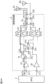
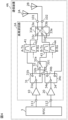
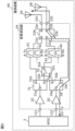
- FIG. 1 is a circuit configuration diagram of a high frequency circuit and a communication device according to an embodiment.
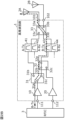
- FIG. 2A is a diagram showing a circuit state when a band A signal is transmitted alone in the high frequency circuit according to the embodiment.
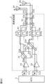
- FIG. 2B is a diagram showing a circuit state when a band B signal is transmitted alone in the high frequency circuit according to the embodiment.
- FIG. 2C is a diagram showing a circuit state when a band A signal and a band B signal are simultaneously transmitted in the high frequency circuit according to the embodiment.
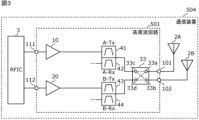
- FIG. 3 is a circuit configuration diagram of a high frequency circuit and a communication device according to a comparative example.
- FIG. 4 is a circuit configuration diagram of a high frequency circuit and a communication device according to a modification.
- FIG. 5 is a diagram showing a circuit state when transmitting a 2G signal in a high frequency circuit according to a modification.
- each figure is a schematic diagram with emphasis, omission, or ratio adjustment as appropriate to illustrate the present invention, and is not necessarily strictly illustrated, and the actual shape, positional relationship, and ratio may differ. It may be different.
- substantially the same configurations are denoted by the same reference numerals, and overlapping explanations may be omitted or simplified.
- connection means not only the case of direct connection with a connection terminal and/or wiring conductor, but also the case of electrical connection through other circuit elements.
- connected between A and B means connected to A and B on a route connecting A and B.
- a "transmission path” refers to a transmission line that includes wiring through which a high-frequency transmission signal propagates, electrodes directly connected to the wiring, and terminals directly connected to the wiring or the electrodes. It means something.
- “receiving path” means a transmission line consisting of wiring through which high-frequency received signals propagate, electrodes directly connected to the wiring, and terminals directly connected to the wiring or the electrodes. do.
- each of the first band (band A) and the second band (band B) is defined by a standardization organization or the like for a communication system constructed using radio access technology (RAT). It means a frequency band predefined by (for example, 3GPP (registered trademark) (3rd Generation Partnership Project), IEEE (Institute of Electrical and Electronics Engineers), etc.).
- the communication systems include, for example, a 2G (2nd Generation) system, a 4G (4th Generation)-LTE (Long Term Evolution) system, a 5G (5th Generation)-NR (New Radio) system, and A WLAN (Wireless Local Area Network) system or the like can be used, but is not limited thereto.
- FIG. 1 is a circuit configuration diagram of a high frequency circuit 1 and a communication device 4 according to an embodiment.
- a communication device 4 includes a high frequency circuit 1, antennas 2A and 2B, and an RF signal processing circuit (RFIC) 3.
- RFIC RF signal processing circuit
- the high frequency circuit 1 transmits high frequency signals between the antennas 2A and 2B and the RFIC 3.
- the detailed circuit configuration of the high frequency circuit 1 will be described later.
- the antenna 2A is connected to the antenna connection terminal 101 of the high frequency circuit 1, transmits the high frequency signal output from the high frequency circuit 1, and also receives a high frequency signal from the outside and outputs it to the high frequency circuit 1.
- the antenna 2B is connected to the antenna connection terminal 102 of the high frequency circuit 1, transmits the high frequency signal output from the high frequency circuit 1, and also receives a high frequency signal from the outside and outputs it to the high frequency circuit 1.
- the RFIC 3 is an example of a signal processing circuit that processes high frequency signals. Specifically, the RFIC 3 processes a transmission signal input from a baseband signal processing circuit (BBIC: not shown) by up-converting or the like, and transmits the high-frequency transmission signal generated by the signal processing to the high-frequency circuit. Output to transmission route 1. Further, the RFIC 3 processes the high frequency received signal input via the reception path of the high frequency circuit 1 by down-converting or the like, and outputs the received signal generated by the signal processing. Furthermore, the RFIC 3 has a control section that controls the switches, amplifiers, etc. that the high frequency circuit 1 has. Note that part or all of the function of the control unit of the RFIC 3 may be implemented outside the RFIC 3, for example, in the BBIC or the high frequency circuit 1.
- BBIC baseband signal processing circuit
- the antennas 2A and 2B are not essential components.
- the high frequency circuit 1 includes power amplifiers 10 and 20, filters 41, 42, 43 and 44, switches 31, 32 and 33, antenna connection terminals 101 and 102, high frequency input terminals 111 and 112.
- the antenna connection terminal 101 is an external connection terminal that the high frequency circuit 1 has, and is connected to the antenna 2A.
- the antenna connection terminal 102 is an external connection terminal included in the high frequency circuit 1, and is connected to the antenna 2B.
- the high frequency input terminals 111 and 112 are external connection terminals that the high frequency circuit 1 has, and are terminals for receiving a high frequency transmission signal from the RFIC 3. Note that each of the antenna connection terminals 101 and 102, the high frequency input terminals 111 and 112, and the terminals of the switches 31 to 33 described later may be a metal conductor such as a metal electrode or a metal bump, or may be a metal conductor such as a metal electrode or a metal bump. It may be one point (node).
- the power amplifier 10 is an example of a first power amplifier, and has an input end connected to the high frequency input terminal 111 and an output end connected to the common terminal 31a of the switch 31. Power amplifier 10 can amplify band A signals and band B signals.
- the power amplifier 20 is an example of a second power amplifier, and has an input end connected to the high frequency input terminal 112 and an output end connected to the terminal 32c of the switch 32. Power amplifier 20 can amplify band B signals.
- Each of power amplifiers 10 and 20 has an amplification transistor.
- the amplification transistor is, for example, a bipolar transistor such as a heterojunction bipolar transistor (HBT), or a field effect transistor such as a metal-oxide-semiconductor field effect transistor (MOSFET).
- HBT heterojunction bipolar transistor
- MOSFET metal-oxide-semiconductor field effect transistor
- the power amplifier 10 may be able to output a first maximum transmission power
- the power amplifier 20 may be able to output a second maximum transmission power that is higher than the first maximum transmission power. More specifically, the power amplifier 10 is capable of outputting a transmission signal of a first power class, and the power amplifier 20 is capable of outputting a transmission signal of a second power class having a maximum output power greater than the maximum output power of the first power class. It is possible to output signals.
- the power amplifier 20 is capable of handling higher power than the power amplifier 10, a large current flows and a low impedance output matching circuit is required, resulting in a larger circuit scale and deterioration in power efficiency. there's a possibility that.
- the power amplifier 10 is used instead of the power amplifier 20 when transmitting band A and band B signals individually, it is possible to improve the power efficiency of the high frequency circuit 1. It becomes possible.
- the power class is a classification of the output power of a UE (User Equipment) defined by the maximum output power, etc., and the smaller the value of the power class, the higher the output power is allowed.
- the maximum output power allowed in power class 1 is 31 dBm
- the maximum output power allowed in power class 1.5 is 29 dBm
- the maximum output power allowed in power class 2 is 26 dBm
- the maximum output power allowed in power class 3 is 23 dBm.
- the maximum output power of the UE is defined as the output power at the antenna end of the UE.
- the maximum output power of the UE is measured, for example, by a method defined by 3GPP (registered trademark) or the like.
- the maximum output power is measured by measuring the radiated power at antenna 2A or 2B.
- the output power of the antenna 2A or 2B can be measured by providing a terminal near the antenna 2A or 2B and connecting a measuring device (for example, a spectrum analyzer) to the terminal. You can also do it.
- the filter 41 is an example of a first filter, and is a transmission filter that includes band A in its passband.
- the input end of the filter 41 is connected to the terminal 31b of the switch 31, and the output end is connected to the antenna connection terminal 101 or 102 via the switch 33.
- the filter 42 is a reception filter that includes band A in its passband.
- the input end of the filter 42 is connected to the antenna connection terminal 101 or 102 via the switch 33, and the output end is connected to a low noise amplifier (not shown).
- the filter 43 is an example of a second filter, and is a transmission filter whose pass band includes band B, which is different from band A.
- the input end of the filter 43 is connected to the common terminal 32a of the switch 32, and the output end is connected to the antenna connection terminal 101 or 102 via the switch 33.
- the filter 44 is a reception filter whose passband includes band B.
- the input end of the filter 44 is connected to the antenna connection terminal 101 or 102 via the switch 33, and the output end is connected to a low noise amplifier (not shown).
- Filters 41 and 42 constitute a duplexer that transmits and receives band A signals.
- Filters 43 and 44 constitute a duplexer that transmits and receives band B signals. Note that in the high frequency circuit 1 according to this embodiment, the filters 42 and 44 may not be provided.
- the switch 31 is an example of a first switch, is connected between the power amplifier 10 and the filters 41 and 43, and connects the power amplifier 10 and the filter 41, and connects the power amplifier 10 and the filter 43. Switch.
- the switch 32 is an example of a second switch, is connected between the switch 31 and the power amplifier 20, and the filter 43, and is connected between the power amplifier 10 and the filter 43 and between the power amplifier 20 and the filter 43. Switch.
- the switch 31 has a common terminal 31a (first common terminal), a terminal 31b (first terminal), and a terminal 31c (second terminal).
- the switch 32 has a common terminal 32a (second common terminal), a terminal 32b (third terminal), and a terminal 32c (fourth terminal).
- the common terminal 31a is connected to the output end of the power amplifier 10
- the terminal 31b is connected to the input end of the filter 41
- the terminal 31c is connected to the terminal 32b
- the terminal 32c is connected to the output end of the power amplifier 20
- the common terminal 32a is connected to the input end of the filter 43.
- the switch 33 is an example of a fourth switch, and is connected between the filters 41 to 44 and the antenna connection terminals 101 and 102, switches the connection between the filter 41 and the antenna connection terminals 101 and 102, and switches the connection between the filter 41 and the antenna connection terminals 101 and 102.
- the connections with connection terminals 101 and 102 are switched.
- a band A signal can be transmitted and received by selecting one of the antennas 2A and 2B
- a band B signal can be transmitted and received by selecting one of the antennas 2A and 2B, depending on the antenna sensitivity situation. can be sent and received.
- the switch 33 has terminals 33a, 33b, 33c, and 33d.
- the switch 33 switches the connection between the terminal 33a and the terminals 33c and 33d, and switches the connection between the terminal 33b and the terminals 33c and 33d.
- the terminal 33a is connected to the antenna connection terminal 101
- the terminal 33b is connected to the antenna connection terminal 102
- the terminal 33c is connected to the output end of the filter 41 and the input end of the filter 42
- the terminal 33d is connected to the output end of the filter 43 and the input end of the filter 42. 44 input end.
- the switch 33 may be omitted, and the output end of the filter 41 and the input end of the filter 42 are directly connected to the antenna connection terminal 101, and the output end of the filter 43 and the input end of the filter 42 are connected directly to the antenna connection terminal 101. may be directly connected to the antenna connection terminal 102.
- band A signals can be transmitted and received by antenna 2A
- band B signals can be transmitted and received by antenna 2B.
- each of band A and band B is, for example, band B8 for 4G-LTE and band n8 for 5G-NR (transmission band: 880-915MHz, reception band 925-960MHz).
- Band B20 for 4G-LTE, Band n20 for 5G-NR transmission band: 832-862MHz, reception band 791-821MHz
- Band B26 for 4G-LTE, Band n26 for 5G-NR transmission band: 814-849MHz, reception band 859-894MHz
- band B28 for 4G-LTE or band n28 for 5G-NR (transmission band: 703-748MHz, reception band 758-803MHz).
- FIG. 2A is a diagram showing a circuit state when a band A signal is transmitted alone in the high frequency circuit 1 according to the embodiment.
- FIG. 2A shows a signal flow when a signal of band A of band A and band B is transmitted alone (hereinafter referred to as mode A).
- the band A transmission signal is transmitted through a transmission path including the high frequency input terminal 111, the power amplifier 10, the switch 31, the filter 41, the switch 33, the antenna connection terminal 101, and the antenna 2A.
- the terminal 33b and the terminal 33c may be in a connected state and the transmission signal of band A may be output from the antenna 2B depending on the antenna sensitivity situation.
- FIG. 2B is a diagram showing a circuit state when a band B signal is transmitted alone in the high frequency circuit 1 according to the embodiment.
- FIG. 2B shows a signal flow when a signal of band B of band A and band B is transmitted alone (hereinafter referred to as mode B).
- the common terminal 31a and the terminal 31c are in the connected state
- the common terminal 31a and the terminal 31b are in the disconnected state
- the common terminal 32a and the terminal 32b are in the connected state.
- the terminal 33a and the terminal 33d are in a connected state.
- the transmission signal of band B is transmitted through the transmission path of the high frequency input terminal 111, the power amplifier 10, the switch 31, the switch 32, the filter 43, the switch 33, the antenna connection terminal 101, and the antenna 2A.
- the terminal 33b and the terminal 33d may be in a connected state and the transmission signal of band B may be output from the antenna 2B depending on the antenna sensitivity situation.
- FIG. 2C is a diagram showing a circuit state when a band A signal and a band B signal are simultaneously transmitted in the high frequency circuit 1 according to the embodiment.
- FIG. 2C shows a signal flow when a band A signal and a band B signal are transmitted simultaneously (hereinafter referred to as mode C).
- the band A transmission signal is transmitted through a transmission path including the high frequency input terminal 111, the power amplifier 10, the switch 31, the filter 41, the switch 33, the antenna connection terminal 101, and the antenna 2A.
- the transmission signal of band B is transmitted through a transmission path including the high frequency input terminal 112, the power amplifier 20, the switch 32, the filter 43, the switch 33, the antenna connection terminal 102, and the antenna 2B.
- the terminal 33b and the terminal 33c are connected, the transmission signal of band A is output from the antenna 2B, the terminal 33a and the terminal 33d are connected, and the band The transmission signal B may be output from the antenna 2A.
- the signal path of the power amplifier 10 and the filter 41 is used to connect the power amplifier 10 and the filter 41.
- Signals can be transmitted independently.
- the band B signal can be transmitted independently through the signal path of the power amplifier 10 and the filter 43.
- the power amplifier 10 and the filter 41 are connected, and the power amplifier 20 and the filter 43 are connected, thereby transmitting a band A signal through the signal path of the power amplifier 10 and the filter 41.
- a band B signal can be transmitted through the signal path of the power amplifier 20 and filter 43.
- FIG. 3 is a circuit configuration diagram of a high frequency circuit 501 and a communication device 504 according to a comparative example.
- a high frequency circuit 501 shown in the figure includes power amplifiers 10 and 20, filters 41, 42, 43, and 44, a switch 33, antenna connection terminals 101 and 102, and high frequency input terminals 111 and 112. .
- the high frequency circuit 501 according to the comparative example differs from the high frequency circuit 1 according to the embodiment in that switches 31 and 32 are not added.
- the explanation will be omitted for the same points as the high frequency circuit 1 according to the embodiment, and will mainly be explained about the different points.
- the input end of the filter 41 is connected to the output end of the power amplifier 10, and the output end of the filter 41 is connected to the antenna connection terminal 101 or 102 via the switch 33.
- the input end of the filter 43 is connected to the output end of the power amplifier 20, and the output end of the filter 43 is connected to the antenna connection terminal 101 or 102 via the switch 33.
- the high frequency circuit 501 when a signal of band A of band A and band B is transmitted alone (mode A), terminal 33a and terminal 33c are in a connected state. At this time, the band A transmission signal is transmitted through a transmission path including the high frequency input terminal 111, the power amplifier 10, the filter 41, the switch 33, the antenna connection terminal 101, and the antenna 2A. Note that in mode A, the terminal 33b and the terminal 33c may be in a connected state, and the transmission signal of band A may be output from the antenna 2B.
- the terminal 33b and the terminal 33d are in a connected state.
- the band B transmission signal is transmitted through a transmission path including the high frequency input terminal 112, the power amplifier 20, the filter 43, the switch 33, the antenna connection terminal 102, and the antenna 2B.
- the terminal 33a and the terminal 33d may be in a connected state, and the transmission signal of band B may be output from the antenna 2A.
- the high frequency circuit 501 when simultaneously transmitting band A signals and band B signals (mode C), terminals 33a and 33c are connected, and terminals 33b and 33d are connected. state. At this time, the transmission signal of band A is transmitted through the transmission path of high frequency input terminal 111, power amplifier 10, filter 41, switch 33, antenna connection terminal 101, and antenna 2A, and at the same time, the transmission signal of band B is transmitted. , high frequency input terminal 112, power amplifier 20, filter 43, switch 33, antenna connection terminal 102, and antenna 2B.
- the terminal 33b and the terminal 33c may be in a connected state, and the transmission signal of band A may be output from the antenna 2B, and the terminal 33a and the terminal 33d may be in a connected state, and the transmission signal of band B is output from the antenna. It may be output from 2A.
- a band A signal can be transmitted singly through the signal path of the power amplifier 10 and the filter 41, and a band B signal can be transmitted singly through the signal path of the power amplifier 20 and the filter 43.
- a band A signal can be transmitted through a signal path including power amplifier 10 and filter 41, and at the same time, a band B signal can be transmitted through a signal path including power amplifier 20 and filter 43.
- the high frequency circuit 1 since it is not desired to increase the number of large-sized power amplifiers, the case where the band A signal is transmitted alone and the case where the band B signal is transmitted alone are different. , also serves as a power amplifier. Further, although the power amplifier 20 has a higher maximum transmission power than the power amplifier 10, the power amplifier 10 is used because the maximum transmission power does not need to be large when transmitting band B signals alone. Thereby, the power efficiency of the high frequency circuit 1 can be optimized.
- the power amplifier 10 and filter 41 are connected by switching the switch 31, and the signal in band B out of band A and band B is transmitted.
- power amplifier 10 and filter 43 are connected by switching switches 31 and 32.
- the switches 31 and 32 when simultaneously transmitting a band A signal and a band B signal, by switching the switches 31 and 32, the power amplifier 10 and the filter 41 are connected, and the power amplifier 20 and the filter 43 are connected. .
- FIG. 4 is a circuit configuration diagram of a high frequency circuit 1A and a communication device 4A according to a modification.
- the communication device 4A includes a high frequency circuit 1A, antennas 2A and 2B, and an RFIC 3.
- the communication device 4A according to this modification differs from the communication device 4 according to the embodiment only in the circuit configuration of the high frequency circuit 1A.
- the circuit configuration of the high frequency circuit 1A according to this modification will be explained.
- the high frequency circuit 1A includes power amplifiers 10 and 20, filters 41, 42, 43 and 44, switches 31, 32, 33A and 34, antenna connection terminals 101 and 102, and high frequency input terminals 111 and 112. .
- the high frequency circuit 1A according to this modification is different from the high frequency circuit 1 according to the embodiment in that a switch 34 is added and the configuration of a switch 33A.
- the explanation of the same points as the high frequency circuit 1 according to the embodiment will be omitted, and the explanation will focus on the different points.
- the power amplifier 10 is an example of a first power amplifier, and has an input end connected to the high frequency input terminal 111 and an output end connected to the common terminal 31a. Power amplifier 10 can amplify band A signals and band B signals for 4G-LTE or 5G-NR.
- the power amplifier 20 is an example of a second power amplifier, and has an input end connected to the high frequency input terminal 112 and an output end connected to the common terminal 34a of the switch 34.
- the power amplifier 20 can amplify band B signals for 4G-LTE or 5G-NR as well as 2G signals.
- the power amplifier 10 can output a first maximum transmission power
- the power amplifier 20 can output a second maximum transmission power that is higher than the first maximum transmission power. More specifically, the power amplifier 10 is capable of outputting a transmission signal of a first power class, and the power amplifier 20 is capable of outputting a transmission signal of a second power class having a maximum output power larger than the maximum output power of the first power class. It is possible to output a transmission signal. Note that the maximum output power of the 2G signal is greater than the maximum output power of the 4G-LTE signal and the maximum output power of the 5G-NR signal.
- the power amplifier 20 is capable of handling higher power than the power amplifier 10, a large current flows and a low impedance output matching circuit is required, resulting in a larger circuit scale and deterioration in power efficiency. there's a possibility that.
- the filter 41 is an example of a first filter, and is a transmission filter that includes band A in its passband.
- the input end of the filter 41 is connected to the terminal 31b, and the output end is connected to the antenna connection terminal 101 or 102 via the switch 33A.
- the filter 43 is an example of a second filter, and is a transmission filter that includes band B in its passband.
- the input end of the filter 43 is connected to the common terminal 32a, and the output end is connected to the antenna connection terminal 101 or 102 via the switch 33A.
- the switch 31 is an example of a first switch, is connected between the power amplifier 10 and the filters 41 and 43, and connects the power amplifier 10 and the filter 41, and connects the power amplifier 10 and the filter 43. Switch.
- the switch 32 is an example of a second switch, is connected between the switches 31 and 34, and the filter 43, and switches the connection between the power amplifier 10 and the filter 43, and the connection between the power amplifier 20 and the filter 43. .
- the switch 34 is an example of a third switch, and is connected between the power amplifier 20, the switch 32, and the antenna connection terminals 101 and 102, and is connected between the power amplifier 20 and the filter 43, and between the power amplifier 20 and the switch. 32 and the connection to the antenna connection terminal 101 or 102 not via the filter 43 is switched.
- the switch 34 has a common terminal 34a (third common terminal), a terminal 34b (fifth terminal), and a terminal 34c (sixth terminal).
- the common terminal 34a is connected to the output end of the power amplifier 20, the terminal 34b is connected to the terminal 32c, and the terminal 34c is connected to the antenna connection terminal 101 or 102 via the switch 33A.
- the switch 33A is an example of a fourth switch, and is connected between the antenna connection terminals 101 and 102 and the filters 41 and 43 and the switch 34, and is connected between the antenna connection terminal 101 and any one of the filters 41 and 43 and the switch 34. The connection between the antenna connection terminal 102 and any one of the filters 41, 43 and the switch 34 is switched.
- the switch 33A has terminals 33a, 33b, 33c, 33d, and 33e.
- the terminal 33a is connected to the antenna connection terminal 101
- the terminal 33b is connected to the antenna connection terminal 102
- the terminal 33c is connected to the output end of the filter 41 and the input end of the filter 42
- the terminal 33d is connected to the output end of the filter 43 and the input end of the filter 42. 44
- the terminal 33e is directly connected to the terminal 34c.
- a band A signal can be transmitted and received by selecting one of the antennas 2A and 2B
- a band B signal can be transmitted and received by selecting one of the antennas 2A and 2B, depending on the antenna sensitivity situation.
- 2G signals can be transmitted by selecting either antenna 2A or 2B.
- the common terminal 31a and the terminal 31b are in a connected state
- the common terminal 31a and the terminal 31c are in a disconnected state
- the terminals 33a and 33c are in a connected state.
- the transmission signal of band A is transmitted through a transmission path including the high frequency input terminal 111, the power amplifier 10, the switch 31, the filter 41, the switch 33A, the antenna connection terminal 101, and the antenna 2A.
- the terminal 33b and the terminal 33c may be in a connected state and the transmission signal of band A may be output from the antenna 2B depending on the antenna sensitivity situation.
- the common terminal 31a and the terminal 31c are in a connected state
- the common terminal 31a and the terminal 31b are in a disconnected state
- the common terminal 32a and the terminal 32b are in a connected state
- the terminal 33a and the terminal 33d are in a connected state.
- the transmission signal of band B is transmitted through the transmission path of the high frequency input terminal 111, the power amplifier 10, the switch 31, the switch 32, the filter 43, the switch 33A, the antenna connection terminal 101, and the antenna 2A.
- the terminal 33b and the terminal 33d may be in a connected state and the transmission signal of band B may be output from the antenna 2B depending on the antenna sensitivity situation.
- the common terminal 31a and the terminal 31b are in a connected state
- the common terminal 31a and the terminal 31c are in a disconnected state
- the common terminal 34a and the terminal 34b are in a connected state
- the common terminal 34a and the terminal 34c are in a disconnected state
- the common terminal 32a and the terminal 32c are in a connected state
- the terminal 33a and the terminal 33c are in a connected state
- the terminal 33b and the terminal 33d are in a connected state.
- the transmission signal of band A is transmitted through a transmission path including the high frequency input terminal 111, the power amplifier 10, the switch 31, the filter 41, the switch 33A, the antenna connection terminal 101, and the antenna 2A.
- the transmission signal of band B is transmitted through a transmission path including the high frequency input terminal 112, the power amplifier 20, the switch 34, the switch 32, the filter 43, the switch 33A, the antenna connection terminal 102, and the antenna 2B.
- the terminal 33b and the terminal 33c are connected, the transmission signal of band A is output from the antenna 2B, the terminal 33a and the terminal 33d are connected, and the band The transmission signal B may be output from the antenna 2A.
- the power amplifier 10 and the filter 41 when transmitting a band A signal of bands A and B alone, the power amplifier 10 and the filter 41 are connected by switching the switch 31, and the power amplifier 10 and the filter 41 are connected.
- power amplifier 10 and filter 43 are connected by switching switches 31 and 32.
- the switches 31, 32, and 34 when simultaneously transmitting a band A signal and a band B signal, by switching the switches 31, 32, and 34, the power amplifier 10 and the filter 41 are connected, and the power amplifier 20 and the filter 43 are connected.
- Ru since the same power amplifier 10 is used when transmitting band A signals alone and when transmitting band B signals alone, the power when transmitting band A and band B signals alone is Efficiency can be similarly optimized.
- FIG. 5 is a diagram showing a circuit state when transmitting a 2G signal in a high frequency circuit 1A according to a modification.
- the common terminal 34a and the terminal 34c are in a connected state
- the common terminal 34a and the terminal 34b are in a disconnected state
- the terminal 33b and the terminal 33e are in a connected state. state.
- the 2G transmission signal is transmitted through a transmission path including the high frequency input terminal 112, the power amplifier 20, the switch 34, the switch 33A, the antenna connection terminal 102, and the antenna 2B.
- the terminal 33a and the terminal 33e may be in a connected state and a 2G transmission signal may be output from the antenna 2A depending on the antenna sensitivity situation.
- connection configuration of the high frequency circuit 1A shown in FIG. 2G signals can be transmitted through the signal path of connection terminal 101 or 102.
- the power amplifier 20 amplifies the 2G signal, which requires higher power transmission than the 4G and 5G signals, so there is no need for the power amplifier 10 to be compatible with high power. Therefore, the power efficiency of the power amplifier 10 used when transmitting a 4G or 5G band A signal alone and when transmitting a 4G or 5G band B signal alone can be optimized without reducing the power efficiency. Furthermore, since the high power transmission signal for 2G can be transmitted without going through the switch 32 and filter 43, the 2G signal can be transmitted with low loss.
- the high frequency circuit 1 includes the power amplifier 10 capable of outputting the first maximum transmission power and the power amplifier 20 capable of outputting the second maximum transmission power higher than the first maximum transmission power. , a filter 41 whose passband includes band A, a filter 43 whose passband includes band B different from band A, between the power amplifier 10 and the filter 41, and between the power amplifier 10 and the filter 43.
- a switch 31 is connected to the switch 31, and a switch 32 is connected between the switch 31 and the filter 43 and between the power amplifier 20 and the filter 43.
- the power amplifier 10 and the filter 41 when transmitting a band A signal alone, the power amplifier 10 and the filter 41 are connected by switching the switch 31, and when transmitting a band B signal alone, the power amplifier 10 and the filter 41 are connected by switching the switches 31 and 32. 10 and the filter 43 can be connected. Furthermore, when simultaneously transmitting a band A signal and a band B signal, the power amplifier 10 and the filter 41 can be connected, and the power amplifier 20 and the filter 43 can be connected by switching the switches 31 and 32. becomes possible. In other words, since the same power amplifier 10 can be used when transmitting band A signals alone and when transmitting band B signals alone, the power efficiency when transmitting band A and band B signals alone is can be similarly optimized. Therefore, power efficiency when amplifying high frequency signals in different frequency bands can be optimized.
- the power amplifier 20 can handle higher power than the power amplifier 10, the circuit scale becomes larger and the power efficiency may deteriorate.
- the power amplifier 10 is used instead of the power amplifier 20, so it is possible to improve the power efficiency of the high frequency circuit 1. becomes.
- the switches 31 and 32 control the connection between the power amplifier 10 and the filter 41 and the connection between the power amplifier 10 and the filter 43 when the power amplifier 10 is configured to be operable.
- the power amplifiers 10 and 20 are configured to be switchable and can operate simultaneously, the power amplifier 10 and the filter 41 are connected, and the power amplifier 20 and the filter 43 are connected. Good too.
- the switch 31 has a common terminal 31a, terminals 31b and 31c
- the switch 32 has a common terminal 32a, terminals 32b and 32c
- the common terminal 31a is the output terminal of the power amplifier 10.
- the terminal 31b is connected to the input end of the filter 41
- the terminal 31c is connected to the terminal 32b
- the terminal 32c is connected to the output end of the power amplifier 20
- the common terminal 32a is connected to the input end of the filter 43. You can leave it there.
- the switches 31 and 32 are used to connect the common terminal 31a and the terminal 31b, and to connect the common terminal 31a and the terminal 31c when the power amplifier 10 is configured to be operable.
- the connection between the terminal 32a and the terminal 32b is configured to be switchable and the power amplifiers 10 and 20 are configured to be able to operate simultaneously, the common terminal 31a and the terminal 31b are connected, and the common terminal 32a and the terminal 32c.
- switching between single transmission of a band A signal, single transmission of a band B signal, and simultaneous transmission of a band A signal and a band B signal can be realized by a switch configuration. Can be simplified.
- the power amplifier 10 may be able to amplify a band A signal and a band B signal
- the power amplifier 20 may be able to amplify a band B signal.
- the high frequency circuit 1A includes power amplifiers 10 and 20, a filter 41 whose passband includes band A, a filter 43 whose passband includes band B, and power amplifier 10 and filters 41 and 43.
- a switch 31 is connected between the power amplifier 10 and the filter 41, and a switch 31 is connected between the switch 31, the power amplifier 20, and the filter 43, and switches between the power amplifier 10 and the filter 41, and the power amplifier 20 and the filter 43.
- the antenna connection terminal 102 is connected between the power amplifier 20 and the switch 32, and the antenna connection terminals 101 and 102. It may also include a switch 34 for switching the connection.
- the high frequency circuit 1A may be configured to be able to connect the power amplifier 20 and the antenna connection terminal 101 or 102 without using the switch 32 and the filter 43.
- the power amplifier 20 when the power amplifier 20 amplifies a 2G signal that requires higher power transmission than 4G and 5G signals, the power amplifier 10 does not need to be compatible with high power. Therefore, the power efficiency of the power amplifier 10 used when transmitting a 4G or 5G band A signal alone and when transmitting a 4G or 5G band B signal alone can be optimized without reducing the power efficiency. Furthermore, since the high power transmission signal for 2G can be transmitted without going through the switch 32 and filter 43, the 2G signal can be transmitted with low loss.
- the power amplifier 10 can amplify the 4G-LTE signal and the 5G-NR signal
- the power amplifier 20 can amplify the 2G signal, the 4G-LTE signal, and the 5G signal.
- the switch 34 has a common terminal 34a, terminals 34b and 34c, the common terminal 34a is connected to the output end of the power amplifier 20, the terminal 34b is connected to the switch 32, and the terminal 34c is connected to the output terminal of the power amplifier 20. It may be connected to the antenna connection terminal 101 or 102.
- the switch 34 may be configured to enable connection between the common terminal 34a and the terminal 34c.
- switching between transmitting a 2G signal and transmitting a 4G or 5G signal can be realized by the switch configuration, so the high frequency circuit 1A can be simplified.
- the high frequency circuit 1A is further connected between the antenna connection terminals 101 and 102 and the filters 41, 43 and the switch 34, and the antenna connection terminal 101 is connected to any one of the filters 41, 43 and the switch 34.
- a switch 33A may be provided to switch the connection between the antenna connection terminal 102 and any one of the filters 41, 43 and the switch 34.
- a band A signal can be transmitted and received by selecting one of antennas 2A and 2B, and a band B signal can be transmitted and received by selecting one of antennas 2A and 2B, depending on the antenna sensitivity situation.
- 2G signals can be transmitted by selecting either antenna 2A or 2B.
- band A and band B are respectively band B8 for 4G-LTE, band n8 for 5G-NR, band B20 for 4G-LTE, and band B20 for 5G-NR.
- the communication device 4 includes an RFIC 3 that processes a high frequency signal, and a high frequency circuit 1 that transmits the high frequency signal between the RFIC 3 and the antennas 2A and 2B.
- the communication device 4 can achieve the same effects as the above effects of the high frequency circuit 1.
- the high frequency circuit and communication device according to the present invention have been described above based on the embodiments and modified examples, but the high frequency circuit and communication device according to the present invention are not limited to the above embodiments and modified examples. do not have.
- the present invention also includes modifications obtained by applying the above and various devices incorporating the above-mentioned high frequency circuit and communication device.
- circuit elements, wiring, etc. may be inserted between the paths connecting the respective circuit elements and signal paths shown in the drawings. It's okay.
- bands for 5G-NR or 4G-LTE were used, but in addition to or instead of 5G-NR or 4G-LTE, bands for other radio access technologies may be used.
- a communication band may be used.
- communication bands for wireless local area networks may be used.
- a millimeter wave band of 7 gigahertz or more may be used.
- the high frequency circuit 1, the antennas 2A and 2B, and the RFIC 3 constitute a millimeter wave antenna circuit, and a distributed constant filter, for example, may be used as the filter.
- ⁇ 1> a first power amplifier and a second power amplifier; a first filter whose passband includes the first band; a second filter that includes the second band in its passband; a first switch connected between the first power amplifier and the first filter and the second filter; A high frequency circuit comprising: the first switch and a second switch connected between the second power amplifier and the second filter.
- the first switch and the second switch are (1) Connection between the first power amplifier and the first filter, (2) Connection between the first power amplifier and the second filter, and (3) Connection between the first power amplifier and the first filter.
- the high frequency circuit according to ⁇ 1> which is configured to be able to switch connection and connection between the second power amplifier and the second filter.
- the first switch has a first common terminal, a first terminal, and a second terminal
- the second switch has a second common terminal, a third terminal, and a fourth terminal
- the first common terminal is connected to the output terminal of the first power amplifier
- the first terminal is connected to the input terminal of the first filter
- the second terminal is connected to the third terminal
- the fourth terminal is connected to the input terminal of the first filter.
- the high frequency circuit according to ⁇ 1> or ⁇ 2>, wherein the terminal is connected to the output end of the second power amplifier, and the second common terminal is connected to the input end of the second filter.
- the first switch and the second switch are (1) connection between the first common terminal and the first terminal, (2) connection between the first common terminal and the second terminal, and connection between the second common terminal and the third terminal, and ( 3)
- the high frequency circuit according to ⁇ 3> which is configured to be able to switch the connection between the first common terminal and the first terminal and the connection between the second common terminal and the fourth terminal.
- the first power amplifier is capable of amplifying the first band signal and the second band signal
- the high frequency circuit according to any one of ⁇ 1> to ⁇ 4>, wherein the second power amplifier is capable of amplifying the second band signal.
- the first power amplifier is capable of outputting a first maximum transmission power
- the high frequency circuit according to any one of ⁇ 1> to ⁇ 5>, wherein the second power amplifier is capable of outputting a second maximum transmission power higher than the first maximum transmission power.
- ⁇ 7> moreover, a first antenna connection terminal connected to one of the first filter and the second filter; a second antenna connection terminal connected to the other of the first filter and the second filter; connected between the second power amplifier, the second switch, the first antenna connection terminal, and the second antenna connection terminal, and connecting the second power amplifier and the second filter;
- the high frequency circuit according to any one of ⁇ 1> to ⁇ 6>, comprising a third switch that switches connection between the two power amplifiers and the first antenna connection terminal or the second antenna connection terminal.
- ⁇ 8> The high frequency according to ⁇ 7>, wherein the second power amplifier and the first antenna connection terminal or the second antenna connection terminal are configured to be connectable without going through the second switch and the second filter. circuit.
- the first power amplifier is capable of amplifying a 4G-LTE (Long Term Evolution) signal and a 5G (5th Generation)-NR (New Radio) signal,
- the third switch has a third common terminal, a fifth terminal, and a sixth terminal,
- the third common terminal is connected to the output terminal of the second power amplifier, the fifth terminal is connected to the second switch, and the sixth terminal is connected to the first antenna connection terminal or the second antenna connection terminal.
- the high frequency circuit according to any one of ⁇ 7> to ⁇ 9>, which is connected.
- the third switch is The high frequency circuit according to ⁇ 10>, which is configured to enable connection between the third common terminal and the sixth terminal.
- ⁇ 12> moreover, connected between the first antenna connection terminal and the second antenna connection terminal, and the first filter, the second filter, and the third switch; a fourth switch that switches a connection between the second antenna connection terminal and one of the first filter, the second filter, and the third switch;
- the high frequency circuit according to any one of ⁇ 7> to ⁇ 11>, comprising:
- Each of the first band and the second band includes band B8 for 4G-LTE, band n8 for 5G-NR, band B20 for 4G-LTE, band n20 for 5G-NR, and 4G.
- ⁇ 14> a signal processing circuit that processes high frequency signals
- a communication device comprising: the high frequency circuit according to any one of ⁇ 1> to ⁇ 13> that transmits the high frequency signal between the signal processing circuit and the antenna.
- the present invention can be widely used in communication devices such as mobile phones as a high frequency circuit placed in a front end section.
Landscapes
- Engineering & Computer Science (AREA)
- Computer Networks & Wireless Communication (AREA)
- Signal Processing (AREA)
- Power Engineering (AREA)
- Transmitters (AREA)
- Transceivers (AREA)
Abstract
Description
[1 高周波回路1および通信装置4の回路構成]
本実施の形態に係る高周波回路1および通信装置4の回路構成について、図1を参照しながら説明する。図1は、実施の形態に係る高周波回路1および通信装置4の回路構成図である。
まず、通信装置4の回路構成について説明する。図1に示すように、本実施の形態に係る通信装置4は、高周波回路1と、アンテナ2Aおよび2Bと、RF信号処理回路(RFIC)3と、を備える。
次に、高周波回路1の回路構成について説明する。図1に示すように、高周波回路1は、電力増幅器10および20と、フィルタ41、42、43および44と、スイッチ31、32および33と、アンテナ接続端子101および102と、高周波入力端子111および112と、を備える。
図2Aは、実施の形態に係る高周波回路1において、バンドAの信号を単独送信する場合の回路状態を示す図である。図2Aには、バンドAおよびバンドBのうちのバンドAの信号を単独送信する場合(以下、モードAと記す)の信号の流れが示されている。
図4は、変形例に係る高周波回路1Aおよび通信装置4Aの回路構成図である。同図に示すように、通信装置4Aは、高周波回路1Aと、アンテナ2Aおよび2Bと、RFIC3と、を備える。本変形例に係る通信装置4Aは、実施の形態に係る通信装置4と比較して、高周波回路1Aの回路構成のみが異なる。以下では、本変形例に係る高周波回路1Aの回路構成について説明する。
変形例に係る高周波回路1Aによれば、(1)バンドAの信号の単独送信(モードA)、(2)バンドBの信号の単独送信(モードB)、(3)バンドAの信号およびバンドBの信号の同時送信(モードC)、ならびに(4)2G用の信号の送信(モードD)を実行することが可能である。
以上のように、本実施の形態に係る高周波回路1は、第1最大送信電力を出力可能な電力増幅器10と、第1最大送信電力よりも高い第2最大送信電力を出力可能な電力増幅器20と、バンドAを通過帯域に含むフィルタ41と、バンドAと異なるバンドBを通過帯域に含むフィルタ43と、電力増幅器10とフィルタ41との間、かつ、電力増幅器10とフィルタ43との間に接続されたスイッチ31と、スイッチ31とフィルタ43との間、かつ、電力増幅器20とフィルタ43との間に接続されたスイッチ32と、を備える。
以上、本発明に係る高周波回路および通信装置について、実施の形態および変形例に基づいて説明したが、本発明に係る高周波回路および通信装置は、上記実施の形態および変形例に限定されるものではない。上記実施の形態および変形例における任意の構成要素を組み合わせて実現される別の実施の形態や、上記実施の形態および変形例に対して本発明の主旨を逸脱しない範囲で当業者が思いつく各種変形を施して得られる変形例や、上記高周波回路および通信装置を内蔵した各種機器も本発明に含まれる。
第1電力増幅器および第2電力増幅器と、
第1バンドを通過帯域に含む第1フィルタと、
第2バンドを通過帯域に含む第2フィルタと、
前記第1電力増幅器と前記第1フィルタおよび前記第2フィルタとの間に接続された第1スイッチと、
前記第1スイッチおよび前記第2電力増幅器と前記第2フィルタとの間に接続された第2スイッチと、を備える、高周波回路。
前記第1スイッチおよび前記第2スイッチは、
(1)前記第1電力増幅器と前記第1フィルタとの接続、(2)前記第1電力増幅器と前記第2フィルタとの接続、および(3)前記第1電力増幅器と前記第1フィルタとの接続かつ前記第2電力増幅器と前記第2フィルタとの接続、を切り替え可能に構成されている、<1>に記載の高周波回路。
前記第1スイッチは、第1共通端子、第1端子および第2端子を有し、
前記第2スイッチは、第2共通端子、第3端子および第4端子を有し、
前記第1共通端子が前記第1電力増幅器の出力端に接続され、前記第1端子が前記第1フィルタの入力端に接続され、前記第2端子が前記第3端子に接続され、前記第4端子が前記第2電力増幅器の出力端に接続され、前記第2共通端子が前記第2フィルタの入力端に接続されている、<1>または<2>に記載の高周波回路。
前記第1スイッチおよび前記第2スイッチは、
(1)前記第1共通端子と前記第1端子との接続、(2)前記第1共通端子と前記第2端子との接続かつ前記第2共通端子と前記第3端子との接続、および(3)前記第1共通端子と前記第1端子との接続かつ前記第2共通端子と前記第4端子との接続、を切り替え可能に構成されている、<3>に記載の高周波回路。
前記第1電力増幅器は、前記第1バンドの信号および前記第2バンドの信号を増幅可能であり、
前記第2電力増幅器は、前記第2バンドの信号を増幅可能である、<1>~<4>のいずれかに記載の高周波回路。
前記第1電力増幅器は、第1最大送信電力を出力可能であり、
前記第2電力増幅器は、前記第1最大送信電力よりも高い第2最大送信電力を出力可能である、<1>~<5>のいずれかに記載の高周波回路。
さらに、
前記第1フィルタおよび前記第2フィルタの一方に接続された第1アンテナ接続端子と、
前記第1フィルタおよび前記第2フィルタの他方に接続された第2アンテナ接続端子と、
前記第2電力増幅器と、前記第2スイッチ、前記第1アンテナ接続端子および前記第2アンテナ接続端子との間に接続され、前記第2電力増幅器と前記第2フィルタとの接続、および、前記第2電力増幅器と前記第1アンテナ接続端子または前記第2アンテナ接続端子との接続を切り替える第3スイッチと、を備える、<1>~<6>のいずれかに記載の高周波回路。
前記第2電力増幅器と前記第1アンテナ接続端子または前記第2アンテナ接続端子とを、前記第2スイッチおよび前記第2フィルタを介さずに接続可能に構成されている、<7>に記載の高周波回路。
前記第1電力増幅器は、4G-LTE(Long Term Evolution)の信号および5G(5th Generation)-NR(New Radio)の信号を増幅可能であり、
前記第2電力増幅器は、2G用の信号、4G-LTE用の信号および5G-NR用の信号を増幅可能である、<7>または<8>に記載の高周波回路。
前記第3スイッチは、第3共通端子、第5端子および第6端子を有し、
前記第3共通端子が前記第2電力増幅器の出力端に接続され、前記第5端子が前記第2スイッチに接続され、前記第6端子が前記第1アンテナ接続端子または前記第2アンテナ接続端子に接続されている、<7>~<9>のいずれかに記載の高周波回路。
前記第3スイッチは、
前記第3共通端子と前記第6端子との接続が可能となるように構成されている、<10>に記載の高周波回路。
さらに、
前記第1アンテナ接続端子および前記第2アンテナ接続端子と、前記第1フィルタ、前記第2フィルタおよび前記第3スイッチとの間に接続され、前記第1アンテナ接続端子と前記第1フィルタ、前記第2フィルタおよび前記第3スイッチのいずれか1つとの接続を切り替え、前記第2アンテナ接続端子と前記第1フィルタ、前記第2フィルタおよび前記第3スイッチのいずれか1つとの接続を切り替える第4スイッチを備える、<7>~<11>のいずれかに記載の高周波回路。
前記第1バンドおよび前記第2バンドのそれぞれは、4G-LTEのためのバンドB8、5G-NRのためのバンドn8、4G-LTEのためのバンドB20、5G-NRのためのバンドn20、4G-LTEのためのバンドB26、5G-NRのためのバンドn26、4G-LTEのためのバンドB28、または5G-NRのためのバンドn28、である、<1>~<12>のいずれかに記載の高周波回路。
高周波信号を処理する信号処理回路と、
前記信号処理回路とアンテナとの間で前記高周波信号を伝送する<1>~<13>のいずれかに記載の高周波回路と、備える、通信装置。
2A、2B アンテナ
3 RF信号処理回路(RFIC)
4、4A、504 通信装置
10、20 電力増幅器
31、32、33、33A、34 スイッチ
31a、32a、34a 共通端子
31b、31c、32b、32c、33a、33b、33c、33d、33e、34b、34c 端子
41、42、43、44 フィルタ
101、102 アンテナ接続端子
111、112 高周波入力端子
Claims (13)
- 第1最大送信電力を出力可能な第1電力増幅器と、
前記第1最大送信電力よりも高い第2最大送信電力を出力可能な第2電力増幅器と、
第1バンドを通過帯域に含む第1フィルタと、
前記第1バンドと異なる第2バンドを通過帯域に含む第2フィルタと、
前記第1電力増幅器と前記第1フィルタとの間、かつ、前記第1電力増幅器と前記第2フィルタとの間に接続された第1スイッチと、
前記第1スイッチと前記第2フィルタとの間、かつ、前記第2電力増幅器と前記第2フィルタとの間に接続された第2スイッチと、を備える、
高周波回路。 - 前記第1スイッチおよび前記第2スイッチは、
前記第1電力増幅器が動作可能に構成される場合において、
前記第1電力増幅器と前記第1フィルタとの接続、および、前記第1電力増幅器と前記第2フィルタとの接続、を切り替え可能に構成され、
前記第1電力増幅器および前記第2電力増幅器が同時動作可能に構成される場合において、
前記第1電力増幅器と前記第1フィルタとを接続し、かつ、前記第2電力増幅器と前記第2フィルタとを接続するよう構成されている、
請求項1に記載の高周波回路。 - 前記第1スイッチは、第1共通端子、第1端子および第2端子を有し、
前記第2スイッチは、第2共通端子、第3端子および第4端子を有し、
前記第1共通端子が前記第1電力増幅器の出力端に接続され、前記第1端子が前記第1フィルタの入力端に接続され、前記第2端子が前記第3端子に接続され、前記第4端子が前記第2電力増幅器の出力端に接続され、前記第2共通端子が前記第2フィルタの入力端に接続されている、
請求項1または2に記載の高周波回路。 - 前記第1スイッチおよび前記第2スイッチは、
前記第1電力増幅器が動作可能に構成される場合において、
前記第1共通端子と前記第1端子との接続、および、前記第1共通端子と前記第2端子との接続かつ前記第2共通端子と前記第3端子との接続、を切り替え可能に構成され、
前記第1電力増幅器および前記第2電力増幅器が同時動作可能に構成される場合において、前記第1共通端子と前記第1端子とを接続し、かつ、前記第2共通端子と前記第4端子とを接続するよう構成されている、
請求項3に記載の高周波回路。 - 前記第1電力増幅器は、前記第1バンドの信号および前記第2バンドの信号を増幅可能であり、
前記第2電力増幅器は、前記第2バンドの信号を増幅可能である、
請求項1~4のいずれか1項に記載の高周波回路。 - さらに、
前記第1フィルタおよび前記第2フィルタの一方に接続された第1アンテナ接続端子と、
前記第1フィルタおよび前記第2フィルタの他方に接続された第2アンテナ接続端子と、
前記第2電力増幅器と、前記第2スイッチ、前記第1アンテナ接続端子および前記第2アンテナ接続端子との間に接続され、前記第2電力増幅器と前記第2フィルタとの接続、および、前記第2電力増幅器と前記第1アンテナ接続端子または前記第2アンテナ接続端子との接続を切り替える第3スイッチと、を備える、
請求項1~5のいずれか1項に記載の高周波回路。 - 前記第2電力増幅器と前記第1アンテナ接続端子または前記第2アンテナ接続端子とを、前記第2スイッチおよび前記第2フィルタを介さずに接続可能に構成されている、
請求項6に記載の高周波回路。 - 前記第1電力増幅器は、4G-LTE(Long Term Evolution)用の信号および5G(5th Generation)-NR(New Radio)用の信号を増幅可能であり、
前記第2電力増幅器は、2G用の信号、4G-LTE用の信号および5G-NR用の信号を増幅可能である、
請求項6または7に記載の高周波回路。 - 前記第3スイッチは、第3共通端子、第5端子および第6端子を有し、
前記第3共通端子が前記第2電力増幅器の出力端に接続され、前記第5端子が前記第2スイッチに接続され、前記第6端子が前記第1アンテナ接続端子または前記第2アンテナ接続端子に接続されている、
請求項6~8のいずれか1項に記載の高周波回路。 - 前記第3スイッチは、
前記第3共通端子と前記第6端子との接続が可能となるように構成されている、
請求項9に記載の高周波回路。 - さらに、
前記第1アンテナ接続端子および前記第2アンテナ接続端子と、前記第1フィルタ、前記第2フィルタおよび前記第3スイッチとの間に接続され、前記第1アンテナ接続端子と前記第1フィルタ、前記第2フィルタおよび前記第3スイッチのいずれか1つとの接続を切り替え、前記第2アンテナ接続端子と前記第1フィルタ、前記第2フィルタおよび前記第3スイッチのいずれか1つとの接続を切り替える第4スイッチを備える、
請求項6~10のいずれか1項に記載の高周波回路。 - 前記第1バンドおよび前記第2バンドのそれぞれは、4G-LTEのためのバンドB8、5G-NRのためのバンドn8、4G-LTEのためのバンドB20、5G-NRのためのバンドn20、4G-LTEのためのバンドB26、5G-NRのためのバンドn26、4G-LTEのためのバンドB28、または5G-NRのためのバンドn28、である、
請求項1~11のいずれか1項に記載の高周波回路。 - 高周波信号を処理する信号処理回路と、
前記信号処理回路とアンテナとの間で前記高周波信号を伝送する請求項1~12のいずれか1項に記載の高周波回路と、備える、
通信装置。
Priority Applications (2)
| Application Number | Priority Date | Filing Date | Title |
|---|---|---|---|
| CN202380046309.1A CN119366114A (zh) | 2022-06-15 | 2023-03-23 | 高频电路和通信装置 |
| US18/976,378 US20250105863A1 (en) | 2022-06-15 | 2024-12-11 | Radio-frequency circuit and communication device |
Applications Claiming Priority (2)
| Application Number | Priority Date | Filing Date | Title |
|---|---|---|---|
| JP2022096554 | 2022-06-15 | ||
| JP2022-096554 | 2022-06-15 |
Related Child Applications (1)
| Application Number | Title | Priority Date | Filing Date |
|---|---|---|---|
| US18/976,378 Continuation US20250105863A1 (en) | 2022-06-15 | 2024-12-11 | Radio-frequency circuit and communication device |
Publications (1)
| Publication Number | Publication Date |
|---|---|
| WO2023243175A1 true WO2023243175A1 (ja) | 2023-12-21 |
Family
ID=89192684
Family Applications (1)
| Application Number | Title | Priority Date | Filing Date |
|---|---|---|---|
| PCT/JP2023/011547 Ceased WO2023243175A1 (ja) | 2022-06-15 | 2023-03-23 | 高周波回路および通信装置 |
Country Status (3)
| Country | Link |
|---|---|
| US (1) | US20250105863A1 (ja) |
| CN (1) | CN119366114A (ja) |
| WO (1) | WO2023243175A1 (ja) |
Citations (3)
| Publication number | Priority date | Publication date | Assignee | Title |
|---|---|---|---|---|
| WO2020054388A1 (ja) * | 2018-09-11 | 2020-03-19 | 株式会社村田製作所 | 高周波フロントエンドモジュールおよび通信装置 |
| JP2022013725A (ja) * | 2020-06-29 | 2022-01-18 | スカイワークス ソリューションズ,インコーポレイテッド | 二重接続電力増幅器システム |
| WO2022034818A1 (ja) * | 2020-08-13 | 2022-02-17 | 株式会社村田製作所 | 高周波モジュール |
-
2023
- 2023-03-23 WO PCT/JP2023/011547 patent/WO2023243175A1/ja not_active Ceased
- 2023-03-23 CN CN202380046309.1A patent/CN119366114A/zh active Pending
-
2024
- 2024-12-11 US US18/976,378 patent/US20250105863A1/en active Pending
Patent Citations (3)
| Publication number | Priority date | Publication date | Assignee | Title |
|---|---|---|---|---|
| WO2020054388A1 (ja) * | 2018-09-11 | 2020-03-19 | 株式会社村田製作所 | 高周波フロントエンドモジュールおよび通信装置 |
| JP2022013725A (ja) * | 2020-06-29 | 2022-01-18 | スカイワークス ソリューションズ,インコーポレイテッド | 二重接続電力増幅器システム |
| WO2022034818A1 (ja) * | 2020-08-13 | 2022-02-17 | 株式会社村田製作所 | 高周波モジュール |
Also Published As
| Publication number | Publication date |
|---|---|
| CN119366114A (zh) | 2025-01-24 |
| US20250105863A1 (en) | 2025-03-27 |
Similar Documents
| Publication | Publication Date | Title |
|---|---|---|
| US11316486B2 (en) | High frequency circuit and communication device | |
| US20210250054A1 (en) | Radio frequency circuit, radio frequency module, and communication device | |
| US12395197B2 (en) | Radio frequency circuit and communication device | |
| US11757415B2 (en) | High frequency amplifier circuit and communication device | |
| WO2022075253A1 (ja) | 高周波回路および通信装置 | |
| WO2022138001A1 (ja) | 高周波回路、高周波モジュールおよび通信装置 | |
| US12592726B2 (en) | Radio frequency module and communication device | |
| US12095489B2 (en) | High-frequency circuit and communication device | |
| WO2023243175A1 (ja) | 高周波回路および通信装置 | |
| WO2023120073A1 (ja) | 高周波回路および通信装置 | |
| WO2022264862A1 (ja) | 高周波回路および通信装置 | |
| WO2023112651A1 (ja) | 高周波モジュール及び信号増幅方法 | |
| WO2022209665A1 (ja) | 高周波回路および通信装置 | |
| US20260081637A1 (en) | Radio frequency circuit | |
| US20260066939A1 (en) | Radio frequency circuit | |
| US12519502B2 (en) | Radio-frequency circuit | |
| WO2024042910A1 (ja) | 高周波モジュールおよび通信装置 | |
| US20250202509A1 (en) | Radio frequency circuit | |
| WO2023189178A1 (ja) | 高周波モジュール | |
| US20230378918A1 (en) | Amplifier circuit and communication device | |
| WO2023189276A1 (ja) | 高周波回路および通信装置 | |
| WO2025215972A1 (ja) | 高周波回路及び通信装置 | |
| WO2025158788A1 (ja) | 高周波回路及び通信装置 | |
| WO2026034047A1 (ja) | 高周波回路及び通信装置 | |
| WO2026004369A1 (ja) | 高周波回路 |
Legal Events
| Date | Code | Title | Description |
|---|---|---|---|
| 121 | Ep: the epo has been informed by wipo that ep was designated in this application |
Ref document number: 23823479 Country of ref document: EP Kind code of ref document: A1 |
|
| WWE | Wipo information: entry into national phase |
Ref document number: 202380046309.1 Country of ref document: CN |
|
| NENP | Non-entry into the national phase |
Ref country code: DE |
|
| WWP | Wipo information: published in national office |
Ref document number: 202380046309.1 Country of ref document: CN |
|
| 122 | Ep: pct application non-entry in european phase |
Ref document number: 23823479 Country of ref document: EP Kind code of ref document: A1 |
|
| NENP | Non-entry into the national phase |
Ref country code: JP |