WO2023238498A1 - Analog circuit - Google Patents
Analog circuit Download PDFInfo
- Publication number
- WO2023238498A1 WO2023238498A1 PCT/JP2023/014588 JP2023014588W WO2023238498A1 WO 2023238498 A1 WO2023238498 A1 WO 2023238498A1 JP 2023014588 W JP2023014588 W JP 2023014588W WO 2023238498 A1 WO2023238498 A1 WO 2023238498A1
- Authority
- WO
- WIPO (PCT)
- Prior art keywords
- current
- power supply
- amplifier
- supply voltage
- output terminal
- Prior art date
Links
- 239000003990 capacitor Substances 0.000 claims description 20
- 230000000694 effects Effects 0.000 description 15
- 238000010586 diagram Methods 0.000 description 10
- 230000003044 adaptive effect Effects 0.000 description 4
- 239000010755 BS 2869 Class G Substances 0.000 description 2
- 238000006243 chemical reaction Methods 0.000 description 2
- 230000002542 deteriorative effect Effects 0.000 description 1
- 238000009499 grossing Methods 0.000 description 1
- 230000004048 modification Effects 0.000 description 1
- 238000012986 modification Methods 0.000 description 1
- 230000001151 other effect Effects 0.000 description 1
- 239000004065 semiconductor Substances 0.000 description 1
Images


Classifications
-
- H—ELECTRICITY
- H03—ELECTRONIC CIRCUITRY
- H03F—AMPLIFIERS
- H03F3/00—Amplifiers with only discharge tubes or only semiconductor devices as amplifying elements
- H03F3/181—Low frequency amplifiers, e.g. audio preamplifiers
-
- H—ELECTRICITY
- H03—ELECTRONIC CIRCUITRY
- H03M—CODING; DECODING; CODE CONVERSION IN GENERAL
- H03M1/00—Analogue/digital conversion; Digital/analogue conversion
- H03M1/66—Digital/analogue converters
- H03M1/74—Simultaneous conversion
Definitions
- the present technology relates to analog circuits. Specifically, the present technology relates to an analog circuit provided with an IDAC (Current Digital to Analog Converter).
- IDAC Current Digital to Analog Converter
- class G amplifiers that combine the advantages of class AB bias and adaptive power supplies are sometimes used to achieve both high sound quality and high efficiency.
- Adaptive power supplies sometimes use charge pump circuits that do not require inductance for voltage conversion.
- an audio system has been proposed in which a positive power supply voltage and a negative power supply voltage are respectively supplied to the upper power line and lower power line of the main amplifier ( For example, see Patent Document 1).
- This technology was created in view of this situation, and its purpose is to reduce the noise of analog circuits equipped with IDACs.
- This technology was developed to solve the above-mentioned problems, and its first aspect is to generate a differential current according to digital data based on a positive power supply voltage and a negative power supply voltage.
- the analog circuit includes a current generation section and a switching circuit that switches the output of the differential current based on the digital data. This brings about the effect that differential currents generated based on the positive power supply voltage and the negative power supply voltage are differentially output.
- the switching circuit further includes a first external output terminal and a second external output terminal that output the differential current to the outside, and the switching circuit is configured to output the differential current from the current generating section when the digital data is not input.
- the output may be separated from the first external output terminal and the second external output terminal. This brings about the effect that the first external output terminal and the second external output terminal are set to the ground potential when no digital data is input.
- the first external output terminal and the second external output terminal may be set to a ground potential when the digital data is not input. This brings about the effect that the voltage at the output terminal of the IDAC when no digital data is input becomes equal to the common mode voltage of the amplifier to which the differential current generated by the IDAC is input.
- the current generation unit includes a positive current generation unit that generates a positive current based on the positive power supply voltage, and a negative current generation unit that generates a negative current based on the negative power supply voltage.
- a first switching element that supplies the output of the positive current generation section to the first external output terminal; and a first switching element that supplies the output of the negative current generation section to the second external output terminal.
- a second switching element that supplies the output of the positive current generation section to the second external output terminal, and a third switching element that supplies the output of the negative current generation section to the first external output terminal.
- the first switching element and the second switching element are switched synchronously based on the digital data
- the third switching element and the fourth switching element are switched synchronously based on the digital data.
- the fifth switching element and the sixth switching element may be switched synchronously based on the digital data. This brings about the effect that, while outputting the differential current generated by the IDAC based on digital data, the differential current generated by the IDAC when no digital data is input is separated from the output of the IDAC.
- the positive current generation section includes a first cascode current mirror circuit
- the negative current generation section includes a second cascode current mirror circuit
- the first cascode current mirror circuit may include an operational amplifier used to generate a mirror source current
- the second cascode current mirror circuit may include a current source used to generate a mirror source current.
- the first aspect may further include a first capacitor that decouples the bias gate voltage of the first cascode current mirror circuit, and a second capacitor that decouples the bias gate voltage of the second cascode current mirror circuit. . This brings about the effect that the noise of the bias gate voltage is reduced.
- the device may further include a first charge pump circuit that generates the positive power supply voltage and the negative power supply voltage based on a single power supply voltage. This brings about the effect that a positive power supply voltage and a negative power supply voltage are supplied to the IDAC.
- the positive power supply voltage and the negative power supply voltage may be step-down voltages obtained by stepping down the single power supply voltage. This brings about the effect that the power consumption of the IDAC is reduced.
- the current generating section and the switching circuit may be provided for a plurality of systems, and the first charge pump circuit may be shared by the current generating section for the plurality of systems. This brings about the effect that DA conversion for a plurality of channels can be performed while suppressing an increase in circuit scale.
- the device may further include an amplifier that outputs a differential voltage based on the input of the differential current. This brings about the effect of improving the drive capability with differential current input.
- the amplifier may include a fully differential amplifier. This brings about the effect that distortion of the differential output is reduced.
- the amplifier includes an integrator that inputs the differential current generated by the current generation section, an inverting amplifier connected to a subsequent stage of the integrator, and an output of the inverting amplifier. It may also include a resistor that feeds back to the input of the integrator. This brings about the effect that noise can be reduced while increasing gain at low frequencies.
- the first aspect further includes a second charge pump circuit that adaptively generates a positive power supply voltage and a negative power supply voltage of the amplifier based on a single power supply voltage according to the output amplitude of the amplifier. Good too. This brings about the effect that a positive power supply voltage and a negative power supply voltage are supplied to the amplifier.
- the amplifiers may be provided for a plurality of systems, and the second charge pump circuit may be shared by the amplifiers for the plurality of systems. This brings about the effect that signals for a plurality of channels are amplified while suppressing an increase in circuit scale.
- FIG. 3 is a diagram showing a configuration example of an analog circuit according to the first embodiment.
- 1 is a diagram showing an example of a circuit configuration of an IDAC according to a first embodiment;
- FIG. 3 is a diagram showing an example of an output waveform of an IDAC and an output waveform of an amplifier according to the first embodiment.
- FIG. 7 is a diagram showing a configuration example of an analog circuit according to a second embodiment.
- FIG. 7 is a diagram showing a configuration example of an analog circuit according to a third embodiment.
- First embodiment (example of driving IDAC with half voltage of positive and negative power supply voltages) 2.
- Second embodiment (example of driving IDAC with positive and negative power supply voltages) 3.
- Third embodiment (example with two systems of IDAC and amplifier)
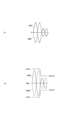
- FIG. 1 is a diagram showing a configuration example of an analog circuit according to the first embodiment.
- an analog circuit 100 is supplied with a positive power supply voltage and a negative power supply voltage. Then, analog circuit 100 generates differential voltages VOP and VON based on differential currents IOP and ION generated according to digital data DA, and drives speaker 105.
- Analog circuit 100 includes charge pump circuits 101 and 102, IDAC 103, and amplifier 104. Charge pump circuits 101 and 102, IDAC 103, and amplifier 104 may be integrated into one semiconductor chip, or may have a discrete configuration. The output of amplifier 104 is connected to speaker 105. Speaker 105 may be mounted on wireless headphones, for example.
- a power supply voltage AVD is supplied as a power supply to the charge pump circuit 101, and is connected to the ground potential GND.
- Charge pump circuit 101 generates a positive power supply voltage and a negative power supply voltage based on a single power supply voltage AVD, and supplies them to IDAC 103.
- the charge pump circuit 101 can generate a positive half voltage +AVD/2 and a negative half voltage -AVD/2 by stepping down the power supply voltage AVD, and supply them to the IDAC 103.
- a power supply voltage AVD is supplied as a power source to the charge pump circuit 102, and is connected to the ground potential GND.
- Charge pump circuit 102 adaptively generates a positive power supply voltage and a negative power supply voltage according to the output amplitude of amplifier 104 and supplies them to amplifier 104 .
- the charge pump circuit 102 generates a positive power supply voltage and a negative power supply voltage, and a positive step-down voltage and a negative step-down voltage obtained by stepping down the power supply voltage AVD, based on the single power supply voltage AVD, It may also be supplied to the amplifier 104.
- the charge pump circuit 102 generates a positive power supply voltage +AVD and a negative power supply voltage -AVD, and a positive half voltage +AVD/2 and a negative half voltage -AVD/2 based on a single power supply voltage AVD. can be generated and supplied to amplifier 104.
- IDAC 103 generates differential currents IOP and ION according to digital data DA based on positive half voltage +AVD/2 and negative half voltage -AVD/2 generated by charge pump circuit 101. At this time, the IDAC 103 can switch the output of the differential currents IOP and ION based on the digital data DA. For example, the IDAC 103 can separate the outputs of the differential currents IOP and ION from the amplifier 104 when no digital data DA is input. At this time, external output terminals TOP and TON of differential currents IOP and ION connected to amplifier 104 are set to ground potential GND. In order to reduce ripples in the output voltage from the charge pump circuit 101, the output voltage from the charge pump circuit 101 may be stabilized by a series regulator. Note that the IDAC 103 is an example of a current generation unit and a switching circuit described in the claims.
- Amplifier 104 generates differential voltages VOP and VON based on the input of differential currents IOP and ION generated by IDAC 103, and drives speaker 105.
- Amplifier 104 may constitute a multiple feedback filter. At this time, when the amplitudes of differential voltages VOP and VON are small, a positive half voltage +AVD/2 and a negative half voltage -AVD/2 are supplied from charge pump circuit 102 to amplifier 104. When the amplitudes of differential voltages VOP and VON are large, positive power supply voltage +AVD and negative power supply voltage -AVD are supplied from charge pump circuit 102 to amplifier 104.
- Amplifier 104 includes an integrator 106, an inverting amplifier 107, and resistors 151 and 152.
- Integrator 106 includes a fully differential amplifier 111 and capacitors 121 and 131.
- Inverting amplifier 107 includes a fully differential amplifier 112 and resistors 122, 132, 141, and 142.
- a non-inverting output terminal of the fully differential amplifier 111 is connected to an inverting input terminal of the fully differential amplifier 111 via a capacitor 121.
- the inverting output terminal of the fully differential amplifier 111 is connected to the non-inverting input terminal of the fully differential amplifier 111 via a capacitor 131.
- Differential currents IOP and ION are input from the IDAC 103 to an inverting input terminal and a non-inverting input terminal of the fully differential amplifier 111, respectively.
- a non-inverting output terminal of the fully differential amplifier 112 is connected to an inverting input terminal of the fully differential amplifier 112 via a resistor 122.
- the inverting output terminal of the fully differential amplifier 112 is connected to the non-inverting input terminal of the fully differential amplifier 112 via a resistor 132.
- the inverting input terminal of the fully differential amplifier 112 is connected to the inverting output terminal of the fully differential amplifier 111 via a resistor 141.
- a non-inverting input terminal of the fully differential amplifier 112 is connected to a non-inverting output terminal of the fully differential amplifier 111 via a resistor 142.
- the non-inverting output terminal of the fully differential amplifier 112 is connected to the inverting input terminal of the fully differential amplifier 111 via a resistor 151.
- the inverting output terminal of the fully differential amplifier 112 is connected to the non-inverting input terminal of the fully differential amplifier 111 via a resistor 152.
- a non-inverting output terminal and an inverting output terminal of the fully differential amplifier 112 are connected to the speaker 105.
- the integrator 106 operates at high speed to follow changes in the differential currents IOP and ION output from the IDAC 103, and can adapt to the input response from the IDAC 103.
- the integrator 106 has a large output load resistance, so it can operate at high speed with low power, and the inverting amplifier 107 can have a low bandwidth and low gain, and is suitable for large output. be able to.
- low frequency noise of the inverting amplifier 107 is corrected by feedback and is not output. Therefore, even when the two fully differential amplifiers 111 and 112 are provided in the amplifier 104, the noise is not doubled, but only by the amount of the fully differential amplifier 111 in the first stage.
- the external output terminals TOP and TON of the IDAC 103 are connected to the external output terminals TAP and TAN of the amplifier 104 via resistors 151 and 152, respectively.
- external output terminals TOP and TON can be set to ground potential GND. Therefore, the voltages at the external output terminals TOP and TON of the IDAC 103 become equal to the common-mode voltages at the external output terminals TAP and TAN of the amplifier 104, and there is no need to shift the common-mode voltage output from the amplifier 104.
- noise accompanying the shift of the common mode voltage output from the amplifier 104 can be eliminated, and noise can be reduced.
- FIG. 1 shows an example in which the amplifier 104 outputs the differential voltages VOP and VON, it may be a single-output amplifier.
- FIG. 2 is a diagram showing an example of the circuit configuration of the IDAC according to the first embodiment.
- the IDAC 103 includes a positive current generation section 401, a negative current generation section 402, and a switching circuit 403. At this time, the IDAC 103 can operate as a current addition type DA converter.
- the positive current generation unit 401 generates a positive current based on the positive half voltage +AVD/2.
- the positive current generation section 401 includes an operational amplifier 510, resistors 511, 514, 531, 551, and 571, and PMOS transistors 512, 513, 532, 533, 552, 553, 572, and 573.
- the negative current generation unit 402 generates a negative current based on the negative half voltage -AVD/2.
- the negative current generation section 402 includes a current source 500, resistors 520, 521, 524, 541, 561, and 581, and NMOS transistors 501, 502, 522, 523, 542, 543, 562, 563, 582, and 583. Be prepared.
- the switching circuit 403 switches the output of the differential currents IOP and ION based on the digital data DA.
- the switching circuit 403 includes switching elements 534 to 536, 544 to 546, 554 to 556, 564 to 566, 574 to 576, and 584 to 586.
- the switching elements 534 to 536, 544 to 546, 554 to 556, 564 to 566, 574 to 576, and 584 to 586 may be MOS transistors.
- the positive current generation section 401 can configure a cascode current mirror circuit.
- a cascode current mirror circuit in the positive current generation section 401 the output impedance can be increased and the influence of ripples on the output voltage from the charge pump circuit 101 can be reduced.
- PMOS transistors 512 and 513 are connected in series with each other, and PMOS transistors 532 and 533 are connected in series with each other.
- PMOS transistors 552 and 553 are connected in series with each other, and PMOS transistors 572 and 573 are connected in series with each other.
- the series circuit of PMOS transistors 512 and 513 can act as a current copy source.
- the series circuit of PMOS transistors 532 and 533, the series circuit of PMOS transistors 552 and 553, and the series circuit of PMOS transistors 572 and 573 can each operate as current copy destinations.
- the number of series circuits of PMOS transistors to which the current is copied can be provided as many as the number of bits of the digital data DA.
- each PMOS transistor 512, 532, 552, and 572 are connected to the power supply terminal TVP via resistors 511, 531, 551, and 571, respectively.
- a positive half voltage +AVD/2 is supplied to the power supply terminal TVP.
- the gate of each PMOS transistor 532, 552 and 572 is connected to bias terminal TBP.
- the gate of PMOS transistor 532 is connected to the gate of PMOS transistor 512 via resistor 514, and the gate of PMOS transistor 512 is connected to the output terminal of operational amplifier 510.
- the inverting input terminal of the operational amplifier 510 is connected to the ground potential GND, and the non-inverting input terminal of the operational amplifier 510 is connected to the drain of the PMOS transistor 513.
- the operational amplifier 510 to generate the mirror source current of the positive current generating section 401, it is possible to reduce the power supply voltage supplied to the positive current generating section 401. Therefore, it is possible to stably operate the positive current generation section 401 based on the positive half voltage +AVD/2 generated by the charge pump circuit 101.
- a capacitor 515 is connected between the gate of the PMOS transistor 532 and the power supply terminal TVP. Resistor 514 and capacitor 515 can act as a low pass filter to attenuate bias current noise.
- Bias gate voltage BA2 is applied to the gates of PMOS transistors 513, 533, 553, and 573. The bias gate voltage BA2 can be set to a value that allows the cascode current mirror circuit of the positive current generation section 401 to operate stably while allowing the PMOS transistors 513, 533, 553, and 573 to operate in saturation.
- the series circuit of the PMOS transistors 532 and 533 and the resistor 531 can generate a positive current corresponding to the value of the first bit of the digital data DA.
- the series circuit of PMOS transistors 552 and 553 and resistor 551 can generate a positive current corresponding to the value of the second bit of digital data DA.
- the series circuit of PMOS transistors 572 and 573 and resistor 571 can generate a positive current corresponding to the value of the third bit of digital data DA.
- the negative side current generation section 402 can configure a cascode current mirror circuit.
- a cascode current mirror circuit in the negative side current generation section 402 the output impedance can be increased and the influence of ripples on the output voltage from the charge pump circuit 101 can be reduced.
- NMOS transistors 501 and 502 are connected in series
- NMOS transistors 522 and 523 are connected in series
- NMOS transistors 542 and 543 are connected in series.
- NMOS transistors 562 and 563 are connected in series with each other
- NMOS transistors 582 and 583 are connected in series with each other.
- the series circuit of NMOS transistors 501 and 502 can act as a current copy source.
- the series circuit of NMOS transistors 542 and 543, the series circuit of NMOS transistors 562 and 563, and the series circuit of NMOS transistors 582 and 583 can each operate as current copy destinations.
- the number of series circuits of NMOS transistors to which the current is copied can be provided as many as the number of bits of the digital data DA.
- the drains of the NMOS transistors 502, 522, 542, 562, and 582 are connected to the power supply terminal TVN via resistors 520, 521, 541, 561, and 581, respectively.
- a negative half voltage -AVD/2 is supplied to the power supply terminal TVN.
- the gate of each NMOS transistor 542, 562 and 582 is connected to bias terminal TBN.
- the gate of NMOS transistor 542 is connected to the gate of NMOS transistor 522 via resistor 524, and the gate of NMOS transistor 522 is connected to the gate of NMOS transistor 502. Further, the gate of the NMOS transistor 502 is connected to the drain of the NMOS transistor 501, and the current source 500 is connected to the drain of the NMOS transistor 501.
- a capacitor 525 is connected between the gate of the NMOS transistor 542 and the power supply terminal TVN. Resistor 524 and capacitor 525 can act as a low pass filter to attenuate bias current noise.
- a bias gate voltage BA1 is applied to the gates of NMOS transistors 501, 523, 543, 563, and 583. Bias gate voltage BA1 can be set to a value that allows the cascode current mirror circuit of negative side current generation section 402 to operate stably while allowing NMOS transistors 501, 523, 543, 563, and 583 to operate in saturation.
- the series circuit of the NMOS transistors 542 and 543 and the resistor 541 can generate a negative current corresponding to the value of the first bit of the digital data DA.
- the series circuit of NMOS transistors 562 and 563 and resistor 561 can generate a negative current corresponding to the value of the second bit of digital data DA.
- the series circuit of NMOS transistors 582 and 583 and resistor 581 can generate a negative current corresponding to the value of the third bit of digital data DA.
- a capacitor 591 is connected between the power supply terminal TVP and the bias terminal TBP, and a capacitor 592 is connected between the power supply terminal TVN and the bias terminal TBN.
- Capacitor 591 can decouple the bias gate voltage applied to the gates of PMOS transistors 512, 532, 552, and 572.
- Capacitor 592 can decouple the bias gate voltage applied to the gates of NMOS transistors 502, 522, 542, 562, and 582.
- Each capacitor 591 and 592 may be attached externally. At this time, each capacitor 591 and 592 may have a large capacity.
- Switching elements 534 and 544 are connected in series with each other, switching elements 535 and 545 are connected in series with each other, and switching elements 536 and 546 are connected in series with each other.
- a series circuit of switching elements 534 and 544, a series circuit of switching elements 535 and 545, and a series circuit of switching elements 536 and 546 are connected between the drain of PMOS transistor 533 and the drain of NMOS transistor 543. .
- Switching elements 554 and 564 are connected in series with each other, switching elements 555 and 565 are connected in series with each other, and switching elements 556 and 566 are connected in series with each other.
- a series circuit of switching elements 554 and 564, a series circuit of switching elements 555 and 565, and a series circuit of switching elements 556 and 566 are connected between the drain of PMOS transistor 553 and the drain of NMOS transistor 563. .
- Switching elements 574 and 584 are connected in series with each other, switching elements 575 and 585 are connected in series with each other, and switching elements 576 and 586 are connected in series with each other.
- a series circuit of switching elements 574 and 584, a series circuit of switching elements 575 and 585, and a series circuit of switching elements 576 and 586 are connected between the drain of PMOS transistor 573 and the drain of NMOS transistor 583. .
- a connection point between switching elements 534 and 544, a connection point between switching elements 554 and 564, and a connection point between switching elements 574 and 584 are connected to an external output terminal TOP.
- a connection point between switching elements 536 and 546, a connection point between switching elements 556 and 566, and a connection point between switching elements 576 and 586 are connected to external output terminal TON.
- a connection point between switching elements 535 and 545, a connection point between switching elements 555 and 565, and a connection point between switching elements 575 and 585 are connected to ground potential GND.
- the current flowing through the drain of the PMOS transistor 533 and the current flowing through the drain of the NMOS transistor 543 are caused to flow through the external output terminal TOP or TON. be able to.
- the current flowing through the drain of PMOS transistor 533 and the current flowing through the drain of NMOS transistor 543 can flow through the ground point.
- the current flowing through the drain of the PMOS transistor 553 and the current flowing through the drain of the NMOS transistor 563 are caused to flow through the external output terminal TOP or TON. be able to.
- the current flowing through the drain of PMOS transistor 553 and the current flowing through the drain of NMOS transistor 563 can flow through the ground point.
- the current flowing through the drain of the PMOS transistor 573 and the current flowing through the drain of the NMOS transistor 583 are caused to flow through the external output terminal TOP or TON. be able to.
- the current flowing through the drain of PMOS transistor 573 and the current flowing through the drain of NMOS transistor 583 can flow through the ground point.
- the voltages at the external output terminals TOP and TON of the IDAC 103 can be made equal to the common mode voltages at the external output terminals TAP and TAN of the amplifier 104, making it unnecessary to shift the common mode voltage output from the amplifier 104. Therefore, the noise accompanying the shift of the common mode voltage output from the amplifier 104 can be eliminated, and the noise of the analog circuit 100 can be reduced.
- FIG. 3 is a diagram showing an example of the output waveform of the IDAC and the output waveform of the amplifier according to the first embodiment. Note that a in FIG. 3 indicates the output waveform of the differential currents IOP and ION, and b in FIG. 3 indicates the output waveform of the differential voltages VOP and VON.
- the IDAC 103 generates differential currents IOP and ION in a stepwise manner according to the digital data DA, and outputs them via external output terminals TOP and TON, respectively.
- amplifier 104 generates differential voltages VOP and VON based on differential currents IOP and ION, and outputs them via external output terminals TAP and TAN, respectively.
- the waveforms of the differential voltages VOP and VON become waveforms obtained by smoothing the step-like waveforms of the differential currents IOP and ION.
- a positive power supply voltage +AVD and a negative power supply voltage -AVD, and a positive half voltage +AVD/2 and a negative half voltage -AVD/2 are switched according to the amplitudes of the differential voltages VOP and VON.
- the amplifier 104 can operate as a class G amplifier that combines a class AB bias and an adaptive power supply.
- the IDAC 103 generates the differential currents IOP and ION according to the digital data DA based on the positive power supply voltage and the negative power supply voltage.
- the IDAC 103 and the amplifier 104 can be connected without interposing the DAC amplifier between the IDAC 103 and the amplifier 104, and it is possible to prevent signal quality from deteriorating due to noise of the DAC amplifier.
- an inverting amplifier 107 is connected after the integrator 106, and the output of the inverting amplifier 107 is fed back to the input of the integrator 106. This makes it possible to increase the gain of the amplifier 104 at low frequencies while reducing noise.
- the IDAC 103 is provided that generates the differential currents IOP and ION according to the digital data DA based on the positive half voltage +AVD/2 and the negative half voltage -AVD/2.
- an IDAC 203 is provided that generates differential currents IOP and ION according to digital data DA based on power supply voltage AVD and negative power supply voltage -AVD generated by a charge pump circuit.
- FIG. 4 is a diagram showing a configuration example of an analog circuit according to the second embodiment.
- an analog circuit 200 includes a charge pump circuit 201 and an IDAC 203 in place of the charge pump circuit 101 and IDAC 103 of the first embodiment described above.
- the rest of the configuration of the analog circuit 200 of the second embodiment is similar to the configuration of the analog circuit 100 of the first embodiment described above.
- Charge pump circuit 201 is supplied with power supply voltage AVD and connected to ground potential GND.
- Charge pump circuit 101 generates negative power supply voltage -AVD based on single power supply voltage AVD and supplies it to IDAC 103.
- IDAC 203 generates differential currents IOP and ION according to digital data DA based on power supply voltage AVD and negative power supply voltage -AVD generated by charge pump circuit 201. At this time, the IDAC 203 can switch the output of the differential currents IOP and ION based on the digital data DA. For example, the IDAC 203 can separate the outputs of the differential currents IOP and ION from the amplifier 104 when no digital data DA is input.
- the IDAC 203 generates a differential current IOP according to the digital data DA based on the power supply voltage AVD and the negative power supply voltage -AVD generated by the charge pump circuit 201. Generate ION. Thereby, the operating margin of the IDAC 203 can be improved.
- FIG. 5 is a diagram showing a configuration example of an analog circuit according to the third embodiment.
- an analog circuit 300 includes an IDAC 303 and an amplifier 304 instead of the IDAC 103 and amplifier 104 of the first embodiment described above.
- the rest of the configuration of the analog circuit 300 of the third embodiment is similar to the configuration of the analog circuit 100 of the first embodiment described above.
- the IDAC 303 has an IDAC 313 added to the IDAC 103 of the first embodiment described above.
- IDAC 313 can be configured similarly to IDAC 103.
- the digital data DA1 is input to the IDAC 103, and the digital data DA2 is input to the IDAC 313.
- Digital data DA1 and DA2 are stereo data.
- the amplifier 304 has an amplifier 314 added to the amplifier 104 of the first embodiment described above.
- Amplifier 314 can be configured similarly to amplifier 104.
- An amplifier 314 is connected after the IDAC 313 .
- the output of amplifier 314 is connected to speaker 315.
- the charge pump circuit 101 is shared by the IDACs 103 and 313. At this time, charge pump circuit 101 can supply positive half voltage +AVD/2 and negative half voltage -AVD/2 to IDACs 103 and 313.
- Charge pump circuit 102 is shared by amplifiers 104 and 314. At this time, charge pump circuit 102 can supply positive power supply voltage +AVD, negative power supply voltage -AVD, and positive half voltage +AVD/2 and negative half voltage -AVD/2 to amplifiers 104 and 314. can.
- two systems of IDACs 103 and 313 and amplifiers 104 and 314 are provided in order to support stereo output.
- three or more IDACs and amplifiers may be provided.
- a single charge pump circuit may be shared by IDACs for three or more systems, or a separate charge pump circuit may be shared by amplifiers for three or more systems.
- the charge pump circuit 201 of the above-described second embodiment may be used instead of the charge pump circuit 101.
- analog circuits 100 to 300 described above may be applied to, for example, car audio or component audio in addition to wireless headphones, or may be applied to audio equipment attached to a monitor or television.
- the embodiments described above are examples for embodying the present technology, and the matters in the embodiments and the matters specifying the invention in the claims have a corresponding relationship, respectively.
- the matters specifying the invention in the claims and the matters in the embodiments of the present technology having the same names have a corresponding relationship.
- the present technology is not limited to the embodiments, and can be realized by making various modifications to the embodiments without departing from the gist thereof. Further, the effects described in this specification are merely examples and are not limited, and other effects may also be present.
- a current generation unit that generates a differential current according to digital data based on a positive power supply voltage and a negative power supply voltage; and a switching circuit that switches the output of the differential current based on the digital data.
- (2) further comprising a first external output terminal and a second external output terminal that output the differential current to the outside;
- the analog circuit according to (1) wherein the switching circuit separates the output from the current generation section from the first external output terminal and the second external output terminal when the digital data is not input.
- the first external output terminal and the second external output terminal are set to a ground potential when no digital data is input.
- the current generating section includes: a positive current generation section that generates a positive current based on the positive power supply voltage; and a negative current generation unit that generates a negative current based on the negative power supply voltage
- the switching circuit includes: a first switching element that supplies the output of the positive current generation section to the first external output terminal; a second switching element that supplies the output of the negative current generation section to the second external output terminal; a third switching element that supplies the output of the positive current generation section to the second external output terminal; a fourth switching element that supplies the output of the negative current generation section to the first external output terminal; a fifth switching element that sets the output of the positive current generation section to a ground potential; a sixth switching element that sets the output of the negative side current generation section to the ground potential,
- the first switching element and the second switching element are switched synchronously based on the digital data
- the third switching element and the fourth switching element are switched synchronously based on the digital data,
- the analog circuit according to any one of (1) to (3), wherein the fifth switching element and
- the positive current generation section includes a first cascode current mirror circuit
- the negative current generation section includes a second cascode current mirror circuit
- the first cascode current mirror circuit includes an operational amplifier used to generate a mirror source current
- (6) a first capacitor that decouples the bias gate voltage of the first cascode current mirror circuit;
- the current generation section and the switching circuit are provided for multiple systems, The analog circuit according to (7) or (8), wherein the first charge pump circuit is shared by the current generation units for the plurality of systems.
- the amplifier includes a fully differential amplifier.
- the amplifier is an integrator that receives the differential current generated by the current generation section; an inverting amplifier connected after the integrator; The analog circuit according to (10) or (11), further comprising a resistor that feeds back the output of the inverting amplifier to the input of the integrator. (13) From (10) above, further comprising a second charge pump circuit that adaptively generates a positive power supply voltage and a negative power supply voltage of the amplifier based on a single power supply voltage according to the output amplitude of the amplifier. 12) The analog circuit according to any one of 12). (14) The amplifier is provided for multiple systems, The analog circuit according to (13), wherein the second charge pump circuit is shared by the amplifiers of the plurality of systems.
Abstract
The purpose of the present invention is to reduce noise in an analog circuit equipped with an IDAC. This analog circuit includes a current generation unit and a switching circuit. The current generation unit generates a differential current corresponding to digital data on the basis of a positive power supply voltage and a negative power supply voltage. The switching circuit switches the differential current output on the basis of the digital data. A first external output terminal and a second external output terminal that output the differential current to the outside may be further provided. The switching circuit may separate the output from the current generation unit from the first external output terminal and the second external output terminal when no digital data are input.
Description
本技術は、アナログ回路に関する。詳しくは、本技術は、IDAC(Current Digital to Analog Converter)が設けられたアナログ回路に関する。
The present technology relates to analog circuits. Specifically, the present technology relates to an analog circuit provided with an IDAC (Current Digital to Analog Converter).
オーディオ機器では、高音質化と高効率化と両立させるために、AB級のバイアスと適応型電源の利点を組み合わせたG級アンプが用いられることがある。適応型電源としては、電圧変換にインダクタンスを必要としないチャージポンプ回路が用いられることがある。チャージポンプ回路を適応型電源として用いたアンプとして、例えば、正の電源電圧、負の電源電圧がそれぞれ、メインアンプの上側電源ライン、下側電源ラインに供給されるオーディオシステムが提案されている(例えば、特許文献1参照)。
In audio equipment, class G amplifiers that combine the advantages of class AB bias and adaptive power supplies are sometimes used to achieve both high sound quality and high efficiency. Adaptive power supplies sometimes use charge pump circuits that do not require inductance for voltage conversion. As an amplifier using a charge pump circuit as an adaptive power supply, for example, an audio system has been proposed in which a positive power supply voltage and a negative power supply voltage are respectively supplied to the upper power line and lower power line of the main amplifier ( For example, see Patent Document 1).
しかしながら、上述の従来技術では、正負電源で動作するメインアンプの入力を、単電源で動作するIDACを用いて生成すると、IDACとメインアンプとの直結が困難になる。このとき、単電源で動作するIDACの出力を正負電源で動作するメインアンプの入力として用いるために、IDACとメインアンプとの間にDAC用アンプを介在させると、DAC用アンプのノイズによる信号品質の低下を招くおそれがあった。
However, in the above-mentioned conventional technology, if the input of the main amplifier that operates on positive and negative power supplies is generated using an IDAC that operates on a single power supply, it becomes difficult to directly connect the IDAC and the main amplifier. At this time, in order to use the output of the IDAC that operates on a single power supply as the input of the main amplifier that operates on positive and negative power supplies, if a DAC amplifier is interposed between the IDAC and the main amplifier, the signal quality will be affected by the noise of the DAC amplifier. There was a risk that this would lead to a decrease in
本技術はこのような状況に鑑みて生み出されたものであり、IDACが設けられたアナログ回路の低ノイズ化を図ることを目的とする。
This technology was created in view of this situation, and its purpose is to reduce the noise of analog circuits equipped with IDACs.
本技術は、上述の問題点を解消するためになされたものであり、その第1の側面は、正の電源電圧および負の電源電圧に基づいて、デジタルデータに応じた差動電流を生成する電流生成部と、上記デジタルデータに基づいて上記差動電流の出力を切り替えるスイッチング回路とを具備するアナログ回路である。これにより、正の電源電圧および負の電源電圧に基づいて生成された差動電流が差動出力されるという作用をもたらす。
This technology was developed to solve the above-mentioned problems, and its first aspect is to generate a differential current according to digital data based on a positive power supply voltage and a negative power supply voltage. The analog circuit includes a current generation section and a switching circuit that switches the output of the differential current based on the digital data. This brings about the effect that differential currents generated based on the positive power supply voltage and the negative power supply voltage are differentially output.
また、第1の側面において、上記差動電流を外部に出力する第1外部出力端子および第2外部出力端子をさらに具備し、上記スイッチング回路は、上記デジタルデータの無入力時に上記電流生成部からの出力を上記第1外部出力端子および上記第2外部出力端子から分離してもよい。これにより、デジタルデータの無入力時に第1外部出力端子および第2外部出力端子が接地電位に設定されるという作用をもたらす。
Further, in the first aspect, the switching circuit further includes a first external output terminal and a second external output terminal that output the differential current to the outside, and the switching circuit is configured to output the differential current from the current generating section when the digital data is not input. The output may be separated from the first external output terminal and the second external output terminal. This brings about the effect that the first external output terminal and the second external output terminal are set to the ground potential when no digital data is input.
また、第1の側面において、上記デジタルデータの無入力時に上記第1外部出力端子および上記第2外部出力端子は、接地電位に設定されてもよい。これにより、デジタルデータの無入力時のIDACの出力端子の電圧が、IDACで生成された差動電流が入力されるアンプの同相電圧と等しくなるという作用をもたらす。
Furthermore, in the first aspect, the first external output terminal and the second external output terminal may be set to a ground potential when the digital data is not input. This brings about the effect that the voltage at the output terminal of the IDAC when no digital data is input becomes equal to the common mode voltage of the amplifier to which the differential current generated by the IDAC is input.
また、第1の側面において、上記電流生成部は、上記正の電源電圧に基づいて正電流を生成する正側電流生成部と、上記負の電源電圧に基づいて負電流を生成する負側電流生成部とを備え、上記スイッチング回路は、上記正側電流生成部の出力を上記第1外部出力端子に供給する第1スイッチング素子と、上記負側電流生成部の出力を上記第2外部出力端子に供給する第2スイッチング素子と、上記正側電流生成部の出力を上記第2外部出力端子に供給する第3スイッチング素子と、上記負側電流生成部の出力を上記第1外部出力端子に供給する第4スイッチング素子と、上記正側電流生成部の出力を接地電位に設定する第5スイッチング素子と、上記負側電流生成部の出力を上記接地電位に設定する第6スイッチング素子とを備え、上記第1スイッチング素子と上記第2スイッチング素子とは、上記デジタルデータに基づいて同期して切り替えられ、上記第3スイッチング素子と上記第4スイッチング素子とは、上記デジタルデータに基づいて同期して切り替えられ、上記第5スイッチング素子と上記第6スイッチング素子とは、上記デジタルデータに基づいて同期して切り替えられてもよい。これにより、デジタルデータに基づいてIDACで生成された差動電流を出力しつつ、デジタルデータの無入力時にIDACで生成された差動電流がIDACの出力から分離されるという作用をもたらす。
Further, in the first aspect, the current generation unit includes a positive current generation unit that generates a positive current based on the positive power supply voltage, and a negative current generation unit that generates a negative current based on the negative power supply voltage. a first switching element that supplies the output of the positive current generation section to the first external output terminal; and a first switching element that supplies the output of the negative current generation section to the second external output terminal. a second switching element that supplies the output of the positive current generation section to the second external output terminal, and a third switching element that supplies the output of the negative current generation section to the first external output terminal. a fourth switching element that sets the output of the positive current generation section to the ground potential, and a sixth switching element that sets the output of the negative current generation section to the ground potential, The first switching element and the second switching element are switched synchronously based on the digital data, and the third switching element and the fourth switching element are switched synchronously based on the digital data. The fifth switching element and the sixth switching element may be switched synchronously based on the digital data. This brings about the effect that, while outputting the differential current generated by the IDAC based on digital data, the differential current generated by the IDAC when no digital data is input is separated from the output of the IDAC.
また、第1の側面において、上記正側電流生成部は、第1カスコードカレントミラー回路を備え、上記負側電流生成部は、第2カスコードカレントミラー回路を備え、上記第1カスコードカレントミラー回路は、ミラー元の電流の生成に用いられるオペアンプを備え、上記第2カスコードカレントミラー回路は、ミラー元の電流の生成に用いられる電流源を備えてもよい。これにより、IDACに用いられる電源電圧のリップルの影響を低減しつつ、電源電圧の低電圧化が図れるという作用をもたらす。
Further, in the first aspect, the positive current generation section includes a first cascode current mirror circuit, the negative current generation section includes a second cascode current mirror circuit, and the first cascode current mirror circuit The second cascode current mirror circuit may include an operational amplifier used to generate a mirror source current, and the second cascode current mirror circuit may include a current source used to generate a mirror source current. This brings about the effect that the power supply voltage can be lowered while reducing the influence of ripples on the power supply voltage used in the IDAC.
また、第1の側面において、上記第1カスコードカレントミラー回路のバイアスゲート電圧をデカップする第1コンデンサと、上記第2カスコードカレントミラー回路のバイアスゲート電圧をデカップする第2コンデンサとを備えてもよい。これにより、バイアスゲート電圧のノイズが低減されるという作用をもたらす。
The first aspect may further include a first capacitor that decouples the bias gate voltage of the first cascode current mirror circuit, and a second capacitor that decouples the bias gate voltage of the second cascode current mirror circuit. . This brings about the effect that the noise of the bias gate voltage is reduced.
また、第1の側面において、単一電源電圧に基づいて、上記正の電源電圧および上記負の電源電圧を生成する第1チャージポンプ回路をさらに具備してもよい。これにより、正の電源電圧および負の電源電圧がIDACに供給されるという作用をもたらす。
Furthermore, in the first aspect, the device may further include a first charge pump circuit that generates the positive power supply voltage and the negative power supply voltage based on a single power supply voltage. This brings about the effect that a positive power supply voltage and a negative power supply voltage are supplied to the IDAC.
また、第1の側面において、上記正の電源電圧および上記負の電源電圧は、上記単一電源電圧が降圧された降圧電圧でもよい。これにより、IDACの消費電力が低減されるという作用をもたらす。
Furthermore, in the first aspect, the positive power supply voltage and the negative power supply voltage may be step-down voltages obtained by stepping down the single power supply voltage. This brings about the effect that the power consumption of the IDAC is reduced.
また、第1の側面において、上記電流生成部および上記スイッチング回路は複数系統分設けられ、上記第1チャージポンプ回路は、上記複数系統分の上記電流生成部で共用されてもよい。これにより、回路規模の増大を抑制しつつ、複数チャネル分のDA変換が可能となるという作用をもたらす。
Further, in the first aspect, the current generating section and the switching circuit may be provided for a plurality of systems, and the first charge pump circuit may be shared by the current generating section for the plurality of systems. This brings about the effect that DA conversion for a plurality of channels can be performed while suppressing an increase in circuit scale.
また、第1の側面において、上記差動電流の入力に基づいて差動電圧を出力するアンプをさらに具備してもよい。これにより、差動電流を入力としたドライブ能力が向上されるという作用をもたらす。
Furthermore, in the first aspect, the device may further include an amplifier that outputs a differential voltage based on the input of the differential current. This brings about the effect of improving the drive capability with differential current input.
また、第1の側面において、上記アンプは、完全差動アンプを含んでもよい。これにより、差動出力の歪が低減されるという作用をもたらす。
Furthermore, in the first aspect, the amplifier may include a fully differential amplifier. This brings about the effect that distortion of the differential output is reduced.
また、第1の側面において、上記アンプは、上記電流生成部で生成された差動電流を入力とする積分器と、上記積分器の後段に接続された反転増幅器と、上記反転増幅器の出力を上記積分器の入力に帰還する抵抗とを備えてもよい。これにより、低周波での利得を増大させつつ、低ノイズ化が図れるという作用をもたらす。
Further, in the first aspect, the amplifier includes an integrator that inputs the differential current generated by the current generation section, an inverting amplifier connected to a subsequent stage of the integrator, and an output of the inverting amplifier. It may also include a resistor that feeds back to the input of the integrator. This brings about the effect that noise can be reduced while increasing gain at low frequencies.
また、第1の側面において、単一電源電圧に基づいて、上記アンプの正の電源電圧および負の電源電圧を上記アンプの出力振幅に適応的に生成する第2チャージポンプ回路をさらに具備してもよい。これにより、正の電源電圧および負の電源電圧がアンプに供給されるという作用をもたらす。
The first aspect further includes a second charge pump circuit that adaptively generates a positive power supply voltage and a negative power supply voltage of the amplifier based on a single power supply voltage according to the output amplitude of the amplifier. Good too. This brings about the effect that a positive power supply voltage and a negative power supply voltage are supplied to the amplifier.
また、第1の側面において、上記アンプは複数系統分設けられ、上記第2チャージポンプ回路は、上記複数系統分の上記アンプで共用されてもよい。これにより、回路規模の増大を抑制しつつ、複数チャネル分の信号が増幅されるという作用をもたらす。
Furthermore, in the first aspect, the amplifiers may be provided for a plurality of systems, and the second charge pump circuit may be shared by the amplifiers for the plurality of systems. This brings about the effect that signals for a plurality of channels are amplified while suppressing an increase in circuit scale.
以下、本技術を実施するための形態(以下、実施の形態と称する)について説明する。説明は以下の順序により行う。
1.第1の実施の形態(正負の電源電圧の半電圧でIDACを駆動する例)
2.第2の実施の形態(正負の電源電圧でIDACを駆動する例)
3.第3の実施の形態(2系統のIDACおよびアンプを設けた例) Hereinafter, a mode for implementing the present technology (hereinafter referred to as an embodiment) will be described. The explanation will be given in the following order.
1. First embodiment (example of driving IDAC with half voltage of positive and negative power supply voltages)
2. Second embodiment (example of driving IDAC with positive and negative power supply voltages)
3. Third embodiment (example with two systems of IDAC and amplifier)
<1.第1の実施の形態>
図1は、第1の実施の形態に係るアナログ回路の構成例を示す図である。 <1. First embodiment>
FIG. 1 is a diagram showing a configuration example of an analog circuit according to the first embodiment.
図1は、第1の実施の形態に係るアナログ回路の構成例を示す図である。 <1. First embodiment>
FIG. 1 is a diagram showing a configuration example of an analog circuit according to the first embodiment.
同図において、アナログ回路100は、正の電源電圧および負の電源電圧が供給される。そして、アナログ回路100は、デジタルデータDAに応じた生成された差動電流IOPおよびIONに基づいて差動電圧VOPおよびVONを生成し、スピーカ105をドライブする。アナログ回路100は、チャージポンプ回路101および102と、IDAC103と、アンプ104とを備える。チャージポンプ回路101および102と、IDAC103と、アンプ104とは、1つの半導体チップに集積化してもよいし、ディスクリート構成であってもよい。アンプ104の出力は、スピーカ105に接続される。スピーカ105は、例えば、ワイヤレスヘッドフォンに搭載してもよい。
In the figure, an analog circuit 100 is supplied with a positive power supply voltage and a negative power supply voltage. Then, analog circuit 100 generates differential voltages VOP and VON based on differential currents IOP and ION generated according to digital data DA, and drives speaker 105. Analog circuit 100 includes charge pump circuits 101 and 102, IDAC 103, and amplifier 104. Charge pump circuits 101 and 102, IDAC 103, and amplifier 104 may be integrated into one semiconductor chip, or may have a discrete configuration. The output of amplifier 104 is connected to speaker 105. Speaker 105 may be mounted on wireless headphones, for example.
チャージポンプ回路101の電源として、電源電圧AVDが供給され、接地電位GNDに接続される。チャージポンプ回路101は、単一の電源電圧AVDに基づいて、正の電源電圧および負の電源電圧を生成し、IDAC103に供給する。例えば、チャージポンプ回路101は、電源電圧AVDを降圧した正の半電圧+AVD/2および負の半電圧-AVD/2を生成し、IDAC103に供給することができる。
A power supply voltage AVD is supplied as a power supply to the charge pump circuit 101, and is connected to the ground potential GND. Charge pump circuit 101 generates a positive power supply voltage and a negative power supply voltage based on a single power supply voltage AVD, and supplies them to IDAC 103. For example, the charge pump circuit 101 can generate a positive half voltage +AVD/2 and a negative half voltage -AVD/2 by stepping down the power supply voltage AVD, and supply them to the IDAC 103.
チャージポンプ回路102の電源として、電源電圧AVDが供給され、接地電位GNDに接続される。チャージポンプ回路102は、正の電源電圧および負の電源電圧をアンプ104の出力振幅に適応的に生成し、アンプ104に供給する。このとき、チャージポンプ回路102は、単一の電源電圧AVDに基づいて、正の電源電圧および負の電源電圧と、電源電圧AVDを降圧した正の降圧電圧および負の降圧電圧とを生成し、アンプ104に供給してもよい。例えば、チャージポンプ回路102は、単一の電源電圧AVDに基づいて、正の電源電圧+AVDおよび負の電源電圧-AVDと、正の半電圧+AVD/2および負の半電圧-AVD/2とを生成し、アンプ104に供給することができる。
A power supply voltage AVD is supplied as a power source to the charge pump circuit 102, and is connected to the ground potential GND. Charge pump circuit 102 adaptively generates a positive power supply voltage and a negative power supply voltage according to the output amplitude of amplifier 104 and supplies them to amplifier 104 . At this time, the charge pump circuit 102 generates a positive power supply voltage and a negative power supply voltage, and a positive step-down voltage and a negative step-down voltage obtained by stepping down the power supply voltage AVD, based on the single power supply voltage AVD, It may also be supplied to the amplifier 104. For example, the charge pump circuit 102 generates a positive power supply voltage +AVD and a negative power supply voltage -AVD, and a positive half voltage +AVD/2 and a negative half voltage -AVD/2 based on a single power supply voltage AVD. can be generated and supplied to amplifier 104.
IDAC103は、チャージポンプ回路101で生成された正の半電圧+AVD/2および負の半電圧-AVD/2に基づいて、デジタルデータDAに応じた差動電流IOPおよびIONを生成する。このとき、IDAC103は、デジタルデータDAに基づいて差動電流IOPおよびIONの出力を切り替えることができる。例えば、IDAC103は、デジタルデータDAの無入力時に差動電流IOPおよびIONの出力をアンプ104から分離することができる。このとき、アンプ104に接続される差動電流IOPおよびIONの外部出力端子TOPおよびTONは、接地電位GNDに設定される。チャージポンプ回路101からの出力電圧のリップルを低減するため、シリーズレギュレータによってチャージポンプ回路101からの出力電圧を安定化させてもよい。なお、IDAC103は、特許請求の範囲に記載の電流生成部およびスイッチング回路の一例である。
IDAC 103 generates differential currents IOP and ION according to digital data DA based on positive half voltage +AVD/2 and negative half voltage -AVD/2 generated by charge pump circuit 101. At this time, the IDAC 103 can switch the output of the differential currents IOP and ION based on the digital data DA. For example, the IDAC 103 can separate the outputs of the differential currents IOP and ION from the amplifier 104 when no digital data DA is input. At this time, external output terminals TOP and TON of differential currents IOP and ION connected to amplifier 104 are set to ground potential GND. In order to reduce ripples in the output voltage from the charge pump circuit 101, the output voltage from the charge pump circuit 101 may be stabilized by a series regulator. Note that the IDAC 103 is an example of a current generation unit and a switching circuit described in the claims.
アンプ104は、IDAC103で生成された差動電流IOPおよびIONの入力に基づいて、差動電圧VOPおよびVONを生成し、スピーカ105をドライブする。アンプ104は、多重帰還フィルタを構成してもよい。このとき、差動電圧VOPおよびVONの振幅が小さいときは、正の半電圧+AVD/2および負の半電圧-AVD/2がチャージポンプ回路102からアンプ104に供給される。差動電圧VOPおよびVONの振幅が大きいときは、正の電源電圧+AVDおよび負の電源電圧-AVDがチャージポンプ回路102からアンプ104に供給される。
Amplifier 104 generates differential voltages VOP and VON based on the input of differential currents IOP and ION generated by IDAC 103, and drives speaker 105. Amplifier 104 may constitute a multiple feedback filter. At this time, when the amplitudes of differential voltages VOP and VON are small, a positive half voltage +AVD/2 and a negative half voltage -AVD/2 are supplied from charge pump circuit 102 to amplifier 104. When the amplitudes of differential voltages VOP and VON are large, positive power supply voltage +AVD and negative power supply voltage -AVD are supplied from charge pump circuit 102 to amplifier 104.
アンプ104は、積分器106と、反転増幅器107と、抵抗151および152とを備える。積分器106は、完全差動アンプ111と、コンデンサ121および131とを備える。反転増幅器107は、完全差動アンプ112と、抵抗122、132,141および142とを備える。
Amplifier 104 includes an integrator 106, an inverting amplifier 107, and resistors 151 and 152. Integrator 106 includes a fully differential amplifier 111 and capacitors 121 and 131. Inverting amplifier 107 includes a fully differential amplifier 112 and resistors 122, 132, 141, and 142.
完全差動アンプ111の非反転出力端子は、コンデンサ121を介して完全差動アンプ111の反転入力端子に接続されている。完全差動アンプ111の反転出力端子は、コンデンサ131を介して完全差動アンプ111の非反転入力端子に接続されている。完全差動アンプ111の反転入力端子および非反転入力端子には、IDAC103から差動電流IOPおよびIONがそれぞれ入力される。
A non-inverting output terminal of the fully differential amplifier 111 is connected to an inverting input terminal of the fully differential amplifier 111 via a capacitor 121. The inverting output terminal of the fully differential amplifier 111 is connected to the non-inverting input terminal of the fully differential amplifier 111 via a capacitor 131. Differential currents IOP and ION are input from the IDAC 103 to an inverting input terminal and a non-inverting input terminal of the fully differential amplifier 111, respectively.
完全差動アンプ112の非反転出力端子は、抵抗122を介して完全差動アンプ112の反転入力端子に接続されている。完全差動アンプ112の反転出力端子は、抵抗132を介して完全差動アンプ112の非反転入力端子に接続されている。完全差動アンプ112の反転入力端子は、抵抗141を介して完全差動アンプ111の反転出力端子に接続されている。完全差動アンプ112の非反転入力端子は、抵抗142を介して完全差動アンプ111の非反転出力端子に接続されている。
A non-inverting output terminal of the fully differential amplifier 112 is connected to an inverting input terminal of the fully differential amplifier 112 via a resistor 122. The inverting output terminal of the fully differential amplifier 112 is connected to the non-inverting input terminal of the fully differential amplifier 112 via a resistor 132. The inverting input terminal of the fully differential amplifier 112 is connected to the inverting output terminal of the fully differential amplifier 111 via a resistor 141. A non-inverting input terminal of the fully differential amplifier 112 is connected to a non-inverting output terminal of the fully differential amplifier 111 via a resistor 142.
また、完全差動アンプ112の非反転出力端子は、抵抗151を介して完全差動アンプ111の反転入力端子に接続されている。完全差動アンプ112の反転出力端子は、抵抗152を介して完全差動アンプ111の非反転入力端子に接続されている。さらに、完全差動アンプ112の非反転出力端子および反転出力端子は、スピーカ105に接続されている。
Furthermore, the non-inverting output terminal of the fully differential amplifier 112 is connected to the inverting input terminal of the fully differential amplifier 111 via a resistor 151. The inverting output terminal of the fully differential amplifier 112 is connected to the non-inverting input terminal of the fully differential amplifier 111 via a resistor 152. Further, a non-inverting output terminal and an inverting output terminal of the fully differential amplifier 112 are connected to the speaker 105.
ここで、積分器106は、IDAC103から出力される差動電流IOPおよびIONの変化に追随するように高速動作し、IDAC103からの入力応答に適応することができる。このとき、積分器106は、出力負荷抵抗が大きくなるので、低電力で高速動作することができ、反転増幅器107は、低帯域化および低ゲイン化を図ることができ、大出力化に適応することができる。また、反転増幅器107の低周波ノイズは、フィードバックによって補正され、出力されない。このため、2つの完全差動アンプ111および112をアンプ104に設けた場合においても、ノイズは2倍ではなく、初段の完全差動アンプ111の分だけとなる。
Here, the integrator 106 operates at high speed to follow changes in the differential currents IOP and ION output from the IDAC 103, and can adapt to the input response from the IDAC 103. At this time, the integrator 106 has a large output load resistance, so it can operate at high speed with low power, and the inverting amplifier 107 can have a low bandwidth and low gain, and is suitable for large output. be able to. Further, low frequency noise of the inverting amplifier 107 is corrected by feedback and is not output. Therefore, even when the two fully differential amplifiers 111 and 112 are provided in the amplifier 104, the noise is not doubled, but only by the amount of the fully differential amplifier 111 in the first stage.
また、IDAC103の各外部出力端子TOPおよびTONは、各抵抗151および152を介してアンプ104の外部出力端子TAPおよびTANに接続される。このとき、デジタルデータDAの無入力時には、差動電流IOPおよびIONの出力をアンプ104から分離することにより、外部出力端子TOPおよびTONを接地電位GNDに設定することができる。このため、IDAC103の外部出力端子TOPおよびTONの電圧は、アンプ104の外部出力端子TAPおよびTANの同相電圧と等しくなり、アンプ104から出力される同相電圧のシフトが不要となる。この結果、アンプ104から出力される同相電圧のシフトに伴うノイズをなくすことができ、低ノイズ化を図ることができる。
Furthermore, the external output terminals TOP and TON of the IDAC 103 are connected to the external output terminals TAP and TAN of the amplifier 104 via resistors 151 and 152, respectively. At this time, when no digital data DA is input, by separating the outputs of differential currents IOP and ION from amplifier 104, external output terminals TOP and TON can be set to ground potential GND. Therefore, the voltages at the external output terminals TOP and TON of the IDAC 103 become equal to the common-mode voltages at the external output terminals TAP and TAN of the amplifier 104, and there is no need to shift the common-mode voltage output from the amplifier 104. As a result, noise accompanying the shift of the common mode voltage output from the amplifier 104 can be eliminated, and noise can be reduced.
なお、図1では、アンプ104として、差動電圧VOPおよびVONを出力する例を示したが、単一出力のアンプでもよい。
Although FIG. 1 shows an example in which the amplifier 104 outputs the differential voltages VOP and VON, it may be a single-output amplifier.
図2は、第1の実施の形態に係るIDACの回路構成の一例を示す図である。
FIG. 2 is a diagram showing an example of the circuit configuration of the IDAC according to the first embodiment.
同図において、IDAC103は、正側電流生成部401、負側電流生成部402およびスイッチング回路403を備える。このとき、IDAC103は、電流加算式DAコンバータとして動作することができる。
In the figure, the IDAC 103 includes a positive current generation section 401, a negative current generation section 402, and a switching circuit 403. At this time, the IDAC 103 can operate as a current addition type DA converter.
正側電流生成部401は、正の半電圧+AVD/2に基づいて正電流を生成する。正側電流生成部401は、オペアンプ510と、抵抗511、514、531、551および571と、PMOSトランジスタ512、513、532、533、552、553、572および573とを備える。
The positive current generation unit 401 generates a positive current based on the positive half voltage +AVD/2. The positive current generation section 401 includes an operational amplifier 510, resistors 511, 514, 531, 551, and 571, and PMOS transistors 512, 513, 532, 533, 552, 553, 572, and 573.
負側電流生成部402は、負の半電圧-AVD/2に基づいて負電流を生成する。負側電流生成部402は、電流源500と、抵抗520、521、524、541、561および581と、NMOSトランジスタ501、502、522、523、542、543、562、563、582および583とを備える。
The negative current generation unit 402 generates a negative current based on the negative half voltage -AVD/2. The negative current generation section 402 includes a current source 500, resistors 520, 521, 524, 541, 561, and 581, and NMOS transistors 501, 502, 522, 523, 542, 543, 562, 563, 582, and 583. Be prepared.
スイッチング回路403は、デジタルデータDAに基づいて差動電流IOPおよびIONの出力を切り替える。スイッチング回路403は、スイッチング素子534乃至536、544乃至546、554乃至556、564乃至566、574乃至576および584乃至586を備える。スイッチング素子534乃至536、544乃至546、554乃至556、564乃至566、574乃至576および584乃至586は、MOSトランジスタでもよい。
The switching circuit 403 switches the output of the differential currents IOP and ION based on the digital data DA. The switching circuit 403 includes switching elements 534 to 536, 544 to 546, 554 to 556, 564 to 566, 574 to 576, and 584 to 586. The switching elements 534 to 536, 544 to 546, 554 to 556, 564 to 566, 574 to 576, and 584 to 586 may be MOS transistors.
、
正側電流生成部401は、カスコードカレントミラー回路を構成することができる。正側電流生成部401にカスコードカレントミラー回路を用いることにより、出力インピーダンスを高め、チャージポンプ回路101からの出力電圧のリップルの影響を低減することができる。このとき、PMOSトランジスタ512および513は互いに直列接続され、PMOSトランジスタ532および533は互いに直列接続される。また、PMOSトランジスタ552および553は互いに直列接続され、PMOSトランジスタ572および573は互いに直列接続される。PMOSトランジスタ512および513の直列回路は、電流のコピー元として動作することができる。PMOSトランジスタ532および533の直列回路と、PMOSトランジスタ552および553の直列回路と、PMOSトランジスタ572および573の直列回路とはそれぞれ、電流のコピー先として動作することができる。電流のコピー先のPMOSトランジスタの直列回路は、デジタルデータDAのビット数分だけ設けることができる。 ,
The positivecurrent generation section 401 can configure a cascode current mirror circuit. By using a cascode current mirror circuit in the positive current generation section 401, the output impedance can be increased and the influence of ripples on the output voltage from the charge pump circuit 101 can be reduced. At this time, PMOS transistors 512 and 513 are connected in series with each other, and PMOS transistors 532 and 533 are connected in series with each other. Further, PMOS transistors 552 and 553 are connected in series with each other, and PMOS transistors 572 and 573 are connected in series with each other. The series circuit of PMOS transistors 512 and 513 can act as a current copy source. The series circuit of PMOS transistors 532 and 533, the series circuit of PMOS transistors 552 and 553, and the series circuit of PMOS transistors 572 and 573 can each operate as current copy destinations. The number of series circuits of PMOS transistors to which the current is copied can be provided as many as the number of bits of the digital data DA.
正側電流生成部401は、カスコードカレントミラー回路を構成することができる。正側電流生成部401にカスコードカレントミラー回路を用いることにより、出力インピーダンスを高め、チャージポンプ回路101からの出力電圧のリップルの影響を低減することができる。このとき、PMOSトランジスタ512および513は互いに直列接続され、PMOSトランジスタ532および533は互いに直列接続される。また、PMOSトランジスタ552および553は互いに直列接続され、PMOSトランジスタ572および573は互いに直列接続される。PMOSトランジスタ512および513の直列回路は、電流のコピー元として動作することができる。PMOSトランジスタ532および533の直列回路と、PMOSトランジスタ552および553の直列回路と、PMOSトランジスタ572および573の直列回路とはそれぞれ、電流のコピー先として動作することができる。電流のコピー先のPMOSトランジスタの直列回路は、デジタルデータDAのビット数分だけ設けることができる。 ,
The positive
各PMOSトランジスタ512、532、552および572のドレインは、抵抗511、531、551、571をそれぞれ介して電源端子TVPに接続されている。電源端子TVPには、正の半電圧+AVD/2が供給される。各PMOSトランジスタ532、552および572のゲートは、バイアス端子TBPに接続されている。PMOSトランジスタ532のゲートは、抵抗514を介してPMOSトランジスタ512のゲートに接続され、PMOSトランジスタ512のゲートは、オペアンプ510の出力端子に接続されている。オペアンプ510の反転入力端子は接地電位GNDに接続され、オペアンプ510の非反転入力端子は、PMOSトランジスタ513のドレインに接続されている。ここで、正側電流生成部401のミラー元の電流の生成にオペアンプ510を用いることにより、正側電流生成部401に供給される電源電圧の低電圧化を図ることができる。このため、チャージポンプ回路101で生成された正の半電圧+AVD/2に基づいて、正側電流生成部401を安定して動作させることが可能となる。
The drains of each PMOS transistor 512, 532, 552, and 572 are connected to the power supply terminal TVP via resistors 511, 531, 551, and 571, respectively. A positive half voltage +AVD/2 is supplied to the power supply terminal TVP. The gate of each PMOS transistor 532, 552 and 572 is connected to bias terminal TBP. The gate of PMOS transistor 532 is connected to the gate of PMOS transistor 512 via resistor 514, and the gate of PMOS transistor 512 is connected to the output terminal of operational amplifier 510. The inverting input terminal of the operational amplifier 510 is connected to the ground potential GND, and the non-inverting input terminal of the operational amplifier 510 is connected to the drain of the PMOS transistor 513. Here, by using the operational amplifier 510 to generate the mirror source current of the positive current generating section 401, it is possible to reduce the power supply voltage supplied to the positive current generating section 401. Therefore, it is possible to stably operate the positive current generation section 401 based on the positive half voltage +AVD/2 generated by the charge pump circuit 101.
PMOSトランジスタ532のゲートと電源端子TVPとの間には、コンデンサ515が接続されている。抵抗514およびコンデンサ515は、バイアス電流のノイズを減衰させるローパスフィルタとして動作することができる。PMOSトランジスタ513、533、553および573のゲートには、バイアスゲート電圧BA2が印加される。バイアスゲート電圧BA2は、PMOSトランジスタ513、533、553および573を飽和動作させつつ、正側電流生成部401のカスコードカレントミラー回路が安定して動作する値に設定することができる。
A capacitor 515 is connected between the gate of the PMOS transistor 532 and the power supply terminal TVP. Resistor 514 and capacitor 515 can act as a low pass filter to attenuate bias current noise. Bias gate voltage BA2 is applied to the gates of PMOS transistors 513, 533, 553, and 573. The bias gate voltage BA2 can be set to a value that allows the cascode current mirror circuit of the positive current generation section 401 to operate stably while allowing the PMOS transistors 513, 533, 553, and 573 to operate in saturation.
このとき、PMOSトランジスタ532および533と抵抗531との直列回路は、デジタルデータDAの1ビット目の値に対応した正の電流を生成することができる。PMOSトランジスタ552および553と抵抗551との直列回路は、デジタルデータDAの2ビット目の値に対応した正の電流を生成することができる。PMOSトランジスタ572および573と抵抗571との直列回路は、デジタルデータDAの3ビット目の値に対応した正の電流を生成することができる。
At this time, the series circuit of the PMOS transistors 532 and 533 and the resistor 531 can generate a positive current corresponding to the value of the first bit of the digital data DA. The series circuit of PMOS transistors 552 and 553 and resistor 551 can generate a positive current corresponding to the value of the second bit of digital data DA. The series circuit of PMOS transistors 572 and 573 and resistor 571 can generate a positive current corresponding to the value of the third bit of digital data DA.
負側電流生成部402は、カスコードカレントミラー回路を構成することができる。負側電流生成部402にカスコードカレントミラー回路を用いることにより、出力インピーダンスを高め、チャージポンプ回路101からの出力電圧のリップルの影響を低減することができる。このとき、NMOSトランジスタ501および502は互いに直列接続され、NMOSトランジスタ522および523は互いに直列接続され、NMOSトランジスタ542および543は互いに直列接続される。また、NMOSトランジスタ562および563は互いに直列接続され、NMOSトランジスタ582および583は互いに直列接続される。NMOSトランジスタ501および502の直列回路は、電流のコピー元として動作することができる。NMOSトランジスタ542および543の直列回路と、NMOSトランジスタ562および563の直列回路と、NMOSトランジスタ582および583の直列回路とはそれぞれ、電流のコピー先として動作することができる。電流のコピー先のNMOSトランジスタの直列回路は、デジタルデータDAのビット数分だけ設けることができる。
The negative side current generation section 402 can configure a cascode current mirror circuit. By using a cascode current mirror circuit in the negative side current generation section 402, the output impedance can be increased and the influence of ripples on the output voltage from the charge pump circuit 101 can be reduced. At this time, NMOS transistors 501 and 502 are connected in series, NMOS transistors 522 and 523 are connected in series, and NMOS transistors 542 and 543 are connected in series. Further, NMOS transistors 562 and 563 are connected in series with each other, and NMOS transistors 582 and 583 are connected in series with each other. The series circuit of NMOS transistors 501 and 502 can act as a current copy source. The series circuit of NMOS transistors 542 and 543, the series circuit of NMOS transistors 562 and 563, and the series circuit of NMOS transistors 582 and 583 can each operate as current copy destinations. The number of series circuits of NMOS transistors to which the current is copied can be provided as many as the number of bits of the digital data DA.
各NMOSトランジスタ502、522、542、562および582のドレインは、抵抗520、521、541、561、581をそれぞれ介して電源端子TVNに接続されている。電源端子TVNには、負の半電圧-AVD/2が供給される。各NMOSトランジスタ542、562および582のゲートは、バイアス端子TBNに接続されている。NMOSトランジスタ542のゲートは、抵抗524を介してNMOSトランジスタ522のゲートに接続され、NMOSトランジスタ522のゲートは、NMOSトランジスタ502のゲートに接続されている。また、NMOSトランジスタ502のゲートは、NMOSトランジスタ501のドレインに接続され、NMOSトランジスタ501のドレインには、電流源500が接続されている。
The drains of the NMOS transistors 502, 522, 542, 562, and 582 are connected to the power supply terminal TVN via resistors 520, 521, 541, 561, and 581, respectively. A negative half voltage -AVD/2 is supplied to the power supply terminal TVN. The gate of each NMOS transistor 542, 562 and 582 is connected to bias terminal TBN. The gate of NMOS transistor 542 is connected to the gate of NMOS transistor 522 via resistor 524, and the gate of NMOS transistor 522 is connected to the gate of NMOS transistor 502. Further, the gate of the NMOS transistor 502 is connected to the drain of the NMOS transistor 501, and the current source 500 is connected to the drain of the NMOS transistor 501.
NMOSトランジスタ542のゲートと電源端子TVNとの間には、コンデンサ525が接続されている。抵抗524およびコンデンサ525は、バイアス電流のノイズを減衰させるローパスフィルタとして動作することができる。NMOSトランジスタ501、523、543、563および583のゲートには、バイアスゲート電圧BA1が印加される。バイアスゲート電圧BA1は、NMOSトランジスタ501、523、543、563および583を飽和動作させつつ、負側電流生成部402のカスコードカレントミラー回路が安定して動作する値に設定することができる。
A capacitor 525 is connected between the gate of the NMOS transistor 542 and the power supply terminal TVN. Resistor 524 and capacitor 525 can act as a low pass filter to attenuate bias current noise. A bias gate voltage BA1 is applied to the gates of NMOS transistors 501, 523, 543, 563, and 583. Bias gate voltage BA1 can be set to a value that allows the cascode current mirror circuit of negative side current generation section 402 to operate stably while allowing NMOS transistors 501, 523, 543, 563, and 583 to operate in saturation.
このとき、NMOSトランジスタ542および543と抵抗541との直列回路は、デジタルデータDAの1ビット目の値に対応した負の電流を生成することができる。NMOSトランジスタ562および563と抵抗561との直列回路は、デジタルデータDAの2ビット目の値に対応した負の電流を生成することができる。NMOSトランジスタ582および583と抵抗581との直列回路は、デジタルデータDAの3ビット目の値に対応した負の電流を生成することができる。
At this time, the series circuit of the NMOS transistors 542 and 543 and the resistor 541 can generate a negative current corresponding to the value of the first bit of the digital data DA. The series circuit of NMOS transistors 562 and 563 and resistor 561 can generate a negative current corresponding to the value of the second bit of digital data DA. The series circuit of NMOS transistors 582 and 583 and resistor 581 can generate a negative current corresponding to the value of the third bit of digital data DA.
電源端子TVPとバイアス端子TBPとの間には、コンデンサ591が接続され、電源端子TVNとバイアス端子TBNとの間には、コンデンサ592が接続されている。コンデンサ591は、PMOSトランジスタ512、532、552および572のゲートに印加されるバイアスゲート電圧をデカップすることができる。コンデンサ592は、NMOSトランジスタ502、522、542、562および582のゲートに印加されるバイアスゲート電圧をデカップすることができる。各コンデンサ591および592は、外付けしてもよい。このとき、各コンデンサ591および592は、大容量化してもよい。
A capacitor 591 is connected between the power supply terminal TVP and the bias terminal TBP, and a capacitor 592 is connected between the power supply terminal TVN and the bias terminal TBN. Capacitor 591 can decouple the bias gate voltage applied to the gates of PMOS transistors 512, 532, 552, and 572. Capacitor 592 can decouple the bias gate voltage applied to the gates of NMOS transistors 502, 522, 542, 562, and 582. Each capacitor 591 and 592 may be attached externally. At this time, each capacitor 591 and 592 may have a large capacity.
スイッチング素子534および544は互いに直列に接続され、スイッチング素子535および545は互いに直列に接続され、スイッチング素子536および546は互いに直列に接続されている。スイッチング素子534および544の直列回路と、スイッチング素子535および545の直列回路と、スイッチング素子536および546の直列回路とは、PMOSトランジスタ533のドレインとNMOSトランジスタ543のドレインとの間に接続されている。
Switching elements 534 and 544 are connected in series with each other, switching elements 535 and 545 are connected in series with each other, and switching elements 536 and 546 are connected in series with each other. A series circuit of switching elements 534 and 544, a series circuit of switching elements 535 and 545, and a series circuit of switching elements 536 and 546 are connected between the drain of PMOS transistor 533 and the drain of NMOS transistor 543. .
スイッチング素子554および564は互いに直列に接続され、スイッチング素子555および565は互いに直列に接続され、スイッチング素子556および566は互いに直列に接続されている。スイッチング素子554および564の直列回路と、スイッチング素子555および565の直列回路と、スイッチング素子556および566の直列回路とは、PMOSトランジスタ553のドレインとNMOSトランジスタ563のドレインとの間に接続されている。
Switching elements 554 and 564 are connected in series with each other, switching elements 555 and 565 are connected in series with each other, and switching elements 556 and 566 are connected in series with each other. A series circuit of switching elements 554 and 564, a series circuit of switching elements 555 and 565, and a series circuit of switching elements 556 and 566 are connected between the drain of PMOS transistor 553 and the drain of NMOS transistor 563. .
スイッチング素子574および584は互いに直列に接続され、スイッチング素子575および585は互いに直列に接続され、スイッチング素子576および586は互いに直列に接続されている。スイッチング素子574および584の直列回路と、スイッチング素子575および585の直列回路と、スイッチング素子576および586の直列回路とは、PMOSトランジスタ573のドレインとNMOSトランジスタ583のドレインとの間に接続されている。
Switching elements 574 and 584 are connected in series with each other, switching elements 575 and 585 are connected in series with each other, and switching elements 576 and 586 are connected in series with each other. A series circuit of switching elements 574 and 584, a series circuit of switching elements 575 and 585, and a series circuit of switching elements 576 and 586 are connected between the drain of PMOS transistor 573 and the drain of NMOS transistor 583. .
スイッチング素子534および544の接続点と、スイッチング素子554および564の接続点と、スイッチング素子574および584の接続点とは、外部出力端子TOPに接続されている。スイッチング素子536および546の接続点と、スイッチング素子556および566の接続点と、スイッチング素子576および586の接続点とは、外部出力端子TONに接続されている。スイッチング素子535および545の接続点と、スイッチング素子555および565の接続点と、スイッチング素子575および585の接続点とは、接地電位GNDに接続される。
A connection point between switching elements 534 and 544, a connection point between switching elements 554 and 564, and a connection point between switching elements 574 and 584 are connected to an external output terminal TOP. A connection point between switching elements 536 and 546, a connection point between switching elements 556 and 566, and a connection point between switching elements 576 and 586 are connected to external output terminal TON. A connection point between switching elements 535 and 545, a connection point between switching elements 555 and 565, and a connection point between switching elements 575 and 585 are connected to ground potential GND.
デジタルデータDAの1ビット目の値が正のときは、スイッチング素子534および546がオンされ、PMOSトランジスタ533のドレインが外部出力端子TOPに接続され、NMOSトランジスタ543のドレインが外部出力端子TONに接続される。デジタルデータDAの1ビット目の値が負のときは、スイッチング素子536および544がオンされ、PMOSトランジスタ533のドレインが外部出力端子TONに接続され、NMOSトランジスタ543のドレインが外部出力端子TOPに接続される。デジタルデータDAの1ビット目の値が0のときは、スイッチング素子535および545がオンされ、PMOSトランジスタ533のドレインおよびNMOSトランジスタ543のドレインが接地電位GNDに設定される。
When the value of the first bit of digital data DA is positive, switching elements 534 and 546 are turned on, the drain of PMOS transistor 533 is connected to external output terminal TOP, and the drain of NMOS transistor 543 is connected to external output terminal TON. be done. When the value of the first bit of digital data DA is negative, switching elements 536 and 544 are turned on, the drain of PMOS transistor 533 is connected to external output terminal TON, and the drain of NMOS transistor 543 is connected to external output terminal TOP. be done. When the value of the first bit of digital data DA is 0, switching elements 535 and 545 are turned on, and the drain of PMOS transistor 533 and the drain of NMOS transistor 543 are set to ground potential GND.
ここで、デジタルデータDAの1ビット目の値が0でないときは、PMOSトランジスタ533のドレインを介して流れる電流およびNMOSトランジスタ543のドレインを介して流れる電流を外部出力端子TOPまたはTONを介して流すことができる。デジタルデータDAの1ビット目の値が0のときは、PMOSトランジスタ533のドレインを介して流れる電流およびNMOSトランジスタ543のドレインを介して流れる電流を接地点を介して流すことができる。
Here, when the value of the first bit of the digital data DA is not 0, the current flowing through the drain of the PMOS transistor 533 and the current flowing through the drain of the NMOS transistor 543 are caused to flow through the external output terminal TOP or TON. be able to. When the value of the first bit of digital data DA is 0, the current flowing through the drain of PMOS transistor 533 and the current flowing through the drain of NMOS transistor 543 can flow through the ground point.
デジタルデータDAの2ビット目の値が正のときは、スイッチング素子554および566がオンされ、PMOSトランジスタ553のドレインが外部出力端子TOPに接続され、NMOSトランジスタ563のドレインが外部出力端子TONに接続される。デジタルデータDAの2ビット目の値が負のときは、スイッチング素子556および564がオンされ、PMOSトランジスタ553のドレインが外部出力端子TONに接続され、NMOSトランジスタ563のドレインが外部出力端子TOPに接続される。デジタルデータDAの2ビット目の値が0のときは、スイッチング素子555および565がオンされ、PMOSトランジスタ553のドレインおよびNMOSトランジスタ563のドレインが接地電位GNDに設定される。
When the value of the second bit of digital data DA is positive, switching elements 554 and 566 are turned on, the drain of PMOS transistor 553 is connected to external output terminal TOP, and the drain of NMOS transistor 563 is connected to external output terminal TON. be done. When the value of the second bit of digital data DA is negative, switching elements 556 and 564 are turned on, the drain of PMOS transistor 553 is connected to external output terminal TON, and the drain of NMOS transistor 563 is connected to external output terminal TOP. be done. When the value of the second bit of digital data DA is 0, switching elements 555 and 565 are turned on, and the drain of PMOS transistor 553 and the drain of NMOS transistor 563 are set to ground potential GND.
ここで、デジタルデータDAの2ビット目の値が0でないときは、PMOSトランジスタ553のドレインを介して流れる電流およびNMOSトランジスタ563のドレインを介して流れる電流を外部出力端子TOPまたはTONを介して流すことができる。デジタルデータDAの2ビット目の値が0のときは、PMOSトランジスタ553のドレインを介して流れる電流およびNMOSトランジスタ563のドレインを介して流れる電流を接地点を介して流すことができる。
Here, when the value of the second bit of the digital data DA is not 0, the current flowing through the drain of the PMOS transistor 553 and the current flowing through the drain of the NMOS transistor 563 are caused to flow through the external output terminal TOP or TON. be able to. When the value of the second bit of digital data DA is 0, the current flowing through the drain of PMOS transistor 553 and the current flowing through the drain of NMOS transistor 563 can flow through the ground point.
デジタルデータDAの3ビット目の値が正のときは、スイッチング素子574および586がオンされ、PMOSトランジスタ573のドレインが外部出力端子TOPに接続され、NMOSトランジスタ583のドレインが外部出力端子TONに接続される。デジタルデータDAの3ビット目の値が負のときは、スイッチング素子576および584がオンされ、PMOSトランジスタ573のドレインが外部出力端子TONに接続され、NMOSトランジスタ583のドレインが外部出力端子TOPに接続される。デジタルデータDAの3ビット目の値が0のときは、スイッチング素子575および585がオンされ、PMOSトランジスタ573のドレインおよびNMOSトランジスタ583のドレインが接地電位GNDに設定される。
When the value of the third bit of digital data DA is positive, switching elements 574 and 586 are turned on, the drain of PMOS transistor 573 is connected to external output terminal TOP, and the drain of NMOS transistor 583 is connected to external output terminal TON. be done. When the value of the third bit of digital data DA is negative, switching elements 576 and 584 are turned on, the drain of PMOS transistor 573 is connected to external output terminal TON, and the drain of NMOS transistor 583 is connected to external output terminal TOP. be done. When the value of the third bit of digital data DA is 0, switching elements 575 and 585 are turned on, and the drain of PMOS transistor 573 and the drain of NMOS transistor 583 are set to ground potential GND.
ここで、デジタルデータDAの3ビット目の値が0でないときは、PMOSトランジスタ573のドレインを介して流れる電流およびNMOSトランジスタ583のドレインを介して流れる電流を外部出力端子TOPまたはTONを介して流すことができる。デジタルデータDAの3ビット目の値が0のときは、PMOSトランジスタ573のドレインを介して流れる電流およびNMOSトランジスタ583のドレインを介して流れる電流を接地点を介して流すことができる。
Here, when the value of the third bit of the digital data DA is not 0, the current flowing through the drain of the PMOS transistor 573 and the current flowing through the drain of the NMOS transistor 583 are caused to flow through the external output terminal TOP or TON. be able to. When the value of the third bit of digital data DA is 0, the current flowing through the drain of PMOS transistor 573 and the current flowing through the drain of NMOS transistor 583 can flow through the ground point.
デジタルデータDAの無入力時には、スイッチング素子534、536、544,546、554、556、564、666、574、576、584および586がオフされる。このため、外部出力端子TOPおよびTONは、正側電流生成部401および負側電流生成部402から分離され、差動電流IOPおよびIONは外部出力端子TOPおよびTONから出力されない。一方、各外部出力端子TOPおよびTONは、抵抗151および152をそれぞれ介してアンプ104の出力と接続されているため、デジタルデータDAの無入力時には、外部出力端子TOPおよびTONの電位を接地電位GNDと等しくすることができる。この結果、IDAC103の外部出力端子TOPおよびTONの電圧をアンプ104の外部出力端子TAPおよびTANの同相電圧と等しくすることができ、アンプ104から出力される同相電圧のシフトが不要となる。従って、アンプ104から出力される同相電圧のシフトに伴うノイズをなくすことができ、アナログ回路100の低ノイズ化を図ることができる。
When no digital data DA is input, switching elements 534, 536, 544, 546, 554, 556, 564, 666, 574, 576, 584 and 586 are turned off. Therefore, external output terminals TOP and TON are separated from positive current generation section 401 and negative current generation section 402, and differential currents IOP and ION are not output from external output terminals TOP and TON. On the other hand, since the external output terminals TOP and TON are connected to the output of the amplifier 104 via resistors 151 and 152, respectively, when no digital data DA is input, the potentials of the external output terminals TOP and TON are set to the ground potential GND. can be made equal to As a result, the voltages at the external output terminals TOP and TON of the IDAC 103 can be made equal to the common mode voltages at the external output terminals TAP and TAN of the amplifier 104, making it unnecessary to shift the common mode voltage output from the amplifier 104. Therefore, the noise accompanying the shift of the common mode voltage output from the amplifier 104 can be eliminated, and the noise of the analog circuit 100 can be reduced.
図3は、第1の実施の形態に係るIDACの出力波形およびアンプの出力波形の一例を示す図である。なお、図3におけるaは、差動電流IOPおよびIONの出力波形、図3におけるbは、差動電圧VOPおよびVONの出力波形を示す。
FIG. 3 is a diagram showing an example of the output waveform of the IDAC and the output waveform of the amplifier according to the first embodiment. Note that a in FIG. 3 indicates the output waveform of the differential currents IOP and ION, and b in FIG. 3 indicates the output waveform of the differential voltages VOP and VON.
同図におけるaにおいて、IDAC103では、デジタルデータDAに応じて差動電流IOPおよびIONが階段状に生成され、外部出力端子TOPおよびTONをそれぞれ介して出力される。
At a in the figure, the IDAC 103 generates differential currents IOP and ION in a stepwise manner according to the digital data DA, and outputs them via external output terminals TOP and TON, respectively.
同図におけるbにおいて、アンプ104では、差動電流IOPおよびIONに基づいて差動電圧VOPおよびVONが生成され、外部出力端子TAPおよびTANをそれぞれ介して出力される。このとき、差動電圧VOPおよびVONの波形は、差動電流IOPおよびIONの階段状の波形が滑らかにされた波形となる。また、差動電圧VOPおよびVONの振幅に応じて正の電源電圧+AVDおよび負の電源電圧-AVDと、正の半電圧+AVD/2および負の半電圧-AVD/2とが切り替えられる。このとき、アンプ104は、AB級のバイアスと適応型電源を組み合わせたG級アンプとして動作することができる。
At b in the figure, amplifier 104 generates differential voltages VOP and VON based on differential currents IOP and ION, and outputs them via external output terminals TAP and TAN, respectively. At this time, the waveforms of the differential voltages VOP and VON become waveforms obtained by smoothing the step-like waveforms of the differential currents IOP and ION. Further, a positive power supply voltage +AVD and a negative power supply voltage -AVD, and a positive half voltage +AVD/2 and a negative half voltage -AVD/2 are switched according to the amplitudes of the differential voltages VOP and VON. At this time, the amplifier 104 can operate as a class G amplifier that combines a class AB bias and an adaptive power supply.
このように、上述の第1の実施の形態では、IDAC103は、正の電源電圧および負の電源電圧に基づいて、デジタルデータDAに応じた差動電流IOPおよびIONを生成する。これにより、IDAC103とアンプ104との間にDAC用アンプを介在させることなく、IDAC103とアンプ104とを接続することができ、DAC用アンプのノイズによる信号品質の低下を防止することができる。
In this way, in the first embodiment described above, the IDAC 103 generates the differential currents IOP and ION according to the digital data DA based on the positive power supply voltage and the negative power supply voltage. Thereby, the IDAC 103 and the amplifier 104 can be connected without interposing the DAC amplifier between the IDAC 103 and the amplifier 104, and it is possible to prevent signal quality from deteriorating due to noise of the DAC amplifier.
また、IDAC103で生成された差動電圧VOPおよびVONが入力されるアンプ104において、積分器106の後段に反転増幅器107を接続し、反転増幅器107の出力を積分器106の入力に帰還する。これにより、アンプ104の低周波での利得を増大させつつ、低ノイズ化を図ることができる。
Furthermore, in the amplifier 104 to which the differential voltages VOP and VON generated by the IDAC 103 are input, an inverting amplifier 107 is connected after the integrator 106, and the output of the inverting amplifier 107 is fed back to the input of the integrator 106. This makes it possible to increase the gain of the amplifier 104 at low frequencies while reducing noise.
<2.第2の実施の形態>
上述の第1の実施の形態では、正の半電圧+AVD/2および負の半電圧-AVD/2に基づいて、デジタルデータDAに応じた差動電流IOPおよびIONを生成するIDAC103を設けた。この第2の実施の形態では、電源電圧AVDおよびチャージポンプ回路で生成される負の電源電圧-AVDに基づいて、デジタルデータDAに応じた差動電流IOPおよびIONを生成するIDAC203を設ける。 <2. Second embodiment>
In the first embodiment described above, theIDAC 103 is provided that generates the differential currents IOP and ION according to the digital data DA based on the positive half voltage +AVD/2 and the negative half voltage -AVD/2. In this second embodiment, an IDAC 203 is provided that generates differential currents IOP and ION according to digital data DA based on power supply voltage AVD and negative power supply voltage -AVD generated by a charge pump circuit.
上述の第1の実施の形態では、正の半電圧+AVD/2および負の半電圧-AVD/2に基づいて、デジタルデータDAに応じた差動電流IOPおよびIONを生成するIDAC103を設けた。この第2の実施の形態では、電源電圧AVDおよびチャージポンプ回路で生成される負の電源電圧-AVDに基づいて、デジタルデータDAに応じた差動電流IOPおよびIONを生成するIDAC203を設ける。 <2. Second embodiment>
In the first embodiment described above, the
図4は、第2の実施の形態に係るアナログ回路の構成例を示す図である。
FIG. 4 is a diagram showing a configuration example of an analog circuit according to the second embodiment.
同図において、アナログ回路200は、上述の第1の実施の形態のチャージポンプ回路101およびIDAC103に代えて、チャージポンプ回路201よびIDAC203を備える。第2の実施の形態のアナログ回路200のそれ以外の構成は、上述の第1の実施の形態のアナログ回路100の構成と同様である。
In the figure, an analog circuit 200 includes a charge pump circuit 201 and an IDAC 203 in place of the charge pump circuit 101 and IDAC 103 of the first embodiment described above. The rest of the configuration of the analog circuit 200 of the second embodiment is similar to the configuration of the analog circuit 100 of the first embodiment described above.
チャージポンプ回路201は、電源電圧AVDが供給され、接地電位GNDに接続される。チャージポンプ回路101は、単一の電源電圧AVDに基づいて、負の電源電圧-AVDを生成し、IDAC103に供給する。
Charge pump circuit 201 is supplied with power supply voltage AVD and connected to ground potential GND. Charge pump circuit 101 generates negative power supply voltage -AVD based on single power supply voltage AVD and supplies it to IDAC 103.
IDAC203は、電源電圧AVDおよびチャージポンプ回路201で生成された負の電源電圧-AVDに基づいて、デジタルデータDAに応じた差動電流IOPおよびIONを生成する。このとき、IDAC203は、デジタルデータDAに基づいて差動電流IOPおよびIONの出力を切り替えることができる。例えば、IDAC203は、デジタルデータDAの無入力時に差動電流IOPおよびIONの出力をアンプ104から分離することができる。
IDAC 203 generates differential currents IOP and ION according to digital data DA based on power supply voltage AVD and negative power supply voltage -AVD generated by charge pump circuit 201. At this time, the IDAC 203 can switch the output of the differential currents IOP and ION based on the digital data DA. For example, the IDAC 203 can separate the outputs of the differential currents IOP and ION from the amplifier 104 when no digital data DA is input.
このように、上述の第2の実施の形態では、IDAC203は、電源電圧AVDおよびチャージポンプ回路201で生成された負の電源電圧-AVDに基づいて、デジタルデータDAに応じた差動電流IOPおよびIONを生成する。これにより、IDAC203の動作マージンを向上させることができる。
In this manner, in the second embodiment described above, the IDAC 203 generates a differential current IOP according to the digital data DA based on the power supply voltage AVD and the negative power supply voltage -AVD generated by the charge pump circuit 201. Generate ION. Thereby, the operating margin of the IDAC 203 can be improved.
<3.第3の実施の形態>
上述の第1の実施の形態では、1系統分のIDAC103およびアンプ104を設けた。この第3の実施の形態では、2系統分のIDACおよびアンプを設け、単一のチャージポンプ回路を2系統分のIDACで共用するとともに、それとは別のチャージポンプ回路を2系統分のアンプで共用する。 <3. Third embodiment>
In the first embodiment described above, one system ofIDAC 103 and amplifier 104 is provided. In this third embodiment, IDACs and amplifiers for two systems are provided, a single charge pump circuit is shared by the IDACs for the two systems, and a separate charge pump circuit is used by the amplifiers for the two systems. Sharing.
上述の第1の実施の形態では、1系統分のIDAC103およびアンプ104を設けた。この第3の実施の形態では、2系統分のIDACおよびアンプを設け、単一のチャージポンプ回路を2系統分のIDACで共用するとともに、それとは別のチャージポンプ回路を2系統分のアンプで共用する。 <3. Third embodiment>
In the first embodiment described above, one system of
図5は、第3の実施の形態に係るアナログ回路の構成例を示す図である。
FIG. 5 is a diagram showing a configuration example of an analog circuit according to the third embodiment.
同図において、アナログ回路300は、上述の第1の実施の形態のIDAC103およびアンプ104に代えて、IDAC303およびアンプ304を備える。第3の実施の形態のアナログ回路300のそれ以外の構成は、上述の第1の実施の形態のアナログ回路100の構成と同様である。
In the figure, an analog circuit 300 includes an IDAC 303 and an amplifier 304 instead of the IDAC 103 and amplifier 104 of the first embodiment described above. The rest of the configuration of the analog circuit 300 of the third embodiment is similar to the configuration of the analog circuit 100 of the first embodiment described above.
IDAC303は、上述の第1の実施の形態のIDAC103にIDAC313が追加されている。IDAC313は、IDAC103と同様に構成することができる。このとき、IDAC103には、デジタルデータDA1が入力され、IDAC313には、デジタルデータDA2が入力される。デジタルデータDA1およびDA2は、ステレオデータである。
The IDAC 303 has an IDAC 313 added to the IDAC 103 of the first embodiment described above. IDAC 313 can be configured similarly to IDAC 103. At this time, the digital data DA1 is input to the IDAC 103, and the digital data DA2 is input to the IDAC 313. Digital data DA1 and DA2 are stereo data.
アンプ304は、上述の第1の実施の形態のアンプ104にアンプ314が追加されている。アンプ314は、アンプ104と同様に構成することができる。IDAC313の後段にはアンプ314が接続される。アンプ314の出力は、スピーカ315に接続される。
The amplifier 304 has an amplifier 314 added to the amplifier 104 of the first embodiment described above. Amplifier 314 can be configured similarly to amplifier 104. An amplifier 314 is connected after the IDAC 313 . The output of amplifier 314 is connected to speaker 315.
チャージポンプ回路101は、IDAC103および313で共用される。このとき、チャージポンプ回路101は、正の半電圧+AVD/2および負の半電圧-AVD/2をIDAC103および313に供給することができる。
The charge pump circuit 101 is shared by the IDACs 103 and 313. At this time, charge pump circuit 101 can supply positive half voltage +AVD/2 and negative half voltage -AVD/2 to IDACs 103 and 313.
チャージポンプ回路102は、アンプ104および314で共用される。このとき、チャージポンプ回路102は、正の電源電圧+AVDおよび負の電源電圧-AVDと、正の半電圧+AVD/2および負の半電圧-AVD/2とをアンプ104および314に供給することができる。
Charge pump circuit 102 is shared by amplifiers 104 and 314. At this time, charge pump circuit 102 can supply positive power supply voltage +AVD, negative power supply voltage -AVD, and positive half voltage +AVD/2 and negative half voltage -AVD/2 to amplifiers 104 and 314. can.
このように、上述の第3の実施の形態では、2系統分のIDAC103および313と、アンプ104および314とを設け、チャージポンプ回路101をIDAC103および313で共用し、チャージポンプ回路102をIDAC104および314で共用する。これにより、アナログ回路300の回路規模の増大を抑制しつつ、ステレオ出力に対応することが可能となる。
In this manner, in the third embodiment described above, two systems of IDACs 103 and 313 and amplifiers 104 and 314 are provided, charge pump circuit 101 is shared by IDACs 103 and 313, and charge pump circuit 102 is shared by IDACs 104 and 313. Shared with 314. This makes it possible to support stereo output while suppressing an increase in the circuit scale of the analog circuit 300.
なお、上述の第3の実施の形態では、ステレオ出力に対応するために、2系統分のIDAC103および313と、アンプ104および314とを設けた。サラウンド出力に対応するために、3系統分以上のIDACおよびアンプを設けてもよい。このとき、単一のチャージポンプ回路を3系統分以上のIDACで共用してもよいし、それとは別のチャージポンプ回路を3系統分以上のアンプで共用してもよい。また、IDAC103および313の電源として、チャージポンプ回路101に代えて、上述の第2の実施の形態のチャージポンプ回路201を用いてもよい。
Note that in the third embodiment described above, two systems of IDACs 103 and 313 and amplifiers 104 and 314 are provided in order to support stereo output. In order to support surround output, three or more IDACs and amplifiers may be provided. At this time, a single charge pump circuit may be shared by IDACs for three or more systems, or a separate charge pump circuit may be shared by amplifiers for three or more systems. Further, as a power source for the IDACs 103 and 313, the charge pump circuit 201 of the above-described second embodiment may be used instead of the charge pump circuit 101.
なお、上述のアナログ回路100乃至300は、例えば、ワイヤレスヘッドフォンの他、カーオーディオやコンポーネントオーディオに適用してもよいし、モニタやテレビに付属する音響機器に適用してもよい。
Note that the analog circuits 100 to 300 described above may be applied to, for example, car audio or component audio in addition to wireless headphones, or may be applied to audio equipment attached to a monitor or television.
また、上述の実施の形態は本技術を具現化するための一例を示したものであり、実施の形態における事項と、特許請求の範囲における発明特定事項とはそれぞれ対応関係を有する。同様に、特許請求の範囲における発明特定事項と、これと同一名称を付した本技術の実施の形態における事項とはそれぞれ対応関係を有する。ただし、本技術は実施の形態に限定されるものではなく、その要旨を逸脱しない範囲において実施の形態に種々の変形を施すことにより具現化することができる。また、本明細書に記載された効果はあくまで例示であって、限定されるものではなく、また、他の効果があってもよい。
Furthermore, the embodiments described above are examples for embodying the present technology, and the matters in the embodiments and the matters specifying the invention in the claims have a corresponding relationship, respectively. Similarly, the matters specifying the invention in the claims and the matters in the embodiments of the present technology having the same names have a corresponding relationship. However, the present technology is not limited to the embodiments, and can be realized by making various modifications to the embodiments without departing from the gist thereof. Further, the effects described in this specification are merely examples and are not limited, and other effects may also be present.
なお、本技術は以下のような構成もとることができる。
(1)正の電源電圧および負の電源電圧に基づいて、デジタルデータに応じた差動電流を生成する電流生成部と、
前記デジタルデータに基づいて前記差動電流の出力を切り替えるスイッチング回路と
を具備するアナログ回路。
(2)前記差動電流を外部に出力する第1外部出力端子および第2外部出力端子をさらに具備し、
前記スイッチング回路は、前記デジタルデータの無入力時に前記電流生成部からの出力を前記第1外部出力端子および前記第2外部出力端子から分離する
前記(1)記載のアナログ回路。
(3)前記デジタルデータの無入力時に前記第1外部出力端子および前記第2外部出力端子は、接地電位に設定される
前記(2)記載のアナログ回路。
(4)前記電流生成部は、
前記正の電源電圧に基づいて正電流を生成する正側電流生成部と、
前記負の電源電圧に基づいて負電流を生成する負側電流生成部とを備え、
前記スイッチング回路は、
前記正側電流生成部の出力を前記第1外部出力端子に供給する第1スイッチング素子と、
前記負側電流生成部の出力を前記第2外部出力端子に供給する第2スイッチング素子と、
前記正側電流生成部の出力を前記第2外部出力端子に供給する第3スイッチング素子と、
前記負側電流生成部の出力を前記第1外部出力端子に供給する第4スイッチング素子と、
前記正側電流生成部の出力を接地電位に設定する第5スイッチング素子と、
前記負側電流生成部の出力を前記接地電位に設定する第6スイッチング素子とを備え、
前記第1スイッチング素子と前記第2スイッチング素子とは、前記デジタルデータに基づいて同期して切り替えられ、
前記第3スイッチング素子と前記第4スイッチング素子とは、前記デジタルデータに基づいて同期して切り替えられ、
前記第5スイッチング素子と前記第6スイッチング素子とは、前記デジタルデータに基づいて同期して切り替えられる
前記(1)から(3)のいずれかに記載のアナログ回路。
(5)前記正側電流生成部は、第1カスコードカレントミラー回路を備え、
前記負側電流生成部は、第2カスコードカレントミラー回路を備え、
前記第1カスコードカレントミラー回路は、ミラー元の電流の生成に用いられるオペアンプを備え、
前記第2カスコードカレントミラー回路は、ミラー元の電流の生成に用いられる電流源を備える
前記(4)記載のアナログ回路。
(6)前記第1カスコードカレントミラー回路のバイアスゲート電圧をデカップする第1コンデンサと、
前記第2カスコードカレントミラー回路のバイアスゲート電圧をデカップする第2コンデンサと
を備える前記(5)記載のアナログ回路。
(7)単一電源電圧に基づいて、前記正の電源電圧および前記負の電源電圧を生成する第1チャージポンプ回路をさらに具備する前記(1)から(6)のいずれかに記載のアナログ回路。
(8)前記正の電源電圧および前記負の電源電圧は、前記単一電源電圧が降圧された降圧電圧である
前記(7)記載のアナログ回路。
(9)前記電流生成部および前記スイッチング回路は複数系統分設けられ、
前記第1チャージポンプ回路は、前記複数系統分の前記電流生成部で共用される
前記(7)または(8)に記載のアナログ回路。
(10)前記差動電流の入力に基づいて差動電圧を出力するアンプをさらに具備する前記(1)から(9)のいずれかに記載のアナログ回路。
(11)前記アンプは、完全差動アンプを含む
前記(10)記載のアナログ回路。
(12)前記アンプは、
前記電流生成部で生成された差動電流を入力とする積分器と、
前記積分器の後段に接続された反転増幅器と、
前記反転増幅器の出力を前記積分器の入力に帰還する抵抗とを
備える前記(10)または(11)に記載のアナログ回路。
(13)単一電源電圧に基づいて、前記アンプの正の電源電圧および負の電源電圧を前記アンプの出力振幅に適応的に生成する第2チャージポンプ回路を
さらに具備する前記(10)から(12)のいずれかに記載のアナログ回路。
(14)前記アンプは複数系統分設けられ、
前記第2チャージポンプ回路は、前記複数系統分の前記アンプで共用される
前記(13)記載のアナログ回路。 Note that the present technology can also have the following configuration.
(1) A current generation unit that generates a differential current according to digital data based on a positive power supply voltage and a negative power supply voltage;
and a switching circuit that switches the output of the differential current based on the digital data.
(2) further comprising a first external output terminal and a second external output terminal that output the differential current to the outside;
The analog circuit according to (1), wherein the switching circuit separates the output from the current generation section from the first external output terminal and the second external output terminal when the digital data is not input.
(3) The analog circuit according to (2), wherein the first external output terminal and the second external output terminal are set to a ground potential when no digital data is input.
(4) The current generating section includes:
a positive current generation section that generates a positive current based on the positive power supply voltage;
and a negative current generation unit that generates a negative current based on the negative power supply voltage,
The switching circuit includes:
a first switching element that supplies the output of the positive current generation section to the first external output terminal;
a second switching element that supplies the output of the negative current generation section to the second external output terminal;
a third switching element that supplies the output of the positive current generation section to the second external output terminal;
a fourth switching element that supplies the output of the negative current generation section to the first external output terminal;
a fifth switching element that sets the output of the positive current generation section to a ground potential;
a sixth switching element that sets the output of the negative side current generation section to the ground potential,
The first switching element and the second switching element are switched synchronously based on the digital data,
The third switching element and the fourth switching element are switched synchronously based on the digital data,
The analog circuit according to any one of (1) to (3), wherein the fifth switching element and the sixth switching element are switched synchronously based on the digital data.
(5) The positive current generation section includes a first cascode current mirror circuit,
The negative current generation section includes a second cascode current mirror circuit,
The first cascode current mirror circuit includes an operational amplifier used to generate a mirror source current,
The analog circuit according to (4), wherein the second cascode current mirror circuit includes a current source used to generate a mirror source current.
(6) a first capacitor that decouples the bias gate voltage of the first cascode current mirror circuit;
The analog circuit according to (5), further comprising a second capacitor that decouples the bias gate voltage of the second cascode current mirror circuit.
(7) The analog circuit according to any one of (1) to (6), further comprising a first charge pump circuit that generates the positive power supply voltage and the negative power supply voltage based on a single power supply voltage. .
(8) The analog circuit according to (7), wherein the positive power supply voltage and the negative power supply voltage are step-down voltages obtained by stepping down the single power supply voltage.
(9) The current generation section and the switching circuit are provided for multiple systems,
The analog circuit according to (7) or (8), wherein the first charge pump circuit is shared by the current generation units for the plurality of systems.
(10) The analog circuit according to any one of (1) to (9), further comprising an amplifier that outputs a differential voltage based on the input of the differential current.
(11) The analog circuit according to (10), wherein the amplifier includes a fully differential amplifier.
(12) The amplifier is
an integrator that receives the differential current generated by the current generation section;
an inverting amplifier connected after the integrator;
The analog circuit according to (10) or (11), further comprising a resistor that feeds back the output of the inverting amplifier to the input of the integrator.
(13) From (10) above, further comprising a second charge pump circuit that adaptively generates a positive power supply voltage and a negative power supply voltage of the amplifier based on a single power supply voltage according to the output amplitude of the amplifier. 12) The analog circuit according to any one of 12).
(14) The amplifier is provided for multiple systems,
The analog circuit according to (13), wherein the second charge pump circuit is shared by the amplifiers of the plurality of systems.
100 アナログ回路
101、102 チャージポンプ回路
103 IDAC
104 アンプ
105 スピーカ
106 積分器
107 反転増幅器
111、112 完全差動アンプ
121、131 コンデンサ
122、132,141、142、151、152 抵抗 100 Analog circuit 101, 102 Charge pump circuit 103 IDAC
104 Amplifier 105 Speaker 106 Integrator 107 Inverting amplifier 111, 112 Fully differential amplifier 121, 131 Capacitor 122, 132, 141, 142, 151, 152 Resistor
101、102 チャージポンプ回路
103 IDAC
104 アンプ
105 スピーカ
106 積分器
107 反転増幅器
111、112 完全差動アンプ
121、131 コンデンサ
122、132,141、142、151、152 抵抗 100
Claims (14)
- 正の電源電圧および負の電源電圧に基づいて、デジタルデータに応じた差動電流を生成する電流生成部と、
前記デジタルデータに基づいて前記差動電流の出力を切り替えるスイッチング回路と
を具備するアナログ回路。 a current generation unit that generates a differential current according to digital data based on the positive power supply voltage and the negative power supply voltage;
and a switching circuit that switches the output of the differential current based on the digital data. - 前記差動電流を外部に出力する第1外部出力端子および第2外部出力端子をさらに具備し、
前記スイッチング回路は、前記デジタルデータの無入力時に前記電流生成部からの出力を前記第1外部出力端子および前記第2外部出力端子から分離する
請求項1記載のアナログ回路。 further comprising a first external output terminal and a second external output terminal that output the differential current to the outside,
2. The analog circuit according to claim 1, wherein the switching circuit separates the output from the current generating section from the first external output terminal and the second external output terminal when the digital data is not input. - 前記デジタルデータの無入力時に前記第1外部出力端子および前記第2外部出力端子は、接地電位に設定される
請求項2記載のアナログ回路。 3. The analog circuit according to claim 2, wherein the first external output terminal and the second external output terminal are set to a ground potential when no digital data is input. - 前記電流生成部は、
前記正の電源電圧に基づいて正電流を生成する正側電流生成部と、
前記負の電源電圧に基づいて負電流を生成する負側電流生成部とを備え、
前記スイッチング回路は、
前記正側電流生成部の出力を前記第1外部出力端子に供給する第1スイッチング素子と、
前記負側電流生成部の出力を前記第2外部出力端子に供給する第2スイッチング素子と、
前記正側電流生成部の出力を前記第2外部出力端子に供給する第3スイッチング素子と、
前記負側電流生成部の出力を前記第1外部出力端子に供給する第4スイッチング素子と、
前記正側電流生成部の出力を接地電位に設定する第5スイッチング素子と、
前記負側電流生成部の出力を前記接地電位に設定する第6スイッチング素子とを備え、
前記第1スイッチング素子と前記第2スイッチング素子とは、前記デジタルデータに基づいて同期して切り替えられ、
前記第3スイッチング素子と前記第4スイッチング素子とは、前記デジタルデータに基づいて同期して切り替えられ、
前記第5スイッチング素子と前記第6スイッチング素子とは、前記デジタルデータに基づいて同期して切り替えられる
請求項2記載のアナログ回路。 The current generating section includes:
a positive current generation section that generates a positive current based on the positive power supply voltage;
and a negative current generation unit that generates a negative current based on the negative power supply voltage,
The switching circuit includes:
a first switching element that supplies the output of the positive current generation section to the first external output terminal;
a second switching element that supplies the output of the negative current generation section to the second external output terminal;
a third switching element that supplies the output of the positive current generation section to the second external output terminal;
a fourth switching element that supplies the output of the negative current generation section to the first external output terminal;
a fifth switching element that sets the output of the positive current generation section to a ground potential;
a sixth switching element that sets the output of the negative side current generation section to the ground potential,
The first switching element and the second switching element are switched synchronously based on the digital data,
The third switching element and the fourth switching element are switched synchronously based on the digital data,
3. The analog circuit according to claim 2, wherein the fifth switching element and the sixth switching element are switched synchronously based on the digital data. - 前記正側電流生成部は、第1カスコードカレントミラー回路を備え、
前記負側電流生成部は、第2カスコードカレントミラー回路を備え、
前記第1カスコードカレントミラー回路は、ミラー元の電流の生成に用いられるオペアンプを備え、
前記第2カスコードカレントミラー回路は、ミラー元の電流の生成に用いられる電流源を備える
請求項1記載のアナログ回路。 The positive current generation section includes a first cascode current mirror circuit,
The negative current generation section includes a second cascode current mirror circuit,
The first cascode current mirror circuit includes an operational amplifier used to generate a mirror source current,
2. The analog circuit according to claim 1, wherein the second cascode current mirror circuit includes a current source used to generate a mirror source current. - 前記第1カスコードカレントミラー回路のバイアスゲート電圧をデカップする第1コンデンサと、
前記第2カスコードカレントミラー回路のバイアスゲート電圧をデカップする第2コンデンサと
を備える請求項5記載のアナログ回路。 a first capacitor that decouples a bias gate voltage of the first cascode current mirror circuit;
6. The analog circuit according to claim 5, further comprising a second capacitor that decouples a bias gate voltage of said second cascode current mirror circuit. - 単一電源電圧に基づいて、前記正の電源電圧および前記負の電源電圧を生成する第1チャージポンプ回路をさらに具備する請求項1記載のアナログ回路。 The analog circuit according to claim 1, further comprising a first charge pump circuit that generates the positive power supply voltage and the negative power supply voltage based on a single power supply voltage.
- 前記正の電源電圧および前記負の電源電圧は、前記単一電源電圧が降圧された降圧電圧である
請求項7記載のアナログ回路。 8. The analog circuit according to claim 7, wherein the positive power supply voltage and the negative power supply voltage are step-down voltages obtained by stepping down the single power supply voltage. - 前記電流生成部および前記スイッチング回路は複数系統分設けられ、
前記第1チャージポンプ回路は、前記複数系統分の前記電流生成部で共用される
請求項7記載のアナログ回路。 The current generating section and the switching circuit are provided for multiple systems,
8. The analog circuit according to claim 7, wherein the first charge pump circuit is shared by the current generation units for the plurality of systems. - 前記差動電流の入力に基づいて差動電圧を出力するアンプ
をさらに具備する請求項1記載のアナログ回路。 The analog circuit according to claim 1, further comprising an amplifier that outputs a differential voltage based on the input of the differential current. - 前記アンプは、完全差動アンプを含む
請求項10記載のアナログ回路。 11. The analog circuit of claim 10, wherein the amplifier includes a fully differential amplifier. - 前記アンプは、
前記電流生成部で生成された差動電流を入力とする積分器と、
前記積分器の後段に接続された反転増幅器と、
前記反転増幅器の出力を前記積分器の入力に帰還する抵抗とを
備える請求項11記載のアナログ回路。 The amplifier is
an integrator that receives the differential current generated by the current generation section;
an inverting amplifier connected after the integrator;
12. The analog circuit according to claim 11, further comprising a resistor that feeds back the output of the inverting amplifier to the input of the integrator. - 単一電源電圧に基づいて、前記アンプの正の電源電圧および負の電源電圧を前記アンプの出力振幅に適応的に生成する第2チャージポンプ回路を
さらに具備する請求項1記載のアナログ回路。 2. The analog circuit according to claim 1, further comprising a second charge pump circuit that adaptively generates a positive power supply voltage and a negative power supply voltage of the amplifier according to the output amplitude of the amplifier based on a single power supply voltage. - 前記アンプは複数系統分設けられ、
前記第2チャージポンプ回路は、前記複数系統分の前記アンプで共用される
請求項13記載のアナログ回路。 The amplifier is provided for multiple systems,
14. The analog circuit according to claim 13, wherein the second charge pump circuit is shared by the amplifiers of the plurality of systems.
Applications Claiming Priority (2)
| Application Number | Priority Date | Filing Date | Title |
|---|---|---|---|
| JP2022-092446 | 2022-06-07 | ||
| JP2022092446 | 2022-06-07 |
Publications (1)
| Publication Number | Publication Date |
|---|---|
| WO2023238498A1 true WO2023238498A1 (en) | 2023-12-14 |
Family
ID=89117997
Family Applications (1)
| Application Number | Title | Priority Date | Filing Date |
|---|---|---|---|
| PCT/JP2023/014588 WO2023238498A1 (en) | 2022-06-07 | 2023-04-10 | Analog circuit |
Country Status (1)
| Country | Link |
|---|---|
| WO (1) | WO2023238498A1 (en) |
Citations (5)
| Publication number | Priority date | Publication date | Assignee | Title |
|---|---|---|---|---|
| JPH05335838A (en) * | 1992-05-29 | 1993-12-17 | Nec Corp | Full differential type analog circuit |
| JPH11178005A (en) * | 1997-12-08 | 1999-07-02 | Rohm Co Ltd | Digital video encoder |
| US7733178B1 (en) * | 2007-10-24 | 2010-06-08 | Fairchild Semiconductor Corporation | High efficiency audio amplifier |
| JP2015519778A (en) * | 2012-03-28 | 2015-07-09 | 日本テキサス・インスツルメンツ株式会社 | Low noise and low power arrangement for reproducing audio signals |
| US10009686B1 (en) * | 2017-04-17 | 2018-06-26 | Cirrus Logic, Inc. | Fully-differential current digital-to-analog converter |
-
2023
- 2023-04-10 WO PCT/JP2023/014588 patent/WO2023238498A1/en unknown
Patent Citations (5)
| Publication number | Priority date | Publication date | Assignee | Title |
|---|---|---|---|---|
| JPH05335838A (en) * | 1992-05-29 | 1993-12-17 | Nec Corp | Full differential type analog circuit |
| JPH11178005A (en) * | 1997-12-08 | 1999-07-02 | Rohm Co Ltd | Digital video encoder |
| US7733178B1 (en) * | 2007-10-24 | 2010-06-08 | Fairchild Semiconductor Corporation | High efficiency audio amplifier |
| JP2015519778A (en) * | 2012-03-28 | 2015-07-09 | 日本テキサス・インスツルメンツ株式会社 | Low noise and low power arrangement for reproducing audio signals |
| US10009686B1 (en) * | 2017-04-17 | 2018-06-26 | Cirrus Logic, Inc. | Fully-differential current digital-to-analog converter |
Similar Documents
| Publication | Publication Date | Title |
|---|---|---|
| US7068103B2 (en) | Operational transconductance amplifier input driver for class D audio amplifiers | |
| EP0664605B1 (en) | Amplifier device | |
| US8513929B2 (en) | Method for providing and operating an LDO | |
| US7271663B2 (en) | Operational amplifier output stage and method | |
| US10063251B2 (en) | Low-noise current-in class D amplifier with slew rate control mechanism | |
| US6577187B1 (en) | Powered transducer preamplifier with DC level shifting circuit | |
| US8416969B2 (en) | Amplifier circuit | |
| US7102436B2 (en) | Apparatus and method for increasing a slew rate of an operational amplifier | |
| US6844777B2 (en) | Audio amplifier | |
| GB2502122A (en) | Differential amplifier with digital gain control | |
| US7701370B2 (en) | Current output circuit with bias control and method thereof | |
| US20100201446A1 (en) | Class AB Output Stage | |
| WO2023238498A1 (en) | Analog circuit | |
| JP4295109B2 (en) | Power amplifier module | |
| CN210351102U (en) | Microphone programmable gain amplifier integrated circuit | |
| JP2752338B2 (en) | Operational amplifier convertible to different configurations | |
| US7800447B2 (en) | Operational amplifier with improved current monitoring and scalable output | |
| JP3759117B2 (en) | I / V conversion circuit and DA converter | |
| CN116032220A (en) | Operational amplifier, power amplifier, chip, terminal device and related methods | |
| US6329878B1 (en) | Method and apparatus for improving power supply rejection in amplifier rail to rail output stages | |
| US10566933B2 (en) | Low voltage amplifier with gain boost circuit | |
| JP2003152538A (en) | A/d converter | |
| US10855299B2 (en) | Resistive DAC with summing junction switches, current output reference, and output routing methods | |
| US7471151B2 (en) | Circuits for quiescent current control | |
| CN110601670A (en) | Microphone programmable gain amplifier integrated circuit |
Legal Events
| Date | Code | Title | Description |
|---|---|---|---|
| 121 | Ep: the epo has been informed by wipo that ep was designated in this application |
Ref document number: 23819485 Country of ref document: EP Kind code of ref document: A1 |