WO2023234414A1 - Method for bonding substrates containing polymers on surfaces thereof, bonding apparatus, and laminate - Google Patents
Method for bonding substrates containing polymers on surfaces thereof, bonding apparatus, and laminate Download PDFInfo
- Publication number
- WO2023234414A1 WO2023234414A1 PCT/JP2023/020698 JP2023020698W WO2023234414A1 WO 2023234414 A1 WO2023234414 A1 WO 2023234414A1 JP 2023020698 W JP2023020698 W JP 2023020698W WO 2023234414 A1 WO2023234414 A1 WO 2023234414A1
- Authority
- WO
- WIPO (PCT)
- Prior art keywords
- base material
- polymer
- joining
- bonding
- bonding surface
- Prior art date
Links
- 238000000034 method Methods 0.000 title claims abstract description 58
- 239000000758 substrate Substances 0.000 title claims abstract description 38
- 229920000642 polymer Polymers 0.000 title claims abstract description 35
- 239000002243 precursor Substances 0.000 claims abstract description 53
- 239000000126 substance Substances 0.000 claims abstract description 47
- 238000004132 cross linking Methods 0.000 claims abstract description 32
- 239000000463 material Substances 0.000 claims description 311
- 238000005304 joining Methods 0.000 claims description 65
- 230000007246 mechanism Effects 0.000 claims description 45
- 239000011261 inert gas Substances 0.000 claims description 17
- 239000004642 Polyimide Substances 0.000 claims description 15
- 229920001721 polyimide Polymers 0.000 claims description 15
- 229920001955 polyphenylene ether Polymers 0.000 claims description 12
- 238000005507 spraying Methods 0.000 claims description 11
- 239000012298 atmosphere Substances 0.000 claims description 10
- QVGXLLKOCUKJST-UHFFFAOYSA-N atomic oxygen Chemical compound [O] QVGXLLKOCUKJST-UHFFFAOYSA-N 0.000 claims description 10
- 239000001301 oxygen Substances 0.000 claims description 10
- 229910052760 oxygen Inorganic materials 0.000 claims description 10
- 230000001678 irradiating effect Effects 0.000 claims description 9
- QGZKDVFQNNGYKY-UHFFFAOYSA-N Ammonia Chemical compound N QGZKDVFQNNGYKY-UHFFFAOYSA-N 0.000 claims description 8
- 229920000089 Cyclic olefin copolymer Polymers 0.000 claims description 7
- 229920000106 Liquid crystal polymer Polymers 0.000 claims description 7
- 239000004977 Liquid-crystal polymers (LCPs) Substances 0.000 claims description 7
- -1 polytetrafluoroethylene Polymers 0.000 claims description 7
- 229920001343 polytetrafluoroethylene Polymers 0.000 claims description 7
- 239000004810 polytetrafluoroethylene Substances 0.000 claims description 7
- 150000003138 primary alcohols Chemical class 0.000 claims description 7
- 239000004734 Polyphenylene sulfide Substances 0.000 claims description 6
- 229920000069 polyphenylene sulfide Polymers 0.000 claims description 6
- OKTJSMMVPCPJKN-UHFFFAOYSA-N Carbon Chemical compound [C] OKTJSMMVPCPJKN-UHFFFAOYSA-N 0.000 claims description 5
- 239000004696 Poly ether ether ketone Substances 0.000 claims description 5
- 229910002804 graphite Inorganic materials 0.000 claims description 5
- 239000010439 graphite Substances 0.000 claims description 5
- 229920002530 polyetherether ketone Polymers 0.000 claims description 5
- XLYOFNOQVPJJNP-UHFFFAOYSA-N water Substances O XLYOFNOQVPJJNP-UHFFFAOYSA-N 0.000 claims description 5
- 229910021529 ammonia Inorganic materials 0.000 claims description 4
- 229920001577 copolymer Polymers 0.000 claims description 4
- 229920006254 polymer film Polymers 0.000 claims description 4
- 150000003333 secondary alcohols Chemical class 0.000 claims description 4
- BFKJFAAPBSQJPD-UHFFFAOYSA-N tetrafluoroethene Chemical group FC(F)=C(F)F BFKJFAAPBSQJPD-UHFFFAOYSA-N 0.000 claims 1
- 239000010410 layer Substances 0.000 description 76
- 239000010408 film Substances 0.000 description 42
- 230000008569 process Effects 0.000 description 27
- 238000010586 diagram Methods 0.000 description 15
- LFQSCWFLJHTTHZ-UHFFFAOYSA-N Ethanol Chemical compound CCO LFQSCWFLJHTTHZ-UHFFFAOYSA-N 0.000 description 11
- 230000015572 biosynthetic process Effects 0.000 description 10
- BDERNNFJNOPAEC-UHFFFAOYSA-N propan-1-ol Chemical compound CCCO BDERNNFJNOPAEC-UHFFFAOYSA-N 0.000 description 9
- IJGRMHOSHXDMSA-UHFFFAOYSA-N Atomic nitrogen Chemical compound N#N IJGRMHOSHXDMSA-UHFFFAOYSA-N 0.000 description 6
- LRHPLDYGYMQRHN-UHFFFAOYSA-N N-Butanol Chemical compound CCCCO LRHPLDYGYMQRHN-UHFFFAOYSA-N 0.000 description 6
- DKGAVHZHDRPRBM-UHFFFAOYSA-N Tert-Butanol Chemical compound CC(C)(C)O DKGAVHZHDRPRBM-UHFFFAOYSA-N 0.000 description 6
- 230000000694 effects Effects 0.000 description 6
- 238000001659 ion-beam spectroscopy Methods 0.000 description 6
- AMQJEAYHLZJPGS-UHFFFAOYSA-N N-Pentanol Chemical compound CCCCCO AMQJEAYHLZJPGS-UHFFFAOYSA-N 0.000 description 5
- 238000009281 ultraviolet germicidal irradiation Methods 0.000 description 5
- XKRFYHLGVUSROY-UHFFFAOYSA-N Argon Chemical compound [Ar] XKRFYHLGVUSROY-UHFFFAOYSA-N 0.000 description 4
- KFZMGEQAYNKOFK-UHFFFAOYSA-N Isopropanol Chemical compound CC(C)O KFZMGEQAYNKOFK-UHFFFAOYSA-N 0.000 description 3
- OKKJLVBELUTLKV-UHFFFAOYSA-N Methanol Chemical compound OC OKKJLVBELUTLKV-UHFFFAOYSA-N 0.000 description 3
- BTANRVKWQNVYAZ-UHFFFAOYSA-N butan-2-ol Chemical compound CCC(C)O BTANRVKWQNVYAZ-UHFFFAOYSA-N 0.000 description 3
- 125000004432 carbon atom Chemical group C* 0.000 description 3
- 239000012535 impurity Substances 0.000 description 3
- QSHDDOUJBYECFT-UHFFFAOYSA-N mercury Chemical compound [Hg] QSHDDOUJBYECFT-UHFFFAOYSA-N 0.000 description 3
- 229910052753 mercury Inorganic materials 0.000 description 3
- 239000000203 mixture Substances 0.000 description 3
- 229910052757 nitrogen Inorganic materials 0.000 description 3
- 239000000853 adhesive Substances 0.000 description 2
- 230000001070 adhesive effect Effects 0.000 description 2
- 125000000217 alkyl group Chemical group 0.000 description 2
- 229910052786 argon Inorganic materials 0.000 description 2
- 125000003178 carboxy group Chemical group [H]OC(*)=O 0.000 description 2
- 238000010438 heat treatment Methods 0.000 description 2
- 239000001307 helium Substances 0.000 description 2
- 229910052734 helium Inorganic materials 0.000 description 2
- SWQJXJOGLNCZEY-UHFFFAOYSA-N helium atom Chemical compound [He] SWQJXJOGLNCZEY-UHFFFAOYSA-N 0.000 description 2
- 239000011810 insulating material Substances 0.000 description 2
- PHTQWCKDNZKARW-UHFFFAOYSA-N isoamylol Chemical compound CC(C)CCO PHTQWCKDNZKARW-UHFFFAOYSA-N 0.000 description 2
- ZXEKIIBDNHEJCQ-UHFFFAOYSA-N isobutanol Chemical compound CC(C)CO ZXEKIIBDNHEJCQ-UHFFFAOYSA-N 0.000 description 2
- 238000004519 manufacturing process Methods 0.000 description 2
- BDAGIHXWWSANSR-UHFFFAOYSA-N methanoic acid Natural products OC=O BDAGIHXWWSANSR-UHFFFAOYSA-N 0.000 description 2
- 229910052754 neon Inorganic materials 0.000 description 2
- GKAOGPIIYCISHV-UHFFFAOYSA-N neon atom Chemical compound [Ne] GKAOGPIIYCISHV-UHFFFAOYSA-N 0.000 description 2
- 125000004430 oxygen atom Chemical group O* 0.000 description 2
- JYVLIDXNZAXMDK-UHFFFAOYSA-N pentan-2-ol Chemical compound CCCC(C)O JYVLIDXNZAXMDK-UHFFFAOYSA-N 0.000 description 2
- 238000002360 preparation method Methods 0.000 description 2
- 238000003825 pressing Methods 0.000 description 2
- OSWFIVFLDKOXQC-UHFFFAOYSA-N 4-(3-methoxyphenyl)aniline Chemical compound COC1=CC=CC(C=2C=CC(N)=CC=2)=C1 OSWFIVFLDKOXQC-UHFFFAOYSA-N 0.000 description 1
- RYGMFSIKBFXOCR-UHFFFAOYSA-N Copper Chemical compound [Cu] RYGMFSIKBFXOCR-UHFFFAOYSA-N 0.000 description 1
- 230000009471 action Effects 0.000 description 1
- 239000012790 adhesive layer Substances 0.000 description 1
- 150000001298 alcohols Chemical class 0.000 description 1
- 238000000231 atomic layer deposition Methods 0.000 description 1
- 229910052802 copper Inorganic materials 0.000 description 1
- 239000010949 copper Substances 0.000 description 1
- 238000000354 decomposition reaction Methods 0.000 description 1
- 230000007423 decrease Effects 0.000 description 1
- 230000007547 defect Effects 0.000 description 1
- 238000010292 electrical insulation Methods 0.000 description 1
- 239000012467 final product Substances 0.000 description 1
- 235000019253 formic acid Nutrition 0.000 description 1
- 239000007789 gas Substances 0.000 description 1
- 239000001257 hydrogen Substances 0.000 description 1
- 229910052739 hydrogen Inorganic materials 0.000 description 1
- 125000002887 hydroxy group Chemical group [H]O* 0.000 description 1
- 229940035429 isobutyl alcohol Drugs 0.000 description 1
- 238000001755 magnetron sputter deposition Methods 0.000 description 1
- WSFSSNUMVMOOMR-NJFSPNSNSA-N methanone Chemical compound O=[14CH2] WSFSSNUMVMOOMR-NJFSPNSNSA-N 0.000 description 1
- 239000003595 mist Substances 0.000 description 1
- 238000012986 modification Methods 0.000 description 1
- 230000004048 modification Effects 0.000 description 1
- 239000012299 nitrogen atmosphere Substances 0.000 description 1
- 239000003960 organic solvent Substances 0.000 description 1
- 230000000149 penetrating effect Effects 0.000 description 1
- 238000005215 recombination Methods 0.000 description 1
- 230000006798 recombination Effects 0.000 description 1
- 230000002441 reversible effect Effects 0.000 description 1
- 238000005245 sintering Methods 0.000 description 1
- 239000007921 spray Substances 0.000 description 1
- 238000004544 sputter deposition Methods 0.000 description 1
- 239000010409 thin film Substances 0.000 description 1
- 230000032258 transport Effects 0.000 description 1
Images


Classifications
-
- B—PERFORMING OPERATIONS; TRANSPORTING
- B29—WORKING OF PLASTICS; WORKING OF SUBSTANCES IN A PLASTIC STATE IN GENERAL
- B29B—PREPARATION OR PRETREATMENT OF THE MATERIAL TO BE SHAPED; MAKING GRANULES OR PREFORMS; RECOVERY OF PLASTICS OR OTHER CONSTITUENTS OF WASTE MATERIAL CONTAINING PLASTICS
- B29B13/00—Conditioning or physical treatment of the material to be shaped
- B29B13/08—Conditioning or physical treatment of the material to be shaped by using wave energy or particle radiation
-
- B—PERFORMING OPERATIONS; TRANSPORTING
- B29—WORKING OF PLASTICS; WORKING OF SUBSTANCES IN A PLASTIC STATE IN GENERAL
- B29C—SHAPING OR JOINING OF PLASTICS; SHAPING OF MATERIAL IN A PLASTIC STATE, NOT OTHERWISE PROVIDED FOR; AFTER-TREATMENT OF THE SHAPED PRODUCTS, e.g. REPAIRING
- B29C65/00—Joining or sealing of preformed parts, e.g. welding of plastics materials; Apparatus therefor
-
- B—PERFORMING OPERATIONS; TRANSPORTING
- B32—LAYERED PRODUCTS
- B32B—LAYERED PRODUCTS, i.e. PRODUCTS BUILT-UP OF STRATA OF FLAT OR NON-FLAT, e.g. CELLULAR OR HONEYCOMB, FORM
- B32B7/00—Layered products characterised by the relation between layers; Layered products characterised by the relative orientation of features between layers, or by the relative values of a measurable parameter between layers, i.e. products comprising layers having different physical, chemical or physicochemical properties; Layered products characterised by the interconnection of layers
- B32B7/04—Interconnection of layers
- B32B7/10—Interconnection of layers at least one layer having inter-reactive properties
-
- C—CHEMISTRY; METALLURGY
- C08—ORGANIC MACROMOLECULAR COMPOUNDS; THEIR PREPARATION OR CHEMICAL WORKING-UP; COMPOSITIONS BASED THEREON
- C08J—WORKING-UP; GENERAL PROCESSES OF COMPOUNDING; AFTER-TREATMENT NOT COVERED BY SUBCLASSES C08B, C08C, C08F, C08G or C08H
- C08J5/00—Manufacture of articles or shaped materials containing macromolecular substances
- C08J5/12—Bonding of a preformed macromolecular material to the same or other solid material such as metal, glass, leather, e.g. using adhesives
-
- C—CHEMISTRY; METALLURGY
- C09—DYES; PAINTS; POLISHES; NATURAL RESINS; ADHESIVES; COMPOSITIONS NOT OTHERWISE PROVIDED FOR; APPLICATIONS OF MATERIALS NOT OTHERWISE PROVIDED FOR
- C09J—ADHESIVES; NON-MECHANICAL ASPECTS OF ADHESIVE PROCESSES IN GENERAL; ADHESIVE PROCESSES NOT PROVIDED FOR ELSEWHERE; USE OF MATERIALS AS ADHESIVES
- C09J5/00—Adhesive processes in general; Adhesive processes not provided for elsewhere, e.g. relating to primers
-
- H—ELECTRICITY
- H05—ELECTRIC TECHNIQUES NOT OTHERWISE PROVIDED FOR
- H05K—PRINTED CIRCUITS; CASINGS OR CONSTRUCTIONAL DETAILS OF ELECTRIC APPARATUS; MANUFACTURE OF ASSEMBLAGES OF ELECTRICAL COMPONENTS
- H05K1/00—Printed circuits
- H05K1/02—Details
- H05K1/03—Use of materials for the substrate
Definitions
- the present invention relates to a method for joining substrates containing a polymer on the surface, a joining device, and a laminate.
- Polyimide (PI) film is used as an insulating material for flexible printed wiring boards (FPC) due to its excellent heat resistance, flexibility, and electrical insulation properties.
- Flexible copper clad laminates (FCCL) are used to manufacture flexible printed wiring boards, and sputtering, which is a dry method, is one of the methods for metalizing the polyimide surface, especially for flexible printed wiring boards that require fine circuit formation. It is used.
- insulating materials used as base materials for flexible printed wiring boards must be materials that can be used in high-frequency circuits, but materials that have good properties in high-frequency circuits are generally expensive, so manufacturing costs are high. There is an issue of becoming. Therefore, consideration has been given to forming a laminate based on conventional materials and joined with materials that have good characteristics in high-frequency circuits. Therefore, there is a need to firmly join these materials together at low cost.
- Patent Document 1 a technique using an organic adhesive has been developed to bond and laminate polymer films at low temperatures.
- organic adhesives under special environments such as vacuum, the organic solvent evaporates from the adhesive layer of the final product over time, which reduces the mechanical strength of the joint. may occur. Furthermore, there is a risk that defects such as bubbles may occur, lowering the yield and increasing the final cost.
- the present invention provides a method for bonding substrates containing a polymer on the surface, which can be used in a high frequency circuit to firmly bond substrates containing a polymer on the surface at low temperatures.
- An object of the present invention is to provide a bonding device, and a laminate.
- the present invention employs the following means. That is, the method of bonding a substrate containing a polymer to the surface of the present invention involves applying a certain concentration to either or both of the bonding surface of the first substrate and the bonding surface of the second substrate. irradiating with a first ultraviolet ray in the presence of a crosslinking substance to form a precursor layer; bringing the first base material and the second base material into contact with each other to form a precursor layer through the precursor layer; The method includes joining the first base material and the second base material.
- the first ultraviolet rays are irradiated in a state where a certain concentration of the crosslinking substance is present on either or both of the bonding surface of the first base material and the bonding surface of the second base material. Since a precursor layer is formed, the first base material and the second base material are brought into contact with each other through this precursor layer, thereby firmly joining the first base material and the second base material. can do.
- Another aspect of the present invention is a method for bonding a base material containing a polymer to a surface of the first base material and/or both of the bonding surface of the first base material and the bonding surface of the second base material.
- an insulating film is formed on one or both of the bonding surface of the first base material and the bonding surface of the second base material, and further, the insulating film is formed on the bonding surface of the first base material and the bonding surface of the second base material.
- a precursor layer is formed on one or both of the bonding surfaces of the second base material, so that the first base material and the second base material are brought into contact via this precursor layer. This allows the first base material and the second base material to be joined more firmly.
- a second base material is applied to one or both of the bonding surface of the first base material and the bonding surface of the second base material. irradiating with ultraviolet rays, including.
- one or both of the bonding surface of the first base material and the bonding surface of the second base material is irradiated with the second ultraviolet rays. The surface on which the body layer is formed can be cleaned.
- a third bonding surface is applied to one or both of the bonding surface of the first base material and the bonding surface of the second base material. irradiating with ultraviolet light, including.
- either or both of the bonding surface of the first base material and the bonding surface of the second base material is irradiated with the third ultraviolet rays, so that the insulating film can be insulated.
- the surface on which the film is to be formed can be cleaned.
- forming the precursor layer and bonding are performed in an environment with controlled oxygen concentration and water concentration.
- the formation of the precursor layer and the bonding are performed in an environment where the oxygen concentration and water concentration are controlled, so that an environment suitable for each step can be prepared.
- the oxygen concentration and water concentration are controlled in vacuum or in an inert gas atmosphere.
- the oxygen concentration and moisture concentration are controlled in a vacuum or an inert gas atmosphere, so that an appropriate environment for controlling the oxygen concentration and moisture concentration can be created.
- the first and second base materials include LCP (liquid crystal polymer), PFA (tetrafluoroethylene perfluoroalkyl vinyl ether copolymer), PTFE (polytetrafluoroethylene), COP (cyclo Olefin polymer), PPS (polyphenylene sulfide), PEEK (polyether ether ketone), PI system (including PI (polyimide), MPI (modified polyimide)), PPE system (PPE (polyphenylene ether), mPPE (modified polyphenylene ether)) ), a graphite sheet, or a laminate of a combination thereof.
- an appropriate material can be selected for the base material.
- the first and second base materials are base materials having a circuit coated with an organic substance.
- a laminate can be formed in the same manner as described above using a coated organic substance.
- the first and second base materials are base materials that include a conductive region on at least a portion of the surface.
- the base materials including a conductive region on at least a portion of the surface are bonded, it is possible to form a laminate in which circuits of the base materials are connected to each other.
- the crosslinking substance is any one or any combination selected from the group consisting of ammonia, primary alcohols, and secondary alcohols.
- a suitable crosslinking material can be selected.
- the first ultraviolet ray, the second ultraviolet ray, and the third ultraviolet ray have a main wavelength of 156 nm, 172 nm, 185 nm, 206 nm, 222 nm, 254 nm, 283 nm, or 308 nm. It is a combination of these.
- appropriate main wavelengths can be selected as the first ultraviolet ray, the second ultraviolet ray, and the third ultraviolet ray.
- the bonding apparatus of the present invention includes a chamber that can freely control the atmospheric pressure, an inert gas supply pipe that supplies an inert gas to the chamber, an ultraviolet irradiation mechanism, a crosslinking substance spraying mechanism, and a crosslinking substance spraying mechanism that are arranged in the chamber.
- a mechanism. According to the present invention, it is possible to provide a bonding device that can firmly bond substrates containing polymers on their surfaces at low temperatures.
- a joining method, a joining device, and a laminate for substrates containing a polymer on the surface which can be used in a high-frequency circuit that firmly joins substrates containing a polymer on the surface at low temperatures. can be provided.
- FIG. 1 is a schematic perspective view of a joining device according to an embodiment of the present invention.
- FIG. 1 is a perspective view of a base material supported by a base material supporter according to an embodiment of the present invention.
- FIG. 1 is a perspective view of a base material supported by a base material supporter according to an embodiment of the present invention.
- FIG. 1 is an enlarged perspective view of main parts of a joining device according to an embodiment of the present invention.
- FIG. 1 is an enlarged perspective view of main parts of a joining device according to an embodiment of the present invention.
- FIG. 1 is an enlarged perspective view of main parts of a joining device according to an embodiment of the present invention.
- FIG. 1 is an enlarged perspective view of main parts of a joining device according to an embodiment of the present invention.
- FIG. 1 is an enlarged perspective view of main parts of a joining device according to an embodiment of the present invention.
- FIG. 1 is an enlarged perspective view of main parts of a joining device according to an embodiment of the present invention.
- FIG. 1 is a cross-sectional view of a laminate according to an embodiment of the present invention.
- FIG. 1 is a cross-sectional view of a laminate according to an embodiment of the present invention.
- FIGS. 1 to 5 are schematic diagrams illustrating a process of joining a first base material and a second base material according to the first embodiment of the present invention. With reference to these figures, the process of joining the first base material and the second base material according to the present embodiment will be described.
- FIG. 2 a state in which a certain concentration of the crosslinking substance 4 is present on either or both of the bonding surface 61a of the first base material 61 and the bonding surface 62a of the second base material 62. irradiate with the first ultraviolet light 5.
- the first ultraviolet ray 5 is irradiated on both the bonding surface 61a of the first base material 61 and the bonding surface 62a of the second base material 62 in a state where a certain concentration of the crosslinking substance 4 is present.
- precursor layers 61a, 61a are formed on the surfaces of both base materials 61, 62.
- Forming the precursor layer 61b and bonding the first base material 61 and the second base material 62 are performed in an environment with controlled oxygen concentration and water concentration. This control of oxygen concentration and moisture concentration may be performed in vacuum or in a nitrogen atmosphere. Alternatively, other inert gases may be selected instead of nitrogen. As the inert gas, for example, mixtures of nitrogen, helium, neon, argon, and any combination thereof may be selected.
- the first base material 61 and the second base material 62 are LCP (liquid crystal polymer), PFA (tetrafluoroethylene perfluoroalkyl vinyl ether copolymer), PTFE (polytetrafluoroethylene), COP (cycloolefin polymer), PPS (polyphenylene sulfide), PEEK (polyether ether ketone), PI system (including PI (polyimide), MPI (modified polyimide)), PPE system (PPE (polyphenylene ether), mPPE (modified) (including polyphenylene ether), graphite sheets, or laminates of combinations thereof. These materials may be selected based on desired high frequency circuit properties, gas permeation properties, moisture proof properties, etc.
- the polymer of the present invention includes not only a polymer film but also a graphite sheet obtained by sintering the film at high temperature.
- the crosslinking substance present during ultraviolet irradiation may be any one selected from the group consisting of ammonia, primary alcohols, and secondary alcohols, or any combination thereof. These crosslinked substances upon irradiation with ultraviolet rays may be in a gaseous state, a mist (droplets), or a mixture thereof.
- the above-mentioned alcohol compound is preferably one that is considered to be likely to generate hydroxyl radicals and CH radicals when irradiated with ultraviolet rays due to the bonding action described below, and as a result, to easily generate carboxyl groups.
- the alcohol compound preferably has 1 to 5 carbon atoms.
- Such alcohol compounds include methanol, ethanol, 1-propanol, 1-butanol, 1-pentanol, 2-propanol, 2-butanol, 2-pentanol, isobutyl alcohol, isoamyl alcohol, tert-butyl alcohol, and tert-butyl alcohol.
- Examples include amyl alcohol.
- primary alcohols having 1 to 5 carbon atoms are preferable, and primary alcohols having 2 to 5 carbon atoms are preferred because they are less harmful (hardly producing harmful formaldehyde, formic acid, etc. in the human body). More preferred are primary alcohols, ethanol, 1-propanol, 1-butanol, or 1-pentanol are even more preferred, ethanol and 1-propanol are particularly preferred, and ethanol is most preferred.
- the ultraviolet rays irradiated in the presence of a certain concentration of the crosslinking substance may have a dominant wavelength of 156 nm, 172 nm, 185 nm, 206 nm, 222 nm, 254 nm, 283 nm, or 308 nm.
- the ultraviolet source including these wavelengths one having a desired wavelength can be appropriately selected, such as a low-pressure mercury lamp, a high-pressure mercury lamp, an excimer lamp, and a deep ultraviolet LED.
- the precursor layer 61b of the first base material 61 and the second base material 62 contains a crosslinkable polymer as shown in [Chemical formula 1] below. It has a structure.
- the broken line RR in the figure represents the vicinity of the surfaces of the base materials 61 and 62.
- a selected alcohol is selected from the group consisting of ammonia, primary alcohol, and secondary alcohol.
- a precursor layer is formed by irradiating ultraviolet rays in the presence of a certain concentration of a crosslinking material or a combination thereof. By bringing these precursor layers into contact, a cross-linked layer is formed, and the first base material and the second base material are bonded via this cross-linked layer. It is possible to provide a joining method that firmly joins materials at low temperatures.
- the first base material and the second base material are LCP (liquid crystal polymer), PFA (tetrafluoroethylene perfluoroalkyl vinyl ether copolymer), PTFE (polytetrafluoroethylene), COP (cycloolefin polymer), PPS.
- LCP liquid crystal polymer
- PFA tetrafluoroethylene perfluoroalkyl vinyl ether copolymer
- PTFE polytetrafluoroethylene
- COP cycloolefin polymer
- PPS cycloolefin polymer
- the second embodiment differs from the first embodiment in that, as shown in FIGS. 2 and 3, before forming the precursor layers 61b and 61b of the first base material 61 and the second base material 62, As shown in FIG. 6, one or both of the bonding surface 61a of the first base material 61 and the bonding surface 62a of the second base material 62 is irradiated with second ultraviolet rays 8. In this embodiment, both the bonding surface 61a of the first base material 61 and the bonding surface 62a of the second base material 62 are irradiated with the second ultraviolet rays 8. The steps other than this are the same as those in the first embodiment.
- the bonding surface 61a of the first base material 61 before the formation of the precursor layers 61b, 61b, and the second The surface condition of the joint surface 62a of the base material 62 is improved by removing moisture and impurities from the surface, and the first base material 61 and the precursor layer 61b, and the second base material 62 and the precursor layer 61b and the film quality of the precursor layers 61b, 61b are improved, and as a result, the bonding strength between the first base material 61 and the second base material 62 can be improved.
- the second ultraviolet ray 8 may have a dominant wavelength of 156 nm, 172 nm, 185 nm, 206 nm, 222 nm, 254 nm, 283 nm, or 308 nm.
- FIG. 1 and FIGS. 7 to 11 are schematic diagrams illustrating a process of joining a first base material and a second base material according to a third embodiment of the present invention.
- the process of joining the first base material and the second base material according to the present embodiment will be described.
- (Joining process 3-1. Preparation of first base material and second base material) As shown in FIG. 1, a first base material 61 and a second base material 62 are prepared.
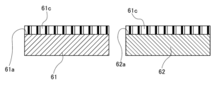
- Joining process 3-2. Insulating film formation As shown in FIG. 7, an insulating film 61c is formed on either or both of the bonding surface 61a of the first base material 61 and the bonding surface 62a of the second base material 62.
- an insulating film 61c is formed on both bonding surfaces 61a and 62a.
- the method for forming the insulating film 61c may be appropriately selected depending on the desired characteristics of the insulating film 61c, such as ion beam sputtering, ALD, magnetron sputtering, or CVD.
- the first base material 61 and the second base material 62 are bonded in a state where a certain concentration of the crosslinking substance 4 is present on either or both of the joint surfaces.
- 1 UV rays 5 are irradiated.
- the first ultraviolet ray 5 is irradiated on the insulating film 61c on both the bonding surface of the first base material 61 and the bonding surface of the second base material 62 in the presence of a constant concentration of the crosslinking substance 4. do.
- a precursor layer 61b is formed by irradiation with the first ultraviolet ray 5.
- This embodiment differs from the first embodiment in that an insulating film 61c is formed between the first base material 61 and the crosslinked layer 41 and between the second base material 62 and the crosslinked layer 41. be.
- Other steps are the same as in the first embodiment.
- the first ultraviolet ray 5 used in this embodiment may have a dominant wavelength of 156 nm, 172 nm, 185 nm, 206 nm, 222 nm, 254 nm, 283 nm, or 308 nm. .
- the material, structure, type of crosslinking substance, etc. of the first base material 61 and the second base material 62 are the same as those in the first embodiment.
- the insulating films 61c, 61c are formed on the bonding surfaces 61a, 62a, and the insulating films 61c, 61c are Precursor layers 61b, 61b are formed thereon. Since the first base material 61 and the second base material 62 are joined by joining the precursor layers 61b, 61b on these insulating films 61c, 61c, the precursor layers 61b, 61b made of the same material, The crosslinked layer 41 formed by the crosslinked layer 61b can be bonded relatively easily, and therefore the bonding strength between the first base material 61 and the second base material 62 can be improved.
- the fourth embodiment differs from the third embodiment in that, as shown in FIGS. 8 and 9, before forming the precursor layer 61b of the insulating film 61c, as shown in FIG.
- the second ultraviolet ray 8 is applied to one or both of the insulating film 61c on the bonding surface 61a side of the second base material 61 and the insulating film 61c on the bonding surface 62a side of the second base material 62.
- the second ultraviolet ray 8 is irradiated onto both the insulating films 61c, 61c.
- the steps other than this are the same as in the third embodiment.
- the surface condition is improved by removing moisture and impurities on the surface of the insulating film 61c before forming the precursor layer 61b.
- the bonding between the insulating film 61c and the precursor layer 61b and the film quality of the precursor layer 61b are improved, and as a result, the bonding strength between the first base material 61 and the second base material 62 is improved. can be improved.
- the second ultraviolet ray 8 may have a dominant wavelength of 156 nm, 172 nm, 185 nm, 206 nm, 222 nm, 254 nm, 283 nm, or 308 nm.
- the fifth embodiment differs from the third embodiment in that, as shown in FIG. 7, before forming the insulating film 61c, as shown in FIG. This is to irradiate one or both of the joint surfaces 62a of the base material 62 with the third ultraviolet rays 9.
- both the joint surface 61a of the first base material 61 and the joint surface 62a of the second base material 62 are irradiated with the third ultraviolet ray 9.
- the steps other than this are the same as in the third embodiment.
- the bonding surface 61a of the first base material 61 and the second base material 62 before the formation of the insulating film 61c are The surface condition of the surface with the bonding surface 62a is improved by removing moisture and impurities, etc., and the bonding between the first base material 61 and the insulating film 61c and the bonding between the second base material 62 and the insulating film 61c is performed. , and the film quality of the insulating films 61c, 61c are improved, and as a result, the bonding strength between the first base material 61 and the second base material 62 can be improved.
- the third ultraviolet ray 9 may have a dominant wavelength of 156 nm, 172 nm, 185 nm, 206 nm, 222 nm, 254 nm, 283 nm, or 308 nm.
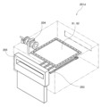
- FIG. 14 is a perspective view of a joining device 200 according to a sixth embodiment of the present invention. 17 to 22 are enlarged perspective views of main parts of the joining device 200.
- the bonding apparatus 200 includes chambers 201a to 201f whose atmospheric pressure can be freely controlled, an inert gas supply source 202 that supplies inert gas to the chambers 201a to 201f, and an ultraviolet irradiation mechanism 203 disposed within the chambers 201a, 201c, and 201d. , a crosslinking substance spraying mechanism 204 disposed within a chamber 201d, and a bonding mechanism 209 disposed within a chamber 201e.
- FIG. 15 shows a perspective view of the first base material 61 supported by the base material support 63.
- FIG. 16 shows a perspective view of the second base material 62 supported by the base material support 65.
- the chambers 201a to 201f are connected by a gate valve 205.
- the gate valve 205 allows the first base material 61 and the second base material 62 to be transported between the chambers 201a-201f while keeping each chamber 201a-201f airtight by opening and closing the gate.
- Each chamber 201a-201f is connected to an air pressure control source 215 via an air pressure control pipe 215a, and is connected to an inert gas supply source 202 via an inert gas supply pipe 202a.
- the atmospheric pressure control source 215 is constituted by, for example, a vacuum pump, an exhaust valve, etc., and freely controls the atmospheric pressure within each chamber 201a-201f.
- the inert gas supplied from the inert gas supply source 202 for example, nitrogen, helium, neon, argon, and a mixture of any combination thereof can be supplied to each chamber.
- nitrogen, helium, neon, argon, and a mixture of any combination thereof can be supplied to each chamber.
- the atmospheric pressure control source 215 is shown as being connected to each chamber 201a to 201f by an atmospheric pressure control pipe 215a, but each chamber 201a to 201f is independently connected to the atmospheric pressure control source 215. More specifically, an air pressure control source 215 is provided for each chamber 201a to 201f. Similarly, the supply of inert gas is performed independently for each chamber 201a-201f.
- the chamber 201a includes a gate valve 205 and an ultraviolet irradiation mechanism 203.
- the chamber 201a functions as a base material introduction and UV irradiation unit that introduces the base material into the bonding apparatus 200 and irradiates the bonding surface of the base materials 61 and 62 with ultraviolet rays.
- the chamber 201b includes a gate valve 205 and an ion beam sputtering mechanism 207.
- the chamber 201b functions as an ion beam sputtering section that forms a thin film on the joint surface of the base materials 61 and 62 by ion beam sputtering.
- the chamber 201c includes a gate valve 205 and an ultraviolet irradiation mechanism 203.
- the chamber 201c functions as a UV irradiation unit that irradiates the joint surface of the base materials 61 and 62 with ultraviolet rays.
- the chamber 201d includes a gate valve 205, an ultraviolet irradiation section 203, and a crosslinking substance spraying mechanism 204.
- the chamber 201d functions as a crosslinking substance spraying unit that sprays a crosslinking substance while irradiating the joint surface of the base materials 61 and 62 with ultraviolet rays.
- the chamber 201e includes a base material reversing mechanism 208 and a bonding mechanism 209.
- the base material reversing mechanism 208 includes a base material holding section 208a and a base material reversing section 208b.
- the joining mechanism 209 includes an upper pressing mechanism 209a, a lower pressing mechanism 209b, and a base material holding mechanism 209c.
- a substrate reversing mechanism 208 holds one substrate, inverts the other substrate and brings them into contact, and a bonding mechanism 209 joins the substrates 61 and 62. function as a department.
- the chamber 201f includes a gate valve 205.
- the chamber 201f functions as a base material unloading section that transports the joined base materials 61 and 62 to the outside of the joining apparatus 200.
- the first base material 61 is set in the chamber 201a (substrate introduction and UV irradiation section) with its joint surface facing downward.
- the gate valve 205 is closed, and after setting the chamber 201a to a desired atmosphere, the ultraviolet ray irradiation mechanism 203 irradiates the bonding surface of the first base material 61 with ultraviolet rays.
- the gate valve 205 is opened, the first base material 61 is transferred to the chamber 201b, and the gate valve 205 is closed.
- a second base material 62 is set in the same manner as the first base material 61, and is subjected to the same processing as the first base material.
- each chamber 201b-201f is set to a predetermined atmosphere.
- the first base material 61 transported to the chamber 201b (ion beam sputtering section) is passed over the upper part of the chamber 201b by the ion beam sputtering mechanism 207 while the inside of the chamber 201b is in a desired atmosphere. An insulating film is formed on the surface.
- the gate valve 205 is opened and the first base material 61 on which the insulating film has been formed is transported to the chamber 201c.
- the second base material 62 is transported to the chamber 201b and subjected to the same treatment as the first base material 61.
- the first base material 61 transported to the chamber 201c (UV irradiation unit) is irradiated with ultraviolet rays on its joint surface by the ultraviolet ray irradiation mechanism 203 while the inside of the chamber 201c is in a desired atmosphere.
- the first base material 61 that has been irradiated with ultraviolet light is transported to the chamber 201d with the gate valve 205 opened.
- the second base material 62 is transported to the chamber 201c and subjected to the same treatment as the first base material 61.
- the first base material 61 transported to the chamber 201d (crosslinking substance spraying section) is sprayed with a crosslinking substance into the chamber 201d by the crosslinking substance spraying mechanism 204 while the inside of the chamber 201d is in a desired atmosphere. .
- the bonding surface of the first base material 61 is irradiated with ultraviolet light by the ultraviolet irradiation mechanism 203 in a state where a certain concentration of the crosslinking substance is present on the bonding surface.
- the first base material 61 that has been irradiated with ultraviolet light is transported to the chamber 201e with the gate valve 205 opened.
- the second base material 62 is transported to the chamber 201e and subjected to the same treatment as the first base material 61.
- the first base material 61 conveyed to the chamber 201e (substrate joint part) is transferred to the base material holding part disposed above the base material reversing mechanism 208 while the inside of the chamber 201d is in a desired atmosphere. 208a and held there.
- a second base material 62 that has undergone the same treatment as the first material 61 is transported to the chamber 201e.
- the second base material 62 is held by the material reversing section 208b of the material reversing mechanism 208 and is inverted 180 degrees so that the joint surface of the second base material 62 faces upward.
- the first base material 61 held above is lowered to the position of the second base material 62, their joint surfaces are brought into contact with each other, and the joint surfaces are brought into contact with each other to be integrated, and then transported to the joining mechanism 209.
- a first material 61 and a second base material 62 that are integrated are held in a base material holding mechanism 209c, and an upper pressurizing mechanism 209a located above the upper pressurizing mechanism 209a and a lower pressurizing mechanism located below it. Pressure is applied from both the upper and lower directions by the mechanism 209b.
- the upper pressurizing mechanism 209a and the lower pressurizing mechanism 209b are provided with heaters (not shown) to obtain a desired bonded state depending on the type of the first material 61 and the second base material 62. is heated to the desired temperature.
- the first material 61 and the second base material 62 are contacted and pressurized via the precursor formed on their respective joint surfaces, Ultimately, it becomes a crosslinked layer, and the first material 61 and the second base material 62 are firmly joined by this crosslinked layer.
- the first material 61 and the second base material 62 which have been joined and become one body, are transported to the chamber 201f.
- the joined first base material 61 and second base material 62 that have been transported to the chamber 201f are returned to atmospheric pressure in the chamber 201d, and The bonding device 200 is carried out to the outside.
- the step of bonding the first base material 61 and the second base material 62 is sequentially performed in the chambers 201a to 201f in which the atmospheric pressure, moisture concentration, etc. are adjusted. be exposed.
- the bonding process consists of the following steps a) to f).
- the bonding apparatus 200 includes a chamber 201d that irradiates the bonding surface with ultraviolet rays while spraying the crosslinking substance with the crosslinking substance spraying mechanism 204, a precursor layer is formed on the bonding surface of the base materials 61 and 62, and this precursor layer is The base materials 61 and 62 can be firmly joined together at low temperature by the crosslinked layer formed by bringing the body layers into contact.
- step b) (champer 201b) may be omitted.
- the ultraviolet irradiation in steps a) and c) may be omitted depending on the type of base material and the bonding state. Since the bonding device 200 is configured by connecting a plurality of chambers 201a to 201f, it may be configured by removing unnecessary chambers by combining bonding processes.
- FIG. 23 is a cross-sectional view of a laminate 300 according to a seventh embodiment of the present invention.
- the method for forming the laminate 300 in this embodiment is the same as in the first embodiment.
- base materials 67, 67 in which an organic substance is coated on the circuit are used as the first base material and the second base material.
- a base material 67 having a circuit coated with an organic substance has a circuit layer 67b formed on a substrate 67a, and an organic substance 67c coated on the circuit of the circuit layer 67b.
- Other configuration functions are similar to those of the first embodiment, and have the same functions and effects as the first embodiment.
- the base materials 67 can be firmly bonded to each other at a low temperature by the crosslinked layer 41 adjacent to the organic substance 67a. Since bonding can be performed at low temperatures, a laminate can be formed without damaging the circuit.
- FIG. 24 is a cross-sectional view of a laminate 400 according to the eighth embodiment of the present invention.
- the method for forming the laminate 400 in this embodiment is the same as in the first embodiment.
- the difference is that base materials 69, 69 partially including conductive regions are used as the first base material and the second base material.
- the base material 69 partially including a conductive region has a conductive region 69b penetrating the circuit layer 69a and electrically connecting the circuit layers 69a to each other.
- Other configuration functions are similar to those of the first embodiment, and have the same functions and effects as the first embodiment.
- the crosslinked layer 41 can firmly join the base materials 69 to each other at a low temperature. Since bonding can be performed at low temperatures, a laminate can be formed without damaging the circuit. Further, the crosslinked layer 41 does not have a resistance so high as to inhibit electrical connection between the conductive regions 69b, so that the circuit layers 69a of the base material 69 can be electrically connected to each other.
- [Table 1] is a summary of the data obtained by irradiating VUV (172 nm/185 nm) on the bonding surface in the atmosphere and measuring the contact angle and bonding strength as a result of changes in irradiation time. The contact angle is measured as a parameter to confirm that OH, CHO, COOH, etc. are formed.
- Table 1 data was obtained for sample A without treatment, and then for samples B, C, D, and E, with different irradiation times of 60 sec, 120 sec, 180 sec, and 300 sec.
- a single 110W low-pressure mercury lamp used for VUV irradiation has an irradiation distance of 20 mm and an irradiation capacity of 30 mW/cm 2 or more at a wavelength of 254 nm and 5 mW/cm 2 or more at a wavelength of 185 nm.
- the contact angle decreases and the bonding strength increases by VUV irradiation.
- the irradiation time was 120 seconds or more, both the contact angle and the bonding strength reached a constant value, indicating that sufficient bonding strength was obtained.
Landscapes
- Engineering & Computer Science (AREA)
- Chemical & Material Sciences (AREA)
- Health & Medical Sciences (AREA)
- Organic Chemistry (AREA)
- Mechanical Engineering (AREA)
- Materials Engineering (AREA)
- Manufacturing & Machinery (AREA)
- Chemical Kinetics & Catalysis (AREA)
- Medicinal Chemistry (AREA)
- Polymers & Plastics (AREA)
- Toxicology (AREA)
- Microelectronics & Electronic Packaging (AREA)
- Laminated Bodies (AREA)
Abstract
Provided are: a method for bonding substrates containing polymers on the surfaces thereof; a bonding apparatus; and a laminate, applicable to high-frequency circuits in which substrates containing polymers on the surfaces thereof are firmly bonded with each other at low temperatures. The method for bonding substrates containing polymers on the surfaces thereof comprises: forming a precursor layer by radiating a first ultraviolet ray in a state in which a certain concentration of a crosslinking substance is present on one or both of the bonding surface of a first substrate 61 and the bonding surface of a second substrate 62; and bringing the first substrate and the second substrate into contact with each other to bond the first substrate 61 and the second substrate 62 via the precursor layer.
Description
本発明は、表面に重合体を含有する基材の接合方法、接合装置、および積層体に関する。
The present invention relates to a method for joining substrates containing a polymer on the surface, a joining device, and a laminate.
ポリイミド(PI)フィルムは優れた耐熱性、屈曲性、電気絶縁性から、フレキシブルプリント配線基板(FPC)の絶縁材料として用いられている。フレキシブルプリント配線基板の作製にはフレキシブル銅張積層板(FCCL)が用いられ、特にファイン回路形成を要求されるフレキシブルプリント配線基板においてはポリイミド表面のメタライズ方法の一つとして乾式法であるスパッタリング法が用いられている。
Polyimide (PI) film is used as an insulating material for flexible printed wiring boards (FPC) due to its excellent heat resistance, flexibility, and electrical insulation properties. Flexible copper clad laminates (FCCL) are used to manufacture flexible printed wiring boards, and sputtering, which is a dry method, is one of the methods for metalizing the polyimide surface, especially for flexible printed wiring boards that require fine circuit formation. It is used.
スマートフォンに代表される携帯情報端末などの小型化、高性能化に伴い、フレキシブルプリント配線基板の軽薄短小化、ファインパターン回路形成、低コスト化が強く望まれている。特に、フレキシブルプリント配線基板の基材として用いられる絶縁材料には、高周波回路に使用可能な材料が求められるが、高周波回路で良好な特性を有する材料は一般には高価であるため、製造コストが高くなるという課題がある。そこで、従来の材料をベースに、高周波回路で良好な特性を有する材料を接合した積層体を形成することが考察されている。したがって、これらの材料同士を低コストで強固に接合することが求められている。
With the miniaturization and higher performance of mobile information terminals such as smartphones, there is a strong demand for lighter, thinner, shorter and smaller flexible printed wiring boards, fine pattern circuit formation, and lower costs. In particular, insulating materials used as base materials for flexible printed wiring boards must be materials that can be used in high-frequency circuits, but materials that have good properties in high-frequency circuits are generally expensive, so manufacturing costs are high. There is an issue of becoming. Therefore, consideration has been given to forming a laminate based on conventional materials and joined with materials that have good characteristics in high-frequency circuits. Therefore, there is a need to firmly join these materials together at low cost.
一方、低温で高分子フィルムを接合して積層するために、有機系接着剤を用いる技術が開発されている(特許文献1)。有機系接着剤を用いる場合、真空などの特殊な環境下においては、時間の経過と共に、有機溶剤が最終製品の接着剤の層から蒸発するなどして抜けていくので、接合部の機械的強度の低下が起きる場合がある。また、バブルなどの欠陥が発生する恐れがあり、歩留まりが下がるので、最終コストを高める要因となる。
On the other hand, a technique using an organic adhesive has been developed to bond and laminate polymer films at low temperatures (Patent Document 1). When using organic adhesives, under special environments such as vacuum, the organic solvent evaporates from the adhesive layer of the final product over time, which reduces the mechanical strength of the joint. may occur. Furthermore, there is a risk that defects such as bubbles may occur, lowering the yield and increasing the final cost.
上述の問題を解決するために、本願発明は、表面に重合体を含有する基材同士を、低温で強固に接合する高周波回路で利用可能な、表面に重合体を含有する基材の接合方法、接合装置、および積層体を提供することを課題とする。
In order to solve the above-mentioned problems, the present invention provides a method for bonding substrates containing a polymer on the surface, which can be used in a high frequency circuit to firmly bond substrates containing a polymer on the surface at low temperatures. An object of the present invention is to provide a bonding device, and a laminate.
本発明は、上記課題を解決するため、以下の手段を採用する。
すなわち、本発明の表面に重合体を含有する基材を接合する方法は、第一の基材の接合面と、第二の基材の接合面と、のいずれか一方または双方に一定濃度の架橋物質が存在する状態で第一の紫外線を照射し前駆体層を形成すること、前記第一の基材と前記第二の基材とを当接させて、前記前駆体層を介して前記第一の基材と前記第二の基材とを接合すること、を含む。
この発明によれば、第一の基材の接合面と、第二の基材の接合面との、いずれか一方または双方に一定濃度の架橋物質が存在する状態で第一の紫外線を照射し前駆体層を形成するので、この前駆体層を介して第一の基材と第二の基材とを当接させることによって、第一の基材と第二の基材とを強固に接合することができる。 In order to solve the above problems, the present invention employs the following means.
That is, the method of bonding a substrate containing a polymer to the surface of the present invention involves applying a certain concentration to either or both of the bonding surface of the first substrate and the bonding surface of the second substrate. irradiating with a first ultraviolet ray in the presence of a crosslinking substance to form a precursor layer; bringing the first base material and the second base material into contact with each other to form a precursor layer through the precursor layer; The method includes joining the first base material and the second base material.
According to this invention, the first ultraviolet rays are irradiated in a state where a certain concentration of the crosslinking substance is present on either or both of the bonding surface of the first base material and the bonding surface of the second base material. Since a precursor layer is formed, the first base material and the second base material are brought into contact with each other through this precursor layer, thereby firmly joining the first base material and the second base material. can do.
本発明の別の側面の表面に重合体を含有する基材を接合する方法は、前記第一の基材の接合面と、前記第二の基材の接合面と、のいずれか一方または双方に絶縁膜を形成すること、前記第一の基材の接合面と、前記第二の基材の接合面と、のいずれか一方または双方に一定濃度の架橋物質が存在する状態で第一の紫外線を照射し前駆体層を形成すること、前記第一の基材と前記第二の基材とを当接させて、前記前駆体層を介して前記第一の基材と前記第二の基材とを接合すること、を含む。
この発明によれば、第一の基材の接合面と、第二の基材の接合面との、いずれか一方または双方に絶縁膜が形成され、さらに、第一の基材の接合面と、第二の基材の接合面との、いずれか一方または双方に前駆体層を形成するので、この前駆体層を介して第一の基材と第二の基材とを当接させることによって、第一の基材と第二の基材とをさらに強固に接合することができる。 Another aspect of the present invention is a method for bonding a base material containing a polymer to a surface of the first base material and/or both of the bonding surface of the first base material and the bonding surface of the second base material. forming an insulating film on the bonding surface of the first base material and the bonding surface of the second base material in a state where a certain concentration of a crosslinking substance is present on either or both of the bonding surface of the first base material and the bonding surface of the second base material; irradiating ultraviolet rays to form a precursor layer, bringing the first base material and the second base material into contact with each other, and forming the first base material and the second base material through the precursor layer; This includes joining the base material.
According to this invention, an insulating film is formed on one or both of the bonding surface of the first base material and the bonding surface of the second base material, and further, the insulating film is formed on the bonding surface of the first base material and the bonding surface of the second base material. , a precursor layer is formed on one or both of the bonding surfaces of the second base material, so that the first base material and the second base material are brought into contact via this precursor layer. This allows the first base material and the second base material to be joined more firmly.
本発明の一態様では、前記前駆体層を形成することの前に、前記第一の基材の接合面と、前記第二の基材の接合面と、のいずれか一方または双方に第二の紫外線を照射すること、
を含む。
この一態様では、前躯体層を形成する前に、第一の基材の接合面と第二の基材の接合面と、のいずれか一方または双方に第二の紫外線を照射するので、前駆体層を形成する面を清浄にすることができる。 In one aspect of the present invention, before forming the precursor layer, a second base material is applied to one or both of the bonding surface of the first base material and the bonding surface of the second base material. irradiating with ultraviolet rays,
including.
In this embodiment, before forming the precursor layer, one or both of the bonding surface of the first base material and the bonding surface of the second base material is irradiated with the second ultraviolet rays. The surface on which the body layer is formed can be cleaned.
本発明の一態様では、前記絶縁膜を形成することの前に、前記第一の基材の接合面と、前記第二の基材の接合面と、のいずれか一方または双方に第三の紫外線を照射すること、
を含む。
この一態様では、絶縁膜を形成する前に、第一の基材の接合面と、第二の基材の接合面と、のいずれか一方または双方に第三の紫外線を照射するので、絶縁膜を形成する面を清浄にすることができる。 In one aspect of the present invention, before forming the insulating film, a third bonding surface is applied to one or both of the bonding surface of the first base material and the bonding surface of the second base material. irradiating with ultraviolet light,
including.
In this aspect, before forming the insulating film, either or both of the bonding surface of the first base material and the bonding surface of the second base material is irradiated with the third ultraviolet rays, so that the insulating film can be insulated. The surface on which the film is to be formed can be cleaned.
本発明の一態様では、前記前駆体層を形成すること、前記接合することは、酸素濃度、水分濃度の制御された環境下で行われる。
この一態様では、前駆体層の形成と、接合とが、酸素濃度、水分濃度の制御された環境下で行われるので、それぞれの工程ごとに適した環境を整えることができる。 In one aspect of the present invention, forming the precursor layer and bonding are performed in an environment with controlled oxygen concentration and water concentration.
In this embodiment, the formation of the precursor layer and the bonding are performed in an environment where the oxygen concentration and water concentration are controlled, so that an environment suitable for each step can be prepared.
本発明の一態様では、前記酸素濃度、水分濃度の制御は、真空、または不活性気体雰囲気中で行われる。
この一態様では、真空、または不活性気体雰囲気中で酸素濃度、水分濃度の制御が行われるので、酸素濃度、水分濃度の制御のための適切な環境を作ることができる。 In one aspect of the present invention, the oxygen concentration and water concentration are controlled in vacuum or in an inert gas atmosphere.
In this embodiment, the oxygen concentration and moisture concentration are controlled in a vacuum or an inert gas atmosphere, so that an appropriate environment for controlling the oxygen concentration and moisture concentration can be created.
本発明の一態様では、前記第一、第二の基材が、LCP(液晶ポリマー),PFA(テトラフルオロエチレン・パーフルオロアルキルビニルエーテル共重合体),PTFE(ポリテトラフルオロエチレン)、COP(シクロオレフィンポリマー),PPS(ポリフェニレンスルフィド)、PEEK(ポリエーテルエーテルケトン)、PI系(PI(ポリイミド)、MPI(変性ポリイミド)を含む)、PPE系(PPE(ポリフェニレンエーテル)、mPPE(変性ポリフェニレンエーテル)を含む)のいずれかの高分子フィルム、グラファイトシート、またはこれらの組合せの積層体である。
この一態様では、基材の材料として適切なものを選択できる。 In one aspect of the present invention, the first and second base materials include LCP (liquid crystal polymer), PFA (tetrafluoroethylene perfluoroalkyl vinyl ether copolymer), PTFE (polytetrafluoroethylene), COP (cyclo Olefin polymer), PPS (polyphenylene sulfide), PEEK (polyether ether ketone), PI system (including PI (polyimide), MPI (modified polyimide)), PPE system (PPE (polyphenylene ether), mPPE (modified polyphenylene ether)) ), a graphite sheet, or a laminate of a combination thereof.
In this embodiment, an appropriate material can be selected for the base material.
本発明の一態様では、前記第一、第二の基材が、回路上に有機物質を塗工した基材である。
この一態様では、回路を有する基材であっても、塗工された有機物質を介して上述と同様の方法で積層体を形成することができる。 In one aspect of the present invention, the first and second base materials are base materials having a circuit coated with an organic substance.
In this embodiment, even if the base material has a circuit, a laminate can be formed in the same manner as described above using a coated organic substance.
本発明の一態様では、前記第一、第二の基材が、表面の少なくとも一部に導電性の領域を含む基材である。
この一態様では、表面の少なくとも一部に導電性の領域を含む基材を接合するので、基材の回路同士を連結した積層体を形成することができる。 In one aspect of the present invention, the first and second base materials are base materials that include a conductive region on at least a portion of the surface.
In this embodiment, since the base materials including a conductive region on at least a portion of the surface are bonded, it is possible to form a laminate in which circuits of the base materials are connected to each other.
本発明の一態様では、前記架橋物質がアンモニア、第1級アルコール、第2級アルコールからなる群から選択されるいずれかまたはいずれかの組合せである。
この一態様では、架橋物質として適切なものを選択することができる。 In one aspect of the invention, the crosslinking substance is any one or any combination selected from the group consisting of ammonia, primary alcohols, and secondary alcohols.
In this embodiment, a suitable crosslinking material can be selected.
この一態様では、架橋物質として適切なものを選択することができる。 In one aspect of the invention, the crosslinking substance is any one or any combination selected from the group consisting of ammonia, primary alcohols, and secondary alcohols.
In this embodiment, a suitable crosslinking material can be selected.
本発明の一態様では、前記第一の紫外線、前記第二の紫外線、前記第三の紫外線は、主波長が156nm、172nm、185nm、206nm、222nm、254nm、283nm、308nm、のいずれかまたはいずれかの組合せである。
この一態様では、第一の紫外線、第二の紫外線、第三の紫外線として、適切な主波長のものを選択できる。 In one aspect of the present invention, the first ultraviolet ray, the second ultraviolet ray, and the third ultraviolet ray have a main wavelength of 156 nm, 172 nm, 185 nm, 206 nm, 222 nm, 254 nm, 283 nm, or 308 nm. It is a combination of these.
In this embodiment, appropriate main wavelengths can be selected as the first ultraviolet ray, the second ultraviolet ray, and the third ultraviolet ray.
本発明の接合装置は、気圧制御自在なチャンバと、前記チャンバへ不活性気体を供給する不活性気体供給管と、前記チャンバ内に配置される、紫外線照射機構と、架橋物質噴霧機構と、接合機構と、を備える。
この発明によれば、表面に重合体を含有する基材同士を、低温で強固に接合することができる接合装置を提供することができる。 The bonding apparatus of the present invention includes a chamber that can freely control the atmospheric pressure, an inert gas supply pipe that supplies an inert gas to the chamber, an ultraviolet irradiation mechanism, a crosslinking substance spraying mechanism, and a crosslinking substance spraying mechanism that are arranged in the chamber. A mechanism.
According to the present invention, it is possible to provide a bonding device that can firmly bond substrates containing polymers on their surfaces at low temperatures.
表面に重合体を含有する第一の基材と、架橋層と、表面に重合体を含有する第二の基材と、をこの順に積層する積層体。
この発明によれば、表面に重合体を含有する基材同士を接合し、高周波回路で利用可能な積層体を提供することができる。 A laminate in which a first base material containing a polymer on the surface, a crosslinked layer, and a second base material containing a polymer on the surface are laminated in this order.
According to the present invention, it is possible to provide a laminate that can be used in a high frequency circuit by bonding base materials containing a polymer on the surface.
本願発明によれば、表面に重合体を含有する基材同士を、低温で強固に接合する高周波回路で利用可能な、表面に重合体を含有する基材の接合方法、接合装置、および積層体を提供することができる。
According to the present invention, there is provided a joining method, a joining device, and a laminate for substrates containing a polymer on the surface, which can be used in a high-frequency circuit that firmly joins substrates containing a polymer on the surface at low temperatures. can be provided.
<第1実施形態>
図1から図5は、本発明の第1実施形態に係る第一の基材と第二の基材との接合工程を説明する模式図である。これらの図を参照して、本実施形態に係る第一の基材と第二の基材との接合工程を説明する。
(接合工程1-1.第一の基材と第二の基材の準備)
図1に示すように、表面に重合体を含有する第一の基材61と第二の基材62を準備する。 <First embodiment>
FIGS. 1 to 5 are schematic diagrams illustrating a process of joining a first base material and a second base material according to the first embodiment of the present invention. With reference to these figures, the process of joining the first base material and the second base material according to the present embodiment will be described.
(Joining process 1-1. Preparation of first base material and second base material)
As shown in FIG. 1, afirst base material 61 and a second base material 62 containing a polymer on their surfaces are prepared.
図1から図5は、本発明の第1実施形態に係る第一の基材と第二の基材との接合工程を説明する模式図である。これらの図を参照して、本実施形態に係る第一の基材と第二の基材との接合工程を説明する。
(接合工程1-1.第一の基材と第二の基材の準備)
図1に示すように、表面に重合体を含有する第一の基材61と第二の基材62を準備する。 <First embodiment>
FIGS. 1 to 5 are schematic diagrams illustrating a process of joining a first base material and a second base material according to the first embodiment of the present invention. With reference to these figures, the process of joining the first base material and the second base material according to the present embodiment will be described.
(Joining process 1-1. Preparation of first base material and second base material)
As shown in FIG. 1, a
(接合工程1-2.紫外線による前駆体層の形成)
次いで、図2に示すように、第一の基材61の接合面61aと、第二の基材62の接合面62aと、のいずれか一方または双方に一定濃度の架橋物質4が存在する状態で第一の紫外線5を照射する。本実施形態では、第一の基材61の接合面61aと第二の基材62の接合面62aの双方において、一定濃度の架橋物質4が存在する状態で第一の紫外線5を照射する。図3に示すように、この第一の紫外線5の照射によって、双方の基材61、62表面に前駆体層61a、61aが形成される。 (Joining process 1-2. Formation of precursor layer using ultraviolet rays)
Next, as shown in FIG. 2, a state in which a certain concentration of thecrosslinking substance 4 is present on either or both of the bonding surface 61a of the first base material 61 and the bonding surface 62a of the second base material 62. irradiate with the first ultraviolet light 5. In this embodiment, the first ultraviolet ray 5 is irradiated on both the bonding surface 61a of the first base material 61 and the bonding surface 62a of the second base material 62 in a state where a certain concentration of the crosslinking substance 4 is present. As shown in FIG. 3, by irradiation with the first ultraviolet ray 5, precursor layers 61a, 61a are formed on the surfaces of both base materials 61, 62.
次いで、図2に示すように、第一の基材61の接合面61aと、第二の基材62の接合面62aと、のいずれか一方または双方に一定濃度の架橋物質4が存在する状態で第一の紫外線5を照射する。本実施形態では、第一の基材61の接合面61aと第二の基材62の接合面62aの双方において、一定濃度の架橋物質4が存在する状態で第一の紫外線5を照射する。図3に示すように、この第一の紫外線5の照射によって、双方の基材61、62表面に前駆体層61a、61aが形成される。 (Joining process 1-2. Formation of precursor layer using ultraviolet rays)
Next, as shown in FIG. 2, a state in which a certain concentration of the
(接合工程1-3.第一の基材と第二の基材の接合)
前駆体層61b、61bが形成された第一の基材61と第二の基材62とを、図4に示すように前駆体層61b、61bが対向するように当接させる。図5に示すように、前駆体層61b、61bが接触することにより、架橋層41が形成され、第一の基材61と第二の基材62とが架橋層41により接合される。かくして、第一の基材61、架橋層41、第二の基材62がこの順に積層する積層体1を得ることができる。本工程の接合に際し、この積層体1を加熱してもよい、加熱することによって、接合強度をさらに向上することができる。 (Joining process 1-3. Joining of first base material and second base material)
Thefirst base material 61 and the second base material 62 on which the precursor layers 61b, 61b are formed are brought into contact with each other so that the precursor layers 61b, 61b face each other, as shown in FIG. As shown in FIG. 5, a crosslinked layer 41 is formed by the contact between the precursor layers 61b and 61b, and the first base material 61 and the second base material 62 are joined by the crosslinked layer 41. In this way, it is possible to obtain a laminate 1 in which the first base material 61, the crosslinked layer 41, and the second base material 62 are laminated in this order. During the bonding in this step, the laminate 1 may be heated, and by heating, the bonding strength can be further improved.
前駆体層61b、61bが形成された第一の基材61と第二の基材62とを、図4に示すように前駆体層61b、61bが対向するように当接させる。図5に示すように、前駆体層61b、61bが接触することにより、架橋層41が形成され、第一の基材61と第二の基材62とが架橋層41により接合される。かくして、第一の基材61、架橋層41、第二の基材62がこの順に積層する積層体1を得ることができる。本工程の接合に際し、この積層体1を加熱してもよい、加熱することによって、接合強度をさらに向上することができる。 (Joining process 1-3. Joining of first base material and second base material)
The
(工程環境)
前駆体層61bを形成すること、第一の基材61と第二の基材62とを接合することは、酸素濃度、水分濃度の制御された環境下で行われる。この酸素濃度、水分濃度の制御は、真空、または窒素雰囲気中で行われてよい。あるいは、窒素に替えて、他の不活性気体を選択してもよい。不活性気体としては、例えば、窒素、ヘリウム、ネオン、アルゴン、及び、これらのいずれかの組み合わせの混合物を選択してよい。 (Process environment)
Forming theprecursor layer 61b and bonding the first base material 61 and the second base material 62 are performed in an environment with controlled oxygen concentration and water concentration. This control of oxygen concentration and moisture concentration may be performed in vacuum or in a nitrogen atmosphere. Alternatively, other inert gases may be selected instead of nitrogen. As the inert gas, for example, mixtures of nitrogen, helium, neon, argon, and any combination thereof may be selected.
前駆体層61bを形成すること、第一の基材61と第二の基材62とを接合することは、酸素濃度、水分濃度の制御された環境下で行われる。この酸素濃度、水分濃度の制御は、真空、または窒素雰囲気中で行われてよい。あるいは、窒素に替えて、他の不活性気体を選択してもよい。不活性気体としては、例えば、窒素、ヘリウム、ネオン、アルゴン、及び、これらのいずれかの組み合わせの混合物を選択してよい。 (Process environment)
Forming the
(第一の基材、第二の基材)
本実施形態においては、第一の基材61、第二の基材62は、LCP(液晶ポリマー),PFA(テトラフルオロエチレン・パーフルオロアルキルビニルエーテル共重合体),PTFE(ポリテトラフルオロエチレン)、COP(シクロオレフィンポリマー),PPS(ポリフェニレンスルフィド)、PEEK(ポリエーテルエーテルケトン)、PI系(PI(ポリイミド)、MPI(変性ポリイミド)を含む)、PPE系(PPE(ポリフェニレンエーテル)、mPPE(変性ポリフェニレンエーテル)を含む)のいずれかの高分子フィルム、グラファイトシート、またはこれらの組合せの積層体であってよい。これらの材料は、所望の高周波回路特性、ガス透過特性、防湿特性等に基づいて選択してよい。本発明の重合体には、高分子フィルムのほか、該フィルムを高温で焼結させたグラファイトシートも含まれる。 (First base material, second base material)
In this embodiment, thefirst base material 61 and the second base material 62 are LCP (liquid crystal polymer), PFA (tetrafluoroethylene perfluoroalkyl vinyl ether copolymer), PTFE (polytetrafluoroethylene), COP (cycloolefin polymer), PPS (polyphenylene sulfide), PEEK (polyether ether ketone), PI system (including PI (polyimide), MPI (modified polyimide)), PPE system (PPE (polyphenylene ether), mPPE (modified) (including polyphenylene ether), graphite sheets, or laminates of combinations thereof. These materials may be selected based on desired high frequency circuit properties, gas permeation properties, moisture proof properties, etc. The polymer of the present invention includes not only a polymer film but also a graphite sheet obtained by sintering the film at high temperature.
本実施形態においては、第一の基材61、第二の基材62は、LCP(液晶ポリマー),PFA(テトラフルオロエチレン・パーフルオロアルキルビニルエーテル共重合体),PTFE(ポリテトラフルオロエチレン)、COP(シクロオレフィンポリマー),PPS(ポリフェニレンスルフィド)、PEEK(ポリエーテルエーテルケトン)、PI系(PI(ポリイミド)、MPI(変性ポリイミド)を含む)、PPE系(PPE(ポリフェニレンエーテル)、mPPE(変性ポリフェニレンエーテル)を含む)のいずれかの高分子フィルム、グラファイトシート、またはこれらの組合せの積層体であってよい。これらの材料は、所望の高周波回路特性、ガス透過特性、防湿特性等に基づいて選択してよい。本発明の重合体には、高分子フィルムのほか、該フィルムを高温で焼結させたグラファイトシートも含まれる。 (First base material, second base material)
In this embodiment, the
(架橋物質)
紫外線照射時に存在する架橋物質としては、アンモニア、第1級アルコール、第2級アルコールからなる群から選択されるいずれかまたはいずれかの組合せであってよい。紫外線照射時のこれらの架橋物質は、ガス状であってもよく、霧状(の液滴)であってもよく、これらの混合物であってもよい。上記のアルコール化合物としては、後述する接合の作用のため、紫外線を照射した際に、ヒドロキシラジカル、及び、CHラジカルが生じやすく、結果としてカルボキシ基を生じさせやすくなると考えられるものがよい。特に上記アルコール化合物の炭素数は1~5個であることが好ましい。そのようなアルコール化合物としては、メタノール、エタノール、1-プロパノール、1-ブタノール、1-ペンタノール、2-プロパノール、2-ブタノール、2ーペンタノール、イソブチルアルコール、イソアミルアルコール、tert-ブチルアルコール、及び、tert-アミルアルコールが挙げられる。なかでも、炭素数1~5個の第1級アルコールが好ましく、また、有害性がより低い(ヒトの体内において有害なホルムアルデヒド、及び、ギ酸等を生じにくい)点で、炭素数2~5個の第1級アルコールがより好ましく、エタノール、1-プロパノール、1-ブタノール、又は、1-ペンタノールが更に好ましく、エタノール、及び、1-プロパノールが特に好ましく、エタノールが最も好ましい。 (Crosslinked substance)
The crosslinking substance present during ultraviolet irradiation may be any one selected from the group consisting of ammonia, primary alcohols, and secondary alcohols, or any combination thereof. These crosslinked substances upon irradiation with ultraviolet rays may be in a gaseous state, a mist (droplets), or a mixture thereof. The above-mentioned alcohol compound is preferably one that is considered to be likely to generate hydroxyl radicals and CH radicals when irradiated with ultraviolet rays due to the bonding action described below, and as a result, to easily generate carboxyl groups. In particular, the alcohol compound preferably has 1 to 5 carbon atoms. Such alcohol compounds include methanol, ethanol, 1-propanol, 1-butanol, 1-pentanol, 2-propanol, 2-butanol, 2-pentanol, isobutyl alcohol, isoamyl alcohol, tert-butyl alcohol, and tert-butyl alcohol. - Examples include amyl alcohol. Among these, primary alcohols having 1 to 5 carbon atoms are preferable, and primary alcohols having 2 to 5 carbon atoms are preferred because they are less harmful (hardly producing harmful formaldehyde, formic acid, etc. in the human body). More preferred are primary alcohols, ethanol, 1-propanol, 1-butanol, or 1-pentanol are even more preferred, ethanol and 1-propanol are particularly preferred, and ethanol is most preferred.
(紫外線)
一定濃度の架橋物質が存在する状態で照射される紫外線は、主波長が156nm、172nm、185nm、206nm、222nm、254nm、283nm、308nm、のいずれかであってよい。これらの波長を含む紫外線源としては、低圧水銀ランプ、高圧水銀ランプ、エキシマランプ、深紫外LED等、所望の波長を有するものを適宜選択できる。 (ultraviolet light)
The ultraviolet rays irradiated in the presence of a certain concentration of the crosslinking substance may have a dominant wavelength of 156 nm, 172 nm, 185 nm, 206 nm, 222 nm, 254 nm, 283 nm, or 308 nm. As the ultraviolet source including these wavelengths, one having a desired wavelength can be appropriately selected, such as a low-pressure mercury lamp, a high-pressure mercury lamp, an excimer lamp, and a deep ultraviolet LED.
(前駆体層および架橋層)
第一の基材61、第二の基材62の前駆体層61bとしては、例えば、基材61、62がポリイミドの場合は、下記[化1]に示すように架橋性重合体を含有する構造を有している。図中破線R-Rは、基材61、62の表面近傍を表している。図中Aの終端は、-C(=O)-O-H、又は-CH3を表す。 (Precursor layer and crosslinked layer)
For example, when the base materials 61 and 62 are polyimide, the precursor layer 61b of the first base material 61 and the second base material 62 contains a crosslinkable polymer as shown in [Chemical formula 1] below. It has a structure. The broken line RR in the figure represents the vicinity of the surfaces of the base materials 61 and 62. In the figure, the terminal end of A represents -C(=O)-OH or -CH 3 .
第一の基材61、第二の基材62の前駆体層61bとしては、例えば、基材61、62がポリイミドの場合は、下記[化1]に示すように架橋性重合体を含有する構造を有している。図中破線R-Rは、基材61、62の表面近傍を表している。図中Aの終端は、-C(=O)-O-H、又は-CH3を表す。 (Precursor layer and crosslinked layer)
For example, when the

[化1]に示すようにアルキル鎖架橋の終端の多くは、-C(=O)-O-H、又は-CH3となっている。下記[化2](A-1)示す通り、一方の端部Dと他方の端部Eが近接した時に、H2Oが離脱し、O原子を介してその両端が結合する(B-1)。また、(A-2)に示すように、CH3基の場合も他方からやってきたOH基と結合し、同様にH2Oが離脱し、O原子を介してその両端が結合する(B-1)。式中破線は、水素結合を表している。式(B-1)の酸素Oによる結合は、加水分解され得るが、それらは、-C(=O)-O-H、又は-CH3に分解されるので、可逆的である。したがって、分解が生じた場合でも同時に再結合が起こり、相互の結合は維持される。
As shown in [Chemical Formula 1], most of the terminal ends of the alkyl chain crosslinks are -C(=O)-OH or -CH 3 . As shown in [Chemical Formula 2] (A-1) below, when one end D and the other end E come close to each other, H 2 O is separated and the two ends are bonded via the O atom (B-1 ). Furthermore, as shown in (A-2), in the case of CH 3 group, it also bonds with the OH group coming from the other side, H 2 O leaves in the same way, and both ends bond through the O atom (B- 1). The dashed line in the formula represents a hydrogen bond. Although the bonds with oxygen O in formula (B-1) can be hydrolyzed, they are reversible since they are decomposed to -C(=O)-O-H, or -CH 3 . Therefore, even if decomposition occurs, recombination occurs at the same time, and mutual bonds are maintained.

以上述べたように、本実施形態における表面に重合体を含有する第一の基材と第二の基材との接合方法では、アンモニア、第1級アルコール、第2級アルコールからなる群から選択されるいずれかまたはいずれかの組合せである架橋物質が一定濃度で存在する状態で紫外線を照射し、前駆体層を形成する。これらの前駆体層を当接することによって、架橋層を形成し、この架橋層を介して第一の基材と第二の基材とを接合するので、第一の基材と第二の基材とを低温で強固に接合する接合方法を提供できる。第一の基材、第二の基材は、LCP(液晶ポリマー),PFA(テトラフルオロエチレン・パーフルオロアルキルビニルエーテル共重合体),PTFE(ポリテトラフルオロエチレン)、COP(シクロオレフィンポリマー),PPS(ポリフェニレンスルフィド)、PEEK(ポリエーテルエーテルケトン)、PI系(PI(ポリイミド)、MPI(変性ポリイミド)を含む)、PPE系(PPE(ポリフェニレンエーテル)、mPPE(変性ポリフェニレンエーテル)を含む)のいずれかの高分子フィルム、グラファイトシート、またはこれらの組合せの積層体から選択できるので、高周波回路で利用可能なものを適宜選択できる。したがって、第一の基材と第二の基材とを低温で強固に接合する高周波回路で利用可能な表面に重合体を含有する基材同士の接合方法を提供することができる。
As described above, in the method of joining the first base material and the second base material containing a polymer on the surface in this embodiment, a selected alcohol is selected from the group consisting of ammonia, primary alcohol, and secondary alcohol. A precursor layer is formed by irradiating ultraviolet rays in the presence of a certain concentration of a crosslinking material or a combination thereof. By bringing these precursor layers into contact, a cross-linked layer is formed, and the first base material and the second base material are bonded via this cross-linked layer. It is possible to provide a joining method that firmly joins materials at low temperatures. The first base material and the second base material are LCP (liquid crystal polymer), PFA (tetrafluoroethylene perfluoroalkyl vinyl ether copolymer), PTFE (polytetrafluoroethylene), COP (cycloolefin polymer), PPS. Any of the following: Since the material can be selected from a polymer film, a graphite sheet, or a laminate of a combination thereof, it is possible to appropriately select one that can be used in a high frequency circuit. Therefore, it is possible to provide a method for joining base materials whose surfaces contain a polymer, which can be used in a high frequency circuit that firmly joins a first base material and a second base material at low temperatures.
<第2実施形態>
次に、本発明の第2実施形態について説明する。第2実施形態が第1実施形態と異なるのは、図2、図3に示す、第一の基材61、第二の基材62の前駆体層61b、61bを形成することの前に、図6に示すように、第一の基材61の接合面61aと、第二の基材62の接合面62aとのいずれか一方または双方に第二の紫外線8を照射することである。本実施形態では、第一の基材61の接合面61aと、第二の基材62の接合面62aとの双方に第二の紫外線8を照射する。これ以外の工程は、第1実施形態と同様である。第1実施形態に加え、この工程が追加されることによって、第1実施形態の作用効果に加え、前駆体層61b、61bの形成前の第一の基材61の接合面61aと、第二の基材62の接合面62aの表面の水分や不純物の除去等による表面状態の改善が行われ、第一の基材61と前駆体層61bと、および第二の基材62と前駆体層61bとの結合、および前駆体層61b、61bの膜質が改善され、結果として、第一の基材61と第二の基材62との接合強度を向上することができる。なお、第二の紫外線8としては、主波長が156nm、172nm、185nm、206nm、222nm、254nm、283nm、308nm、のいずれかであってよい。 <Second embodiment>
Next, a second embodiment of the present invention will be described. The second embodiment differs from the first embodiment in that, as shown in FIGS. 2 and 3, before forming the precursor layers 61b and 61b of thefirst base material 61 and the second base material 62, As shown in FIG. 6, one or both of the bonding surface 61a of the first base material 61 and the bonding surface 62a of the second base material 62 is irradiated with second ultraviolet rays 8. In this embodiment, both the bonding surface 61a of the first base material 61 and the bonding surface 62a of the second base material 62 are irradiated with the second ultraviolet rays 8. The steps other than this are the same as those in the first embodiment. In addition to the first embodiment, by adding this step, in addition to the effects of the first embodiment, the bonding surface 61a of the first base material 61 before the formation of the precursor layers 61b, 61b, and the second The surface condition of the joint surface 62a of the base material 62 is improved by removing moisture and impurities from the surface, and the first base material 61 and the precursor layer 61b, and the second base material 62 and the precursor layer 61b and the film quality of the precursor layers 61b, 61b are improved, and as a result, the bonding strength between the first base material 61 and the second base material 62 can be improved. Note that the second ultraviolet ray 8 may have a dominant wavelength of 156 nm, 172 nm, 185 nm, 206 nm, 222 nm, 254 nm, 283 nm, or 308 nm.
次に、本発明の第2実施形態について説明する。第2実施形態が第1実施形態と異なるのは、図2、図3に示す、第一の基材61、第二の基材62の前駆体層61b、61bを形成することの前に、図6に示すように、第一の基材61の接合面61aと、第二の基材62の接合面62aとのいずれか一方または双方に第二の紫外線8を照射することである。本実施形態では、第一の基材61の接合面61aと、第二の基材62の接合面62aとの双方に第二の紫外線8を照射する。これ以外の工程は、第1実施形態と同様である。第1実施形態に加え、この工程が追加されることによって、第1実施形態の作用効果に加え、前駆体層61b、61bの形成前の第一の基材61の接合面61aと、第二の基材62の接合面62aの表面の水分や不純物の除去等による表面状態の改善が行われ、第一の基材61と前駆体層61bと、および第二の基材62と前駆体層61bとの結合、および前駆体層61b、61bの膜質が改善され、結果として、第一の基材61と第二の基材62との接合強度を向上することができる。なお、第二の紫外線8としては、主波長が156nm、172nm、185nm、206nm、222nm、254nm、283nm、308nm、のいずれかであってよい。 <Second embodiment>
Next, a second embodiment of the present invention will be described. The second embodiment differs from the first embodiment in that, as shown in FIGS. 2 and 3, before forming the precursor layers 61b and 61b of the
<第3実施形態>
図1、および図7から図11は、本発明の第3実施形態に係る第一の基材と第二の基材との接合工程を説明する模式図である。これらの図を参照して、本実施形態に係る第一の基材と第二の基材との接合工程を説明する。
(接合工程3-1.第一の基材と第二の基材の準備)
図1に示すように、第一の基材61と第二の基材62を準備する。
(接合工程3-2.絶縁膜形成)
図7に示すように第一の基材61の接合面61a、第二の基材62の接合面62aのいずれか又は双方に絶縁膜61cを形成する。本実施形態では、双方の接合面61a、62aに絶縁膜61cを形成する。絶縁膜61cの形成法としては、イオンビームスパッタ法、ALD法、マグネトロンスパッタ法、CVD法等適宜絶縁膜61cの所望の特性に応じて選択してよい。 <Third embodiment>
FIG. 1 and FIGS. 7 to 11 are schematic diagrams illustrating a process of joining a first base material and a second base material according to a third embodiment of the present invention. With reference to these figures, the process of joining the first base material and the second base material according to the present embodiment will be described.
(Joining process 3-1. Preparation of first base material and second base material)
As shown in FIG. 1, afirst base material 61 and a second base material 62 are prepared.
(Joining process 3-2. Insulating film formation)
As shown in FIG. 7, an insulatingfilm 61c is formed on either or both of the bonding surface 61a of the first base material 61 and the bonding surface 62a of the second base material 62. In this embodiment, an insulating film 61c is formed on both bonding surfaces 61a and 62a. The method for forming the insulating film 61c may be appropriately selected depending on the desired characteristics of the insulating film 61c, such as ion beam sputtering, ALD, magnetron sputtering, or CVD.
図1、および図7から図11は、本発明の第3実施形態に係る第一の基材と第二の基材との接合工程を説明する模式図である。これらの図を参照して、本実施形態に係る第一の基材と第二の基材との接合工程を説明する。
(接合工程3-1.第一の基材と第二の基材の準備)
図1に示すように、第一の基材61と第二の基材62を準備する。
(接合工程3-2.絶縁膜形成)
図7に示すように第一の基材61の接合面61a、第二の基材62の接合面62aのいずれか又は双方に絶縁膜61cを形成する。本実施形態では、双方の接合面61a、62aに絶縁膜61cを形成する。絶縁膜61cの形成法としては、イオンビームスパッタ法、ALD法、マグネトロンスパッタ法、CVD法等適宜絶縁膜61cの所望の特性に応じて選択してよい。 <Third embodiment>
FIG. 1 and FIGS. 7 to 11 are schematic diagrams illustrating a process of joining a first base material and a second base material according to a third embodiment of the present invention. With reference to these figures, the process of joining the first base material and the second base material according to the present embodiment will be described.
(Joining process 3-1. Preparation of first base material and second base material)
As shown in FIG. 1, a
(Joining process 3-2. Insulating film formation)
As shown in FIG. 7, an insulating
(接合工程3-3.紫外線の照射)
次いで、図8に示すように、第一の基材61の接合面と、第二の基材62の接合面と、のいずれか一方または双方に一定濃度の架橋物質4が存在する状態で第一の紫外線5を照射する。本実施形態では、第一の基材61の接合面と第二の基材62の接合面双方の絶縁膜61c上において、一定濃度の架橋物質4が存在する状態で第一の紫外線5を照射する。図9に示すように、この第一の紫外線5の照射によって、前駆体層61bが形成される。 (Joining process 3-3. Ultraviolet irradiation)
Next, as shown in FIG. 8, thefirst base material 61 and the second base material 62 are bonded in a state where a certain concentration of the crosslinking substance 4 is present on either or both of the joint surfaces. 1 UV rays 5 are irradiated. In this embodiment, the first ultraviolet ray 5 is irradiated on the insulating film 61c on both the bonding surface of the first base material 61 and the bonding surface of the second base material 62 in the presence of a constant concentration of the crosslinking substance 4. do. As shown in FIG. 9, a precursor layer 61b is formed by irradiation with the first ultraviolet ray 5.
次いで、図8に示すように、第一の基材61の接合面と、第二の基材62の接合面と、のいずれか一方または双方に一定濃度の架橋物質4が存在する状態で第一の紫外線5を照射する。本実施形態では、第一の基材61の接合面と第二の基材62の接合面双方の絶縁膜61c上において、一定濃度の架橋物質4が存在する状態で第一の紫外線5を照射する。図9に示すように、この第一の紫外線5の照射によって、前駆体層61bが形成される。 (Joining process 3-3. Ultraviolet irradiation)
Next, as shown in FIG. 8, the
(接合工程3-4.第一の基材と第二の基材の接合)
前駆体層61b、61bが形成された第一の基材61と第二の基材62を、図10に示すように前駆体層61bが対向するように当接させる。図11に示すように、前駆体層61b同士が接触することにより、架橋層41が形成され、第一の基材61と第二の基材62とが架橋層41により接合される。かくして、第一の基材61、絶縁膜61c、架橋層41、絶縁膜61c、第二の基材62がこの順に積層する積層体10を得ることができる。本工程の接合に際し、この積層体10を加熱してもよい、加熱することによって、接合強度をさらに向上することができる。 (Joining process 3-4. Joining of first base material and second base material)
Thefirst base material 61 and the second base material 62 on which the precursor layers 61b, 61b are formed are brought into contact with each other so that the precursor layers 61b face each other, as shown in FIG. As shown in FIG. 11, a crosslinked layer 41 is formed by the contact between the precursor layers 61b, and the first base material 61 and the second base material 62 are joined by the crosslinked layer 41. In this way, it is possible to obtain a laminate 10 in which the first base material 61, the insulating film 61c, the crosslinked layer 41, the insulating film 61c, and the second base material 62 are laminated in this order. During the bonding in this step, the laminate 10 may be heated, and by heating, the bonding strength can be further improved.
前駆体層61b、61bが形成された第一の基材61と第二の基材62を、図10に示すように前駆体層61bが対向するように当接させる。図11に示すように、前駆体層61b同士が接触することにより、架橋層41が形成され、第一の基材61と第二の基材62とが架橋層41により接合される。かくして、第一の基材61、絶縁膜61c、架橋層41、絶縁膜61c、第二の基材62がこの順に積層する積層体10を得ることができる。本工程の接合に際し、この積層体10を加熱してもよい、加熱することによって、接合強度をさらに向上することができる。 (Joining process 3-4. Joining of first base material and second base material)
The
本実施形態が第1実施形態と異なる点は、第一の基材61と架橋層41との間、および第二の基材62と架橋層41の間に、絶縁膜61cを形成する点である。その他の工程は、第1実施形態と同様である。例えば、本実施形態で使用される第一の紫外線5は、第1実施形態と同様に、主波長が156nm、172nm、185nm、206nm、222nm、254nm、283nm、308nm、のいずれかであってよい。第一の基材61、第二の基材62の素材、構成、架橋物質の種類等は、第1実施形態と同様である。また、絶縁膜61c上に形成される前駆体層61bの構造としては、第1実施形態の[化1]と同様であって、架橋層41の形成(結合)は、第1実施形態のアルキル鎖架橋の終端である、-C(=O)-O-H、又は-CH3同士との接触からH20の離脱による結合を説明した[化2]と同様の作用によっている。
This embodiment differs from the first embodiment in that an insulating film 61c is formed between the first base material 61 and the crosslinked layer 41 and between the second base material 62 and the crosslinked layer 41. be. Other steps are the same as in the first embodiment. For example, like the first embodiment, the first ultraviolet ray 5 used in this embodiment may have a dominant wavelength of 156 nm, 172 nm, 185 nm, 206 nm, 222 nm, 254 nm, 283 nm, or 308 nm. . The material, structure, type of crosslinking substance, etc. of the first base material 61 and the second base material 62 are the same as those in the first embodiment. Further, the structure of the precursor layer 61b formed on the insulating film 61c is the same as [Chemical formula 1] of the first embodiment, and the formation (bonding) of the bridge layer 41 is performed using the alkyl This is due to the same effect as [Chemical formula 2], which explains bonding due to the release of H 20 from contact with -C(=O)-O-H or -CH 3 , which is the terminal of chain crosslinking.
以上述べたように、本実施形態では、第一の基材61と第二の基材62の接合に際し、その接合面61a、62aに絶縁膜61c、61cを形成し、その絶縁膜61c、61c上に前駆体層61b、61bを形成している。第一の基材61と第二の基材62との接合は、これら絶縁膜61c、61c上の前駆体層61b、61bを接合することによって行われるので、同一素材からの前駆体層61b、61bによる架橋層41は比較的容易に結合させることができ、したがって、第一の基材61と第二の基材62の接合強度を向上させることができる。
As described above, in this embodiment, when bonding the first base material 61 and the second base material 62, the insulating films 61c, 61c are formed on the bonding surfaces 61a, 62a, and the insulating films 61c, 61c are Precursor layers 61b, 61b are formed thereon. Since the first base material 61 and the second base material 62 are joined by joining the precursor layers 61b, 61b on these insulating films 61c, 61c, the precursor layers 61b, 61b made of the same material, The crosslinked layer 41 formed by the crosslinked layer 61b can be bonded relatively easily, and therefore the bonding strength between the first base material 61 and the second base material 62 can be improved.
<第4実施形態>
次に、本発明の第4実施形態について説明する。第4実施形態が第3実施形態と異なるのは、図8、図9に示す、絶縁膜61cの前駆体層61bを形成することの前に、図12に示すように、第一の基材61の接合面61a側の絶縁膜61c、第二の基材62の接合面62a側の絶縁膜61cのいずれか一方または双方に第二の紫外線8を照射することである。本実施形態では、絶縁膜61c、61cの双方に第二の紫外線8を照射する。これ以外の工程は、第3実施形態と同様である。第3実施形態に加え、この工程が追加されることによって、第3実施形態の作用効果に加え、前駆体層61bの形成前の絶縁膜61c上の表面の水分や不純物の除去等による表面状態の改善が行われ、絶縁膜61cと前駆体層61bとの結合、および前駆体層61bの膜質が改善され、結果として、第一の基材61と第二の基材62との接合強度を向上することができる。なお、第二の紫外線8としては、主波長が156nm、172nm、185nm、206nm、222nm、254nm、283nm、308nm、のいずれかであってよい。 <Fourth embodiment>
Next, a fourth embodiment of the present invention will be described. The fourth embodiment differs from the third embodiment in that, as shown in FIGS. 8 and 9, before forming theprecursor layer 61b of the insulating film 61c, as shown in FIG. The second ultraviolet ray 8 is applied to one or both of the insulating film 61c on the bonding surface 61a side of the second base material 61 and the insulating film 61c on the bonding surface 62a side of the second base material 62. In this embodiment, the second ultraviolet ray 8 is irradiated onto both the insulating films 61c, 61c. The steps other than this are the same as in the third embodiment. By adding this step in addition to the third embodiment, in addition to the effects of the third embodiment, the surface condition is improved by removing moisture and impurities on the surface of the insulating film 61c before forming the precursor layer 61b. The bonding between the insulating film 61c and the precursor layer 61b and the film quality of the precursor layer 61b are improved, and as a result, the bonding strength between the first base material 61 and the second base material 62 is improved. can be improved. Note that the second ultraviolet ray 8 may have a dominant wavelength of 156 nm, 172 nm, 185 nm, 206 nm, 222 nm, 254 nm, 283 nm, or 308 nm.
次に、本発明の第4実施形態について説明する。第4実施形態が第3実施形態と異なるのは、図8、図9に示す、絶縁膜61cの前駆体層61bを形成することの前に、図12に示すように、第一の基材61の接合面61a側の絶縁膜61c、第二の基材62の接合面62a側の絶縁膜61cのいずれか一方または双方に第二の紫外線8を照射することである。本実施形態では、絶縁膜61c、61cの双方に第二の紫外線8を照射する。これ以外の工程は、第3実施形態と同様である。第3実施形態に加え、この工程が追加されることによって、第3実施形態の作用効果に加え、前駆体層61bの形成前の絶縁膜61c上の表面の水分や不純物の除去等による表面状態の改善が行われ、絶縁膜61cと前駆体層61bとの結合、および前駆体層61bの膜質が改善され、結果として、第一の基材61と第二の基材62との接合強度を向上することができる。なお、第二の紫外線8としては、主波長が156nm、172nm、185nm、206nm、222nm、254nm、283nm、308nm、のいずれかであってよい。 <Fourth embodiment>
Next, a fourth embodiment of the present invention will be described. The fourth embodiment differs from the third embodiment in that, as shown in FIGS. 8 and 9, before forming the
<第5実施形態>
次に、本発明の第5実施形態について説明する。第5実施形態が第3実施形態と異なるのは、図7に示す、絶縁膜61cを形成することの前に、図13に示すように、第一の基材61の接合面61a、第二の基材62の接合面62aのいずれか一方または双方に第三の紫外線9を照射することである。本実施形態では第一の基材61の接合面61aと第二の基材62の接合面62aの双方に第三の紫外線9を照射する。これ以外の工程は、第3実施形態と同様である。第3実施形態に加え、この工程が追加されることによって、第3実施形態の作用効果に加え、絶縁膜61cの形成前の第一の基材61の接合面61aと第二の基材62の接合面62aとの表面の水分や不純物の除去等による表面状態の改善が行われ、第一の基材61と絶縁膜61cとの結合、第二の基材62と絶縁膜61cとの結合、および絶縁膜61c、61cの膜質が改善され、結果として、第一の基材61と第二の基材62との接合強度を向上することができる。なお、第三の紫外線9としては、主波長が156nm、172nm、185nm、206nm、222nm、254nm、283nm、308nm、のいずれかであってよい。 <Fifth embodiment>
Next, a fifth embodiment of the present invention will be described. The fifth embodiment differs from the third embodiment in that, as shown in FIG. 7, before forming the insulatingfilm 61c, as shown in FIG. This is to irradiate one or both of the joint surfaces 62a of the base material 62 with the third ultraviolet rays 9. In this embodiment, both the joint surface 61a of the first base material 61 and the joint surface 62a of the second base material 62 are irradiated with the third ultraviolet ray 9. The steps other than this are the same as in the third embodiment. In addition to the third embodiment, by adding this step, in addition to the effects of the third embodiment, the bonding surface 61a of the first base material 61 and the second base material 62 before the formation of the insulating film 61c are The surface condition of the surface with the bonding surface 62a is improved by removing moisture and impurities, etc., and the bonding between the first base material 61 and the insulating film 61c and the bonding between the second base material 62 and the insulating film 61c is performed. , and the film quality of the insulating films 61c, 61c are improved, and as a result, the bonding strength between the first base material 61 and the second base material 62 can be improved. Note that the third ultraviolet ray 9 may have a dominant wavelength of 156 nm, 172 nm, 185 nm, 206 nm, 222 nm, 254 nm, 283 nm, or 308 nm.
次に、本発明の第5実施形態について説明する。第5実施形態が第3実施形態と異なるのは、図7に示す、絶縁膜61cを形成することの前に、図13に示すように、第一の基材61の接合面61a、第二の基材62の接合面62aのいずれか一方または双方に第三の紫外線9を照射することである。本実施形態では第一の基材61の接合面61aと第二の基材62の接合面62aの双方に第三の紫外線9を照射する。これ以外の工程は、第3実施形態と同様である。第3実施形態に加え、この工程が追加されることによって、第3実施形態の作用効果に加え、絶縁膜61cの形成前の第一の基材61の接合面61aと第二の基材62の接合面62aとの表面の水分や不純物の除去等による表面状態の改善が行われ、第一の基材61と絶縁膜61cとの結合、第二の基材62と絶縁膜61cとの結合、および絶縁膜61c、61cの膜質が改善され、結果として、第一の基材61と第二の基材62との接合強度を向上することができる。なお、第三の紫外線9としては、主波長が156nm、172nm、185nm、206nm、222nm、254nm、283nm、308nm、のいずれかであってよい。 <Fifth embodiment>
Next, a fifth embodiment of the present invention will be described. The fifth embodiment differs from the third embodiment in that, as shown in FIG. 7, before forming the insulating
<第6実施形態>
図14は、本発明の第6実施形態に係る接合装置200の斜視図である。図17-図22は、接合装置200の要部の拡大斜視図である。接合装置200は、気圧制御自在なチャンバ201a-201fと、チャンバ201a-201fへ不活性気体を供給する不活性気体供給源202と、チャンバ201a、201c、201d内に配置される、紫外線照射機構203と、チャンバ201d内に配置される架橋物質噴霧機構204と、チャンバ201e内に配置される接合機構209と、を備えている。 <Sixth embodiment>
FIG. 14 is a perspective view of a joiningdevice 200 according to a sixth embodiment of the present invention. 17 to 22 are enlarged perspective views of main parts of the joining device 200. The bonding apparatus 200 includes chambers 201a to 201f whose atmospheric pressure can be freely controlled, an inert gas supply source 202 that supplies inert gas to the chambers 201a to 201f, and an ultraviolet irradiation mechanism 203 disposed within the chambers 201a, 201c, and 201d. , a crosslinking substance spraying mechanism 204 disposed within a chamber 201d, and a bonding mechanism 209 disposed within a chamber 201e.
図14は、本発明の第6実施形態に係る接合装置200の斜視図である。図17-図22は、接合装置200の要部の拡大斜視図である。接合装置200は、気圧制御自在なチャンバ201a-201fと、チャンバ201a-201fへ不活性気体を供給する不活性気体供給源202と、チャンバ201a、201c、201d内に配置される、紫外線照射機構203と、チャンバ201d内に配置される架橋物質噴霧機構204と、チャンバ201e内に配置される接合機構209と、を備えている。 <Sixth embodiment>
FIG. 14 is a perspective view of a joining
図15は、基材支持具63に支持された第一の基材61の斜視図を示している。図16は、基材支持具65に支持された第二の基材62の斜視図を示している。図14に示すように、それぞれのチャンバ201a-201fは、その間をゲートバルブ205によって連結されている。ゲートバルブ205は、そのゲートの開閉によって、各チャンバ201a-201fの気密を保ちながら、第一の基材61、第二の基材62の各チャンバ201a-201f間の搬送を可能にする。
FIG. 15 shows a perspective view of the first base material 61 supported by the base material support 63. FIG. 16 shows a perspective view of the second base material 62 supported by the base material support 65. As shown in FIG. 14, the chambers 201a to 201f are connected by a gate valve 205. The gate valve 205 allows the first base material 61 and the second base material 62 to be transported between the chambers 201a-201f while keeping each chamber 201a-201f airtight by opening and closing the gate.
各チャンバ201a-201fは、気圧制御管215aを介して気圧制御源215と連結され、不活性気体供給管202aを介して不活性気体供給源202と連結している。気圧制御源215は、例えば、真空ポンプや排気弁等によって構成され、各チャンバ201a-201f内の気圧を自在に制御する。不活性気体供給源202から供給される不活性気体としては、たとえば窒素、ヘリウム、ネオン、アルゴン、及び、これらのいずれかの組み合わせの混合物が各チャンバに供給可能とされている。図14では、概念的な説明のため、気圧制御源215が、気圧制御管215aで、各チャンバ201a-201fに連結されるように記載されているが、各チャンバ201a-201fは、独立に気圧を自在に制御可能とされており、より詳細には、各チャンバ201a-201fごとに気圧制御源215が設けられる。不活性気体の供給も同様に各チャンバ201a-201f毎に独立に行われる。
Each chamber 201a-201f is connected to an air pressure control source 215 via an air pressure control pipe 215a, and is connected to an inert gas supply source 202 via an inert gas supply pipe 202a. The atmospheric pressure control source 215 is constituted by, for example, a vacuum pump, an exhaust valve, etc., and freely controls the atmospheric pressure within each chamber 201a-201f. As the inert gas supplied from the inert gas supply source 202, for example, nitrogen, helium, neon, argon, and a mixture of any combination thereof can be supplied to each chamber. In FIG. 14, for conceptual explanation, the atmospheric pressure control source 215 is shown as being connected to each chamber 201a to 201f by an atmospheric pressure control pipe 215a, but each chamber 201a to 201f is independently connected to the atmospheric pressure control source 215. More specifically, an air pressure control source 215 is provided for each chamber 201a to 201f. Similarly, the supply of inert gas is performed independently for each chamber 201a-201f.
図17に示すように、チャンバ201aは、ゲートバルブ205と、紫外線照射機構203とを備えている。チャンバ201aは、基材を接合装置200に基材を導入し、基材61、62の接合面に紫外線を照射する基材導入及びUV照射部として機能する。図18に示すように、チャンバ201bは、ゲートバルブ205と、イオンビームスパッタ機構207とを備えている。チャンバ201bは、基材61、62の接合面にイオンビームスパッタによる薄膜を形成するイオンビームスパッタ部として機能する。
As shown in FIG. 17, the chamber 201a includes a gate valve 205 and an ultraviolet irradiation mechanism 203. The chamber 201a functions as a base material introduction and UV irradiation unit that introduces the base material into the bonding apparatus 200 and irradiates the bonding surface of the base materials 61 and 62 with ultraviolet rays. As shown in FIG. 18, the chamber 201b includes a gate valve 205 and an ion beam sputtering mechanism 207. The chamber 201b functions as an ion beam sputtering section that forms a thin film on the joint surface of the base materials 61 and 62 by ion beam sputtering.
図19に示すように、チャンバ201cは、ゲートバルブ205と、紫外線照射機構203とを備えている。チャンバ201cは、基材61、62の接合面に紫外線を照射するUV照射部として機能する。図20に示すように、チャンバ201dは、ゲートバルブ205と、紫外線照射部203と架橋物質噴霧機構204とを備えている。チャンバ201dは、基材61、62の接合面に紫外線を照射しながら架橋物質を噴霧する架橋物質噴霧部として機能する。
As shown in FIG. 19, the chamber 201c includes a gate valve 205 and an ultraviolet irradiation mechanism 203. The chamber 201c functions as a UV irradiation unit that irradiates the joint surface of the base materials 61 and 62 with ultraviolet rays. As shown in FIG. 20, the chamber 201d includes a gate valve 205, an ultraviolet irradiation section 203, and a crosslinking substance spraying mechanism 204. The chamber 201d functions as a crosslinking substance spraying unit that sprays a crosslinking substance while irradiating the joint surface of the base materials 61 and 62 with ultraviolet rays.
図21に示すように、チャンバ201eは、基材反転機構208と、接合機構209とを備えている。基材反転機構208は、基材保持部208aと、基材反転部208bを備えている。接合機構209は、上部加圧機構209aと、下部加圧機構209bと、基材保持機構209cとを備えている。基材チャンバ201eは、基材反転機構208において、一方の基材を保持し、他方の基材を反転させて双方を接触させ、接合機構209において、基材61、62を接合する基材接合部として機能する。図22に示すように、チャンバ201fは、ゲートバルブ205を備えている。チャンバ201fは、接合された基材61、62を接合装置200の外部に搬出する基材搬出部として機能する。
As shown in FIG. 21, the chamber 201e includes a base material reversing mechanism 208 and a bonding mechanism 209. The base material reversing mechanism 208 includes a base material holding section 208a and a base material reversing section 208b. The joining mechanism 209 includes an upper pressing mechanism 209a, a lower pressing mechanism 209b, and a base material holding mechanism 209c. In the substrate chamber 201e, a substrate reversing mechanism 208 holds one substrate, inverts the other substrate and brings them into contact, and a bonding mechanism 209 joins the substrates 61 and 62. function as a department. As shown in FIG. 22, the chamber 201f includes a gate valve 205. The chamber 201f functions as a base material unloading section that transports the joined base materials 61 and 62 to the outside of the joining apparatus 200.
次に、上述のように構成された接合装置200の動作について説明する。まず、チャンバ201a(基材導入及びUV照射部)に第一の基材61をその接合面を下にむけてセットする。ゲートバルブ205は、閉じており、チャンバ201aを所望の雰囲気に設定した後、紫外線照射機構203によって、第一の基材61の接合面に紫外線が照射される。紫外線照射終了後、ゲートバルブ205が開かれ、第一の基材61は、チャンバ201bに搬送されゲートバルブ205が閉じられる。さらに第二の基材62が第一の基材61と同様にセットされ、第一の基材と同様の処理が行われる。ここで、各チャンバ201b-201fは、予め定められた雰囲気に設定されている。
Next, the operation of the bonding apparatus 200 configured as described above will be explained. First, the first base material 61 is set in the chamber 201a (substrate introduction and UV irradiation section) with its joint surface facing downward. The gate valve 205 is closed, and after setting the chamber 201a to a desired atmosphere, the ultraviolet ray irradiation mechanism 203 irradiates the bonding surface of the first base material 61 with ultraviolet rays. After the ultraviolet irradiation is completed, the gate valve 205 is opened, the first base material 61 is transferred to the chamber 201b, and the gate valve 205 is closed. Further, a second base material 62 is set in the same manner as the first base material 61, and is subjected to the same processing as the first base material. Here, each chamber 201b-201f is set to a predetermined atmosphere.
チャンバ201b(イオンビームスパッタ部)に搬送された第一の基材61は、チャンバ201b内が所望の雰囲気に整った状態のもとイオンビームスパッタ機構207によってその上部を通過しながら、その接合面に絶縁膜が形成される。絶縁膜の形成が終了した第一の基材61は、ゲートバルブ205が開かれてチャンバ201cに搬送される。続いて第二の基材62がチャンバ201bに搬送されて第一の基材61と同様の処理が行われる。
The first base material 61 transported to the chamber 201b (ion beam sputtering section) is passed over the upper part of the chamber 201b by the ion beam sputtering mechanism 207 while the inside of the chamber 201b is in a desired atmosphere. An insulating film is formed on the surface. The gate valve 205 is opened and the first base material 61 on which the insulating film has been formed is transported to the chamber 201c. Subsequently, the second base material 62 is transported to the chamber 201b and subjected to the same treatment as the first base material 61.
チャンバ201c(UV照射部)に搬送された第一の基材61は、チャンバ201c内が所望の雰囲気に整った状態のもと紫外線照射機構203によってその接合面に紫外線が照射される。紫外線の照射が終了した第一の基材61は、ゲートバルブ205が開かれてチャンバ201dに搬送される。続いて第二の基材62がチャンバ201cに搬送されて第一の基材61と同様の処理が行われる。
The first base material 61 transported to the chamber 201c (UV irradiation unit) is irradiated with ultraviolet rays on its joint surface by the ultraviolet ray irradiation mechanism 203 while the inside of the chamber 201c is in a desired atmosphere. The first base material 61 that has been irradiated with ultraviolet light is transported to the chamber 201d with the gate valve 205 opened. Subsequently, the second base material 62 is transported to the chamber 201c and subjected to the same treatment as the first base material 61.
チャンバ201d(架橋物質噴霧部)に搬送された第一の基材61は、チャンバ201d内が所望の雰囲気に整った状態のもと架橋物質噴霧機構204によってチャンバ201d内に架橋物質が噴霧される。第一の基材61は、その接合面に一定濃度の架橋物質が存在する状態で、紫外線照射機構203によってその接合面に紫外線が照射される。紫外線の照射が終了した第一の基材61は、ゲートバルブ205が開かれてチャンバ201eに搬送される。続いて第二の基材62がチャンバ201eに搬送されて第一の基材61と同様の処理が行われる。
The first base material 61 transported to the chamber 201d (crosslinking substance spraying section) is sprayed with a crosslinking substance into the chamber 201d by the crosslinking substance spraying mechanism 204 while the inside of the chamber 201d is in a desired atmosphere. . The bonding surface of the first base material 61 is irradiated with ultraviolet light by the ultraviolet irradiation mechanism 203 in a state where a certain concentration of the crosslinking substance is present on the bonding surface. The first base material 61 that has been irradiated with ultraviolet light is transported to the chamber 201e with the gate valve 205 opened. Subsequently, the second base material 62 is transported to the chamber 201e and subjected to the same treatment as the first base material 61.
チャンバ201e(基材接合部)に搬送された第一の基材61は、チャンバ201d内が所望の雰囲気に整った状態のもと基材反転機構208の上部に配置されている基材保持部208aに移動され保持される。次に第一の機材61と同様の処理がなされた第二の基材62がチャンバ201eに搬送される。第二の基材62は、機材反転機構208の機材反転部208bに保持されて180度反転されて第二の基材62の接合面が上を向いた状態で保持される。その上部に保持されていた第一の基材61は、第二の基材62の位置まで下降しお互い同士の接合面を接触させられて一体となり、接合機構209に搬送される。
The first base material 61 conveyed to the chamber 201e (substrate joint part) is transferred to the base material holding part disposed above the base material reversing mechanism 208 while the inside of the chamber 201d is in a desired atmosphere. 208a and held there. Next, a second base material 62 that has undergone the same treatment as the first material 61 is transported to the chamber 201e. The second base material 62 is held by the material reversing section 208b of the material reversing mechanism 208 and is inverted 180 degrees so that the joint surface of the second base material 62 faces upward. The first base material 61 held above is lowered to the position of the second base material 62, their joint surfaces are brought into contact with each other, and the joint surfaces are brought into contact with each other to be integrated, and then transported to the joining mechanism 209.
接合機構209では、一体となった第一の機材61と第二の基材62を基材保持機構209cに保持し、その上部に位置する上部加圧機構209aとその下部に位置する下部加圧機構209bによって上下両方向から加圧する。上部加圧機構209aと下部加圧機構209bとには、ヒータ(図示せず)が設けられており、第一の機材61と第二の基材62の種類に応じて所望の接合状態を得るために所望の温度まで加熱される。上部加圧機構209aと下部加圧機構209bとの加圧によって、第一の機材61と第二の基材62とが、それぞれの接合面に形成された前駆体を介して接触加圧され、最終的には、架橋層となり、この架橋層により第一の機材61と第二の基材62とが強固に接合される。接合が行われて一体となった第一の機材61と第二の基材62は、チャンバ201fに搬送される。
In the joining mechanism 209, a first material 61 and a second base material 62 that are integrated are held in a base material holding mechanism 209c, and an upper pressurizing mechanism 209a located above the upper pressurizing mechanism 209a and a lower pressurizing mechanism located below it. Pressure is applied from both the upper and lower directions by the mechanism 209b. The upper pressurizing mechanism 209a and the lower pressurizing mechanism 209b are provided with heaters (not shown) to obtain a desired bonded state depending on the type of the first material 61 and the second base material 62. is heated to the desired temperature. By pressurizing the upper pressurizing mechanism 209a and the lower pressurizing mechanism 209b, the first material 61 and the second base material 62 are contacted and pressurized via the precursor formed on their respective joint surfaces, Ultimately, it becomes a crosslinked layer, and the first material 61 and the second base material 62 are firmly joined by this crosslinked layer. The first material 61 and the second base material 62, which have been joined and become one body, are transported to the chamber 201f.
チャンバ201f(基材搬出部)に搬送された接合された第一の基材61と第二の基材62は、ゲートバルブ205が閉じられた後、チャンバ201d内が大気圧に戻されて、接合装置200の外部に搬出される。
After the gate valve 205 is closed, the joined first base material 61 and second base material 62 that have been transported to the chamber 201f (base material carrying out section) are returned to atmospheric pressure in the chamber 201d, and The bonding device 200 is carried out to the outside.
以上述べたように、本実施形態の接合装置200では、気圧や水分濃度等の調整されたチャンバ201a-201f内において、逐次第一の基材61と第二の基材62の接合工程が行われる。接合工程は、以下のa)からf)の工程で構成される。
a)前処理である接合面への紫外線照射(チャンバ201a)、
b)絶縁膜の形成(チャンバ201b)
c)絶縁膜への紫外線照射(チャンバ201c)
d)一定濃度の架橋物質が存在する状態での紫外線照射による前駆体層形成(チャンバ201d)
e)基材と基材の接合(チャンバ201e)
f)接合した基材の搬出(チャンバ201f)
したがって、逐次的に必要な工程が連続的に行われることによって、効率よく積層体を生産することができる。 As described above, in thebonding apparatus 200 of this embodiment, the step of bonding the first base material 61 and the second base material 62 is sequentially performed in the chambers 201a to 201f in which the atmospheric pressure, moisture concentration, etc. are adjusted. be exposed. The bonding process consists of the following steps a) to f).
a) Ultraviolet irradiation of the bonding surface as pretreatment (chamber 201a),
b) Formation of insulating film (chamber 201b)
c) UV irradiation to the insulating film (chamber 201c)
d) Precursor layer formation by ultraviolet irradiation in the presence of a constant concentration of crosslinking substance (chamber 201d)
e) Bonding of base materials (chamber 201e)
f) Carrying out the joined base materials (chamber 201f)
Therefore, the laminate can be efficiently produced by sequentially performing the necessary steps.
a)前処理である接合面への紫外線照射(チャンバ201a)、
b)絶縁膜の形成(チャンバ201b)
c)絶縁膜への紫外線照射(チャンバ201c)
d)一定濃度の架橋物質が存在する状態での紫外線照射による前駆体層形成(チャンバ201d)
e)基材と基材の接合(チャンバ201e)
f)接合した基材の搬出(チャンバ201f)
したがって、逐次的に必要な工程が連続的に行われることによって、効率よく積層体を生産することができる。 As described above, in the
a) Ultraviolet irradiation of the bonding surface as pretreatment (
b) Formation of insulating film (
c) UV irradiation to the insulating film (
d) Precursor layer formation by ultraviolet irradiation in the presence of a constant concentration of crosslinking substance (
e) Bonding of base materials (
f) Carrying out the joined base materials (
Therefore, the laminate can be efficiently produced by sequentially performing the necessary steps.
接合装置200は、架橋物質噴霧機構204で架橋物質を噴霧しながら紫外線を接合面に照射するチャンバ201dを備えているので、基材61、62の接合面に前駆体層を形成し、この前駆体層を接触させることによって形成される架橋層によって基材61、62同士を低温で強固に接合することができる。
Since the bonding apparatus 200 includes a chamber 201d that irradiates the bonding surface with ultraviolet rays while spraying the crosslinking substance with the crosslinking substance spraying mechanism 204, a precursor layer is formed on the bonding surface of the base materials 61 and 62, and this precursor layer is The base materials 61 and 62 can be firmly joined together at low temperature by the crosslinked layer formed by bringing the body layers into contact.
なお、基材の種類、接合状態によって、絶縁膜が必要ない場合には、b)工程(チャンパ201b)を省略することもできる。また同様に、a)工程やc)工程の紫外線照射も基材の種類、接合状態に応じて省略してよい。接合装置200は、複数のチャンパ201a-201fの連結によって構成されているので、接合工程の組合せによって必要のないチャンバを取り除いて構成してよい。
Note that if an insulating film is not required depending on the type of base material and the bonding state, step b) (champer 201b) may be omitted. Similarly, the ultraviolet irradiation in steps a) and c) may be omitted depending on the type of base material and the bonding state. Since the bonding device 200 is configured by connecting a plurality of chambers 201a to 201f, it may be configured by removing unnecessary chambers by combining bonding processes.
<第7実施形態>
図23は、本発明の第7実施形態に係る積層体300の断面図である。本実施形態における積層体300を形成する方法は、第1実施形態と同じである。異なる点は、第一の基材、第二の基材として、回路上に有機物質を塗工した基材67、67を用いる点である。図23に示すように、回路上に有機物質を塗工した基材67は、基板67a上に回路層67bが形成されており、回路層67bの回路上に有機物質67cが塗工されている。その他の構成作用は、第1実施形態と同様であって、第1実施形態と同じ作用効果を有する。本実施形態によれば、回路層をふくむ基材であっても、有機物質67aに隣接する架橋層41によって、基材67同士を低温で強固に接合することができる。低温で接合することができるので、回路に損傷をあたえることなく積層体を形成することができる。 <Seventh embodiment>
FIG. 23 is a cross-sectional view of a laminate 300 according to a seventh embodiment of the present invention. The method for forming the laminate 300 in this embodiment is the same as in the first embodiment. The difference is that base materials 67, 67 in which an organic substance is coated on the circuit are used as the first base material and the second base material. As shown in FIG. 23, a base material 67 having a circuit coated with an organic substance has a circuit layer 67b formed on a substrate 67a, and an organic substance 67c coated on the circuit of the circuit layer 67b. . Other configuration functions are similar to those of the first embodiment, and have the same functions and effects as the first embodiment. According to this embodiment, even if the base materials include a circuit layer, the base materials 67 can be firmly bonded to each other at a low temperature by the crosslinked layer 41 adjacent to the organic substance 67a. Since bonding can be performed at low temperatures, a laminate can be formed without damaging the circuit.
図23は、本発明の第7実施形態に係る積層体300の断面図である。本実施形態における積層体300を形成する方法は、第1実施形態と同じである。異なる点は、第一の基材、第二の基材として、回路上に有機物質を塗工した基材67、67を用いる点である。図23に示すように、回路上に有機物質を塗工した基材67は、基板67a上に回路層67bが形成されており、回路層67bの回路上に有機物質67cが塗工されている。その他の構成作用は、第1実施形態と同様であって、第1実施形態と同じ作用効果を有する。本実施形態によれば、回路層をふくむ基材であっても、有機物質67aに隣接する架橋層41によって、基材67同士を低温で強固に接合することができる。低温で接合することができるので、回路に損傷をあたえることなく積層体を形成することができる。 <Seventh embodiment>
FIG. 23 is a cross-sectional view of a laminate 300 according to a seventh embodiment of the present invention. The method for forming the laminate 300 in this embodiment is the same as in the first embodiment. The difference is that
<第8実施形態>
図24は、本発明の第8実施形態に係る積層体400の断面図である。本実施形態における積層体400を形成する方法は、第1実施形態と同じである。異なる点は、第一の基材、第二の基材として、一部に導電性の領域を含む基材69、69を用いる点である。図24に示すように、一部に導電性の領域を含む基材69は、回路層69aを貫通して、回路層69a同士を電気的に接続する導電性の領域69bが形成されている。その他の構成作用は、第1実施形態と同様であって、第1実施形態と同じ作用効果を有する。本実施形態によれば、回路層69aをふくむ基材であっても、架橋層41によって、基材69同士を低温で強固に接合することができる。低温で接合することができるので、回路に損傷をあたえることなく積層体を形成することができる。また架橋層41は、導電性の領域69b同士の電気的接続を阻害するほど高い抵抗にはならないので、基材69の回路層69a同士を電気的に接続することができる。 <Eighth embodiment>
FIG. 24 is a cross-sectional view of a laminate 400 according to the eighth embodiment of the present invention. The method for forming the laminate 400 in this embodiment is the same as in the first embodiment. The difference is that base materials 69, 69 partially including conductive regions are used as the first base material and the second base material. As shown in FIG. 24, the base material 69 partially including a conductive region has a conductive region 69b penetrating the circuit layer 69a and electrically connecting the circuit layers 69a to each other. Other configuration functions are similar to those of the first embodiment, and have the same functions and effects as the first embodiment. According to this embodiment, even if the base materials include the circuit layer 69a, the crosslinked layer 41 can firmly join the base materials 69 to each other at a low temperature. Since bonding can be performed at low temperatures, a laminate can be formed without damaging the circuit. Further, the crosslinked layer 41 does not have a resistance so high as to inhibit electrical connection between the conductive regions 69b, so that the circuit layers 69a of the base material 69 can be electrically connected to each other.
図24は、本発明の第8実施形態に係る積層体400の断面図である。本実施形態における積層体400を形成する方法は、第1実施形態と同じである。異なる点は、第一の基材、第二の基材として、一部に導電性の領域を含む基材69、69を用いる点である。図24に示すように、一部に導電性の領域を含む基材69は、回路層69aを貫通して、回路層69a同士を電気的に接続する導電性の領域69bが形成されている。その他の構成作用は、第1実施形態と同様であって、第1実施形態と同じ作用効果を有する。本実施形態によれば、回路層69aをふくむ基材であっても、架橋層41によって、基材69同士を低温で強固に接合することができる。低温で接合することができるので、回路に損傷をあたえることなく積層体を形成することができる。また架橋層41は、導電性の領域69b同士の電気的接続を阻害するほど高い抵抗にはならないので、基材69の回路層69a同士を電気的に接続することができる。 <Eighth embodiment>
FIG. 24 is a cross-sectional view of a laminate 400 according to the eighth embodiment of the present invention. The method for forming the laminate 400 in this embodiment is the same as in the first embodiment. The difference is that
以下、実施例について説明する。[表1]は、大気中でVUV(172nm/185nm)を接合面に照射し、照射時間の変化による接触角と、接合強度について測定し、データをまとめたものである。接触角は、OH,CHO,COOH等が形成された事を確認するパラメータとして測定している。下記の[表1]で、サンプルAは未処理のもの、ついで、B、C、D、Eと照射時間を60sec、120sec、180sec、300secと変化させてデータを取得している。VUV照射に使われた110Wの低圧水銀ランプは、1本で、照射距離は、20mm、波長254nmにおいて、30mW/cm2以上、波長185nmにおいて、5mW/cm2以上の照射能力を有する。[表1]からわかるように、VUVの照射によって、接触角が減少し、接合強度が増加しているのがわかる。照射時間120sec以上では、接触角、接合強度とも一定値に達しており、充分な接合強度が得られていることがわかる。
Examples will be described below. [Table 1] is a summary of the data obtained by irradiating VUV (172 nm/185 nm) on the bonding surface in the atmosphere and measuring the contact angle and bonding strength as a result of changes in irradiation time. The contact angle is measured as a parameter to confirm that OH, CHO, COOH, etc. are formed. In Table 1 below, data was obtained for sample A without treatment, and then for samples B, C, D, and E, with different irradiation times of 60 sec, 120 sec, 180 sec, and 300 sec. A single 110W low-pressure mercury lamp used for VUV irradiation has an irradiation distance of 20 mm and an irradiation capacity of 30 mW/cm 2 or more at a wavelength of 254 nm and 5 mW/cm 2 or more at a wavelength of 185 nm. As can be seen from [Table 1], the contact angle decreases and the bonding strength increases by VUV irradiation. When the irradiation time was 120 seconds or more, both the contact angle and the bonding strength reached a constant value, indicating that sufficient bonding strength was obtained.

以上の明細書の記載に関して、特許請求の範囲は、本願発明の技術的思想から逸脱することのない範囲で、実施の形態に対する多数の変形形態を包括するものである。したがって、本明細書に開示された実施形態は、例示のために示されたものであり、本願発明の範囲を限定するものと考えるべきではない。
Regarding the description of the above specification, the scope of the claims encompasses numerous modifications to the embodiments without departing from the technical idea of the present invention. Accordingly, the embodiments disclosed herein are presented by way of example and should not be considered as limiting the scope of the invention.
1、10、300、400 積層体
4 架橋物質
41 架橋層
5 第一の紫外線
8 第二の紫外線
9 第三の紫外線
61 第一の基材
61a 第一の基材の接合面
61b 前駆体層
61c 絶縁膜
62 第二の基材
62a 第二の基材の接合面
67 回路上に有機物質を塗工した基材
67b 回路(層)
67c 有機物質
69 一部に導電性の領域を含む基材
69b 導電性の領域
200 接合装置
201a-201f チャンバ
202a 不活性気体供給管
203 紫外線照射機構
204 架橋物質噴霧機構
209 接合機構 1, 10, 300, 400Laminated body 4 Crosslinked substance 41 Crosslinked layer 5 First ultraviolet ray 8 Second ultraviolet ray 9 Third ultraviolet ray 61 First base material 61a Bonding surface 61b of first base material Precursor layer 61c Insulating film 62 Second base material 62a Bonding surface 67 of second base material Base material 67b coated with an organic substance on the circuit Circuit (layer)
67c Organic substance 69 Base material 69b partially including a conductive region Conductive region 200 Bonding devices 201a to 201f Chamber 202a Inert gas supply pipe 203 Ultraviolet irradiation mechanism 204 Crosslinking substance spraying mechanism 209 Bonding mechanism
4 架橋物質
41 架橋層
5 第一の紫外線
8 第二の紫外線
9 第三の紫外線
61 第一の基材
61a 第一の基材の接合面
61b 前駆体層
61c 絶縁膜
62 第二の基材
62a 第二の基材の接合面
67 回路上に有機物質を塗工した基材
67b 回路(層)
67c 有機物質
69 一部に導電性の領域を含む基材
69b 導電性の領域
200 接合装置
201a-201f チャンバ
202a 不活性気体供給管
203 紫外線照射機構
204 架橋物質噴霧機構
209 接合機構 1, 10, 300, 400
Claims (13)
- 表面に重合体を含有する基材を接合する方法であって、
第一の基材の接合面と、第二の基材の接合面と、のいずれか一方または双方に一定濃度の架橋物質が存在する状態で第一の紫外線を照射し前駆体層を形成すること、
前記第一の基材と前記第二の基材とを当接させて、前記前駆体層を介して前記第一の基材と前記第二の基材とを接合すること、
を含む表面に重合体を含有する基材の接合方法。 A method for joining a substrate containing a polymer on the surface, the method comprising:
A first ultraviolet ray is irradiated to form a precursor layer in a state where a certain concentration of a crosslinking substance is present on either or both of the bonding surface of the first base material and the bonding surface of the second base material. thing,
joining the first base material and the second base material via the precursor layer by bringing the first base material and the second base material into contact;
A method for joining a substrate having a surface containing a polymer. - 表面に重合体を含有する基材を接合する方法であって、
前記第一の基材の接合面と、前記第二の基材の接合面と、のいずれか一方または双方に絶縁膜を形成すること、
前記第一の基材の接合面と、前記第二の基材の接合面と、のいずれか一方または双方に一定濃度の架橋物質が存在する状態で第一の紫外線を照射し前駆体層を形成すること、
前記第一の基材と前記第二の基材とを当接させて、前記前駆体層を介して前記第一の基材と前記第二の基材とを接合すること、
を含む表面に重合体を含有する基材の接合方法。 A method for joining a substrate containing a polymer on the surface, the method comprising:
forming an insulating film on one or both of the bonding surface of the first base material and the bonding surface of the second base material;
A first ultraviolet ray is irradiated to form a precursor layer in a state where a certain concentration of crosslinking substance is present on either or both of the bonding surface of the first base material and the bonding surface of the second base material. to form,
joining the first base material and the second base material via the precursor layer by bringing the first base material and the second base material into contact;
A method for joining a substrate having a surface containing a polymer. - 前記前駆体層を形成することの前に、前記第一の基材の接合面と、前記第二の基材の接合面と、のいずれか一方または双方に第二の紫外線を照射すること、
を含む、請求項1または2に記載の表面に重合体を含有する基材の接合方法。 Before forming the precursor layer, irradiating one or both of the bonding surface of the first base material and the bonding surface of the second base material with a second ultraviolet ray;
A method for joining a substrate containing a polymer on the surface according to claim 1 or 2, comprising: - 前記絶縁膜を形成することの前に、前記第一の基材の接合面と、前記第二の基材の接合面と、のいずれか一方または双方に第三の紫外線を照射すること、
を含む、請求項2に記載の表面に重合体を含有する基材の接合方法。 Before forming the insulating film, irradiating either or both of the bonding surface of the first base material and the bonding surface of the second base material with a third ultraviolet ray;
A method for joining a substrate containing a polymer on the surface according to claim 2, comprising: - 前記前駆体層を形成すること、前記接合することは、酸素濃度、水分濃度の制御された環境下で行われる、請求項1から4のいずれか1項に記載の表面に重合体を含有する基材の接合方法。 The surface containing a polymer according to any one of claims 1 to 4, wherein forming the precursor layer and bonding are performed in an environment with controlled oxygen concentration and water concentration. How to join base materials.
- 前記酸素濃度、水分濃度の制御は、真空、または不活性気体雰囲気中で行われる、請求項5に記載の表面に重合体を含有する基材の接合方法。 The method for joining substrates containing a polymer on the surface according to claim 5, wherein the oxygen concentration and moisture concentration are controlled in a vacuum or an inert gas atmosphere.
- 前記第一、第二の基材が、液晶ポリマー,テトラフルオロエチレン・パーフルオロアルキルビニルエーテル共重合体,ポリテトラフルオロエチレン、シクロオレフィンポリマー,ポリフェニレンスルフィド、ポリエーテルエーテルケトン、ポリイミド、変性ポリイミドを含むポリイミド系、ポリフェニレンエーテル、変性ポリフェニレンエーテルを含むポリフェニレンエーテル系のいずれかの高分子フィルム、グラファイトシート、またはこれらの組合せの積層体である請求項1から6のいずれか1項に記載の表面に重合体を含有する基材の接合方法。 The first and second base materials are polyimides containing liquid crystal polymer, tetrafluoroethylene/perfluoroalkyl vinyl ether copolymer, polytetrafluoroethylene, cycloolefin polymer, polyphenylene sulfide, polyether ether ketone, polyimide, and modified polyimide. 7. The polymer on the surface of any one of claims 1 to 6, which is a laminate of a polyphenylene ether type, a polyphenylene ether type polymer film including a polyphenylene ether type, a modified polyphenylene ether type, a graphite sheet, or a combination thereof. A method for joining a base material containing.
- 前記第一、第二の基材が、回路上に有機物質を塗工した基材である請求項1から6のいずれか1項に記載の表面に重合体を含有する基材の接合方法。 The method for joining substrates containing a polymer on the surface according to any one of claims 1 to 6, wherein the first and second substrates are substrates having a circuit coated with an organic substance.
- 前記第一、第二の基材が、表面の少なくとも一部に導電性の領域を含む基材である請求項1から6のいずれか1項に記載の表面に重合体を含有する基材の接合方法。 The base material containing a polymer on the surface according to any one of claims 1 to 6, wherein the first and second base materials are base materials that include a conductive region on at least a part of the surface. Joining method.
- 前記架橋物質がアンモニア、第1級アルコール、第2級アルコールからなる群から選択されるいずれかまたはいずれかの組合せである、請求項1から9のいずれか1項に記載の表面に重合体を含有する基材の接合方法。 A polymer on the surface according to any one of claims 1 to 9, wherein the crosslinking substance is any one or any combination selected from the group consisting of ammonia, primary alcohol, and secondary alcohol. How to join the containing base materials.
- 前記第一の紫外線、前記第二の紫外線、前記第三の紫外線は、主波長が156nm、172nm、185nm、206nm、222nm、254nm、283nm、308nm、のいずれかまたはいずれかの組合せである、請求項1から10のいずれか1項に記載の表面に重合体を含有する基材の接合方法。 The first ultraviolet ray, the second ultraviolet ray, and the third ultraviolet ray have a dominant wavelength of any one or a combination of 156 nm, 172 nm, 185 nm, 206 nm, 222 nm, 254 nm, 283 nm, and 308 nm. Item 11. A method for joining a substrate containing a polymer on the surface according to any one of Items 1 to 10.
- 気圧制御自在なチャンバと、
前記チャンバへ不活性気体を供給する不活性気体供給管と、
前記チャンバ内に配置される、
紫外線照射機構と、
架橋物質噴霧機構と、
接合機構と、を備える接合装置。 A chamber that can freely control the atmospheric pressure,
an inert gas supply pipe that supplies inert gas to the chamber;
disposed within the chamber;
an ultraviolet irradiation mechanism;
a crosslinked substance spraying mechanism;
A joining device comprising a joining mechanism. - 表面に重合体を含有する第一の基材と、架橋層と、表面に重合体を含有する第二の基材と、をこの順に積層する積層体。 A laminate in which a first base material containing a polymer on the surface, a crosslinked layer, and a second base material containing a polymer on the surface are laminated in this order.
Applications Claiming Priority (2)
| Application Number | Priority Date | Filing Date | Title |
|---|---|---|---|
| JP2022-090266 | 2022-06-02 | ||
| JP2022090266 | 2022-06-02 |
Publications (1)
| Publication Number | Publication Date |
|---|---|
| WO2023234414A1 true WO2023234414A1 (en) | 2023-12-07 |
Family
ID=89025060
Family Applications (1)
| Application Number | Title | Priority Date | Filing Date |
|---|---|---|---|
| PCT/JP2023/020698 WO2023234414A1 (en) | 2022-06-02 | 2023-06-02 | Method for bonding substrates containing polymers on surfaces thereof, bonding apparatus, and laminate |
Country Status (1)
| Country | Link |
|---|---|
| WO (1) | WO2023234414A1 (en) |
Citations (4)
| Publication number | Priority date | Publication date | Assignee | Title |
|---|---|---|---|---|
| JP2003321656A (en) * | 2002-04-26 | 2003-11-14 | Japan Gore Tex Inc | Highly adhesive liquid crystalline polymer film |
| WO2008007787A1 (en) * | 2006-07-13 | 2008-01-17 | Kyoto University | Method of bonding resins by light irradiation and process for producing resin article |
| JP2015051542A (en) * | 2013-09-05 | 2015-03-19 | 独立行政法人物質・材料研究機構 | Joining method and joining device |
| WO2019221288A1 (en) * | 2018-05-18 | 2019-11-21 | 国立研究開発法人物質・材料研究機構 | Method for manufacturing layered article, layered article, and heated toilet seat device |
-
2023
- 2023-06-02 WO PCT/JP2023/020698 patent/WO2023234414A1/en unknown
Patent Citations (4)
| Publication number | Priority date | Publication date | Assignee | Title |
|---|---|---|---|---|
| JP2003321656A (en) * | 2002-04-26 | 2003-11-14 | Japan Gore Tex Inc | Highly adhesive liquid crystalline polymer film |
| WO2008007787A1 (en) * | 2006-07-13 | 2008-01-17 | Kyoto University | Method of bonding resins by light irradiation and process for producing resin article |
| JP2015051542A (en) * | 2013-09-05 | 2015-03-19 | 独立行政法人物質・材料研究機構 | Joining method and joining device |
| WO2019221288A1 (en) * | 2018-05-18 | 2019-11-21 | 国立研究開発法人物質・材料研究機構 | Method for manufacturing layered article, layered article, and heated toilet seat device |
Similar Documents
| Publication | Publication Date | Title |
|---|---|---|
| KR101399814B1 (en) | Film deposition method, pretreatment device, and treating system | |
| JPH02286222A (en) | Method for bonding polymer | |
| WO2005109483A1 (en) | Substrate for electronic device and method for processing same | |
| WO2022024882A1 (en) | Fluorine resin surface modification method, surface-modified fluorine resin production method, joining method, material having surface-modified fluorine resin, and joined body | |
| KR20150062945A (en) | Laminated Structure, Method of Preparing Same, and Method of Fabricating Electronic Device Using Laminated Structure | |
| US20230365769A1 (en) | Resin surface hydrophilization method, plasma processing device, laminate body, and laminate body manufacturing methodresin surface hydrophilization method, plasma processing device, laminate body, an laminate body manufacturing method | |
| WO2023234414A1 (en) | Method for bonding substrates containing polymers on surfaces thereof, bonding apparatus, and laminate | |
| JP2019021707A (en) | Heat transfer sheet and substrate processing apparatus | |
| CN112538184B (en) | Interlayer bonding sheet for multilayer board and preparation method and application thereof | |
| US20060243379A1 (en) | Method and apparatus for lamination by electron beam irradiation | |
| US20070138405A1 (en) | Corona etching | |
| JPH093221A (en) | Highly adhesive polyimide film | |
| JP3331153B2 (en) | Method for producing composite film of polyimide film and metal thin film | |
| JP2006258958A (en) | Method and device for bonding substrate | |
| JP2009158866A (en) | Semiconductor device and electronic apparatus | |
| US20080207003A1 (en) | Production method of semiconductor apparatus | |
| JP2019204832A (en) | Component mounting system, substrate bonding system, component mounting method, and substrate bonding method | |
| JP2006274176A (en) | Method for modification of surface of plastics, plating method for surface of plastics, plastics, and plastics surface modification device | |
| RU2392352C1 (en) | Procedure for application of metal coating on padding | |
| JP2018123261A (en) | Resin and method for producing resin | |
| KR100601308B1 (en) | Surface treatment method of polyimide film using atmospheric plasma | |
| JPH06316759A (en) | Production of polyimide film/metal foil composite film | |
| JPS61182942A (en) | Substrate for heat-resistant flexible printed wiring and manufacture thereof | |
| JP2008075030A (en) | Adhering apparatus and adhering method | |
| JP2009158867A (en) | Laminated substrate, semiconductor device, and electronic apparatus |
Legal Events
| Date | Code | Title | Description |
|---|---|---|---|
| 121 | Ep: the epo has been informed by wipo that ep was designated in this application |
Ref document number: 23816171 Country of ref document: EP Kind code of ref document: A1 |