WO2023228941A1 - Electronic component module and wireless communication device comprising same - Google Patents
Electronic component module and wireless communication device comprising same Download PDFInfo
- Publication number
- WO2023228941A1 WO2023228941A1 PCT/JP2023/019147 JP2023019147W WO2023228941A1 WO 2023228941 A1 WO2023228941 A1 WO 2023228941A1 JP 2023019147 W JP2023019147 W JP 2023019147W WO 2023228941 A1 WO2023228941 A1 WO 2023228941A1
- Authority
- WO
- WIPO (PCT)
- Prior art keywords
- base material
- electronic component
- hot melt
- melt adhesive
- component module
- Prior art date
Links
- 238000004891 communication Methods 0.000 title claims description 46
- 230000008878 coupling Effects 0.000 claims abstract description 87
- 238000010168 coupling process Methods 0.000 claims abstract description 87
- 238000005859 coupling reaction Methods 0.000 claims abstract description 87
- 239000004831 Hot glue Substances 0.000 claims abstract description 62
- 239000004020 conductor Substances 0.000 claims abstract description 51
- 239000000463 material Substances 0.000 claims description 65
- 239000002245 particle Substances 0.000 claims description 9
- 230000031700 light absorption Effects 0.000 claims description 5
- 239000003795 chemical substances by application Substances 0.000 abstract description 3
- 239000010410 layer Substances 0.000 description 46
- 239000000853 adhesive Substances 0.000 description 10
- 230000001070 adhesive effect Effects 0.000 description 10
- RYGMFSIKBFXOCR-UHFFFAOYSA-N Copper Chemical compound [Cu] RYGMFSIKBFXOCR-UHFFFAOYSA-N 0.000 description 5
- 229910052802 copper Inorganic materials 0.000 description 5
- 239000010949 copper Substances 0.000 description 5
- 239000011229 interlayer Substances 0.000 description 5
- 229910052782 aluminium Inorganic materials 0.000 description 4
- XAGFODPZIPBFFR-UHFFFAOYSA-N aluminium Chemical compound [Al] XAGFODPZIPBFFR-UHFFFAOYSA-N 0.000 description 4
- 229920005989 resin Polymers 0.000 description 4
- 239000011347 resin Substances 0.000 description 4
- BQCADISMDOOEFD-UHFFFAOYSA-N Silver Chemical compound [Ag] BQCADISMDOOEFD-UHFFFAOYSA-N 0.000 description 3
- 239000003822 epoxy resin Substances 0.000 description 3
- 239000011810 insulating material Substances 0.000 description 3
- 238000000034 method Methods 0.000 description 3
- 229920000647 polyepoxide Polymers 0.000 description 3
- 229920001721 polyimide Polymers 0.000 description 3
- 229910052709 silver Inorganic materials 0.000 description 3
- 239000004332 silver Substances 0.000 description 3
- 229920001187 thermosetting polymer Polymers 0.000 description 3
- 239000004642 Polyimide Substances 0.000 description 2
- 238000010586 diagram Methods 0.000 description 2
- 238000010438 heat treatment Methods 0.000 description 2
- 239000012943 hotmelt Substances 0.000 description 2
- 238000004519 manufacturing process Methods 0.000 description 2
- 230000002093 peripheral effect Effects 0.000 description 2
- 229920000139 polyethylene terephthalate Polymers 0.000 description 2
- 239000005020 polyethylene terephthalate Substances 0.000 description 2
- 239000004065 semiconductor Substances 0.000 description 2
- 229910000679 solder Inorganic materials 0.000 description 2
- 239000000758 substrate Substances 0.000 description 2
- OKTJSMMVPCPJKN-UHFFFAOYSA-N Carbon Chemical compound [C] OKTJSMMVPCPJKN-UHFFFAOYSA-N 0.000 description 1
- QPLDLSVMHZLSFG-UHFFFAOYSA-N Copper oxide Chemical compound [Cu]=O QPLDLSVMHZLSFG-UHFFFAOYSA-N 0.000 description 1
- 239000005751 Copper oxide Substances 0.000 description 1
- 229920000106 Liquid crystal polymer Polymers 0.000 description 1
- 239000004977 Liquid-crystal polymers (LCPs) Substances 0.000 description 1
- 229910052799 carbon Inorganic materials 0.000 description 1
- 229910000431 copper oxide Inorganic materials 0.000 description 1
- 230000005684 electric field Effects 0.000 description 1
- 239000011888 foil Substances 0.000 description 1
- 238000009413 insulation Methods 0.000 description 1
- 239000000155 melt Substances 0.000 description 1
- 238000002844 melting Methods 0.000 description 1
- 230000008018 melting Effects 0.000 description 1
- 229910052751 metal Inorganic materials 0.000 description 1
- 239000002184 metal Substances 0.000 description 1
- -1 polyethylene terephthalate Polymers 0.000 description 1
- 239000009719 polyimide resin Substances 0.000 description 1
- 229910052710 silicon Inorganic materials 0.000 description 1
- 239000010703 silicon Substances 0.000 description 1
- 229920005992 thermoplastic resin Polymers 0.000 description 1
Images


Classifications
-
- G—PHYSICS
- G06—COMPUTING; CALCULATING OR COUNTING
- G06K—GRAPHICAL DATA READING; PRESENTATION OF DATA; RECORD CARRIERS; HANDLING RECORD CARRIERS
- G06K19/00—Record carriers for use with machines and with at least a part designed to carry digital markings
- G06K19/02—Record carriers for use with machines and with at least a part designed to carry digital markings characterised by the selection of materials, e.g. to avoid wear during transport through the machine
-
- G—PHYSICS
- G06—COMPUTING; CALCULATING OR COUNTING
- G06K—GRAPHICAL DATA READING; PRESENTATION OF DATA; RECORD CARRIERS; HANDLING RECORD CARRIERS
- G06K19/00—Record carriers for use with machines and with at least a part designed to carry digital markings
- G06K19/06—Record carriers for use with machines and with at least a part designed to carry digital markings characterised by the kind of the digital marking, e.g. shape, nature, code
- G06K19/067—Record carriers with conductive marks, printed circuits or semiconductor circuit elements, e.g. credit or identity cards also with resonating or responding marks without active components
- G06K19/07—Record carriers with conductive marks, printed circuits or semiconductor circuit elements, e.g. credit or identity cards also with resonating or responding marks without active components with integrated circuit chips
- G06K19/077—Constructional details, e.g. mounting of circuits in the carrier
-
- H—ELECTRICITY
- H01—ELECTRIC ELEMENTS
- H01L—SEMICONDUCTOR DEVICES NOT COVERED BY CLASS H10
- H01L23/00—Details of semiconductor or other solid state devices
- H01L23/28—Encapsulations, e.g. encapsulating layers, coatings, e.g. for protection
- H01L23/29—Encapsulations, e.g. encapsulating layers, coatings, e.g. for protection characterised by the material, e.g. carbon
-
- H—ELECTRICITY
- H01—ELECTRIC ELEMENTS
- H01L—SEMICONDUCTOR DEVICES NOT COVERED BY CLASS H10
- H01L23/00—Details of semiconductor or other solid state devices
- H01L23/28—Encapsulations, e.g. encapsulating layers, coatings, e.g. for protection
- H01L23/31—Encapsulations, e.g. encapsulating layers, coatings, e.g. for protection characterised by the arrangement or shape
-
- H—ELECTRICITY
- H01—ELECTRIC ELEMENTS
- H01L—SEMICONDUCTOR DEVICES NOT COVERED BY CLASS H10
- H01L25/00—Assemblies consisting of a plurality of individual semiconductor or other solid state devices ; Multistep manufacturing processes thereof
-
- H—ELECTRICITY
- H01—ELECTRIC ELEMENTS
- H01Q—ANTENNAS, i.e. RADIO AERIALS
- H01Q1/00—Details of, or arrangements associated with, antennas
- H01Q1/40—Radiating elements coated with or embedded in protective material
-
- H—ELECTRICITY
- H01—ELECTRIC ELEMENTS
- H01Q—ANTENNAS, i.e. RADIO AERIALS
- H01Q9/00—Electrically-short antennas having dimensions not more than twice the operating wavelength and consisting of conductive active radiating elements
- H01Q9/04—Resonant antennas
- H01Q9/16—Resonant antennas with feed intermediate between the extremities of the antenna, e.g. centre-fed dipole
-
- H—ELECTRICITY
- H05—ELECTRIC TECHNIQUES NOT OTHERWISE PROVIDED FOR
- H05K—PRINTED CIRCUITS; CASINGS OR CONSTRUCTIONAL DETAILS OF ELECTRIC APPARATUS; MANUFACTURE OF ASSEMBLAGES OF ELECTRICAL COMPONENTS
- H05K1/00—Printed circuits
- H05K1/02—Details
Definitions
- the present disclosure relates to an electronic component module and a wireless communication device including the same.
- Patent Document 1 a base film (member) provided with an antenna pattern (conductor pattern) is transported toward a mounting position, and an RFIC (Radio-Frequency Integrated Circuit) element with a seal is attached to the antenna pattern at the mounting position.
- An RFID tag wireless communication device
- the RFIC element with the sticker attached to the tape is picked up, and the picked up RFIC element with the sticker is attached (fixed) to the antenna pattern.
- a hot melt adhesive may be used as a method of attaching the electronic component module to the member.
- Hot melt adhesives are in a hardened state at times other than when they are bonded, so they are easier to handle than stickers. However, during bonding, it is necessary to heat the hot melt adhesive to soften the entirety, and it takes time to soften the entirety.
- an object of the present disclosure is to attach an electronic component module to a member provided with a conductor pattern via a hot melt adhesive in a short time.
- An electronic component module that is attached to a member having a conductive pattern via a hot melt adhesive, a first base material; a coupling electrode provided on a first surface of the first base material on the member side and electromagnetically coupled to the conductor pattern; a second base material provided on the first surface of the first base material so as to cover the bonding electrode,
- An electronic component module is provided in which a thermal resistance between the bonding electrode and the second base material is smaller than a thermal resistance between the bonding electrode and the first base material.
- the electronic component module comprising an antenna member that includes an antenna pattern that electromagnetically couples with a coupling electrode of the electronic component module, and to which the electronic component module is attached via a hot melt adhesive.
- an electronic component module can be attached to a member provided with a conductor pattern in a short time via a hot melt adhesive.
- a perspective view of a wireless communication device Top view of wireless communication device Exploded perspective view of RFIC module Exploded perspective view of electronic components in RFIC module
- Equivalent circuit diagram of wireless communication device Cross-sectional view of a portion of a wireless communication device containing an RFIC module just before pasting
- An exploded perspective view of an RFIC module according to another embodiment of the present disclosure Top view of a wireless communication device according to different embodiments of the present disclosure
- a top view of a wireless communication device according to a modified example of a different embodiment A top view of a wireless communication device according to another variation of a different embodiment
- FIG. 1 is a perspective view of a wireless communication device according to an embodiment of the present disclosure
- FIG. 2 is a top view of the wireless communication device.
- the XYZ coordinate system in the figures is for facilitating understanding of the present disclosure and is not intended to limit the present disclosure.
- the X-axis direction indicates the longitudinal direction of the wireless communication device
- the Y-axis direction indicates the width direction
- the Z-axis direction indicates the thickness direction.
- the wireless communication device 10 has a strip shape and is used as a so-called RFID (Radio-Frequency IDentification) tag.
- RFID Radio-Frequency IDentification
- the wireless communication device 10 includes an antenna member 12 and an RFIC (Radio-Frequency Integrated Circuit) module 14 provided in the antenna member 12.
- RFIC Radio-Frequency Integrated Circuit
- the antenna member 12 of the wireless communication device 10 has a strip shape (elongated rectangular shape), and is provided on the antenna base material 16 and one surface 16a of the antenna base material 16 (first main surface 12a of the antenna member 12).
- antenna patterns 18A and 18B are provided on the antenna base material 16 and one surface 16a of the antenna base material 16 (first main surface 12a of the antenna member 12).
- the antenna base material 16 is a flexible sheet-like member made of an insulating material such as polyimide resin. As shown in FIGS. 1 and 2, antenna substrate 16 also includes surfaces 16a, 16b that function as first major surface 12a and second major surface 12b of antenna member 12. As shown in FIGS. Since the antenna base material 16, which is a main component of the antenna member 12, is flexible, the antenna member 12 can also be flexible.
- the antenna patterns 18A and 18B are used as antennas for the wireless communication device 10 to wirelessly communicate with an external communication device (for example, a reader/writer device when the wireless communication device 10 is used as an RFID tag). Ru.
- the antenna patterns 18A and 18B are conductor patterns made of metal foil such as silver, copper, or aluminum, for example.
- the antenna patterns 18A and 18B include radiating parts 18Aa and 18Ba for transmitting and receiving radio waves, and coupling parts 18Ab and 18Bb for electrically connecting to the RFIC module 14.
- the radiating portions 18Aa and 18Ba of the antenna patterns 18A and 18B are dipole antennas and have a meander shape. Further, the radiating portions 18Aa and 18Ba each extend from coupling portions 18Ab and 18Bb provided at the central portion of the antenna base material 16 in the longitudinal direction (X-axis direction) toward both ends of the antenna base material 16.
- the coupling portions 18Ab and 18Bb of the antenna patterns 18A and 18B are electrically connected to the coupling electrode of the RFIC module 14, as will be described in detail later.
- Each of the connecting portions 18Ab and 18Bb is a rectangular land.
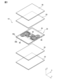
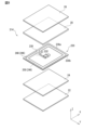
- FIG. 3 is an exploded perspective view of the RFIC module.
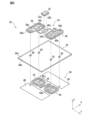
- FIG. 4 is an exploded perspective view of electronic components in the RFIC module.
- FIG. 5 is an equivalent circuit diagram of the wireless communication device.
- the RFIC module 14 is a device that performs wireless communication via antenna patterns 18A and 18B at a communication frequency in the 900 MHz band, that is, the UHF band, for example.
- the RFIC module 14 is an electronic component module with a multilayer structure including an electronic component 20.
- the RFIC module 14 includes an electronic component 20 and a hot melt adhesive layer 22 for attaching the electronic component 20 to the antenna member 12.
- the RFIC module 14 includes a bottom sheet 24 (second base material) interposed between the electronic component 20 and the hot melt adhesive layer 22, a top sheet 26, and a top sheet 26. and an adhesive sheet 28 for adhering the electronic component 20 to the electronic component 20.
- the electronic component 20 in the RFIC module 14 includes a base sheet 30 (first base material), an RFIC chip 32 mounted on one surface 30a of the base sheet 30, and an RFIC chip 32 mounted on one surface 30a of the base sheet 30. , and a conductive pattern 36 formed on the other surface 30b (first surface) of the base sheet 30 on the opposite side to the one surface 30a.
- the base sheet 30 in the electronic component 20 of the RFIC module 14 is a thin insulating sheet made of an insulating material such as polyimide or liquid crystal polymer.
- the RFIC chip 32 is an IC chip that is driven at a frequency in the UHF band (communication frequency), and has a structure in which various elements are built into a semiconductor substrate made of a semiconductor such as silicon. Further, the RFIC chip 32 includes a first input/output terminal 32a and a second input/output terminal 32b. Furthermore, as shown in FIG. 5, the RFIC chip 32 includes an internal capacitance (capacitance: self-capacitance that the RFIC chip itself has) C1.
- the conductor pattern 34 is a pattern made of a conductor material such as silver, copper, or aluminum.
- the conductor pattern 34 includes two spiral coil portions 38 and 40.
- a land portion 38a is provided at the outer peripheral end of the coil portion 38 in the conductor pattern 34, and is electrically connected to the first input/output terminal 32a of the RFIC chip 32 via, for example, solder (not shown). ing. Further, a land portion 38b for electrically connecting to the conductive pattern 36 is provided at the center side end of the coil portion 38. Further, the tip of a branch portion 38c branched from the portion of the coil portion 38 between the outer circumference side end (land portion 38a) and the center side end (land portion 38b) is also electrically connected to the conductor pattern 36. A land portion 38d is provided for this purpose.
- the coil section 38 functions as an inductance element having an inductance L1.
- a land portion 40a is provided at the outer peripheral end of the coil portion 40 in the conductor pattern 34, and is electrically connected to the second input/output terminal 32b of the RFIC chip 32 via, for example, solder (not shown). ing. Further, a land portion 40b for electrically connecting to the conductor pattern 36 is provided at the center side end of the coil portion 40. Further, the tip of a branch portion 40c branched from the portion of the coil portion 40 between the outer circumference side end (land portion 40a) and the center side end (land portion 40b) is also electrically connected to the conductor pattern 36. A land portion 40d is provided for this purpose.
- the coil section 40 functions as an inductance element having an inductance L2.
- the conductor pattern 36 is a pattern made of a conductor material such as silver, copper, or aluminum.
- the conductor pattern 36 includes two spiral coil portions 42 and 44 and two coupling electrodes 46 and 48.
- a land portion 42a is provided at the center side end of the coil portion 42 in the conductor pattern 36.
- the land portion 42 a is electrically connected to the land portion 38 b of the coil portion 38 in the conductor pattern 34 via an interlayer connection conductor 50 such as a through-hole conductor that penetrates the base sheet 30 .
- the coil section 42 functions as an inductance element having an inductance L3, as shown in FIG.
- a land portion 44a is provided at the center side end of the coil portion 44 in the conductor pattern 36.
- the land portion 44 a is connected to the land portion 40 b of the coil portion 40 in the conductor pattern 34 via an interlayer connection conductor 52 such as a through-hole conductor that penetrates the base sheet 30 .
- the coil section 44 functions as an inductance element having an inductance L4.
- the outer circumferential ends of the two coil parts 42 and 44 are electrically connected via a connecting part 54.
- the connecting portion 54 functions as an inductance element having an inductance L5.
- the coupling electrodes 46 and 48 in the conductor pattern 36 are electrodes for capacitive coupling with the coupling portions 18Ab and 18Bb of the antenna patterns 18A and 18B of the antenna member 12.
- the coupling electrodes 46 and 48 have a rectangular shape and are spaced apart.
- Coil portions 42, 44 and connection portion 54 are arranged between the coupling electrodes 46, 48.
- the coupling electrode 46 is electrically connected to the land portion 38d of the coil portion 38 in the conductor pattern 34 via an interlayer connection conductor 56 such as a through-hole conductor that penetrates the base sheet 30.
- the coupling electrode 48 is electrically connected to the land portion 40d of the coil portion 40 via an interlayer connection conductor 58.
- a matching circuit 60 is configured by the coil parts 38 and 40 in the conductor pattern 34, the coil parts 42 and 44 in the conductor pattern 36, the connection part 54, and the self-capacitance C1 of the RFIC chip 32.
- This matching circuit 60 matches the impedance between the RFIC chip 32 and the coupling electrodes 46 and 48 at a predetermined frequency (communication frequency).
- a hot melt adhesive layer 22 is provided on the other surface 30b of the base sheet 30 (ie, the surface on the antenna member 12 side) of the electronic component 20 of the RFIC module 14.
- the hot melt adhesive layer 22 has a bottom sheet 24 (second base material) between the other surface 30b of the base sheet 30 and the hot melt adhesive layer 22. It is provided on the other surface 30b of the base sheet 30 in an interposed state. Further, the hot melt adhesive layer 22 is provided on the base sheet 30 so as to cover the coupling electrodes 46 and 48.
- the hot melt adhesive constituting the hot melt adhesive layer 22 softens (partially melts) when heated from a hardened state, and hardens again when cooled in the softened state.
- the hot melt adhesive is, for example, an EVA-based thermoplastic resin that maintains a hardened state and does not deform at the temperature of the environment in which the wireless communication device 10 is used.
- the hot melt adhesive layer 22 in a hardened state has insulation properties.
- the hot melt adhesive layer 22 has a low melting temperature, for example 70 to 200 degrees, compared to other components of the RFIC module 14, such as the base sheet 30. When bonding, the hot melt adhesive layer 22 is heated to, for example, about 95 degrees to soften it.
- FIG. 6 is a cross-sectional view of a portion of the wireless communication device including the RFIC module just before attachment.
- the hot melt adhesive layer 22 is interposed between the RFIC module 14 and the antenna member 12 and adheres them to each other.
- the RFIC module 14 is mounted to the antenna member 12 with the coupling electrode 46 and the coupling portion 18Ab of the antenna pattern 18A facing each other, and the coupling electrode 48 and the coupling portion 18Bb of the antenna pattern 18B facing each other. Glued. Therefore, the coupling electrode 46 and the coupling portion 18Ab are capacitively coupled with the hot melt adhesive layer 22 and the bottom sheet 24 interposed therebetween (forming a capacitance C2 as shown in FIG. 5). Further, the coupling electrode 48 and the coupling portion 18Bb are capacitively coupled with each other with the hot melt adhesive layer 22 and the bottom sheet 24 interposed therebetween (forming a capacitance C3).
- the bottom sheet 24 (second base material) interposed between the base sheet 30 and the hot melt adhesive layer 22 is made of an insulating material such as epoxy resin, for example. Further, the bottom sheet 24 is provided on the other surface 30b of the base sheet 30 so as to cover the coupling electrodes 46 and 48. A hot melt adhesive layer 22 is provided on the surface of the bottom sheet 24 opposite to the surface facing the base sheet 30.
- the bottom sheet 24 is, for example, thermocompression bonded to the base sheet 30.
- the bottom sheet 24 protects the conductive pattern 36 including the coupling electrodes 46 and 48 on the other surface 30b of the base sheet 30. At the same time, the bottom sheet 24 is made up of variations in the distance between the coupling electrode 46 and the coupling part 18Ab of the antenna pattern 18A and the distance between the coupling electrode 48 and the coupling part 18Bb of the antenna pattern 18B, that is, variations in the capacitance between them. suppress.
- the hot melt adhesive layer 22 is present between the bonding electrode 46 and the bonding portion 18Ab, it is difficult to manage the distance between them. That is, when bonding the RFIC module 14 to the antenna member 12, it is necessary to control the thickness of the hot melt adhesive layer 22 so that the bonding electrode 46 and the bonding portion 18Ab are not short-circuited.
- the thickness of the bottom sheet 24 is constant, so that the coupling electrode 46 and the coupling portion 18Ab are not short-circuited. Thereby, it is possible to suppress variations in the distance between the coupling electrode 46 and the coupling portion 18Ab that would cause a short circuit.
- the top sheet 26 is a sheet-like member made of a resin material such as PET (polyethylene terephthalate), and is provided on one surface 30a of the base sheet 30.
- the top sheet 26 is adhered to the base sheet 30 via an adhesive sheet 28 made of, for example, epoxy resin.
- the top sheet 26 (and adhesive sheet 28) protects the IC chip 32 and conductor pattern 34 provided on one surface 30a of the base sheet 30.
- the adhesive sheet 28 is not limited to a thermosetting resin material.
- adhesives such as hot melt agents may also be used. This improves the adhesive strength between the top sheet 26 and the base sheet 30, and also improves the flexibility of the RFIC module when the hot melt agent is softer than the thermosetting resin.
- the antenna patterns 18A, 18B when the antenna patterns 18A, 18B receive a radio wave (signal) of a predetermined frequency (communication frequency) in the UHF band, the antenna pattern 18A, 18B transmits a signal to the RFIC chip 32 corresponding to the signal. Current flows. The RFIC chip 32 is driven by the supply of the current, and outputs a current (signal) corresponding to information stored in an internal storage section (not shown) to the antenna patterns 18A and 18B. Then, radio waves (signals) corresponding to the current are radiated from the antenna patterns 18A and 18B.
- the RFIC module 14 when bonding the RFIC module 14 to the antenna member 12, the RFIC module 14 is first placed on the antenna member 12.
- the RFIC module 14 is mounted on the antenna member 12 by a mounting device (not shown).
- the hot melt adhesive layer 22 is in a cured state and has no adhesive ability.
- the hot melt adhesive layer 22 is heated and softened.
- a heating device (not shown) that emits laser light LL (white arrow) is used to heat the hot melt adhesive layer 22.
- the RFIC module 14 is configured so that the hot melt adhesive layer 22 can be heated using the laser beam LL.
- the laser beam LL has a wavelength of, for example, about 900 nm, and is applied not to the hot melt adhesive layer 22 but to the coupling electrodes 46 and 48 covered with the hot melt adhesive layer 22. irradiated.
- the coupling electrodes 46 and 48 are heated by the laser beam LL, and are brought into a high temperature state throughout.
- Heat H black arrow
- Heat H moves from the bonding electrodes 46, 48 which are in a high temperature state to the hot melt adhesive layer 22 over the entirety thereof, and as a result, the entire hot melt adhesive layer 22 is heated and softened. That is, the coupling electrodes 46, 48 function as heat spreaders.
- the portion irradiated with the laser beam LL is excessively melted before the entire hot melt adhesive layer 22 is softened. For example, there is a possibility of liquefaction.
- the bonding electrodes 46 and 48 are preferably made of a material with high light absorption.
- coupling electrodes 46, 48 are preferably made of copper.
- an oxide film (copper oxide layer) having a high light absorption rate is formed on the surface thereof. As a result, the laser beam LL is absorbed by the coupling electrodes 46 and 48 without being reflected.
- thermal resistance refers to a numerical representation of the difficulty in transmitting heat, and the larger the value, the more difficult it is to transmit heat.
- the bottom sheet 24 is interposed between the bonding electrodes 46 and 48 and the hot melt adhesive layer 22. Therefore, the thermal resistance between the coupling electrodes 46, 48 and the bottom sheet 24 is smaller than the thermal resistance between the coupling electrodes 46, 48 and the base sheet 30.
- the hot melt adhesive layer 22 can be softened efficiently and in a short time.
- Conductive particles such as carbon particles and aluminum particles are dispersed therein.
- the base sheet 30 is made of polyimide
- the bottom sheet 24 is made of epoxy resin.
- the thermal conductivity of the former is 0.28 to 0.34 [W/m ⁇ K], and the latter is 0.3 [W/m ⁇ K]. Therefore, the thermal conductivity of the materials themselves of base sheet 30 and bottom sheet 24 are approximately the same. That is, the thermal resistance between the coupling electrodes 46, 48 and the base sheet 30 and the thermal resistance between the coupling electrodes 46, 48 and the bottom sheet 24 are substantially the same. Therefore, in the case of this embodiment, conductive particles are dispersed within the bottom sheet 24.
- the bottom sheet 24 may be made from a material with a high thermal conductivity compared to the thermal conductivity of the material of the base sheet 30. This also makes it possible to make the thermal resistance between the coupling electrodes 46, 48 and the bottom sheet 24 smaller than the thermal resistance between the coupling electrodes 46, 48 and the base sheet 30.
- the laser beam LL passes through the top sheet 26, adhesive sheet 28, and base sheet 30 and reaches the coupling electrodes 46 and 48.
- the top sheet 26, adhesive sheet 28, and base sheet 30 are made of a material through which light can pass.
- the base sheet 30 is preferably made of a material with a low light absorption compared to that of the bonding electrodes 46,48. Thereby, a higher amount of laser light LL can reach the coupling electrodes 46 and 48.
- the RFIC chip 32 is provided on one surface 30a of the base sheet 30, as shown in FIGS. 2 and 3. Further, the RFIC chip 32 is provided on one surface 30a of the base sheet 30 so as not to overlap the coupling electrodes 46 and 48 when viewed in plan (viewed in the Z-axis direction). Specifically, in the case of this embodiment, the coupling electrodes 46 and 48 are arranged at intervals in the longitudinal direction (X-axis direction). An RFIC chip 32 is located between the coupling electrodes 46, 48. This prevents the laser light LL from hitting the RFIC chip 32, and allows the laser light LL to reach the coupling electrodes 46 and 48 without being obstructed by the RFIC chip 32.
- the RFIC module 14 can be attached to the antenna member 12 including the antenna patterns 18A and 18B via the hot melt adhesive layer 22 in a short time.
- an insulating bottom sheet 24 is interposed between the electronic component 20 and the hot melt adhesive layer 22.
- the embodiments of the present disclosure are not limited to this.
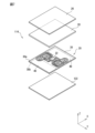
- FIG. 7 is an exploded perspective view of an RFIC module according to another embodiment of the present disclosure.
- a hot melt adhesive layer 122 is provided directly on the electronic component 20, similar to the bottom sheet 24 of the above-described embodiment, Coupling electrodes 46, 48 are covered. In this case, the thermal resistance between the bonding electrodes 46, 48 and the hot melt adhesive layer 122 is reduced compared to the thermal resistance between the bonding electrodes 46, 48 and the base sheet 30.
- the hot melt adhesive layer 22 for bonding the RFIC module 14 and the antenna member 12 is provided on the RFIC module 14.
- Hot melt adhesive layer 22 may be provided on antenna member 12 .
- the coupling electrodes 46 and 48 are heated by irradiation with the laser light LL. This is because the coupling electrodes 46, 48 are not exposed to the outside.
- the embodiments of the present disclosure are not limited to this. For example, a portion of the coupling electrodes 46, 48 may be exposed, a heat transfer member may be brought into contact with the exposed portion, and the heat transfer member may be heated.
- the coupling electrodes 46 and 48 of the electronic component 20 in the RFIC module 14 are capacitively coupled to the coupling portions 18Ab and 18Bb of the antenna patterns 18A and 18B of the antenna member 12. are doing.
- the coupling electrodes 46 and 48 are opposed to the coupling portions 18Ab and 18Bb with an interval in the thickness direction (Z-axis direction) of the wireless communication device 10. There is. That is, these are electrically coupled.
- embodiments of the present disclosure are not limited to electric field coupling.
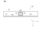
- FIG. 8 is a top view of a wireless communication device according to a different embodiment of the present disclosure.
- FIG. 9 is an exploded perspective view of an RFIC module in a wireless communication device according to a different embodiment.
- FIG. 10 is an exploded perspective view of electronic components in an RFIC module of a wireless communication device according to a different embodiment.
- the antenna member 212 includes an antenna pattern 218 that magnetically couples with the RFIC module 214.
- the antenna pattern 218 connects to a substantially “C”-shaped coupling portion 218a provided so as to surround the RFIC module 214, and extends from both ends of the coupling portion 218a to each other. It includes linear radiating portions 218b and 218c extending in opposite directions.
- the RFIC module 214 includes an electronic component 220, a bottom sheet 24 interposed between the electronic component 220 and the hot melt adhesive layer 22, a top sheet 26, and a top sheet 26 that is connected to the electronic component 220. and an adhesive sheet 28 for adhering to. Note that the bottom sheet 24 may be omitted.
- the electronic component 220 includes a base sheet 230, an RFIC chip 232 provided on the base sheet 230, and a coil conductor 246 (provided on the base sheet 230 and electrically connected to the RFIC chip 232). (coupling electrode).
- the coil conductor 246 includes a spiral conductor pattern 248 provided on one surface 230a of the base sheet 230, a spiral conductor pattern 250 provided on the other surface 230b, and a conductor pattern that penetrates the base sheet 230. 248, 250, and interlayer connection conductors 252, 254 such as through-hole conductors.
- the coil conductor 246 is provided on the base sheet 230 so as to surround the RFIC chip 232 when viewed in the thickness direction (Z-axis direction) of the wireless communication device 210.
- a current flows through the coupling portion 218a of the antenna pattern 218, thereby causing the coupling portion 218a to generate a magnetic field.
- the magnetic field causes current to flow in the coil conductor 246 of the electronic component 220 of the RFIC module 214.
- the RFIC chip 232 is driven by the supply of the current, and outputs a current to the coil conductor 246 that corresponds to information stored in an internal storage section (not shown).
- the coil conductor 246 generates a magnetic field corresponding to the output current, and the magnetic field causes a current to flow through the coupling portion 218a of the antenna pattern 218.
- the antenna pattern 218 emits radio waves corresponding to the current.
- the coil conductor 246 is heated by laser light irradiation.
- the coil conductor 246 heats and softens the hot melt adhesive layer 22, and as a result, the RFIC module 214 is bonded to the antenna member 212 via the hot melt adhesive layer 22.
- antenna patterns that can be magnetically coupled to the RFIC module 214.
- FIGS. 11 and 12 are top views of wireless communication devices according to modified examples of different embodiments.
- the antenna pattern 318 includes a substantially “C”-shaped coupling portion 318a provided so as to surround the RFIC module 214, and both ends of the coupling 318a. It includes meander-shaped radiating portions 318b and 318c extending in opposite directions from each other.
- an antenna pattern 418 includes linear radiating portions 418a and 418b that extend parallel to each other at intervals, and one end of these portions 418a and 418b extending in parallel. It includes a connecting portion 418c for connecting.
- the RFIC module 214 is surrounded by two radiating parts 418a, 418b and a connecting part 418c. Thereby, the RFIC module 214 is magnetically coupled to the antenna pattern 418.
- the electronic component module and members bonded via the hot melt adhesive layer 22 are the RFIC module 14 and the antenna member 12 in the wireless communication device, but in the embodiment of the present disclosure is not limited to this.
- a first aspect is an electronic component module that is attached to a member having a conductor pattern via a hot melt adhesive, the electronic component module including a first base material and a first base material on the member side. a coupling electrode provided on the surface of the first base material and electromagnetically coupled to the conductor pattern; and a second base material provided on the first surface of the first base material so as to cover the coupling electrode.
- a thermal resistance between the bonding electrode and the second base material is smaller than a thermal resistance between the bonding electrode and the first base material.
- a second aspect of the first aspect further includes a layer of the hot melt adhesive provided on a surface of the second base material opposite to a surface facing the first base material. It is an electronic component module.
- a third aspect is the electronic component module of the first or second aspect, in which conductive particles are dispersed in the second base material.
- a fourth aspect is one of the first to third aspects, wherein the second base material is made of a material having a higher thermal conductivity than the thermal conductivity of the material of the first base material. It is one of the electronic component modules.
- a fifth aspect is the electronic component module of the first aspect, wherein the second base material is the hot melt adhesive layer.
- the first base material is made of a material having a light absorption rate lower than that of the bonding electrode. It is a parts module.
- a seventh aspect further includes an IC chip provided on a second surface of the first base material opposite to the first surface and electrically connected to the bonding electrode, the IC chip is the electronic component module according to any one of the first to sixth aspects, wherein the electronic component module is provided on the second surface so as not to overlap the coupling electrode in a plan view of the first base material.
- An eighth aspect includes the electronic component module according to any one of the first to seventh aspects, and an antenna pattern that electromagnetically couples with a coupling electrode of the electronic component module, and the electronic component module is provided with a hot melt adhesive. and an antenna member attached through the antenna member.
- the present disclosure is applicable when an electronic component module including a coupling electrode and a member including a conductor pattern that capacitively or magnetically couples with the coupling electrode are attached via a hot melt adhesive.
Abstract
This electronic component module that is attached using a hot melt adhesive agent to a member provided with a conductor pattern comprises: a first base; a coupling electrode that is provided on a first surface of the first base for electromagnetic coupling with the conductor pattern; and a second base that is provided on the first surface of the first base to cover the coupling electrode. The thermal resistance between the coupling electrode and the second base is smaller than the thermal resistance between the coupling electrode and the first base.
Description
本開示は、電子部品モジュールおよびそれを備える無線通信デバイスに関する。
The present disclosure relates to an electronic component module and a wireless communication device including the same.
例えば、特許文献1には、アンテナパターン(導体パターン)が設けられたベースフィルム(部材)を実装位置に向かって搬送し、その実装位置でアンテナパターンにシール付きRFIC(Radio-Frequency Integrated Circuit)素子(電子部品モジュール)を貼り付けるRFIDタグ(無線通信デバイス)の製造方法が開示されている。テープに貼り付けられたシール付きRFIC素子をピックアップし、そのピックアップしたシール付きRFIC素子をアンテナパターンに貼り付ける(固定する)。
For example, in Patent Document 1, a base film (member) provided with an antenna pattern (conductor pattern) is transported toward a mounting position, and an RFIC (Radio-Frequency Integrated Circuit) element with a seal is attached to the antenna pattern at the mounting position. A method for manufacturing an RFID tag (wireless communication device) to which an electronic component module (electronic component module) is attached is disclosed. The RFIC element with the sticker attached to the tape is picked up, and the picked up RFIC element with the sticker is attached (fixed) to the antenna pattern.
しかしながら、特許文献1に記載された製造方法の場合、シール付きRFIC素子をテープから剥離しつつピックアップする必要があるため、そのピックアップに時間がかかる。また、RIFC素子の剥離に失敗する場合がある。
However, in the case of the manufacturing method described in Patent Document 1, since it is necessary to pick up the sealed RFIC element while peeling it from the tape, it takes time to pick it up. Furthermore, peeling of the RIFC element may fail.
なお、電子部品モジュールを部材に貼り付ける方法として、ホットメルト接着剤を用いることが考えられる。ホットメルト接着剤は、接着するタイミング以外では硬化状態にあるので、シールに比べて取り扱いやすい。しかし、接着時にホットメルト接着剤を加熱してその全体を軟化させる必要があり、その全体の軟化に時間を要する。
Note that a hot melt adhesive may be used as a method of attaching the electronic component module to the member. Hot melt adhesives are in a hardened state at times other than when they are bonded, so they are easier to handle than stickers. However, during bonding, it is necessary to heat the hot melt adhesive to soften the entirety, and it takes time to soften the entirety.
そこで、本開示は、電子部品モジュールを、ホットメルト接着剤を介して、導体パターンを備える部材に対して、短時間で貼り付けることを課題とする。
Therefore, an object of the present disclosure is to attach an electronic component module to a member provided with a conductor pattern via a hot melt adhesive in a short time.
上記技術的課題を解決するために、本開示の一態様によれば、
導体パターンを備える部材に対してホットメルト接着剤を介して貼り付けられる電子部品モジュールであって、
第1の基材と、
前記部材側の前記第1の基材の第1の表面に設けられ、前記導体パターンと電磁界結合する結合電極と、
前記結合電極を覆うように前記第1の基材の第1の表面に設けられた第2の基材と、を有し、
前記結合電極と前記第2の基材との間の熱抵抗が、前記結合電極と前記第1の基材との間の熱抵抗に比べて小さい、電子部品モジュールが提供される。 In order to solve the above technical problem, according to one aspect of the present disclosure,
An electronic component module that is attached to a member having a conductive pattern via a hot melt adhesive,
a first base material;
a coupling electrode provided on a first surface of the first base material on the member side and electromagnetically coupled to the conductor pattern;
a second base material provided on the first surface of the first base material so as to cover the bonding electrode,
An electronic component module is provided in which a thermal resistance between the bonding electrode and the second base material is smaller than a thermal resistance between the bonding electrode and the first base material.
また、本開示の別態様によれば、
前記電子部品モジュールと、
前記電子部品モジュールの結合電極と電磁界結合するアンテナパターンを備え、前記電子部品モジュールがホットメルト接着剤を介して貼り付けられるアンテナ部材と、を有する、無線通信デバイスが提供される。 Also, according to another aspect of the present disclosure,
the electronic component module;
A wireless communication device is provided, comprising an antenna member that includes an antenna pattern that electromagnetically couples with a coupling electrode of the electronic component module, and to which the electronic component module is attached via a hot melt adhesive.
本開示によれば、電子部品モジュールを、ホットメルト接着剤を介して、導体パターンを備える部材に対して、短時間で貼り付けることができる。
According to the present disclosure, an electronic component module can be attached to a member provided with a conductor pattern in a short time via a hot melt adhesive.
以下、本開示の実施の形態について、図面を参照しながら説明する。
Hereinafter, embodiments of the present disclosure will be described with reference to the drawings.
図1は、本開示の一実施の形態に係る無線通信デバイスの斜視図であって、図2は無線通信デバイスの上面図である。図中のX-Y-Z座標系は、本開示の理解を容易にするためのものであって、本開示を限定するものではない。X軸方向は無線通信デバイスの長手方向を示し、Y軸方向は幅方向を示し、Z軸方向は厚さ方向を示している。
FIG. 1 is a perspective view of a wireless communication device according to an embodiment of the present disclosure, and FIG. 2 is a top view of the wireless communication device. The XYZ coordinate system in the figures is for facilitating understanding of the present disclosure and is not intended to limit the present disclosure. The X-axis direction indicates the longitudinal direction of the wireless communication device, the Y-axis direction indicates the width direction, and the Z-axis direction indicates the thickness direction.
図1および図2に示すように、無線通信デバイス10は、ストリップ状であって、いわゆるRFID(Radio-Frequency IDentification)タグとして使用される。
As shown in FIGS. 1 and 2, the wireless communication device 10 has a strip shape and is used as a so-called RFID (Radio-Frequency IDentification) tag.
具体的には、図1および図2に示すように、無線通信デバイス10は、アンテナ部材12と、アンテナ部材12に設けられたRFIC(Radio-Frequency Integrated Circuit)モジュール14とを有する。
Specifically, as shown in FIGS. 1 and 2, the wireless communication device 10 includes an antenna member 12 and an RFIC (Radio-Frequency Integrated Circuit) module 14 provided in the antenna member 12.
無線通信デバイス10のアンテナ部材12は、ストリップ状(細長い矩形状)であって、アンテナ基材16と、アンテナ基材16の一方の表面16a(アンテナ部材12の第1の主面12a)に設けられたアンテナパターン18A、18Bとを備える。
The antenna member 12 of the wireless communication device 10 has a strip shape (elongated rectangular shape), and is provided on the antenna base material 16 and one surface 16a of the antenna base material 16 (first main surface 12a of the antenna member 12). antenna patterns 18A and 18B.
アンテナ基材16は、ポリイミド樹脂などの絶縁材料から作製された可撓性のシート状の部材である。図1および図2に示すように、アンテナ基材16はまた、アンテナ部材12の第1の主面12aおよび第2の主面12bとして機能する表面16a、16bを備える。アンテナ部材12の主要の構成要素であるアンテナ基材16が可撓性を備えるので、アンテナ部材12も可撓性を備えることができる。
The antenna base material 16 is a flexible sheet-like member made of an insulating material such as polyimide resin. As shown in FIGS. 1 and 2, antenna substrate 16 also includes surfaces 16a, 16b that function as first major surface 12a and second major surface 12b of antenna member 12. As shown in FIGS. Since the antenna base material 16, which is a main component of the antenna member 12, is flexible, the antenna member 12 can also be flexible.
アンテナパターン18A、18Bは、無線通信デバイス10が外部の通信装置(例えば、無線通信デバイス10がRFIDタグとして使用されている場合には、リーダ/ライター装置)と無線通信するためのアンテナとして使用される。本実施の形態の場合、アンテナパターン18A、18Bは、例えば、銀、銅、アルミニウムなどの金属箔から作製された導体パターンである。
The antenna patterns 18A and 18B are used as antennas for the wireless communication device 10 to wirelessly communicate with an external communication device (for example, a reader/writer device when the wireless communication device 10 is used as an RFID tag). Ru. In the case of this embodiment, the antenna patterns 18A and 18B are conductor patterns made of metal foil such as silver, copper, or aluminum, for example.
また、アンテナパターン18A、18Bは、電波を送受信するための放射部18Aa、18Baと、RFICモジュール14と電気的に接続するための結合部18Ab、18Bbとを含んでいる。
Furthermore, the antenna patterns 18A and 18B include radiating parts 18Aa and 18Ba for transmitting and receiving radio waves, and coupling parts 18Ab and 18Bb for electrically connecting to the RFIC module 14.
本実施の形態の場合、アンテナパターン18A、18Bの放射部18Aa、18Baは、ダイポールアンテナであって、ミアンダ状である。また、放射部18Aa、18Baそれぞれは、アンテナ基材16の長手方向(X軸方向)の中央部分に設けられた結合部18Ab、18Bbから該アンテナ基材16の両端に向かって延在する。
In the case of this embodiment, the radiating portions 18Aa and 18Ba of the antenna patterns 18A and 18B are dipole antennas and have a meander shape. Further, the radiating portions 18Aa and 18Ba each extend from coupling portions 18Ab and 18Bb provided at the central portion of the antenna base material 16 in the longitudinal direction (X-axis direction) toward both ends of the antenna base material 16.
アンテナパターン18A、18Bの結合部18Ab、18Bbは、詳細は後述するが、RFICモジュール14の結合電極と電気的に接続する。結合部18Ab、18Bbそれぞれは、矩形状のランドである。
The coupling portions 18Ab and 18Bb of the antenna patterns 18A and 18B are electrically connected to the coupling electrode of the RFIC module 14, as will be described in detail later. Each of the connecting portions 18Ab and 18Bb is a rectangular land.
図3は、RFICモジュールの分解斜視図である。また、図4は、RFICモジュールにおける電子部品の分解斜視図である。さらに、図5は、無線通信デバイスの等価回路図である。
FIG. 3 is an exploded perspective view of the RFIC module. Moreover, FIG. 4 is an exploded perspective view of electronic components in the RFIC module. Furthermore, FIG. 5 is an equivalent circuit diagram of the wireless communication device.
図3および図4に示すように、RFICモジュール14は、例えば900MHz帯、すなわちUHF帯の通信周波数でアンテナパターン18A、18Bを介して無線通信を行うデバイスである。
As shown in FIGS. 3 and 4, the RFIC module 14 is a device that performs wireless communication via antenna patterns 18A and 18B at a communication frequency in the 900 MHz band, that is, the UHF band, for example.
図3に示すように、本実施の形態の場合、RFICモジュール14は、電子部品20を含む多層構造の電子部品モジュールである。具体的には、RFICモジュール14は、電子部品20と、電子部品20をアンテナ部材12に貼り付けるためのホットメルト接着剤層22とを含んでいる。さらに、本実施の形態の場合、RFICモジュール14は、電子部品20とホットメルト接着剤層22との間に介在するボトムシート24(第2の基材)と、トップシート26と、トップシート26を電子部品20に接着するための接着シート28とを含んでいる。
As shown in FIG. 3, in this embodiment, the RFIC module 14 is an electronic component module with a multilayer structure including an electronic component 20. Specifically, the RFIC module 14 includes an electronic component 20 and a hot melt adhesive layer 22 for attaching the electronic component 20 to the antenna member 12. Furthermore, in the case of the present embodiment, the RFIC module 14 includes a bottom sheet 24 (second base material) interposed between the electronic component 20 and the hot melt adhesive layer 22, a top sheet 26, and a top sheet 26. and an adhesive sheet 28 for adhering the electronic component 20 to the electronic component 20.
図4に示すように、RFICモジュール14における電子部品20は、ベースシート30(第1の基材)と、ベースシート30の一方の表面30aに実装されたRFICチップ32と、ベースシート30の一方の表面30aに形成された導体パターン34と、一方の表面30aに対して反対側のベースシート30の他方の表面30b(第1の表面)に形成された導体パターン36とを含んでいる。
As shown in FIG. 4, the electronic component 20 in the RFIC module 14 includes a base sheet 30 (first base material), an RFIC chip 32 mounted on one surface 30a of the base sheet 30, and an RFIC chip 32 mounted on one surface 30a of the base sheet 30. , and a conductive pattern 36 formed on the other surface 30b (first surface) of the base sheet 30 on the opposite side to the one surface 30a.
RFICモジュール14の電子部品20におけるベースシート30は、薄板状の絶縁シートであって、例えば、ポリイミドや液晶ポリマなどの絶縁材料から作製されている。
The base sheet 30 in the electronic component 20 of the RFIC module 14 is a thin insulating sheet made of an insulating material such as polyimide or liquid crystal polymer.
RFICチップ32は、UHF帯の周波数(通信周波数)で駆動するICチップであって、シリコン等の半導体を素材とする半導体基板に各種の素子を内蔵した構造を有する。また、RFICチップ32は、第1の入出力端子32aと第2の入出力端子32bとを備える。さらに、図5に示すように、RFICチップ32は、内部容量(キャパシタンス:RFICチップ自身が持つ自己容量)C1を備える。
The RFIC chip 32 is an IC chip that is driven at a frequency in the UHF band (communication frequency), and has a structure in which various elements are built into a semiconductor substrate made of a semiconductor such as silicon. Further, the RFIC chip 32 includes a first input/output terminal 32a and a second input/output terminal 32b. Furthermore, as shown in FIG. 5, the RFIC chip 32 includes an internal capacitance (capacitance: self-capacitance that the RFIC chip itself has) C1.
導体パターン34は、銀、銅、アルミニウムなどの導体材料から作製されたパターンである。導体パターン34には、2つのスパイラル状のコイル部38、40が含まれている。
The conductor pattern 34 is a pattern made of a conductor material such as silver, copper, or aluminum. The conductor pattern 34 includes two spiral coil portions 38 and 40.
導体パターン34におけるコイル部38の外周側端には、RFICチップ32の第1の入出力端子32aに対して、例えばはんだ(図示せず)を介して電気的に接続するランド部38aが設けられている。また、コイル部38の中心側端には、導体パターン36と電気的に接続するためのランド部38bが設けられている。また、外周側端(ランド部38a)と中心側端(ランド部38b)との間のコイル部38の部分から分枝した分枝部38cの先端にも、導体パターン36と電気的に接続するためのランド部38dが設けられている。
A land portion 38a is provided at the outer peripheral end of the coil portion 38 in the conductor pattern 34, and is electrically connected to the first input/output terminal 32a of the RFIC chip 32 via, for example, solder (not shown). ing. Further, a land portion 38b for electrically connecting to the conductive pattern 36 is provided at the center side end of the coil portion 38. Further, the tip of a branch portion 38c branched from the portion of the coil portion 38 between the outer circumference side end (land portion 38a) and the center side end (land portion 38b) is also electrically connected to the conductor pattern 36. A land portion 38d is provided for this purpose.
また、コイル部38は、図5に示すように、インダクタンスL1を持つインダクタンス素子として機能する。
Further, as shown in FIG. 5, the coil section 38 functions as an inductance element having an inductance L1.
導体パターン34におけるコイル部40の外周側端には、RFICチップ32の第2の入出力端子32bに対して、例えばはんだ(図示せず)を介して電気的に接続するランド部40aが設けられている。また、コイル部40の中心側端には、導体パターン36と電気的に接続するためのランド部40bが設けられている。また、外周側端(ランド部40a)と中心側端(ランド部40b)との間のコイル部40の部分から分枝した分枝部40cの先端にも、導体パターン36と電気的に接続するためのランド部40dが設けられている。
A land portion 40a is provided at the outer peripheral end of the coil portion 40 in the conductor pattern 34, and is electrically connected to the second input/output terminal 32b of the RFIC chip 32 via, for example, solder (not shown). ing. Further, a land portion 40b for electrically connecting to the conductor pattern 36 is provided at the center side end of the coil portion 40. Further, the tip of a branch portion 40c branched from the portion of the coil portion 40 between the outer circumference side end (land portion 40a) and the center side end (land portion 40b) is also electrically connected to the conductor pattern 36. A land portion 40d is provided for this purpose.
また、コイル部40は、図5に示すように、インダクタンスL2を持つインダクタンス素子として機能する。
Further, as shown in FIG. 5, the coil section 40 functions as an inductance element having an inductance L2.
導体パターン36は、銀、銅、アルミニウムなどの導体材料から作製されたパターンである。導体パターン36には、2つのスパイラル状のコイル部42、44と、2つの結合電極46、48とが含まれている。
The conductor pattern 36 is a pattern made of a conductor material such as silver, copper, or aluminum. The conductor pattern 36 includes two spiral coil portions 42 and 44 and two coupling electrodes 46 and 48.
導体パターン36におけるコイル部42の中心側端には、ランド部42aが設けられている。ランド部42aは、ベースシート30を貫通するスルーホール導体などの層間接続導体50を介して、導体パターン34におけるコイル部38のランド部38bに電気的に接続している。
A land portion 42a is provided at the center side end of the coil portion 42 in the conductor pattern 36. The land portion 42 a is electrically connected to the land portion 38 b of the coil portion 38 in the conductor pattern 34 via an interlayer connection conductor 50 such as a through-hole conductor that penetrates the base sheet 30 .
また、コイル部42は、図5に示すように、インダクタンスL3を持つインダクタンス素子として機能する。
Furthermore, the coil section 42 functions as an inductance element having an inductance L3, as shown in FIG.
導体パターン36におけるコイル部44の中心側端には、ランド部44aが設けられている。ランド部44aは、ベースシート30を貫通するスルーホール導体などの層間接続導体52を介して、導体パターン34におけるコイル部40のランド部40bに接続している。
A land portion 44a is provided at the center side end of the coil portion 44 in the conductor pattern 36. The land portion 44 a is connected to the land portion 40 b of the coil portion 40 in the conductor pattern 34 via an interlayer connection conductor 52 such as a through-hole conductor that penetrates the base sheet 30 .
また、コイル部44は、図5に示すように、インダクタンスL4を持つインダクタンス素子として機能する。
Further, as shown in FIG. 5, the coil section 44 functions as an inductance element having an inductance L4.
2つのコイル部42、44それぞれの外周側端は、接続部54を介して、電気的に接続されている。接続部54は、インダクタンスL5を持つインダクタンス素子として機能する。
The outer circumferential ends of the two coil parts 42 and 44 are electrically connected via a connecting part 54. The connecting portion 54 functions as an inductance element having an inductance L5.
導体パターン36における結合電極46、48は、アンテナ部材12のアンテナパターン18A、18Bの結合部18Ab、18Bbと容量結合するための電極である。本実施の形態の場合、結合電極46、48は、矩形状であって、間隔をあけて配置されている。その結合電極46、48の間に、コイル部42、44、および接続部54が配置されている。
The coupling electrodes 46 and 48 in the conductor pattern 36 are electrodes for capacitive coupling with the coupling portions 18Ab and 18Bb of the antenna patterns 18A and 18B of the antenna member 12. In this embodiment, the coupling electrodes 46 and 48 have a rectangular shape and are spaced apart. Coil portions 42, 44 and connection portion 54 are arranged between the coupling electrodes 46, 48.
結合電極46は、ベースシート30を貫通するスルーホール導体などの層間接続導体56を介して、導体パターン34におけるコイル部38のランド部38dに電気的に接続している。結合電極48は、層間接続導体58を介して、コイル部40のランド部40dに電気的に接続している。
The coupling electrode 46 is electrically connected to the land portion 38d of the coil portion 38 in the conductor pattern 34 via an interlayer connection conductor 56 such as a through-hole conductor that penetrates the base sheet 30. The coupling electrode 48 is electrically connected to the land portion 40d of the coil portion 40 via an interlayer connection conductor 58.
図5に示すように、導体パターン34におけるコイル部38、40、導体パターン36におけるコイル部42、44と接続部54、およびRFICチップ32の自己容量C1により、整合回路60が構成されている。この整合回路60により、RFICチップ32と結合電極46、48との間のインピーダンスが所定の周波数(通信周波数)で整合されている。
As shown in FIG. 5, a matching circuit 60 is configured by the coil parts 38 and 40 in the conductor pattern 34, the coil parts 42 and 44 in the conductor pattern 36, the connection part 54, and the self-capacitance C1 of the RFIC chip 32. This matching circuit 60 matches the impedance between the RFIC chip 32 and the coupling electrodes 46 and 48 at a predetermined frequency (communication frequency).
図3に戻り、RFICモジュール14の電子部品20におけるベースシート30の他方の表面30b(すなわちアンテナ部材12側の表面)には、ホットメルト接着剤層22が設けられている。具体的には、本実施の形態の場合、ホットメルト接着剤層22は、ベースシート30の他方の表面30bとホットメルト接着剤層22との間にボトムシート24(第2の基材)が介在した状態で、ベースシート30の他方の表面30bに設けられている。また、ホットメルト接着剤層22は、結合電極46、48を覆うように、ベースシート30に設けられている。
Returning to FIG. 3, a hot melt adhesive layer 22 is provided on the other surface 30b of the base sheet 30 (ie, the surface on the antenna member 12 side) of the electronic component 20 of the RFIC module 14. Specifically, in the case of the present embodiment, the hot melt adhesive layer 22 has a bottom sheet 24 (second base material) between the other surface 30b of the base sheet 30 and the hot melt adhesive layer 22. It is provided on the other surface 30b of the base sheet 30 in an interposed state. Further, the hot melt adhesive layer 22 is provided on the base sheet 30 so as to cover the coupling electrodes 46 and 48.
ホットメルト接着剤層22を構成するホットメルト接着剤は、硬化状態から加熱されると軟化(部分的に溶融)し、軟化状態で冷却されると再び硬化する。本実施の形態の場合、ホットメルト接着剤は、無線通信デバイス10の使用環境の温度では硬化状態を維持して変形しない、例えばEVA系の熱可塑性樹脂である。また、本実施の形態の場合、硬化状態のホットメルト接着剤層22は、絶縁性を備える。さらに本実施の形態の場合、ホットメルト接着剤層22は、ベースシート30などのRFICモジュール14の他の構成要素に比べて低い溶融温度、例えば70~200度の溶融温度を備える。接着するとき、ホットメルト接着剤層22は、例えば約95度に加熱されて軟化される。
The hot melt adhesive constituting the hot melt adhesive layer 22 softens (partially melts) when heated from a hardened state, and hardens again when cooled in the softened state. In the case of this embodiment, the hot melt adhesive is, for example, an EVA-based thermoplastic resin that maintains a hardened state and does not deform at the temperature of the environment in which the wireless communication device 10 is used. Moreover, in the case of this embodiment, the hot melt adhesive layer 22 in a hardened state has insulation properties. Further, in this embodiment, the hot melt adhesive layer 22 has a low melting temperature, for example 70 to 200 degrees, compared to other components of the RFIC module 14, such as the base sheet 30. When bonding, the hot melt adhesive layer 22 is heated to, for example, about 95 degrees to soften it.
図6は、貼り付け直前のRFICモジュールを含む無線通信デバイスの一部分の断面図である。
FIG. 6 is a cross-sectional view of a portion of the wireless communication device including the RFIC module just before attachment.
図6に示すように、ホットメルト接着剤層22は、RFICモジュール14とアンテナ部材12との間に介在し、これらを互いに接着する。具体的には、RFICモジュール14は、結合電極46とアンテナパターン18Aの結合部18Abとが対向しつつ結合電極48とアンテナパターン18Bの結合部18Bbとが対向した状態で、アンテナ部材12に対して接着される。したがって、結合電極46と結合部18Abは、それらの間にホットメルト接着剤層22とボトムシート24とが介在した状態で容量結合する(図5に示すようにキャパシタンスC2を形成する)。また、結合電極48と結合部18Bbは、それらの間にホットメルト接着剤層22とボトムシート24とが介在した状態で容量結合する(キャパシタンスC3を形成する)。
As shown in FIG. 6, the hot melt adhesive layer 22 is interposed between the RFIC module 14 and the antenna member 12 and adheres them to each other. Specifically, the RFIC module 14 is mounted to the antenna member 12 with the coupling electrode 46 and the coupling portion 18Ab of the antenna pattern 18A facing each other, and the coupling electrode 48 and the coupling portion 18Bb of the antenna pattern 18B facing each other. Glued. Therefore, the coupling electrode 46 and the coupling portion 18Ab are capacitively coupled with the hot melt adhesive layer 22 and the bottom sheet 24 interposed therebetween (forming a capacitance C2 as shown in FIG. 5). Further, the coupling electrode 48 and the coupling portion 18Bb are capacitively coupled with each other with the hot melt adhesive layer 22 and the bottom sheet 24 interposed therebetween (forming a capacitance C3).
ベースシート30とホットメルト接着剤層22との間に介在するボトムシート24(第2の基材)は、例えば、エポキシ樹脂などの絶縁材料から作製されている。また、ボトムシート24は、結合電極46、48を覆うように、ベースシート30の他方の表面30bに設けられている。そして、ベースシート30に対向する表面とは反対側のボトムシート24の表面に、ホットメルト接着剤層22が設けられている。ボトムシート24は、例えば、ベースシート30に熱圧着されている。
The bottom sheet 24 (second base material) interposed between the base sheet 30 and the hot melt adhesive layer 22 is made of an insulating material such as epoxy resin, for example. Further, the bottom sheet 24 is provided on the other surface 30b of the base sheet 30 so as to cover the coupling electrodes 46 and 48. A hot melt adhesive layer 22 is provided on the surface of the bottom sheet 24 opposite to the surface facing the base sheet 30. The bottom sheet 24 is, for example, thermocompression bonded to the base sheet 30.
ボトムシート24は、ベースシート30の他方の表面30b上の結合電極46、48を含む導体パターン36を保護する。それととともに、ボトムシート24は、結合電極46とアンテナパターン18Aの結合部18Abの間の距離および結合電極48とアンテナパターン18Bの結合部18Bbの間の距離のバラツキ、すなわちこれらの間の容量のバラツキを抑制する。
The bottom sheet 24 protects the conductive pattern 36 including the coupling electrodes 46 and 48 on the other surface 30b of the base sheet 30. At the same time, the bottom sheet 24 is made up of variations in the distance between the coupling electrode 46 and the coupling part 18Ab of the antenna pattern 18A and the distance between the coupling electrode 48 and the coupling part 18Bb of the antenna pattern 18B, that is, variations in the capacitance between them. suppress.
例えば、結合電極46と結合部18Abとの間にホットメルト接着剤層22のみ存在する場合、これらの間の距離の管理が難しい。すなわち、RFICモジュール14をアンテナ部材12に接着するときに、結合電極46と結合部18Abとが短絡しないようにホットメルト接着剤層22の厚さを管理する必要がある。これに対して、結合電極46と結合部18Abとの間にボトムシート24が存在する場合、ボトムシート24の厚さが一定であるので、結合電極46と結合部18Abとが短絡しない。これにより、短絡が生じるような結合電極46と結合部18Abとの間の距離のバラツキを抑制することができる。
For example, if only the hot melt adhesive layer 22 is present between the bonding electrode 46 and the bonding portion 18Ab, it is difficult to manage the distance between them. That is, when bonding the RFIC module 14 to the antenna member 12, it is necessary to control the thickness of the hot melt adhesive layer 22 so that the bonding electrode 46 and the bonding portion 18Ab are not short-circuited. On the other hand, when the bottom sheet 24 is present between the coupling electrode 46 and the coupling portion 18Ab, the thickness of the bottom sheet 24 is constant, so that the coupling electrode 46 and the coupling portion 18Ab are not short-circuited. Thereby, it is possible to suppress variations in the distance between the coupling electrode 46 and the coupling portion 18Ab that would cause a short circuit.
トップシート26は、例えば、PET(ポリエチレンテレフタレート)などの樹脂材料から作製されたシート状の部材であって、ベースシート30の一方の表面30aに設けられている。トップシート26は、例えば、エポキシ樹脂から作製された接着シート28を介してベースシート30に接着されている。これにより、トップシート26(および接着シート28)は、ベースシート30の一方の表面30aに設けられたICチップ32および導体パターン34を保護する。ここで、接着シート28は熱硬化性樹脂材料に限られない。熱硬化性樹脂材料以外にもホットメルト剤のような接着剤を用いてもよい。これによりトップシート26とベースシート30の接着強度を向上させ、また、熱硬化性樹脂よりホットメルト剤が柔らかい場合には、RFICモジュールのフレキシブル性を向上することができる。
The top sheet 26 is a sheet-like member made of a resin material such as PET (polyethylene terephthalate), and is provided on one surface 30a of the base sheet 30. The top sheet 26 is adhered to the base sheet 30 via an adhesive sheet 28 made of, for example, epoxy resin. Thereby, the top sheet 26 (and adhesive sheet 28) protects the IC chip 32 and conductor pattern 34 provided on one surface 30a of the base sheet 30. Here, the adhesive sheet 28 is not limited to a thermosetting resin material. In addition to thermosetting resin materials, adhesives such as hot melt agents may also be used. This improves the adhesive strength between the top sheet 26 and the base sheet 30, and also improves the flexibility of the RFIC module when the hot melt agent is softer than the thermosetting resin.
このような無線通信デバイス10によれば、アンテナパターン18A、18BがUHF帯の所定の周波数(通信周波数)の電波(信号)を受信すると、アンテナパターン18A、18BからRFICチップ32に信号に対応する電流が流れる。その電流の供給を受けてRFICチップ32は駆動し、その内部の記憶部(図示せず)に記憶されている情報に対応する電流(信号)をアンテナパターン18A、18Bに出力する。そして、その電流に対応する電波(信号)がアンテナパターン18A、18Bから放射される。
According to such a wireless communication device 10, when the antenna patterns 18A, 18B receive a radio wave (signal) of a predetermined frequency (communication frequency) in the UHF band, the antenna pattern 18A, 18B transmits a signal to the RFIC chip 32 corresponding to the signal. Current flows. The RFIC chip 32 is driven by the supply of the current, and outputs a current (signal) corresponding to information stored in an internal storage section (not shown) to the antenna patterns 18A and 18B. Then, radio waves (signals) corresponding to the current are radiated from the antenna patterns 18A and 18B.
ここまでは、本実施の形態に係る無線通信デバイス10の構成について説明してきた。ここからは、RFICモジュール14をそのホットメルト接着剤層22を介してアンテナ部材12に接着する方法について説明する。
Up to this point, the configuration of the wireless communication device 10 according to the present embodiment has been described. From here on, a method for bonding the RFIC module 14 to the antenna member 12 via the hot melt adhesive layer 22 will be described.
図6に示すように、RFICモジュール14をアンテナ部材12に接着するとき、まず、RFICモジュール14がアンテナ部材12上に載置される。例えば、RFICモジュール14は、実装装置(図示せず)によってアンテナ部材12上に載置される。RFICモジュール14がアンテナ部材12上に載置されるとき、ホットメルト接着剤層22は、硬化状態であって、接着能力を持たない。
As shown in FIG. 6, when bonding the RFIC module 14 to the antenna member 12, the RFIC module 14 is first placed on the antenna member 12. For example, the RFIC module 14 is mounted on the antenna member 12 by a mounting device (not shown). When the RFIC module 14 is placed on the antenna member 12, the hot melt adhesive layer 22 is in a cured state and has no adhesive ability.
RFICモジュール14がアンテナ部材12上に載置されると、ホットメルト接着剤層22が加熱されて軟化される。本実施の形態の場合、ホットメルト接着剤層22を加熱するために、レーザ光LL(白抜き矢印)を出射する加熱装置(図示せず)が使用される。レーザ光LLを用いてホットメルト接着剤層22を加熱することができるように、RFICモジュール14は構成されている。
When the RFIC module 14 is placed on the antenna member 12, the hot melt adhesive layer 22 is heated and softened. In the case of this embodiment, a heating device (not shown) that emits laser light LL (white arrow) is used to heat the hot melt adhesive layer 22. The RFIC module 14 is configured so that the hot melt adhesive layer 22 can be heated using the laser beam LL.
具体的には、図6に示すように、レーザ光LLは、例えば約900nmの波長を備え、ホットメルト接着剤層22ではなく、ホットメルト接着剤層22に覆われた結合電極46、48に照射される。結合電極46、48は、レーザ光LLによって加熱され、その全体にわたって高温状態になる。その全体にわたって高温状態の結合電極46、48からホットメルト接着剤層22に熱H(黒塗り矢印)が移動し、その結果としてホットメルト接着剤層22全体にわたって加熱されて軟化する。すなわち、結合電極46、48は、ヒートスプレッダとして機能する。なお、これと異なり、レーザ光LLをホットメルト接着剤層22に直接的に照射した場合、ホットメルト接着剤層22が全体にわたって軟化する前に、レーザ光LLが照射された部分が過剰に溶融する、例えば液状化する可能性がある。
Specifically, as shown in FIG. 6, the laser beam LL has a wavelength of, for example, about 900 nm, and is applied not to the hot melt adhesive layer 22 but to the coupling electrodes 46 and 48 covered with the hot melt adhesive layer 22. irradiated. The coupling electrodes 46 and 48 are heated by the laser beam LL, and are brought into a high temperature state throughout. Heat H (black arrow) moves from the bonding electrodes 46, 48 which are in a high temperature state to the hot melt adhesive layer 22 over the entirety thereof, and as a result, the entire hot melt adhesive layer 22 is heated and softened. That is, the coupling electrodes 46, 48 function as heat spreaders. Note that, unlike this, when the hot melt adhesive layer 22 is directly irradiated with the laser beam LL, the portion irradiated with the laser beam LL is excessively melted before the entire hot melt adhesive layer 22 is softened. For example, there is a possibility of liquefaction.
このようにレーザ光LLを用いてヒートスプレッダとして機能する結合電極46、48を加熱する場合、結合電極46、48は、光吸収率が高い材料で作製されるのが好ましい。そのために、結合電極46、48は、銅から作製されるのが好ましい。結合電極46、48が銅から作製される場合、その表面に光吸収率が高い酸化膜(酸化銅の層)が形成される。その結果、レーザ光LLが反射されることなく、結合電極46、48に吸収される。
When heating the bonding electrodes 46 and 48 functioning as heat spreaders using the laser beam LL in this manner, the bonding electrodes 46 and 48 are preferably made of a material with high light absorption. To that end, coupling electrodes 46, 48 are preferably made of copper. When the coupling electrodes 46 and 48 are made of copper, an oxide film (copper oxide layer) having a high light absorption rate is formed on the surface thereof. As a result, the laser beam LL is absorbed by the coupling electrodes 46 and 48 without being reflected.
このような結合電極46、48を介するホットメルト接着剤層22の加熱を効率的に実行するために、結合電極46、48とホットメルト接着剤層22との間の熱抵抗が、結合電極46、48とベースシート30との間の熱抵抗に比べて小さくされている。なお、本明細書で言う「熱抵抗」は、熱の伝わり難さを数値化したものを言い、値が大きいほど熱が伝わり難い。
In order to efficiently heat the hot melt adhesive layer 22 through such bonding electrodes 46 , 48 , the thermal resistance between the bonding electrodes 46 , 48 and the hot melt adhesive layer 22 is such that the bonding electrode 46 , 48 and the base sheet 30. Note that the term "thermal resistance" as used herein refers to a numerical representation of the difficulty in transmitting heat, and the larger the value, the more difficult it is to transmit heat.
なお、本実施の形態の場合には、結合電極46、48とホットメルト接着剤層22との間にボトムシート24が介在する。そのため、結合電極46、48とボトムシート24との間の熱抵抗が、結合電極46、48とベースシート30との間の熱抵抗に比べて小さくされている。
Note that in the case of this embodiment, the bottom sheet 24 is interposed between the bonding electrodes 46 and 48 and the hot melt adhesive layer 22. Therefore, the thermal resistance between the coupling electrodes 46, 48 and the bottom sheet 24 is smaller than the thermal resistance between the coupling electrodes 46, 48 and the base sheet 30.
この熱抵抗の違いにより、レーザ光LLによって加熱された結合電極46、48で発生した熱の多くが、ボトムシート24を介して、ホットメルト接着剤層22に移動する。これにより、効率的に、短時間でホットメルト接着剤層22を軟化させることができる。
Due to this difference in thermal resistance, most of the heat generated in the bonding electrodes 46 and 48 heated by the laser beam LL moves to the hot melt adhesive layer 22 via the bottom sheet 24. Thereby, the hot melt adhesive layer 22 can be softened efficiently and in a short time.
結合電極46、48とボトムシート24との間の熱抵抗を結合電極46、48とベースシート30との間の熱抵抗に比べて小さくするために、本実施の形態の場合、ボトムシート24内に、カーボン粒子、アルミ粒子などの導電粒子が分散されている。
In this embodiment, in order to make the thermal resistance between the bonding electrodes 46, 48 and the bottom sheet 24 smaller than the thermal resistance between the bonding electrodes 46, 48 and the base sheet 30, Conductive particles such as carbon particles and aluminum particles are dispersed therein.
本実施の形態の場合、ベースシート30はポリイミドから作製され、ボトムシート24はエポキシ樹脂から作製されている。熱伝導率は、前者が0.28~0.34[W/m・K]であって、後者が0.3[W/m・K]である。したがって、ベースシート30およびボトムシート24の材料自体の熱伝導率はほぼ同じである。すなわち、結合電極46、48とベースシート30との間の熱抵抗と結合電極46、48とボトムシート24との間の熱抵抗が実質的に同じである。そこで、本実施の形態の場合、ボトムシート24内に、導電粒子が分散されている。
In the case of this embodiment, the base sheet 30 is made of polyimide, and the bottom sheet 24 is made of epoxy resin. The thermal conductivity of the former is 0.28 to 0.34 [W/m·K], and the latter is 0.3 [W/m·K]. Therefore, the thermal conductivity of the materials themselves of base sheet 30 and bottom sheet 24 are approximately the same. That is, the thermal resistance between the coupling electrodes 46, 48 and the base sheet 30 and the thermal resistance between the coupling electrodes 46, 48 and the bottom sheet 24 are substantially the same. Therefore, in the case of this embodiment, conductive particles are dispersed within the bottom sheet 24.
熱伝導率が高い導電粒子がボトムシート24内に分散されると、結合電極46、48からボトムシート24内に熱が移動しやすくなる。その一方、ベースシート30には導電粒子を分散させない。これにより、ボトムシート24とベースシート30の材料の熱伝導率が実質的に同じであっても、結合電極46、48とボトムシート24との間の熱抵抗を、結合電極46、48とベースシートとの間の熱抵抗に比べて小さくすることができる。したがって、結合電極46、48で発生した熱Hの多くは、ベースシート30ではなく、ボトムシート24に移動することができる。
When conductive particles with high thermal conductivity are dispersed within the bottom sheet 24, heat is easily transferred from the bonding electrodes 46, 48 into the bottom sheet 24. On the other hand, conductive particles are not dispersed in the base sheet 30. This reduces the thermal resistance between the bonding electrodes 46, 48 and the bottom sheet 24 even though the materials of the bottom sheet 24 and the base sheet 30 have substantially the same thermal conductivity. The thermal resistance can be made smaller than that between the sheet and the sheet. Therefore, much of the heat H generated at the coupling electrodes 46, 48 can be transferred to the bottom sheet 24 instead of the base sheet 30.
導電粒子をボトムシート24内に分散させることに加えてまたは代わって、ボトムシート24を、ベースシート30の材料の熱伝導率に比べて高い熱伝導率を備える材料から作製してもよい。これによっても、結合電極46、48とボトムシート24との間の熱抵抗を結合電極46、48とベースシート30との間の熱抵抗に比べて小さくすることができる。
In addition to or instead of having conductive particles dispersed within the bottom sheet 24, the bottom sheet 24 may be made from a material with a high thermal conductivity compared to the thermal conductivity of the material of the base sheet 30. This also makes it possible to make the thermal resistance between the coupling electrodes 46, 48 and the bottom sheet 24 smaller than the thermal resistance between the coupling electrodes 46, 48 and the base sheet 30.
また、本実施の形態の場合、図6に示すように、レーザ光LLは、トップシート26、接着シート28、およびベースシート30を透過して結合電極46、48に到達する。そのために、トップシート26、接着シート28、およびベースシート30は、光が透過可能な材料から作製されている。特に、ベースシート30は、結合電極46,48の光吸収率に比べて低い光吸収率を備える材料から作製されるのが好ましい。これにより、結合電極46、48に、より高い光量のレーザ光LLが到達することができる。
Further, in the case of this embodiment, as shown in FIG. 6, the laser beam LL passes through the top sheet 26, adhesive sheet 28, and base sheet 30 and reaches the coupling electrodes 46 and 48. To this end, the top sheet 26, adhesive sheet 28, and base sheet 30 are made of a material through which light can pass. In particular, the base sheet 30 is preferably made of a material with a low light absorption compared to that of the bonding electrodes 46,48. Thereby, a higher amount of laser light LL can reach the coupling electrodes 46 and 48.
さらに、本実施の形態の場合、図2および図3に示すように、RFICチップ32は、ベースシート30の一方の表面30aに設けられている。また、RFICチップ32は、ベースシート30の平面視(Z軸方向視)で、結合電極46、48にオーバーラップしないように、一方の表面30aに設けられている。具体的には、本実施の形態の場合、結合電極46、48は、長手方向(X軸方向)に間隔をあけて並んでいる。その結合電極46、48の間に、RFICチップ32が位置する。これにより、RFICチップ32にレーザ光LLが当たることが抑制されるともに、レーザ光LLがRFICチップ32に邪魔されることなく結合電極46、48に到達することができる。
Furthermore, in the case of this embodiment, the RFIC chip 32 is provided on one surface 30a of the base sheet 30, as shown in FIGS. 2 and 3. Further, the RFIC chip 32 is provided on one surface 30a of the base sheet 30 so as not to overlap the coupling electrodes 46 and 48 when viewed in plan (viewed in the Z-axis direction). Specifically, in the case of this embodiment, the coupling electrodes 46 and 48 are arranged at intervals in the longitudinal direction (X-axis direction). An RFIC chip 32 is located between the coupling electrodes 46, 48. This prevents the laser light LL from hitting the RFIC chip 32, and allows the laser light LL to reach the coupling electrodes 46 and 48 without being obstructed by the RFIC chip 32.
以上、本実施の形態によれば、RFICモジュール14を、ホットメルト接着剤層22を介して、アンテナパターン18A、18Bを備えるアンテナ部材12に対して、短時間で貼り付けることができる。
As described above, according to the present embodiment, the RFIC module 14 can be attached to the antenna member 12 including the antenna patterns 18A and 18B via the hot melt adhesive layer 22 in a short time.
以上、上述の実施の形態を挙げて本開示を説明したが、本開示の実施の形態はこれに限らない。
Although the present disclosure has been described above with reference to the above embodiments, the embodiments of the present disclosure are not limited thereto.
例えば、上述の実施の形態の場合、図3に示すように、RFICモジュール14において、電子部品20とホットメルト接着剤層22との間に、絶縁性のボトムシート24が介在している。しかしながら、本開示の実施の形態はこれに限らない。
For example, in the case of the above embodiment, as shown in FIG. 3, in the RFIC module 14, an insulating bottom sheet 24 is interposed between the electronic component 20 and the hot melt adhesive layer 22. However, the embodiments of the present disclosure are not limited to this.
図7は、本開示の別の実施の形態に係るRFICモジュールの分解斜視図である。
FIG. 7 is an exploded perspective view of an RFIC module according to another embodiment of the present disclosure.
図7に示すように、別の実施の形態に係るRFICモジュール114において、ホットメルト接着剤層122は、上述の実施の形態のボトムシート24と同様に、電子部品20に直接的に設けられ、結合電極46、48を覆う。この場合、結合電極46、48とホットメルト接着剤層122との間の熱抵抗が、結合電極46、48とベースシート30との間の熱抵抗に比べて小さくされる。
As shown in FIG. 7, in an RFIC module 114 according to another embodiment, a hot melt adhesive layer 122 is provided directly on the electronic component 20, similar to the bottom sheet 24 of the above-described embodiment, Coupling electrodes 46, 48 are covered. In this case, the thermal resistance between the bonding electrodes 46, 48 and the hot melt adhesive layer 122 is reduced compared to the thermal resistance between the bonding electrodes 46, 48 and the base sheet 30.
また、上述の実施の形態の場合、図3に示すように、RFICモジュール14とアンテナ部材12とを接着するホットメルト接着剤層22は、RFICモジュール14に設けられている。しかしながら、本開示の実施の形態はこれに限らない。ホットメルト接着剤層22は、アンテナ部材12に設けられてもよい。
Furthermore, in the case of the above embodiment, as shown in FIG. 3, the hot melt adhesive layer 22 for bonding the RFIC module 14 and the antenna member 12 is provided on the RFIC module 14. However, the embodiments of the present disclosure are not limited to this. Hot melt adhesive layer 22 may be provided on antenna member 12 .
さらに、上述の実施の形態の場合、図6に示すように、結合電極46、48は、レーザ光LLの照射によって加熱される。これは、結合電極46、48が外部に露出していないからである。しかしながら、本開示の実施の形態はこれに限らない、例えば、結合電極46、48の一部を露出させ、その露出部分に伝熱部材を接触させ、その伝熱部材を加熱してもよい。
Furthermore, in the case of the above embodiment, as shown in FIG. 6, the coupling electrodes 46 and 48 are heated by irradiation with the laser light LL. This is because the coupling electrodes 46, 48 are not exposed to the outside. However, the embodiments of the present disclosure are not limited to this. For example, a portion of the coupling electrodes 46, 48 may be exposed, a heat transfer member may be brought into contact with the exposed portion, and the heat transfer member may be heated.
さらにまた、上述の実施の形態の場合、無線通信デバイス10において、RFICモジュール14における電子部品20の結合電極46、48は、アンテナ部材12のアンテナパターン18A、18Bの結合部18Ab、18Bbと容量結合している。そのために、図2および図6に示すように、結合電極46、48は、結合部18Ab、18Bbに対して、無線通信デバイス10の厚さ方向(Z軸方向)に間隔をあけて対向している。すなわち、これらは、電界結合している。しかしながら、本開示の実施の形態は、電界結合に限らない。
Furthermore, in the case of the above embodiment, in the wireless communication device 10, the coupling electrodes 46 and 48 of the electronic component 20 in the RFIC module 14 are capacitively coupled to the coupling portions 18Ab and 18Bb of the antenna patterns 18A and 18B of the antenna member 12. are doing. For this purpose, as shown in FIGS. 2 and 6, the coupling electrodes 46 and 48 are opposed to the coupling portions 18Ab and 18Bb with an interval in the thickness direction (Z-axis direction) of the wireless communication device 10. There is. That is, these are electrically coupled. However, embodiments of the present disclosure are not limited to electric field coupling.
図8は、本開示の異なる実施の形態に係る無線通信デバイスの上面図である。また、図9は、異なる実施の形態に係る無線通信デバイスにおけるRFICモジュールの分解斜視図である。そして、図10は、異なる実施の形態に係る無線通信デバイスのRFICモジュールにおける電子部品の分解斜視図である。
FIG. 8 is a top view of a wireless communication device according to a different embodiment of the present disclosure. Further, FIG. 9 is an exploded perspective view of an RFIC module in a wireless communication device according to a different embodiment. FIG. 10 is an exploded perspective view of electronic components in an RFIC module of a wireless communication device according to a different embodiment.
図8に示すように、異なる実施の形態に係る無線通信デバイス210において、アンテナ部材212は、RFICモジュール214と磁界結合するアンテナパターン218を備える。アンテナパターン218は、無線通信デバイス210の厚さ方向(Z軸方向)視で、RFICモジュール214を囲むように設けられた略「C」字状の結合部218aと、結合部218aの両端から互いに反対方向に延在する直線状の放射部218b、218cとを含んでいる。
As shown in FIG. 8, in a wireless communication device 210 according to a different embodiment, the antenna member 212 includes an antenna pattern 218 that magnetically couples with the RFIC module 214. When viewed in the thickness direction (Z-axis direction) of the wireless communication device 210, the antenna pattern 218 connects to a substantially “C”-shaped coupling portion 218a provided so as to surround the RFIC module 214, and extends from both ends of the coupling portion 218a to each other. It includes linear radiating portions 218b and 218c extending in opposite directions.
図9に示すように、RFICモジュール214は、電子部品220と、電子部品220とホットメルト接着剤層22との間に介在するボトムシート24と、トップシート26と、トップシート26を電子部品220に接着するための接着シート28とを含んでいる。なお、ボトムシート24は、省略されてもよい。
As shown in FIG. 9, the RFIC module 214 includes an electronic component 220, a bottom sheet 24 interposed between the electronic component 220 and the hot melt adhesive layer 22, a top sheet 26, and a top sheet 26 that is connected to the electronic component 220. and an adhesive sheet 28 for adhering to. Note that the bottom sheet 24 may be omitted.
図10に示すように、電子部品220は、ベースシート230と、ベースシート230に設けられたRFICチップ232と、ベースシート230に設けられてRFICチップ232に電気的に接続されたコイル導体246(結合電極)とを含んでいる。コイル導体246は、ベースシート230の一方の表面230aに設けられたスパイラル状の導体パターン248と、他方の表面230bに設けられたスパイラル状の導体パターン250と、ベースシート230を貫通して導体パターン248、250を電気的に接続するスルーホール導体などの層間接続導体252、254とを含んでいる。コイル導体246は、無線通信デバイス210の厚さ方向(Z軸方向)視で、RFICチップ232を囲むように、ベースシート230に設けられている。
As shown in FIG. 10, the electronic component 220 includes a base sheet 230, an RFIC chip 232 provided on the base sheet 230, and a coil conductor 246 (provided on the base sheet 230 and electrically connected to the RFIC chip 232). (coupling electrode). The coil conductor 246 includes a spiral conductor pattern 248 provided on one surface 230a of the base sheet 230, a spiral conductor pattern 250 provided on the other surface 230b, and a conductor pattern that penetrates the base sheet 230. 248, 250, and interlayer connection conductors 252, 254 such as through-hole conductors. The coil conductor 246 is provided on the base sheet 230 so as to surround the RFIC chip 232 when viewed in the thickness direction (Z-axis direction) of the wireless communication device 210.
このような無線通信デバイス210によれば、アンテナパターン218が電波を受信すると、アンテナパターン218の結合部218aに電流が流れ、それにより結合部218aが磁界を発生する。その磁界により、RFICモジュール214の電子部品220のコイル導体246に電流が流れる。その電流の供給を受けてRFICチップ232は駆動し、その内部の記憶部(図示せず)に記憶されている情報に対応する電流をコイル導体246に出力する。コイル導体246は、出力電流に対応する磁界を発生し、その磁界によってアンテナパターン218の結合部218aに電流が流れる。その結果、電流に対応する電波をアンテナパターン218が放射する。
According to such a wireless communication device 210, when the antenna pattern 218 receives a radio wave, a current flows through the coupling portion 218a of the antenna pattern 218, thereby causing the coupling portion 218a to generate a magnetic field. The magnetic field causes current to flow in the coil conductor 246 of the electronic component 220 of the RFIC module 214. The RFIC chip 232 is driven by the supply of the current, and outputs a current to the coil conductor 246 that corresponds to information stored in an internal storage section (not shown). The coil conductor 246 generates a magnetic field corresponding to the output current, and the magnetic field causes a current to flow through the coupling portion 218a of the antenna pattern 218. As a result, the antenna pattern 218 emits radio waves corresponding to the current.
また、このようなRFICモジュール214によれば、コイル導体246がレーザ光の照射によって加熱される。そのコイル導体246によってホットメルト接着剤層22が加熱されて軟化し、その結果、RFICモジュール214が、ホットメルト接着剤層22を介してアンテナ部材212に接着される。
Furthermore, according to such an RFIC module 214, the coil conductor 246 is heated by laser light irradiation. The coil conductor 246 heats and softens the hot melt adhesive layer 22, and as a result, the RFIC module 214 is bonded to the antenna member 212 via the hot melt adhesive layer 22.
なお、このようなRFICモジュール214と磁界結合可能なアンテナパターンは、様々な形態が存在する。
Note that there are various forms of antenna patterns that can be magnetically coupled to the RFIC module 214.
図11および図12は、異なる実施の形態の変形例に係る無線通信デバイスの上面図である。
FIGS. 11 and 12 are top views of wireless communication devices according to modified examples of different embodiments.
例えば、図11に示すように、一変形例の無線通信デバイス310において、アンテナパターン318は、RFICモジュール214を囲むように設けられた略「C」字状の結合部318aと、結合318aの両端から互いに反対方向に延在するミアンダ状の放射部318b、318cとを含んでいる。
For example, as shown in FIG. 11, in a wireless communication device 310 according to a modified example, the antenna pattern 318 includes a substantially “C”-shaped coupling portion 318a provided so as to surround the RFIC module 214, and both ends of the coupling 318a. It includes meander-shaped radiating portions 318b and 318c extending in opposite directions from each other.
また例えば、図12に示すように、別の変形例の無線通信デバイス410において、アンテナパターン418は、間隔をあけて平行に延在する直線状の放射部418a、418bと、これらの一端同士を連結する連結部418cとを含んでいる。RFICモジュール214は、2本の放射部418a、418bと連結部418cによって囲まれている。これにより、RFICモジュール214は、アンテナパターン418と磁界結合する。
For example, as shown in FIG. 12, in another modified example of a wireless communication device 410, an antenna pattern 418 includes linear radiating portions 418a and 418b that extend parallel to each other at intervals, and one end of these portions 418a and 418b extending in parallel. It includes a connecting portion 418c for connecting. The RFIC module 214 is surrounded by two radiating parts 418a, 418b and a connecting part 418c. Thereby, the RFIC module 214 is magnetically coupled to the antenna pattern 418.
加えて、上述の実施の形態の場合、ホットメルト接着剤層22を介して接着される電子部品モジュールと部材は、無線通信デバイスにおけるRFICモジュール14とアンテナ部材12であるが本開示の実施の形態はこれに限らない。
In addition, in the case of the embodiment described above, the electronic component module and members bonded via the hot melt adhesive layer 22 are the RFIC module 14 and the antenna member 12 in the wireless communication device, but in the embodiment of the present disclosure is not limited to this.
すなわち、本開示の様々な態様は、以下の通りである。
That is, various aspects of the present disclosure are as follows.
第1の態様は、導体パターンを備える部材に対してホットメルト接着剤を介して貼り付けられる電子部品モジュールであって、第1の基材と、前記部材側の前記第1の基材の第1の表面に設けられ、前記導体パターンと電磁界結合する結合電極と、前記結合電極を覆うように前記第1の基材の第1の表面に設けられた第2の基材と、を有し、前記結合電極と前記第2の基材との間の熱抵抗が、前記結合電極と前記第1の基材との間の熱抵抗に比べて小さい、電子部品モジュールである。
A first aspect is an electronic component module that is attached to a member having a conductor pattern via a hot melt adhesive, the electronic component module including a first base material and a first base material on the member side. a coupling electrode provided on the surface of the first base material and electromagnetically coupled to the conductor pattern; and a second base material provided on the first surface of the first base material so as to cover the coupling electrode. However, in the electronic component module, a thermal resistance between the bonding electrode and the second base material is smaller than a thermal resistance between the bonding electrode and the first base material.
第2の態様は、前記第1の基材に対向する表面とは反対側の前記第2の基材の表面に設けられた前記ホットメルト接着剤の層を、さらに有する、第1の態様の電子部品モジュールである。
A second aspect of the first aspect further includes a layer of the hot melt adhesive provided on a surface of the second base material opposite to a surface facing the first base material. It is an electronic component module.
第3の態様は、前記第2の基材内に、導電粒子が分散されている、第1または第2の態様の電子部品モジュールである。
A third aspect is the electronic component module of the first or second aspect, in which conductive particles are dispersed in the second base material.
第4の態様は、前記第2の基材が、前記第1の基材の材料の熱伝導率に比べて高い熱伝導率を備える材料から作製されている、第1から第3の態様のいずれか一つの電子部品モジュールである。
A fourth aspect is one of the first to third aspects, wherein the second base material is made of a material having a higher thermal conductivity than the thermal conductivity of the material of the first base material. It is one of the electronic component modules.
第5の態様は、前記第2の基材が、前記ホットメルト接着剤の層である、第1の態様の電子部品モジュールである。
A fifth aspect is the electronic component module of the first aspect, wherein the second base material is the hot melt adhesive layer.
第6の態様は、前記第1の基材が、前記結合電極の光吸収率に比べて低い光吸収率を備える材料から作製されている、第1から第5の態様のいずれか1つの電子部品モジュールである。
In a sixth aspect, the first base material is made of a material having a light absorption rate lower than that of the bonding electrode. It is a parts module.
第7の態様は、前記第1の表面とは反対側の前記第1の基材の第2の表面に設けられ、前記結合電極と電気的に接続するICチップをさらに有し、前記ICチップが、前記第1の基材の平面視で、前記結合電極にオーバーラップしないように前記第2の表面に設けられている、第1から第6の態様のいずれか一つの電子部品モジュールである。
A seventh aspect further includes an IC chip provided on a second surface of the first base material opposite to the first surface and electrically connected to the bonding electrode, the IC chip is the electronic component module according to any one of the first to sixth aspects, wherein the electronic component module is provided on the second surface so as not to overlap the coupling electrode in a plan view of the first base material. .
第8の態様は、第1から第7の態様のいずれか1つの電子部品モジュールと、前記電子部品モジュールの結合電極と電磁界結合するアンテナパターンを備え、前記電子部品モジュールがホットメルト接着剤を介して貼り付けられるアンテナ部材と、を有する、無線通信デバイスである。
An eighth aspect includes the electronic component module according to any one of the first to seventh aspects, and an antenna pattern that electromagnetically couples with a coupling electrode of the electronic component module, and the electronic component module is provided with a hot melt adhesive. and an antenna member attached through the antenna member.
本開示は、結合電極を備える電子部品モジュールとその結合電極と容量結合または磁界結合する導体パターンを備える部材とを、ホットメルト接着剤を介して貼り付けるときに適用可能である。
The present disclosure is applicable when an electronic component module including a coupling electrode and a member including a conductor pattern that capacitively or magnetically couples with the coupling electrode are attached via a hot melt adhesive.
Claims (8)
- 導体パターンを備える部材に対してホットメルト接着剤を介して貼り付けられる電子部品モジュールであって、
第1の基材と、
前記部材側の前記第1の基材の第1の表面に設けられ、前記導体パターンと電磁界結合する結合電極と、
前記結合電極を覆うように前記第1の基材の第1の表面に設けられた第2の基材と、を有し、
前記結合電極と前記第2の基材との間の熱抵抗が、前記結合電極と前記第1の基材との間の熱抵抗に比べて小さい、電子部品モジュール。
An electronic component module that is attached to a member having a conductive pattern via a hot melt adhesive,
a first base material;
a coupling electrode provided on a first surface of the first base material on the member side and electromagnetically coupled to the conductor pattern;
a second base material provided on the first surface of the first base material so as to cover the bonding electrode,
An electronic component module, wherein a thermal resistance between the bonding electrode and the second base material is smaller than a thermal resistance between the bonding electrode and the first base material.
- 前記第1の基材に対向する表面とは反対側の前記第2の基材の表面に設けられた前記ホットメルト接着剤の層を、さらに有する、請求項1に記載の電子部品モジュール。
The electronic component module according to claim 1, further comprising a layer of the hot melt adhesive provided on a surface of the second base material opposite to a surface facing the first base material.
- 前記第2の基材内に、導電粒子が分散されている、請求項1または2に記載の電子部品モジュール。
The electronic component module according to claim 1 or 2, wherein conductive particles are dispersed within the second base material.
- 前記第2の基材が、前記第1の基材の材料の熱伝導率に比べて高い熱伝導率を備える材料から作製されている、請求項1から3のいずれか一項に記載の電子部品モジュール。
The electronic device according to any one of claims 1 to 3, wherein the second base material is made of a material having a high thermal conductivity compared to the thermal conductivity of the material of the first base material. parts module.
- 前記第2の基材が、前記ホットメルト接着剤の層である、請求項1に記載の電子部品モジュール。
The electronic component module according to claim 1, wherein the second base material is a layer of the hot melt adhesive.
- 前記第1の基材が、前記結合電極の光吸収率に比べて低い光吸収率を備える材料から作製されている、請求項1から5のいずれか一項に記載の電子部品モジュール。
The electronic component module according to any one of claims 1 to 5, wherein the first base material is made of a material having a light absorption rate lower than that of the coupling electrode.
- 前記第1の表面とは反対側の前記第1の基材の第2の表面に設けられ、前記結合電極と電気的に接続するICチップをさらに有し、
前記ICチップが、前記第1の基材の平面視で、前記結合電極にオーバーラップしないように前記第2の表面に設けられている、請求項1から6のいずれか一項に記載の電子部品モジュール。
further comprising an IC chip provided on a second surface of the first base material opposite to the first surface and electrically connected to the bonding electrode;
The electronic device according to any one of claims 1 to 6, wherein the IC chip is provided on the second surface so as not to overlap the coupling electrode in a plan view of the first base material. parts module.
- 請求項1から7のいずれか一項に記載の電子部品モジュールと、
前記電子部品モジュールの結合電極と電磁界結合するアンテナパターンを備え、前記電子部品モジュールがホットメルト接着剤を介して貼り付けられるアンテナ部材と、を有する、
無線通信デバイス。 The electronic component module according to any one of claims 1 to 7,
an antenna member comprising an antenna pattern that electromagnetically couples with a coupling electrode of the electronic component module, and to which the electronic component module is attached via a hot melt adhesive;
Wireless communication device.
Applications Claiming Priority (4)
| Application Number | Priority Date | Filing Date | Title |
|---|---|---|---|
| JP2022084601 | 2022-05-24 | ||
| JP2022-084601 | 2022-05-24 | ||
| JP2022-118120 | 2022-07-25 | ||
| JP2022118120 | 2022-07-25 |
Publications (1)
| Publication Number | Publication Date |
|---|---|
| WO2023228941A1 true WO2023228941A1 (en) | 2023-11-30 |
Family
ID=88919377
Family Applications (2)
| Application Number | Title | Priority Date | Filing Date |
|---|---|---|---|
| PCT/JP2023/019147 WO2023228941A1 (en) | 2022-05-24 | 2023-05-23 | Electronic component module and wireless communication device comprising same |
| PCT/JP2023/019152 WO2023228942A1 (en) | 2022-05-24 | 2023-05-23 | Electronic component module and wireless communication device comprising same |
Family Applications After (1)
| Application Number | Title | Priority Date | Filing Date |
|---|---|---|---|
| PCT/JP2023/019152 WO2023228942A1 (en) | 2022-05-24 | 2023-05-23 | Electronic component module and wireless communication device comprising same |
Country Status (1)
| Country | Link |
|---|---|
| WO (2) | WO2023228941A1 (en) |
Citations (4)
| Publication number | Priority date | Publication date | Assignee | Title |
|---|---|---|---|---|
| JP2008107947A (en) * | 2006-10-24 | 2008-05-08 | Toppan Printing Co Ltd | Rfid tag |
| JP2011156858A (en) * | 2010-01-08 | 2011-08-18 | Hayakawa Rubber Co Ltd | Joining method using laser beam |
| WO2020152915A1 (en) * | 2019-01-25 | 2020-07-30 | 株式会社村田製作所 | Wireless communication device and method for manufacture thereof |
| WO2021210535A1 (en) * | 2020-04-14 | 2021-10-21 | 株式会社村田製作所 | Wireless communication device manufacturing system |
Family Cites Families (2)
| Publication number | Priority date | Publication date | Assignee | Title |
|---|---|---|---|---|
| JP5196389B2 (en) * | 2006-03-23 | 2013-05-15 | 大阪シーリング印刷株式会社 | RFID label and method of manufacturing RFID label |
| JP5939830B2 (en) * | 2012-02-21 | 2016-06-22 | サトーホールディングス株式会社 | RFID tag |
-
2023
- 2023-05-23 WO PCT/JP2023/019147 patent/WO2023228941A1/en unknown
- 2023-05-23 WO PCT/JP2023/019152 patent/WO2023228942A1/en unknown
Patent Citations (4)
| Publication number | Priority date | Publication date | Assignee | Title |
|---|---|---|---|---|
| JP2008107947A (en) * | 2006-10-24 | 2008-05-08 | Toppan Printing Co Ltd | Rfid tag |
| JP2011156858A (en) * | 2010-01-08 | 2011-08-18 | Hayakawa Rubber Co Ltd | Joining method using laser beam |
| WO2020152915A1 (en) * | 2019-01-25 | 2020-07-30 | 株式会社村田製作所 | Wireless communication device and method for manufacture thereof |
| WO2021210535A1 (en) * | 2020-04-14 | 2021-10-21 | 株式会社村田製作所 | Wireless communication device manufacturing system |
Also Published As
| Publication number | Publication date |
|---|---|
| WO2023228942A1 (en) | 2023-11-30 |
Similar Documents
| Publication | Publication Date | Title |
|---|---|---|
| US10373043B2 (en) | Radio IC device | |
| US8725071B2 (en) | Wireless IC device and component for wireless IC device | |
| JP5024372B2 (en) | Wireless IC device | |
| US8081121B2 (en) | Article having electromagnetic coupling module attached thereto | |
| US6518885B1 (en) | Ultra-thin outline package for integrated circuit | |
| EP3091483B1 (en) | Wireless communication device, method for manufacturing same, and method for producing seal fitted with rfic element | |
| US11875210B2 (en) | Wireless communication device and method of manufacturing same | |
| JP2005275802A (en) | Method for radio wave readable data carrier, board using the method, and electronic component module | |
| US20130320098A1 (en) | Wireless integrated circuit device and method of manufacturing the same | |
| WO2023228941A1 (en) | Electronic component module and wireless communication device comprising same | |
| US8720789B2 (en) | Wireless IC device | |
| US20140332594A1 (en) | Radio ic device and radio communication terminal | |
| JPH06344692A (en) | Thin module | |
| JP5786618B2 (en) | Wireless IC device and manufacturing method thereof | |
| JP2009027342A (en) | Wireless ic device | |
| US20240104333A1 (en) | Rfid assembly and tag and method of manufacturing a product using the same | |
| JP2009027341A (en) | Wireless ic device | |
| JP5652581B1 (en) | Method for manufacturing antenna device | |
| US9135550B2 (en) | Wireless IC device | |
| WO2015029489A1 (en) | Antenna device and method for manufacturing same | |
| JP2009025931A (en) | Radio ic device and method for manufacturing the same |
Legal Events
| Date | Code | Title | Description |
|---|---|---|---|
| 121 | Ep: the epo has been informed by wipo that ep was designated in this application |
Ref document number: 23811813 Country of ref document: EP Kind code of ref document: A1 |