WO2023218836A1 - 絶縁電源装置 - Google Patents
絶縁電源装置 Download PDFInfo
- Publication number
- WO2023218836A1 WO2023218836A1 PCT/JP2023/014757 JP2023014757W WO2023218836A1 WO 2023218836 A1 WO2023218836 A1 WO 2023218836A1 JP 2023014757 W JP2023014757 W JP 2023014757W WO 2023218836 A1 WO2023218836 A1 WO 2023218836A1
- Authority
- WO
- WIPO (PCT)
- Prior art keywords
- control
- transformer
- power supply
- output
- wiring
- Prior art date
- Legal status (The legal status is an assumption and is not a legal conclusion. Google has not performed a legal analysis and makes no representation as to the accuracy of the status listed.)
- Ceased
Links
Images


Classifications
-
- H—ELECTRICITY
- H02—GENERATION; CONVERSION OR DISTRIBUTION OF ELECTRIC POWER
- H02M—APPARATUS FOR CONVERSION BETWEEN AC AND AC, BETWEEN AC AND DC, OR BETWEEN DC AND DC, AND FOR USE WITH MAINS OR SIMILAR POWER SUPPLY SYSTEMS; CONVERSION OF DC OR AC INPUT POWER INTO SURGE OUTPUT POWER; CONTROL OR REGULATION THEREOF
- H02M3/00—Conversion of DC power input into DC power output
- H02M3/22—Conversion of DC power input into DC power output with intermediate conversion into AC
- H02M3/24—Conversion of DC power input into DC power output with intermediate conversion into AC by static converters
- H02M3/28—Conversion of DC power input into DC power output with intermediate conversion into AC by static converters using discharge tubes with control electrode or semiconductor devices with control electrode to produce the intermediate AC
- H02M3/325—Conversion of DC power input into DC power output with intermediate conversion into AC by static converters using discharge tubes with control electrode or semiconductor devices with control electrode to produce the intermediate AC using devices of a triode or a transistor type requiring continuous application of a control signal
- H02M3/335—Conversion of DC power input into DC power output with intermediate conversion into AC by static converters using discharge tubes with control electrode or semiconductor devices with control electrode to produce the intermediate AC using devices of a triode or a transistor type requiring continuous application of a control signal using semiconductor devices only
- H02M3/33569—Conversion of DC power input into DC power output with intermediate conversion into AC by static converters using discharge tubes with control electrode or semiconductor devices with control electrode to produce the intermediate AC using devices of a triode or a transistor type requiring continuous application of a control signal using semiconductor devices only having several active switching elements
-
- H—ELECTRICITY
- H02—GENERATION; CONVERSION OR DISTRIBUTION OF ELECTRIC POWER
- H02M—APPARATUS FOR CONVERSION BETWEEN AC AND AC, BETWEEN AC AND DC, OR BETWEEN DC AND DC, AND FOR USE WITH MAINS OR SIMILAR POWER SUPPLY SYSTEMS; CONVERSION OF DC OR AC INPUT POWER INTO SURGE OUTPUT POWER; CONTROL OR REGULATION THEREOF
- H02M1/00—Details of apparatus for conversion
- H02M1/08—Circuits specially adapted for the generation of control voltages for semiconductor devices incorporated in static converters
-
- H—ELECTRICITY
- H02—GENERATION; CONVERSION OR DISTRIBUTION OF ELECTRIC POWER
- H02M—APPARATUS FOR CONVERSION BETWEEN AC AND AC, BETWEEN AC AND DC, OR BETWEEN DC AND DC, AND FOR USE WITH MAINS OR SIMILAR POWER SUPPLY SYSTEMS; CONVERSION OF DC OR AC INPUT POWER INTO SURGE OUTPUT POWER; CONTROL OR REGULATION THEREOF
- H02M1/00—Details of apparatus for conversion
- H02M1/0067—Converter structures employing plural converter units, other than for parallel operation of the units on a single load
- H02M1/007—Plural converter units in cascade
-
- H—ELECTRICITY
- H02—GENERATION; CONVERSION OR DISTRIBUTION OF ELECTRIC POWER
- H02M—APPARATUS FOR CONVERSION BETWEEN AC AND AC, BETWEEN AC AND DC, OR BETWEEN DC AND DC, AND FOR USE WITH MAINS OR SIMILAR POWER SUPPLY SYSTEMS; CONVERSION OF DC OR AC INPUT POWER INTO SURGE OUTPUT POWER; CONTROL OR REGULATION THEREOF
- H02M3/00—Conversion of DC power input into DC power output
- H02M3/02—Conversion of DC power input into DC power output without intermediate conversion into AC
- H02M3/04—Conversion of DC power input into DC power output without intermediate conversion into AC by static converters
- H02M3/10—Conversion of DC power input into DC power output without intermediate conversion into AC by static converters using discharge tubes with control electrode or semiconductor devices with control electrode
- H02M3/145—Conversion of DC power input into DC power output without intermediate conversion into AC by static converters using discharge tubes with control electrode or semiconductor devices with control electrode using devices of a triode or transistor type requiring continuous application of a control signal
- H02M3/155—Conversion of DC power input into DC power output without intermediate conversion into AC by static converters using discharge tubes with control electrode or semiconductor devices with control electrode using devices of a triode or transistor type requiring continuous application of a control signal using semiconductor devices only
-
- H—ELECTRICITY
- H02—GENERATION; CONVERSION OR DISTRIBUTION OF ELECTRIC POWER
- H02M—APPARATUS FOR CONVERSION BETWEEN AC AND AC, BETWEEN AC AND DC, OR BETWEEN DC AND DC, AND FOR USE WITH MAINS OR SIMILAR POWER SUPPLY SYSTEMS; CONVERSION OF DC OR AC INPUT POWER INTO SURGE OUTPUT POWER; CONTROL OR REGULATION THEREOF
- H02M7/00—Conversion of AC power input into DC power output; Conversion of DC power input into AC power output
- H02M7/42—Conversion of DC power input into AC power output without possibility of reversal
- H02M7/44—Conversion of DC power input into AC power output without possibility of reversal by static converters
- H02M7/48—Conversion of DC power input into AC power output without possibility of reversal by static converters using discharge tubes with control electrode or semiconductor devices with control electrode
- H02M7/53—Conversion of DC power input into AC power output without possibility of reversal by static converters using discharge tubes with control electrode or semiconductor devices with control electrode using devices of a triode or transistor type requiring continuous application of a control signal
- H02M7/537—Conversion of DC power input into AC power output without possibility of reversal by static converters using discharge tubes with control electrode or semiconductor devices with control electrode using devices of a triode or transistor type requiring continuous application of a control signal using semiconductor devices only, e.g. single switched pulse inverters
- H02M7/5387—Conversion of DC power input into AC power output without possibility of reversal by static converters using discharge tubes with control electrode or semiconductor devices with control electrode using devices of a triode or transistor type requiring continuous application of a control signal using semiconductor devices only, e.g. single switched pulse inverters in a bridge configuration
-
- H—ELECTRICITY
- H03—ELECTRONIC CIRCUITRY
- H03K—PULSE TECHNIQUE
- H03K17/00—Electronic switching or gating, i.e. not by contact-making and –breaking
- H03K17/51—Electronic switching or gating, i.e. not by contact-making and –breaking characterised by the components used
- H03K17/56—Electronic switching or gating, i.e. not by contact-making and –breaking characterised by the components used by the use, as active elements, of semiconductor devices
- H03K17/687—Electronic switching or gating, i.e. not by contact-making and –breaking characterised by the components used by the use, as active elements, of semiconductor devices the devices being field-effect transistors
- H03K17/689—Electronic switching or gating, i.e. not by contact-making and –breaking characterised by the components used by the use, as active elements, of semiconductor devices the devices being field-effect transistors with galvanic isolation between the control circuit and the output circuit
- H03K17/691—Electronic switching or gating, i.e. not by contact-making and –breaking characterised by the components used by the use, as active elements, of semiconductor devices the devices being field-effect transistors with galvanic isolation between the control circuit and the output circuit using transformer coupling
-
- H—ELECTRICITY
- H02—GENERATION; CONVERSION OR DISTRIBUTION OF ELECTRIC POWER
- H02M—APPARATUS FOR CONVERSION BETWEEN AC AND AC, BETWEEN AC AND DC, OR BETWEEN DC AND DC, AND FOR USE WITH MAINS OR SIMILAR POWER SUPPLY SYSTEMS; CONVERSION OF DC OR AC INPUT POWER INTO SURGE OUTPUT POWER; CONTROL OR REGULATION THEREOF
- H02M1/00—Details of apparatus for conversion
- H02M1/0003—Details of control, feedback or regulation circuits
- H02M1/0006—Arrangements for supplying an adequate voltage to the control circuit of converters
Definitions
- the present disclosure relates to an isolated power supply device.
- Patent Document 1 describes an insulated power supply device including a plurality of transformers and a control switch that controls a current flowing through an input winding corresponding to each transformer.
- Each input winding is connected to a DC power supply, and the output side of each transformer is connected to a power supply target corresponding to each transformer.
- the control switch When the control switch is turned on, power is supplied from the DC power supply to each input winding. This stores magnetic energy in each transformer.
- the control switch by turning off the control switch, power supply from the DC power supply to each input winding is stopped. During this time, power is supplied from each transformer to the power supply target corresponding to the output side of each transformer.
- the transformer corresponding to the power supply target with a small load will have an excessive supply of magnetic energy, and the load size will increase.
- the output voltage will increase compared to a transformer that supports a large power supply target.
- the output voltage will decrease compared to a transformer that supports a power supply target with a small load due to insufficient supply of magnetic energy.
- the output voltages of each transformer vary.
- the control switch may be turned on or off based on the output voltage of any one of the transformers.
- the control switch in the transformer to be controlled among the transformers, the control switch is turned on and off so that the output voltage becomes the target output voltage.
- the output voltage basically changes by the difference between the output voltage of the controlled transformer and the target output voltage. Therefore, if the output voltage of each transformer varies, the output voltage of the transformer that is not controlled may become excessively high or low relative to the target output voltage. There is a concern that the controllability of the output voltage will deteriorate.
- the present disclosure has been made in view of the above circumstances, and an object of the present disclosure is to provide an insulated power supply device that can improve controllability of the output voltage of each transformer.
- the present disclosure provides an isolated power supply device including a plurality of transformers each having an input winding and a core around which the input winding is wound.
- Each of the input windings is connected to a DC power supply, and the output side of each of the transformers is connected to a power supply target corresponding to each transformer,
- At least two of the transformers have control windings magnetically coupled to the input windings via the core, a control switch that supplies power from the DC power supply to each of the input windings when turned on, and stops power supply from the DC power supply to each of the input windings when turned off;
- Control wiring provided corresponding to each of the control windings; Equipped with a common wiring, A first end of each control winding is connected to ground, A second end of each of the control windings is connected to a first end of the corresponding control wiring, A second end of each control wiring is connected to the common wiring,
- a control section is provided that turns on and off the control switch based on the voltage value of the common wiring.
- each power supply target There may be variations in the load size of each power supply target.
- a transformer that supports a power supply target with a small load will receive an excessive supply of magnetic energy, while a transformer that supports a power supply target with a large load will receive an insufficient supply of magnetic energy.
- variations may occur in the output voltage of each transformer.
- the control switch is turned on or off based on the output voltage of any one of the transformers, there is a concern that the controllability of the output voltages of the other transformers may deteriorate.
- each transformer has a control winding that is magnetically coupled to the input winding via a core around which the input winding is wound.
- a first end of each control winding is connected to ground.
- the second end of each control winding is connected to the common wiring via the corresponding control wiring.
- a closed circuit including each control winding, each control wiring, and a common wiring is formed.
- magnetic energy accumulated in each transformer is exchanged between each transformer in the transformer having the control winding by flowing current in the closed circuit. Specifically, magnetic energy is transmitted from a transformer with high magnetic energy to a transformer with low magnetic energy. This prevents the magnetic energy stored in each transformer from becoming excessive or insufficient. Therefore, variations in the output voltage of each transformer can be reduced.
- control switch is turned on and off based on the voltage value of the common wiring.
- the control switch is turned on and off based on the voltage generated in any one control winding of each transformer, the voltage generated in many control windings is used to control the control switch. used. This makes it possible to reduce the number of transformers that are not subject to control among the transformers.
- the present disclosure it is possible to reduce the number of transformers that are not controlled among the transformers while reducing variations in the output voltage of each transformer. As a result, the output voltage of each transformer can be prevented from becoming excessively high or low, and as a result, the controllability of the output voltage of each transformer can be improved.
- FIG. 1 is an overall configuration diagram of a motor control system according to a first embodiment
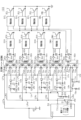
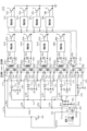
- FIG. 2 is a diagram showing an isolated power supply device
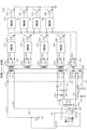
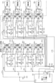
- FIG. 3 is a diagram showing an insulated power supply device according to a modification of the first embodiment
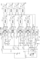
- FIG. 4 is a diagram showing an insulated power supply device according to a modification of the first embodiment
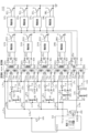
- FIG. 5 is a diagram showing an insulated power supply device according to a modification of the first embodiment
- FIG. 6 is a diagram showing an insulated power supply device according to a modification of the first embodiment
- FIG. 7 is a diagram showing an insulated power supply device according to a modification of the first embodiment
- FIG. 1 is an overall configuration diagram of a motor control system according to a first embodiment
- FIG. 2 is a diagram showing an isolated power supply device
- FIG. 3 is a diagram showing an insulated power supply device according to a modification of the first embodiment
- FIG. 4 is a diagram showing an insulated power supply device according to a modification of the first embodiment
- FIG. 5 is
- FIG. 8 is a diagram showing an insulated power supply device according to a modification of the first embodiment
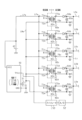
- FIG. 9 is a diagram showing an insulated power supply device according to a second embodiment
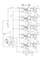
- FIG. 10 is a diagram showing an insulated power supply device according to a modification of the second embodiment.
- the insulated power supply device of this embodiment is installed, for example, in an electric vehicle that includes only a motor generator among a motor generator and an engine.
- the motor control system includes a motor generator 10, an inverter 12, a boost converter 30, and a control device 40.
- Motor generator 10 is connected to drive wheels via a power splitting mechanism (not shown).
- the motor generator 10 is connected to an inverter 12 and serves as a vehicle main engine.
- the inverter 12 is a three-phase inverter, and is connected to a high voltage battery 20 (for example, a lithium ion secondary voltage battery or a nickel metal hydride secondary battery) via a boost converter 30.
- the boost converter 30 includes a smoothing capacitor 31, a reactor 32, an upper arm boost switch SCH, and a lower arm boost switch SCL.
- voltage-controlled semiconductor switches are used as the upper arm boost switch SCH and the lower arm boost switch SCL, and specifically, IGBTs are used.
- a freewheeling diode is connected antiparallel to each switch SCH, SCL.
- the emitter of the upper arm boost switch SCH is connected to the collector of the lower arm boost switch SCL.
- a first end of a smoothing capacitor 31 is connected to the collector of the upper arm boost switch SCH, and a second end of the smoothing capacitor 31 and a negative terminal of the high voltage battery 20 are connected to the emitter of the lower arm boost switch SCL.
- the series connection body of each step-up switch SCH, SCL is connected in parallel to the smoothing capacitor 31.
- the emitter of the upper arm boost switch SCH and the collector of the lower arm boost switch SCL are connected to the positive terminal of the high voltage battery 20 via the reactor 32.
- Boost converter 30 boosts the output voltage of high voltage battery 20 by turning on and off each boost switch SCH, SCL.
- the inverter 12 includes three phases of series-connected bodies of upper arm switches SUH, SVH, and SWH and lower arm switches SUL, SVL, and SWL.
- voltage-controlled semiconductor switches are used as each of the switches SUH to SWL, and specifically, IGBTs are used.
- Freewheel diodes are connected in antiparallel to each of the switches SUH to SWL.
- the emitter of the U-phase upper arm switch SUH is connected to the collector of the U-phase lower arm switch SUL.
- a connection point between the U-phase upper arm switch SUH and the U-phase lower arm switch SUL is connected to the U-phase input terminal of the motor generator 10 .
- the emitter of the V-phase upper arm switch SVH is connected to the collector of the V-phase lower arm switch SVL.
- a connection point between the V-phase upper arm switch SVH and the V-phase lower arm switch SVL is connected to the V-phase input terminal of the motor generator 10.
- the emitter of the W-phase upper arm switch SWH is connected to the collector of the W-phase lower arm switch SWL.
- a connection point between the W-phase upper arm switch SWH and the W-phase lower arm switch SWL is connected to the W-phase input terminal of the motor generator 10 .
- the collectors of each of the upper arm switches SUH to SWH are connected by a positive bus bar 13 such as a bus bar.
- the positive side bus bar 13 is connected to the collector of the upper arm boost switch SCH and the first end of the smoothing capacitor 31.
- the emitters of each of the lower arm switches SUL to SWL are connected by a negative bus bar 14 such as a bus bar.
- the negative bus 14 is connected to the emitter of the lower arm boost switch SCL, the second end of the smoothing capacitor 31, and the negative terminal of the high voltage battery 20.
- the control device 40 is a microcomputer driven by power supplied from a low voltage battery 42 as a DC power source.
- Control device 40 operates inverter 12 and boost converter 30 to control the torque of motor generator 10 to command torque Trq*.
- the control device 40 generates operation signals GUH to GWL and outputs them to the drive circuits of the switches SUH to SWL in order to turn on and off the switches SUH to SWL constituting the inverter 12.
- the control device 40 generates operation signals GCH, GCH and outputs them to the drive circuits of the switches SCH, SCL in order to turn on/off the switches SCH, SCL constituting the boost converter 30.
- the low-voltage battery 42 is a storage battery whose output voltage is lower than the output voltage of the high-voltage battery 20, and is, for example, a lead-acid battery. In this embodiment, the low voltage battery 42 corresponds to a "DC power source".
- the interface section 44 electrically insulates a high voltage region including the motor generator 10, inverter 12, boost converter 30, and high voltage battery 20 from a low voltage region including the control device 40 and the low voltage battery 42, and connects these regions. It has the function of transmitting signals between systems.
- the interface section 44 is, for example, a photocoupler.
- the insulated power supply device 100 has a function of supplying power to drive circuits DCH, DCL, DUH to DWL that drive the switches SCH, SCL, SUH to SWL while insulating between a high voltage region and a low voltage region.
- the insulated power supply device 100 is a flyback switching power supply.
- the insulated power supply device 100 includes a power supply IC 50 and a control switch 51.
- the power supply IC 50 and the control switch 51 are provided in a low voltage region.
- the power supply IC 50 turns the control switch 51 on and off.
- the control switch 51 is a voltage-controlled semiconductor switch, specifically an N-channel MOSFET.
- the isolated power supply device 100 includes an upper arm transformer that supplies power to each upper arm drive circuit DCH, DUH, DVH, and DWH, and a lower arm transformer that supplies power to each lower arm drive circuit DCL, DUL, DVL, and DWL. It is equipped with The upper arm transformer is individually provided corresponding to each upper arm switch SCH, SUH, SVH, and SWH. The lower arm transformer is provided as a common transformer for each lower arm switch SCL, SUL, SVL, and SWL.
- the upper arm transformers are the first to fourth transformers 60a, 60b, 60c, and 60d
- the lower arm transformer is the fifth transformer 60e.
- the first transformer 60a supplies power to the boosting upper arm drive circuit DCH
- the second transformer 60b supplies power to the U-phase upper arm drive circuit DUH
- the third transformer 60c supplies power to the V-phase upper arm drive circuit DVH
- the fourth transformer 60d supplies power to the W-phase upper arm drive circuit DWH.
- the fifth transformer 60e supplies power to each lower arm drive circuit DCL, DUL, DVL, and DWL. Note that in this embodiment, each drive circuit DCH, DCL, DUH to DWL corresponds to a "power supply target".
- the first transformer 60a includes a first input winding 61a, a first output winding 62a, and a first feedback winding 63a.
- the first transformer 60a includes a common core around which windings 61a, 62a, and 63a are wound, and the windings 61a, 62a, and 63a are magnetically coupled through the common core.
- the second transformer 60b like the first transformer 60a, includes a second input winding 61b, a second output winding 62b, and a second feedback winding 63b that are magnetically coupled through a common core.
- the third transformer 60c like the first transformer 60a, includes a third input winding 61c, a third output winding 62c, and a third feedback winding 63c that are magnetically coupled by a common core.
- the fourth transformer 60d like the first transformer 60a, includes a fourth input winding 61d, a fourth output winding 62d, and a fourth feedback winding 63d, which are magnetically coupled through a common core.
- the fifth transformer 60e includes a fifth input winding 61e, a fifth output winding 62e, and a fifth feedback winding 63e, which are magnetically coupled by a common core.
- each input winding 61a to 61e and each feedback winding 63a to 63e are provided in a low voltage region.
- Each output winding 62a to 62e is provided in a high voltage region.
- Each transformer 60a to 60e is provided with a plurality of terminals.
- Corresponding first to fifth output windings 62a to 62e are connected to output terminals of the first to fifth transformers 60a to 60e.
- the first terminal T1a of the first transformer 60a is connected to the second terminal T2a of the first transformer 60a via the first input winding 61a.
- the third terminal T3a of the first transformer 60a is connected to the fourth terminal T4a of the first transformer 60a via the first feedback winding 63a.
- the potential of the first terminal T1a with respect to the second terminal T2a of the first transformer 60a becomes higher, the potential of the fourth terminal T4a of the first feedback winding 63a becomes higher than that of the third terminal T3a of the first transformer 60a. An induced voltage like this is generated.
- the first terminal T1b of the second transformer 60b is connected to the second terminal T2b of the second transformer 60b via the second input winding 61b.
- the third terminal T3b of the second transformer 60b is connected to the fourth terminal T4b of the second transformer 60b via the second feedback winding 63b.
- the potential of the first terminal T1b with respect to the second terminal T2b of the second transformer 60b becomes higher, the potential of the fourth terminal T4b of the second feedback winding 63b becomes higher than that of the third terminal T3b of the second transformer 60b. An induced voltage like this is generated.
- the first terminal T1c of the third transformer 60c is connected to the second terminal T2c of the third transformer 60c via the third input winding 61c.
- the third terminal T3c of the third transformer 60c is connected to the fourth terminal T4c of the third transformer 60c via the third feedback winding 63c.
- the potential of the first terminal T1c with respect to the second terminal T2c of the third transformer 60c becomes higher, the potential of the fourth terminal T4c of the third feedback winding 63c becomes higher than that of the third terminal T3c of the third transformer 60c. An induced voltage like this is generated.
- the first terminal T1d of the fourth transformer 60d is connected to the second terminal T2d of the fourth transformer 60d via the fourth input winding 61d.
- the third terminal T3d of the fourth transformer 60d is connected to the fourth terminal T4d of the fourth transformer 60d via the fourth feedback winding 63d.
- the potential of the first terminal T1d with respect to the second terminal T2d of the fourth transformer 60d becomes higher, the potential of the fourth terminal T4d of the fourth feedback winding 63d becomes higher than that of the third terminal T3d of the fourth transformer 60d. An induced voltage like this is generated.
- the first terminal T1e of the fifth transformer 60e is connected to the second terminal T2e of the fifth transformer 60e via the fifth input winding 61e.
- the third terminal T3e of the fifth transformer 60e is connected to the fourth terminal T4e of the fifth transformer 60e via the fifth feedback winding 63e.
- the potential of the first terminal T1e with respect to the second terminal T2e of the fifth transformer 60e becomes higher, the potential of the fourth terminal T4e of the fifth feedback winding 63e becomes higher than that of the third terminal T3e of the fifth transformer 60e. An induced voltage like this is generated.
- the output terminal of the first transformer 60a is connected to the boosting upper arm drive circuit DCH via a first output diode 64a and a first output capacitor 65a.
- the output terminal of the second transformer 60b is connected to the U-phase upper arm drive circuit DUH via a second output diode 64b and a second output capacitor 65b.
- the output terminal of the third transformer 60c is connected to the V-phase upper arm drive circuit DVH via a third output diode 64c and a third output capacitor 65c.
- the output terminal of the fourth transformer 60d is connected to the W-phase upper arm drive circuit DWH via a fourth output diode 64d and a fourth output capacitor 65d.
- the output terminal of the fifth transformer 60e is connected to each lower arm drive circuit DCL, DUL, DVL, and DWL via a fifth output diode 64e and a fifth output capacitor 65e.
- the first terminals T1a to T1e of each transformer 60a to 60e are connected to the positive terminal of the low voltage battery 42 via wiring.
- the first terminal T1e of the fifth transformer 60e is connected to the positive terminal of the low voltage battery 42 via the fifth positive wiring LPe.
- the first terminal T1a of the first transformer 60a is connected to the fifth positive wiring LPe via the first positive wiring LPa. That is, the first terminal T1a of the first transformer 60a is connected to the positive terminal of the low voltage battery 42 via the first and fifth positive electrode wirings LPa and LPe.
- the first terminals T1b to T1d of the second to fourth transformers 60b to 60d are connected to the fifth positive electrode via the corresponding second to fourth positive electrode wirings LPb to LPd. It is connected to the wiring LPe. That is, the first terminals T1b to T1d of the second to fourth transformers 60b to 60d are connected to the positive terminals of the low voltage battery 42 via the fifth positive wiring LPe and the corresponding second to fourth positive wirings LPb to LPd. It is connected. Note that the negative electrode side of the low voltage battery 42 is connected to ground.
- the second terminals T2a to T2e of each transformer 60a to 60e are connected to the drain of the control switch 51 via wiring.
- the second terminal T2a of the first transformer 60a is connected to the drain of the control switch 51 via the first negative wiring LNa.
- Second terminals T2b to T2d of the second to fifth transformers 60b to 60e are connected to the first negative wiring LNa via corresponding second to fifth negative wirings LNb to LNd. That is, the second terminals T2b to T2d of the second to fifth transformers 60b to 60e are connected to the drain of the control switch 51 via the first negative wiring LNa and the corresponding second to fifth negative wiring LNb to LNd. has been done.
- the source of the control switch 51 is connected to ground.
- the third terminals T3a to T3e of the first to fifth transformers 60a to 60e are connected to the input side common wiring Ls via the corresponding first to fifth feedback wirings LRa to LRe.
- Each of the feedback wirings LRa to LRe and the input side common wiring Ls are provided in a low voltage region.
- a first feedback diode 71a is provided in the first feedback wiring LRa.
- the anode of the first feedback diode 71a is connected to the third terminal T3a of the first transformer 60a, and the cathode of the first feedback diode 71a is connected to the input side common wiring Ls.
- a second feedback diode 71b is provided on the second feedback wiring LRb.
- the anode of the second feedback diode 71b is connected to the third terminal T3b of the second transformer 60b, and the cathode of the second feedback diode 71b is connected to the input side common wiring Ls.
- a third feedback diode 71c is provided in the third feedback wiring LRc.
- the anode of the third feedback diode 71c is connected to the third terminal T3c of the third transformer 60c, and the cathode of the third feedback diode 71c is connected to the input side common wiring Ls.
- a fourth feedback diode 71d is provided on the fourth feedback wiring LRd.
- the anode of the fourth feedback diode 71d is connected to the third terminal T3d of the fourth transformer 60d, and the cathode of the fourth feedback diode 71d is connected to the input side common wiring Ls.
- a fifth feedback diode 71e is provided in the fifth feedback wiring LRe.
- the anode of the fifth feedback diode 71e is connected to the third terminal T3e of the fifth transformer 60e, and the cathode of the fifth feedback diode 71e is connected to the input side common wiring Ls.
- the fourth terminal T4a of the first transformer 60a is connected to the ground via the first ground wiring LGa.
- the fourth terminals T4b to T4e of the second to fifth transformers 60b to 60e are connected to the ground via the corresponding second to fifth ground wirings LGb to LGe. .
- the insulated power supply device 100 includes first to fifth feedback capacitors 72a to 72e.
- the first feedback capacitor 72a connects the cathode of the first feedback diode 71a and the first ground wiring LGa.
- the second to fifth feedback capacitors 72b to 72e connect the cathodes of the corresponding second to fifth feedback diodes 71b to 71e and the corresponding second to fifth ground wirings LGb to Connect with LGe.
- the insulated power supply device 100 includes a bleeder resistor.
- the bleeder resistor is a resistor that is provided to adjust the magnitude of the load connected to each transformer 60a to 60e, and plays a role in reducing variations in voltage generated in each feedback winding 63a to 63e.
- the insulated power supply device 100 includes first to fourth bleeder resistors 73a to 73d as upper arm bleeder resistors and a fifth bleeder resistor 73e as a lower arm bleeder resistor. There is.
- the resistance value of the fifth bleeder resistor 73e is set smaller than the resistance value of the first to fourth bleeder resistors 73a to 73d.
- a first end of the first bleeder resistor 73a is connected to the first feedback wiring LRa, and a second end of the first bleeder resistor 73a is connected to ground.
- the first ends of the second to fifth bleeder resistors 73b to 73e are connected to the corresponding second to fifth feedback wirings LRb to LRe, and The second ends of the bleeder resistors 73b to 73e are connected to ground.
- the first end of each bleeder resistor 73a to 73e is connected to the cathode of the corresponding feedback diode 71a to 71e.
- the power supply IC 50 is one integrated circuit, and electrically insulates between the low voltage battery 42 and each drive circuit DCH, DCL, DUH to DWL, and connects the low voltage battery 42 to each drive circuit DCH, DCL, DUH.
- the control switch 51 is turned on and off in order to supply power to ⁇ DWL.
- the power supply IC 50 turns on and off the control switch 51 to feedback control the feedback control value Vfb to the target value Vtg.
- the power supply IC 50 sets a duty ratio Ton/Tsw where one switching period in the control switch 51 is Tsw and the on time is Ton. Then, an operation signal corresponding to the set duty ratio is output to the gate of the control switch 51.
- the power supply IC 50 corresponds to a "control unit".
- the control switch 51 When the control switch 51 is turned on, power is supplied from the low voltage battery 42 to each input winding 61a to 61e. During this time, an induced voltage is generated in the first feedback winding 63a such that the potential of the fourth terminal T4a of the first transformer 60a is higher than that of the third terminal T3a. In this case, the first feedback diode 71a restricts the flow of current to the first feedback winding 63a, and magnetic energy is accumulated in the first transformer 60a. Note that, as in the case of the first feedback winding 63a, the flow of current to the first output winding 62a is regulated by the first output diode 64a.
- the control switch 51 when the control switch 51 is turned on, magnetic energy is accumulated in the second to fifth transformers 60b to 60e. Specifically, when the control switch 51 is turned on, an induced voltage is generated in the second feedback winding 63b such that the potential of the fourth terminal T4b of the second transformer 60b is higher than that of the third terminal T3b. Occur. In this case, the second feedback diode 71b restricts the flow of current to the second feedback winding 63b, and magnetic energy is accumulated in the second transformer 60b.
- the control switch 51 When the control switch 51 is turned on, an induced voltage is generated in the third feedback winding 63c such that the potential of the fourth terminal T4c of the third transformer 60c is higher than that of the third terminal T3c.
- the third feedback diode 71c restricts the flow of current to the third feedback winding 63c, and magnetic energy is accumulated in the third transformer 60c.
- control switch 51 when the control switch 51 is turned on, current flows through the second to fifth output windings 62b to 62e, as in the case of the second to fifth feedback windings 63b to 63e. It is regulated by the second to fifth output diodes 64b to 64e.
- the first transformer 60a corresponding to the boosting upper arm drive circuit DCH supplies more magnetic energy than the second to fourth transformers 60b to 60d corresponding to the upper arm drive circuits DUH to DWH of each phase.
- the output voltage will increase due to the excess.
- the switches SUH to SWL of the inverter 12 only the U- and V-phase upper and lower arm switches SUH, SVH, SUL, and SVL may be driven.
- the magnitude of the load on the U- and V-phase upper and lower arm drive circuits DUH, DVH, DUL, and DVL is greater than the magnitude of the load on the W-phase upper and lower arm drive circuits DWH and DWL.
- the second and third transformers 60b and 60c corresponding to the U and V phase upper arm drive circuits DUH and DVH have lower magnetic energy than the fourth transformer 60d corresponding to the W phase upper arm drive circuit DWH.
- the control switch 51 may be turned on or off based on the output voltage of any one of the transformers 60a to 60e.
- the control switch 51 in the transformer to be controlled among the transformers 60a to 60e, the control switch 51 is turned on and off so that the output voltage becomes the target output voltage.
- the output voltage changes by the difference between the output voltage of the controlled transformer and the target output voltage. Therefore, in a situation where there is a possibility that variations occur in the output voltages of the transformers 60a to 60e described above, the output voltage of the transformers that are not controlled among the transformers 60a to 60e may become excessively high with respect to the target output voltage.
- the output voltage of each transformer 60a to 60e is the voltage generated in each output winding 62a to 62e
- the target output voltage is defined by the upper limit voltage and lower limit voltage of the voltage generated in each output winding 62a to 62e. set within the specified voltage range.
- the insulated power supply device 100 uses the voltages generated in each of the feedback windings 63a to 63e to turn on and off the control switch 51.
- the insulated power supply device 100 includes a first voltage dividing resistor 84 and a second voltage dividing resistor 85.
- a first end of the first voltage dividing resistor 84 is connected to the input side common line Ls, and a second end of the first voltage dividing resistor 84 is connected to a first end of the second voltage dividing resistor 85.
- the second end of the second voltage dividing resistor 85 is connected to ground.
- a connection point between the second end of the first voltage dividing resistor 84 and the first end of the second voltage dividing resistor 85 is connected to the power supply IC 50.
- the power supply IC 50 turns on and off the control switch 51 based on the voltage value of the input side common wiring Ls.
- the power supply IC 50 obtains the divided voltage values of the first and second voltage dividing resistors 84 and 85.
- the power supply IC 50 sets the duty ratio of the control switch 51 based on the obtained partial pressure value.
- the duty ratio of the control switch 51 is set based on the voltage generated in any one of the feedback windings of each transformer 60a to 60e, the voltage generated in many feedback windings is used for control purposes. It is used to set the duty ratio of the switch 51.
- each transformer 60a to 60e the magnetic energy stored in each transformer 60a to 60e is exchanged between each transformer 60a to 60e.
- a closed circuit including each of the feedback windings 63a to 63e, each of the feedback wirings LRa to LRe, and the input side common wiring Ls is formed.
- magnetic energy is transmitted between the transformers 60a to 60e from a transformer with high magnetic energy to a transformer with low magnetic energy as a result of current flowing in the closed circuit. This prevents excessive or insufficient magnetic energy from being stored in each of the transformers 60a to 60e. Therefore, variations in the output voltage of each transformer 60a to 60e can be reduced.
- each feedback diode 71a to 71e and each feedback capacitor 72a to 72e are provided corresponding to each feedback winding 63a to 63e.
- the current output from the third terminal T3a-T3e of each transformer 60a-60e is rectified by the corresponding feedback diode 71a-71e, and the corresponding feedback capacitor 72a-72e is charged.
- a current flows as the charges accumulated in each of the feedback capacitors 72a to 72e are exchanged. .
- magnetic energy is exchanged between each of the transformers 60a to 60e.
- each of the feedback windings 63a to 63e corresponds to a "control winding”
- each of the feedback wirings LRa to LRe corresponds to a "control wiring”.
- the variation in the output voltage of each transformer 60a to 60e is reduced, and compared to the case where one of the transformers 60a to 60e is provided with a feedback winding, a transformer that is not to be controlled.
- the number of As a result, the output voltage of each transformer 60a to 60e can be prevented from becoming excessively high or low, and as a result, the controllability of the output voltage of each transformer 60a to 60e can be improved.
- feedback windings 63a to 63e are provided corresponding to each transformer 60a to 60e.
- Third terminals T3a to T3e of each transformer 60a to 60e are connected to the input side common wiring Ls via corresponding feedback wiring LRa to LRe. Then, the voltage value of the input side common wiring Ls is transmitted to the power supply IC 50. Therefore, since there is no need to add an insulated transmission section, an increase in the number of components of the insulated power supply device 100 can be suppressed.
- the controllability of the output voltage of each transformer 60a to 60e can be improved as described above. In other words, the controllability of the output voltage of each transformer 60a to 60e can be improved while suppressing an increase in the number of components of the insulated power supply device 100.
- each feedback winding 63a to 63e When a current flows in a closed circuit including each feedback winding 63a to 63e, each feedback wiring LRa to LRe, and the input side common wiring Ls, it is difficult for the current to flow in the closed circuit due to the inductance component of each feedback winding 63a to 63e. There are some concerns. In this case, there is a concern that the magnetic energy stored in each of the transformers 60a to 60e may not be sufficiently exchanged.
- the electric charges accumulated in the feedback capacitors 72a to 72e are transferred and received in a closed circuit including each of the feedback windings 63a to 63e, each of the feedback wirings LRa to LRe, and the input side common wiring Ls.
- a current flows.
- the magnetic energy stored in each transformer 60a to 60e is exchanged. Therefore, magnetic energy can be suitably transferred between the transformers 60a to 60e while suppressing the inductance components of the feedback windings 63a to 63e from preventing current from flowing in the closed circuit.
- a closed circuit including each of the feedback windings 63a to 63e, each of the feedback wirings LRa to LRe, and the input side common wiring Ls is formed without using the first and second voltage dividing resistors 84 and 85. Therefore, compared to a configuration in which a voltage dividing resistor is provided corresponding to each of the feedback windings 63a to 63e, it is possible to suppress the current from flowing through the closed circuit.
- each of the transformers 60a to 60e is transferred by flowing current through a closed circuit including a bleeder resistor, which is a heat generating component.
- a closed circuit including a bleeder resistor which is a heat generating component.
- the bleeder resistor be placed near each of the feedback windings 63a to 63e.
- each of the feedback windings 63a to 63e is connected to the input side common wiring Ls via each of the feedback wirings LRa to LRe.
- the bleeder resistor when the bleeder resistor is connected to each of the feedback wirings LRa to LRe that are directly connected to each of the feedback windings 63a to 63e, the bleeder resistance It is contemplated that the body could be placed close to each return winding 63a-63e.
- each bleeder resistor 73a to 73e is connected to the corresponding feedback wiring LRa to LRe. Therefore, each of the bleeder resistors 73a to 73e can be arranged while suppressing the length of the closed circuit path including each of the bleeder resistors 73a to 73e.
- a bleeder resistor is provided corresponding to each of the feedback windings 63a to 63e. Specifically, each bleeder resistor 73a to 73e corresponding to each feedback wiring LRa to LRe is connected. Thereby, the bleeder resistors 73a to 73e, which are heat generating components, can be arranged in a distributed manner.
- the first to fourth transformers 60a to 60d are individually provided corresponding to the upper arm switches SCH, SUH, SVH, and SWH, and the fifth transformer 60e is provided to each of the lower arm switches SCL, SUL, SVL, and SWL. It is installed as a common transformer. In this configuration, the magnitude of the load connected to the fifth transformer 60e is considered to be larger than the magnitude of the load connected to the first to fourth transformers 60a to 60d.
- the resistance value of the fifth bleeder resistor 73e is made smaller than the resistance value of the first to fourth bleeder resistors 73a to 73d.
- the upper arm transformer is a common transformer for each upper arm switch SCH, SUH, SVH, SWH instead of being individually provided corresponding to each upper arm switch SCH, SUH, SVH, SWH. It may be provided as
- the upper arm transformer is the sixth transformer 60f.
- the sixth transformer 60f supplies power to each upper arm drive circuit DCH, DUH to DWH.
- the sixth transformer 60f includes a sixth input winding 61f and a sixth feedback winding 63f.
- the sixth transformer 60f includes a common core around which a sixth input winding 61f, each output winding 62a to 62d, and a sixth feedback winding 63f are wound. Magnetically coupled by the core.
- FIG. 3 the same components as those shown in FIG. 2 are given the same reference numerals for convenience.
- the sixth transformer 60f is provided with first to fourth terminals T1f to T4f.
- the first terminal T1f of the sixth transformer 60f is connected to the second terminal T2f of the sixth transformer 60f via the sixth input winding 61f.
- the third terminal T3f of the sixth transformer 60f is connected to the fourth terminal T4f of the sixth transformer 60f via the sixth feedback winding 63f.
- the potential of the first terminal T1f with respect to the second terminal T2f of the sixth transformer 60f becomes higher, the potential of the fourth terminal T4f of the sixth feedback winding 63f becomes higher than that of the third terminal T3f of the sixth transformer 60f. An induced voltage like this is generated.
- the first terminal T1f of the sixth transformer 60f is connected to the positive terminal of the low voltage battery 42 via the first and fifth positive wiring LPa, LPe.
- the second terminal T2f of the sixth transformer 60f is connected to the drain of the control switch 51 via the first negative wiring LNa.
- the third terminal T3f of the sixth transformer 60f is connected to the input side common wiring Ls via the fourth feedback wiring LRd.
- the fourth terminal T4f of the sixth transformer 60f is connected to the ground via the fourth ground wiring LGd.
- the sixth transformer 60f is provided as the upper arm transformer.
- the number of transformers provided as upper arm transformers can be reduced compared to a configuration in which the first to fourth transformers 60a to 60d are provided.
- the number of transformers that are not subject to control can be reduced.
- feedback windings 63a to 63e may be provided corresponding to at least two of each transformer 60a to 60e.
- the first, third, fourth and fifth transformers correspond to the first, third, fourth and fifth transformers 60a, 60c, 60d and 60e.
- Five feedback windings 63a, 63c, 63d, and 63e are provided, and the second transformer 60b may not be provided with a feedback winding.
- the same components as those shown in FIG. 2 are given the same reference numerals for convenience.
- the number of transformers provided with feedback windings is reduced compared to a configuration in which feedback windings 63a to 63e are provided corresponding to each transformer 60a to 60e.
- a feedback winding is connected to any one of the transformers 60a to 60e.
- the number of transformers that are not subject to control can be reduced compared to a configuration in which a transformer is provided. As a result, the number of components of the insulated power supply device 100 can be reduced, and the controllability of the output voltages of the first, third, fourth, and fifth transformers 60a, 60c, 60d, and 60e can be improved.
- the insulated power supply device 100 includes third to twelfth voltage dividing resistors 86 to 95.
- the same components as those shown in FIG. 2 are given the same reference numerals for convenience.
- the third voltage dividing resistor 86 and the fourth voltage dividing resistor 87 are provided corresponding to the first feedback wiring LRa.
- the first end of the third voltage dividing resistor 86 is connected to the first feedback wiring LRa, and the second end of the third voltage dividing resistor 86 is connected to the input side common wiring Ls and the first end of the fourth voltage dividing resistor 87. It is connected to the.
- the second end of the fourth voltage dividing resistor 87 is connected to ground.
- the fifth voltage dividing resistor 88 and the sixth voltage dividing resistor 89 are provided corresponding to the second feedback wiring LRb.
- the first end of the fifth voltage dividing resistor 88 is connected to the second feedback wiring LRb, and the second end of the fifth voltage dividing resistor 88 is connected to the input side common wiring Ls and the first end of the sixth voltage dividing resistor 89. It is connected to the.
- the second end of the sixth voltage dividing resistor 89 is connected to ground.
- the seventh voltage dividing resistor 90 and the eighth voltage dividing resistor 91 are provided corresponding to the third feedback wiring LRc.
- the first end of the seventh voltage dividing resistor 90 is connected to the third feedback wiring LRc, and the second end of the seventh voltage dividing resistor 90 is connected to the input side common wiring Ls and the first end of the eighth voltage dividing resistor 91. It is connected to the.
- the second part of the eighth voltage dividing resistor 91 is connected to ground.
- the ninth voltage dividing resistor 92 and the tenth voltage dividing resistor 93 are provided corresponding to the fourth feedback wiring LRd.
- the first end of the ninth voltage dividing resistor 92 is connected to the fourth feedback wiring LRd, and the second end of the ninth voltage dividing resistor 92 is connected to the input side common wiring Ls and the first end of the tenth voltage dividing resistor 93. It is connected to the.
- the second end of the tenth voltage dividing resistor 93 is connected to ground.
- the eleventh voltage dividing resistor 94 and the twelfth voltage dividing resistor 95 are provided corresponding to the fifth feedback wiring LRe.
- the first end of the eleventh voltage dividing resistor 94 is connected to the fifth feedback wiring LRe, and the second end of the eleventh voltage dividing resistor 94 is connected to the input side common wiring Ls and the first end of the twelfth voltage dividing resistor 95. It is connected to the.
- the second end of the twelfth voltage dividing resistor 95 is connected to ground.
- the insulated power supply device 100 may be provided with a first common wiring Ls1 and a second common wiring Ls2.
- the first common wiring Ls1 corresponds to the input side common wiring Ls in FIG. 2 described above.
- the second common wiring Ls2 is connected to each of the feedback wirings LRa to LRe.
- the third terminals T3a to T3e of each transformer 60a to 60e are connected via a second common wiring Ls2.
- the anodes of each of the feedback diodes 71a to 71e are connected to the second common wiring Ls2.
- FIG. 6 the same components as those shown in FIG. 2 are given the same reference numerals for convenience.
- the path of the first closed circuit including each of the feedback windings 63a to 63e, each of the feedback wirings LRa to LRe, and the first common wiring Ls1 becomes longer, the amount of voltage drop in the first closed circuit increases, There is a concern that it becomes difficult for current to flow through the first closed circuit.
- the third terminals T3a to T3e of each transformer 60a to 60e are connected via the second common wiring Ls2.
- a second closed circuit including each of the feedback windings 63a to 63e and the second common wiring Ls2 is formed.
- the path of the second closed circuit is prevented from becoming longer than the path of the first closed circuit. Therefore, the magnetic energy stored in each of the transformers 60a to 60e can be transferred while suppressing an increase in the amount of voltage drop in the closed circuit.
- the bleeder resistor may be connected to the input side common wiring Ls.
- the insulated power supply device 100 includes a common bleeder resistor 74.
- a first end of the common bleeder resistor 74 is connected to the input side common wiring Ls, and a second end of the common bleeder resistor 74 is connected to ground.
- the same components as those shown in FIG. 2 are given the same reference numerals for convenience.
- the first end of the common bleeder resistor 74 is connected to the input side common wiring Ls.
- the number of bleeder resistors is reduced compared to the case where a bleeder resistor is connected to each feedback wiring LRa to LRe. be able to.
- the bleeder resistor is not limited to being provided corresponding to each feedback winding 63a to 63e, but may be provided corresponding to any one, two, three, or four of each feedback winding 63a to 63e. may be provided.
- Each of the switches SCH, SCL, SUH to SWL constituting the inverter 12 and the boost converter 30 is not limited to an IGBT, but may be an N-channel MOSFET made of Si, for example.
- the lower arm transformer is not limited to a common transformer for each lower arm switch SCL, SUL, SVL, SWL, but may be individually provided for each lower arm switch SCL, SUL, SVL, SWL, for example. It may also be a transformer. If the lower arm transformer is provided individually, each switch SCH, SCL, SUH to SWL may be made of SiC (silicon carbide) material, GaN (gallium nitride) material, etc. instead of IGBT. A possible case is a configured N-channel MOSFET.
- the insulated power supply device 100 includes seventh to tenth transformers 60g to 60j as lower arm transformers.
- the same components as those shown in FIG. 2 are given the same reference numerals for convenience.
- illustrations of the switches SCH, SCL, SUH to SWL, etc. are omitted.
- the seventh transformer 60g supplies power to the boosting lower arm drive circuit DCL
- the eighth transformer 60h supplies power to the U-phase lower arm drive circuit DUL.
- the ninth transformer 60i supplies power to the V-phase lower arm drive circuit DVL
- the tenth transformer 60j supplies power to the W-phase lower arm drive circuit DWL.
- the seventh transformer 60g includes a seventh input winding 61g, a seventh output winding 62g, and a seventh feedback winding 63g that are magnetically coupled by a common core.
- the eighth transformer 60h includes an eighth input winding 61h, an eighth output winding 62h, and an eighth feedback winding 63h that are magnetically coupled by a common core.
- the ninth transformer 60i includes a ninth input winding 61i, a ninth output winding 62i, and a ninth feedback winding 63i that are magnetically coupled by a common core.
- the tenth transformer 60j includes a tenth input winding 61j, a tenth output winding 62j, and a tenth feedback winding 63j that are magnetically coupled through a common core.
- the seventh to tenth input windings 61g to 61j and the seventh to tenth feedback windings 63g to 63j are provided in a low voltage region.
- the seventh to tenth output windings 62g to 62j are provided in a high voltage region.
- the output terminal of the seventh transformer 60g is connected to the boosting lower arm drive circuit DCL via the seventh output diode 64g and the seventh output capacitor 65g.
- the output terminal of the eighth transformer 60h is connected to the U-phase lower arm drive circuit DUL via an eighth output diode 64h and an eighth output capacitor 65h.
- the output terminal of the ninth transformer 60i is connected to the V-phase lower arm drive circuit DVL via the ninth output diode 64i and the ninth output capacitor 65i.
- the output terminal of the tenth transformer 60j is connected to the W-phase lower arm drive circuit DWL via the tenth output diode 64j and the tenth output capacitor 65j.
- the seventh transformer 60g is provided with first to fourth terminals T1g to T4g.
- the first terminal T1g of the seventh transformer 60g is connected to the second terminal T2g of the seventh transformer 60g via the seventh input winding 61g.
- the third terminal T3g of the seventh transformer 60g is connected to the fourth terminal T4g of the seventh transformer 60g via the seventh feedback winding 63g.
- the potential of the first terminal T1g with respect to the second terminal T2g of the seventh transformer 60g becomes higher, the potential of the fourth terminal T4g of the seventh feedback winding 63g becomes higher than that of the third terminal T3g of the seventh transformer 60g. An induced voltage like this is generated.
- the eighth transformer 60h is provided with first to fourth terminals T1h to T4h.
- the first terminal T1h of the eighth transformer 60h is connected to the second terminal T2h of the eighth transformer 60h via the eighth input winding 61h.
- the third terminal T3h of the eighth transformer 60h is connected to the fourth terminal T4h of the eighth transformer 60h via the eighth feedback winding 63h.
- the potential of the first terminal T1h with respect to the second terminal T2h of the eighth transformer 60h becomes higher, the potential of the fourth terminal T4h of the eighth feedback winding 63h becomes higher than that of the third terminal T3h of the eighth transformer 60h. An induced voltage like this is generated.
- the ninth transformer 60i is provided with first to fourth terminals T1i to T4i.
- the first terminal T1i of the ninth transformer 60i is connected to the second terminal T2i of the ninth transformer 60i via the ninth input winding 61i.
- the third terminal T3i of the ninth transformer 60i is connected to the fourth terminal T4i of the ninth transformer 60i via the ninth feedback winding 63i.
- the potential of the first terminal T1i with respect to the second terminal T2i of the ninth transformer 60i becomes higher, the potential of the fourth terminal T4i of the ninth feedback winding 63i becomes higher than that of the third terminal T3i of the ninth transformer 60i. An induced voltage like this is generated.
- the tenth transformer 60j is provided with first to fourth terminals T1j to T4j.
- the first terminal T1j of the tenth transformer 60j is connected to the second terminal T2j of the tenth transformer 60j via the tenth input winding 61j.
- the third terminal T3j of the tenth transformer 60j is connected to the fourth terminal T4j of the tenth transformer 60j via the tenth feedback winding 63j.
- the first terminal T1g of the seventh transformer 60g is connected to the positive terminal of the low voltage battery 42 via the fifth positive wiring LPe.
- the second terminal T2g of the seventh transformer 60g is connected to the drain of the control switch 51 via the first and fifth negative electrode wirings LNa and LNe.
- the third terminal T3g of the seventh transformer 60g is connected to the input side common wiring Ls via the seventh feedback wiring LRg.
- the fourth terminal T4g of the seventh transformer 60g is connected to the ground via the seventh ground wiring LGg.
- the first terminal T1h of the eighth transformer 60h is connected to the fifth positive wiring LPe via the eighth positive wiring LPh. That is, the first terminal T1h of the eighth transformer 60h is connected to the positive terminal of the low voltage battery 42 via the fifth and eighth positive electrode wirings LPe and LPh.
- the second terminal T2h of the eighth transformer 60h is connected to the fifth negative wiring LNe via the eighth negative wiring LNh. That is, the second terminal T2h of the eighth transformer 60h is connected to the drain of the control switch 51 via the first, fifth, and eighth negative electrode wirings LNa, LNe, and LNh.
- the third terminal T3h of the eighth transformer 60h is connected to the input side common wiring Ls via the eighth feedback wiring LRh.
- the fourth terminal T4h of the eighth transformer 60h is connected to the ground via the eighth ground wiring LGh.
- the first terminal T1i of the ninth transformer 60i is connected to the fifth positive wiring LPe via the ninth positive wiring LPi. That is, the first terminal T1i of the ninth transformer 60i is connected to the positive terminal of the low voltage battery 42 via the fifth and ninth positive electrode wirings LPe and LPi.
- the second terminal T2i of the ninth transformer 60i is connected to the fifth negative wiring LNe via the ninth negative wiring LNi. That is, the second terminal T2i of the ninth transformer 60i is connected to the drain of the control switch 51 via the first, fifth, and ninth negative electrode wirings LNa, LNe, and LNi.
- the third terminal T3i of the ninth transformer 60i is connected to the input side common wiring Ls via the ninth feedback wiring LRi.
- the fourth terminal T4i of the ninth transformer 60i is connected to the ground via the ninth ground wiring LGi.
- the first terminal T1j of the tenth transformer 60j is connected to the fifth positive wiring LPe via the tenth positive wiring LPj.
- the first terminal T1j of the tenth transformer 60j is connected to the positive terminal of the low voltage battery 42 via the fifth and tenth positive wiring LPe, LPj.
- the second terminal T2j of the tenth transformer 60j is connected to the fifth negative wiring LNe via the tenth negative wiring LNj. That is, the second terminal T2j of the tenth transformer 60j is connected to the drain of the control switch 51 via the first, fifth, and tenth negative electrode wirings LNa, LNe, and LNj.
- the third terminal T3j of the tenth transformer 60j is connected to the input side common wiring Ls via the tenth feedback wiring LRj.
- the fourth terminal T4j of the tenth transformer 60j is connected to the ground via the tenth ground wiring LGj.
- a seventh feedback diode 71g is provided on the seventh feedback wiring LRg.
- the anode of the seventh feedback diode 71g is connected to the third terminal T3g of the seventh transformer 60g, and the cathode of the seventh feedback diode 71g is connected to the input side common wiring Ls.
- the eighth feedback wiring LRh is provided with an eighth feedback diode 71h.
- the anode of the eighth feedback diode 71h is connected to the third terminal T3h of the eighth transformer 60h, and the cathode of the eighth feedback diode 71h is connected to the input side common wiring Ls.
- a ninth feedback diode 71i is provided in the ninth feedback wiring LRi.
- the anode of the ninth feedback diode 71i is connected to the third terminal T3i of the ninth transformer 60i, and the cathode of the ninth feedback diode 71i is connected to the input side common wiring Ls.
- a tenth feedback diode 71j is provided on the tenth feedback wiring LRj.
- the anode of the tenth feedback diode 71j is connected to the third terminal T3j of the tenth transformer 60j, and the cathode of the tenth feedback diode 71j is connected to the input side common wiring Ls.
- the insulated power supply device 100 includes seventh to tenth feedback capacitors 72g to 72j.
- the seventh feedback capacitor 72g connects the cathode of the seventh feedback diode 71g and the seventh ground wiring LGg.
- the eighth to tenth feedback capacitors 72h to 72j connect the cathodes of the corresponding eighth to tenth feedback diodes 71h to 71j and the corresponding eighth to tenth ground wirings LGh to Connect with LGj.
- the insulated power supply device 100 includes seventh to tenth bleeder resistors 73g to 73j.
- a first end of the seventh bleeder resistor 73g is connected to the seventh feedback wiring LRg, and a second end of the seventh bleeder resistor 73g is connected to the ground.
- the first ends of the eighth to tenth bleeder resistors 73h to 73j are connected to the corresponding eighth to tenth feedback wirings LRh to LRj, and
- the second ends of the bleeder resistors 73h to 73j are connected to ground.
- the first ends of the seventh to tenth bleeder resistors 73g to 73j are connected to the cathodes of the corresponding feedback diodes 71g to 71j.
- the seventh feedback diode 71g restricts the flow of current to the seventh feedback winding 63g, and magnetic energy is accumulated in the seventh transformer 60g.
- the flow of current to the seventh output winding 62g is regulated by the seventh output diode 64g.
- magnetic energy is accumulated in the eighth to tenth transformers 60h to 60j.
- each transformer 60a-60e has a corresponding input winding 61a-61e and output winding 62a-62e, and no feedback winding.
- FIG. 9 the same components as those shown in FIG. 2 are given the same reference numerals for convenience. Further, in FIG. 9, illustration of each drive circuit DCH, DCL, DUH to DWL, etc. is omitted.
- Each of the transformers 60a to 60e is provided with a fifth terminal T5a to T5e and a sixth terminal T6a to T6e.
- the fifth terminal T5a of the first transformer 60a is connected to the sixth terminal T6a of the first transformer 60a via the first output winding 62a.
- the fifth terminal T5b of the second transformer 60b is connected to the sixth terminal T6b of the second transformer 60b via the second output winding 62b.
- the fifth terminal T5c of the third transformer 60c is connected to the sixth terminal T6c of the third transformer 60c via the third output winding 62c.
- the fifth terminal T5d of the fourth transformer 60d is connected to the sixth terminal T6d of the fourth transformer 60d via the fourth output winding 62d.
- the fifth terminal T5e of the fifth transformer 60e is connected to the sixth terminal T6e of the fifth transformer 60e via the fifth output winding 62e.
- the fifth terminal T5a of the first transformer 60a is connected to the output side common wiring Lt and the boosting upper arm drive circuit DCH via the first output wiring LOa.
- the fifth terminal T5b of the second transformer 60b is connected to the output side common wiring Lt and the U-phase upper arm drive circuit DUH via the second output wiring LOb.
- the fifth terminal T5c of the third transformer 60c is connected to the output side common wiring Lt and the V-phase upper arm drive circuit DVH via the third output wiring LOc.
- the fifth terminal T5d of the fourth transformer 60d is connected to the output side common wiring Lt and the W-phase upper arm drive circuit DWH via the fourth output wiring LOd.
- the fifth terminal T5e of the fifth transformer 60e is connected to the output side common wiring Lt and each of the lower arm drive circuits DCL, DUL, DVL, and DWL via the fifth output wiring LOe.
- Sixth terminals T6a to T6e of each transformer 60a to 60e are connected to ground.
- each output wiring LOa to LOe corresponds to a "control wiring".
- a first output diode 64a is provided on the first output wiring LOa.
- the anode of the first output diode 64a is connected to the fifth terminal T5a of the first transformer 60a, and the cathode of the first output diode 64a is connected to the boosting upper arm drive circuit DCH and the output side common wiring Lt.
- a second output diode 64b is provided on the second output wiring LOb.
- the anode of the second output diode 64b is connected to the fifth terminal T5b of the second transformer 60b, and the cathode of the second output diode 64b is connected to the U-phase upper arm drive circuit DUH and the output side common wiring Lt.
- a third output diode 64c is provided on the third output wiring LOc.
- the anode of the third output diode 64c is connected to the fifth terminal T5c of the third transformer 60c, and the cathode of the third output diode 64c is connected to the V-phase upper arm drive circuit DVH and the output side common wiring Lt. Note that in this embodiment, the output side common wiring Lt is provided in a high voltage region.
- a fourth output diode 64d is provided on the fourth output wiring LOd.
- the anode of the fourth output diode 64d is connected to the fifth terminal T5d of the fourth transformer 60d, and the cathode of the fourth output diode 64d is connected to the W-phase upper arm drive circuit DWH and the output side common wiring Lt.
- a fifth output diode 64e is provided on the fifth output wiring LOe.
- the anode of the fifth output diode 64e is connected to the fifth terminal T5e of the fifth transformer 60e, and the cathode of the fifth output diode 64e is connected to each lower arm drive circuit DCL, DUL, DVL, DWL and the output side common wiring Lt. It is connected.
- each of the output diodes 64a to 64e corresponds to a "control diode.”
- the first to fifth output capacitors 65a to 65e described above connect the cathodes of the corresponding output diodes 64a to 64e and the ground.
- the first to fifth output capacitors 65a to 65e correspond to "control capacitors".
- the insulated power supply device 100 includes an insulation transmission section that transmits the voltage value of the output side common wiring Lt to the power supply IC 50 while electrically insulating between the output side common wiring Lt and the power supply IC 50.
- the insulated power supply device 100 includes an A/D converter 52 and an isolator 53 as an insulated transmission section.
- the A/D converter 52 is provided in a high voltage region and converts the voltage value of the output side common wiring Lt, which is an analog signal, into a digital signal.
- the converted digital signal is output to the isolator 53.
- the isolator 53 is installed in the low pressure region and the high pressure region across the boundary between the low pressure region and the high pressure region.
- the isolator 53 is, for example, a digital isolator that transmits signals using a pair of magnetic coils.
- the isolator 53 transmits the output value of the A/D converter 52 to the power supply IC 50 while electrically insulating between the output side common wiring Lt and the power supply IC 50.
- the insulated transmission section may be a photocoupler instead of the A/D converter 52 and the isolator 53.
- the power supply IC 50 sets the duty ratio of the control switch 51 based on the voltage value of the output side common wiring Lt transmitted via the A/D converter 52 and the isolator 53. As a result, the voltages generated in each of the output windings 62a to 62e are used for on/off control of the control switch 51.
- a closed circuit including each of the output windings 62a to 62e, each of the output wirings LOa to LOa, and the output side common wiring Lt is formed.
- magnetic energy is transmitted between the transformers 60a to 60e from a transformer with high magnetic energy to a transformer with low magnetic energy by flowing current through the closed circuit that is formed.
- the voltages generated in each of the output windings 62a to 62e are used for on/off control of the control switch 51. Therefore, compared to the case where the duty ratio of the control switch 51 is set based on the voltage generated in any one of the output windings 62a to 62e, the voltage generated in many output windings is is used to set the duty ratio of the control switch 51. This makes it possible to reduce the number of transformers that are not controlled among the output windings 62a to 62e while reducing variations in the output voltages of the transformers 60a to 60e. As a result, the controllability of the output voltage of each transformer 60a to 60e can be improved.
- the fifth terminals T5a to T5e of each of the transformers 60a to 60e are connected to the output side common wiring Lt via the corresponding output wirings LOa to LOe. Then, the voltage value of the output side common wiring Lt is transmitted to the power supply IC 50 via the A/D converter 52 and the isolator 53. Therefore, since there is no need to newly provide a feedback winding, an increase in the number of components of the insulated power supply device 100 can be suppressed.
- the controllability of the output voltage of each transformer 60a to 60e can be improved as described above. In other words, the controllability of the output voltage of each transformer 60a to 60e can be improved while suppressing an increase in the number of components of the insulated power supply device 100.
- Each output diode 64a to 64e and each output capacitor 65a to 65e are provided corresponding to each output winding 62a to 62e.
- the current output from the fifth terminals T5a to T5e of each transformer 60a to 60e is rectified by the corresponding output diode 64a to 64e, and the corresponding output capacitor 65a to 65e is charged.
- a current flows as the charges accumulated in each output capacitor 65a to 65e are exchanged. .
- the magnetic energy stored in each transformer 60a to 60e is exchanged. Therefore, magnetic energy can be suitably transferred between the transformers 60a to 60e while suppressing the inductance components of the output windings 62a to 62e from preventing current from flowing in the closed circuit.
- the insulated power supply device 100 may be provided with a third common wiring Lt1 and a fourth common wiring Lt2.
- the third common wiring Lt1 corresponds to the output side common wiring Lt in FIG. 9 described above.
- the fourth common wiring Lt2 connects each output wiring LOa to LOe.
- the fifth terminals T5a to T5e of each transformer 60a to 60e are connected via a fourth common wiring Lt2.
- the anodes of each of the output diodes 64a to 64e are connected to the fourth common wiring Lt2.
- the same components as those shown in FIG. 9 are given the same reference numerals for convenience.
- the third closed circuit including each of the output windings 62a to 62e, each of the output wirings LOa to LOe, and the third common wiring Lt1
- the fifth terminals T5a to T5e of each transformer 60a to 60e are connected via the fourth common wiring Lt2. That is, the first ends of each of the output windings 62a to 62e are connected via the fourth common wiring Lt2.
- a fourth closed circuit including each of the output windings 62a to 62e and the fourth common wiring Lt2 is formed.
- the path through which the current in the fourth closed circuit flows is suppressed from becoming longer than the path through which the current flows in the third closed circuit. Therefore, the magnetic energy stored in each of the transformers 60a to 60e can be transferred while suppressing an increase in the amount of voltage drop in the fourth closed circuit.
- the voltages generated in each of the output windings 62a to 62e are used. Good too.
- the motor control system shown in FIG. 1 does not need to include the boost converter 30.
- the positive side bus bar 13 is connected to the positive terminal of the high voltage battery 20 instead of being connected to the collector of the upper arm boost switch SCH and the first end of the smoothing capacitor 31.
- the insulated power supply device 100 is applied not only to the inverter 12 and the boost converter 30. For example, it may be applied to other power conversion circuits such as half-bridge circuits and full-bridge circuits.
- the output voltage of each transformer 60a to 60f is not limited to each drive circuit DCH, DCL, DUH to DWL, and may be supplied to a general electrical load. Specific examples of electrical loads include seat heaters, rear window defroster heaters, headlights, front window wipers, and air conditioner fans.
- the insulated power supply device may be installed in a hybrid vehicle that is equipped with a motor generator and an engine as the vehicle's main engine.
- the motor control system is not limited to a one-motor control system, but may be a two-motor control system.
- the motor control system includes a first motor generator and a first inverter set, and a second motor generator and second inverter set.
- the first motor generator and the second motor generator are connected to drive wheels and an engine as a vehicle main engine via a power split mechanism.
- the first motor generator is connected to the first inverter and serves as a starter that provides initial rotation to the crankshaft of the engine, a generator that supplies power to on-vehicle equipment, and the like.
- the second motor generator is connected to the second inverter and plays the role of an in-vehicle main engine.
- the isolated power supply supplies power to a switch drive circuit that makes up the first inverter and a switch drive circuit that makes up the second inverter.
- the insulated power supply device 100 may be mounted not only on a vehicle but also on an aircraft or a ship, for example. Further, the location where the insulated power supply device 100 is mounted is not limited to a moving object such as a vehicle, an aircraft, or a ship.
- an insulated power supply device including a plurality of input windings (61a to 61j) and transformers (60a to 60j) each having a core around which the input winding is wound, Each of the input windings is connected to a DC power supply (42), and the output side of each transformer is connected to a power supply target (DCH, DCL, DUH to DWL) corresponding to each transformer, At least two of the transformers have control windings (62a to 62e, 63a to 63j) magnetically coupled to the input winding via the core, a control switch (51) that supplies power from the DC power supply to each of the input windings when turned on, and stops power supply from the DC power supply to each of the input windings when turned off; Control wiring (LRa to LRe, LRg to LRj, LOa to LOe) provided corresponding to each control winding; Common wiring (Ls, L
- control capacitors 72a to 72e, 72g to 72j provided corresponding to each control winding;
- Control diodes (71a to 71e, 71g to 71j) provided in each of the control wirings, A first end of each control capacitor is connected to the corresponding control wiring, and a second end of each control capacitor is connected to a first end of the corresponding control winding, An anode of each control diode is connected to a second end of the corresponding control winding, and a cathode of each control diode is connected to the common wiring and a first end of the corresponding control capacitor.
- the insulated power supply device according to configuration 2.
- [Configuration 4] comprising a first voltage dividing resistor (84) and a second voltage dividing resistor (85) connected in series with each other, A first end of the first voltage dividing resistor is connected to the common wiring, a second end of the first voltage dividing resistor is connected to a first end of the second voltage dividing resistor, and a first end of the first voltage dividing resistor is connected to the first end of the second voltage dividing resistor. a second end of the piezoresistor is connected to the ground;
- the insulated power supply device according to configuration 3, wherein a connection point between the first voltage dividing resistor and the second voltage dividing resistor is connected to the control section.
- the common wiring is a first common wiring (Ls1), The insulated power supply device according to configuration 3 or 4, further comprising a second common wiring (Ls2) connecting the first ends of each of the control wirings.
- a bleeder resistor (73a to 73e, 73g to 73j) provided corresponding to at least one of the control windings, The insulated power supply device according to any one of configurations 2 to 5, wherein a first end of the bleeder resistor is connected to the corresponding control wiring, and a second end of the bleeder resistor is connected to the ground. .
- a power conversion circuit (12, 30) having a plurality of series connections of upper arm switches (SCH, SUH to SWH) and lower arm switches (SCL, SUL to SWL); a plurality of upper arm drive circuits (DCH, DUH to DWH) to which the power is supplied and which drive the upper arm switch; Applied to a system that is the power supply target and includes a plurality of lower arm drive circuits (DCL, DUL to DWL) that drive the lower arm switch,
- the transformer is an upper arm transformer (60a to 60d) whose output side is connected to the upper arm drive circuit; a lower arm transformer (60e) whose output side is connected to the lower arm drive circuit;
- the upper arm transformer is individually provided corresponding to each of the upper arm drive circuits,
- the lower arm transformer is a common transformer for each of the lower arm drive circuits,
- the bleeder resistor is an upper arm bleeder resistor (73a to 73d) provided corresponding to at least one of the control windings of the
- [Configuration 8] comprising a bleeder resistor (74), The insulated power supply device according to any one of configurations 2 to 5, wherein a first end of the bleeder resistor is connected to the common wiring, and a second end of the bleeder resistor is connected to the ground.
- Each of the input windings, the control switch, and the control section are provided in the low voltage region of an electrically insulated high voltage region and low voltage region, Output windings (62a to 62e) magnetically coupled to the input winding via the core are provided on the output side of each of the transformers, Each of the output windings and the common wiring (Lt, Lt1, Lt2) are provided in the high voltage region, Output wiring (LOa to LOe) provided in the high voltage region corresponding to each of the output windings;
- the controller is provided in the low voltage region and the high voltage region across a boundary between the low voltage region and the high voltage region, and controls the voltage value of the common wire while electrically insulating between the common wire and the control section.
- an insulated transmission part (52, 53) for transmitting information to the part;
- a first end of each of the output windings is connected to the ground,
- a second end of each of the output windings is connected to a first end of the corresponding output wiring,
- a second end of each of the output wirings is connected to the corresponding power supply target,
- the control windings (62a to 62e) are at least two output windings among the respective output windings,
- the control wiring (LOa to LOe) is the output wiring corresponding to each control winding,
- the insulated power supply device according to configuration 1, wherein the common wiring connects the second ends of each of the control wirings and outputs the voltage value to the insulated transmission section.
- control capacitors (65a to 65e) provided corresponding to each of the control windings; Control diodes (64a to 64e) provided in each of the control wirings, A first end of each control capacitor is connected to the corresponding control wiring, and a second end of each control capacitor is connected to a first end of the corresponding control winding, An anode of each control diode is connected to a second end of the corresponding control winding, and a cathode of each control diode is connected to the common wiring and a first end of the corresponding control capacitor.
- the common wiring is a first common wiring (Lt1), The insulated power supply device according to configuration 10, comprising a second common wiring (Lt2) connecting the first ends of each of the control wirings.
Landscapes
- Engineering & Computer Science (AREA)
- Power Engineering (AREA)
- Dc-Dc Converters (AREA)
- Power Conversion In General (AREA)
Abstract
絶縁電源装置は、入力巻線(61a~61j)及びコアを有するトランス(60a~60j)を複数備える。各入力巻線が直流電源(42)に接続され、各トランスの出力側が給電対象(DCH,DCL,DUH~DWL)に接続されている。各トランスのうち少なくとも2つのトランスは、制御用巻線(62a~62e,63a~63j)を有する。絶縁電源装置は、制御用スイッチ(51)と、制御用配線(LRa~LRe,LRg~LRj,LOa~LOe)と、共通配線(Ls,Ls1,Ls2,Lt,Lt1,Lt2)と、を備える。各制御用巻線の第1端は、グランドに接続されており、各制御用巻線の第2端は、対応する制御用配線の第1端に接続されており、各制御用配線の第2端は、共通配線に接続されている。絶縁電源装置は、共通配線の電圧値に基づいて、制御用スイッチをオンオフする制御部(50)を備える。
Description
本出願は、2022年5月11日に出願された日本出願番号2022-078072号に基づくもので、ここにその記載内容を援用する。
本開示は、絶縁電源装置に関する。
絶縁電源装置としては、直流電源及び複数の給電対象の間をトランスにより電気的に絶縁しつつ、直流電源から各給電対象へと電力を供給するものが知られている。例えば、特許文献1には、複数のトランスと、各トランスに対応する入力巻線に流れる電流を制御する制御用スイッチとを備える絶縁電源装置が記載されている。
各入力巻線が直流電源に接続され、各トランスの出力側が各トランスに対応する給電対象に接続される。制御用スイッチがオンされることにより、直流電源から各入力巻線への給電が行われる。これにより、各トランスに磁気エネルギが蓄積される。一方、制御用スイッチがオフされることにより、直流電源から各入力巻線への給電が停止される。この間に、各トランスから、各トランスの出力側に対応する給電対象へと電力が供給される。
各給電対象の負荷の大きさにばらつきが生じると、各トランスの出力電圧の制御性が低下する懸念がある。
詳しくは、各給電対象の負荷の大きさにばらつきが生じると、負荷の大きさが小さい給電対象に対応するトランスでは、磁気エネルギの供給が過剰となることに起因して、負荷の大きさが大きい給電対象に対応するトランスに比べて、出力電圧が上昇する可能性がある。一方、負荷の大きさが大きい給電対象に対応するトランスでは、磁気エネルギの供給が不足することに起因して、負荷の大きさが小さい給電対象に対応するトランスに比べて、出力電圧が低下する可能性がある。つまり、各給電対象の負荷の大きさにばらつきが生じる状況では、各トランスの出力電圧にばらつきが生じる可能性がある。
ここで、各トランスのうちいずれか1つのトランスの出力電圧に基づいて、制御用スイッチがオンオフされることがあると考えられる。この場合、各トランスのうち制御対象とされるトランスでは、出力電圧が目標出力電圧となるように制御用スイッチがオンオフされる。一方、各トランスのうち、制御対象とされないトランスでは、基本的には、制御対象とされるトランスの出力電圧と目標出力電圧との差分だけ出力電圧が変化する。そのため、各トランスの出力電圧にばらつきが生じると、各トランスのうち制御対象とされないトランスの出力電圧が目標出力電圧に対して過度に高くなったり、目標出力電圧に対して過度に低くなったりする等、出力電圧の制御性が低下する懸念がある。
本開示は、上記事情に鑑みたものであり、各トランスの出力電圧の制御性を高めることができる絶縁電源装置を提供することを目的とする。
本開示は、入力巻線及び前記入力巻線が巻回されたコアを有するトランスを複数備える絶縁電源装置において、
前記各入力巻線が直流電源に接続され、前記各トランスの出力側が前記各トランスに対応する給電対象に接続されており、
前記各トランスのうち少なくとも2つのトランスは、前記コアを介して前記入力巻線と磁気結合する制御用巻線を有し、
オンされることにより、前記直流電源から前記各入力巻線に給電し、オフされることにより、前記直流電源から前記各入力巻線への給電を停止させる制御用スイッチと、
前記各制御用巻線に対応して設けられる制御用配線と、
共通配線と、を備え、
前記各制御用巻線の第1端は、グランドに接続されており、
前記各制御用巻線の第2端は、対応する前記制御用配線の第1端に接続されており、
前記各制御用配線の第2端は、前記共通配線に接続されており、
前記共通配線の電圧値に基づいて、前記制御用スイッチをオンオフする制御部を備える。
前記各入力巻線が直流電源に接続され、前記各トランスの出力側が前記各トランスに対応する給電対象に接続されており、
前記各トランスのうち少なくとも2つのトランスは、前記コアを介して前記入力巻線と磁気結合する制御用巻線を有し、
オンされることにより、前記直流電源から前記各入力巻線に給電し、オフされることにより、前記直流電源から前記各入力巻線への給電を停止させる制御用スイッチと、
前記各制御用巻線に対応して設けられる制御用配線と、
共通配線と、を備え、
前記各制御用巻線の第1端は、グランドに接続されており、
前記各制御用巻線の第2端は、対応する前記制御用配線の第1端に接続されており、
前記各制御用配線の第2端は、前記共通配線に接続されており、
前記共通配線の電圧値に基づいて、前記制御用スイッチをオンオフする制御部を備える。
各給電対象の負荷の大きさにばらつきが生じ得る。この場合、負荷の大きさが小さい給電対象に対応するトランスでは、磁気エネルギの供給が過剰となる一方、負荷の大きさが大きい給電対象に対応するトランスでは、磁気エネルギの供給が不足することに起因して、各トランスの出力電圧にばらつきが生じ得る。この場合に、各トランスのうち、いずれか1つのトランスの出力電圧に基づいて制御用スイッチがオンオフされると、それ以外のトランスの出力電圧の制御性が低下する懸念がある。
そこで、本開示では、各トランスのうち少なくとも2つのトランスが、入力巻線が巻回されたコアを介して入力巻線と磁気結合する制御用巻線を有する。各制御用巻線の第1端はグランドに接続されている。各制御用巻線の第2端は、対応する制御用配線を介して共通配線に接続されている。この構成では、各制御用巻線、各制御用配線及び共通配線を含む閉回路が形成される。この場合、閉回路に電流が流れることにより、制御用巻線を有するトランスにおいて、各トランスに蓄積される磁気エネルギが各トランス間において授受される。具体的には、磁気エネルギが高いトランスから磁気エネルギが低いトランスへと、磁気エネルギが伝達される。これにより、各トランスに蓄積される磁気エネルギが過剰となったり、不足したりすることが抑制される。そのため、各トランスの出力電圧のばらつきを低減することができる。
また、共通配線の電圧値に基づいて、制御用スイッチがオンオフされる。これにより、各トランスのうちいずれか1つの制御用巻線に生じる電圧に基づいて、制御用スイッチがオンオフされる場合に比べて、多くの制御用巻線に生じる電圧が制御用スイッチの制御に用いられる。これにより、各トランスのうち制御対象とならないトランスの数を低減することができる。
以上により、本開示によれば、各トランスの出力電圧のばらつきを低減しつつ、各トランスのうち制御対象とならないトランスの数を低減することができる。その結果、各トランスの出力電圧が過度に高くなったり、過度に低くなったりすることを抑制することができ、ひいては、各トランスの出力電圧の制御性を高めることができる。
本開示についての上記目的およびその他の目的、特徴や利点は、添付の図面を参照しながら下記の詳細な記述により、より明確になる。その図面は、
図1は、第1実施形態に係るモータ制御システムの全体構成図であり、
図2は、絶縁電源装置を示す図であり、
図3は、第1実施形態の変形例に係る絶縁電源装置を示す図であり、
図4は、第1実施形態の変形例に係る絶縁電源装置を示す図であり、
図5は、第1実施形態の変形例に係る絶縁電源装置を示す図であり、
図6は、第1実施形態の変形例に係る絶縁電源装置を示す図であり、
図7は、第1実施形態の変形例に係る絶縁電源装置を示す図であり、
図8は、第1実施形態の変形例に係る絶縁電源装置を示す図であり、
図9は、第2実施形態に係る絶縁電源装置を示す図であり、
図10は、第2実施形態の変形例に係る絶縁電源装置を示す図である。
<第1実施形態>
以下、本開示に係る絶縁電源装置を具体化した第1実施形態について、図面を参照しつつ説明する。本実施形態の絶縁電源装置は、例えば、モータジェネレータ及びエンジンのうちモータジェネレータのみを備える電気自動車に搭載されている。
以下、本開示に係る絶縁電源装置を具体化した第1実施形態について、図面を参照しつつ説明する。本実施形態の絶縁電源装置は、例えば、モータジェネレータ及びエンジンのうちモータジェネレータのみを備える電気自動車に搭載されている。
図1に示すように、モータ制御システムは、モータジェネレータ10、インバータ12、昇圧コンバータ30及び制御装置40を備えている。モータジェネレータ10は、図示しない動力分割機構を介して駆動輪に連結されている。モータジェネレータ10は、インバータ12に接続され、車載主機等の役割を果たす。インバータ12は、3相インバータであり、昇圧コンバータ30を介して高電圧バッテリ20(例えば、リチウムイオン2次電圧やニッケル水素2次電池)に接続されている。
昇圧コンバータ30は、平滑コンデンサ31、リアクトル32、上アーム昇圧スイッチSCH、及び下アーム昇圧スイッチSCLを備えている。本実施形態では、上アーム昇圧スイッチSCH及び下アーム昇圧スイッチSCLとして、電圧制御型の半導体スイッチが用いられており、具体的にはIGBTが用いられている。各スイッチSCH,SCLには、フリーホイールダイオードが逆並列に接続されている。
上アーム昇圧スイッチSCHのエミッタが、下アーム昇圧スイッチSCLのコレクタに接続されている。上アーム昇圧スイッチSCHのコレクタには、平滑コンデンサ31の第1端が接続され、下アーム昇圧スイッチSCLのエミッタには、平滑コンデンサ31の第2端及び高電圧バッテリ20の負極端子が接続されている。つまり、各昇圧スイッチSCH,SCLの直列接続体が平滑コンデンサ31に並列接続されている。上アーム昇圧スイッチSCHのエミッタと下アーム昇圧スイッチSCLのコレクタとは、リアクトル32を介して高電圧バッテリ20の正極端子に接続されている。昇圧コンバータ30は、各昇圧スイッチSCH,SCLのオンオフにより、高電圧バッテリ20の出力電圧を昇圧する。
インバータ12は、上アームスイッチSUH,SVH,SWHと下アームスイッチSUL,SVL,SWLとの直列接続体を3相分備えている。本実施形態では、各スイッチSUH~SWLとして、電圧制御形の半導体スイッチが用いられており、具体的にはIGBTが用いられている。各スイッチSUH~SWLには、フリーホイールダイオードが逆並列に接続されている。
U相上アームスイッチSUHのエミッタがU相下アームスイッチSULのコレクタに接続されている。U相上アームスイッチSUHとU相下アームスイッチSULとの接続点は、モータジェネレータ10のU相の入力端子に接続されている。V相上アームスイッチSVHのエミッタがV相下アームスイッチSVLのコレクタに接続されている。V相上アームスイッチSVHとV相下アームスイッチSVLとの接続点は、モータジェネレータ10のV相の入力端子に接続されている。W相上アームスイッチSWHのエミッタがW相下アームスイッチSWLのコレクタに接続されている。W相上アームスイッチSWHとW相下アームスイッチSWLとの接続点は、モータジェネレータ10のW相の入力端子に接続されている。
各上アームスイッチSUH~SWHのコレクタは、バスバー等の正極側母線13により接続されている。正極側母線13は、上アーム昇圧スイッチSCHのコレクタ及び平滑コンデンサ31の第1端に接続されている。各下アームスイッチSUL~SWLのエミッタは、バスバー等の負極側母線14により接続されている。負極側母線14は、下アーム昇圧スイッチSCLのエミッタ、平滑コンデンサ31の第2端及び高電圧バッテリ20の負極端子に接続されている。
制御装置40は、直流電源としての低電圧バッテリ42から供給される電力により駆動するマイクロコンピュータである。制御装置40は、モータジェネレータ10のトルクを指令トルクTrq*に制御すべく、インバータ12及び昇圧コンバータ30を操作する。詳しくは、制御装置40は、インバータ12を構成する各スイッチSUH~SWLをオンオフすべく、操作信号GUH~GWLを生成して各スイッチSUH~SWLの駆動回路に対して出力する。制御装置40は、昇圧コンバータ30を構成する各スイッチSCH,SCLをオンオフすべく、操作信号GCH,GCHを生成して各スイッチSCH,SCLの駆動回路に対して出力する。
低電圧バッテリ42は、出力電圧が高電圧バッテリ20の出力電圧よりも低い蓄電池であり、例えば、鉛蓄電池である。本実施形態において、低電圧バッテリ42が「直流電源」に相当する。
インターフェース部44は、モータジェネレータ10、インバータ12、昇圧コンバータ30及び高電圧バッテリ20を備える高圧領域と、制御装置40及び低電圧バッテリ42を備える低圧領域との間を電気的に絶縁しつつ、これらシステム間の信号の伝達を行う機能を有する。インターフェース部44は、例えばフォトカプラである。
続いて、図2を用いて、絶縁電源装置100について説明する。絶縁電源装置100は、高圧領域と低圧領域との間を絶縁しつつ、各スイッチSCH,SCL,SUH~SWLを駆動する駆動回路DCH,DCL,DUH~DWLに対して電力を供給する機能を有する。本実施形態では、絶縁電源装置100は、フライバック式のスイッチング電源である。
絶縁電源装置100は、電源IC50及び制御用スイッチ51を備えている。電源IC50及び制御用スイッチ51は、低圧領域に設けられている。電源IC50は、制御用スイッチ51をオンオフする。制御用スイッチ51は、電圧制御型の半導体スイッチであり、具体的にはNチャネルMOSFETである。
絶縁電源装置100は、各上アーム駆動回路DCH,DUH,DVH,DWHに電力を供給する上アーム用トランスと、各下アーム駆動回路DCL,DUL,DVL,DWLに電力を供給する下アーム用トランスとを備えている。上アーム用トランスは、各上アームスイッチSCH,SUH,SVH,SWHに対応して個別に設けられている。下アーム用トランスは、各下アームスイッチSCL,SUL,SVL,SWLに対して共通のトランスとして設けられている。
具体的には、上アーム用トランスは、第1~第4トランス60a,60b,60c,60dであり、下アーム用トランスは、第5トランス60eである。第1トランス60aは、昇圧用上アーム駆動回路DCHに対して電力を供給し、第2トランス60bは、U相上アーム駆動回路DUHに対して電力を供給する。第3トランス60cは、V相上アーム駆動回路DVHに対して電力を供給し、第4トランス60dは、W相上アーム駆動回路DWHに対して電力を供給する。第5トランス60eは、各下アーム駆動回路DCL,DUL,DVL,DWLに対して電力を供給する。なお、本実施形態において、各駆動回路DCH,DCL,DUH~DWLが「給電対象」に相当する。
第1トランス60aは、第1入力巻線61a、第1出力巻線62a及び第1帰還巻線63aを備えている。第1トランス60aは、各巻線61a,62a,63aが巻回された共通のコアを備え、各巻線61a,62a,63aが共通のコアにより磁気結合している。
第2トランス60bは、第1トランス60aと同様に、共通のコアにより磁気結合される第2入力巻線61b、第2出力巻線62b及び第2帰還巻線63bを備えている。第3トランス60cは、第1トランス60aと同様に、共通のコアにより磁気結合される第3入力巻線61c、第3出力巻線62c及び第3帰還巻線63cを備えている。第4トランス60dは、第1トランス60aと同様に、共通のコアにより磁気結合される第4入力巻線61d、第4出力巻線62d及び第4帰還巻線63dを備えている。第5トランス60eは、第1トランス60aと同様に、共通のコアにより磁気結合される第5入力巻線61e、第5出力巻線62e、第5帰還巻線63eを備えている。
なお、各入力巻線61a~61e及び各帰還巻線63a~63eは、低圧領域に設けられている。各出力巻線62a~62eは、高圧領域に設けられている。
各トランス60a~60eには、複数の端子が設けられている。第1~第5トランス60a~60eの出力端子には、対応する第1~第5出力巻線62a~62eが接続されている。
第1トランス60aの第1端子T1aは、第1入力巻線61aを介して、第1トランス60aの第2端子T2aに接続されている。第1トランス60aの第3端子T3aは、第1帰還巻線63aを介して、第1トランス60aの第4端子T4aに接続されている。第1トランス60aの第2端子T2aに対する第1端子T1aの電位が高くなる場合、第1帰還巻線63aには、第1トランス60aの第3端子T3aよりも第4端子T4aの電位が高くなるような誘起電圧が発生する。
第2トランス60bの第1端子T1bは、第2入力巻線61bを介して、第2トランス60bの第2端子T2bに接続されている。第2トランス60bの第3端子T3bは、第2帰還巻線63bを介して、第2トランス60bの第4端子T4bに接続されている。第2トランス60bの第2端子T2bに対する第1端子T1bの電位が高くなる場合、第2帰還巻線63bには、第2トランス60bの第3端子T3bよりも第4端子T4bの電位が高くなるような誘起電圧が発生する。
第3トランス60cの第1端子T1cは、第3入力巻線61cを介して、第3トランス60cの第2端子T2cに接続されている。第3トランス60cの第3端子T3cは、第3帰還巻線63cを介して、第3トランス60cの第4端子T4cに接続されている。第3トランス60cの第2端子T2cに対する第1端子T1cの電位が高くなる場合、第3帰還巻線63cには、第3トランス60cの第3端子T3cよりも第4端子T4cの電位が高くなるような誘起電圧が発生する。
第4トランス60dの第1端子T1dは、第4入力巻線61dを介して、第4トランス60dの第2端子T2dに接続されている。第4トランス60dの第3端子T3dは、第4帰還巻線63dを介して、第4トランス60dの第4端子T4dに接続されている。第4トランス60dの第2端子T2dに対する第1端子T1dの電位が高くなる場合、第4帰還巻線63dには、第4トランス60dの第3端子T3dよりも第4端子T4dの電位が高くなるような誘起電圧が発生する。
第5トランス60eの第1端子T1eは、第5入力巻線61eを介して、第5トランス60eの第2端子T2eに接続されている。第5トランス60eの第3端子T3eは、第5帰還巻線63eを介して、第5トランス60eの第4端子T4eに接続されている。第5トランス60eの第2端子T2eに対する第1端子T1eの電位が高くなる場合、第5帰還巻線63eには、第5トランス60eの第3端子T3eよりも第4端子T4eの電位が高くなるような誘起電圧が発生する。
第1トランス60aの出力端子は、第1出力ダイオード64a及び第1出力コンデンサ65aを介して、昇圧用上アーム駆動回路DCHに接続されている。第2トランス60bの出力端子は、第2出力ダイオード64b及び第2出力コンデンサ65bを介して、U相上アーム駆動回路DUHに接続されている。第3トランス60cの出力端子は、第3出力ダイオード64c及び第3出力コンデンサ65cを介して、V相上アーム駆動回路DVHに接続されている。第4トランス60dの出力端子は、第4出力ダイオード64d及び第4出力コンデンサ65dを介して、W相上アーム駆動回路DWHに接続されている。第5トランス60eの出力端子は、第5出力ダイオード64e及び第5出力コンデンサ65eを介して、各下アーム駆動回路DCL,DUL,DVL,DWLに接続されている。
各トランス60a~60eの第1端子T1a~T1eは、配線を介して低電圧バッテリ42の正極端子に接続されている。詳しくは、第5トランス60eの第1端子T1eは、第5正極配線LPeを介して、低電圧バッテリ42の正極端子に接続されている。第1トランス60aの第1端子T1aは、第1正極配線LPaを介して、第5正極配線LPeに接続されている。つまり、第1トランス60aの第1端子T1aは、第1,第5正極配線LPa,LPeを介して、低電圧バッテリ42の正極端子に接続されている。第2~第4トランス60b~60dの第1端子T1b~T1dは、第1トランス60aの第1端子T1aと同様に、対応する第2~第4正極配線LPb~LPdを介して、第5正極配線LPeに接続されている。つまり、第2~第4トランス60b~60dの第1端子T1b~T1dは、第5正極配線LPe及び対応する第2~第4正極配線LPb~LPdを介して、低電圧バッテリ42の正極端子に接続されている。なお、低電圧バッテリ42の負極側はグランドに接続されている。
各トランス60a~60eの第2端子T2a~T2eは、配線を介して制御用スイッチ51のドレインに接続されている。詳しくは、第1トランス60aの第2端子T2aは、第1負極配線LNaを介して、制御用スイッチ51のドレインに接続されている。第2~第5トランス60b~60eの第2端子T2b~T2dは、対応する第2~第5負極配線LNb~LNdを介して、第1負極配線LNaに接続されている。つまり、第2~第5トランス60b~60eの第2端子T2b~T2dは、第1負極配線LNa及び対応する第2~第5負極配線LNb~LNdを介して、制御用スイッチ51のドレインに接続されている。制御用スイッチ51のソースは、グランドに接続されている。
第1~第5トランス60a~60eの第3端子T3a~T3eは、対応する第1~第5帰還配線LRa~LReを介して、入力側共通配線Lsに接続されている。各帰還配線LRa~LRe及び入力側共通配線Lsは、低圧領域に設けられている。
第1帰還配線LRaには、第1帰還ダイオード71aが設けられている。第1帰還ダイオード71aのアノードは、第1トランス60aの第3端子T3aに接続され、第1帰還ダイオード71aのカソードは、入力側共通配線Lsに接続されている。第2帰還配線LRbには、第2帰還ダイオード71bが設けられている。第2帰還ダイオード71bのアノードは、第2トランス60bの第3端子T3bに接続され、第2帰還ダイオード71bのカソードは、入力側共通配線Lsに接続されている。
第3帰還配線LRcには、第3帰還ダイオード71cが設けられている。第3帰還ダイオード71cのアノードは、第3トランス60cの第3端子T3cに接続され、第3帰還ダイオード71cのカソードは、入力側共通配線Lsに接続されている。第4帰還配線LRdには、第4帰還ダイオード71dが設けられている。第4帰還ダイオード71dのアノードは、第4トランス60dの第3端子T3dに接続され、第4帰還ダイオード71dのカソードは、入力側共通配線Lsに接続されている。第5帰還配線LReには、第5帰還ダイオード71eが設けられている。第5帰還ダイオード71eのアノードは、第5トランス60eの第3端子T3eに接続され、第5帰還ダイオード71eのカソードは、入力側共通配線Lsに接続されている。
第1トランス60aの第4端子T4aは、第1グランド配線LGaを介して、グランドに接続されている。第1トランス60aの場合と同様に、第2~第5トランス60b~60eの第4端子T4b~T4eは、対応する第2~第5グランド配線LGb~LGeを介して、グランドに接続されている。
絶縁電源装置100は、第1~第5帰還コンデンサ72a~72eを備えている。第1帰還コンデンサ72aは、第1帰還ダイオード71aのカソードと第1グランド配線LGaとを接続する。第1帰還コンデンサ72aの場合と同様に、第2~第5帰還コンデンサ72b~72eは、対応する第2~第5帰還ダイオード71b~71eのカソードと、対応する第2~第5グランド配線LGb~LGeとを接続する。
絶縁電源装置100は、ブリーダ抵抗体を備えている。ブリーダ抵抗体は、各トランス60a~60eに接続される負荷の大きさを調整するために設けられ、各帰還巻線63a~63eに生じる電圧のばらつきを低減する役割を担う抵抗体である。本実施形態では、絶縁電源装置100は、上アーム用ブリーダ抵抗体としての第1~第4ブリーダ抵抗体73a~73dと、下アーム用ブリーダ抵抗体としての第5ブリーダ抵抗体73eとを備えている。第5ブリーダ抵抗体73eの抵抗値は、第1~第4ブリーダ抵抗体73a~73dの抵抗値よりも小さくされている。
第1ブリーダ抵抗体73aの第1端は第1帰還配線LRaに接続され、第1ブリーダ抵抗体73aの第2端はグランドに接続されている。第1ブリーダ抵抗体73aの場合と同様に、第2~第5ブリーダ抵抗体73b~73eの第1端は、対応する第2~第5帰還配線LRb~LReに接続され、第2~第5ブリーダ抵抗体73b~73eの第2端は、グランドに接続されている。なお、各ブリーダ抵抗体73a~73eの第1端は、対応する帰還ダイオード71a~71eのカソードに接続されている。
電源IC50は、1つの集積回路であり、低電圧バッテリ42及びの各駆動回路DCH,DCL,DUH~DWLの間を電気的に絶縁しつつ、低電圧バッテリ42から各駆動回路DCH,DCL,DUH~DWLへと電力を供給すべく、制御用スイッチ51をオンオフする。この際、電源IC50は、フィードバック制御値Vfbを目標値Vtgにフィードバック制御すべく、制御用スイッチ51をオンオフする。本実施形態では、電源IC50は、制御用スイッチ51における1スイッチング周期をTswとし、オン時間をTonとした場合の時比率Ton/Tswを設定する。そして、設定した時比率に応じた操作信号を制御用スイッチ51のゲートに出力する。本実施形態において、電源IC50が「制御部」に相当する。
なお、本実施形態では、フィードバック制御値Vfbが目標値Vtgにフィードバック制御されることにより、フィードバック制御値Vfbと目標値Vtgとの乖離値に対応する分だけ、各出力巻線62a~62eに生じる電圧を変化させるように制御用スイッチ51がオンオフされる。
制御用スイッチ51がオンされる場合に、低電圧バッテリ42から各入力巻線61a~61eへの給電が行われる。この間に、第1帰還巻線63aには、第1トランス60aの第3端子T3aよりも第4端子T4aの電位が高くなるような誘起電圧が発生する。この場合、第1帰還巻線63aに電流が流れることが第1帰還ダイオード71aにより規制され、第1トランス60aに磁気エネルギが蓄積される。なお、第1帰還巻線63aの場合と同様に、第1出力巻線62aに電流が流れることが第1出力ダイオード64aにより規制される。
第1トランス60aの場合と同様に、制御用スイッチ51がオンされる場合に、第2~第5トランス60b~60eに磁気エネルギが蓄積される。具体的には、制御用スイッチ51がオンされる場合に、第2帰還巻線63bには、第2トランス60bの第3端子T3bよりも第4端子T4bの電位が高くなるような誘起電圧が発生する。この場合、第2帰還巻線63bに電流が流れることが第2帰還ダイオード71bにより規制され、第2トランス60bに磁気エネルギが蓄積される。制御用スイッチ51がオンされる場合に、第3帰還巻線63cには、第3トランス60cの第3端子T3cよりも第4端子T4cの電位が高くなるような誘起電圧が発生する。この場合、第3帰還巻線63cに電流が流れることが第3帰還ダイオード71cにより規制され、第3トランス60cに磁気エネルギが蓄積される。
制御用スイッチ51がオンされる場合に、第4帰還巻線63dには、第4トランス60dの第3端子T3dよりも第4端子T4dの電位が高くなるような誘起電圧が発生する。この場合、第4帰還巻線63dに電流が流れることが第4帰還ダイオード71dにより規制され、第4トランス60dに磁気エネルギが蓄積される。制御用スイッチ51がオンされる場合に、第5帰還巻線63eには、第5トランス60eの第3端子T3eよりも第4端子T4eの電位が高くなるような誘起電圧が発生する。この場合、第5帰還巻線63eに電流が流れることが第5帰還ダイオード71eにより規制され、第5トランス60eに磁気エネルギが蓄積される。
なお、制御用スイッチ51がオンされる場合では、第2~第5帰還巻線63b~63eの場合と同様に、第2~第5出力巻線62b~62eに電流が流れることが、対応する第2~第5出力ダイオード64b~64eにより規制される。
一方、制御用スイッチ51がオフされる場合に、低電圧バッテリ42から各入力巻線61a~61eへの給電が停止される。この間に、第1帰還巻線63aには、第1トランス60aの第4端子T4aよりも第3端子T3aの電位が高くなるような誘起電圧が発生する。これにより、第1帰還巻線63aに電流が流れる。また、第1帰還巻線63aの場合と同様にして第1出力巻線62aに電流が流れ、昇圧用上アーム駆動回路DCHに電力が供給される。
第1トランス60aの場合と同様に、制御用スイッチ51がオフされる場合に、第2~第5帰還巻線63b~63eに電流が流れる。具体的には、制御用スイッチ51がオフされる場合に、第2帰還巻線63bには、第2トランス60bの第4端子T4bよりも第3端子T3bの電位が高くなるような誘起電圧が発生する。これにより、第2帰還巻線63bに電流が流れる。また、第2帰還巻線63bの場合と同様にして第2出力巻線62bに電流が流れ、対応するU相上アーム駆動回路DUHに電力が供給される。
制御用スイッチ51がオフされる場合に、第3帰還巻線63cには、第3トランス60cの第4端子T4cよりも第3端子T3cの電位が高くなるような誘起電圧が発生する。これにより第3帰還巻線63cに電流が流れる。また、第3帰還巻線63cの場合と同様にして第3出力巻線62cに電流が流れ、対応するV相上アーム駆動回路DVHに電力が供給される。
制御用スイッチ51がオフされる場合に、第4帰還巻線63dには、第4トランス60dの第4端子T4dよりも第3端子T3dの電位が高くなるような誘起電圧が発生する。これにより、第4帰還巻線63dに電流が流れる。また、第4帰還巻線63dの場合と同様にして第4出力巻線62dに電流が流れ、対応するW相上アーム駆動回路DWHに電力が供給される。
制御用スイッチ51がオフされる場合に、第5帰還巻線63eには、第5トランス60eの第4端子T4eよりも第3端子T3eの電位が高くなるような誘起電圧が発生する。これにより、第5帰還巻線63eに電流が流れる。また、第5帰還巻線63eの場合と同様にして第5出力巻線62eに電流が流れ、対応する各下アーム駆動回路DCL,DUL,DVL,DWLに電力が供給される。
ところで、各駆動回路DCH,DCL,DUH~DWLの負荷の大きさにばらつきが生じると、各トランス60a~60eの出力電圧の制御性が低下する懸念がある。
具体的には、インバータ12の各スイッチSUH~SWL、及び昇圧コンバータ30の各スイッチSCH,SCLの駆動条件が異なる状況があると考えられる。例えば、昇圧コンバータ30の各スイッチSCH,SCLの駆動は行われないが、インバータ12の各スイッチSUH~SWLの駆動は行われる状況がある。この場合、昇圧用上,下アーム駆動回路DCH,DCLの負荷の大きさは、各相上,下アーム駆動回路DUH~DWLの負荷の大きさよりも小さくなる。これにより、例えば、昇圧用上アーム駆動回路DCHに対応する第1トランス60aでは、各相上アーム駆動回路DUH~DWHに対応する第2~第4トランス60b~60dに比べて、磁気エネルギの供給が過剰となることに起因して、出力電圧が上昇する可能性がある。
また、例えば、インバータ12の各スイッチSUH~SWLのうち、U,V相上,下アームスイッチSUH,SVH,SUL,SVLのみ駆動が行われる場合がある。この場合、U,V相上,下アーム駆動回路DUH,DVH,DUL,DVLの負荷の大きさは、W相上,下アーム駆動回路DWH,DWLの負荷の大きさよりも大きくなる。これにより、例えば、U,V相上アーム駆動回路DUH,DVHに対応する第2,第3トランス60b,60cでは、W相上アーム駆動回路DWHに対応する第4トランス60dに比べて、磁気エネルギの供給が不足することに起因して、出力電圧が低下する可能性がある。このように、各駆動回路DCH,DCL,DUH~DWLの負荷の大きさにばらつきが生じる状況では、各トランス60a~60eの出力電圧がばらつく可能性がある。
ここで、本実施形態とは異なり、各トランス60a~60eのうちいずれか1つのトランスの出力電圧に基づいて、制御用スイッチ51がオンオフされることがあると考えられる。この場合、各トランス60a~60eのうち制御対象とされるトランスでは、出力電圧が目標出力電圧となるように制御用スイッチ51がオンオフされる。一方、各トランス60a~60eのうち制御対象とされないトランスでは、制御対象とされるトランスの出力電圧と目標出力電圧との差分だけ出力電圧が変化する。そのため、上述した各トランス60a~60eの出力電圧にばらつきが生じる可能性がある状況では、各トランス60a~60eのうち制御対象とされないトランスの出力電圧が、目標出力電圧に対して過度に高くなったり、目標出力電圧に対して過度に低くなったりする懸念がある。なお、例えば、各トランス60a~60eの出力電圧は、各出力巻線62a~62eに生じる電圧であり、目標出力電圧は、各出力巻線62a~62eに生じる電圧の上限電圧及び下限電圧によって規定される電圧範囲内に設定される。
そこで、本実施形態では、絶縁電源装置100は、制御用スイッチ51をオンオフするのに、各帰還巻線63a~63eに生じる電圧を用いる。詳しくは、絶縁電源装置100は、第1分圧抵抗体84及び第2分圧抵抗体85を備えている。第1分圧抵抗体84の第1端は入力側共通配線Lsに接続され、第1分圧抵抗体84の第2端は第2分圧抵抗体85の第1端に接続されている。第2分圧抵抗体85の第2端はグランドに接続されている。第1分圧抵抗体84の第2端及び第2分圧抵抗体85の第1端の接続点は、電源IC50に接続されている。
電源IC50は、入力側共通配線Lsの電圧値に基づいて、制御用スイッチ51をオンオフする。本実施形態では、電源IC50は、第1,第2分圧抵抗体84,85の分圧値を取得する。電源IC50は、取得した分圧値に基づいて、制御用スイッチ51の時比率を設定する。これにより、各トランス60a~60eのうちいずれか1つの帰還巻線に生じる電圧に基づいて制御用スイッチ51の時比率が設定される場合に比べて、多くの帰還巻線に生じる電圧が制御用スイッチ51の時比率の設定に用いられる。
本実施形態では、各トランス60a~60eに蓄積される磁気エネルギが各トランス60a~60e間において授受される。詳しくは、上述した絶縁電源装置100の構成では、各帰還巻線63a~63e、各帰還配線LRa~LRe及び入力側共通配線Lsを含む閉回路が形成される。この場合、閉回路に電流が流れることにより、各トランス60a~60eの間において、磁気エネルギが高いトランスから磁気エネルギが低いトランスへと、磁気エネルギが伝達される。これにより、各トランス60a~60eに蓄積される磁気エネルギが過剰となったり、不足したりすることが抑制される。そのため、各トランス60a~60eの出力電圧のばらつきを低減することができる。
本実施形態では、各帰還巻線63a~63eに対応して、各帰還ダイオード71a~71e及び各帰還コンデンサ72a~72eが設けられている。各トランス60a~60eの第3端子T3a~T3eから出力される電流が、対応する帰還ダイオード71a~71eにより整流されるとともに、対応する帰還コンデンサ72a~72eが充電される。この場合、各帰還巻線63a~63e、各帰還配線LRa~LRe及び入力側共通配線Lsを含む閉回路において、各帰還コンデンサ72a~72eに蓄積された電荷の授受が行われることにより電流が流れる。これにより、各トランス60a~60e間において磁気エネルギが授受される。
なお、各入力巻線61a~61e、各正極配線LPa~LPe、各負極配線LNa~LNe、制御用スイッチ51及び低電圧バッテリ42を含む閉回路が形成され、その閉回路に電流が流れることにより、各トランス60a~60e間において磁気エネルギが授受されると考えられる。
しかしながら、この場合、低電圧バッテリ42から各トランス60a~60eへと電力を供給すべく、各正極配線LPa~LPe及び各負極配線LNa~LNeには大きな電流が流れることに起因して、形成される閉回路の電圧降下量が増大する懸念がある。また、制御用スイッチ51のオンオフに対応して各配線LPa~LPe,LNa~LNeに電流が流れることに起因して、各配線LPa~LPe,LNa~LNeを流れる電流の変化率が大きくなる。そのため、各入力巻線61a~61eのインダクタンス成分により、各入力巻線61a~61e等を含む閉回路に電流が流れ難くなる懸念がある。そのため、本実施形態では、各帰還巻線63a~63e、各帰還配線LRa~LRe及び入力側共通配線Lsを含む閉回路が形成される構成としている。なお、本実施形態において、各帰還巻線63a~63eが「制御用巻線」に相当し、各帰還配線LRa~LReが「制御用配線」に相当する。
以上詳述した本実施形態によれば、以下の効果が得られるようになる。
本実施形態によれば、各トランス60a~60eの出力電圧のばらつきが低減されつつ、各トランス60a~60eのうちいずれか1つに帰還巻線が設けられる場合に比べて、制御対象とならないトランスの数が低減される。その結果、各トランス60a~60eの出力電圧が過度に高くなったり、過度に低くなったりすることを抑制することができ、ひいては、各トランス60a~60eの出力電圧の制御性を高めることができる。
各出力巻線62a~62eに生じる電圧に基づいて、制御用スイッチ51のオンオフ制御が行われることが考えられる。しかしながら、電源IC50は低圧領域に設けられ、各出力巻線62a~62eは高圧領域に設けられている。そのため、各出力巻線62a~62eに生じる電圧を電源IC50に伝達するには、各出力巻線62a~62e及び電源IC50の間を電気的に絶縁しつつ、各出力巻線62a~62eの電圧値を電源IC50に伝達する絶縁伝達部を追加する必要がある。
この点、本実施形態では、各トランス60a~60eに対応して帰還巻線63a~63eが設けられている。各トランス60a~60eの第3端子T3a~T3eが、対応する帰還配線LRa~LReを介して、入力側共通配線Lsに接続されている。そして、入力側共通配線Lsの電圧値が電源IC50に伝達される。そのため、絶縁伝達部を追加する必要がないため、絶縁電源装置100の部品数が増大することを抑制できる。これと共に、本実施形態によれば、上述したように各トランス60a~60eの出力電圧の制御性を高めることができる。つまり、絶縁電源装置100の部品数が増大することを抑制しつつ、各トランス60a~60eの出力電圧の制御性を高めることができる。
各帰還巻線63a~63e、各帰還配線LRa~LRe及び入力側共通配線Lsを含む閉回路に電流が流れる場合では、各帰還巻線63a~63eのインダクタンス成分により、閉回路に電流が流れ難くなる懸念がある。この場合、各トランス60a~60eに蓄積された磁気エネルギが十分に授受されないことが懸念される。
この点、本実施形態によれば、各帰還巻線63a~63e、各帰還配線LRa~LRe及び入力側共通配線Lsを含む閉回路において、各帰還コンデンサ72a~72eに蓄積された電荷の授受が行われることにより電流が流れる。これにより、各トランス60a~60eに蓄積された磁気エネルギが授受される。そのため、各帰還巻線63a~63eのインダクタンス成分により閉回路に電流が流れることが妨げられることを抑制しつつ、各トランス60a~60e間において磁気エネルギを好適に授受することができる。
各帰還巻線63a~63eに対応して分圧抵抗体が設けられる構成があると考えられる。この構成では、各帰還配線LRa~LReに分圧抵抗体が接続される。この場合、各帰還巻線63a~63e、各帰還配線LRa~LRe、入力側共通配線Ls及び分圧抵抗体を含む閉回路が形成され、閉回路に電流が流れ難くなる懸念がある。この点、本実施形態によれば、入力側共通配線Lsが第1分圧抵抗体84の第1端に接続されている。これにより、第1,第2分圧抵抗体84,85を介さずに、各帰還巻線63a~63e、各帰還配線LRa~LRe及び入力側共通配線Lsを含む閉回路が形成される。そのため、各帰還巻線63a~63eに対応して分圧抵抗体が備えられる構成に比べて、閉回路に電流が流れ難くなることを抑制することができる。
発熱部品であるブリーダ抵抗体を含む閉回路に電流が流れることにより、各トランス60a~60eに蓄積された磁気エネルギが授受されることが考えられる。ここで、ブリーダ抵抗体を含む閉回路の経路が長くなることを抑制すべく、ブリーダ抵抗体が、各帰還巻線63a~63eの近くに配置されることが望ましい。この点、各帰還巻線63a~63eは、各帰還配線LRa~LReを介して入力側共通配線Lsに接続されている。そのため、ブリーダ抵抗体が、入力側共通配線Lsに接続される場合よりも、各帰還巻線63a~63eに直接接続されている各帰還配線LRa~LReに接続される場合の方が、ブリーダ抵抗体を各帰還巻線63a~63eの近くに配置可能であると考えられる。
そこで、本実施形態では、各ブリーダ抵抗体73a~73eは、対応する帰還配線LRa~LReに接続されている。これにより、各ブリーダ抵抗体73a~73eを含む閉回路の経路が長くなることを抑制しつつ、各ブリーダ抵抗体73a~73eを配置することができる。
また、本実施形態では、各帰還巻線63a~63eに対応してブリーダ抵抗体が設けられている。具体的には、各帰還配線LRa~LReに対応する各ブリーダ抵抗体73a~73eが接続されている。これにより、発熱部品である各ブリーダ抵抗体73a~73eを分散して配置することができる。
第1~第4トランス60a~60dは、各上アームスイッチSCH,SUH,SVH,SWHに対応して個別に設けられ、第5トランス60eは、各下アームスイッチSCL,SUL,SVL,SWLに対して共通のトランスとして設けられている。この構成では、第5トランス60eに接続される負荷の大きさは、第1~第4トランス60a~60dに接続される負荷の大きさよりも大きくなると考えられる。
この点、本実施形態では、第5ブリーダ抵抗体73eの抵抗値は、第1~第4ブリーダ抵抗体73a~73dの抵抗値よりも小さくされている。これにより、第5トランス60eに接続される負荷の大きさと、第1~第4トランス60a~60dに接続される負荷の大きさとのアンバランスを的確に抑制することができる。そのため、各帰還巻線63a~63eに生じる電圧のばらつきを的確に低減することができる。
<第1実施形態の変形例>
・上アーム用トランスは、各上アームスイッチSCH,SUH,SVH,SWHに対応して個別に設けられていることに代えて、各上アームスイッチSCH,SUH,SVH,SWHに対して共通のトランスとして設けられてもよい。
・上アーム用トランスは、各上アームスイッチSCH,SUH,SVH,SWHに対応して個別に設けられていることに代えて、各上アームスイッチSCH,SUH,SVH,SWHに対して共通のトランスとして設けられてもよい。
具体的には、図3に示すように、上アーム用トランスは、第6トランス60fである。第6トランス60fは、各上アーム駆動回路DCH,DUH~DWHに対して電力を供給する。第6トランス60fは、第6入力巻線61f及び第6帰還巻線63fを備えている。第6トランス60fは、第6入力巻線61f、各出力巻線62a~62d及び第6帰還巻線63fが巻回された共通のコアを備え、各巻線61f,62a~62d,63fが共通のコアにより磁気結合している。なお、図3において、先の図2に示した構成と同一の構成については、便宜上、同一の符号を付している。
第6トランス60fには、第1~第4端子T1f~T4fが設けられている。第6トランス60fの第1端子T1fは、第6入力巻線61fを介して、第6トランス60fの第2端子T2fに接続されている。第6トランス60fの第3端子T3fは、第6帰還巻線63fを介して、第6トランス60fの第4端子T4fに接続されている。第6トランス60fの第2端子T2fに対する第1端子T1fの電位が高くなる場合、第6帰還巻線63fには、第6トランス60fの第3端子T3fよりも第4端子T4fの電位が高くなるような誘起電圧が発生する。
第6トランス60fの第1端子T1fは、第1,第5正極配線LPa,LPeを介して、低電圧バッテリ42の正極端子に接続されている。第6トランス60fの第2端子T2fは、第1負極配線LNaを介して、制御用スイッチ51のドレインに接続されている。第6トランス60fの第3端子T3fは、第4帰還配線LRdを介して、入力側共通配線Lsに接続されている。第6トランス60fの第4端子T4fは、第4グランド配線LGdを介して、グランドに接続されている。
本実施形態によれば、上アーム用トランスとして、第6トランス60fが設けられている。これにより、第1~第4トランス60a~60dが設けられる構成と比べて、上アーム用トランスとして設けられるトランスの数を低減することができる。これと共に、第5,第6トランス60e,60fの出力電圧にばらつきが生じることを抑制しつつ、第5,第6トランス60e,60fのうちいずれか1つに帰還巻線が設けられる場合に比べて、制御対象とならないトランスの数を低減することができる。その結果、上アーム用トランスとして設けられるトランスの数を低減しつつ、第5,第6トランス60e,60fの出力電圧の制御性を高めることができる。
・各トランス60a~60eに対応して帰還巻線63a~63eが設けられることに代えて、各トランス60a~60eのうち少なくとも2つのトランスに対応して帰還巻線が設けられていてもよい。
例えば、図4に示すように、各トランス60a~60eのうち、第1,第3,第4,第5トランス60a,60c,60d,60eに対応して第1,第3,第4,第5帰還巻線63a,63c,63d,63eが設けられ、第2トランス60bには帰還巻線が設けられていなくてもよい。なお、図4において、先の図2に示した構成と同一の構成については、便宜上、同一の符号を付している。
本実施形態によれば、各トランス60a~60eに対応して帰還巻線63a~63eが設けられる構成に比べて、帰還巻線が設けられるトランスの数が低減される。これにより、各トランス60a~60eに対応して帰還巻線63a~63eが設けられる構成に比べて、絶縁電源装置100の部品数を低減することができる。これと共に、第1,第3,第4,第5トランス60a,60c,60d,60eの出力電圧に変化が生じることを抑制しつつ、各トランス60a~60eのうちいずれか1つに帰還巻線が設けられる構成に比べて、制御対象とならないトランスの数を低減することができる。その結果、絶縁電源装置100の部品数を低減しつつ、第1,第3,第4,第5トランス60a,60c,60d,60eの出力電圧の制御性を高めることができる。
・第1,第2分圧抵抗体84,85が入力側共通配線Lsに接続される構成に代えて、各帰還配線LRa~LReに対応して分圧抵抗体が設けられる構成としてもよい。
例えば、図5に示すように、絶縁電源装置100は、第3~第12分圧抵抗体86~95を備えている。なお、図5において、先の図2に示した構成と同一の構成については、便宜上、同一の符号を付している。
第3分圧抵抗体86及び第4分圧抵抗体87は、第1帰還配線LRaに対応して設けられている。第3分圧抵抗体86の第1端は第1帰還配線LRaに接続され、第3分圧抵抗体86の第2端は入力側共通配線Ls及び第4分圧抵抗体87の第1端に接続されている。第4分圧抵抗体87の第2端はグランドに接続されている。第5分圧抵抗体88及び第6分圧抵抗体89は、第2帰還配線LRbに対応して設けられている。第5分圧抵抗体88の第1端は第2帰還配線LRbに接続され、第5分圧抵抗体88の第2端は入力側共通配線Ls及び第6分圧抵抗体89の第1端に接続されている。第6分圧抵抗体89の第2端はグランドに接続されている。
第7分圧抵抗体90及び第8分圧抵抗体91は、第3帰還配線LRcに対応して設けられている。第7分圧抵抗体90の第1端は第3帰還配線LRcに接続され、第7分圧抵抗体90の第2端は入力側共通配線Ls及び第8分圧抵抗体91の第1端に接続されている。第8分圧抵抗体91の第2はグランドに接続されている。第9分圧抵抗体92及び第10分圧抵抗体93は、第4帰還配線LRdに対応して設けられている。第9分圧抵抗体92の第1端は第4帰還配線LRdに接続され、第9分圧抵抗体92の第2端は入力側共通配線Ls及び第10分圧抵抗体93の第1端に接続されている。第10分圧抵抗体93の第2端はグランドに接続されている。第11分圧抵抗体94及び第12分圧抵抗体95は、第5帰還配線LReに対応して設けられている。第11分圧抵抗体94の第1端は第5帰還配線LReに接続され、第11分圧抵抗体94の第2端は入力側共通配線Ls及び第12分圧抵抗体95の第1端に接続されている。第12分圧抵抗体95の第2端はグランドに接続されている。
・各帰還配線LRa~LReを接続する共通配線の構成を変更してもよい。例えば、図6に示すように、絶縁電源装置100には、第1共通配線Ls1及び第2共通配線Ls2が設けられてもよい。第1共通配線Ls1は、先の図2における入力側共通配線Lsに相当する。第2共通配線Ls2は、各帰還配線LRa~LReに接続されている。ここで、各トランス60a~60eの第3端子T3a~T3eは、第2共通配線Ls2を介して接続されている。また、各帰還ダイオード71a~71eのアノードは、第2共通配線Ls2に接続されている。なお、図6において、先の図2に示した構成と同一の構成については、便宜上、同一の符号を付している。
各帰還巻線63a~63e、各帰還配線LRa~LRe、第1共通配線Ls1を含む第1閉回路の経路が長くなることに起因して、第1閉回路での電圧降下量が増大し、第1閉回路に電流が流れ難くなる懸念がある。この点、本実施形態によれば、各トランス60a~60eの第3端子T3a~T3eは、第2共通配線Ls2を介して接続されている。これにより、各帰還巻線63a~63e及び第2共通配線Ls2を含む第2閉回路が形成される。この場合、第2閉回路の経路は、第1閉回路の経路に比べて長くなることが抑制される。そのため、閉回路における電圧降下量の増大を抑制しつつ、各トランス60a~60eに蓄積された磁気エネルギを授受することができる。
・ブリーダ抵抗体が各帰還配線LRa~LReに接続されることに代えて、ブリーダ抵抗体が入力側共通配線Lsに接続されてもよい。本実施形態では、図7に示すように、絶縁電源装置100は、共通ブリーダ抵抗体74を備えている。共通ブリーダ抵抗体74の第1端は入力側共通配線Lsに接続され、共通ブリーダ抵抗体74の第2端はグランドに接続されている。なお、図7において、先の図2に示した構成と同一の構成については、便宜上、同一の符号を付している。
本実施形態によれば、共通ブリーダ抵抗体74の第1端が入力側共通配線Lsに接続されている。この構成では、各帰還配線LRa~LReに対応してブリーダ抵抗体が設けられないため、各帰還配線LRa~LReにブリーダ抵抗体が接続される場合に比べて、ブリーダ抵抗体の数を低減することができる。
・ブリーダ抵抗体は、各帰還巻線63a~63eに対応して設けられることに限られず、各帰還巻線63a~63eのうちいずれか1つ、2つ、3つ又は4つに対応して設けられてもよい。
・インバータ12及び昇圧コンバータ30を構成する各スイッチSCH,SCL,SUH~SWLとしては、IGBTに限らず、例えばSiで構成されたNチャネルMOSFETであってもよい。
・下アーム用トランスは、各下アームスイッチSCL,SUL,SVL,SWLに対して共通のトランスに限らず、例えば、各下アームスイッチSCL,SUL,SVL,SWLのそれぞれに対応して個別に設けられるトランスであってもよい。なお、下アーム用トランスが個別に設けられる場合としては、各スイッチSCH,SCL,SUH~SWLが、IGBTに代えて、例えばSiC(シリコンカーバイド)系材料や、GaN(窒化ガリウム)系材料などによって構成されたNチャネルMOSFETである場合が考えられる。
この場合、図8に示すように、絶縁電源装置100は、下アーム用トランスとして、第7~第10トランス60g~60jを備えている。なお、図8において、先の図2に示した構成と同一の構成については、便宜上、同一の符号を付している。また、図8において、各スイッチSCH,SCL,SUH~SWL等の図示を省略している。
第7トランス60gは、昇圧用下アーム駆動回路DCLに対して電力を供給し、第8トランス60hは、U相下アーム駆動回路DULに対して電力を供給する。第9トランス60iは、V相下アーム駆動回路DVLに対して電力を供給し、第10トランス60jは、W相下アーム駆動回路DWLに対して電力を供給する。
第7トランス60gは、共通のコアにより磁気結合される第7入力巻線61g、第7出力巻線62g及び第7帰還巻線63gを備えている。第8トランス60hは、共通のコアにより磁気結合される第8入力巻線61h、第8出力巻線62h及び第8帰還巻線63hを備えている。第9トランス60iは、共通のコアにより磁気結合される第9入力巻線61i、第9出力巻線62i及び第9帰還巻線63iを備えている。第10トランス60jは、共通のコアにより磁気結合される第10入力巻線61j、第10出力巻線62j及び第10帰還巻線63jを備えている。
なお、第7~第10入力巻線61g~61j及び第7~第10帰還巻線63g~63jは、低圧領域に設けられている。第7~第10出力巻線62g~62jは、高圧領域に設けられている。
第7トランス60gの出力端子は、第7出力ダイオード64g及び第7出力コンデンサ65gを介して、昇圧用下アーム駆動回路DCLに接続されている。第8トランス60hの出力端子は、第8出力ダイオード64h及び第8出力コンデンサ65hを介して、U相下アーム駆動回路DULに接続されている。第9トランス60iの出力端子は、第9出力ダイオード64i及び第9出力コンデンサ65iを介して、V相下アーム駆動回路DVLに接続されている。第10トランス60jの出力端子は、第10出力ダイオード64j及び第10出力コンデンサ65jを介して、W相下アーム駆動回路DWLに接続されている。
第7トランス60gには、第1~第4端子T1g~T4gが設けられている。第7トランス60gの第1端子T1gは、第7入力巻線61gを介して、第7トランス60gの第2端子T2gに接続されている。第7トランス60gの第3端子T3gは、第7帰還巻線63gを介して、第7トランス60gの第4端子T4gに接続されている。第7トランス60gの第2端子T2gに対する第1端子T1gの電位が高くなる場合、第7帰還巻線63gには、第7トランス60gの第3端子T3gよりも第4端子T4gの電位が高くなるような誘起電圧が発生する。
第8トランス60hには、第1~第4端子T1h~T4hが設けられている。第8トランス60hの第1端子T1hは、第8入力巻線61hを介して、第8トランス60hの第2端子T2hに接続されている。第8トランス60hの第3端子T3hは、第8帰還巻線63hを介して、第8トランス60hの第4端子T4hに接続されている。第8トランス60hの第2端子T2hに対する第1端子T1hの電位が高くなる場合、第8帰還巻線63hには、第8トランス60hの第3端子T3hよりも第4端子T4hの電位が高くなるような誘起電圧が発生する。
第9トランス60iには、第1~第4端子T1i~T4iが設けられている。第9トランス60iの第1端子T1iは、第9入力巻線61iを介して、第9トランス60iの第2端子T2iに接続されている。第9トランス60iの第3端子T3iは、第9帰還巻線63iを介して、第9トランス60iの第4端子T4iに接続されている。第9トランス60iの第2端子T2iに対する第1端子T1iの電位が高くなる場合、第9帰還巻線63iには、第9トランス60iの第3端子T3iよりも第4端子T4iの電位が高くなるような誘起電圧が発生する。
第10トランス60jには、第1~第4端子T1j~T4jが設けられている。第10トランス60jの第1端子T1jは、第10入力巻線61jを介して、第10トランス60jの第2端子T2jに接続されている。第10トランス60jの第3端子T3jは、第10帰還巻線63jを介して、第10トランス60jの第4端子T4jに接続されている。第10トランス60jの第2端子T2jに対する第1端子T1jの電位が高くなる場合、第10帰還巻線63jには、第10トランス60jの第3端子T3jよりも第4端子T4jの電位が高くなるような誘起電圧が発生する。
第7トランス60gの第1端子T1gは、第5正極配線LPeを介して、低電圧バッテリ42の正極端子に接続されている。第7トランス60gの第2端子T2gは、第1,第5負極配線LNa,LNeを介して、制御用スイッチ51のドレインに接続されている。第7トランス60gの第3端子T3gは、第7帰還配線LRgを介して、入力側共通配線Lsに接続されている。第7トランス60gの第4端子T4gは、第7グランド配線LGgを介して、グランドに接続されている。
第8トランス60hの第1端子T1hは、第8正極配線LPhを介して、第5正極配線LPeに接続されている。つまり、第8トランス60hの第1端子T1hは、第5,第8正極配線LPe,LPhを介して、低電圧バッテリ42の正極端子に接続されている。第8トランス60hの第2端子T2hは、第8負極配線LNhを介して、第5負極配線LNeに接続されている。つまり、第8トランス60hの第2端子T2hは、第1,第5,第8負極配線LNa,LNe,LNhを介して、制御用スイッチ51のドレインに接続されている。第8トランス60hの第3端子T3hは、第8帰還配線LRhを介して、入力側共通配線Lsに接続されている。第8トランス60hの第4端子T4hは、第8グランド配線LGhを介して、グランドに接続されている。
第9トランス60iの第1端子T1iは、第9正極配線LPiを介して、第5正極配線LPeに接続されている。つまり、第9トランス60iの第1端子T1iは、第5,第9正極配線LPe,LPiを介して、低電圧バッテリ42の正極端子に接続されている。第9トランス60iの第2端子T2iは、第9負極配線LNiを介して、第5負極配線LNeに接続されている。つまり、第9トランス60iの第2端子T2iは、第1,第5,第9負極配線LNa,LNe,LNiを介して、制御用スイッチ51のドレインに接続されている。第9トランス60iの第3端子T3iは、第9帰還配線LRiを介して、入力側共通配線Lsに接続されている。第9トランス60iの第4端子T4iは、第9グランド配線LGiを介して、グランドに接続されている。
第10トランス60jの第1端子T1jは、第10正極配線LPjを介して、第5正極配線LPeに接続されている。つまり、第10トランス60jの第1端子T1jは、第5,第10正極配線LPe,LPjを介して、低電圧バッテリ42の正極端子に接続されている。第10トランス60jの第2端子T2jは、第10負極配線LNjを介して、第5負極配線LNeに接続されている。つまり、第10トランス60jの第2端子T2jは、第1,第5,第10負極配線LNa,LNe,LNjを介して、制御用スイッチ51のドレインに接続されている。第10トランス60jの第3端子T3jは、第10帰還配線LRjを介して、入力側共通配線Lsに接続されている。第10トランス60jの第4端子T4jは、第10グランド配線LGjを介して、グランドに接続されている。
第7帰還配線LRgには、第7帰還ダイオード71gが設けられている。第7帰還ダイオード71gのアノードは、第7トランス60gの第3端子T3gに接続され、第7帰還ダイオード71gのカソードは、入力側共通配線Lsに接続されている。第8帰還配線LRhには、第8帰還ダイオード71hが設けられている。第8帰還ダイオード71hのアノードは、第8トランス60hの第3端子T3hに接続され、第8帰還ダイオード71hのカソードは、入力側共通配線Lsに接続されている。第9帰還配線LRiには、第9帰還ダイオード71iが設けられている。第9帰還ダイオード71iのアノードは、第9トランス60iの第3端子T3iに接続され、第9帰還ダイオード71iのカソードは、入力側共通配線Lsに接続されている。第10帰還配線LRjには、第10帰還ダイオード71jが設けられている。第10帰還ダイオード71jのアノードは、第10トランス60jの第3端子T3jに接続され、第10帰還ダイオード71jのカソードは、入力側共通配線Lsに接続されている。
絶縁電源装置100は、第7~第10帰還コンデンサ72g~72jを備えている。第7帰還コンデンサ72gは、第7帰還ダイオード71gのカソードと第7グランド配線LGgとを接続する。第7帰還コンデンサ72gの場合と同様に、第8~第10帰還コンデンサ72h~72jは、対応する第8~第10帰還ダイオード71h~71jのカソードと、対応する第8~第10グランド配線LGh~LGjとを接続する。
絶縁電源装置100は、第7~第10ブリーダ抵抗体73g~73jを備えている。第7ブリーダ抵抗体73gの第1端は第7帰還配線LRgに接続され、第7ブリーダ抵抗体73gの第2端はグランドに接続されている。第7ブリーダ抵抗体73gの場合と同様に、第8~第10ブリーダ抵抗体73h~73jの第1端は、対応する第8~第10帰還配線LRh~LRjに接続され、第8~第10ブリーダ抵抗体73h~73jの第2端は、グランドに接続されている。なお、第7~第10ブリーダ抵抗体73g~73jの第1端は、対応する帰還ダイオード71g~71jのカソードに接続されている。
制御用スイッチ51がオンされる場合に、第7帰還巻線63gに電流が流れることが第7帰還ダイオード71gにより規制され、第7トランス60gに磁気エネルギが蓄積される。なお、第7帰還巻線63gの場合と同様に、第7出力巻線62gに電流が流れることが第7出力ダイオード64gにより規制される。また、第7トランス60gの場合と同様に、制御用スイッチ51がオンされる場合に、第8~第10トランス60h~60jに磁気エネルギが蓄積される。
一方、制御用スイッチ51がオフされる場合に、第7帰還巻線63gには、第7トランス60gの第4端子T4gよりも第3端子T3gの電位が高くなるような誘起電圧が発生する。これにより、第7帰還巻線63gに電流が流れる。また、第7帰還巻線63gの場合と同様にして第7出力巻線62gに電流が流れ、昇圧用下アーム駆動回路DCLに電力が供給される。
第7トランス60gの場合と同様に、制御用スイッチ51がオフされる場合に、第8~第10帰還巻線63h~63jに電流が流れる。また、第8~第10出力巻線62h~62jに電流が流れ、対応する各相下アーム駆動回路DUL~DWLに電力が供給される。
<第2実施形態>
以下、第2実施形態について、第1実施形態との相違点を中心に説明する。制御用スイッチ51がオンオフされる場合に、第1実施形態では、各帰還巻線63a~63eに生じる電圧が用いられたが、これを変更し、各出力巻線62a~62eのうち少なくとも2つの出力巻線に生じる電圧が用いられてもよい。本実施形態では、制御用スイッチ51のオンオフ制御に、各出力巻線62a~62eに生じる電圧が用いられる。本実施形態において、各出力巻線62a~62eが「制御用巻線」に相当する。
以下、第2実施形態について、第1実施形態との相違点を中心に説明する。制御用スイッチ51がオンオフされる場合に、第1実施形態では、各帰還巻線63a~63eに生じる電圧が用いられたが、これを変更し、各出力巻線62a~62eのうち少なくとも2つの出力巻線に生じる電圧が用いられてもよい。本実施形態では、制御用スイッチ51のオンオフ制御に、各出力巻線62a~62eに生じる電圧が用いられる。本実施形態において、各出力巻線62a~62eが「制御用巻線」に相当する。
以下、図9を用いて、絶縁電源装置100の構成について説明する。本実施形態では、各トランス60a~60eは、対応する入力巻線61a~61e及び出力巻線62a~62eを有し、帰還巻線を有していない。なお、図9において、先の図2に示した構成と同一の構成については、便宜上、同一の符号を付している。また、図9において、各駆動回路DCH,DCL,DUH~DWL等の図示を省略している。
ここでは、各トランス60a~60eの出力側の構成について、詳細に説明する。各トランス60a~60eには、各第5端子T5a~T5e及び各第6端子T6a~T6eが設けられている。第1トランス60aの第5端子T5aは、第1出力巻線62a介して、第1トランス60aの第6端子T6aに接続されている。第2トランス60bの第5端子T5bは、第2出力巻線62bを介して、第2トランス60bの第6端子T6bに接続されている。第3トランス60cの第5端子T5cは、第3出力巻線62cを介して、第3トランス60cの第6端子T6cに接続されている。第4トランス60dの第5端子T5dは、第4出力巻線62dを介して、第4トランス60dの第6端子T6dに接続されている。第5トランス60eの第5端子T5eは、第5出力巻線62eを介して、第5トランス60eの第6端子T6eに接続されている。
第1トランス60aの第5端子T5aは、第1出力配線LOaを介して、出力側共通配線Lt及び昇圧用上アーム駆動回路DCHに接続されている。第2トランス60bの第5端子T5bは、第2出力配線LObを介して、出力側共通配線Lt及びU相上アーム駆動回路DUHに接続されている。第3トランス60cの第5端子T5cは、第3出力配線LOcを介して、出力側共通配線Lt及びV相上アーム駆動回路DVHに接続されている。第4トランス60dの第5端子T5dは、第4出力配線LOdを介して、出力側共通配線Lt及びW相上アーム駆動回路DWHに接続されている。第5トランス60eの第5端子T5eは、第5出力配線LOeを介して、出力側共通配線Lt及び各下アーム駆動回路DCL,DUL,DVL,DWLに接続されている。各トランス60a~60eの第6端子T6a~T6eは、グランドに接続されている。本実施形態において、各出力配線LOa~LOeが「制御用配線」に相当する。
第1出力配線LOaには、第1出力ダイオード64aが設けられている。第1出力ダイオード64aのアノードは、第1トランス60aの第5端子T5aに接続され、第1出力ダイオード64aのカソードは、昇圧用上アーム駆動回路DCH及び出力側共通配線Ltに接続されている。第2出力配線LObには、第2出力ダイオード64bが設けられている。第2出力ダイオード64bのアノードは、第2トランス60bの第5端子T5bに接続され、第2出力ダイオード64bのカソードは、U相上アーム駆動回路DUH及び出力側共通配線Ltに接続されている。第3出力配線LOcには、第3出力ダイオード64cが設けられている。第3出力ダイオード64cのアノードは、第3トランス60cの第5端子T5cに接続され、第3出力ダイオード64cのカソードは、V相上アーム駆動回路DVH及び出力側共通配線Ltに接続されている。なお、本実施形態では、出力側共通配線Ltは、高圧領域に設けられている。
第4出力配線LOdには、第4出力ダイオード64dが設けられている。第4出力ダイオード64dのアノードは、第4トランス60dの第5端子T5dに接続され、第4出力ダイオード64dのカソードは、W相上アーム駆動回路DWH及び出力側共通配線Ltに接続されている。第5出力配線LOeには、第5出力ダイオード64eが設けられている。第5出力ダイオード64eのアノードは、第5トランス60eの第5端子T5eに接続され、第5出力ダイオード64eのカソードは、各下アーム駆動回路DCL,DUL,DVL,DWL及び出力側共通配線Ltに接続されている。本実施形態において、各出力ダイオード64a~64eが「制御用ダイオード」に相当する。
上述した第1~第5出力コンデンサ65a~65eは、対応する各出力ダイオード64a~64eのカソードとグランドとを接続する。本実施形態において、第1~第5出力コンデンサ65a~65eが「制御用コンデンサ」に相当する。
絶縁電源装置100は、出力側共通配線Lt及び電源IC50の間を電気的に絶縁しつつ、出力側共通配線Ltの電圧値を電源IC50に伝達する絶縁伝達部を備える。本実施形態では、絶縁電源装置100は、絶縁伝達部として、A/Dコンバータ52及びアイソレータ53を備える。A/Dコンバータ52は、高圧領域に設けられ、アナログ信号である出力側共通配線Ltの電圧値をデジタル信号に変換する。変換されたデジタル信号はアイソレータ53に出力される。アイソレータ53は、低圧領域及び高圧領域の境界を跨いで低圧領域及び高圧領域に設置されている。アイソレータ53は、例えば一対の磁気コイルによって信号を伝達するデジタルアイソレータである。アイソレータ53は、出力側共通配線Lt及び電源IC50の間を電気的に絶縁しつつ、A/Dコンバータ52の出力値を、電源IC50に伝達する。なお、絶縁伝達部は、A/Dコンバータ52及びアイソレータ53に代えて、フォトカプラであってもよい。
電源IC50は、A/Dコンバータ52及びアイソレータ53を介して伝達される出力側共通配線Ltの電圧値に基づいて、制御用スイッチ51の時比率を設定する。これにより、制御用スイッチ51のオンオフ制御に、各出力巻線62a~62eに生じる電圧が用いられる。
以上詳述した本実施形態によれば、以下の効果が得られるようになる。
本実施形態によれば、各出力巻線62a~62e、各出力配線LOa~LOa及び出力側共通配線Ltを含む閉回路が形成される。この場合、形成される閉回路に電流が流れることにより、各トランス60a~60eの間において、磁気エネルギが高いトランスから磁気エネルギが低いトランスへと、磁気エネルギが伝達される。これにより、各駆動回路DCH,DCL,DUH~DWLの負荷の大きさがばらつくことに起因して、各出力巻線62a~62eに生じる電圧がばらつくことを抑制することができる。
また、制御用スイッチ51のオンオフ制御に、各出力巻線62a~62eに生じる電圧が用いられる。このため、各出力巻線62a~62eのうちいずれか1つの出力巻線に生じる電圧に基づいて、制御用スイッチ51の時比率が設定される場合に比べて、多くの出力巻線に生じる電圧が制御用スイッチ51の時比率の設定に用いられる。これにより、各トランス60a~60eの出力電圧のばらつきを低減しつつ、各出力巻線62a~62eのうち制御対象とならないトランスの数を低減することができる。その結果、各トランス60a~60eの出力電圧の制御性を高めることができる。
低圧領域に帰還巻線を設け、帰還巻線に生じる電圧に基づいて、制御用スイッチ51のオンオフ制御を行うことが考えられる。しかしながら、この場合、各トランス60a~60eのうち少なくとも2つのトランスにおいて、帰還巻線を新たに設ける必要がある。
この点、本実施形態では、各トランス60a~60eの第5端子T5a~T5eが、対応する各出力配線LOa~LOeを介して、出力側共通配線Ltに接続されている。そして、出力側共通配線Ltの電圧値が、A/Dコンバータ52及びアイソレータ53を介して電源IC50に伝達される。そのため、帰還巻線を新たに設ける必要がないため、絶縁電源装置100の部品数が増大することを抑制できる。これと共に、本実施形態によれば、上述したように各トランス60a~60eの出力電圧の制御性を高めることができる。つまり、絶縁電源装置100の部品数が増大することを抑制しつつ、各トランス60a~60eの出力電圧の制御性を高めることができる。
各出力巻線62a~62eに対応して、各出力ダイオード64a~64e及び各出力コンデンサ65a~65eが設けられている。各トランス60a~60eの第5端子T5a~T5eから出力される電流が、対応する出力ダイオード64a~64eにより整流されるとともに、対応する出力コンデンサ65a~65eが充電される。この場合、各出力巻線62a~62e、各出力配線LOa~LOe及び出力側共通配線Ltを含む閉回路において、各出力コンデンサ65a~65eに蓄積された電荷の授受が行われることにより電流が流れる。これにより、各トランス60a~60eに蓄積された磁気エネルギが授受される。そのため、各出力巻線62a~62eのインダクタンス成分により閉回路に電流が流れることが妨げられることを抑制しつつ、各トランス60a~60e間において磁気エネルギを好適に授受することができる。
<第2実施形態の変形例>
・各出力巻線62a~62eを接続する共通配線の構成を変更してもよい。例えば、図10に示すように、絶縁電源装置100には、第3共通配線Lt1及び第4共通配線Lt2が設けられてもよい。第3共通配線Lt1は、先の図9における出力側共通配線Ltに相当する。第4共通配線Lt2は、各出力配線LOa~LOeを接続する。ここで、各トランス60a~60eの第5端子T5a~T5eは、第4共通配線Lt2を介して接続されている。また、各出力ダイオード64a~64eのアノードは、第4共通配線Lt2に接続されている。なお、図10において、先の図9に示した構成と同一の構成については、便宜上、同一の符号を付している。
・各出力巻線62a~62eを接続する共通配線の構成を変更してもよい。例えば、図10に示すように、絶縁電源装置100には、第3共通配線Lt1及び第4共通配線Lt2が設けられてもよい。第3共通配線Lt1は、先の図9における出力側共通配線Ltに相当する。第4共通配線Lt2は、各出力配線LOa~LOeを接続する。ここで、各トランス60a~60eの第5端子T5a~T5eは、第4共通配線Lt2を介して接続されている。また、各出力ダイオード64a~64eのアノードは、第4共通配線Lt2に接続されている。なお、図10において、先の図9に示した構成と同一の構成については、便宜上、同一の符号を付している。
各出力巻線62a~62e、各出力配線LOa~LOe、第3共通配線Lt1を含む第3閉回路の経路が長くなることに起因して、第3閉回路での電圧降下量が増大し、第3閉回路に電流が流れ難くなる懸念がある。この点、本実施形態によれば、各トランス60a~60eの第5端子T5a~T5eは、第4共通配線Lt2を介して接続されている。つまり、各出力巻線62a~62eの第1端が、第4共通配線Lt2を介して接続されている。これにより、各出力巻線62a~62e及び第4共通配線Lt2を含む第4閉回路が形成される。この場合、第4閉回路の電流が流れる経路は、第3閉回路の電流が流れる経路に比べて長くなることが抑制される。そのため、第4閉回路における電圧降下量の増大を抑制しつつ、各トランス60a~60eに蓄積された磁気エネルギを授受することができる。
・制御用スイッチ51のオンオフ制御に、各出力巻線62a~62eに生じる電圧が用いられることに代えて、各出力巻線62a~62eのうち少なくとも2つの出力巻線に生じる電圧が用いられてもよい。
<その他の実施形態>
なお、上記各実施形態は、以下のように変更して実施してもよい。
なお、上記各実施形態は、以下のように変更して実施してもよい。
・先の図1に示したモータ制御システムは、昇圧コンバータ30を備えていなくてもよい。この場合、正極側母線13は、上アーム昇圧スイッチSCHのコレクタ及び平滑コンデンサ31の第1端に接続されることに代えて、高電圧バッテリ20の正極端子に接続される。
・絶縁電源装置100が適用されるのは、インバータ12及び昇圧コンバータ30に限らない。例えば、ハーフブリッジ回路やフルブリッジ回路等、他の電力変換回路に適用されてもよい。
・各トランス60a~60fの出力電圧が供給されるのは、各駆動回路DCH,DCL,DUH~DWLに限らず、一般的な電気負荷でもよい。電気負荷の具体例としては、シートヒータやリヤウインドウのデフロスタ用ヒータ、ヘッドライト、フロントウインドウのワイパ、空調装置の送風ファン等が挙げられる。
・各トランス60a~60fの出力電圧が供給されるのは、各駆動回路DCH,DCL,DUH~DWLに限らず、一般的な電気負荷でもよい。電気負荷の具体例としては、シートヒータやリヤウインドウのデフロスタ用ヒータ、ヘッドライト、フロントウインドウのワイパ、空調装置の送風ファン等が挙げられる。
・絶縁電源装置は、電気自動車に搭載されることに代えて、車載主機としてモータジェネレータ及びエンジンを備えるハイブリッド車に搭載されてもよい。この場合、モータ制御システムとしては、1モータ制御システムに限らず、2モータ制御システムであってもよい。詳しくは、モータ制御システムは、第1のモータジェネレータ及び第1のインバータの組と、第2のモータジェネレータ及び第2のインバータの組とを備える。第1のモータジェネレータ及び第2のモータジェネレータは、動力分割機構を介して駆動輪や車載主機としてのエンジンに連結されている。第1のモータジェネレータは、第1のインバータに接続され、エンジンのクランク軸に初期回転を付与するスタータや、車載機器に給電するための発電機等の役割を果たす。一方、第2のモータジェネレータは、第2のインバータに接続され、車載主機等の役割を果たす。絶縁電源装置は、第1のインバータを構成するスイッチの駆動回路、及び第2のインバータを構成するスイッチの駆動回路に対して電力を供給する。
・絶縁電源装置100が搭載されるのは、車両に限らず、例えば、航空機又は船舶であってよい。また、絶縁電源装置100の搭載先は、車両、航空機又は船舶等の移動体に限らない。
・以下、上述した各実施形態から抽出される特徴的な構成を記載する。
[構成1]
入力巻線(61a~61j)及び前記入力巻線が巻回されたコアを有するトランス(60a~60j)を複数備える絶縁電源装置において、
前記各入力巻線が直流電源(42)に接続され、前記各トランスの出力側が前記各トランスに対応する給電対象(DCH,DCL,DUH~DWL)に接続されており、
前記各トランスのうち少なくとも2つのトランスは、前記コアを介して前記入力巻線と磁気結合する制御用巻線(62a~62e,63a~63j)を有し、
オンされることにより、前記直流電源から前記各入力巻線に給電し、オフされることにより、前記直流電源から前記各入力巻線への給電を停止させる制御用スイッチ(51)と、
前記各制御用巻線に対応して設けられる制御用配線(LRa~LRe,LRg~LRj,LOa~LOe)と、
共通配線(Ls,Ls1,Ls2,Lt,Lt1,Lt2)と、を備え、
前記各制御用巻線の第1端は、グランドに接続されており、
前記各制御用巻線の第2端は、対応する前記制御用配線の第1端に接続されており、
前記各制御用配線の第2端は、前記共通配線に接続されており、
前記共通配線の電圧値に基づいて、前記制御用スイッチをオンオフする制御部(50)を備える絶縁電源装置。
[構成2]
前記各入力巻線、前記各制御用巻線(63a~63j)、前記制御用スイッチ、前記各制御用配線(LRa~LRe,LRg~LRj)、前記共通配線(Ls,Ls1,Ls2)及び前記制御部は、電気的に絶縁された高圧領域及び低圧領域のうち前記低圧領域に設けられる構成1に記載の絶縁電源装置。
[構成3]
前記各制御用巻線に対応して設けられる制御用コンデンサ(72a~72e,72g~72j)と、
前記各制御用配線に設けられる制御用ダイオード(71a~71e,71g~71j)と、を備え、
前記各制御用コンデンサの第1端は、対応する前記制御用配線に接続され、前記各制御用コンデンサの第2端は、対応する前記制御用巻線の第1端に接続されており、
前記各制御用ダイオードのアノードが、対応する前記制御用巻線の第2端に接続され、前記各制御用ダイオードのカソードが、前記共通配線及び対応する前記制御用コンデンサの第1端に接続されている構成2に記載の絶縁電源装置。
[構成4]
互いに直列接続された第1分圧抵抗体(84)及び第2分圧抵抗体(85)を備え、
前記第1分圧抵抗体の第1端が前記共通配線に接続され、前記第1分圧抵抗体の第2端が前記第2分圧抵抗体の第1端に接続され、前記第2分圧抵抗体の第2端が前記グランドに接続されており、
前記第1分圧抵抗体及び前記第2分圧抵抗体の接続点が、前記制御部に接続されている構成3に記載の絶縁電源装置。
[構成5]
前記共通配線は、第1共通配線(Ls1)であり、
前記各制御用配線の第1端を接続する第2共通配線(Ls2)を備える構成3又は4に記載の絶縁電源装置。
[構成6]
前記各制御用巻線のうち少なくとも1つに対応して設けられるブリーダ抵抗体(73a~73e,73g~73j)を備え、
前記ブリーダ抵抗体の第1端が対応する前記制御用配線に接続され、前記ブリーダ抵抗体の第2端が前記グランドに接続されている構成2~5のいずれか1項に記載の絶縁電源装置。
[構成7]
上アームスイッチ(SCH,SUH~SWH)及び下アームスイッチ(SCL,SUL~SWL)の直列接続体を複数有する電力変換回路(12,30)と、
前記給電対象であって、前記上アームスイッチを駆動する複数の上アーム駆動回路(DCH,DUH~DWH)と、
前記給電対象であって、前記下アームスイッチを駆動する複数の下アーム駆動回路(DCL,DUL~DWL)と、を備えるシステムに適用され、
前記トランスは、
出力側が前記上アーム駆動回路に接続される上アーム用トランス(60a~60d)と、
出力側が前記下アーム駆動回路に接続される下アーム用トランス(60e)とであり、
前記上アーム用トランスは、前記上アーム駆動回路のそれぞれに対応して個別に設けられ、
前記下アーム用トランスは、前記下アーム駆動回路のそれぞれに共通のトランスであり、
前記ブリーダ抵抗体は、
前記上アーム用トランスが有する前記制御用巻線のうち少なくとも1つに対応して設けられる上アーム用ブリーダ抵抗体(73a~73d)と、
前記下アーム用トランスが有する前記制御用巻線に対応して設けられる下アーム用ブリーダ抵抗体(73e)とであり、
前記下アーム用ブリーダ抵抗体の抵抗値は、前記上アーム用ブリーダ抵抗体の抵抗値よりも小さくされている構成6に記載の絶縁電源装置。
[構成8]
ブリーダ抵抗体(74)を備え、
前記ブリーダ抵抗体の第1端が前記共通配線に接続され、前記ブリーダ抵抗体の第2端が前記グランドに接続されている構成2~5のいずれか1項に記載の絶縁電源装置。
[構成9]
前記各入力巻線、前記制御用スイッチ及び前記制御部は、電気的に絶縁された高圧領域及び低圧領域のうち前記低圧領域に設けられており、
前記各トランスの出力側には、前記コアを介して前記入力巻線と磁気結合する出力巻線(62a~62e)が設けられており、
前記各出力巻線及び前記共通配線(Lt,Lt1,Lt2)は、前記高圧領域に設けられており、
前記各出力巻線に対応して、前記高圧領域に設けられる出力配線(LOa~LOe)と、
前記低圧領域と前記高圧領域との境界を跨いで前記低圧領域及び前記高圧領域に設けられ、前記共通配線及び前記制御部の間を電気的に絶縁しつつ、前記共通配線の電圧値を前記制御部に伝達する絶縁伝達部(52,53)と、を備え、
前記各出力巻線の第1端は、前記グランドに接続されており、
前記各出力巻線の第2端は、対応する前記出力配線の第1端に接続されており、
前記各出力配線の第2端は、対応する前記給電対象に接続されており、
前記制御用巻線(62a~62e)は、前記各出力巻線のうち少なくとも2つの出力巻線であり、
前記制御用配線(LOa~LOe)は、前記各制御用巻線に対応する前記出力配線であり、
前記共通配線は、前記各制御用配線の第2端を接続するとともに、前記絶縁伝達部に前記電圧値を出力する構成1に記載の絶縁電源装置。
[構成10]
前記各制御用巻線に対応して設けられる制御用コンデンサ(65a~65e)と、
前記各制御用配線に設けられる制御用ダイオード(64a~64e)と、を備え、
前記各制御用コンデンサの第1端は、対応する前記制御用配線に接続され、前記各制御用コンデンサの第2端は、対応する前記制御用巻線の第1端に接続されており、
前記各制御用ダイオードのアノードが、対応する前記制御用巻線の第2端に接続され、前記各制御用ダイオードのカソードが、前記共通配線及び対応する前記制御用コンデンサの第1端に接続されている構成9に記載の絶縁電源装置。
[構成11]
前記共通配線は、第1共通配線(Lt1)であり、
前記各制御用配線の第1端を接続する第2共通配線(Lt2)を備える構成10に記載の絶縁電源装置。
[構成1]
入力巻線(61a~61j)及び前記入力巻線が巻回されたコアを有するトランス(60a~60j)を複数備える絶縁電源装置において、
前記各入力巻線が直流電源(42)に接続され、前記各トランスの出力側が前記各トランスに対応する給電対象(DCH,DCL,DUH~DWL)に接続されており、
前記各トランスのうち少なくとも2つのトランスは、前記コアを介して前記入力巻線と磁気結合する制御用巻線(62a~62e,63a~63j)を有し、
オンされることにより、前記直流電源から前記各入力巻線に給電し、オフされることにより、前記直流電源から前記各入力巻線への給電を停止させる制御用スイッチ(51)と、
前記各制御用巻線に対応して設けられる制御用配線(LRa~LRe,LRg~LRj,LOa~LOe)と、
共通配線(Ls,Ls1,Ls2,Lt,Lt1,Lt2)と、を備え、
前記各制御用巻線の第1端は、グランドに接続されており、
前記各制御用巻線の第2端は、対応する前記制御用配線の第1端に接続されており、
前記各制御用配線の第2端は、前記共通配線に接続されており、
前記共通配線の電圧値に基づいて、前記制御用スイッチをオンオフする制御部(50)を備える絶縁電源装置。
[構成2]
前記各入力巻線、前記各制御用巻線(63a~63j)、前記制御用スイッチ、前記各制御用配線(LRa~LRe,LRg~LRj)、前記共通配線(Ls,Ls1,Ls2)及び前記制御部は、電気的に絶縁された高圧領域及び低圧領域のうち前記低圧領域に設けられる構成1に記載の絶縁電源装置。
[構成3]
前記各制御用巻線に対応して設けられる制御用コンデンサ(72a~72e,72g~72j)と、
前記各制御用配線に設けられる制御用ダイオード(71a~71e,71g~71j)と、を備え、
前記各制御用コンデンサの第1端は、対応する前記制御用配線に接続され、前記各制御用コンデンサの第2端は、対応する前記制御用巻線の第1端に接続されており、
前記各制御用ダイオードのアノードが、対応する前記制御用巻線の第2端に接続され、前記各制御用ダイオードのカソードが、前記共通配線及び対応する前記制御用コンデンサの第1端に接続されている構成2に記載の絶縁電源装置。
[構成4]
互いに直列接続された第1分圧抵抗体(84)及び第2分圧抵抗体(85)を備え、
前記第1分圧抵抗体の第1端が前記共通配線に接続され、前記第1分圧抵抗体の第2端が前記第2分圧抵抗体の第1端に接続され、前記第2分圧抵抗体の第2端が前記グランドに接続されており、
前記第1分圧抵抗体及び前記第2分圧抵抗体の接続点が、前記制御部に接続されている構成3に記載の絶縁電源装置。
[構成5]
前記共通配線は、第1共通配線(Ls1)であり、
前記各制御用配線の第1端を接続する第2共通配線(Ls2)を備える構成3又は4に記載の絶縁電源装置。
[構成6]
前記各制御用巻線のうち少なくとも1つに対応して設けられるブリーダ抵抗体(73a~73e,73g~73j)を備え、
前記ブリーダ抵抗体の第1端が対応する前記制御用配線に接続され、前記ブリーダ抵抗体の第2端が前記グランドに接続されている構成2~5のいずれか1項に記載の絶縁電源装置。
[構成7]
上アームスイッチ(SCH,SUH~SWH)及び下アームスイッチ(SCL,SUL~SWL)の直列接続体を複数有する電力変換回路(12,30)と、
前記給電対象であって、前記上アームスイッチを駆動する複数の上アーム駆動回路(DCH,DUH~DWH)と、
前記給電対象であって、前記下アームスイッチを駆動する複数の下アーム駆動回路(DCL,DUL~DWL)と、を備えるシステムに適用され、
前記トランスは、
出力側が前記上アーム駆動回路に接続される上アーム用トランス(60a~60d)と、
出力側が前記下アーム駆動回路に接続される下アーム用トランス(60e)とであり、
前記上アーム用トランスは、前記上アーム駆動回路のそれぞれに対応して個別に設けられ、
前記下アーム用トランスは、前記下アーム駆動回路のそれぞれに共通のトランスであり、
前記ブリーダ抵抗体は、
前記上アーム用トランスが有する前記制御用巻線のうち少なくとも1つに対応して設けられる上アーム用ブリーダ抵抗体(73a~73d)と、
前記下アーム用トランスが有する前記制御用巻線に対応して設けられる下アーム用ブリーダ抵抗体(73e)とであり、
前記下アーム用ブリーダ抵抗体の抵抗値は、前記上アーム用ブリーダ抵抗体の抵抗値よりも小さくされている構成6に記載の絶縁電源装置。
[構成8]
ブリーダ抵抗体(74)を備え、
前記ブリーダ抵抗体の第1端が前記共通配線に接続され、前記ブリーダ抵抗体の第2端が前記グランドに接続されている構成2~5のいずれか1項に記載の絶縁電源装置。
[構成9]
前記各入力巻線、前記制御用スイッチ及び前記制御部は、電気的に絶縁された高圧領域及び低圧領域のうち前記低圧領域に設けられており、
前記各トランスの出力側には、前記コアを介して前記入力巻線と磁気結合する出力巻線(62a~62e)が設けられており、
前記各出力巻線及び前記共通配線(Lt,Lt1,Lt2)は、前記高圧領域に設けられており、
前記各出力巻線に対応して、前記高圧領域に設けられる出力配線(LOa~LOe)と、
前記低圧領域と前記高圧領域との境界を跨いで前記低圧領域及び前記高圧領域に設けられ、前記共通配線及び前記制御部の間を電気的に絶縁しつつ、前記共通配線の電圧値を前記制御部に伝達する絶縁伝達部(52,53)と、を備え、
前記各出力巻線の第1端は、前記グランドに接続されており、
前記各出力巻線の第2端は、対応する前記出力配線の第1端に接続されており、
前記各出力配線の第2端は、対応する前記給電対象に接続されており、
前記制御用巻線(62a~62e)は、前記各出力巻線のうち少なくとも2つの出力巻線であり、
前記制御用配線(LOa~LOe)は、前記各制御用巻線に対応する前記出力配線であり、
前記共通配線は、前記各制御用配線の第2端を接続するとともに、前記絶縁伝達部に前記電圧値を出力する構成1に記載の絶縁電源装置。
[構成10]
前記各制御用巻線に対応して設けられる制御用コンデンサ(65a~65e)と、
前記各制御用配線に設けられる制御用ダイオード(64a~64e)と、を備え、
前記各制御用コンデンサの第1端は、対応する前記制御用配線に接続され、前記各制御用コンデンサの第2端は、対応する前記制御用巻線の第1端に接続されており、
前記各制御用ダイオードのアノードが、対応する前記制御用巻線の第2端に接続され、前記各制御用ダイオードのカソードが、前記共通配線及び対応する前記制御用コンデンサの第1端に接続されている構成9に記載の絶縁電源装置。
[構成11]
前記共通配線は、第1共通配線(Lt1)であり、
前記各制御用配線の第1端を接続する第2共通配線(Lt2)を備える構成10に記載の絶縁電源装置。
本開示は、実施例に準拠して記述されたが、本開示は当該実施例や構造に限定されるものではないと理解される。本開示は、様々な変形例や均等範囲内の変形をも包含する。加えて、様々な組み合わせや形態、さらには、それらに一要素のみ、それ以上、あるいはそれ以下、を含む他の組み合わせや形態をも、本開示の範疇や思想範囲に入るものである。
Claims (11)
- 入力巻線(61a~61j)及び前記入力巻線が巻回されたコアを有するトランス(60a~60j)を複数備える絶縁電源装置において、
前記各入力巻線が直流電源(42)に接続され、前記各トランスの出力側が前記各トランスに対応する給電対象(DCH,DCL,DUH~DWL)に接続されており、
前記各トランスのうち少なくとも2つのトランスは、前記コアを介して前記入力巻線と磁気結合する制御用巻線(62a~62e,63a~63j)を有し、
オンされることにより、前記直流電源から前記各入力巻線に給電し、オフされることにより、前記直流電源から前記各入力巻線への給電を停止させる制御用スイッチ(51)と、
前記各制御用巻線に対応して設けられる制御用配線(LRa~LRe,LRg~LRj,LOa~LOe)と、
共通配線(Ls,Ls1,Ls2,Lt,Lt1,Lt2)と、を備え、
前記各制御用巻線の第1端は、グランドに接続されており、
前記各制御用巻線の第2端は、対応する前記制御用配線の第1端に接続されており、
前記各制御用配線の第2端は、前記共通配線に接続されており、
前記共通配線の電圧値に基づいて、前記制御用スイッチをオンオフする制御部(50)を備える絶縁電源装置。 - 前記各入力巻線、前記各制御用巻線(63a~63j)、前記制御用スイッチ、前記各制御用配線(LRa~LRe,LRg~LRj)、前記共通配線(Ls,Ls1,Ls2)及び前記制御部は、電気的に絶縁された高圧領域及び低圧領域のうち前記低圧領域に設けられている請求項1に記載の絶縁電源装置。
- 前記各制御用巻線に対応して設けられる制御用コンデンサ(72a~72e,72g~72j)と、
前記各制御用配線に設けられる制御用ダイオード(71a~71e,71g~71j)と、を備え、
前記各制御用コンデンサの第1端は、対応する前記制御用配線に接続され、前記各制御用コンデンサの第2端は、対応する前記制御用巻線の第1端に接続されており、
前記各制御用ダイオードのアノードが、対応する前記制御用巻線の第2端に接続され、前記各制御用ダイオードのカソードが、前記共通配線及び対応する前記制御用コンデンサの第1端に接続されている請求項2に記載の絶縁電源装置。 - 互いに直列接続された第1分圧抵抗体(84)及び第2分圧抵抗体(85)を備え、
前記第1分圧抵抗体の第1端が前記共通配線に接続され、前記第1分圧抵抗体の第2端が前記第2分圧抵抗体の第1端に接続され、前記第2分圧抵抗体の第2端が前記グランドに接続されており、
前記第1分圧抵抗体及び前記第2分圧抵抗体の接続点が、前記制御部に接続されている請求項3に記載の絶縁電源装置。 - 前記共通配線は、第1共通配線(Ls1)であり、
前記各制御用配線の第1端を接続する第2共通配線(Ls2)を備える請求項3に記載の絶縁電源装置。 - 前記各制御用巻線のうち少なくとも1つに対応して設けられるブリーダ抵抗体(73a~73e,73g~73j)を備え、
前記ブリーダ抵抗体の第1端が対応する前記制御用配線に接続され、前記ブリーダ抵抗体の第2端が前記グランドに接続されている請求項2~5のいずれか1項に記載の絶縁電源装置。 - 上アームスイッチ(SCH,SUH~SWH)及び下アームスイッチ(SCL,SUL~SWL)の直列接続体を複数有する電力変換回路(12,30)と、
前記給電対象であって、前記上アームスイッチを駆動する複数の上アーム駆動回路(DCH,DUH~DWH)と、
前記給電対象であって、前記下アームスイッチを駆動する複数の下アーム駆動回路(DCL,DUL~DWL)と、を備えるシステムに適用され、
前記トランスは、
出力側が前記上アーム駆動回路に接続される上アーム用トランス(60a~60d)と、
出力側が前記下アーム駆動回路に接続される下アーム用トランス(60e)とであり、
前記上アーム用トランスは、前記上アーム駆動回路のそれぞれに対応して個別に設けられ、
前記下アーム用トランスは、前記下アーム駆動回路のそれぞれに共通のトランスであり、
前記ブリーダ抵抗体は、
前記上アーム用トランスが有する前記制御用巻線のうち少なくとも1つに対応して設けられる上アーム用ブリーダ抵抗体(73a~73d)と、
前記下アーム用トランスが有する前記制御用巻線に対応して設けられる下アーム用ブリーダ抵抗体(73e)とであり、
前記下アーム用ブリーダ抵抗体の抵抗値は、前記上アーム用ブリーダ抵抗体の抵抗値よりも小さくされている請求項6に記載の絶縁電源装置。 - ブリーダ抵抗体(74)を備え、
前記ブリーダ抵抗体の第1端が前記共通配線に接続され、前記ブリーダ抵抗体の第2端が前記グランドに接続されている請求項2~5のいずれか1項に記載の絶縁電源装置。 - 前記各入力巻線、前記制御用スイッチ及び前記制御部は、電気的に絶縁された高圧領域及び低圧領域のうち前記低圧領域に設けられており、
前記各トランスの出力側には、前記コアを介して前記入力巻線と磁気結合する出力巻線(62a~62e)が設けられており、
前記各出力巻線及び前記共通配線(Lt,Lt1,Lt2)は、前記高圧領域に設けられており、
前記各出力巻線に対応して、前記高圧領域に設けられる出力配線(LOa~LOe)と、
前記低圧領域と前記高圧領域との境界を跨いで前記低圧領域及び前記高圧領域に設けられ、前記共通配線及び前記制御部の間を電気的に絶縁しつつ、前記共通配線の電圧値を前記制御部に伝達する絶縁伝達部(52,53)と、を備え、
前記各出力巻線の第1端は、前記グランドに接続されており、
前記各出力巻線の第2端は、対応する前記出力配線の第1端に接続されており、
前記各出力配線の第2端は、対応する前記給電対象に接続されており、
前記制御用巻線(62a~62e)は、前記各出力巻線のうち少なくとも2つの出力巻線であり、
前記制御用配線(LOa~LOe)は、前記各制御用巻線に対応する前記出力配線であり、
前記共通配線は、前記各制御用配線の第2端を接続するとともに、前記絶縁伝達部に前記電圧値を出力する請求項1に記載の絶縁電源装置。 - 前記各制御用巻線に対応して設けられる制御用コンデンサ(65a~65e)と、
前記各制御用配線に設けられる制御用ダイオード(64a~64e)と、を備え、
前記各制御用コンデンサの第1端は、対応する前記制御用配線に接続され、前記各制御用コンデンサの第2端は、対応する前記制御用巻線の第1端に接続されており、
前記各制御用ダイオードのアノードが、対応する前記制御用巻線の第2端に接続され、前記各制御用ダイオードのカソードが、前記共通配線及び対応する前記制御用コンデンサの第1端に接続されている請求項9に記載の絶縁電源装置。 - 前記共通配線は、第1共通配線(Lt1)であり、
前記各制御用配線の第1端を接続する第2共通配線(Lt2)を備える請求項10に記載の絶縁電源装置。
Priority Applications (1)
| Application Number | Priority Date | Filing Date | Title |
|---|---|---|---|
| US18/944,353 US20250070678A1 (en) | 2022-05-11 | 2024-11-12 | Isolated power supply device |
Applications Claiming Priority (2)
| Application Number | Priority Date | Filing Date | Title |
|---|---|---|---|
| JP2022078072A JP7746913B2 (ja) | 2022-05-11 | 2022-05-11 | 絶縁電源装置 |
| JP2022-078072 | 2022-05-11 |
Related Child Applications (1)
| Application Number | Title | Priority Date | Filing Date |
|---|---|---|---|
| US18/944,353 Continuation US20250070678A1 (en) | 2022-05-11 | 2024-11-12 | Isolated power supply device |
Publications (1)
| Publication Number | Publication Date |
|---|---|
| WO2023218836A1 true WO2023218836A1 (ja) | 2023-11-16 |
Family
ID=88730088
Family Applications (1)
| Application Number | Title | Priority Date | Filing Date |
|---|---|---|---|
| PCT/JP2023/014757 Ceased WO2023218836A1 (ja) | 2022-05-11 | 2023-04-11 | 絶縁電源装置 |
Country Status (3)
| Country | Link |
|---|---|
| US (1) | US20250070678A1 (ja) |
| JP (1) | JP7746913B2 (ja) |
| WO (1) | WO2023218836A1 (ja) |
Citations (3)
| Publication number | Priority date | Publication date | Assignee | Title |
|---|---|---|---|---|
| JPS59226656A (ja) * | 1983-06-06 | 1984-12-19 | Fuji Xerox Co Ltd | スイツチング電源装置 |
| JP2019140750A (ja) * | 2018-02-07 | 2019-08-22 | 株式会社デンソー | 絶縁型電源装置、給電システム |
| JP2019193476A (ja) * | 2018-04-26 | 2019-10-31 | Ntn株式会社 | 蓄電池充電装置 |
Family Cites Families (1)
| Publication number | Priority date | Publication date | Assignee | Title |
|---|---|---|---|---|
| JP2004260993A (ja) * | 2003-02-06 | 2004-09-16 | Matsushita Electric Ind Co Ltd | スイッチング電源装置 |
-
2022
- 2022-05-11 JP JP2022078072A patent/JP7746913B2/ja active Active
-
2023
- 2023-04-11 WO PCT/JP2023/014757 patent/WO2023218836A1/ja not_active Ceased
-
2024
- 2024-11-12 US US18/944,353 patent/US20250070678A1/en active Pending
Patent Citations (3)
| Publication number | Priority date | Publication date | Assignee | Title |
|---|---|---|---|---|
| JPS59226656A (ja) * | 1983-06-06 | 1984-12-19 | Fuji Xerox Co Ltd | スイツチング電源装置 |
| JP2019140750A (ja) * | 2018-02-07 | 2019-08-22 | 株式会社デンソー | 絶縁型電源装置、給電システム |
| JP2019193476A (ja) * | 2018-04-26 | 2019-10-31 | Ntn株式会社 | 蓄電池充電装置 |
Also Published As
| Publication number | Publication date |
|---|---|
| US20250070678A1 (en) | 2025-02-27 |
| JP2023167137A (ja) | 2023-11-24 |
| JP7746913B2 (ja) | 2025-10-01 |
Similar Documents
| Publication | Publication Date | Title |
|---|---|---|
| US11167654B2 (en) | Apparatus for transferring energy using power electronics and machine inductance and method of manufacturing same | |
| US11607967B2 (en) | Vehicle electrical system having a power inverter and an electric motor for stepping up voltage | |
| US8421271B2 (en) | Apparatus for transferring energy using onboard power electronics and method of manufacturing same | |
| US10454290B2 (en) | Apparatus for transferring energy using onboard power electronics with high-frequency transformer isolation and method of manufacturing same | |
| US9238415B2 (en) | Apparatus for rapid charging using onboard power electronics and method of manufacturing same | |
| EP2364872B1 (en) | Battery charging circuit and charging method | |
| US8922050B2 (en) | Method for controlling a power supply device having an inverter | |
| US11581841B2 (en) | Electrical system having boost converter functionality | |
| CN111602329B (zh) | 变流器部件和这种变流器部件的半导体模块 | |
| KR20170121697A (ko) | 차량용 통합 충전기 및 이를 제조하는 방법 | |
| US20220302836A1 (en) | Electrical system having boost converter functionality | |
| KR20120048572A (ko) | 자동차 배전용 회로장치 | |
| KR102730545B1 (ko) | 차량용 전력 변환 시스템 및 그 제어 방법 | |
| US20140232332A1 (en) | Charging circuit for an energy storage device, and method for charging an energy storage device | |
| CN102189938A (zh) | 双源汽车推进系统以及操作方法 | |
| US20200016991A1 (en) | Conversion device, associated control method and associated vehicle | |
| US20250141367A1 (en) | Electrical power converter | |
| US11876446B2 (en) | Power converter | |
| US11370311B2 (en) | Electrical energy system with fuel-cells | |
| JP7746913B2 (ja) | 絶縁電源装置 | |
| KR20210084755A (ko) | 차량용 모터 제어 시스템을 이용한 배터리 유무선 충전 시스템 및 그것의 동작 방법 | |
| US20240429825A1 (en) | Isolated power supply apparatus | |
| JP2003116276A (ja) | 電圧変換装置 | |
| CN121889976A (zh) | 直流电压转换器和用于运行直流电压转换器的方法 | |
| JP2026040289A (ja) | 車載充電装置 |
Legal Events
| Date | Code | Title | Description |
|---|---|---|---|
| 121 | Ep: the epo has been informed by wipo that ep was designated in this application |
Ref document number: 23803318 Country of ref document: EP Kind code of ref document: A1 |
|
| NENP | Non-entry into the national phase |
Ref country code: DE |
|
| 122 | Ep: pct application non-entry in european phase |
Ref document number: 23803318 Country of ref document: EP Kind code of ref document: A1 |