WO2023218599A1 - 電力変換システムの制御装置及び電力変換システム - Google Patents
電力変換システムの制御装置及び電力変換システム Download PDFInfo
- Publication number
- WO2023218599A1 WO2023218599A1 PCT/JP2022/020055 JP2022020055W WO2023218599A1 WO 2023218599 A1 WO2023218599 A1 WO 2023218599A1 JP 2022020055 W JP2022020055 W JP 2022020055W WO 2023218599 A1 WO2023218599 A1 WO 2023218599A1
- Authority
- WO
- WIPO (PCT)
- Prior art keywords
- voltage
- circuit
- short
- wiring
- power
- Prior art date
- Legal status (The legal status is an assumption and is not a legal conclusion. Google has not performed a legal analysis and makes no representation as to the accuracy of the status listed.)
- Ceased
Links
Images





Classifications
-
- H—ELECTRICITY
- H02—GENERATION; CONVERSION OR DISTRIBUTION OF ELECTRIC POWER
- H02M—APPARATUS FOR CONVERSION BETWEEN AC AND AC, BETWEEN AC AND DC, OR BETWEEN DC AND DC, AND FOR USE WITH MAINS OR SIMILAR POWER SUPPLY SYSTEMS; CONVERSION OF DC OR AC INPUT POWER INTO SURGE OUTPUT POWER; CONTROL OR REGULATION THEREOF
- H02M7/00—Conversion of AC power input into DC power output; Conversion of DC power input into AC power output
- H02M7/42—Conversion of DC power input into AC power output without possibility of reversal
- H02M7/44—Conversion of DC power input into AC power output without possibility of reversal by static converters
- H02M7/48—Conversion of DC power input into AC power output without possibility of reversal by static converters using discharge tubes with control electrode or semiconductor devices with control electrode
-
- H—ELECTRICITY
- H02—GENERATION; CONVERSION OR DISTRIBUTION OF ELECTRIC POWER
- H02H—EMERGENCY PROTECTIVE CIRCUIT ARRANGEMENTS
- H02H7/00—Emergency protective circuit arrangements specially adapted for specific types of electric machines or apparatus or for sectionalised protection of cable or line systems, and effecting automatic switching in the event of an undesired change from normal working conditions
- H02H7/10—Emergency protective circuit arrangements specially adapted for specific types of electric machines or apparatus or for sectionalised protection of cable or line systems, and effecting automatic switching in the event of an undesired change from normal working conditions for converters; for rectifiers
- H02H7/12—Emergency protective circuit arrangements specially adapted for specific types of electric machines or apparatus or for sectionalised protection of cable or line systems, and effecting automatic switching in the event of an undesired change from normal working conditions for converters; for rectifiers for static converters or rectifiers
- H02H7/122—Emergency protective circuit arrangements specially adapted for specific types of electric machines or apparatus or for sectionalised protection of cable or line systems, and effecting automatic switching in the event of an undesired change from normal working conditions for converters; for rectifiers for static converters or rectifiers for inverters, i.e. DC/AC converters
-
- H—ELECTRICITY
- H02—GENERATION; CONVERSION OR DISTRIBUTION OF ELECTRIC POWER
- H02M—APPARATUS FOR CONVERSION BETWEEN AC AND AC, BETWEEN AC AND DC, OR BETWEEN DC AND DC, AND FOR USE WITH MAINS OR SIMILAR POWER SUPPLY SYSTEMS; CONVERSION OF DC OR AC INPUT POWER INTO SURGE OUTPUT POWER; CONTROL OR REGULATION THEREOF
- H02M1/00—Details of apparatus for conversion
- H02M1/36—Means for starting or stopping converters
-
- H—ELECTRICITY
- H02—GENERATION; CONVERSION OR DISTRIBUTION OF ELECTRIC POWER
- H02M—APPARATUS FOR CONVERSION BETWEEN AC AND AC, BETWEEN AC AND DC, OR BETWEEN DC AND DC, AND FOR USE WITH MAINS OR SIMILAR POWER SUPPLY SYSTEMS; CONVERSION OF DC OR AC INPUT POWER INTO SURGE OUTPUT POWER; CONTROL OR REGULATION THEREOF
- H02M7/00—Conversion of AC power input into DC power output; Conversion of DC power input into AC power output
- H02M7/42—Conversion of DC power input into AC power output without possibility of reversal
- H02M7/44—Conversion of DC power input into AC power output without possibility of reversal by static converters
- H02M7/48—Conversion of DC power input into AC power output without possibility of reversal by static converters using discharge tubes with control electrode or semiconductor devices with control electrode
- H02M7/493—Conversion of DC power input into AC power output without possibility of reversal by static converters using discharge tubes with control electrode or semiconductor devices with control electrode the static converters being arranged for operation in parallel
-
- H—ELECTRICITY
- H02—GENERATION; CONVERSION OR DISTRIBUTION OF ELECTRIC POWER
- H02M—APPARATUS FOR CONVERSION BETWEEN AC AND AC, BETWEEN AC AND DC, OR BETWEEN DC AND DC, AND FOR USE WITH MAINS OR SIMILAR POWER SUPPLY SYSTEMS; CONVERSION OF DC OR AC INPUT POWER INTO SURGE OUTPUT POWER; CONTROL OR REGULATION THEREOF
- H02M7/00—Conversion of AC power input into DC power output; Conversion of DC power input into AC power output
- H02M7/42—Conversion of DC power input into AC power output without possibility of reversal
- H02M7/44—Conversion of DC power input into AC power output without possibility of reversal by static converters
- H02M7/48—Conversion of DC power input into AC power output without possibility of reversal by static converters using discharge tubes with control electrode or semiconductor devices with control electrode
- H02M7/53—Conversion of DC power input into AC power output without possibility of reversal by static converters using discharge tubes with control electrode or semiconductor devices with control electrode using devices of a triode or transistor type requiring continuous application of a control signal
- H02M7/537—Conversion of DC power input into AC power output without possibility of reversal by static converters using discharge tubes with control electrode or semiconductor devices with control electrode using devices of a triode or transistor type requiring continuous application of a control signal using semiconductor devices only, e.g. single switched pulse inverters
- H02M7/5387—Conversion of DC power input into AC power output without possibility of reversal by static converters using discharge tubes with control electrode or semiconductor devices with control electrode using devices of a triode or transistor type requiring continuous application of a control signal using semiconductor devices only, e.g. single switched pulse inverters in a bridge configuration
- H02M7/53871—Conversion of DC power input into AC power output without possibility of reversal by static converters using discharge tubes with control electrode or semiconductor devices with control electrode using devices of a triode or transistor type requiring continuous application of a control signal using semiconductor devices only, e.g. single switched pulse inverters in a bridge configuration with automatic control of output voltage or current
-
- H—ELECTRICITY
- H02—GENERATION; CONVERSION OR DISTRIBUTION OF ELECTRIC POWER
- H02M—APPARATUS FOR CONVERSION BETWEEN AC AND AC, BETWEEN AC AND DC, OR BETWEEN DC AND DC, AND FOR USE WITH MAINS OR SIMILAR POWER SUPPLY SYSTEMS; CONVERSION OF DC OR AC INPUT POWER INTO SURGE OUTPUT POWER; CONTROL OR REGULATION THEREOF
- H02M1/00—Details of apparatus for conversion
- H02M1/32—Means for protecting converters other than automatic disconnection
Definitions
- the present invention relates to a control device and a power conversion system for a power conversion system.
- a current sensor is provided on each DC side of unit power converters connected in parallel.
- the current sensor detects the short-circuit current flowing from the DC capacitor toward the short-circuit point, and a protective operation is performed to protect the power conversion system (for example, Patent Document 1 reference).
- the present disclosure aims to provide a technology that can protect a power conversion system with a simpler and cheaper configuration than conventional ones.
- a control device for a power conversion system is configured to prevent a power converter connected to a power supply or a capacitor via wiring from occurring around the wiring when a short-circuit fault occurs in which the voltage of the power supply or the capacitor is short-circuited.
- a control device for a power conversion system comprising a coil disposed at a position where magnetic fluxes generated due to a short circuit intersect, and a voltage detection circuit that detects a voltage value of a voltage across the coil, the voltage detection circuit
- the power converter includes a voltage acquisition unit that acquires the voltage value of the voltage across the coil detected by the voltage acquisition unit, and a failure detection unit that detects a short-circuit failure of the power converter based on the voltage value acquired by the voltage acquisition unit.
- the failure detection unit may detect a short circuit failure of the power converter when the voltage value exceeds a predetermined threshold value.
- control device may further include an operation control unit that outputs an operation instruction for protectively stopping the power converter when the failure detection unit detects a short-circuit failure of the power converter.
- a power conversion system is configured to provide a power converter that is connected to a power supply or a capacitor via wiring when a short-circuit fault occurs in which the voltage of the power supply or the capacitor is short-circuited.
- the present invention includes a coil disposed at a position where magnetic fluxes generated by the coils are interlinked, a voltage detection circuit that detects the voltage value of the voltage across the coil, and any one of the control devices described above.
- the wiring may be an electric wire, a bus bar, or a printed circuit board wiring.
- the coil may be an electric wire, a bus bar, or a printed circuit board wiring.
- the coil may be electrically insulated from the main circuit.
- the coil when a plurality of power converters are connected in parallel to a power source or a capacitor via wiring, the coil is connected around the wiring connecting the plurality of power converters to each other.
- the magnetic flux may be arranged at a position where the magnetic flux generated due to a short circuit intersects with each other.
- FIG. 1 is a diagram showing a configuration example of a power conversion system according to a first embodiment.
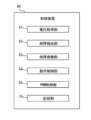
- FIG. 2 is a diagram showing a configuration example of a control device in the power conversion system shown in FIG. 1.
- FIG. 3 is a diagram showing an example of a short circuit failure detection operation of a control device in the power conversion system shown in FIGS. 1 and 2.
- FIG. 4 is a diagram illustrating the operating principle of short circuit failure detection operation of the control device in the power conversion system shown in FIGS. 1 to 3.
- FIG. It is a figure showing the example of composition of the power converter concerning the modification of a 1st embodiment. It is a figure showing the example of composition of the power conversion system concerning a 2nd embodiment.
- FIG. 2 is a diagram illustrating a configuration example of a power conversion system according to a comparative example.
- FIG. 1 is a diagram showing a configuration example of a power conversion system 1 according to a first embodiment.
- the power conversion system 1 includes a DC power source (solar cell) 10, an AC power system (system) 20, a power converter 30, a coil 40, a voltage detection circuit 50, and a control device 60. has.
- a power conversion system (PCS: Power Conditioning Subsystem) 1, for example, converts DC power supplied from a DC power supply 10 into AC power via a power converter 30, and supplies the converted AC power to an AC power system 20. Output to.
- PCS Power Conditioning Subsystem
- the DC power supply 10 is connected to one end of the power converter 30 via the wiring 11, and supplies DC power to the power converter 30 via the one end.
- the DC power supply 10 may be, for example, a solar cell (PV: Photovoltaics), a storage battery (ESS: Energy Storage System), or a DC power supply system consisting of a wind power generator, an AC/DC converter, etc. Further, the DC power supply 10 may be, for example, a capacitor, a system, an input/output section of another power converter, or the like.
- a “solar cell 10" will be explained as an example of the DC power supply 10. Note that the DC power source (solar cell) 10 is an example of a "power source or a capacitor.”
- the wiring 11 is a conductor (DC conductor) that connects the solar cell 10 and one end of the power converter 30.
- the wiring 11 on the positive electrode P side is also referred to as the "positive electrode wiring 11P”
- the wiring 11 on the negative electrode N side is also referred to as the "negative electrode wiring 11N.”
- the wiring 11 is, for example, an electric wire, a bus bar, a printed circuit board wiring, or the like.
- the wiring 11 has a parasitic inductance (self-inductance) L1 . Note that in FIG. 1, the parasitic inductance (self-inductance) L 1 (and magnetic flux ⁇ , which will be described later) is concentrated in a part of the wiring 11 for convenience, but in reality it exists in the entire wiring 11. There is.
- the AC power system 20 (hereinafter also referred to as "system 20") is connected to the output end, which is the other end of the power converter 30, via the AC circuit 21.
- the grid 20 is a system that integrates power generation, transformation, power transmission, and distribution for supplying AC power output from the power converter 30 to power receiving equipment of consumers. ing. Note that the AC power system (system) 20 is an example of a "power supply or capacitor”.
- the AC circuit 21 is, for example, a three-phase three-wire three-phase AC circuit that supplies three-phase AC power, which is a combination of three systems of single-phase AC in which the phases of current or voltage are shifted from each other, using three wires 22. be.
- the wiring 22 is a conductor such as an electric wire or cable in the AC circuit 21, and like the wiring 11, it may be, for example, an electric wire, a bus bar, a printed circuit board wiring, or the like.
- the U-phase, V-phase, and W-phase wiring 22 in the AC circuit 21 are also referred to as "U-phase wiring 22U,” “V-phase wiring 22V,” and “W-phase wiring 22W,” respectively. be done.
- the power converter 30 is connected at one end on the left side in FIG. 1 to the solar cell 10 via wiring 11, and at the other end on the right side in FIG. 20. Further, the power converter 30 is connected to a control device 60 via a signal line (not shown) or the like, and its operation is controlled by the control device 60. The power converter 30 converts the DC power supplied from the solar cell 10 into AC power and outputs it to the grid 20 under the control of the control device 60 .
- the power converter 30 is not limited to one that converts DC power to AC power, and may be one that converts DC power to DC power or one that converts AC power to AC power. .
- what is connected to one end of the power converter 30 is not limited to the DC power source (solar cell) 10, but may be an AC power source.
- the power converter 30 may convert either active power or reactive power, or both.
- the power converter 30 may be connected to a "power source or a capacitor" on the DC side, the AC side, or both the AC side and the DC side.
- the power converter 30 includes a DC capacitor 31, an inverter circuit 32, and an AC reactor 33.
- the DC capacitor 31 is a capacitor for smoothing fluctuations in voltage between terminals, and is connected between the positive electrode wiring 11P and the negative electrode wiring 11N in the wiring 11. Note that the DC capacitor 31 is an example of a "power supply or capacitor”.
- the inverter circuit 32 is constructed of, for example, a plurality of semiconductor switching elements Q such as IGBTs (Insulated Gate Bipolar Transistors). Note that the semiconductor switching element Q is not limited to this, and may be a MOSFET (metal-oxide-semiconductor field-effect transistor) or the like.
- the inverter circuit 32 has one end connected to the solar cell 10 and the other end, which is the output side, connected to the grid 20 via the AC reactor 33.
- the inverter circuit 32 uses a pulse width modulation (PWM) signal, which is a gate drive signal (gate signal) for the semiconductor switching element Q, generated by a PWM control section 65 (see FIG. 2), which will be described later, in the control device 60. controlled.
- PWM pulse width modulation
- the inverter circuit 32 acquires DC power supplied from the solar cell 10 from one end, converts the acquired DC power into AC power under control by a PWM signal (gate signal), and converts the acquired DC power into AC power from the other end which is the output end. and supplies it to the system 20.
- PWM pulse width modulation
- the inverter circuit 32 has, for example, a circuit in which three legs (U-phase leg, V-phase leg, and W-phase leg) are connected in parallel.
- Each leg is configured by, for example, two arms each having a semiconductor switching element Q and a freewheeling diode D connected in antiparallel to each other and connected in series.
- Each leg is connected in parallel, for example, between the positive electrode wiring 11P and the negative electrode wiring 11N, and the midpoint of each leg is connected to the U-phase wiring 22U, V-phase wiring 22V, and W-phase wiring 22W of the AC circuit 21, respectively. electrically connected.
- the AC reactor 33 is also called an AC (alternating-current) reactor, and is connected in series to the AC circuit 21 on the output side of the inverter circuit 32.
- the AC reactor 33 is, for example, a smoothing element that has the effect of reducing noise and suppressing surge voltage.
- the AC reactor 33 constitutes an LC filter circuit (filter circuit) that reduces ripples (vibrations) generated when the semiconductor switching element Q of the inverter circuit 32 switches, together with an AC capacitor (not shown) connected in an L-shape. do.
- the coil 40 is arranged around the wiring 11. For example, if a short-circuit failure occurs in some of the semiconductor switching elements Q of the inverter circuit 32, the circuit voltage of the DC capacitor 31 is applied to the parasitic inductance L1 of the wiring 11, and a magnetic flux ⁇ is generated around it. Therefore, the coil 40 is arranged around the wiring 11 at a position where the magnetic flux ⁇ interlinks with the coil 40 so as to detect the magnetic flux ⁇ .
- L2 is the self-inductance of the coil 40. Note that the positional relationship between the wiring 11 and the coil 40 shown in FIG. It is not limited to the location where it can be used. As mentioned above, in FIG.
- the parasitic inductance (self-inductance) L1 and magnetic flux ⁇ of the wiring 11 are shown concentrated in a part of the wiring 11 for convenience, but in reality, they are shown in the entire wiring 11. Existing.
- the self-inductance L2 of the coil 40 is described concentratedly on a part of the coil 40 for convenience, but in reality it exists throughout the entire coil 40.
- the coil 40 is composed of, for example, electric wires, busbars, printed circuit board wiring, and the like.
- the coil 40 may be of any type as long as it can detect the magnetic flux ⁇ generated when a short-circuit failure occurs, and may be, for example, a coil of general electric wire wound several times.
- the coil 40 is electrically insulated from the main circuit (for example, the wiring 11) including the power converter 30, and is not subjected to a large voltage unlike the main circuit. Therefore, compared to a case where the coil 40 is not insulated from the main circuit, the insulation performance does not need to be high, and the insulation distance does not need to be large. Note that both ends of the coil 40 are connected to the voltage detection circuit 50.
- the voltage detection circuit 50 is connected to both ends of the coil 40 and constantly detects the voltage value V of the voltage across the coil 40. Note that the voltage detection circuit 50 may detect the voltage value V of the voltage across the coil 40, for example, at predetermined time intervals, and may detect the voltage value V of the voltage across the coil 40 at predetermined time intervals. Detection may be performed according to the instructions provided. Note that the voltage detection circuit 50 may be built into the power converter 30 or the control device 60, or may be built into an external device or host device (not shown).
- the control device 60 is provided, for example, inside or outside the power converter 30, and although wiring etc. are omitted in the figure, each element of the power converter 30 including the inverter circuit 32, and the voltage detection circuit 50 and are electrically connected by wire or wirelessly. Note that the control device 60 may be implemented as a function of an inverter control circuit (not shown).
- the control device 60 includes a processor 91 (see FIG. 10), which will be described later, such as a CPU (Central Processing Unit), MPU (Micro Processing Unit), or GPU (Graphics Processing Unit) that operates by executing a program, for example.
- the control device 60 includes a storage section 70 (see FIG. 2), a memory 92 (see FIG. 10), etc., which will be described later. is operated to collectively control the operation of the power converter 30.
- the control device 60 may operate according to instructions received from an operator or the like via a host device (not shown) or an operation unit (not shown), for example.
- the control device 60 detects a short-circuit failure in the semiconductor switching element Q or the like according to the magnitude of the voltage value V of the voltage across the coil 40 detected by the voltage detection circuit 50.
- FIG. 2 is a diagram showing a configuration example of the control device 60 in the power conversion system 1 shown in FIG. 1.
- the control device 60 has a storage unit 70, and functions as the following units by, for example, executing a predetermined program stored in the storage unit 70 or a memory 92 (see FIG. 10) described below. That is, the control device 60 functions as a voltage acquisition section 61, a failure detection section 62, a failure reporting section 63, an operation control section 64, and a PWM control section 65 by executing a predetermined program. Note that each of the above functions may be realized by a program executed by the processor 91 (see FIG. 10) included in the control device 60, or may be realized by the hardware 93 (see FIG. 10). Each of the above units executes a predetermined program to perform the following processing.
- the voltage acquisition unit 61 is connected to the voltage detection circuit 50 and constantly acquires the voltage value V of the voltage across the coil 40 detected by the voltage detection circuit 50. Note that the voltage acquisition unit 61 may acquire the voltage value V of the voltage across the coil 40 at predetermined time intervals, for example, and may receive the voltage value V of the voltage across the coil 40 from an operator or the like via a host device (not shown) or an operation unit (not shown). You may obtain it by following the instructions provided.
- the failure detection unit 62 detects a short circuit failure in the semiconductor switching element Q, etc., depending on the magnitude of the voltage value V of the voltage across the coil 40 acquired by the voltage acquisition unit 61. For example, the failure detection unit 62 compares the voltage value V of the voltage across the coil 40 acquired by the voltage acquisition unit 61 with a predetermined threshold value stored in the storage unit 70 or a memory 92 (see FIG. 10) to be described later. do. For example, when the voltage value V is larger than a predetermined threshold value, the failure detection unit 62 detects a short circuit failure in the semiconductor switching element Q or the like.
- the failure detection unit 62 calculates a predetermined judgment value based on current conditions, simulation results, etc., and compares the calculated predetermined judgment value with the voltage value V of the voltage across the coil 40. A short circuit fault may also be detected.
- the failure detection unit 62 detects a short circuit failure, it outputs information to the effect that a short circuit failure has been detected to at least one of the failure reporting unit 63 and the operation control unit 64.
- the failure reporting unit 63 When the failure reporting unit 63 acquires information indicating that a short circuit failure has been detected from the failure detection unit 62, it issues failure information.
- the failure reporting unit 63 detects a failure by, for example, outputting failure information to a host device (not shown) or displaying a warning or an alarm on a display unit (not shown) or an operation unit (not shown) of the power converter 30. Report information. Note that the failure reporting unit 63 may report failure information to the operation control unit 64.
- the operation control unit 64 When the operation control unit 64 acquires information indicating that a short-circuit failure has been detected from the failure detection unit 62 or receives notification of failure information from the failure notification unit 63, the operation control unit 64 controls the power converter 30. An operation instruction is given to each part of the power converter 30 to stop the protection.
- the operation control unit 64 may, for example, give an operation instruction to the PWM control unit 65 to protectively stop (gate block) the switching operation of the semiconductor switching element Q, thereby causing the power converter 30 to be protectively stopped. Further, the operation control unit 64 may protect the power converter 30 by, for example, performing a protective operation such as opening a circuit breaker (switch), etc. (not shown) of the power converter 30.
- the operation control unit 64 performs a protective operation such as opening a circuit breaker (switch) (not shown) between the other power converter 30 or the solar cell 10 connected in parallel, for example. The expansion of failures in the power conversion system 1 may be prevented.
- the operation control unit 64 may issue an operation instruction to stop the power converter 30 for protection, for example, in accordance with an instruction received from an operator or the like via a host device (not shown) or an operation unit (not shown).
- control device 60 may have the function of either the failure reporting section 63 or the operation control section 64, and these functions are not provided in an external device such as a host device (not shown). There may be.
- the PWM control unit 65 performs PWM control based on, for example, a predetermined output voltage command signal and a predetermined triangular wave carrier signal, and generates a gate signal that turns on and off the semiconductor switching element Q of the inverter circuit 32.
- the PWM control unit 65 outputs the generated gate signal to the inverter circuit 32 of the power converter 30 and controls the operation of the inverter circuit 32.
- the PWM control unit 65 receives an operation instruction to stop the power converter 30 from a protective stop from the operation control unit 64, the PWM control unit 65 controls the operation of the inverter circuit 32 to stop the operation of the semiconductor switching element Q.
- the power converter 30 is brought to a protective stop.
- the storage unit 70 is, for example, a volatile or nonvolatile storage medium such as an HDD (Hard Disk Drive), an SSD (Solid State Drive), a DRAM (Dynamic Random Access Memory), or other semiconductor memory.
- the storage unit 70 stores, for example, programs necessary for the operation of each part of the control device 60, and various information is written and read by each part of the control device 60.
- the storage unit 70 stores the voltage value V of the voltage across the coil 40 acquired by the voltage acquisition unit 61, a predetermined threshold value used for failure detection by the failure detection unit 62, and the like.
- the storage unit 70 is connected to each part of the control device 60 by, for example, a bus (not shown). Note that the storage unit 70 may be provided outside the control device 60 and connected to the control device 60 by wire or wirelessly, or may be an external storage medium such as a memory card or a DVD (Digital Versatile Disc). , online storage, etc. Further, the storage unit 70 may be common to a memory 92 (see FIG. 10), which will be described later.
- FIG. 3 is a diagram showing an example of a short circuit failure detection operation of the control device 60 in the power conversion system 1 shown in FIGS. 1 and 2.
- the short circuit current I1 of the loop may be one that passes through a DC voltage source such as the solar cell 10.
- the coil 40 is arranged around the circuit wiring 11 (electric wire, bus bar, printed circuit board wiring, etc.) so that the magnetic flux ⁇ generated by the short circuit fault intersects with the circuit wiring 11 (electric wire, bus bar, printed circuit board wiring, etc.). ing. Then, the voltage value V of the voltage across the coil 40 is detected by the voltage detection circuit 50. In this case, the voltage acquisition unit 61 of the control device 60 acquires the voltage value V of the voltage across the coil 40 detected by the voltage detection circuit 50. Then, the failure detection unit 62 of the control device 60 compares the voltage value V with a predetermined threshold value, and detects a short circuit failure when the voltage value V exceeds the predetermined threshold value.
- the failure reporting unit 63 of the control device 60 acquires information indicating that a short-circuit failure has been detected, the failure reporting unit 63 of the control device 60 issues failure information, and the operation control unit 64 of the control device 60 protects the power converter 30.
- An operation instruction is given to each part of the power converter 30 to stop it.
- the PWM control unit 65 of the control device 60 controls the operation of the inverter circuit 32 to put the power converter 30 into a protective stop. Thereby, the power conversion system 1 can be protected and furthermore, failure can be prevented from expanding.
- the DC capacitor 31 is connected to the power converter 30 and the short circuit of the voltage charged in the DC capacitor 31 is detected to protect the power conversion system 1 and prevent the spread of failure.
- the present invention is not limited to this, and even if a power source such as a solar cell, a storage battery, or a grid is connected to the power converter 30 and the voltage of the power source is short-circuited, the power conversion system 1 can be operated in the same manner as described above. It is possible to protect the device and prevent the spread of failure.
- the coil 40 may be arranged around the wiring 22 so that the magnetic flux ⁇ generated by the short-circuit failure interlinks with the coil 40 .
- the coil 40 may be placed at position A in FIG.
- FIG. 4 is a diagram illustrating the operating principle of the short circuit failure detection operation of the control device 60 in the power conversion system 1 shown in FIGS. 1 to 3.
- FIG. 4(a) is a diagram showing an equivalent circuit when a short circuit failure occurs in the power conversion system 1 shown in FIGS. 1 to 3.
- FIG. 4(b) is a diagram showing a voltage change that occurs when a short-circuit failure occurs in the equivalent circuit of FIG. 4(a).
- FIG. 4(c) is a diagram showing a current change that occurs in the equivalent circuit of FIG. 4(a) at the time of a short-circuit failure.
- the wiring referred to here is constituted by, for example, electric wires, busbars, printed circuit board wiring, and the like.
- the impedance of the capacitor and the short-circuit point is sufficiently small, most of the voltage of the capacitor is shared by the parasitic inductance (self-inductance) of the wiring, and magnetic flux is generated around the wiring.
- the coils are arranged so that the above magnetic fluxes interlink with each other.
- the coil is composed of, for example, electric wires, busbars, printed circuit board wiring, and the like.
- the parasitic inductance (self-inductance) of the wiring is L1
- the self-inductance of the coil is L2
- the degree of coupling between the parasitic inductance L1 of the wiring and the self-inductance L2 of the coil is k
- the load resistance of the coil is If R, then the equivalent circuit shown in FIG. 4(a) can be drawn.
- Coupled degree k is also called “coupling coefficient k”, and is the magnetic flux between two windings (in the case of Fig. 4 (a), between the short circuit loop on the left and the coil on the right). represents the degree of bonding.
- the degree of coupling k is expressed between 0 and 1. For example, when the degree of coupling k is 1, the magnetic flux generated in one winding completely passes through the other winding without leaking (interlinking). ) represents a relationship. On the other hand, for example, when the degree of coupling k is 0, it represents a relationship in which the magnetic flux generated in one winding does not penetrate (does not interlink) with the other winding at all. Therefore, "magnetic flux generated by a short circuit interlinks” means that the degree of coupling k is greater than 0 (between 0 and 1), and it is preferable that the degree of coupling k is close to 1. .
- the mutual inductance M between the parasitic inductance L1 of the wiring and the self-inductance L2 of the coil is set as shown in the following equation (1).
- i 1 is the current of the parasitic inductance L 1 of the wiring
- i 2 is the current of the self-inductance L 2 of the coil
- s is the Laplace operator
- v 1 corresponds to the voltage divided by the parasitic inductance L 1 of the wiring in the capacitor voltage
- v 2 is the voltage applied to the load resistance R of the coil.
- equation (3) a relational expression between the voltages on the primary side and the secondary side
- v 2 is a first-order delayed response of v 1 , and the time constant is as shown in equation (4) below.
- v 2 is approximately proportional to v 1 .
- the time constant of the first-order lag system is the coefficient of s in equation (3), so if this is small, the time constant of the first-order lag system becomes small. It can be said that v 2 is approximately proportional to v 1 . Therefore, by measuring the voltage across the coil with a voltage detection circuit having a sufficiently large input impedance, it is possible to detect a voltage that is approximately proportional to the voltage of the shorted capacitor when a short circuit accident occurs.
- FIG. 4(b) is a diagram showing voltage changes that occur when a short-circuit failure occurs in the equivalent circuit of FIG. 4(a), where the vertical axis represents voltage and the horizontal axis represents time.
- FIG. 4(c) is a diagram showing a current change that occurs when a short-circuit failure occurs in the equivalent circuit of FIG. 4(a), where the vertical axis represents current and the horizontal axis represents time.
- the horizontal dashed line indicates a predetermined threshold for detecting a short circuit fault. Note that in FIGS. 4(b) and 4(c), the secondary side circuit is temporarily ignored.
- the current i 1 is the reciprocal of the parasitic inductance L 1 of the circuit loop formed by the short circuit, and the time of the short-circuited voltage v 1 , as shown in FIG. 4(c). Approximately proportional to the product of integrals. Therefore, for example, there is a delay in the change in current i 1 shown in FIG. 4(c) with respect to the voltage change that occurs during a short circuit shown in FIG. 4(b).
- the voltage v1 is applied to the parasitic inductance L1 in a stepwise manner as shown in FIG. 4(b).
- the time constant of the first-order lag can be made considerably small, so that a voltage proportional to a substantially unchanged waveform can be detected without delay.
- the current i 1 is an integral of this voltage v 1 , a delay occurs in principle as shown in FIG. 4(c).
- the method of detecting the voltage change that occurs during a short circuit as shown in FIG. 4(b) is more effective than the method of detecting the current change shown in FIG. can be detected at high speed in principle.
- the control device 60 in the power conversion system 1 shown in FIGS. 1 to 3 acquires the voltage value V of the voltage across the coil 40 detected by the voltage detection circuit 50, and By comparing the threshold value, a short circuit fault can be detected without delay.
- the control device detects a short circuit failure in the power converter 30 and takes measures such as stopping the protection of the power converter 30 or opening a circuit breaker (not shown). Perform protective operation.
- the current i 1 generated at the time of a short circuit failure is the reciprocal of the parasitic inductance L 1 of the circuit loop configured by the short circuit, and It is approximately proportional to the time integral product of the short-circuited voltage v1 . Therefore, there is a delay in the current i 1 with respect to the voltage change that occurs at the time of a short circuit.
- short-circuit failures can be detected faster in principle than in the method of detecting short-circuit current I1.
- the coil 40 for detecting the magnetic flux ⁇ generated at the time of a short-circuit failure can also be created by winding a general electric wire several times.
- the coil 40 for detecting the magnetic flux ⁇ generated at the time of a short circuit failure is electrically insulated from the main circuit including the power converter 30. . Therefore, according to the first embodiment shown in FIGS. 1 to 4, the power conversion system 1 can be protected with a simpler and cheaper configuration than in the case of directly measuring and detecting the voltage change that occurs at the time of a short circuit failure. In addition, the expansion of failures in the power conversion system 1 can be prevented.
- the coil 40 for detecting the magnetic flux ⁇ generated at the time of a short-circuit failure can be created by winding a general electric wire several times, and It is electrically insulated from the main circuit including the device 30. Therefore, according to the first embodiment shown in FIGS. 1 to 4, the coil 40 can be retrofitted to the existing power conversion system 1, and the existing power conversion system 1 can be protected by retrofitting. is also possible.
- FIG. 5 is a diagram showing a configuration example of a power converter 30A according to a modification of the first embodiment.
- the same or similar configurations as those in the embodiment shown in FIGS. 1 to 4 are denoted by the same reference numerals, and detailed description thereof will be omitted or simplified. Note that, in FIG. 5, for the sake of simplicity, some components that are the same or similar to those of the embodiments shown in FIGS. 1 to 4 are omitted or simplified.
- the power converter 30A shown in FIG. 5 has almost the same configuration as the power converter 30 shown in FIG. 1, but some components have been changed.
- the power converter 30A two DC capacitors 31 are arranged in parallel, three semiconductor modules forming an inverter circuit 32 are arranged, and these are connected by a bus bar forming a wiring 11.
- a loop short-circuit current I3 flows from the DC capacitor 31 toward the short-circuit point of this semiconductor module. Since a magnetic flux ⁇ is generated where there is a current loop, in the embodiment shown in FIG. 5, a coil 40 is placed above the loop of the short-circuit current I3 so that the magnetic flux ⁇ can be picked up.
- the coil 40 is connected to the parasitic inductance L1.
- the voltage applied to L1 is also picked up.
- the coil 40 may be placed anywhere as long as it is interlinked with the magnetic flux ⁇ generated by the loop of the short-circuit current I3.
- the coil 40 may be placed at a location indicated by B in FIG. 5.
- the installation position of the coil 40 is not easily known, such as when the magnetic flux ⁇ generated by the loop of the short circuit current I3 is interlinked, based on the laws of electromagnetism, the magnetic flux generated around the short circuit current I3 can be The direction and size may be roughly estimated, and the coil 40 may be arranged so that a sufficiently large magnetic flux is interlinked with the coil 40.
- the magnetic flux generated around the loop of the short-circuit current I3 may be calculated by numerical analysis using a computer, and the coil 40 may be arranged so that a sufficiently large magnetic flux is interlinked with the coil 40.
- the coil 40 may be placed above the loop of the short-circuit current I4, for example at the position C in FIG. 5, so that the magnetic flux ⁇ of the loop of the short-circuit current I4 can be picked up.
- FIG. 6 is a diagram showing a configuration example of a power conversion system 1B according to the second embodiment.
- the same or similar configurations as those in the embodiment shown in FIGS. 1 to 5 are denoted by the same reference numerals, and detailed description thereof will be omitted or simplified.
- the wiring 11 connected to the upper power converter 30B is branched at the connection point P1, and is connected to the wiring 13 connected to the lower power converter 30B by the vertical wiring 12 in FIG. There is.
- the vertical wiring 12 is a wiring that connects the upper power converter 30B and the lower power converter 30B.
- a loop short-circuit current I5 flows from the DC capacitor 31 of the upper power converter 30B.
- a loop short-circuit current I6 also flows from the DC capacitor 31 of the lower power converter 30B.
- the coil 40 is placed at a position where the short circuit current I5 of the loop flows. That is, in the embodiment shown in FIGS. 1 to 4, the coil 40 is arranged at a position where the voltage applied to the parasitic inductance L1 between the DC capacitor 31 and the semiconductor switching element Q in the upper power converter 30B can be detected.
- the coil 40 is arranged at a position where the voltage applied to the parasitic inductance L1 between the DC capacitor 31 and the semiconductor switching element Q in the upper power converter 30B can be detected.
- the coil 40 is arranged at a position where the magnetic flux ⁇ generated by the short circuit fault intersects. That is, in the embodiment shown in FIG. 6, since the loop short circuit current I6 flows, the coil 40 is arranged around the vertical wiring 12 so as to pick up the magnetic flux ⁇ along the path of the short circuit current I6. In other words, the coil 40 is placed at a position on the wiring 12 where it can pick up the voltage applied to the parasitic inductance L1 between the two parallel-connected power converters 30B.
- the voltage can be detected even if a short-circuit failure occurs in either of the two power converters 30B connected in parallel. Furthermore, if the coil 40 is placed at the position of the wiring 12 that connects the power converters 30B, even if two or more power converters 30B are connected in parallel, which one of the power Even if a short circuit failure occurs in converter 30B, coil 40 can detect voltage.
- the coil 40 may be placed around the vertical wiring 23 on the AC side at a position where the magnetic flux ⁇ generated due to a short circuit intersects.
- the coil 40 may be placed at position D in FIG.
- the coil 40 is located around the wiring 12 that connects the plurality of power converters 30B, and the magnetic flux ⁇ generated due to the short-circuit failure interlinks with the coil 40. placed in position.
- the second embodiment shown in FIG. 6 it is possible to suppress the number of coils 40, and it is possible to protect the power conversion system 1B with a simpler and cheaper configuration. It is possible to prevent the failure from expanding in the conversion system 1B.
- FIG. 7 is a diagram showing a configuration example of a power converter 30C according to a modification of the second embodiment.
- the same or similar configurations as those in the embodiment shown in FIGS. 1 to 6 are denoted by the same reference numerals, and detailed description thereof will be omitted or simplified. Note that, in FIG. 7, for the sake of simplicity, some components that are the same or similar to those of the embodiments shown in FIGS. 1 to 6 are omitted or simplified.
- the power converter 30C shown in FIG. 7 has almost the same configuration as the power converter 30B shown in FIG. 6, but some components are changed.
- two DC capacitors 31 are arranged, and three semiconductor modules forming an inverter circuit 32 are arranged.
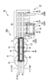
- These DC capacitors 31 and the semiconductor module (inverter circuit) 32 are connected by a busbar 14 that constitutes the wiring 14 in the upper power converter 30C, and are connected by a busbar 14 that constitutes the wiring 13 in the lower power converter 30C. It is connected by 13.
- the busbar 14 in the upper power converter 30C and the busbar 13 in the lower power converter 30C are connected by the busbar 12 that constitutes the vertical wiring 12. Further, the vertical bus bar 12 is connected to the solar cell 10 by the bus bar 11 that constitutes the wiring 11.
- short-circuit failure occurs around the vertical bus bar 12 that connects the upper power converter 30C and the lower power converter 30C (between the power converters 30C).
- the coil 40 is arranged at a position where the magnetic flux ⁇ generated by the above interlinks with each other. That is, in the embodiment shown in FIG. 7, since the loop short-circuit current I7 flows, the coil 40 is arranged around the vertical bus bar 12 so as to pick up the magnetic flux ⁇ along the path of the short-circuit current I7. In other words, the coil 40 is placed at a position on the busbar 12 where it can pick up the voltage applied to the parasitic inductance L1 between the two parallel-connected power converters 30C.
- FIG. 8 is a diagram showing a configuration example of a power converter 30D according to the third embodiment.
- the same or similar configurations as those in the embodiment shown in FIGS. 1 to 7 are denoted by the same reference numerals, and detailed description thereof will be omitted or simplified. Note that, in FIG. 8, for the sake of simplicity, some components that are the same or similar to those of the embodiments shown in FIGS. 1 to 7 are omitted or simplified.
- the power converter 30D has a neutral point clamp type three-level inverter circuit 32D.
- a loop short circuit current I8 a loop short circuit current I9, etc. flow from the DC capacitor 31.
- the coil 40 is arranged to cover the entire vertical wiring 15 in FIG. 8, which connects the positive wiring 11P, the neutral wiring 11M, and the negative wiring 11N. Accordingly, in the embodiment shown in FIG. 8, the coil 40 can pick up the magnetic flux ⁇ of either path of the loop short-circuit current I8 and the loop short-circuit current I9 (interlinks with the magnetic flux ⁇ of either path). . Further, by arranging the coil 40 at the position shown in FIG. 8, the short circuit fault can be detected even if the short circuit fault occurs in any of the semiconductor switching elements Q of the inverter circuit 32D.
- FIG. 9 is a diagram showing a configuration example of a power converter 30E according to the fourth embodiment.
- the same or similar configurations as those in the embodiment shown in FIGS. 1 to 8 are denoted by the same reference numerals, and detailed description thereof will be omitted or simplified. Note that, in FIG. 9, for the sake of simplicity, some components that are the same or similar to those of the embodiments shown in FIGS. 1 to 8 are omitted or simplified.
- the power converter 30E has a neutral point switch type three-level inverter circuit 32E.
- the coil 40 is arranged to cover the entire vertical wiring 15 in FIG. 9, which connects the positive wiring 11P, the neutral wiring 11M, and the negative wiring 11N.
- the coil 40 can pick up the magnetic flux ⁇ of either path of the loop short-circuit current I10 and the loop short-circuit current I11 (interlinks with the magnetic flux ⁇ of either path).
- the short circuit fault can be detected even if the short circuit fault occurs in any of the semiconductor switching elements Q of the inverter circuit 32E.
- FIG. 10 is a conceptual diagram showing an example of the hardware configuration of a processing circuit included in the control device 60 in the embodiments shown in FIGS. 1 to 9.
- the processing circuit includes at least one processor 91 and at least one memory 92.
- the processing circuitry includes at least one dedicated hardware 93.
- each function is realized by software, firmware, or a combination of software and firmware. At least one of the software and firmware is written as a program. At least one of software and firmware is stored in memory 92.
- the processor 91 implements each function by reading and executing programs stored in the memory 92.
- the processing circuitry comprises dedicated hardware 93
- the processing circuitry may be, for example, a single circuit, a composite circuit, a programmed processor, or a combination thereof. Each function is realized by a processing circuit.
- Each function of the control device 60 may be partially or entirely configured by hardware, or may be configured as a program executed by a processor. That is, the control device 60 can be realized by a computer and a program, and the program can be stored in a storage medium or provided through a network.
- FIG. 11 is a diagram illustrating a configuration example of a power conversion system 100 according to a comparative example.
- the same or similar configurations as those in the embodiment shown in FIGS. 1 to 10 are denoted by the same reference numerals, and detailed description thereof will be omitted or simplified.
- a plurality of unit power converters 130 are connected in parallel.
- the plurality of unit power converters 130 have their DC sides connected to a DC power supply 110 (not shown), and their AC sides connected to the system 120.
- Each of the plurality of unit power converters 130 includes an inverter circuit 132, a DC capacitor 131, and an AC reactor 133, and the inverter circuit 132 includes a plurality of switching elements (not shown).
- the positive electrode P side and the negative electrode N side are connected to each other, and the neutral points M are not connected to each other. Furthermore, in the plurality of unit power converters 130, a current sensor 134 is provided on the positive electrode P side, and detects the current flowing to the positive electrode P side. Note that the current sensor 134 may be provided on the negative electrode N side to detect the current flowing to the negative electrode N side.
- the current sensor 134 must be placed in each of the plurality of unit power converters 130.
- electric wires and voltage sensors must be placed in each of the plurality of unit power converters 130. For this reason, it is necessary to arrange as many current sensors 134 and electric wires and voltage sensors (not shown) as there are unit power converters 130, which may result in high costs.
- the coil 40 is arranged around the wiring 11 and the like at a position where the magnetic flux ⁇ generated due to a short circuit fault interlinks, and the voltage detection circuit 50 detects the coil 40.
- a short circuit failure is detected by detecting the voltage value V of the voltage across the terminal.
- the coil 40 for detecting the magnetic flux ⁇ generated at the time of a short-circuit failure can also be created by winding a general electric wire several times. Therefore, according to the embodiment shown in FIGS. 1 to 10, the power conversion system 1 and the like can be protected with a simpler and cheaper configuration than the comparative example shown in FIG. 11.
- short-circuit failures can be detected faster in principle than the method of detecting short-circuit current I' in the comparative example shown in FIG.
- the coil 40 for detecting the magnetic flux ⁇ generated at the time of a short-circuit failure is electrically insulated from the main circuit. Therefore, according to the embodiments shown in FIGS. 1 to 10, the power conversion system 1 etc. can be protected with a simpler and cheaper configuration than the method of directly measuring the voltage value V' in the comparative example shown in FIG. can do.
- the coil 40 can be installed as an afterthought, and the existing power conversion system 1 etc. can be protected as an afterthought. It is also possible.
- FIGS. 1 to 10 unlike the comparative example shown in FIG. 11, even when a plurality of power converters 30 are connected in parallel, one coil 40 is arranged. If so, the short-circuit failure can be detected even if the short-circuit failure occurs in any of the power converters 30. Therefore, according to the embodiment shown in FIGS. 1 to 10, the power conversion system 1 and the like can be protected with a simpler and cheaper configuration than the comparative example shown in FIG. 11.
- the power conversion systems 1 to 1E power converters 30 to 30E
- the control device 60 they have have been described as an example of one aspect of the present disclosure. It is not limited to this.
- the present disclosure can also be realized as a short circuit failure detection method in which processing steps are performed in each part of the control device 60.
- the present disclosure can also be realized as a short circuit failure detection program that causes a computer to execute processing steps in each part of the control device 60.
- the present disclosure can also be realized as a storage medium (non-temporary computer readable medium) in which a short circuit failure detection program is stored.
- the short circuit fault detection program can be stored and distributed on a removable disk such as a CD (Compact Disc), DVD (Digital Versatile Disc), or USB (Universal Serial Bus) memory, for example.
- the short circuit failure detection program may be uploaded onto the network via a network interface (not shown) included in the control device 60, or may be downloaded from the network and stored in the storage unit 70 or the like.
- Inverter circuit semiconductor module
Landscapes
- Engineering & Computer Science (AREA)
- Power Engineering (AREA)
- Inverter Devices (AREA)
Abstract
Description
図1は、第1実施形態に係る電力変換システム1の構成例を示す図である。
図3は、図1及び図2に示す電力変換システム1における制御装置60の短絡故障検出動作の一例を示す図である。
図4は、図1から図3に示す電力変換システム1における制御装置60の短絡故障検出動作の動作原理を説明する図である。図4(a)は、図1から図3に示す電力変換システム1に短絡故障が発生したときの等価回路を示す図である。図4(b)は、図4(a)の等価回路において短絡故障時に生じる電圧変化を示す図である。図4(c)は、図4(a)の等価回路において短絡故障時に生じる電流変化を示す図である。




以上、図1から図4に示す第1実施形態では、太陽電池10、直流コンデンサ31、系統20等の電源の電圧が短絡される短絡故障が発生したときに、配線11や配線22の周囲であって、短絡故障によって発生する磁束Φが鎖交する位置にコイル40が配置される。そして、電圧検出回路50によってコイル40の両端電圧の電圧値Vが検出され、検出されたコイル40の両端電圧の電圧値Vが制御装置60によって取得される。そして、制御装置は、取得された電圧値Vが所定の閾値を超えるときに、電力変換器30の短絡故障を検出し、電力変換器30の保護停止や、不図示の遮断器の開放などの保護動作を行う。これにより、図1から図4に示す第1実施形態によれば、従来よりも簡素で安価な構成で、電力変換システム1を保護することができ、また、電力変換システム1の故障拡大を防ぐことができる。
図5は、第1実施形態の変形例に係る電力変換器30Aの構成例を示す図である。なお、図5に示す実施形態では、図1~図4に示す実施形態と同一又は同様の構成については同一の符号を付し、詳細な説明は省略又は簡略化する。なお、図5においては、図面の簡単のため、図1~図4に示す実施形態と同一又は同様の一部構成要素については、省略又は簡略化して示されている。
図6は、第2実施形態に係る電力変換システム1Bの構成例を示す図である。なお、図6に示す実施形態では、図1~図5に示す実施形態と同一又は同様の構成については同一の符号を付し、詳細な説明は省略又は簡略化する。
図7は、第2実施形態の変形例に係る電力変換器30Cの構成例を示す図である。なお、図7に示す実施形態では、図1~図6に示す実施形態と同一又は同様の構成については同一の符号を付し、詳細な説明は省略又は簡略化する。なお、図7においては、図面の簡単のため、図1~図6に示す実施形態と同一又は同様の一部構成要素については、省略又は簡略化して示されている。
図8は、第3実施形態に係る電力変換器30Dの構成例を示す図である。なお、図8に示す実施形態では、図1~図7に示す実施形態と同一又は同様の構成については同一の符号を付し、詳細な説明は省略又は簡略化する。なお、図8においては、図面の簡単のため、図1~図7に示す実施形態と同一又は同様の一部構成要素については、省略又は簡略化して示されている。
図9は、第4実施形態に係る電力変換器30Eの構成例を示す図である。なお、図9に示す実施形態では、図1~図8に示す実施形態と同一又は同様の構成については同一の符号を付し、詳細な説明は省略又は簡略化する。なお、図9においては、図面の簡単のため、図1~図8に示す実施形態と同一又は同様の一部構成要素については、省略又は簡略化して示されている。
図10は、図1~図9に示した実施形態における制御装置60が有する処理回路のハードウェア構成例を示す概念図である。上述した各機能は処理回路により実現される。一態様として、処理回路は、少なくとも1つのプロセッサ91と少なくとも1つのメモリ92とを備える。他の態様として、処理回路は、少なくとも1つの専用のハードウェア93を備える。
図11は、比較例に係る電力変換システム100の構成例を示す図である。なお、図11に示す実施形態では、図1~図10に示す実施形態と同一又は同様の構成については同一の符号を付し、詳細な説明は省略又は簡略化する。
以上、図1から図10に示す実施形態によれば、本件開示の一態様として、電力変換システム1~1E(電力変換器30~30E)及びこれらが有する制御装置60を例に説明したが、これには限られない。本件開示は、制御装置60の各部における処理ステップが行われる短絡故障検出方法としても実現可能である。
Claims (8)
- 電源又はコンデンサと配線を介して接続される電力変換器と、
前記電源又はコンデンサの電圧が短絡される短絡故障が発生したときに、前記配線の周囲であって、前記短絡故障によって発生する磁束が鎖交する位置に配置されるコイルと、
前記コイルの両端電圧の電圧値を検出する電圧検出回路と、
を備える電力変換システムの制御装置であって、
前記電圧検出回路によって検出される前記コイルの両端電圧の前記電圧値を取得する電圧取得部と、
前記電圧取得部によって取得される前記電圧値に基づいて、前記電力変換器の短絡故障を検出する故障検出部と、
を備えることを特徴とする制御装置。 - 請求項1に記載の制御装置において、
前記故障検出部は、前記電圧値が所定の閾値を超えるときは、前記電力変換器の前記短絡故障を検出する
ことを特徴とする制御装置。 - 請求項1又は請求項2に記載の制御装置において、
前記故障検出部によって、前記電力変換器の短絡故障が検出されるときは、前記電力変換器を保護停止させる動作指示を出力する動作制御部をさらに備える
ことを特徴とする制御装置。 - 電源又はコンデンサと配線を介して接続される電力変換器と、
前記電源又はコンデンサの電圧が短絡する短絡故障が発生したときに、前記配線の周囲であって、前記短絡故障によって発生する磁束が鎖交する位置に配置されるコイルと、
前記コイルの両端電圧の電圧値を検出する電圧検出回路と、
請求項1から請求項3のいずれか1項に記載の制御装置と、
を備えることを特徴とする電力変換システム。 - 請求項4に記載の電力変換システムにおいて、
前記配線は、電線、ブスバー、又はプリント基板配線のいずれかである
ことを特徴とする電力変換システム。 - 請求項4又は請求項5に記載の電力変換システムにおいて、
前記コイルは、電線、ブスバー、又はプリント基板配線のいずれかである
ことを特徴とする電力変換システム。 - 請求項4から請求項6の何れか1項に記載の電力変換システムにおいて、
前記コイルは、主回路とは電気的に絶縁されている
ことを特徴とする電力変換システム。 - 請求項4から請求項7の何れか1項に記載の電力変換システムにおいて、
前記電力変換器が、前記電源又はコンデンサと、前記配線を介して複数台並列接続されるときは、前記コイルは、複数台の前記電力変換器同士を接続する前記配線の周囲であって、前記短絡故障によって発生する磁束が鎖交する位置に配置される
ことを特徴とする電力変換システム。
Priority Applications (3)
| Application Number | Priority Date | Filing Date | Title |
|---|---|---|---|
| JP2023564051A JP7540609B2 (ja) | 2022-05-12 | 2022-05-12 | 電力変換システム |
| US18/561,491 US12483157B2 (en) | 2022-05-12 | 2022-05-12 | Power conversion system |
| PCT/JP2022/020055 WO2023218599A1 (ja) | 2022-05-12 | 2022-05-12 | 電力変換システムの制御装置及び電力変換システム |
Applications Claiming Priority (1)
| Application Number | Priority Date | Filing Date | Title |
|---|---|---|---|
| PCT/JP2022/020055 WO2023218599A1 (ja) | 2022-05-12 | 2022-05-12 | 電力変換システムの制御装置及び電力変換システム |
Publications (1)
| Publication Number | Publication Date |
|---|---|
| WO2023218599A1 true WO2023218599A1 (ja) | 2023-11-16 |
Family
ID=88730052
Family Applications (1)
| Application Number | Title | Priority Date | Filing Date |
|---|---|---|---|
| PCT/JP2022/020055 Ceased WO2023218599A1 (ja) | 2022-05-12 | 2022-05-12 | 電力変換システムの制御装置及び電力変換システム |
Country Status (3)
| Country | Link |
|---|---|
| US (1) | US12483157B2 (ja) |
| JP (1) | JP7540609B2 (ja) |
| WO (1) | WO2023218599A1 (ja) |
Citations (5)
| Publication number | Priority date | Publication date | Assignee | Title |
|---|---|---|---|---|
| JPH09205779A (ja) * | 1996-01-25 | 1997-08-05 | Hitachi Ltd | 電力変換装置 |
| US6271655B1 (en) * | 1997-07-24 | 2001-08-07 | Robert Bosch Gmbh | Planar coil device, method and system for sensing changing currents in a planar conductor path |
| JP2003224929A (ja) * | 2002-01-25 | 2003-08-08 | Mitsubishi Electric Corp | 電力変換装置 |
| WO2004077076A1 (de) * | 2003-02-28 | 2004-09-10 | Abb Schweiz Ag | Kurzschlussdetektion in einer umrichterschaltung |
| JP2019106784A (ja) * | 2017-12-12 | 2019-06-27 | 東芝三菱電機産業システム株式会社 | 電力変換装置 |
Family Cites Families (4)
| Publication number | Priority date | Publication date | Assignee | Title |
|---|---|---|---|---|
| JP6559970B2 (ja) * | 2014-11-05 | 2019-08-14 | 三星電子株式会社Samsung Electronics Co.,Ltd. | コンバータ装置、インバータ装置及び交流機駆動装置 |
| JP7294424B2 (ja) | 2019-07-23 | 2023-06-20 | 東芝三菱電機産業システム株式会社 | 多重電力変換システム |
| CN113228492A (zh) * | 2019-07-23 | 2021-08-06 | 东芝三菱电机产业系统株式会社 | 复合电力变换系统 |
| JP7118284B2 (ja) * | 2019-08-30 | 2022-08-15 | 三菱電機株式会社 | 直流電源装置、モータ駆動装置、送風機、圧縮機及び空気調和機 |
-
2022
- 2022-05-12 JP JP2023564051A patent/JP7540609B2/ja active Active
- 2022-05-12 US US18/561,491 patent/US12483157B2/en active Active
- 2022-05-12 WO PCT/JP2022/020055 patent/WO2023218599A1/ja not_active Ceased
Patent Citations (5)
| Publication number | Priority date | Publication date | Assignee | Title |
|---|---|---|---|---|
| JPH09205779A (ja) * | 1996-01-25 | 1997-08-05 | Hitachi Ltd | 電力変換装置 |
| US6271655B1 (en) * | 1997-07-24 | 2001-08-07 | Robert Bosch Gmbh | Planar coil device, method and system for sensing changing currents in a planar conductor path |
| JP2003224929A (ja) * | 2002-01-25 | 2003-08-08 | Mitsubishi Electric Corp | 電力変換装置 |
| WO2004077076A1 (de) * | 2003-02-28 | 2004-09-10 | Abb Schweiz Ag | Kurzschlussdetektion in einer umrichterschaltung |
| JP2019106784A (ja) * | 2017-12-12 | 2019-06-27 | 東芝三菱電機産業システム株式会社 | 電力変換装置 |
Also Published As
| Publication number | Publication date |
|---|---|
| JP7540609B2 (ja) | 2024-08-27 |
| US12483157B2 (en) | 2025-11-25 |
| JPWO2023218599A1 (ja) | 2023-11-16 |
| US20240250606A1 (en) | 2024-07-25 |
Similar Documents
| Publication | Publication Date | Title |
|---|---|---|
| US7944068B2 (en) | Optimizing converter protection for wind turbine generators | |
| US8810189B2 (en) | Machine systems including pre-power diagnostics | |
| US10483865B2 (en) | Converters for wind turbine generators | |
| CN103891082B (zh) | Ac与dc系统之间的接口布置 | |
| US20140328093A1 (en) | Power converter | |
| CN102347685A (zh) | 三电平功率转换器件 | |
| US9612998B2 (en) | Method and apparatus for motor drive diagnostics | |
| CN103563230B (zh) | 电力变换装置 | |
| CN203674997U (zh) | 一种整流器电路 | |
| CN103597726B (zh) | 电力变换装置 | |
| WO2011023237A1 (en) | Converter cell module, voltage source converter system comprising such a module and a method for controlling such a system | |
| US9722408B2 (en) | ARC-free capacitor trip device | |
| RU2577031C1 (ru) | Блок источника постоянного тока для блока обеспечения энергии | |
| CN103368410A (zh) | 牵引变流器 | |
| JP6793876B1 (ja) | 電力変換システム | |
| CN116417977A (zh) | 光伏发电系统及其故障保护方法、装置、汇流箱及逆变器 | |
| JP7540609B2 (ja) | 電力変換システム | |
| KR20100050159A (ko) | 정격감소 연속운전 장치 및 방법을 실행하는 전자장치가 판독 가능한 기록매체 | |
| JP7043607B2 (ja) | 電力変換装置 | |
| WO2024069750A1 (ja) | 電力変換システム | |
| US20250237708A1 (en) | Fault Detection And Processing Method And Apparatus For Uninterruptible Power Supply, And Controller | |
| US20260005620A1 (en) | Pre-charge circuit and braking energy management for a power converter | |
| Puls et al. | Potential Hazards of Transient Overvoltages in an Industrial DC Grid and Basic Protective Measures | |
| WO2024260555A1 (en) | System comprising a power supplying and/or absorbing device connected to a power system and a related method | |
| Puls et al. | Approach of an Active Device Protection for Drive Inverters against Short Circuit Faults in an Open Industrial DC Grid |
Legal Events
| Date | Code | Title | Description |
|---|---|---|---|
| ENP | Entry into the national phase |
Ref document number: 2023564051 Country of ref document: JP Kind code of ref document: A |
|
| WWE | Wipo information: entry into national phase |
Ref document number: 18561491 Country of ref document: US |
|
| 121 | Ep: the epo has been informed by wipo that ep was designated in this application |
Ref document number: 22941679 Country of ref document: EP Kind code of ref document: A1 |
|
| NENP | Non-entry into the national phase |
Ref country code: DE |
|
| 122 | Ep: pct application non-entry in european phase |
Ref document number: 22941679 Country of ref document: EP Kind code of ref document: A1 |
|
| WWG | Wipo information: grant in national office |
Ref document number: 18561491 Country of ref document: US |